WO2019171783A1 - Inverter device and method for driving same - Google Patents
Inverter device and method for driving same Download PDFInfo
- Publication number
- WO2019171783A1 WO2019171783A1 PCT/JP2019/001524 JP2019001524W WO2019171783A1 WO 2019171783 A1 WO2019171783 A1 WO 2019171783A1 JP 2019001524 W JP2019001524 W JP 2019001524W WO 2019171783 A1 WO2019171783 A1 WO 2019171783A1
- Authority
- WO
- WIPO (PCT)
- Prior art keywords
- conduction
- pwm signal
- gate
- signal
- pwm
- Prior art date
Links
- 238000000034 method Methods 0.000 title claims description 20
- 230000009977 dual effect Effects 0.000 claims abstract description 123
- 238000006243 chemical reaction Methods 0.000 claims description 18
- 230000008859 change Effects 0.000 claims description 10
- 239000000758 substrate Substances 0.000 claims description 8
- 239000004065 semiconductor Substances 0.000 claims description 7
- HBMJWWWQQXIZIP-UHFFFAOYSA-N silicon carbide Chemical compound [Si+]#[C-] HBMJWWWQQXIZIP-UHFFFAOYSA-N 0.000 claims description 6
- 229910010271 silicon carbide Inorganic materials 0.000 claims description 6
- 230000004888 barrier function Effects 0.000 claims description 5
- 230000007704 transition Effects 0.000 claims description 5
- 230000000694 effects Effects 0.000 description 25
- 238000010586 diagram Methods 0.000 description 19
- 230000005856 abnormality Effects 0.000 description 15
- 238000001514 detection method Methods 0.000 description 9
- 238000011084 recovery Methods 0.000 description 9
- 230000001965 increasing effect Effects 0.000 description 6
- 230000004044 response Effects 0.000 description 6
- 239000000872 buffer Substances 0.000 description 5
- 230000002159 abnormal effect Effects 0.000 description 4
- 239000000969 carrier Substances 0.000 description 4
- 230000001939 inductive effect Effects 0.000 description 4
- 230000000903 blocking effect Effects 0.000 description 3
- 230000009467 reduction Effects 0.000 description 3
- 230000015556 catabolic process Effects 0.000 description 2
- 230000010349 pulsation Effects 0.000 description 2
- 230000007423 decrease Effects 0.000 description 1
- 238000005516 engineering process Methods 0.000 description 1
- 230000007613 environmental effect Effects 0.000 description 1
- 238000002347 injection Methods 0.000 description 1
- 239000007924 injection Substances 0.000 description 1
- 230000010354 integration Effects 0.000 description 1
- 238000009940 knitting Methods 0.000 description 1
- 238000010248 power generation Methods 0.000 description 1
- 230000008569 process Effects 0.000 description 1
Images


Classifications
-
- H—ELECTRICITY
- H02—GENERATION; CONVERSION OR DISTRIBUTION OF ELECTRIC POWER
- H02M—APPARATUS FOR CONVERSION BETWEEN AC AND AC, BETWEEN AC AND DC, OR BETWEEN DC AND DC, AND FOR USE WITH MAINS OR SIMILAR POWER SUPPLY SYSTEMS; CONVERSION OF DC OR AC INPUT POWER INTO SURGE OUTPUT POWER; CONTROL OR REGULATION THEREOF
- H02M7/00—Conversion of ac power input into dc power output; Conversion of dc power input into ac power output
- H02M7/42—Conversion of dc power input into ac power output without possibility of reversal
- H02M7/44—Conversion of dc power input into ac power output without possibility of reversal by static converters
- H02M7/48—Conversion of dc power input into ac power output without possibility of reversal by static converters using discharge tubes with control electrode or semiconductor devices with control electrode
- H02M7/53—Conversion of dc power input into ac power output without possibility of reversal by static converters using discharge tubes with control electrode or semiconductor devices with control electrode using devices of a triode or transistor type requiring continuous application of a control signal
- H02M7/537—Conversion of dc power input into ac power output without possibility of reversal by static converters using discharge tubes with control electrode or semiconductor devices with control electrode using devices of a triode or transistor type requiring continuous application of a control signal using semiconductor devices only, e.g. single switched pulse inverters
- H02M7/539—Conversion of dc power input into ac power output without possibility of reversal by static converters using discharge tubes with control electrode or semiconductor devices with control electrode using devices of a triode or transistor type requiring continuous application of a control signal using semiconductor devices only, e.g. single switched pulse inverters with automatic control of output wave form or frequency
- H02M7/5395—Conversion of dc power input into ac power output without possibility of reversal by static converters using discharge tubes with control electrode or semiconductor devices with control electrode using devices of a triode or transistor type requiring continuous application of a control signal using semiconductor devices only, e.g. single switched pulse inverters with automatic control of output wave form or frequency by pulse-width modulation
-
- H—ELECTRICITY
- H02—GENERATION; CONVERSION OR DISTRIBUTION OF ELECTRIC POWER
- H02M—APPARATUS FOR CONVERSION BETWEEN AC AND AC, BETWEEN AC AND DC, OR BETWEEN DC AND DC, AND FOR USE WITH MAINS OR SIMILAR POWER SUPPLY SYSTEMS; CONVERSION OF DC OR AC INPUT POWER INTO SURGE OUTPUT POWER; CONTROL OR REGULATION THEREOF
- H02M1/00—Details of apparatus for conversion
- H02M1/0048—Circuits or arrangements for reducing losses
- H02M1/0054—Transistor switching losses
-
- H—ELECTRICITY
- H02—GENERATION; CONVERSION OR DISTRIBUTION OF ELECTRIC POWER
- H02M—APPARATUS FOR CONVERSION BETWEEN AC AND AC, BETWEEN AC AND DC, OR BETWEEN DC AND DC, AND FOR USE WITH MAINS OR SIMILAR POWER SUPPLY SYSTEMS; CONVERSION OF DC OR AC INPUT POWER INTO SURGE OUTPUT POWER; CONTROL OR REGULATION THEREOF
- H02M1/00—Details of apparatus for conversion
- H02M1/08—Circuits specially adapted for the generation of control voltages for semiconductor devices incorporated in static converters
-
- H—ELECTRICITY
- H03—ELECTRONIC CIRCUITRY
- H03K—PULSE TECHNIQUE
- H03K17/00—Electronic switching or gating, i.e. not by contact-making and –breaking
- H03K17/04—Modifications for accelerating switching
- H03K17/041—Modifications for accelerating switching without feedback from the output circuit to the control circuit
- H03K17/0412—Modifications for accelerating switching without feedback from the output circuit to the control circuit by measures taken in the control circuit
-
- H—ELECTRICITY
- H03—ELECTRONIC CIRCUITRY
- H03K—PULSE TECHNIQUE
- H03K17/00—Electronic switching or gating, i.e. not by contact-making and –breaking
- H03K17/16—Modifications for eliminating interference voltages or currents
- H03K17/168—Modifications for eliminating interference voltages or currents in composite switches
-
- H—ELECTRICITY
- H02—GENERATION; CONVERSION OR DISTRIBUTION OF ELECTRIC POWER
- H02M—APPARATUS FOR CONVERSION BETWEEN AC AND AC, BETWEEN AC AND DC, OR BETWEEN DC AND DC, AND FOR USE WITH MAINS OR SIMILAR POWER SUPPLY SYSTEMS; CONVERSION OF DC OR AC INPUT POWER INTO SURGE OUTPUT POWER; CONTROL OR REGULATION THEREOF
- H02M1/00—Details of apparatus for conversion
- H02M1/38—Means for preventing simultaneous conduction of switches
-
- H—ELECTRICITY
- H02—GENERATION; CONVERSION OR DISTRIBUTION OF ELECTRIC POWER
- H02M—APPARATUS FOR CONVERSION BETWEEN AC AND AC, BETWEEN AC AND DC, OR BETWEEN DC AND DC, AND FOR USE WITH MAINS OR SIMILAR POWER SUPPLY SYSTEMS; CONVERSION OF DC OR AC INPUT POWER INTO SURGE OUTPUT POWER; CONTROL OR REGULATION THEREOF
- H02M7/00—Conversion of ac power input into dc power output; Conversion of dc power input into ac power output
- H02M7/42—Conversion of dc power input into ac power output without possibility of reversal
- H02M7/44—Conversion of dc power input into ac power output without possibility of reversal by static converters
- H02M7/48—Conversion of dc power input into ac power output without possibility of reversal by static converters using discharge tubes with control electrode or semiconductor devices with control electrode
- H02M7/53—Conversion of dc power input into ac power output without possibility of reversal by static converters using discharge tubes with control electrode or semiconductor devices with control electrode using devices of a triode or transistor type requiring continuous application of a control signal
- H02M7/537—Conversion of dc power input into ac power output without possibility of reversal by static converters using discharge tubes with control electrode or semiconductor devices with control electrode using devices of a triode or transistor type requiring continuous application of a control signal using semiconductor devices only, e.g. single switched pulse inverters
- H02M7/5387—Conversion of dc power input into ac power output without possibility of reversal by static converters using discharge tubes with control electrode or semiconductor devices with control electrode using devices of a triode or transistor type requiring continuous application of a control signal using semiconductor devices only, e.g. single switched pulse inverters in a bridge configuration
-
- H—ELECTRICITY
- H03—ELECTRONIC CIRCUITRY
- H03K—PULSE TECHNIQUE
- H03K17/00—Electronic switching or gating, i.e. not by contact-making and –breaking
- H03K17/51—Electronic switching or gating, i.e. not by contact-making and –breaking characterised by the components used
- H03K17/56—Electronic switching or gating, i.e. not by contact-making and –breaking characterised by the components used by the use, as active elements, of semiconductor devices
- H03K17/687—Electronic switching or gating, i.e. not by contact-making and –breaking characterised by the components used by the use, as active elements, of semiconductor devices the devices being field-effect transistors
- H03K2017/6878—Electronic switching or gating, i.e. not by contact-making and –breaking characterised by the components used by the use, as active elements, of semiconductor devices the devices being field-effect transistors using multi-gate field-effect transistors
-
- Y—GENERAL TAGGING OF NEW TECHNOLOGICAL DEVELOPMENTS; GENERAL TAGGING OF CROSS-SECTIONAL TECHNOLOGIES SPANNING OVER SEVERAL SECTIONS OF THE IPC; TECHNICAL SUBJECTS COVERED BY FORMER USPC CROSS-REFERENCE ART COLLECTIONS [XRACs] AND DIGESTS
- Y02—TECHNOLOGIES OR APPLICATIONS FOR MITIGATION OR ADAPTATION AGAINST CLIMATE CHANGE
- Y02B—CLIMATE CHANGE MITIGATION TECHNOLOGIES RELATED TO BUILDINGS, e.g. HOUSING, HOUSE APPLIANCES OR RELATED END-USER APPLICATIONS
- Y02B70/00—Technologies for an efficient end-user side electric power management and consumption
- Y02B70/10—Technologies improving the efficiency by using switched-mode power supplies [SMPS], i.e. efficient power electronics conversion e.g. power factor correction or reduction of losses in power supplies or efficient standby modes
Definitions
- the present invention relates to an inverter device, and is particularly suitable for an inverter device that drives a motor used in a railway vehicle or the like by PWM (Pulse Width Modulation) control.
- PWM Pulse Width Modulation
- an inverter in order to drive an AC motor at a variable speed, is used as a power conversion device that converts DC power into an arbitrary frequency and voltage, and a PWM control is performed on a semiconductor switching element that constitutes the inverter. The applied voltage and frequency are controlled.
- Patent Document 1 As a circuit configuration of a conventional general inverter device, for example, as shown in Patent Document 1 (FIG. 1), it is configured from an upper arm and a lower arm with respect to a three-phase inductive load constituting an AC motor.
- An IGBT which is a semiconductor switching element to be connected is connected. When operating as an inverter, the IGBT generates power loss called conduction loss and switching loss.
- FIG. 16 is a diagram showing a gate signal 68, a collector-emitter voltage waveform 69, a collector current waveform 70, and a current / voltage product 71 of both when the IGBT is on 72 and when it is off 73.
- FIG. 16 When the IGBT is turned on by applying an ON signal to the gate, a current flows due to the conduction and an ON voltage is applied between the collector and the emitter. This is a voltage drop due to resistance caused by the carriers inside the IGBT, and a power loss 140 is generated by the product 78 of the ON voltage and current.
- an off signal is applied to the gate, the carriers inside the IGBT are discharged and the collector-emitter voltage rises.
- the current / voltage product 78 increases, and a power loss 141 called a turn-off loss occurs.
- a power loss 141 called a turn-off loss occurs.
- an ON signal is applied to the gate from the OFF state, the current / voltage product increases on the same principle, and a power loss called a turn-on loss occurs. The sum of this turn-off loss and turn-on loss is the switching loss.
- the element In the inverter, the element generates heat due to the conduction loss and switching loss of the IGBT. Therefore, in order to suppress the temperature rise due to this, measures are taken to maintain the temperature standard and to obtain the desired performance by limiting the current flowing through one IGBT element and increasing the parallel number. Therefore, by reducing the power loss generated per element and increasing the allowable current rating, the conversion efficiency per volume can be improved, and the number of parallel elements can be reduced to reduce the occupied volume and cost of the elements. Can produce effects.
- FIG. 17 is a symbol diagram of the dual gate IGBT 79.
- This is a dual gate IGBT which has two gate terminals 80 and 81 for one collector terminal 82 and one emitter terminal 83 and can control the conduction / non-conduction of the IGBT by a gate signal inputted to the two gate terminals.
- FIG. 18 is a diagram showing a carrier concentration profile when the dual gate IGBT is turned on. The carrier concentration is shown when the ON signal is given to two gates 85 and when the ON signal is given to one gate and the OFF signal is given to the other gate 84.
- the inventor of the present application diligently studied about applying the dual gate IGBT to the PWM control inverter device for driving the motor, and as a result, the following knowledge was obtained.
- FIG. 19 is a diagram showing two gate signals 68 and 143, a collector-emitter voltage waveform 69, a collector current waveform 70, and a current / voltage product 71 by both when the dual gate IGBT is turned on and off 73. It is.
- the solid line indicates the characteristics of the dual gate IGBT, and the broken line indicates the characteristics of the conventional single gate IGBT. Yes.
- a driving method is applied in which an off signal is introduced prior to the other carrier control gate 143 immediately before the switching gate 68 is input from the on state 72 to the off signal.
- the carrier control gate 143 is turned off, the carrier concentration inside the IGBT is reduced, and the on-voltage is temporarily increased.
- the switching gate 68 is turned off, so that the IGBT shifts from a conductive state to a non-conductive state, but by shifting from a low carrier concentration state to a non-conductive state, depletion inside the IGBT is promoted.
- the collector-emitter voltage 69 rises at a high speed (waveform 86).
- the current 70 since the carrier is discharged at a high speed, the current 70 also changes to 0 A in a short time (waveform 87).
- the turn-off loss 142 derived by time integration of the current / voltage product 71 is significantly reduced as compared with the turn-off loss 141 in the conventional single gate IGBT. Due to this characteristic, the dual gate IGBT and its driving method are effective techniques for reducing the loss and increasing the efficiency of the power conversion function.
- the driving method of the upper and lower arms that can derive the low loss performance while maintaining the quality and operation reliability of the AC output waveform, It has been essential to optimize the circuit that generates the two drive signals and the circuit arrangement.
- the present invention provides a low power loss inverter device by applying a dual gate IGBT to an IGBT that constitutes the upper and lower arms of each phase of an inverter with respect to a PWM control inverter device using a conventional IGBT. Objective.
- an inverter device has first and second gate terminals as semiconductor switching elements, and is non-conductive by applying a voltage equal to or higher than a threshold voltage to at least one gate terminal.
- a dual-gate IGBT having a characteristic of shifting from a conductive state to a non-conductive state by applying a voltage lower than the threshold voltage to the first and second gate terminals.
- the first dual-gate IGBT connected to the upper arm and the second dual-gate IGBT connected to the lower arm of each of the three-phase phases, and the first and second dual-gate IGBTs are connected in antiparallel.
- the first gate terminal of the first dual gate IGBT is based on a voltage command signal for driving and controlling the load.
- the second gate terminal of the first dual-gate IGBT is driven based on the first PWM signal, and is driven by the first gate signal generated using the first PWM signal whose conduction width is modulated. Driven by a second gate signal generated by using a third PWM signal that is modulated to a conduction width shorter than the conduction width of the first PWM signal and is located within the conduction width period of the first PWM signal.
- the first gate terminal of the dual gate IGBT is driven by the third gate signal generated using the second PWM signal in which the positive and negative of the first PWM signal are reversed in phase, and the second dual gate IGBT
- the second gate terminal modulates the second PWM signal to a conduction width shorter than the conduction width of the second PWM signal based on the second PWM signal and is located within the conduction width period of the second PWM signal.
- PWM signal Characterized in that it is driven by a fourth gate signal generated on the household.
- an inverter device for driving a motor that achieves both low loss and high quality by producing an effect of reducing turn-off switching loss and turn-on switching loss when the IGBT is switched in inverter operation. it can.
- FIG. 1 It is a circuit diagram of the inverter apparatus which concerns on Example 1 of this invention. It is a figure which shows the control signal for implement
- FIG. It is a figure which shows the switching waveform at the time of turn-off and turn-on of dual gate IGBT. It is a figure which shows the inverter loss of the conventional inverter apparatus and the inverter apparatus which concerns on this invention. It is a figure which shows the input signal and output waveform of the inverter apparatus to which this invention is applied, and the inverter apparatus which is not applied. It is a circuit diagram of the inverter apparatus which concerns on Example 2 of this invention.
- FIG. 10 is a flowchart illustrating a sequence for determining a control signal for a dual gate IGBT in the second embodiment. It is a figure which shows the command signal at the time of normal width operation
- Example 4 It is a figure which shows the feedback signal and abnormality detection signal (at the time of Gc false ON operation
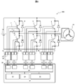
- FIG. 1 is a circuit diagram of an inverter device 100 according to Embodiment 1 of the present invention.
- the first embodiment is an inverter device to which a dual gate IGBT having a gate capable of two independent controls is applied as an IGBT.
- Dual gate IGBTs 1 to 6 which are semiconductor switching elements composed of an upper arm and a lower arm, are connected to a three-phase inductive load 10 (hereinafter also referred to as “motor 10”) that constitutes an AC motor.
- the Diodes 9 are connected to the dual gate IGBTs 1 to 6 in antiparallel.
- the dual gate IGBTs 1 to 6 are composed of two insulated gate terminals 7 and 8 (hereinafter simply referred to as “gate terminals”) and one emitter terminal 26, and a gate-emitter voltage applied to each of the two gate terminals. (Hereinafter referred to as “gate voltage”) to control conduction / non-conduction.
- gate voltage to control conduction / non-conduction.
- a conductive state is established by a gate voltage equal to or higher than a threshold voltage applied to at least one gate terminal
- a non-conductive state is established by a gate voltage less than the threshold voltage applied to two gate terminals.
- the inverter device 100 is supplied with DC power from the voltage source 11, and each of the IGBTs 1 to 6 repeats turn-on and turn-off at high speed by the gate voltage applied to the gate terminals 7 and 8 of the IGBTs 1 to 6, thereby inductive loads.
- AC power is supplied to 10. Thereby, a rotational force is given to the AC motor.
- the gate voltage of the dual gate IGBT 1 is generated by the gate drive circuits 12 to 17 connected to the IGBTs 1 to 6 of the three-phase upper and lower arms.
- the two gate terminals 7 and 8 of the dual gate IGBT and the two gate wirings output from the gate drive circuit 12 and connected to the two gate terminals 7 and 8 are electrically insulated from each other. It is independently controlled by the drive circuit 12.
- the emitter terminal 26 is also connected to the gate drive circuit 12 and is fixed to the internal reference potential.
- the gate drive circuit 12 includes a PWM signal conversion unit 20 that generates signals for driving the gates 7 and 8 of the dual gate IGBT 1 and two output buffers 18 and 19.
- the two output buffers 18 and 19 are supplied from a switching element (not shown) for adjusting the two PWM signals generated by the PWM signal conversion circuit 20 to a voltage that can turn on and off the gates 7 and 8 of the IGBT 1.
- Each of the PWM signal converters 20 has a function of receiving each PWM signal for the three-phase upper and lower arms and converting it into two PWM signals having a delay, and converts the input PWM signal into an insulated signal. It has a function.
- the PWM signal that is an input signal of the gate drive circuit 12 is generated by the PWM control calculation unit 22 provided in the PWM inverter control device 21 disposed on the substrate electrically separated from the gate drive circuit 12.
- the PWM control calculation unit 22 is a PWM whose conduction width is modulated based on the voltage command signal (modulation wave) of each of the three phases for driving the motor 10, the carrier wave (carrier wave), and the signal from the vector control calculation unit 25. It has a comparator and a calculator (not shown) for generating a signal.
- the vector control calculation unit 25 provided in the PWM inverter control device 21 reduces the knitting difference between the output current value of the IGBT detected by a current sensor (not shown) provided on the output line of the inverter and the set value.
- the control signal for realizing a high-quality inverter AC output signal is transmitted to the PWM control calculation unit 22.
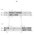
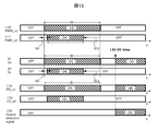
- FIG. 2 is a diagram illustrating control signals for realizing the inverter operation according to the first embodiment.
- FIG. 2 shows PWM signals 90 and 93 for commanding dual gate IGBTs arranged on the upper and lower arms of one phase among the three phases constituting the inverter, and two upper gate drive signals generated based on each. Gate signals 91 and 92 and lower arm gate signals 94 and 95 are shown.
- the PWM signal and the gate drive signal for commanding the dual gate IGBT arranged on the other two-phase upper and lower arms are signals that are shifted in phase by 120 ° from the signal shown in FIG. 2 (not shown). .
- the signal of the upper and lower arms generated by the PWM control calculation unit 22 has a timing to turn on / off in the opposite phase, and the upper and lower arms are simultaneously turned on to introduce the dual gate IGBT into a short circuit state.
- a non-lap period 102 in which the upper and lower arms are simultaneously turned off when switching on and off is provided.
- the non-wrapping period 102 is desirably 2 ⁇ sec to 20 ⁇ sec.
- one of the two gates of the dual gate IGBT is defined as a switching gate (Gs) and the other is defined as a carrier control gate (Gc).
- the Gs signal 91 is driven with the same conduction width and non-conduction width as the PWM signal 90.
- the dual gate IGBT becomes conductive or non-conductive and performs a switching operation.
- the Gc signal 92 shifts from OFF to ON with a certain delay time 99.
- the dual gate IGBT is turned on with a low transconductance, so that a rapid change dvce / dt of the collector-emitter voltage (Vce) is suppressed. Thereby, the effect of noise reduction at the time of turn-on can be achieved.
- the Gs signal 91 is turned off and the dual gate IGBT is turned off.
- the Gc signal 92 precedes the Gs signal 91.
- An off command is entered at.
- the carrier concentration inside the IGBT is reduced by the Gc signal 92 off command immediately before the turn-off switching, and the dual gate IGBT can be turned off at a higher speed and with a lower tail current. As a result, the effect of low power loss during turn-off can be achieved.
- the timing delay (delay) 99 between the Gs signal and the Gc signal at turn-on is preferably 1 ⁇ sec or more, and the timing delay (delay) 101 between the Gc signal and the Gs signal at turn-off is 5 ⁇ sec or more. Is desirable.
- Gs and Gc signals are input at the same timing and conduction width as described above according to the input PWM signal.
- the above-described two Gs signals 91 and Gc signals 92 and their delay times 99 and 101 are provided in the gate drive circuit 12 arranged for each of the three-phase upper and lower arms. It is derived by the PWM signal conversion circuit 20.
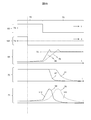
- FIG. 3A shows a voltage and current waveform 103 at the time of turn-off switching of the dual gate IGBT
- FIG. 3B shows a voltage and current waveform 104 at the time of the turn-on switching of the dual gate IGBT.
- the solid line indicates the characteristics of the dual gate IGBT
- the broken line indicates the characteristics of the conventional single gate IGBT.
- the voltage waveforms are 76 and 86
- the current waveforms are 77 and 87.
- the dual gate IGBT lowers the carrier concentration by applying a command to turn off Gc before Gs immediately before the turn-off switching.
- dvce / dt increases compared to the conventional case, and Vce increases to the power supply voltage 75 at a high speed (voltage waveform 86).
- the current transitions to 0 A at a high speed, and the tail period of the current is reduced (current waveform 87).
- the power loss caused by the product of the current and the voltage is smaller in the dual gate IGBT than in the conventional single gate IGBT (voltage waveform 76 and current waveform 77), and the effect of reducing the turn-off loss is achieved.
- the turn-on is performed by the gate signal on one side, that is, the Gs on signal. (Current waveform 87).
- the diode connected in reverse parallel to the dual-gate IGBT of the opposite arm is in a recovery state in which the flow state shifts to the reverse blocking state. Due to the low dic / dt characteristics of the dual gate IGBT, the current jump due to the recovery current of the arm diode is suppressed, the turn-on loss is reduced, and the noise due to the current is also suppressed and reduced.
- the dual gate IGBT it is possible to achieve an effect of reducing loss and reducing noise.
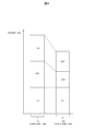
- FIG. 4 shows an inverter loss 105 (left bar graph) by the inverter device to which the conventional single gate IGBT is applied and an inverter loss 106 (right bar graph) by the inverter device to which the dual gate IGBT according to the present invention is applied.
- FIG. FIG. 4 shows the power loss generated by the IGBT element in the inverter device and its breakdown. The power loss that occurs during the inverter operation in the IGBT is occupied by the conduction loss 107, the turn-off switching loss 108, and the turn-on switching loss 109.
- the turn-off switching loss 108 and the turn-on switching loss 109 are switching losses that occur when the IGBT changes between conduction and non-conduction.
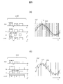
- FIG. 5A shows an input signal 110 and a one-phase output current waveform 114 of the inverter device by the dual gate IGBT according to the present invention
- FIG. 5B shows a dual gate to which the present invention is not applied. It is a figure which shows the input signal 111 of the inverter apparatus by IGBT, and the output current waveform 154 of 1 phase.
- the inverter device using the dual gate IGBT to which the present invention is not applied an example in which the conduction width of the Gs signal is long with respect to the PWM signal is shown.
- the conduction width of the Gs signal and the conduction width of the PWM signal are equal (FIG. 5A), and the current pulsation (ripple) in the output current 114 is compared to the inverter device to which the present invention is not applied. ) Can generate a small sine wave and the quality of the AC waveform is high. This is an effect obtained by controlling the conduction / non-conduction width of the dual gate IGBT equally with respect to the PWM signal on / off command.
- the conduction width of the Gs signal is long with respect to the PWM signal ON command, when the interval between the PWM ON command and the next PWM ON command is narrowed, By eliminating the interval between the Gs signals, the IGBT conduction time becomes longer than the command (FIG. 5B).
- the conduction time is substantially longer than the command, the pulsation of the output current 154 increases, the reproducibility of the modulated wave is low, and the quality of the AC waveform is inferior.
- FIG. 6 is a circuit diagram of an inverter device 200 according to Embodiment 2 of the present invention.
- the second embodiment is an inverter device to which a dual gate IGBT having two gates that can be independently controlled is applied to the IGBT.
- the same components as those in the first embodiment are given the same numbers.
- the difference from the first embodiment lies in the internal configuration of the gate drive circuits 12 to 17 and the PWM control calculation unit 22, and the other components are the same as those in the first embodiment, and thus the description thereof is omitted.
- the two PWM signals are also generated by the PWM control calculation unit 22 in the PWM inverter control device 21 arranged on the substrate electrically separated from the gate drive circuits 12 to 17 as in the first embodiment.
- the PWM control calculation unit 22 receives the signals from the carrier frequency calculation unit 23, the modulation wave calculation unit 24, and the vector control calculation unit 25 and generates the dual gate IGBTs 1 to 3 of the three-phase upper and lower arms based on the optimum command signal.
- Two PWM signals that determine the conduction / non-conduction timing of 6 are output and connected to the gate drive circuits 12-17.
- the PWM signal conversion unit 20 adopts a configuration built in the PWM control calculation unit 22 without being arranged on the substrate constituting the gate drive circuits 12 to 17, and is dual. Two PWM signals that command the driving of the gate IGBT are generated.
- Each gate drive circuit 12-17 receives two PWM signals for each phase and each arm. For example, taking the gate drive circuit 12 as an example, two PWM signals are converted into isolated signals, and voltage converted by output buffers 18 and 19, respectively.
- the PWM control calculation unit 22 is configured inside the PWM inverter control device 21 arranged on a substrate electrically separated from the gate drive circuit 12. In the configuration of the second embodiment, each of the gate drive circuits 12 to 17 does not require a PWM signal conversion unit, so that the volume of the inverter device can be reduced as compared with the first embodiment.
- FIG. 7 is a diagram showing control signals for realizing the inverter operation in the second embodiment.
- FIG. 7 shows two PWM_u1 116 and PWM_u2 117, and PWM_x1 118 and PWM_x2 119 as control signals for commanding the dual gate IGBTs arranged in the upper and lower arms of one phase among the three phases constituting the inverter. Show.
- the command signals and the gate drive signals of the dual gate IGBTs arranged on the other two-phase upper and lower arms are signals that are shifted in phase by 120 ° from the signals shown in FIG.
- the switching gate (Gs) receives the command signals u1, x1, v1, y1, w1, and z1, and the carrier control gate (Gc) has u2, x2, v2, It is assumed that it operates in response to command signals y2, w2 and z2.
- the conduction time of the dual gate IGBT is determined by the ON time of Gs, and the command signals of u1, x1, v1, y1, w1 and z1 in the PWM signal realize the AC output sine wave of the inverter. 23, a signal calculated by the modulation wave calculation unit 24 and the vector control calculation unit 25.
- the command signals for u2, x2, v2, y2, w2, and z2 are shorter than the on width in the commands for u1, x1, v1, y1, w1, and z1, and u1, x1, v1, y1, w1, and z1 are on.
- An ON command is input after the command is input, and an OFF command is input before the OFF commands for u1, x1, v1, y1, w1, and z1 are input.
- the upper and lower arm signals have the timing to turn on and off in reverse phase, and the upper and lower arms are simultaneously turned on to prevent the dual gate IGBT from being short-circuited.
- a non-lap period 102 in which the upper and lower arms are simultaneously turned off at the time of switching is provided between u1 and x1, between v1 and y1, and between w1 and z1.
- the non-wrapping period 102 is desirably 2 ⁇ s to 20 ⁇ s.
- the conduction / non-conduction of the dual gate IGBT is controlled by the timings u1, x1, v1, y1, w1, and z1, and is performed by the gate voltage of Gs connected to each through a gate drive circuit.
- Gs receives a PWM command of u1, x1, v1, y1, w1, and z1, and after changing from an off state to an on state, provides a certain delay time, and u2, x2, v2, y2 , W2 and z2 are received in response to the PWM command to change from OFF to ON.
- the dual gate IGBT is turned on with low transconductance, so that a steep collector-emitter voltage (Vce) change dvce / dt is suppressed.
- Vce collector-emitter voltage
- Gs precedes u2, x2, v2 immediately before Gs receives a PWM command of u1, x1, v1, y1, w1, and z1 and changes from on to off.
- Y2, w2 and z2 are received in response to the PWM command to change from on to off.
- the carrier concentration inside the IGBT is reduced by the Gc off signal immediately before the turn-off switching, and the dual gate IGBT can be turned off at a higher speed and with a lower tail current.
- the effect of the low power loss at the time of turn-off described above can be derived.
- the timing delay (delay) between the Gs signal and the Gc signal at turn-on is preferably 1 ⁇ sec or more
- the timing delay (delay) between the Gc signal and the Gs signal at turn-off is preferably 5 ⁇ sec or more.
- the PWM commands for u1, x1, v1, y1, w1, and z1, and u2, x2, v2, y2, w2, and z2 are set so that the above delay can be secured.
- the two PWM signals having the above delay time are generated in the PWM signal conversion unit 20 arranged in the PWM control calculation unit 22.
- the two PWM signals that determine the operation timing of the two gate signals of the dual gate IGBT are generated by a programmable integrated circuit (for example, a gate array) that constitutes the PWM control calculation unit 22, but depending on the command pulse width Different patterns of signals can be generated.
- FIG. 8 is a flowchart showing a sequence for determining two gate signals (Gs and Gc) of the dual gate IGBT in the second embodiment.
- step S1 the PWM control calculation unit 22 calculates the PWM command pulse width based on the carrier frequency and the modulation wave frequency. In step S2, it is determined whether or not the calculated command pulse width is larger than the timing delay.
- the Gc signal sets a one-side flow (Gc off) command to maintain non-conduction, and the process proceeds to the following step S4. Thereby, even in the narrow-width operation, conduction / non-conduction can be controlled in the dual gate IGBT.
- the determination is “yes”, that is, an ON command having a normal width longer than the timing delay is set for step S4.
- step S4 the PWM control calculation unit 22 calculates the pattern of the two gate signals (Gs and Gc) having a delay as described above based on the command in step S2 or S3. A command signal is output.
- FIG. 9 is a diagram showing command signals 116 to 119 for u1 and u2 during the normal width operation and the narrow width operation.
- FIG. 9A shows a normal width operation
- FIG. 9B shows a narrow width operation.
- two command signals u1 and u2 having a timing delay drive the dual gate IGBT.
- u2 maintains an off state, and a command having an on / off pattern is output only to u1.
- the two command signals can be changed optimally according to the ON command width calculated by the carrier frequency calculation unit 23, the modulation wave calculation unit 24, and the vector control calculation unit 25.
- FIG. 10 is a circuit diagram of an inverter device 300 according to the third embodiment of the present invention.
- the third embodiment is also an inverter device to which a dual gate IGBT having two gates that can be independently controlled is applied to the IGBT as in the first and second embodiments.
- the same components as those in the first embodiment are given the same numbers.
- the difference from the first embodiment is that an abnormal operation detection function is provided in the gate drive circuits 12 to 17 and the PWM control calculation unit 22, and the other components are the same as in the first embodiment. Is omitted.
- the following configuration is added to the circuit configuration of the first embodiment in order to detect an abnormal operation. Since the same configuration is added to each of the dual-gate IGBTs 1 to 6 of the three-phase upper and lower arms, the dual-gate IGBT 1 will be described as an example.
- the signal line of the switching gate (Gs) terminal 7 for controlling the conduction / non-conduction timing of the dual gate IGBT 1 is received by the level conversion unit 27 in the gate drive circuit 12 and sent to the PWM control calculation unit 22 in the PWM inverter control device 21.
- a feedback signal line 28 for returning is provided.
- the feedback signal line 28 senses the operation signal at the Gs terminal 7 by detecting the terminal voltage of the Gs terminal 7 of the dual gate IGBT 1, and uses the Gs on / off operation information as a feedback signal to the PWM control calculation unit 22.
- the PWM control calculation unit 22 composed of a programmable integrated circuit (for example, a gate array) compares the PWM command and the feedback signal, determines the difference of the feedback signal with respect to the PWM command, and alarms if they are different. And a function of shutting off the ON command and issuing an OFF command.
- FIG. 11 is a diagram illustrating the feedback (FB) signal and the abnormality detection signal in the third embodiment together with the gate control signal.
- the PWM control calculation unit 22 compares the PWM command with the feedback signal, and performs PWM control. The difference in the feedback signal with respect to the command can be determined. Therefore, when the dual gate IGBT performs an operation different from the PWM command in response to the PWM command, a warning signal or the like can be issued from the PWM control calculation unit 22.
- the PWM control calculation unit 22 that has received the feedback (FB) signal 128 can detect an abnormality by comparison with the PWM command 90. With this function, it is possible to prevent a situation in which the dual gate IGBT element can be destroyed due to a short circuit between the upper and lower arms due to an erroneous ON operation by resetting the PWM command based on the abnormality detection signal 129.
- the PWM control calculation unit 22 applies the Gs signal and Gc to the dual gate IGBT that detects the abnormality and the other dual gate IGBT that forms the upper and lower arms in pairs with the dual gate IGBT that detects the abnormality. Reset the PWM command for the signal to the non-conduction command.
- the feedback (FB) signal 128 in the third embodiment is an effective information source for detecting a failure in the inverter device.
- the signal line from the Gs terminal 7 and the feedback signal line 28 are provided for the circuit configuration of the first embodiment.
- a signal line may be provided.
- FIG. 12 is a circuit diagram of an inverter device 400 according to the fourth embodiment of the present invention.
- the fourth embodiment is also an inverter device to which a dual gate IGBT having two gates that can be independently controlled is applied to the IGBT as in the first to third embodiments.
- the circuit configuration of the fourth embodiment is based on the circuit configuration of the second embodiment, that is, unlike the first embodiment, the PWM signal conversion unit 20 is provided on the substrate constituting the gate drive circuits 12 to 17. Switching gate that does not exist and is built in the PWM control calculation unit 22 and controls the conduction / non-conduction timing of the dual gate IGBT in each of the dual gate IGBTs 1 to 6 of the three-phase upper and lower arms according to the third embodiment.
- a signal line for detecting the terminal voltage of the (Gs) terminal 7 is provided, and in addition, a signal line for detecting the terminal voltage of the carrier control gate (Gc) terminal 8 is also provided (here, the dual gate IGBT1). Taking the example as an example).
- level conversion units 27 and 29 are provided in the gate drive circuit 12 and feedback signal lines 28 and 30 are provided to return to the PWM control calculation unit 22 in the PWM inverter control device 21.
- the feedback signal lines 28 and 30 detect the terminal voltage of the Gs terminal 7 and the terminal voltage of the Gc terminal 8 of the dual gate IGBT 1 and notify the same ON / OFF operation information as the Gs signal and Gc signal as feedback signals.
- the PWM control calculation unit 22 composed of a programmable integrated circuit (for example, a gate array) judges the difference of the feedback signal with respect to the PWM command, and if it is different, shuts off the function that issues an alarm or the ON command Has a function of issuing an OFF command.
- FIGS. 13 and 14 are diagrams showing the feedback (FB) signal and the abnormality detection signal together with the gate control signal in the fourth embodiment. Since the feedback signal line 28 notifies the same information on the ON / OFF operation timing as the Gs signal as a feedback signal, the PWM control calculation unit 22 is configured to provide a feedback signal for the PWM command (conduction / non-conduction of the dual gate IGBT). The difference in operation) can be determined.
- the PWM control calculation unit 22 provides a feedback signal for the PWM command (operation based on the Gc signal). Can be judged. Therefore, when the Gs signal and Gc signal of the dual gate IGBT perform operations different from the PWM command in response to the PWM command, a warning signal can be issued from the PWM control calculation unit 22.
- the dual gate IGBT is erroneously turned on 130 via its own Gs terminal for some reason.
- the PWM control calculation unit 22 receives the feedback signal FB_u1 signal 131 via the feedback signal line 28, the abnormality can be detected by comparison with the PWM command (PWM_u1 signal 116).
- the dual gate IGBT is erroneously turned on via its own Gc terminal 130 for some reason.
- the PWM control calculation unit 22 that has received the feedback signal FB_u2 signal 132 via the feedback signal line 30 can detect an abnormality by comparison with the PWM command (PWM_u2 signal 117).
- each feedback signal in the fourth embodiment is an effective information source for detecting a failure in the inverter device.
- the signal lines from the Gs terminal 7 and the Gc terminal 8, the feedback signal line 28, and the feedback signal line 29 are provided in the circuit configuration of the second embodiment. These signal lines may be provided for one circuit configuration.
- FIG. 15 is a circuit diagram of an inverter device 500 according to the fifth embodiment of the present invention.
- an inverter device using a dual gate IGBT having two independent gates that can be controlled independently is connected to the dual gate IGBT in antiparallel.
- a Schottky barrier diode (SiC-SBD) using SiC (silicon carbide, silicon carbide) as a semiconductor substrate is employed.
- circuit configuration shown in FIG. 15 is the same as that of the first embodiment except for the difference in the Schottky barrier diode described above, and the description thereof is omitted. Further, the circuit configuration of the fifth embodiment is not limited to the circuit configuration of the first embodiment, and may be the circuit configurations of the second to fourth embodiments.
- the power loss in the inverter device caused by the inverter operation is constituted by the recovery loss and conduction loss of the diode connected in antiparallel in addition to the above-described IGBT conduction loss, turn-off loss and turn-on loss.
- the recovery loss is a power loss caused by a current-voltage product from the recovery current and the applied reverse voltage.
- This recovery current depends on the carrier in the conduction state of the diode, and in a pn diode in which the carrier is composed of both holes and electrons, it takes time until the carrier contributing to the conductivity modulation disappears.
- the Schottky barrier diode is composed of one of an electron and a hole, the carrier immediately disappears in the reverse blocking state, and the recovery current is reduced.
- SiC-SBD in which SiC is applied to a semiconductor substrate also has a high breakdown voltage performance.
- the fifth embodiment in which the SiC-SBD 31 and the dual gate IGBT 1 are combined as the inverter device 500 can reduce the recovery loss in addition to the turn-off loss and the turn-on loss, and can provide a further low-loss inverter device. become.
- an inverter device that can obtain an AC output with low power loss and low noise can be provided. It is possible to maintain a high-quality AC sine wave that can be operated even with a short pulse, and it is also possible to realize high reliability that can detect an abnormal operation and ensure safety.
- SiC Schottky barrier diode SiC-SBD
- 40 Diode, 41 ... U-phase upper arm IGBT ( Conventional single gate type), 42 ... U-phase lower arm IGBT (conventional single gate type), 43 ... V phase upper arm IGBT (conventional single gate type), 44 ... V phase lower arm IGBT (conventional single gate type) Single gate type), 45 ... W-phase upper arm IGBT (conventional single gate type), 46 ... W-phase lower arm IGBT Conventional single gate type), 47... Gate, 48... U phase upper arm gate drive circuit, 49. U phase lower arm gate drive circuit, 50. V phase upper arm gate drive circuit, 51. Gate drive circuit of 52 phase W upper arm, 53 ...
- Dual gate IGBT Current / voltage product 90 ... upper arm PWM signal, 91 ... upper arm Gs signal, 92 ... upper arm Gc signal, 93 ... lower arm WM signal, 94 ... lower arm Gs signal, 95 ... lower arm Gc signal, 96 ... PWM signal conduction command period, 97 ... Gs signal conduction command period, 98 ... Gc signal conduction command period, 99 ... turn-on delay period, DESCRIPTION OF SYMBOLS 100 ... Inverter apparatus which concerns on Example 1, 101 ... Turn-off delay period, 102 ... Non-wrap period, 103 ... Voltage and current waveform at the time of turn-off switching, 104 ...
Abstract
The purpose of the present invention is to provide a PWM-controlled inverter device that has less power loss than a PWM-controlled inverter device using a single gate IGBT and outputs an AC wave having small ripple and low noise. The inverter device is configured such that first and second dual gate IGBTs are used for the upper and lower arms of each of the three phases and diodes are connected in reverse parallel therewith. A first gate terminal of the first dual gate IGBT is driven by a first gate signal which is generated using a first PWM signal obtained by modulating a conduction width on the basis of a voltage command signal. A second gate terminal is driven by a second gate signal generated using a third PWM signal which is modulated to have a conduction width shorter than the conduction width of the first PWM signal on the basis of the first PWM signal, and which is positioned within the period of the conduction width of the first PWM signal. First and second gate signals for the second dual gate IGBT are similarly generated from a second PWM signal obtained by reversing the positive or negative phase of the first PWM signal.
Description
本発明は、インバータ装置に関し、特に、鉄道車両等に使用されるモータをPWM(Pulse Width Modulation:パルス幅変調)制御により駆動するインバータ装置に好適である。
The present invention relates to an inverter device, and is particularly suitable for an inverter device that drives a motor used in a railway vehicle or the like by PWM (Pulse Width Modulation) control.
近年の省エネ、地球環境保全の世界的な動向に連動して、交流モータを用いる様々な製品に対して、そのモータの駆動源に電力変換装置が適用されている。中でも、電気鉄道車両や風力発電システムなど、モータ容量の大きな分野へ拡大している。特に、電気鉄道用のモータ駆動システムは、高効率を達成するためにモータ本体の高効率化やそれを駆動する変換器の高効率化が進められている。
In conjunction with recent global trends in energy saving and global environmental conservation, power converters are applied to the motor drive source for various products that use AC motors. Above all, it is expanding to fields with large motor capacity such as electric railway vehicles and wind power generation systems. In particular, in motor drive systems for electric railways, in order to achieve high efficiency, the efficiency of the motor body and the efficiency of the converter that drives the motor body are being promoted.
一般に、交流モータを可変速駆動するためには、直流電力を任意の周波数と電圧に変換する電力変換装置としてインバータが用いられ、インバータを構成する半導体スイッチング素子をPWM制御することにより、交流モータへの印加電圧および周波数を制御している。
In general, in order to drive an AC motor at a variable speed, an inverter is used as a power conversion device that converts DC power into an arbitrary frequency and voltage, and a PWM control is performed on a semiconductor switching element that constitutes the inverter. The applied voltage and frequency are controlled.
従来の一般的なインバータ装置の回路構成としては、例えば、特許文献1にも示されるように(図1)、交流モータを構成する3相の誘導性負荷に対し、上アームと下アームから構成される半導体スイッチング素子であるIGBTが接続される。インバータとして動作する際、IGBTには、導通損失とスイッチング損失と呼ばれる電力損失が発生する。
As a circuit configuration of a conventional general inverter device, for example, as shown in Patent Document 1 (FIG. 1), it is configured from an upper arm and a lower arm with respect to a three-phase inductive load constituting an AC motor. An IGBT which is a semiconductor switching element to be connected is connected. When operating as an inverter, the IGBT generates power loss called conduction loss and switching loss.
図16は、IGBTの導通時72および非導通時73における、ゲート信号68、コレクタ・エミッタ間の電圧波形69、コレクタ電流波形70および双方による電流・電圧積71を示す図である。ゲートにオン信号が印加されることによるIGBTの導通時においては、導通により電流が流れると共に、オン電圧がコレクタ・エミッタ間に印加される。これは、IGBTの内部のキャリアに起因した抵抗による電圧降下であり、このオン電圧と電流の積78によって電力損失140が発生する。次に、ゲートにオフ信号が印加されると、IGBTの内部のキャリアが排出されてコレクタ・エミッタ間電圧が上昇し、その電圧がインバータの印加電圧75に達すると、キャリアの排出が止まり、電流が低下する。このオン状態からオフ状態に推移する際に電流・電圧積78は上昇し、ターンオフ損失と呼ぶ電力損失141が生じる。さらに、ゲートにオフ状態からオン信号が印加する際も、同様の原理で電流・電圧積が上昇し、ターンオン損失と呼ぶ電力損失が生じる。このターンオフ損失とターンオン損失との和がスイッチング損失である。
FIG. 16 is a diagram showing a gate signal 68, a collector-emitter voltage waveform 69, a collector current waveform 70, and a current / voltage product 71 of both when the IGBT is on 72 and when it is off 73. FIG. When the IGBT is turned on by applying an ON signal to the gate, a current flows due to the conduction and an ON voltage is applied between the collector and the emitter. This is a voltage drop due to resistance caused by the carriers inside the IGBT, and a power loss 140 is generated by the product 78 of the ON voltage and current. Next, when an off signal is applied to the gate, the carriers inside the IGBT are discharged and the collector-emitter voltage rises. When the voltage reaches the applied voltage 75 of the inverter, the carrier discharge stops and the current flows. Decreases. When transitioning from the on state to the off state, the current / voltage product 78 increases, and a power loss 141 called a turn-off loss occurs. Furthermore, when an ON signal is applied to the gate from the OFF state, the current / voltage product increases on the same principle, and a power loss called a turn-on loss occurs. The sum of this turn-off loss and turn-on loss is the switching loss.
インバータでは、このIGBTの導通損失とスイッチング損失とによって、素子が発熱する。そこで、これによる温度上昇を抑制するため、IGBT1つの素子に流す電流を制限し、並列数を増加することで温度規格を保ち所望の性能を得る対策を行っている。従って、1素子当たりに発生する電力損失を下げ、許容電流定格を増加することによって、体積当たりの変換効率の向上を図り、また素子の並列数が低減して素子の占有体積やコストの低減といった効果を生み出すことができる。
In the inverter, the element generates heat due to the conduction loss and switching loss of the IGBT. Therefore, in order to suppress the temperature rise due to this, measures are taken to maintain the temperature standard and to obtain the desired performance by limiting the current flowing through one IGBT element and increasing the parallel number. Therefore, by reducing the power loss generated per element and increasing the allowable current rating, the conversion efficiency per volume can be improved, and the number of parallel elements can be reduced to reduce the occupied volume and cost of the elements. Can produce effects.
また、IGBTの電力損失を低減できる技術として、特許文献2および3に示される2つのゲート端子から構成されるデュアルゲートIGBTがある。図17は、デュアルゲートIGBT79のシンボル図である。1つのコレクタ端子82、1つのエミッタ端子83に対し、2つのゲート端子80、81を有し、2つのゲート端子に入力するゲート信号によって、IGBTの導通・非導通を制御できるデュアルゲートIGBTである。図18は、デュアルゲートIGBT導通時のキャリア濃度プロファイルを示す図である。2つのゲートにオン信号を与えた場合85および1つのゲートにオン信号を与えてもう1つのゲートにオフ信号を与えた場合84のそれぞれのキャリア濃度を示している。2つのゲートにオン信号を与えた場合85は、エミッタからの正孔キャリアの注入が促進し、IGBT内部は高いキャリア濃度となり、これによってIGBT導通時のオン電圧を低減することができる。一方、1つのゲートにオン信号を与えて1つのゲートにオフ信号を与えた場合84は、正孔キャリアがエミッタへ排出され、これによって内部のキャリア濃度を低減することができる。つまり、デュアルゲートIGBTでは、新たに付加した1つのゲートとそれに与えるゲート電圧によって、IGBT導通時のキャリア濃度を変調することが可能である。この特徴を利用し、ターンオフスイッチングの直前に1つのゲート信号を先行してオフする駆動方式を適用することで、ターンオフ直前のキャリア濃度が下がり、低ターンオフ損失の特長を導出することができる。
Also, as a technology capable of reducing the power loss of the IGBT, there is a dual gate IGBT composed of two gate terminals shown in Patent Documents 2 and 3. FIG. 17 is a symbol diagram of the dual gate IGBT 79. This is a dual gate IGBT which has two gate terminals 80 and 81 for one collector terminal 82 and one emitter terminal 83 and can control the conduction / non-conduction of the IGBT by a gate signal inputted to the two gate terminals. . FIG. 18 is a diagram showing a carrier concentration profile when the dual gate IGBT is turned on. The carrier concentration is shown when the ON signal is given to two gates 85 and when the ON signal is given to one gate and the OFF signal is given to the other gate 84. When an ON signal is given to the two gates 85, injection of hole carriers from the emitter is promoted, and the inside of the IGBT has a high carrier concentration, whereby the ON voltage at the time of IGBT conduction can be reduced. On the other hand, when an ON signal is given to one gate and an OFF signal is given to one gate, hole carriers are discharged to the emitter, thereby reducing the internal carrier concentration. That is, in the dual gate IGBT, it is possible to modulate the carrier concentration at the time of IGBT conduction by the newly added one gate and the gate voltage applied thereto. By utilizing this feature and applying a driving method in which one gate signal is turned off immediately before the turn-off switching, the carrier concentration immediately before the turn-off is lowered, and the feature of low turn-off loss can be derived.
本願発明者が、デュアルゲートIGBTをモータ駆動用のPWM制御インバータ装置に適用することについて鋭意検討した結果、次の知見を得るに至った。
The inventor of the present application diligently studied about applying the dual gate IGBT to the PWM control inverter device for driving the motor, and as a result, the following knowledge was obtained.
本発明は、デュアルゲートIGBTの2つのゲート信号を適当なタイミングで導入することで、低損失な効果を導出するものである。図19は、デュアルゲートIGBTの導通時72および非導通時73における、2つのゲート信号68と143、コレクタ・エミッタ間の電圧波形69、コレクタ電流波形70および双方による電流・電圧積71を示す図である。なお、図19で示すコレクタ・エミッタ間の電圧波形69、コレクタ電流波形70および電流・電圧積71において、実線がデュアルゲートIGBTの特性を示し、破線が従来のシングルゲート型IGBTの特性を示している。デュアルゲートIGBTでは、スイッチングゲート68がオン状態72からオフ信号が入力する直前において、もう一方のキャリア制御ゲート143に先行してオフ信号を導入する駆動手法を適用する。キャリア制御ゲート143がオフすることで、IGBT内部のキャリア濃度が低減し、オン電圧が一時的に増加する。その後にスイッチングゲート68がオフすることで、IGBTは導通状態から非導通状態へ推移するが、キャリア濃度が低い状態から非導通状態へ推移することで、IGBT内部の空乏化が促進し、従来に対し高速にコレクタ・エミッタ間電圧69が上昇する(波形86)。さらに、キャリアも高速に排出されることから、電流70も短時間で0Aへ推移する(波形87)こととなる。これによって、電流・電圧積71の時間積分により導出されるターンオフ損失142は、従来のシングルゲート型IGBTにおけるターンオフ損失141に比べて大幅に低減されることとなる。この特性により、デュアルゲートIGBTとその駆動手法は、電力変換機能の低損失化、高効率化に有効な技術である。
The present invention derives a low-loss effect by introducing two gate signals of the dual gate IGBT at an appropriate timing. FIG. 19 is a diagram showing two gate signals 68 and 143, a collector-emitter voltage waveform 69, a collector current waveform 70, and a current / voltage product 71 by both when the dual gate IGBT is turned on and off 73. It is. In the collector-emitter voltage waveform 69, the collector current waveform 70, and the current / voltage product 71 shown in FIG. 19, the solid line indicates the characteristics of the dual gate IGBT, and the broken line indicates the characteristics of the conventional single gate IGBT. Yes. In the dual gate IGBT, a driving method is applied in which an off signal is introduced prior to the other carrier control gate 143 immediately before the switching gate 68 is input from the on state 72 to the off signal. When the carrier control gate 143 is turned off, the carrier concentration inside the IGBT is reduced, and the on-voltage is temporarily increased. After that, the switching gate 68 is turned off, so that the IGBT shifts from a conductive state to a non-conductive state, but by shifting from a low carrier concentration state to a non-conductive state, depletion inside the IGBT is promoted. On the other hand, the collector-emitter voltage 69 rises at a high speed (waveform 86). Further, since the carrier is discharged at a high speed, the current 70 also changes to 0 A in a short time (waveform 87). As a result, the turn-off loss 142 derived by time integration of the current / voltage product 71 is significantly reduced as compared with the turn-off loss 141 in the conventional single gate IGBT. Due to this characteristic, the dual gate IGBT and its driving method are effective techniques for reducing the loss and increasing the efficiency of the power conversion function.
一方で、デュアルゲートIGBTをモータ駆動用のPWM制御インバータ装置に適用するためには、交流出力波形の品質と動作信頼性を維持して低損失性能を導出することのできる上下アームの駆動方式や、2つの駆動信号を生み出す回路およびその回路配置の最適化が必要不可欠であった。
On the other hand, in order to apply the dual gate IGBT to the PWM control inverter device for driving the motor, the driving method of the upper and lower arms that can derive the low loss performance while maintaining the quality and operation reliability of the AC output waveform, It has been essential to optimize the circuit that generates the two drive signals and the circuit arrangement.
本発明は、従来型のIGBTを用いたPWM制御のインバータ装置に対し、インバータの相各相の上下アームを構成するIGBTにデュアルゲートIGBTを適用して電力損失の低いインバータ装置を提供することを目的とする。
The present invention provides a low power loss inverter device by applying a dual gate IGBT to an IGBT that constitutes the upper and lower arms of each phase of an inverter with respect to a PWM control inverter device using a conventional IGBT. Objective.
上記課題を解決するため、本発明に係るインバータ装置は、半導体スイッチング素子として、第1および第2のゲート端子を有し、少なくとも一つのゲート端子に閾値電圧以上の電圧を印加することで非導通状態から導通状態へ移行し、第1および第2のゲート端子に閾値電圧未満の電圧を印加することで導通状態から非導通状態へ移行する特性を有するデュアルゲートIGBTを用いて、3相各相の上アームに接続される第1のデュアルゲートIGBTおよび当該3相各相の下アームに接続される第2のデュアルゲートIGBTと、第1および第2のデュアルゲートIGBTそれぞれに逆並列に接続されるダイオードとから構成され、第1のデュアルゲートIGBTの第1のゲート端子は、負荷を駆動制御するための電圧指令信号に基づいて導通幅を変調した第1のPWM信号を用いて生成した第1のゲート信号により駆動され、第1のデュアルゲートIGBTの第2のゲート端子は、第1のPWM信号に基づいて当該第1のPWM信号の導通幅より短い導通幅に変調しかつ当該第1のPWM信号の導通幅の期間内に位置する第3のPWM信号を用いて生成した第2のゲート信号により駆動され、第2のデュアルゲートIGBTの第1のゲート端子は、第1のPWM信号の正負を逆相にした第2のPWM信号を用いて生成した第3のゲート信号により駆動され、第2のデュアルゲートIGBTの第2のゲート端子は、第2のPWM信号に基づいて当該第2のPWM信号の導通幅より短い導通幅に変調しかつ当該第2のPWM信号の導通幅の期間内に位置する第4のPWM信号を用いて生成した第4のゲート信号により駆動されることを特徴とする。
In order to solve the above-described problems, an inverter device according to the present invention has first and second gate terminals as semiconductor switching elements, and is non-conductive by applying a voltage equal to or higher than a threshold voltage to at least one gate terminal. Using a dual-gate IGBT having a characteristic of shifting from a conductive state to a non-conductive state by applying a voltage lower than the threshold voltage to the first and second gate terminals, The first dual-gate IGBT connected to the upper arm and the second dual-gate IGBT connected to the lower arm of each of the three-phase phases, and the first and second dual-gate IGBTs are connected in antiparallel. The first gate terminal of the first dual gate IGBT is based on a voltage command signal for driving and controlling the load. The second gate terminal of the first dual-gate IGBT is driven based on the first PWM signal, and is driven by the first gate signal generated using the first PWM signal whose conduction width is modulated. Driven by a second gate signal generated by using a third PWM signal that is modulated to a conduction width shorter than the conduction width of the first PWM signal and is located within the conduction width period of the first PWM signal. The first gate terminal of the dual gate IGBT is driven by the third gate signal generated using the second PWM signal in which the positive and negative of the first PWM signal are reversed in phase, and the second dual gate IGBT The second gate terminal modulates the second PWM signal to a conduction width shorter than the conduction width of the second PWM signal based on the second PWM signal and is located within the conduction width period of the second PWM signal. PWM signal Characterized in that it is driven by a fourth gate signal generated on the household.
本発明によれば、インバータ動作において、IGBTがスイッチングする際のターンオフスイッチング損失およびターンオンスイッチング損失を低減させる効果を奏することにより、低損失と高品質を両立したモータ駆動用インバータ装置を提供することができる。
According to the present invention, it is possible to provide an inverter device for driving a motor that achieves both low loss and high quality by producing an effect of reducing turn-off switching loss and turn-on switching loss when the IGBT is switched in inverter operation. it can.
以下、図面を参照して、本発明の実施形態として、実施例1~実施例5について説明する。
Hereinafter, examples 1 to 5 will be described as embodiments of the present invention with reference to the drawings.
図1は、本発明の実施例1に係るインバータ装置100の回路図である。
本実施例1は、IGBTとして2つの独立制御が可能であるゲートを有するデュアルゲートIGBTを適用したインバータ装置である。交流モータを構成する3相の誘導性負荷10(以下では、「モータ10」という場合もある)に対し、上アームと下アームから構成される半導体スイッチング素子であるデュアルゲートIGBT1~6が接続される。デュアルゲートIGBT1~6には、それぞれ逆並列にダイオード9が接続される。 FIG. 1 is a circuit diagram of aninverter device 100 according to Embodiment 1 of the present invention.
The first embodiment is an inverter device to which a dual gate IGBT having a gate capable of two independent controls is applied as an IGBT.Dual gate IGBTs 1 to 6, which are semiconductor switching elements composed of an upper arm and a lower arm, are connected to a three-phase inductive load 10 (hereinafter also referred to as “motor 10”) that constitutes an AC motor. The Diodes 9 are connected to the dual gate IGBTs 1 to 6 in antiparallel.
本実施例1は、IGBTとして2つの独立制御が可能であるゲートを有するデュアルゲートIGBTを適用したインバータ装置である。交流モータを構成する3相の誘導性負荷10(以下では、「モータ10」という場合もある)に対し、上アームと下アームから構成される半導体スイッチング素子であるデュアルゲートIGBT1~6が接続される。デュアルゲートIGBT1~6には、それぞれ逆並列にダイオード9が接続される。 FIG. 1 is a circuit diagram of an
The first embodiment is an inverter device to which a dual gate IGBT having a gate capable of two independent controls is applied as an IGBT.
デュアルゲートIGBT1~6は、2つの絶縁ゲート端子7および8(以下、単に「ゲート端子」と称す)と1つのエミッタ端子26から構成され、該2つのゲート端子それぞれに印加するゲート・エミッタ間電圧(以下、「ゲート電圧」と称す)によって導通・非導通を制御する。すなわち、少なくとも1つのゲート端子に印加された閾値電圧以上のゲート電圧によって、導通状態となり、2つのゲート端子に印加された閾値電圧未満のゲート電圧によって、非導通状態となる。
The dual gate IGBTs 1 to 6 are composed of two insulated gate terminals 7 and 8 (hereinafter simply referred to as “gate terminals”) and one emitter terminal 26, and a gate-emitter voltage applied to each of the two gate terminals. (Hereinafter referred to as “gate voltage”) to control conduction / non-conduction. In other words, a conductive state is established by a gate voltage equal to or higher than a threshold voltage applied to at least one gate terminal, and a non-conductive state is established by a gate voltage less than the threshold voltage applied to two gate terminals.
インバータ装置100には、電圧源11から直流電力が供給され、IGBT1~6のゲート端子7および8に印加されるゲート電圧によって、IGBT1~6それぞれが高速にターンオン、ターンオフを繰り返して、誘導性負荷10に交流電力を供給する。これにより、交流モータに回転力が与えられる。
The inverter device 100 is supplied with DC power from the voltage source 11, and each of the IGBTs 1 to 6 repeats turn-on and turn-off at high speed by the gate voltage applied to the gate terminals 7 and 8 of the IGBTs 1 to 6, thereby inductive loads. AC power is supplied to 10. Thereby, a rotational force is given to the AC motor.
デュアルゲートIGBT1のゲート電圧は、3相上下アームのIGBT1~6の各々に接続したゲート駆動回路12~17によって生成される。ここで、デュアルゲートIGBTの2つのゲート端子7および8と、ゲート駆動回路12から出力され2つのゲート端子7および8それぞれに接続される2つのゲート配線は、各々が電気的に絶縁され、ゲート駆動回路12によって独立に制御される。また、エミッタ端子26もゲート駆動回路12に接続され、内部の基準電位に固定される。
The gate voltage of the dual gate IGBT 1 is generated by the gate drive circuits 12 to 17 connected to the IGBTs 1 to 6 of the three-phase upper and lower arms. Here, the two gate terminals 7 and 8 of the dual gate IGBT and the two gate wirings output from the gate drive circuit 12 and connected to the two gate terminals 7 and 8 are electrically insulated from each other. It is independently controlled by the drive circuit 12. The emitter terminal 26 is also connected to the gate drive circuit 12 and is fixed to the internal reference potential.
ゲート駆動回路の構成については、ゲート駆動回路12を例に採ると、デュアルゲートIGBT1のゲート7および8を駆動する信号を生成するPWM信号変換部20と2つの出力バッファ18および19とから構成される。2つの出力バッファ18および19は、PWM信号変換回路20で生成された2つのPWM信号を、IGBT1のゲート7および8をオン・オフできる電圧に調整するためのスイッチング素子(図示せず)等から構成される。PWM信号変換部20それぞれは、3相上下アームに対する各PWM信号を受けて、ディレイを設けた2つのPWM信号に変換する機能を有し、かつ入力されたPWM信号を絶縁された信号に変換する機能を有する。
Regarding the configuration of the gate drive circuit, taking the gate drive circuit 12 as an example, the gate drive circuit 12 includes a PWM signal conversion unit 20 that generates signals for driving the gates 7 and 8 of the dual gate IGBT 1 and two output buffers 18 and 19. The The two output buffers 18 and 19 are supplied from a switching element (not shown) for adjusting the two PWM signals generated by the PWM signal conversion circuit 20 to a voltage that can turn on and off the gates 7 and 8 of the IGBT 1. Composed. Each of the PWM signal converters 20 has a function of receiving each PWM signal for the three-phase upper and lower arms and converting it into two PWM signals having a delay, and converts the input PWM signal into an insulated signal. It has a function.
ゲート駆動回路12の入力信号であるPWM信号は、ゲート駆動回路12と電気的に分離した基板上に配置されるPWMインバータ制御装置21が備えるPWM制御演算部22により生成される。PWM制御演算部22は、モータ10を駆動する3相各相の電圧指令信号(変調波)、搬送波(キャリア波)およびベクトル制御演算部25からの信号に基づいて、導通幅の変調されたPWM信号を生成する比較器や演算器(図示せず)を有する。また、PWMインバータ制御装置21が備えるベクトル制御演算部25は、インバータの出力線に設けた電流センサ(図示せず)により検出されるIGBTの出力電流値と設定値との編差を小さくするための演算を行い、高品質なインバータ交流出力信号を実現するための制御信号をPWM制御演算部22へ伝える。
The PWM signal that is an input signal of the gate drive circuit 12 is generated by the PWM control calculation unit 22 provided in the PWM inverter control device 21 disposed on the substrate electrically separated from the gate drive circuit 12. The PWM control calculation unit 22 is a PWM whose conduction width is modulated based on the voltage command signal (modulation wave) of each of the three phases for driving the motor 10, the carrier wave (carrier wave), and the signal from the vector control calculation unit 25. It has a comparator and a calculator (not shown) for generating a signal. Further, the vector control calculation unit 25 provided in the PWM inverter control device 21 reduces the knitting difference between the output current value of the IGBT detected by a current sensor (not shown) provided on the output line of the inverter and the set value. The control signal for realizing a high-quality inverter AC output signal is transmitted to the PWM control calculation unit 22.
図2は、本実施例1に係るインバータ動作を実現するための制御信号を示す図である。図2には、インバータを構成する3相の内、1相の上下アームに配置されたデュアルゲートIGBTを指令するPWM信号90および93、それぞれを基に生成されたゲート駆動信号として、2つの上ゲート信号91と92および下アームゲート信号94と95を示している。ここで、それ以外の2相の上下アームに配置されたデュアルゲートIGBTを指令するPWM信号およびゲート駆動信号は、図2に図示した信号から120°位相をずらした信号である(図示せず)。
FIG. 2 is a diagram illustrating control signals for realizing the inverter operation according to the first embodiment. FIG. 2 shows PWM signals 90 and 93 for commanding dual gate IGBTs arranged on the upper and lower arms of one phase among the three phases constituting the inverter, and two upper gate drive signals generated based on each. Gate signals 91 and 92 and lower arm gate signals 94 and 95 are shown. Here, the PWM signal and the gate drive signal for commanding the dual gate IGBT arranged on the other two-phase upper and lower arms are signals that are shifted in phase by 120 ° from the signal shown in FIG. 2 (not shown). .
PWM制御演算部22より生成された上下アームの信号は、逆相にてオン・オフするタイミングを有し、また上下アームが同時にオンの信号を導入し、デュアルゲートIGBTが短絡状態となることを防ぐために、オン・オフの切替時に、上下アームが同時にオフする非ラップ期間102を設けている。非ラップ期間102としては、2μ秒~20μ秒が望ましい。
The signal of the upper and lower arms generated by the PWM control calculation unit 22 has a timing to turn on / off in the opposite phase, and the upper and lower arms are simultaneously turned on to introduce the dual gate IGBT into a short circuit state. In order to prevent this, a non-lap period 102 in which the upper and lower arms are simultaneously turned off when switching on and off is provided. The non-wrapping period 102 is desirably 2 μsec to 20 μsec.
ここで、デュアルゲートIGBTの2つのゲートの一方をスイッチングゲート(Gs)、他方をキャリア制御ゲート(Gc)と定義する。Gs信号91は、PWM信号90と同じ導通幅および非導通幅で駆動する。このGs信号91のタイミングにより、デュアルゲートIGBTは導通または非導通状態となり、スイッチング動作を行う。一方、Gc信号92は、Gs信号91がオフからオン状態に変化した後、一定のディレイ時間99を設けてオフからオン状態に移行する。この制御により、デュアルゲートIGBTは低いトランスコンダクタンスによってターンオンするため、コレクタ・エミッタ間電圧(Vce)の急峻な変化dvce/dtが抑制される。これによって、ターンオン時のノイズ低減の効果を奏することができる。
Here, one of the two gates of the dual gate IGBT is defined as a switching gate (Gs) and the other is defined as a carrier control gate (Gc). The Gs signal 91 is driven with the same conduction width and non-conduction width as the PWM signal 90. Depending on the timing of the Gs signal 91, the dual gate IGBT becomes conductive or non-conductive and performs a switching operation. On the other hand, after the Gs signal 91 changes from OFF to ON, the Gc signal 92 shifts from OFF to ON with a certain delay time 99. By this control, the dual gate IGBT is turned on with a low transconductance, so that a rapid change dvce / dt of the collector-emitter voltage (Vce) is suppressed. Thereby, the effect of noise reduction at the time of turn-on can be achieved.
一方、Gs信号91がPWM信号90と同じ導通幅の後、オンからオフ信号が入ってデュアルゲートIGBTがターンオフすることになるが、このタイミングの直前において、Gs信号91に先行してGc信号92にオフ指令が入る。この制御により、デュアルゲートIGBTは、ターンオフスイッチング直前に、Gc信号92のオフ指令によってIGBT内部のキャリア濃度が低減し、より高速でかつ低いテール電流でのターンオフスイッチングが可能となる。これによって、ターンオフ時の低電力損失の効果を奏することができる。さらに、デュアルゲートIGBTが導通時は、Gs信号91とGc信号92の両者のゲートにオン指令が入るため、IGBT内部のキャリア濃度を高め、低い導通損失の効果も奏することができる。ここで、ターンオン時のGs信号とGc信号とのタイミング遅延(ディレイ)99は、1μ秒以上が望ましく、また、ターンオフ時のGc信号とGs信号とのタイミング遅延(ディレイ)101は、5μ秒以上が望ましい。
On the other hand, after the same conduction width as that of the PWM signal 90, the Gs signal 91 is turned off and the dual gate IGBT is turned off. Just before this timing, the Gc signal 92 precedes the Gs signal 91. An off command is entered at. By this control, the carrier concentration inside the IGBT is reduced by the Gc signal 92 off command immediately before the turn-off switching, and the dual gate IGBT can be turned off at a higher speed and with a lower tail current. As a result, the effect of low power loss during turn-off can be achieved. Further, when the dual gate IGBT is conducting, an ON command is input to the gates of both the Gs signal 91 and the Gc signal 92, so that the carrier concentration inside the IGBT can be increased and the effect of low conduction loss can be achieved. Here, the timing delay (delay) 99 between the Gs signal and the Gc signal at turn-on is preferably 1 μsec or more, and the timing delay (delay) 101 between the Gc signal and the Gs signal at turn-off is 5 μsec or more. Is desirable.
対アームのデュアルゲートIGBT、また別相のデュアルゲートIGBTについても、入力のPWM信号に応じて、上記と同じタイミングと導通幅でGsとGcの信号が入るものとする。ここで、PWM信号90を受けて、上述した2つのGs信号91およびGc信号92、それらの遅延時間99および101は、3相上下アーム毎に配置されたゲート駆動回路12の内部に設けられたPWM信号変換回路20により導出される。
For the dual-arm IGBT of the pair arm and the dual-gate IGBT of another phase, it is assumed that Gs and Gc signals are input at the same timing and conduction width as described above according to the input PWM signal. Here, in response to the PWM signal 90, the above-described two Gs signals 91 and Gc signals 92 and their delay times 99 and 101 are provided in the gate drive circuit 12 arranged for each of the three-phase upper and lower arms. It is derived by the PWM signal conversion circuit 20.
次に、図3から5を参照して、本実施例1による効果を説明する。図3(a)に、デュアルゲートIGBTのターンオフスイッチング時の電圧および電流の波形103を、図3(b)に、デュアルゲートIGBTのターンオンスイッチング時の電圧および電流の波形104を示す。ここで、実線はデュアルゲートIGBT、破線は従来のシングルゲート型IGBT、の各特性を示し、電圧波形が76と86で、電流波形が77と87である。
Next, the effects of the first embodiment will be described with reference to FIGS. FIG. 3A shows a voltage and current waveform 103 at the time of turn-off switching of the dual gate IGBT, and FIG. 3B shows a voltage and current waveform 104 at the time of the turn-on switching of the dual gate IGBT. Here, the solid line indicates the characteristics of the dual gate IGBT, and the broken line indicates the characteristics of the conventional single gate IGBT. The voltage waveforms are 76 and 86, and the current waveforms are 77 and 87.
ターンオフスイッチング時において(図3(a))、デュアルゲートIGBTは、ターンオフスイッチング直前に、GcをGsに先行してオフする指令が適用されることにより、キャリア濃度を低下させる。これにより、従来に対し、dvce/dtが上昇し、高速に電源電圧75へVceが上昇する(電圧波形86)。さらにその後、高速に電流が0Aへ推移し、電流のテール期間が低減する(電流波形87)。この特性によって、電流と電圧の積により発生する電力損失が、デュアルゲートIGBTでは、従来のシングルゲート型IGBT(電圧波形76および電流波形77)に対し小さくなり、ターンオフ損失を低減させる効果を奏する。
At the time of turn-off switching (FIG. 3A), the dual gate IGBT lowers the carrier concentration by applying a command to turn off Gc before Gs immediately before the turn-off switching. As a result, dvce / dt increases compared to the conventional case, and Vce increases to the power supply voltage 75 at a high speed (voltage waveform 86). Thereafter, the current transitions to 0 A at a high speed, and the tail period of the current is reduced (current waveform 87). With this characteristic, the power loss caused by the product of the current and the voltage is smaller in the dual gate IGBT than in the conventional single gate IGBT (voltage waveform 76 and current waveform 77), and the effect of reducing the turn-off loss is achieved.
一方、ターンオンスイッチング時において(図3(b))、片側のゲート即ちGsのオン信号によってターンオンするため、その瞬間のIGBTのトランスコンダクタンスが下がり、コレクタ電流(Ic)の上昇dic/dtが低下する(電流波形87)。この際、対アームのデュアルゲートIGBTに逆並列接続されたダイオードが、通流状態から逆阻止状態へ推移するリカバリー状態となる。デュアルゲートIGBTの低dic/dtの特性によって、対アームダイオードのリカバリー電流起因の電流跳ね上がりが抑制され、ターンオン損失が下がると共に、その電流起因のノイズも抑制され低減する。
以上のように、デュアルゲートIGBTを適用することによって、損失低減と低ノイズ化の効果を奏することができる。 On the other hand, at the time of turn-on switching (FIG. 3B), the turn-on is performed by the gate signal on one side, that is, the Gs on signal. (Current waveform 87). At this time, the diode connected in reverse parallel to the dual-gate IGBT of the opposite arm is in a recovery state in which the flow state shifts to the reverse blocking state. Due to the low dic / dt characteristics of the dual gate IGBT, the current jump due to the recovery current of the arm diode is suppressed, the turn-on loss is reduced, and the noise due to the current is also suppressed and reduced.
As described above, by applying the dual gate IGBT, it is possible to achieve an effect of reducing loss and reducing noise.
図4は、従来のシングルゲート型IGBTを適用したインバータ装置によるインバータ損失105(左側の棒グラフ)と、本発明に係るデュアルゲートIGBTを適用したインバータ装置によるインバータ損失106(右側の棒グラフ)とを示す図である。図4では、インバータ装置の内のIGBT素子で発生する電力損失とその内訳を示している。IGBTでインバータ動作時に発生する電力損失は、導通損失107、ターンオフスイッチング損失108およびターンオンスイッチング損失109で占められる。この内、ターンオフスイッチング損失108およびターンオンスイッチング損失109が、IGBTが導通と非導通の間を推移する際に発生するスイッチング損失である。
FIG. 4 shows an inverter loss 105 (left bar graph) by the inverter device to which the conventional single gate IGBT is applied and an inverter loss 106 (right bar graph) by the inverter device to which the dual gate IGBT according to the present invention is applied. FIG. FIG. 4 shows the power loss generated by the IGBT element in the inverter device and its breakdown. The power loss that occurs during the inverter operation in the IGBT is occupied by the conduction loss 107, the turn-off switching loss 108, and the turn-on switching loss 109. Among these, the turn-off switching loss 108 and the turn-on switching loss 109 are switching losses that occur when the IGBT changes between conduction and non-conduction.
図示のとおり、デュアルゲートIGBTを採用することによって、IGBT特有の低い導通損失107を維持し、ターンオフスイッチング損失108およびターンオンスイッチング損失109をそれぞれ低減することができる。その効果はそれぞれ、およそ30%および10%の低減率である。これにより、インバータ装置にあってIGBTで発生する電力損失を、数10%低減できる効果を奏する。
As shown in the figure, by adopting the dual gate IGBT, it is possible to maintain the low conduction loss 107 specific to the IGBT and reduce the turn-off switching loss 108 and the turn-on switching loss 109, respectively. The effect is a reduction of approximately 30% and 10%, respectively. Thereby, there exists an effect which can reduce the electric power loss which generate | occur | produces in IGBT in an inverter apparatus by several 10%.
図5は、図5(a)に、本発明に係るデュアルゲートIGBTによるインバータ装置の入力信号110および1相の出力電流波形114を示し、図5(b)に、本発明を適用しないデュアルゲートIGBTによるインバータ装置の入力信号111および1相の出力電流波形154を示す図である。ここで、本発明を適用しないデュアルゲートIGBTによるインバータ装置では、PWM信号に対してGs信号の導通幅が長い場合の1例を示す。
FIG. 5A shows an input signal 110 and a one-phase output current waveform 114 of the inverter device by the dual gate IGBT according to the present invention, and FIG. 5B shows a dual gate to which the present invention is not applied. It is a figure which shows the input signal 111 of the inverter apparatus by IGBT, and the output current waveform 154 of 1 phase. Here, in the inverter device using the dual gate IGBT to which the present invention is not applied, an example in which the conduction width of the Gs signal is long with respect to the PWM signal is shown.
本発明に係るインバータ装置では、Gs信号の導通幅とPWM信号の導通幅とが等しく(図5(a))、本発明を適用しないインバータ装置と比較して、出力電流114において電流脈動(リップル)の小さい正弦波を生成でき、交流波形の品質が高い。これは、PWM信号のオン・オフ指令に対して、デュアルゲートIGBTの導通・非導通の幅をそれぞれ等しく制御することによる効果である。
In the inverter device according to the present invention, the conduction width of the Gs signal and the conduction width of the PWM signal are equal (FIG. 5A), and the current pulsation (ripple) in the output current 114 is compared to the inverter device to which the present invention is not applied. ) Can generate a small sine wave and the quality of the AC waveform is high. This is an effect obtained by controlling the conduction / non-conduction width of the dual gate IGBT equally with respect to the PWM signal on / off command.
一方、本発明を適用しないインバータ装置では、PWM信号のオン指令に対し、Gs信号の導通幅が長いため、PWMオン指令と次のPWMオン指令の間隔が狭くなる際に、Gs信号と次のGs信号の間隔が無くなることで、IGBTの導通時間が指令に対し長くなる(図5(b))。この制御では、導通時間が指令に対し実質長くなることから出力電流154の脈動は大きくなり、変調波の再現性が低く、交流波形の品質が劣ることとなる。
On the other hand, in the inverter device to which the present invention is not applied, since the conduction width of the Gs signal is long with respect to the PWM signal ON command, when the interval between the PWM ON command and the next PWM ON command is narrowed, By eliminating the interval between the Gs signals, the IGBT conduction time becomes longer than the command (FIG. 5B). In this control, since the conduction time is substantially longer than the command, the pulsation of the output current 154 increases, the reproducibility of the modulated wave is low, and the quality of the AC waveform is inferior.
したがって、本発明では、PWM指令におけるオン指令幅とGs信号の幅とを等しく設定することによって、交流出力波形の高い品質を実現する効果を奏することができる。
Therefore, in the present invention, by setting the ON command width and the width of the Gs signal in the PWM command to be equal, an effect of realizing high quality of the AC output waveform can be achieved.
図6は、本発明の実施例2に係るインバータ装置200の回路図である。
本実施例2も、先の実施例1と同様に、IGBTに2つの独立制御が可能であるゲートを有するデュアルゲートIGBTを適用したインバータ装置である。回路構成において、実施例1と同様の構成要素には、同じ付番をしている。実施例1との相違点は、ゲート駆動回路12~17およびPWM制御演算部22における内部構成にあり、その他の構成要素については実施例1と同様であるので、説明は省略する。 FIG. 6 is a circuit diagram of aninverter device 200 according to Embodiment 2 of the present invention.
As in the first embodiment, the second embodiment is an inverter device to which a dual gate IGBT having two gates that can be independently controlled is applied to the IGBT. In the circuit configuration, the same components as those in the first embodiment are given the same numbers. The difference from the first embodiment lies in the internal configuration of thegate drive circuits 12 to 17 and the PWM control calculation unit 22, and the other components are the same as those in the first embodiment, and thus the description thereof is omitted.
本実施例2も、先の実施例1と同様に、IGBTに2つの独立制御が可能であるゲートを有するデュアルゲートIGBTを適用したインバータ装置である。回路構成において、実施例1と同様の構成要素には、同じ付番をしている。実施例1との相違点は、ゲート駆動回路12~17およびPWM制御演算部22における内部構成にあり、その他の構成要素については実施例1と同様であるので、説明は省略する。 FIG. 6 is a circuit diagram of an
As in the first embodiment, the second embodiment is an inverter device to which a dual gate IGBT having two gates that can be independently controlled is applied to the IGBT. In the circuit configuration, the same components as those in the first embodiment are given the same numbers. The difference from the first embodiment lies in the internal configuration of the
次に、2つのPWM信号も、実施例1と同様に、ゲート駆動回路12~17と電気的に分離した基板上に配置されるPWMインバータ制御装置21内部のPWM制御演算部22により生成される。PWM制御演算部22は、キャリア周波数演算部23、変調波演算部24およびベクトル制御演算部25の信号を受けて生成される最適な指令信号に基づいて、3相上下アームの各デュアルゲートIGBT1~6の導通・非導通タイミングを決める2つのPWM信号を出力し、各ゲート駆動回路12~17と接続する。本実施例2に係るPWM信号変換部20は、実施例1とは異なり、ゲート駆動回路12~17を構成する基板に配置せずに、PWM制御演算部22に内蔵された構成を採り、デュアルゲートIGBTの駆動を指令する2つのPWM信号が生成される。
Next, the two PWM signals are also generated by the PWM control calculation unit 22 in the PWM inverter control device 21 arranged on the substrate electrically separated from the gate drive circuits 12 to 17 as in the first embodiment. . The PWM control calculation unit 22 receives the signals from the carrier frequency calculation unit 23, the modulation wave calculation unit 24, and the vector control calculation unit 25 and generates the dual gate IGBTs 1 to 3 of the three-phase upper and lower arms based on the optimum command signal. Two PWM signals that determine the conduction / non-conduction timing of 6 are output and connected to the gate drive circuits 12-17. Unlike the first embodiment, the PWM signal conversion unit 20 according to the second embodiment adopts a configuration built in the PWM control calculation unit 22 without being arranged on the substrate constituting the gate drive circuits 12 to 17, and is dual. Two PWM signals that command the driving of the gate IGBT are generated.
各ゲート駆動回路12~17は、各相、各アームそれぞれ2つのPWM信号の入力を受ける。例えば、ゲート駆動回路12を例に採ると、2つのPWM信号は絶縁された信号に変換され、出力バッファ18および19によってそれぞれ電圧変換される。PWM制御演算部22は、ゲート駆動回路12と電気的に分離した基板上に配置されるPWMインバータ制御装置21内部で構成される。本実施例2の構成では、各ゲート駆動回路12~17にはPWM信号変換部が不要であり、実施例1と比較してインバータ装置の省体積化を計ることが可能である。
Each gate drive circuit 12-17 receives two PWM signals for each phase and each arm. For example, taking the gate drive circuit 12 as an example, two PWM signals are converted into isolated signals, and voltage converted by output buffers 18 and 19, respectively. The PWM control calculation unit 22 is configured inside the PWM inverter control device 21 arranged on a substrate electrically separated from the gate drive circuit 12. In the configuration of the second embodiment, each of the gate drive circuits 12 to 17 does not require a PWM signal conversion unit, so that the volume of the inverter device can be reduced as compared with the first embodiment.
図7は、本実施例2におけるインバータ動作を実現するための制御信号を示す図である。図7には、インバータを構成する3相の内、1相の上下アームに配置されたデュアルゲートIGBTを指令する制御信号として、それぞれ2つのPWM_u1 116とPWM_u2 117、および、PWM_x1 118とPWM_x2 119を示している。ここで、それ以外の2相の上下アームに配置されたデュアルゲートIGBTの指令信号およびゲートの駆動信号は、図7に図示した信号から120°位相をずらした信号である。
FIG. 7 is a diagram showing control signals for realizing the inverter operation in the second embodiment. FIG. 7 shows two PWM_u1 116 and PWM_u2 117, and PWM_x1 118 and PWM_x2 119 as control signals for commanding the dual gate IGBTs arranged in the upper and lower arms of one phase among the three phases constituting the inverter. Show. Here, the command signals and the gate drive signals of the dual gate IGBTs arranged on the other two-phase upper and lower arms are signals that are shifted in phase by 120 ° from the signals shown in FIG.
また、デュアルゲートIGBTの2つのゲートの内、スイッチングゲート(Gs)は、u1、x1、v1、y1、w1およびz1の指令信号を受け、キャリア制御ゲート(Gc)は、u2、x2、v2、y2、w2およびz2の指令信号を受けて動作するものとする。デュアルゲートIGBTの導通時間はGsのオン時間で決まり、PWM信号の内、u1、x1、v1、y1、w1およびz1の指令信号は、インバータの交流出力正弦波を実現するため、キャリア周波数演算部23、変調波演算部24およびベクトル制御演算部25により算出された信号である。
Of the two gates of the dual gate IGBT, the switching gate (Gs) receives the command signals u1, x1, v1, y1, w1, and z1, and the carrier control gate (Gc) has u2, x2, v2, It is assumed that it operates in response to command signals y2, w2 and z2. The conduction time of the dual gate IGBT is determined by the ON time of Gs, and the command signals of u1, x1, v1, y1, w1 and z1 in the PWM signal realize the AC output sine wave of the inverter. 23, a signal calculated by the modulation wave calculation unit 24 and the vector control calculation unit 25.
一方、u2、x2、v2、y2、w2およびz2の指令信号は、u1、x1、v1、y1、w1およびz1の指令におけるオン幅より短く、u1、x1、v1、y1、w1およびz1のオン指令が入った後にオン指令が入り、u1、x1、v1、y1、w1およびz1のオフ指令が入る前にオフ指令が入る。
On the other hand, the command signals for u2, x2, v2, y2, w2, and z2 are shorter than the on width in the commands for u1, x1, v1, y1, w1, and z1, and u1, x1, v1, y1, w1, and z1 are on. An ON command is input after the command is input, and an OFF command is input before the OFF commands for u1, x1, v1, y1, w1, and z1 are input.
上下アームの信号は、逆相にてオン・オフするタイミングを有しており、また上下アームが同時にオンの信号を導入し、デュアルゲートIGBTが短絡状態となることを防ぐために、オン・オフの切替時に、上下アームが同時にオフする非ラップ期間102が、u1とx1との間、v1とy1との間およびw1とz1との間に設けている。ここで、非ラップ期間102は、2μ秒~20μ秒が望ましい。
The upper and lower arm signals have the timing to turn on and off in reverse phase, and the upper and lower arms are simultaneously turned on to prevent the dual gate IGBT from being short-circuited. A non-lap period 102 in which the upper and lower arms are simultaneously turned off at the time of switching is provided between u1 and x1, between v1 and y1, and between w1 and z1. Here, the non-wrapping period 102 is desirably 2 μs to 20 μs.
デュアルゲートIGBTの導通、非導通の制御は、u1、x1、v1、y1、w1およびz1のタイミングにより行われ、それぞれにゲート駆動回路を介して接続されたGsのゲート電圧により行われる。デュアルゲートIGBTのターンオン動作は、Gsがu1、x1、v1、y1、w1およびz1のPWM指令を受けて、オフからオン状態に変化した後一定のディレイ時間を設け、u2、x2、v2、y2、w2およびz2のPWM指令を受けて、オフからオン状態に変化するシーケンスにより行われる。この制御により、デュアルゲートIGBTは低いトランスコンダクタンスによってターンオンするため、急峻なコレクタ・エミッタ間電圧(Vce)の変化dvce/dtが抑制される。これによって、実施例1と同様に、前述したターンオン時のノイズ低減の効果を奏することができる。
The conduction / non-conduction of the dual gate IGBT is controlled by the timings u1, x1, v1, y1, w1, and z1, and is performed by the gate voltage of Gs connected to each through a gate drive circuit. In the turn-on operation of the dual gate IGBT, Gs receives a PWM command of u1, x1, v1, y1, w1, and z1, and after changing from an off state to an on state, provides a certain delay time, and u2, x2, v2, y2 , W2 and z2 are received in response to the PWM command to change from OFF to ON. By this control, the dual gate IGBT is turned on with low transconductance, so that a steep collector-emitter voltage (Vce) change dvce / dt is suppressed. As a result, like the first embodiment, the above-described noise reduction effect at turn-on can be achieved.
一方、デュアルゲートIGBTのターンオフ動作は、Gsがu1、x1、v1、y1、w1およびz1のPWM指令を受けて、オンからオフ状態に変化する直前に、Gcが先行してu2、x2、v2、y2、w2およびz2のPWM指令を受けて、オンからオフ状態に変化するシーケンスにより行われる。この制御により、デュアルゲートIGBTは、ターンオフスイッチング直前に、Gcのオフ信号によってIGBT内部のキャリア濃度が低減し、より高速でかつ低いテール電流でのターンオフスイッチングが可能となる。これによって、実施例1と同様に、前述したターンオフ時の低電力損失の効果を導出できる。
On the other hand, in the turn-off operation of the dual gate IGBT, Gs precedes u2, x2, v2 immediately before Gs receives a PWM command of u1, x1, v1, y1, w1, and z1 and changes from on to off. , Y2, w2 and z2 are received in response to the PWM command to change from on to off. By this control, the carrier concentration inside the IGBT is reduced by the Gc off signal immediately before the turn-off switching, and the dual gate IGBT can be turned off at a higher speed and with a lower tail current. As a result, similarly to the first embodiment, the effect of the low power loss at the time of turn-off described above can be derived.
さらに、デュアルゲートIGBTが導通時は、GsとGc両者のゲートにオン信号が入るため、IGBT内部のキャリア濃度を高められ、低い導通損失の効果を導出できる。ここで、ターンオン時のGs信号とGc信号のタイミング遅延(ディレイ)は、1μ秒以上が望ましく、また、ターンオフ時のGc信号とGs信号のタイミング遅延(ディレイ)は、5μ秒以上が望ましい。以上のディレイを確保できるように、u1、x1、v1、y1、w1およびz1、また、u2、x2、v2、y2、w2およびz2のPWM指令が設定される。なお、以上のディレイ時間を有した2つのPWM信号は、PWM制御演算部22に配置されたPWM信号変換部20において生成される。
Furthermore, when the dual gate IGBT is conducting, an ON signal is input to both the gates of Gs and Gc, so that the carrier concentration inside the IGBT can be increased and the effect of low conduction loss can be derived. Here, the timing delay (delay) between the Gs signal and the Gc signal at turn-on is preferably 1 μsec or more, and the timing delay (delay) between the Gc signal and the Gs signal at turn-off is preferably 5 μsec or more. The PWM commands for u1, x1, v1, y1, w1, and z1, and u2, x2, v2, y2, w2, and z2 are set so that the above delay can be secured. The two PWM signals having the above delay time are generated in the PWM signal conversion unit 20 arranged in the PWM control calculation unit 22.
次に、図8および9を参照して、先の実施例1で説明した効果に加え、本実施例2が奏する効果を説明する。
デュアルゲートIGBTの2つのゲート信号の動作タイミングを決める2つのPWM信号は、PWM制御演算部22を構成するプログラム可能な集積回路(例えば、ゲートアレイ)によって生成されるが、指令パルス幅に応じて異なるパターンの信号を生成できる。図8は、本実施例2におけるデュアルゲートIGBTの2つのゲート信号(GsおよびGc)を決定するシーケンスを示すフローチャートである。PWM制御においては、導通幅の変調された様々なオン指令幅をもった入力信号でIGBTを動作させる必要があるが、2つのゲート信号に設定するタイミングディレイよりも短いオン指令幅(狭幅指令)においても、本実施例2により正常に動作させることができる。 Next, with reference to FIGS. 8 and 9, in addition to the effects described in the first embodiment, the effects provided by the second embodiment will be described.
The two PWM signals that determine the operation timing of the two gate signals of the dual gate IGBT are generated by a programmable integrated circuit (for example, a gate array) that constitutes the PWMcontrol calculation unit 22, but depending on the command pulse width Different patterns of signals can be generated. FIG. 8 is a flowchart showing a sequence for determining two gate signals (Gs and Gc) of the dual gate IGBT in the second embodiment. In the PWM control, it is necessary to operate the IGBT with an input signal having various on command widths whose conduction widths are modulated, but the on command width (narrow command) which is shorter than the timing delay set for the two gate signals. ) Can be normally operated according to the second embodiment.
デュアルゲートIGBTの2つのゲート信号の動作タイミングを決める2つのPWM信号は、PWM制御演算部22を構成するプログラム可能な集積回路(例えば、ゲートアレイ)によって生成されるが、指令パルス幅に応じて異なるパターンの信号を生成できる。図8は、本実施例2におけるデュアルゲートIGBTの2つのゲート信号(GsおよびGc)を決定するシーケンスを示すフローチャートである。PWM制御においては、導通幅の変調された様々なオン指令幅をもった入力信号でIGBTを動作させる必要があるが、2つのゲート信号に設定するタイミングディレイよりも短いオン指令幅(狭幅指令)においても、本実施例2により正常に動作させることができる。 Next, with reference to FIGS. 8 and 9, in addition to the effects described in the first embodiment, the effects provided by the second embodiment will be described.
The two PWM signals that determine the operation timing of the two gate signals of the dual gate IGBT are generated by a programmable integrated circuit (for example, a gate array) that constitutes the PWM
PWM制御演算部22は、ステップS1で、キャリア周波数および変調波周波数に基づいてPWM指令パルス幅を算出する。ステップS2で、この算出した指令パルス幅がタイミングディレイよりも大きいか否かを判断する。
In step S1, the PWM control calculation unit 22 calculates the PWM command pulse width based on the carrier frequency and the modulation wave frequency. In step S2, it is determined whether or not the calculated command pulse width is larger than the timing delay.
判断が「no」の場合、すなわち、狭幅指令の時には、Gc信号は非導通を維持する片側通流(Gcオフ)指令を設定して、以下のステップS4へ移行する。これにより、狭幅動作においても、導通・非導通の制御がデュアルゲートIGBTにおいて可能となる。
一方で、判断が「yes」の場合、すなわち、タイミングディレイよりも長い通常幅のオン指令をステップS4に対して設定する。 When the determination is “no”, that is, when the command is a narrow width, the Gc signal sets a one-side flow (Gc off) command to maintain non-conduction, and the process proceeds to the following step S4. Thereby, even in the narrow-width operation, conduction / non-conduction can be controlled in the dual gate IGBT.
On the other hand, if the determination is “yes”, that is, an ON command having a normal width longer than the timing delay is set for step S4.
PWM制御演算部22は、ステップS4で、ステップS2またはS3の指令に基づいて、前述のようにディレイを有した2つのゲート信号(GsおよびGc)のパターンを算出し、例えば、u1およびu2の指令信号を出力する。
以上のシーケンスにより、前述した低インバータ損失の効果を奏することができる。 In step S4, the PWMcontrol calculation unit 22 calculates the pattern of the two gate signals (Gs and Gc) having a delay as described above based on the command in step S2 or S3. A command signal is output.
With the above sequence, the effect of the low inverter loss described above can be achieved.
以上のシーケンスにより、前述した低インバータ損失の効果を奏することができる。 In step S4, the PWM
With the above sequence, the effect of the low inverter loss described above can be achieved.
図9は、通常幅動作時および狭幅動作時におけるu1およびu2の指令信号116~119を示す図である。図9(a)が通常幅動作時で、図9(b)が狭幅動作時である。
通常幅動作時では、図9(a)に示すように、タイミングディレイを有した2つの指令信号u1およびu2がデュアルゲートIGBTを駆動する。一方、狭幅動作時では、図9(b)に示すように、u2はオフ状態を維持し、u1のみにオン・オフのパターンを有した指令を出力する。このように、キャリア周波数演算部23、変調波演算部24およびベクトル制御演算部25により算出されたオン指令幅に応じ、2つの指令信号を最適に変化させることが可能となる。 FIG. 9 is a diagram showingcommand signals 116 to 119 for u1 and u2 during the normal width operation and the narrow width operation. FIG. 9A shows a normal width operation, and FIG. 9B shows a narrow width operation.
In the normal width operation, as shown in FIG. 9A, two command signals u1 and u2 having a timing delay drive the dual gate IGBT. On the other hand, at the time of the narrow-width operation, as shown in FIG. 9B, u2 maintains an off state, and a command having an on / off pattern is output only to u1. Thus, the two command signals can be changed optimally according to the ON command width calculated by the carrierfrequency calculation unit 23, the modulation wave calculation unit 24, and the vector control calculation unit 25.
通常幅動作時では、図9(a)に示すように、タイミングディレイを有した2つの指令信号u1およびu2がデュアルゲートIGBTを駆動する。一方、狭幅動作時では、図9(b)に示すように、u2はオフ状態を維持し、u1のみにオン・オフのパターンを有した指令を出力する。このように、キャリア周波数演算部23、変調波演算部24およびベクトル制御演算部25により算出されたオン指令幅に応じ、2つの指令信号を最適に変化させることが可能となる。 FIG. 9 is a diagram showing
In the normal width operation, as shown in FIG. 9A, two command signals u1 and u2 having a timing delay drive the dual gate IGBT. On the other hand, at the time of the narrow-width operation, as shown in FIG. 9B, u2 maintains an off state, and a command having an on / off pattern is output only to u1. Thus, the two command signals can be changed optimally according to the ON command width calculated by the carrier
図10は、本発明の実施例3に係るインバータ装置300の回路図である。
本実施例3も、先の実施例1および2と同様に、IGBTに2つの独立制御が可能であるゲートを有するデュアルゲートIGBTを適用したインバータ装置である。回路構成において、実施例1と同様の構成要素には、同じ付番をしている。実施例1との相違点は、異常動作の検知機能をゲート駆動回路12~17およびPWM制御演算部22に設けた点にあり、その他の構成要素については実施例1と同様であるので、説明は省略する。 FIG. 10 is a circuit diagram of aninverter device 300 according to the third embodiment of the present invention.
The third embodiment is also an inverter device to which a dual gate IGBT having two gates that can be independently controlled is applied to the IGBT as in the first and second embodiments. In the circuit configuration, the same components as those in the first embodiment are given the same numbers. The difference from the first embodiment is that an abnormal operation detection function is provided in thegate drive circuits 12 to 17 and the PWM control calculation unit 22, and the other components are the same as in the first embodiment. Is omitted.
本実施例3も、先の実施例1および2と同様に、IGBTに2つの独立制御が可能であるゲートを有するデュアルゲートIGBTを適用したインバータ装置である。回路構成において、実施例1と同様の構成要素には、同じ付番をしている。実施例1との相違点は、異常動作の検知機能をゲート駆動回路12~17およびPWM制御演算部22に設けた点にあり、その他の構成要素については実施例1と同様であるので、説明は省略する。 FIG. 10 is a circuit diagram of an
The third embodiment is also an inverter device to which a dual gate IGBT having two gates that can be independently controlled is applied to the IGBT as in the first and second embodiments. In the circuit configuration, the same components as those in the first embodiment are given the same numbers. The difference from the first embodiment is that an abnormal operation detection function is provided in the
本実施例3は、異常な動作を検知するために、以下の構成を実施例1の回路構成に追加している。3相上下アームの各デュアルゲートIGBT1~6において同様の構成を追加しているので、デュアルゲートIGBT1を例に採って説明する。デュアルゲートIGBT1の導通・非導通のタイミングを制御するスイッチングゲート(Gs)端子7の信号線をゲート駆動回路12内部のレベル変換部27で受け、PWMインバータ制御装置21内のPWM制御演算部22へ戻すフィードバック信号線28を設ける。このフィードバック信号線28は、デュアルゲートIGBT1のGs端子7の端子電圧を検知することによりGs端子7における動作信号をセンスし、Gsのオン・オフ動作の情報をフィードバック信号としてPWM制御演算部22へ通知する。プログラム可能な集積回路(例えば、ゲートアレイ)から構成されるPWM制御演算部22は、PWM指令とフィードバック信号とを比較して、PWM指令に対するフィードバック信号の相異を判断し、異なっていればアラームを発する機能やオン指令を遮断してオフ指令を発する機能を有する。
In the third embodiment, the following configuration is added to the circuit configuration of the first embodiment in order to detect an abnormal operation. Since the same configuration is added to each of the dual-gate IGBTs 1 to 6 of the three-phase upper and lower arms, the dual-gate IGBT 1 will be described as an example. The signal line of the switching gate (Gs) terminal 7 for controlling the conduction / non-conduction timing of the dual gate IGBT 1 is received by the level conversion unit 27 in the gate drive circuit 12 and sent to the PWM control calculation unit 22 in the PWM inverter control device 21. A feedback signal line 28 for returning is provided. The feedback signal line 28 senses the operation signal at the Gs terminal 7 by detecting the terminal voltage of the Gs terminal 7 of the dual gate IGBT 1, and uses the Gs on / off operation information as a feedback signal to the PWM control calculation unit 22. Notice. The PWM control calculation unit 22 composed of a programmable integrated circuit (for example, a gate array) compares the PWM command and the feedback signal, determines the difference of the feedback signal with respect to the PWM command, and alarms if they are different. And a function of shutting off the ON command and issuing an OFF command.
次に、実施例1で説明した効果に加え、本実施例3が奏する効果を説明する。図11は、本実施例3におけるフィードバック(FB)信号および異常検知信号をゲート制御信号と共に示す図である。
Next, in addition to the effects described in the first embodiment, the effects achieved by the third embodiment will be described. FIG. 11 is a diagram illustrating the feedback (FB) signal and the abnormality detection signal in the third embodiment together with the gate control signal.
フィードバック信号線28が、制御されたGs信号と同一のオン・オフ動作のタイミングに関する情報をフィードバック信号として通知することから、PWM制御演算部22は、PWM指令とフィードバック信号とを比較して、PWM指令に対するフィードバック信号の相異を判断することができる。したがって、PWM指令に対して、デュアルゲートIGBTがPWM指令と異なる動作をした際に、警告信号等をPWM制御演算部22から発することが可能となる。
Since the feedback signal line 28 notifies the same information regarding the timing of the on / off operation as the controlled Gs signal as a feedback signal, the PWM control calculation unit 22 compares the PWM command with the feedback signal, and performs PWM control. The difference in the feedback signal with respect to the command can be determined. Therefore, when the dual gate IGBT performs an operation different from the PWM command in response to the PWM command, a warning signal or the like can be issued from the PWM control calculation unit 22.
例えば、図11に示すように、PWM信号90がオフの指令をデュアルゲートIGBTに与えている間に、何らかの原因によりデュアルゲートIGBTが自らのGs端子を介して誤オン動作130して導通した際に、フィードバック(FB)信号128を受けたPWM制御演算部22は、PWM指令90との比較によって異常を検知できる。この機能により、誤オン動作による上下アーム短絡によってデュアルゲートIGBT素子が破壊し得る事態が発生することを、異常検知信号129に基づいてPWM指令を再設定することで防止することができる。例えば、PWM制御演算部22は、異常を検知したデュアルゲートIGBTおよび該異常を検知したデュアルゲートIGBTと対になって上下アームを構成する他方のデュアルゲートIGBTに対して、それぞれのGs信号およびGc信号に対するPWM指令を非導通指令に再設定する。
また、本実施例3におけるフィードバック(FB)信号128は、インバータ装置内部の故障検知にも有効な情報源となる。 For example, as shown in FIG. 11, when thePWM signal 90 gives a command to turn off the dual gate IGBT, the dual gate IGBT is turned on erroneously through the Gs terminal for some reason and becomes conductive. In addition, the PWM control calculation unit 22 that has received the feedback (FB) signal 128 can detect an abnormality by comparison with the PWM command 90. With this function, it is possible to prevent a situation in which the dual gate IGBT element can be destroyed due to a short circuit between the upper and lower arms due to an erroneous ON operation by resetting the PWM command based on the abnormality detection signal 129. For example, the PWM control calculation unit 22 applies the Gs signal and Gc to the dual gate IGBT that detects the abnormality and the other dual gate IGBT that forms the upper and lower arms in pairs with the dual gate IGBT that detects the abnormality. Reset the PWM command for the signal to the non-conduction command.
Further, the feedback (FB) signal 128 in the third embodiment is an effective information source for detecting a failure in the inverter device.
また、本実施例3におけるフィードバック(FB)信号128は、インバータ装置内部の故障検知にも有効な情報源となる。 For example, as shown in FIG. 11, when the
Further, the feedback (FB) signal 128 in the third embodiment is an effective information source for detecting a failure in the inverter device.
以上では、本実施例3として、実施例1の回路構成に対して、Gs端子7からの信号線とフィードバック信号線28を設けるようにしたが、実施例2の回路構成に対して、これらの信号線を設けるようにしてもよい。
In the above, as the third embodiment, the signal line from the Gs terminal 7 and the feedback signal line 28 are provided for the circuit configuration of the first embodiment. A signal line may be provided.
図12は、本発明の実施例4に係るインバータ装置400の回路図である。
本実施例4も、先の実施例1から3と同様に、IGBTに2つの独立制御が可能であるゲートを有するデュアルゲートIGBTを適用したインバータ装置である。本実施例4の回路構成は、実施例2の回路構成をベースとするもので、すなわち、実施例1とは異なり、PWM信号変換部20は、ゲート駆動回路12~17を構成する基板には存在せず、PWM制御演算部22に内蔵され、また、実施例3に倣って、3相上下アームの各デュアルゲートIGBT1~6において、デュアルゲートIGBTの導通・非導通のタイミングを制御するスイッチングゲート(Gs)端子7の端子電圧を検知する信号線を設け、さらに追加して、キャリア制御ゲート(Gc)端子8の端子電圧を検知する信号線も設けたものである(ここでは、デュアルゲートIGBT1を例に採って説明)。 FIG. 12 is a circuit diagram of aninverter device 400 according to the fourth embodiment of the present invention.
The fourth embodiment is also an inverter device to which a dual gate IGBT having two gates that can be independently controlled is applied to the IGBT as in the first to third embodiments. The circuit configuration of the fourth embodiment is based on the circuit configuration of the second embodiment, that is, unlike the first embodiment, the PWMsignal conversion unit 20 is provided on the substrate constituting the gate drive circuits 12 to 17. Switching gate that does not exist and is built in the PWM control calculation unit 22 and controls the conduction / non-conduction timing of the dual gate IGBT in each of the dual gate IGBTs 1 to 6 of the three-phase upper and lower arms according to the third embodiment. A signal line for detecting the terminal voltage of the (Gs) terminal 7 is provided, and in addition, a signal line for detecting the terminal voltage of the carrier control gate (Gc) terminal 8 is also provided (here, the dual gate IGBT1). Taking the example as an example).
本実施例4も、先の実施例1から3と同様に、IGBTに2つの独立制御が可能であるゲートを有するデュアルゲートIGBTを適用したインバータ装置である。本実施例4の回路構成は、実施例2の回路構成をベースとするもので、すなわち、実施例1とは異なり、PWM信号変換部20は、ゲート駆動回路12~17を構成する基板には存在せず、PWM制御演算部22に内蔵され、また、実施例3に倣って、3相上下アームの各デュアルゲートIGBT1~6において、デュアルゲートIGBTの導通・非導通のタイミングを制御するスイッチングゲート(Gs)端子7の端子電圧を検知する信号線を設け、さらに追加して、キャリア制御ゲート(Gc)端子8の端子電圧を検知する信号線も設けたものである(ここでは、デュアルゲートIGBT1を例に採って説明)。 FIG. 12 is a circuit diagram of an
The fourth embodiment is also an inverter device to which a dual gate IGBT having two gates that can be independently controlled is applied to the IGBT as in the first to third embodiments. The circuit configuration of the fourth embodiment is based on the circuit configuration of the second embodiment, that is, unlike the first embodiment, the PWM
具体的には、ゲート駆動回路12の内部にレベル変換部27および29を設け、PWMインバータ制御装置21の内部のPWM制御演算部22へ戻すフィードバック信号線28および30を設けたものである。フィードバック信号線28および30は、デュアルゲートIGBT1のGs端子7の端子電圧およびGc端子8の端子電圧それぞれを検知し、Gs信号およびGc信号それぞれと同一のオン・オフ動作の情報をフィードバック信号として通知する。また、プログラム可能な集積回路(例えば、ゲートアレイ)から構成されるPWM制御演算部22は、PWM指令に対するフィードバック信号の相異を判断し、異なっていればアラームを発する機能やオン指令を遮断してオフ指令を発する機能を有する。
More specifically, level conversion units 27 and 29 are provided in the gate drive circuit 12 and feedback signal lines 28 and 30 are provided to return to the PWM control calculation unit 22 in the PWM inverter control device 21. The feedback signal lines 28 and 30 detect the terminal voltage of the Gs terminal 7 and the terminal voltage of the Gc terminal 8 of the dual gate IGBT 1 and notify the same ON / OFF operation information as the Gs signal and Gc signal as feedback signals. To do. In addition, the PWM control calculation unit 22 composed of a programmable integrated circuit (for example, a gate array) judges the difference of the feedback signal with respect to the PWM command, and if it is different, shuts off the function that issues an alarm or the ON command Has a function of issuing an OFF command.
次に、実施例2で説明した効果に加え、本実施例4が奏する効果を説明する。図13および14は、本実施例4におけるフィードバック(FB)信号および異常検知信号をゲート制御信号と共に示す図である。
フィードバック信号線28が、Gs信号と同一のオン・オフ動作のタイミングに関する情報をフィードバック信号として通知することから、PWM制御演算部22は、PWM指令に対するフィードバック信号(デュアルゲートIGBTの導通・非導通の動作)の相異を判断することができる。また同様に、フィードバック信号線30が、Gc信号と同一のオン・オフ動作のタイミングに関する情報をフィードバック信号として通知することから、PWM制御演算部22は、PWM指令に対するフィードバック信号(Gc信号による動作)の相異を判断することができる。したがって、PWM指令に対して、デュアルゲートIGBTのGs信号およびGc信号がPWM指令と異なる動作をした際に、警告信号をPWM制御演算部22から発することが可能となる。 Next, in addition to the effect demonstrated in Example 2, the effect which this Example 4 show | plays is demonstrated. FIGS. 13 and 14 are diagrams showing the feedback (FB) signal and the abnormality detection signal together with the gate control signal in the fourth embodiment.
Since thefeedback signal line 28 notifies the same information on the ON / OFF operation timing as the Gs signal as a feedback signal, the PWM control calculation unit 22 is configured to provide a feedback signal for the PWM command (conduction / non-conduction of the dual gate IGBT). The difference in operation) can be determined. Similarly, since the feedback signal line 30 notifies the same information relating to the timing of the on / off operation as the Gc signal as a feedback signal, the PWM control calculation unit 22 provides a feedback signal for the PWM command (operation based on the Gc signal). Can be judged. Therefore, when the Gs signal and Gc signal of the dual gate IGBT perform operations different from the PWM command in response to the PWM command, a warning signal can be issued from the PWM control calculation unit 22.
フィードバック信号線28が、Gs信号と同一のオン・オフ動作のタイミングに関する情報をフィードバック信号として通知することから、PWM制御演算部22は、PWM指令に対するフィードバック信号(デュアルゲートIGBTの導通・非導通の動作)の相異を判断することができる。また同様に、フィードバック信号線30が、Gc信号と同一のオン・オフ動作のタイミングに関する情報をフィードバック信号として通知することから、PWM制御演算部22は、PWM指令に対するフィードバック信号(Gc信号による動作)の相異を判断することができる。したがって、PWM指令に対して、デュアルゲートIGBTのGs信号およびGc信号がPWM指令と異なる動作をした際に、警告信号をPWM制御演算部22から発することが可能となる。 Next, in addition to the effect demonstrated in Example 2, the effect which this Example 4 show | plays is demonstrated. FIGS. 13 and 14 are diagrams showing the feedback (FB) signal and the abnormality detection signal together with the gate control signal in the fourth embodiment.
Since the
例えば、図13に示すように、PWM_u1信号116がオフの指令をデュアルゲートIGBTにGs信号91として与えている間に、何らかの原因によりデュアルゲートIGBTが自らのGs端子を介して誤オン動作130して導通した際に、フィードバック信号線28を介してフィードバック信号FB_u1信号131を受けたPWM制御演算部22は、PWM指令(PWM_u1信号116)との比較によって異常を検知できる。
For example, as shown in FIG. 13, while the PWM_u1 signal 116 is instructed to be turned off as the Gs signal 91 to the dual gate IGBT, the dual gate IGBT is erroneously turned on 130 via its own Gs terminal for some reason. When the PWM control calculation unit 22 receives the feedback signal FB_u1 signal 131 via the feedback signal line 28, the abnormality can be detected by comparison with the PWM command (PWM_u1 signal 116).
また例えば、図14に示すように、PWM_u2信号117がオフの指令をデュアルゲートIGBTにGc信号92として与えている間に、何らかの原因によりデュアルゲートIGBTが自らのGc端子を介して誤オン動作130をした際に、フィードバック信号線30を介してフィードバック信号FB_u2信号132を受けたPWM制御演算部22は、PWM指令(PWM_u2信号117)との比較によって異常を検知できる。
Further, for example, as shown in FIG. 14, while the PWM_u2 signal 117 is instructed to be turned off as the Gc signal 92 to the dual gate IGBT, the dual gate IGBT is erroneously turned on via its own Gc terminal 130 for some reason. The PWM control calculation unit 22 that has received the feedback signal FB_u2 signal 132 via the feedback signal line 30 can detect an abnormality by comparison with the PWM command (PWM_u2 signal 117).
以上の機能により、デュアルゲートIGBTのGs信号またはGc信号から誤オン動作による上下アーム短絡によってIGBT素子が破壊し得る事態が発生することを、異常検知信号129に基づいてPWM指令を再設定することで防止することができる。例えば、PWM制御演算部22は、異常を検知したデュアルゲートIGBTおよび該異常を検知したデュアルゲートIGBTと対になって上下アームを構成する他方のデュアルゲートIGBTに対して、それぞれのGs信号およびGc信号に対するPWM指令を非導通指令に再設定する。
また、本実施例4における各フィードバック信号は、インバータ装置内部の故障検知にも有効な情報源となる。 With the above function, resetting the PWM command based on theabnormality detection signal 129 that the IGBT element may be destroyed by the upper and lower arm short circuit due to erroneous ON operation from the Gs signal or Gc signal of the dual gate IGBT. Can be prevented. For example, the PWM control calculation unit 22 applies the Gs signal and Gc to the dual gate IGBT that detects the abnormality and the other dual gate IGBT that forms the upper and lower arms in pairs with the dual gate IGBT that detects the abnormality. Reset the PWM command for the signal to the non-conduction command.
In addition, each feedback signal in the fourth embodiment is an effective information source for detecting a failure in the inverter device.
また、本実施例4における各フィードバック信号は、インバータ装置内部の故障検知にも有効な情報源となる。 With the above function, resetting the PWM command based on the
In addition, each feedback signal in the fourth embodiment is an effective information source for detecting a failure in the inverter device.
以上では、本実施例4として、実施例2の回路構成に対して、Gs端子7およびGc端子8からの各信号線とフィードバック信号線28およびフィードバック信号線29を設けるようにしたが、実施例1の回路構成に対して、これらの信号線を設けるようにしてもよい。
In the above, as the fourth embodiment, the signal lines from the Gs terminal 7 and the Gc terminal 8, the feedback signal line 28, and the feedback signal line 29 are provided in the circuit configuration of the second embodiment. These signal lines may be provided for one circuit configuration.
図15は、本発明の実施例5に係るインバータ装置500の回路図である。
本実施例5は、先の実施例1から4と同様に、IGBTに2つの独立制御が可能であるゲートを有するデュアルゲートIGBTを適用したインバータ装置であるところ、デュアルゲートIGBTと逆並列に接続するダイオードとして、半導体基体にSiC(炭化ケイ素、シリコンカーバイド)を用いたショットキーバリアダイオード(SiC-SBD)を採用した点が先の実施例1~4と異なるものである。 FIG. 15 is a circuit diagram of aninverter device 500 according to the fifth embodiment of the present invention.
In the fifth embodiment, as in the first to fourth embodiments, an inverter device using a dual gate IGBT having two independent gates that can be controlled independently is connected to the dual gate IGBT in antiparallel. This is different from the first to fourth embodiments in that a Schottky barrier diode (SiC-SBD) using SiC (silicon carbide, silicon carbide) as a semiconductor substrate is employed.
本実施例5は、先の実施例1から4と同様に、IGBTに2つの独立制御が可能であるゲートを有するデュアルゲートIGBTを適用したインバータ装置であるところ、デュアルゲートIGBTと逆並列に接続するダイオードとして、半導体基体にSiC(炭化ケイ素、シリコンカーバイド)を用いたショットキーバリアダイオード(SiC-SBD)を採用した点が先の実施例1~4と異なるものである。 FIG. 15 is a circuit diagram of an
In the fifth embodiment, as in the first to fourth embodiments, an inverter device using a dual gate IGBT having two independent gates that can be controlled independently is connected to the dual gate IGBT in antiparallel. This is different from the first to fourth embodiments in that a Schottky barrier diode (SiC-SBD) using SiC (silicon carbide, silicon carbide) as a semiconductor substrate is employed.
図15に示す回路構成は、前述のショットキーバリアダイオードの相違を除くと、先の実施例1の回路構成とその動作態様も含めて同様であるので、説明は省略する。また、本実施例5の回路構成については、先の実施例1の回路構成に拘束されるものではなく、先の実施例2から4それぞれの回路構成としてもよい。
The circuit configuration shown in FIG. 15 is the same as that of the first embodiment except for the difference in the Schottky barrier diode described above, and the description thereof is omitted. Further, the circuit configuration of the fifth embodiment is not limited to the circuit configuration of the first embodiment, and may be the circuit configurations of the second to fourth embodiments.
次に、先の実施例1から4で説明した効果に加え、本実施例5が奏する効果を説明する。インバータ動作により発生するインバータ装置内の電力損失は、前述したIGBTの導通損失、ターンオフ損失およびターンオン損失に加え、逆並列に接続したダイオードのリカバリー損失および導通損失により構成される。ダイオードの対アームに配置されたIGBTがターンオンスイッチングすることで、ダイオードは順方向に通流した状態から逆阻止状態に推移し、リカバリー電流と呼ぶ順方向電流とは逆方向の電流が一時的に通流する。
Next, in addition to the effects described in the first to fourth embodiments, the effects achieved by the fifth embodiment will be described. The power loss in the inverter device caused by the inverter operation is constituted by the recovery loss and conduction loss of the diode connected in antiparallel in addition to the above-described IGBT conduction loss, turn-off loss and turn-on loss. By turning on the IGBTs arranged in the paired arm of the diode, the diode changes from the forward flow state to the reverse blocking state, and the current in the reverse direction to the forward current called recovery current temporarily Circulate.
ここで、リカバリー損失とは、このリカバリー電流と印加される逆方向電圧から、電流・電圧積により発生する電力損失である。このリカバリー電流は、ダイオードの導通状態におけるキャリアに依存し、キャリアが正孔と電子の両者から構成されるpnダイオードでは、伝導度変調に寄与したキャリアが消滅するまでに時間を要するため、リカバリー電流が大きくなるが、ショットキーバリアダイオードは、キャリアが電子もしくは正孔の一方から構成されるため、逆阻止状態となった際に即座にキャリアが消滅し、リカバリー電流が小さくなる特長がある。特に、半導体基体にSiCを適用したSiC-SBDは、高耐圧な性能も併せ持つ。
Here, the recovery loss is a power loss caused by a current-voltage product from the recovery current and the applied reverse voltage. This recovery current depends on the carrier in the conduction state of the diode, and in a pn diode in which the carrier is composed of both holes and electrons, it takes time until the carrier contributing to the conductivity modulation disappears. However, since the Schottky barrier diode is composed of one of an electron and a hole, the carrier immediately disappears in the reverse blocking state, and the recovery current is reduced. In particular, SiC-SBD in which SiC is applied to a semiconductor substrate also has a high breakdown voltage performance.
したがって、インバータ装置500として、SiC-SBD31とデュアルゲートIGBT1を組みわせた本実施例5は、ターンオフ損失とターンオン損失に加え、リカバリー損失も小さくすることができ、さらに低損失なインバータ装置を提供できることになる。
Therefore, the fifth embodiment in which the SiC-SBD 31 and the dual gate IGBT 1 are combined as the inverter device 500 can reduce the recovery loss in addition to the turn-off loss and the turn-on loss, and can provide a further low-loss inverter device. become.
以上、先の実施例1から5において説明したとおり、本発明を適用することにより、低電力損失でかつ低ノイズな交流出力を得ることができるインバータ装置を提供することができ、また併せて、短いパルスでも動作可能な高品質な交流正弦波を維持でき、さらに、異常な動作を検知し安全性を確保できる高信頼性も実現可能である。
As described above, as described in the first to fifth embodiments, by applying the present invention, an inverter device that can obtain an AC output with low power loss and low noise can be provided. It is possible to maintain a high-quality AC sine wave that can be operated even with a short pulse, and it is also possible to realize high reliability that can detect an abnormal operation and ensure safety.
1…U相上アームのデュアルゲートIGBT、2…U相下アームのデュアルゲートIGBT、3…V相上アームのデュアルゲートIGBT、4…V相下アームのデュアルゲートIGBT、5…W相上アームのデュアルゲートIGBT、6…W相下アームのデュアルゲートIGBT、7…スイッチングゲート(Gs)、8…キャリア制御ゲート(Gc)、9…ダイオード、10…3相の誘導性負荷(モータ)、11…電源電圧、12…U相上アームのゲート駆動回路、13…U相下アームのゲート駆動回路、14…V相上アームのゲート駆動回路、15…V相下アームのゲート駆動回路、16…W相上アームのゲート駆動回路、17…W相下アームのゲート駆動回路、18…Gs駆動用出力バッファ、19…Gc駆動用出力バッファ、20…PWM信号変換部、21…PWMインバータ制御装置、22…PWM制御演算部、23…キャリア周波数演算部、24…変調波演算部、25…ベクトル制御演算部、26…エミッタ端子、27…Gsレベル変換部、28…Gsフィードバック信号線、29…Gcレベル変換部、30…Gcフィードバック信号線、31…SiCのショットキーバリアダイオード(SiC-SBD)、40…ダイオード、41…U相上アームのIGBT(従来のシングルゲート型)、42…U相下アームのIGBT(従来のシングルゲート型)、43…V相上アームのIGBT(従来のシングルゲート型)、44…V相下アームのIGBT(従来のシングルゲート型)、45…W相上アームのIGBT(従来のシングルゲート型)、46…W相下アームのIGBT(従来のシングルゲート型)、47…ゲート、48…U相上アームのゲート駆動回路、49…U相下アームのゲート駆動回路、50…V相上アームのゲート駆動回路、51…V相下アームのゲート駆動回路、52…W相上アームのゲート駆動回路、53…W相下アームのゲート駆動回路、54…PWM回路、55…電流センサ、56…変調波(出力したい周波数の正弦波)、57…キャリア波(3角波信号)、58…PWM波形、59…U相のゲート信号、60…V相のゲート信号、61…W相のゲート信号、62…U-V線間電圧、63…V-W線間電圧、64…W-U線間電圧、65…U相電流、66…V相電流、67…W相電流、68…ゲート信号、69…電圧、70…電流、71…電流・電圧積、72…導通時、73…非導通時、74…IGBTの閾値電圧、75…電源電圧、76…従来IGBTのコレクタ・エミッタ間電圧、77…従来IGBTのコレクタ電流、78…従来IGBTの電流・電圧積、79…デュアルゲートIGBT、80…第1のゲート端子、81…第2のゲート端子、82…コレクタ端子、83…エミッタ端子、84…第1のゲートにオン信号を与え、第2のゲートにオフ信号を与えた場合のキャリア濃度分布、85…第1のゲートと第2のゲートにオン信号を与えた場合のキャリア濃度分布、86…デュアルゲートIGBTのコレクタ・エミッタ間電圧、87…デュアルゲートIGBTのコレクタ電流、88…デュアルゲートIGBTの電流・電圧積、90…上アームPWM信号、91…上アームGs信号、92…上アームGc信号、93…下アームPWM信号、94…下アームGs信号、95…下アームGc信号、96…PWM信号の導通指令期間、97…Gs信号の導通指令期間、98…Gc信号の導通指令期間、99…ターンオンディレイ期間、100…実施例1に係るインバータ装置、101…ターンオフディレイ期間、102…非ラップ期間、103…ターンオフスイッチング時の電圧、電流波形、104…ターンオンスイッチング時の電圧、電流波形、105…シングルゲート型IGBT(従来)を適用したインバータ装置、106…デュアルゲートIGBT(本発明)を適用したインバータ装置、107…導通損失、108…ターンオフスイッチング損失、109…ターンオンスイッチング損失、110…本発明を適用したPWM信号、Gs信号、Gc信号、導通/非導通期間、111…本発明を適用しないPWM信号、Gs信号、Gc信号、導通/非導通期間、112…本発明を適用したGs信号、113…変調波(インバータのターゲット波形)、114…本発明を適用した出力電流波形、116…上アームPWM_u1信号、117…上アームPWM_u2信号、118…下アームPWM_x1信号、119…下アームPWM_x2信号、120…上アームPWM_u1信号の導通指令期間、121…上アームPWM_u2信号の導通指令期間、122…PWM指令パルス幅算出、123…片側通流(Gcオフ)指令、124…Gs,Gcパターン算出、125…PWM_u1,PWM_u2信号指令、126…狭幅オンパルス幅、127…非導通指令、128…フィードバック信号、129…異常検知信号、130…デュアルゲートIGBTの誤オン動作、131…上アームフィードバック_u1信号、132…上アームフィードバック_u2信号、133…正常/異常動作信号、140…導通損失、141…従来IGBTのターンオフスイッチング損失、142…デュアルゲートIGBTのターンオフスイッチング損失、143…第2のゲート信号、152…本発明を適用しないGs信号、154…本発明を適用しないインバータの出力電流波形、200…実施例2に係るインバータ装置、300…実施例3に係るインバータ装置、400…実施例4に係るインバータ装置、500…実施例5に係るインバータ装置、600…従来のインバータ装置
DESCRIPTION OF SYMBOLS 1 ... Dual-gate IGBT of U-phase upper arm, 2 ... Dual-gate IGBT of U-phase lower arm, 3 ... Dual-gate IGBT of V-phase upper arm, 4 ... Dual-gate IGBT of V-phase lower arm, 5 ... W-phase upper arm Dual gate IGBT, 6 ... dual gate IGBT of W-phase lower arm, 7 ... switching gate (Gs), 8 ... carrier control gate (Gc), 9 ... diode, 10 ... three-phase inductive load (motor), 11 Power supply voltage, 12 U-phase upper arm gate drive circuit, 13 U-phase lower arm gate drive circuit, 14 V-phase upper arm gate drive circuit, 15 V-phase lower arm gate drive circuit, 16 W-phase upper arm gate drive circuit, 17 ... W-phase lower arm gate drive circuit, 18 ... Gs drive output buffer, 19 ... Gc drive output buffer, 20 ... P M signal conversion unit, 21 ... PWM inverter control device, 22 ... PWM control calculation unit, 23 ... carrier frequency calculation unit, 24 ... modulation wave calculation unit, 25 ... vector control calculation unit, 26 ... emitter terminal, 27 ... Gs level conversion 28 ... Gs feedback signal line, 29 ... Gc level converter, 30 ... Gc feedback signal line, 31 ... SiC Schottky barrier diode (SiC-SBD), 40 ... Diode, 41 ... U-phase upper arm IGBT ( Conventional single gate type), 42 ... U-phase lower arm IGBT (conventional single gate type), 43 ... V phase upper arm IGBT (conventional single gate type), 44 ... V phase lower arm IGBT (conventional single gate type) Single gate type), 45 ... W-phase upper arm IGBT (conventional single gate type), 46 ... W-phase lower arm IGBT Conventional single gate type), 47... Gate, 48... U phase upper arm gate drive circuit, 49. U phase lower arm gate drive circuit, 50. V phase upper arm gate drive circuit, 51. Gate drive circuit of 52 phase W upper arm, 53 ... gate drive circuit of W phase lower arm, 54 ... PWM circuit, 55 ... current sensor, 56 ... modulation wave (sine wave of frequency to be output), 57 ... carrier wave (triangular wave signal), 58 ... PWM waveform, 59 ... U-phase gate signal, 60 ... V-phase gate signal, 61 ... W-phase gate signal, 62 ... U-V line voltage, 63 ... V-W line voltage, 64 ... W-U line voltage, 65 ... U phase current, 66 ... V phase current, 67 ... W phase current, 68 ... Gate signal, 69 ... Voltage, 70 ... Current, 71 ... Current / voltage product, 72 ... when conducting, 73 ... when not conducting, 74 ... Threshold voltage of IGBT, 75 ... Power supply voltage, 76 ... Collector-emitter voltage of conventional IGBT, 77 ... Collector current of conventional IGBT, 78 ... Current-voltage product of conventional IGBT, 79 ... Dual gate IGBT, 80 ... First 81, second gate terminal, 82 ... collector terminal, 83 ... emitter terminal, 84 ... carrier concentration distribution when an ON signal is given to the first gate and an OFF signal is given to the second gate, 85: Carrier concentration distribution when ON signal is given to the first gate and the second gate, 86 ... Collector-emitter voltage of the dual gate IGBT, 87 ... Collector current of the dual gate IGBT, 88 ... Dual gate IGBT Current / voltage product, 90 ... upper arm PWM signal, 91 ... upper arm Gs signal, 92 ... upper arm Gc signal, 93 ... lower arm WM signal, 94 ... lower arm Gs signal, 95 ... lower arm Gc signal, 96 ... PWM signal conduction command period, 97 ... Gs signal conduction command period, 98 ... Gc signal conduction command period, 99 ... turn-on delay period, DESCRIPTION OF SYMBOLS 100 ... Inverter apparatus which concerns on Example 1, 101 ... Turn-off delay period, 102 ... Non-wrap period, 103 ... Voltage and current waveform at the time of turn-off switching, 104 ... Voltage and current waveform at the time of turn-on switching, 105 ... Single gate type IGBT Inverter device to which (conventional) is applied, 106... Inverter device to which dual gate IGBT (the present invention) is applied, 107... Conduction loss, 108 to turn-off switching loss, 109 to turn-on switching loss, 110 to PWM signal to which the present invention is applied , Gs signal, Gc signal, conduction / non-conduction period 111: PWM signal, Gs signal, Gc signal, conduction / non-conduction period to which the present invention is not applied, 112: Gs signal to which the present invention is applied, 113: Modulation wave (target waveform of inverter), 114: Application of the present invention ,... Upper arm PWM_u1 signal, 117... Upper arm PWM_u2 signal, 118... Lower arm PWM_x1 signal, 119... Lower arm PWM_x2 signal, 120. 122 ... PWM command pulse width calculation, 123 ... One-sided flow (Gc off) command, 124 ... Gs, Gc pattern calculation, 125 ... PWM_u1, PWM_u2 signal command, 126 ... Narrow on pulse width, 127 ... Non Continuity command, 128 ... feedback signal, 129 ... abnormality detection signal, 130 ... False ON operation of dual gate IGBT, 131 ... Upper arm feedback_u1 signal, 132 ... Upper arm feedback_u2 signal, 133 ... Normal / abnormal operation signal, 140 ... Conduction loss, 141 ... Turn-off switching loss of conventional IGBT, 142 ... Turn-off switching loss of dual gate IGBT, 143... Second gate signal, 152... Gs signal not applying the present invention, 154... Output current waveform of inverter not applying the present invention, 200. ... Inverter device according to third embodiment, 400 ... Inverter device according to fourth embodiment, 500 ... Inverter device according to fifth embodiment, 600 ... Conventional inverter device
Claims (20)
- 3相各相の上アームに接続される第1のデュアルゲートIGBTおよび当該3相各相の下アームに接続される第2のデュアルゲートIGBTと、
前記第1および前記第2のデュアルゲートIGBTそれぞれに逆並列に接続されるダイオードとから構成されるインバータ装置であって、
前記第1および前記第2のデュアルゲートIGBTそれぞれは、第1および第2のゲート端子を有し、少なくとも一つのゲート端子に閾値電圧以上の電圧を印加することで非導通状態から導通状態へ移行し、前記第1および第2のゲート端子に閾値電圧未満の電圧を印加することで導通状態から非導通状態へ移行する特性を有し、
前記第1のデュアルゲートIGBTの前記第1のゲート端子は、負荷を駆動制御するための電圧指令信号に基づいて導通幅を変調した第1のPWM信号を用いて生成した第1のゲート信号により駆動され、前記第1のデュアルゲートIGBTの前記第2のゲート端子は、前記第1のPWM信号に基づいて当該第1のPWM信号の導通幅より短い導通幅に変調しかつ当該第1のPWM信号の導通幅の期間内に位置する第3のPWM信号を用いて生成した第2のゲート信号により駆動され、
前記第2のデュアルゲートIGBTの前記第1のゲート端子は、前記第1のPWM信号の正負を逆相にした第2のPWM信号を用いて生成した第3のゲート信号により駆動され、前記第2のデュアルゲートIGBTの前記第2のゲート端子は、前記第2のPWM信号に基づいて当該第2のPWM信号の導通幅より短い導通幅に変調しかつ当該第2のPWM信号の導通幅の期間内に位置する第4のPWM信号を用いて生成した第4のゲート信号により駆動される
ことを特徴とするインバータ装置。 A first dual gate IGBT connected to the upper arm of each of the three phases and a second dual gate IGBT connected to the lower arm of each of the three phases;
An inverter device comprising a diode connected in antiparallel to each of the first and second dual gate IGBTs;
Each of the first and second dual gate IGBTs has first and second gate terminals, and a voltage higher than a threshold voltage is applied to at least one gate terminal to shift from a non-conductive state to a conductive state. And having a characteristic of shifting from a conductive state to a non-conductive state by applying a voltage lower than a threshold voltage to the first and second gate terminals,
The first gate terminal of the first dual-gate IGBT is generated by a first gate signal generated using a first PWM signal whose conduction width is modulated based on a voltage command signal for driving and controlling a load. When driven, the second gate terminal of the first dual-gate IGBT modulates to a conduction width shorter than the conduction width of the first PWM signal based on the first PWM signal, and the first PWM Driven by the second gate signal generated using the third PWM signal located within the period of the conduction width of the signal,
The first gate terminal of the second dual-gate IGBT is driven by a third gate signal generated using a second PWM signal in which the positive and negative of the first PWM signal are reversed in phase. The second gate terminal of the two dual gate IGBTs is modulated to a conduction width shorter than the conduction width of the second PWM signal based on the second PWM signal, and the conduction width of the second PWM signal is adjusted. An inverter device driven by a fourth gate signal generated using a fourth PWM signal located within a period. - 請求項1に記載のインバータ装置であって、
前記第3のPWM信号は、前記第1のPWM信号が非導通から導通へ変化するタイミングから少なくとも1μ秒経過した後に非導通から導通へ変化し、前記第1のPWM信号が導通から非導通へ変化するタイミングから少なくとも5μ秒以前に導通から非導通へ変化し、
前記第4のPWM信号は、前記第2のPWM信号が非導通から導通へ変化するタイミングから少なくとも1μ秒経過した後に非導通から導通へ変化し、前記第2のPWM信号が導通から非導通へ変化するタイミングから少なくとも5μ秒以前に導通から非導通へ変化する
ことを特徴とするインバータ装置。 The inverter device according to claim 1,
The third PWM signal changes from non-conduction to conduction after at least 1 microsecond has elapsed from the timing at which the first PWM signal changes from non-conduction to conduction, and the first PWM signal changes from conduction to non-conduction. Change from conduction to non-conduction at least 5 μs before the change timing,
The fourth PWM signal changes from non-conductive to conductive after at least 1 microsecond has elapsed from the timing at which the second PWM signal changes from non-conductive to conductive, and the second PWM signal changes from conductive to non-conductive. An inverter device that changes from conducting to non-conducting at least 5 μs before the changing timing. - 請求項1または2に記載のインバータ装置であって、
前記第1のPWM信号は、前記第2のPWM信号が非導通の期間幅より短い導通幅であり、かつ当該導通幅が前記第2のPWM信号の非導通の期間内に生成され、
前記第2のPWM信号は、前記第1のPWM信号が非導通の期間幅より短い導通幅であり、かつ当該導通幅が前記第1のPWM信号の非導通の期間内に生成される
ことを特徴とするインバータ装置。 The inverter device according to claim 1 or 2,
The first PWM signal has a conduction width shorter than a non-conducting period width of the second PWM signal, and the conduction width is generated within a non-conduction period of the second PWM signal,
The second PWM signal has a conduction width shorter than a non-conducting period width of the first PWM signal, and the conduction width is generated within a non-conducting period of the first PWM signal. A featured inverter device. - 請求項3に記載のインバータ装置であって、
前記第1のPWM信号は、前記第2のPWM信号が導通から非導通に変化するタイミングから少なくとも2μ秒経過した後に非導通から導通に変化し、
前記第2のPWM信号は、前記第1のPWM信号が導通から非導通に変化するタイミングから少なくとも2μ秒経過した後に非導通から導通に変化する
ことを特徴とするインバータ装置。 The inverter device according to claim 3,
The first PWM signal changes from non-conduction to conduction after at least 2 μs has elapsed from the timing when the second PWM signal changes from conduction to non-conduction,
2. The inverter device according to claim 1, wherein the second PWM signal changes from non-conduction to conduction after at least 2 [mu] sec has elapsed from a timing when the first PWM signal changes from conduction to non-conduction. - 請求項1から4のいずれか1項に記載のインバータ装置であって、
前記第1のPWM信号の導通幅と、前記第3のPWM信号が導通から非導通に変化するタイミングから前記第1のPWM指令が導通から非導通に変化するタイミングまでの遅延時間とを比較し、前記第1のPWM信号の導通幅が当該遅延時間より短い場合には、前記第3のPWM信号は導通することなく非導通を維持し、
前記第2のPWM信号の導通幅と、前記第4のPWM信号が導通から非導通に変化するタイミングから前記第2のPWM指令が導通から非導通に変化するタイミングまでの遅延時間とを比較し、前記第2のPWM信号の導通幅が当該遅延時間より短い場合には、前記第4のPWM信号は導通することなく非導通を維持する
ことを特徴とするインバータ装置。 The inverter device according to any one of claims 1 to 4,
The conduction width of the first PWM signal is compared with the delay time from the timing when the third PWM signal changes from conduction to non-conduction to the timing when the first PWM command changes from conduction to non-conduction. When the conduction width of the first PWM signal is shorter than the delay time, the third PWM signal maintains non-conduction without conducting,
The conduction width of the second PWM signal is compared with the delay time from the timing when the fourth PWM signal changes from conduction to non-conduction to the timing when the second PWM command changes from conduction to non-conduction. The inverter device is characterized in that when the conduction width of the second PWM signal is shorter than the delay time, the fourth PWM signal is not conducted without being conducted. - 請求項1から5のいずれか1項に記載のインバータ装置であって、
前記第1のデュアルゲートIGBTの前記第1のゲート端子の端子電圧を検知し、当該端子電圧を第1のフィードバック信号として前記第1のPWM信号と比較し、当該双方の信号が異なる際には警告信号を出力し、
前記第2のデュアルゲートIGBTの前記第1のゲート端子の端子電圧を検知し、当該端子電圧を第2のフィードバック信号として前記第2のPWM信号と比較し、当該双方の信号が異なる際には警告信号を出力する
ことを特徴とするインバータ装置。 The inverter device according to any one of claims 1 to 5,
When the terminal voltage of the first gate terminal of the first dual gate IGBT is detected and the terminal voltage is compared with the first PWM signal as a first feedback signal, the two signals are different. Output warning signal,
When the terminal voltage of the first gate terminal of the second dual-gate IGBT is detected, the terminal voltage is compared with the second PWM signal as a second feedback signal, and the two signals are different. An inverter device that outputs a warning signal. - 請求項6に記載のインバータ装置であって、
前記第1のデュアルゲートIGBTの前記第2のゲート端子の端子電圧を検知し、当該端子電圧を第3のフィードバック信号として前記第3のPWM信号と比較し、当該双方の信号が異なる際には警告信号を出力し、
前記第2のデュアルゲートIGBTの前記第2のゲート端子の端子電圧を検知し、当該端子電圧を第4のフィードバック信号として前記第4のPWM信号と比較し、当該双方の信号が異なる際には警告信号を出力する
ことを特徴とするインバータ装置。 The inverter device according to claim 6,
When the terminal voltage of the second gate terminal of the first dual gate IGBT is detected, the terminal voltage is compared with the third PWM signal as a third feedback signal, and the two signals are different. Output warning signal,
When the terminal voltage of the second gate terminal of the second dual-gate IGBT is detected and the terminal voltage is compared with the fourth PWM signal as a fourth feedback signal, the two signals are different. An inverter device that outputs a warning signal. - 請求項6または7に記載のインバータ装置であって、
上記警告信号に基づいて、前記第1から第4のPWM信号全てを非導通とする
ことを特徴とするインバータ装置。 The inverter device according to claim 6 or 7,
An inverter device, wherein all the first to fourth PWM signals are made non-conductive based on the warning signal. - 請求項1から8のいずれか1項に記載のインバータ装置であって、
前記ダイオードは、半導体基体に炭化ケイ素を用いたショットキーバリアダイオードである
ことを特徴とするインバータ装置。 The inverter device according to any one of claims 1 to 8,
The diode device is a Schottky barrier diode using silicon carbide as a semiconductor substrate. - 請求項1から9のいずれか1項に記載のインバータ装置であって、
前記第1および第2のPWM信号を生成するPWM制御演算部と、
前記第1のPWM信号を受けて前記第3のPWM信号を生成する第1のPWM信号変換部と、
前記第2のPWM信号を受けて前記第4のPWM信号を生成する第2のPWM信号変換部と、
前記第1から第4のPWM信号をそれぞれに受けて前記第1から第4のゲート信号を生成する第1から第4のゲート出力回路部と
を備え、
前記第1のPWM信号変換部、前記第1のゲート出力回路部および前記第3のゲート出力回路部により第1のゲート駆動回路を構成し、
前記第2のPWM信号変換部、前記第2のゲート出力回路部および前記第4のゲート出力回路部により第2のゲート駆動回路を構成する
ことを特徴とするインバータ装置。 The inverter device according to any one of claims 1 to 9,
A PWM control calculation unit for generating the first and second PWM signals;
A first PWM signal converter that receives the first PWM signal and generates the third PWM signal;
A second PWM signal converter that receives the second PWM signal and generates the fourth PWM signal;
First to fourth gate output circuit units for receiving the first to fourth PWM signals and generating the first to fourth gate signals, respectively.
The first PWM signal conversion unit, the first gate output circuit unit, and the third gate output circuit unit constitute a first gate drive circuit,
An inverter device, wherein the second PWM signal conversion unit, the second gate output circuit unit, and the fourth gate output circuit unit constitute a second gate drive circuit. - 請求項1から9のいずれか1項に記載のインバータ装置であって、
前記第1および第2のPWM信号を生成するPWM制御演算部と、
前記第1のPWM信号を受けて前記第3のPWM信号を生成する第1のPWM信号変換部と、
前記第2のPWM信号を受けて前記第4のPWM信号を生成する第2のPWM信号変換部と、
前記第1から第4のPWM信号をそれぞれに受けて前記第1から第4のゲート信号を生成する第1から第4のゲート出力回路部と
を備え、
前記第1のゲート出力回路部および前記第3のゲート出力回路部により第1のゲート駆動回路を構成し、
前記第2のゲート出力回路部および前記第4のゲート出力回路部により第2のゲート駆動回路を構成し、
前記第1のPWM信号変換部および前記第2のPWM信号変換部を前記PWM制御演算部内に設ける
ことを特徴とするインバータ装置。 The inverter device according to any one of claims 1 to 9,
A PWM control calculation unit for generating the first and second PWM signals;
A first PWM signal converter that receives the first PWM signal and generates the third PWM signal;
A second PWM signal converter that receives the second PWM signal and generates the fourth PWM signal;
First to fourth gate output circuit units for receiving the first to fourth PWM signals and generating the first to fourth gate signals, respectively.
The first gate output circuit unit and the third gate output circuit unit constitute a first gate drive circuit,
The second gate output circuit unit and the fourth gate output circuit unit constitute a second gate drive circuit,
An inverter device comprising the first PWM signal conversion unit and the second PWM signal conversion unit provided in the PWM control calculation unit. - 請求項10または11に記載のインバータ装置であって、
前記PWM制御演算部は、プログラム可能な集積回路から構成される
ことを特徴とするインバータ装置。 The inverter device according to claim 10 or 11,
The PWM control operation unit is configured by a programmable integrated circuit. - 請求項1から12のいずれか1項に記載のインバータ装置を搭載した電気鉄道車両。 An electric railway vehicle equipped with the inverter device according to any one of claims 1 to 12.
- 3相各相の上アームに接続される第1のデュアルゲートIGBTおよび当該3相各相の下アームに接続される第2のデュアルゲートIGBTと、前記第1および前記第2のデュアルゲートIGBTそれぞれに逆並列に接続されるダイオードとから構成されるインバータ装置の駆動方法であって、
前記第1のデュアルゲートIGBTの第1のゲート端子を、負荷を駆動制御するための電圧指令信号に基づいて導通幅を変調した第1のPWM信号を用いて生成した第1のゲート信号により駆動し、前記第1のデュアルゲートIGBTの第2のゲート端子を、前記第1のPWM信号に基づいて当該第1のPWM信号の導通幅より短い導通幅に変調しかつ当該第1のPWM信号の導通幅の期間内に位置する第3のPWM信号を用いて生成した第2のゲート信号により駆動し、前記第1または前記第2のゲート端子の少なくとも一つに閾値電圧以上の電圧を印加して非導通状態から導通状態へ移行させ、前記第1および前記第2のゲート端子に閾値電圧未満の電圧を印加することで導通状態から非導通状態へ移行させ、
前記第2のデュアルゲートIGBTの第1のゲート端子を、前記第1のPWM信号の正負を逆相にした第2のPWM信号を用いて生成した第3のゲート信号により駆動し、前記第2のデュアルゲートIGBTの第2のゲート端子を、前記第2のPWM信号に基づいて当該第2のPWM信号の導通幅より短い導通幅に変調しかつ当該第2のPWM信号の導通幅の期間内に位置する第4のPWM信号を用いて生成した第4のゲート信号により駆動し、前記第1または前記第2のゲート端子の少なくとも一つに閾値電圧以上の電圧を印加して非導通状態から導通状態へ移行させ、前記第1および前記第2のゲート端子に閾値電圧未満の電圧を印加することで導通状態から非導通状態へ移行させる
ことを特徴とするインバータ装置の駆動方法。 A first dual gate IGBT connected to the upper arm of each of the three phases, a second dual gate IGBT connected to the lower arm of each of the three phases, and each of the first and second dual gate IGBTs A driving method of an inverter device composed of a diode connected in reverse parallel to
The first gate terminal of the first dual gate IGBT is driven by a first gate signal generated using a first PWM signal whose conduction width is modulated based on a voltage command signal for driving and controlling a load. Then, the second gate terminal of the first dual gate IGBT is modulated to a conduction width shorter than the conduction width of the first PWM signal based on the first PWM signal, and the first PWM signal Driven by a second gate signal generated using a third PWM signal located within a conduction width period, a voltage equal to or higher than a threshold voltage is applied to at least one of the first or second gate terminals. The transition from the non-conductive state to the conductive state, the transition from the conductive state to the non-conductive state by applying a voltage less than the threshold voltage to the first and second gate terminals,
The first gate terminal of the second dual-gate IGBT is driven by a third gate signal generated using a second PWM signal in which the positive and negative of the first PWM signal are reversed in phase. The second gate terminal of the dual gate IGBT is modulated to a conduction width shorter than the conduction width of the second PWM signal based on the second PWM signal and within the period of the conduction width of the second PWM signal. Driven by a fourth gate signal generated using a fourth PWM signal located at a position where a voltage equal to or higher than a threshold voltage is applied to at least one of the first or second gate terminals, A method for driving an inverter device, wherein a transition is made to a conduction state and a transition is made from a conduction state to a non-conduction state by applying a voltage lower than a threshold voltage to the first and second gate terminals. - 請求項14に記載のインバータ装置の駆動方法であって、
前記第3のPWM信号を、前記第1のPWM信号が非導通から導通へ変化するタイミングから少なくとも1μ秒経過した後に非導通から導通へ変化させ、前記第1のPWM信号が導通から非導通へ変化するタイミングから少なくとも5μ秒以前に導通から非導通へ変化させ、
前記第4のPWM信号を、前記第2のPWM信号が非導通から導通へ変化するタイミングから少なくとも1μ秒経過した後に非導通から導通へ変化させ、前記第2のPWM信号が導通から非導通へ変化するタイミングから少なくとも5μ秒以前に導通から非導通へ変化させる
ことを特徴とするインバータ装置の駆動方法。 It is a drive method of the inverter apparatus of Claim 14, Comprising:
The third PWM signal is changed from non-conductive to conductive after at least 1 microsecond has elapsed from the timing at which the first PWM signal changes from non-conductive to conductive, and the first PWM signal is changed from conductive to non-conductive. Change from conduction to non-conduction at least 5 μs before the change timing,
The fourth PWM signal is changed from non-conduction to conduction after at least 1 microsecond has elapsed from the timing at which the second PWM signal changes from non-conduction to conduction, and the second PWM signal is changed from conduction to non-conduction. A drive method for an inverter device, wherein the change is made from conduction to non-conduction at least 5 μsec before the change timing. - 請求項14または15に記載のインバータ装置の駆動方法であって、
前記第1のPWM信号を、前記第2のPWM信号が非導通の期間幅より短い導通幅であり、かつ当該導通幅が前記第2のPWM信号の非導通の期間内に生成し、
前記第2のPWM信号を、前記第1のPWM信号が非導通の期間幅より短い導通幅であり、かつ当該導通幅が前記第1のPWM信号の非導通の期間内に生成する
ことを特徴とするインバータ装置の駆動方法。 It is a drive method of the inverter apparatus of Claim 14 or 15,
The first PWM signal is generated with a conduction width shorter than a period width when the second PWM signal is non-conductive, and the conduction width is generated within a non-conduction period of the second PWM signal,
The second PWM signal has a conduction width shorter than a period width in which the first PWM signal is non-conductive, and the conduction width is generated within a non-conduction period of the first PWM signal. A driving method of the inverter device. - 請求項16に記載のインバータ装置であって、
前記第1のPWM信号を、前記第2のPWM信号が導通から非導通に変化するタイミングから少なくとも2μ秒経過した後に非導通から導通に変化させ、
前記第2のPWM信号を、前記第1のPWM信号が導通から非導通に変化するタイミングから少なくとも2μ秒経過した後に非導通から導通に変化させる
ことを特徴とするインバータ装置の駆動方法。 The inverter device according to claim 16, wherein
Changing the first PWM signal from non-conductive to conductive after at least 2 μs has elapsed from the timing at which the second PWM signal changes from conductive to non-conductive;
A method for driving an inverter device, wherein the second PWM signal is changed from non-conduction to conduction after at least 2 μsec has elapsed from the timing at which the first PWM signal changes from conduction to non-conduction. - 請求項14から17のいずれか1項に記載のインバータ装置の駆動方法であって、
前記第1のPWM信号の導通幅と、前記第3のPWM信号が導通から非導通に変化するタイミングから前記第1のPWM指令が導通から非導通に変化するタイミングまでの遅延時間とを比較し、前記第1のPWM信号の導通幅が当該遅延時間より短い場合には、前記第3のPWM信号を導通させることなく非導通を維持させ、
前記第2のPWM信号の導通幅と、前記第4のPWM信号が導通から非導通に変化するタイミングから前記第2のPWM指令が導通から非導通に変化するタイミングまでの遅延時間とを比較し、前記第2のPWM信号の導通幅が当該遅延時間より短い場合には、前記第4のPWM信号は導通させることなく非導通を維持させる
ことを特徴とするインバータ装置の駆動方法。 A drive method for an inverter device according to any one of claims 14 to 17,
The conduction width of the first PWM signal is compared with the delay time from the timing when the third PWM signal changes from conduction to non-conduction to the timing when the first PWM command changes from conduction to non-conduction. When the conduction width of the first PWM signal is shorter than the delay time, the non-conduction is maintained without conducting the third PWM signal,
The conduction width of the second PWM signal is compared with the delay time from the timing when the fourth PWM signal changes from conduction to non-conduction to the timing when the second PWM command changes from conduction to non-conduction. When the conduction width of the second PWM signal is shorter than the delay time, the fourth PWM signal is kept nonconductive without being conducted, and the driving method of the inverter device is characterized in that: - 請求項14から18のいずれか1項に記載のインバータ装置の駆動方法であって、
前記第1のデュアルゲートIGBTの前記第1のゲート端子の端子電圧を検知し、当該端子電圧を第1のフィードバック信号として前記第1のPWM信号と比較し、当該双方の信号が異なる際には警告信号を出力し、
前記第2のデュアルゲートIGBTの前記第1のゲート端子の端子電圧を検知し、当該端子電圧を第2のフィードバック信号として前記第2のPWM信号と比較し、当該双方の信号が異なる際には警告信号を出力する
ことを特徴とするインバータ装置の駆動方法。 A method for driving an inverter device according to any one of claims 14 to 18,
When the terminal voltage of the first gate terminal of the first dual gate IGBT is detected and the terminal voltage is compared with the first PWM signal as a first feedback signal, the two signals are different. Output warning signal,
When the terminal voltage of the first gate terminal of the second dual-gate IGBT is detected, the terminal voltage is compared with the second PWM signal as a second feedback signal, and the two signals are different. A driving method of an inverter device, characterized by outputting a warning signal. - 請求項19に記載のインバータ装置の駆動方法であって、
前記第1のデュアルゲートIGBTの前記第2のゲート端子の端子電圧を検知し、当該端子電圧を第3のフィードバック信号として前記第3のPWM信号と比較し、当該双方の信号が異なる際には警告信号を出力し、
前記第2のデュアルゲートIGBTの前記第2のゲート端子の端子電圧を検知し、当該端子電圧を第4のフィードバック信号として前記第4のPWM信号と比較し、当該双方の信号が異なる際には警告信号を出力する
ことを特徴とするインバータ装置の駆動方法。 A method for driving an inverter device according to claim 19,
When the terminal voltage of the second gate terminal of the first dual gate IGBT is detected, the terminal voltage is compared with the third PWM signal as a third feedback signal, and the two signals are different. Output warning signal,
When the terminal voltage of the second gate terminal of the second dual-gate IGBT is detected and the terminal voltage is compared with the fourth PWM signal as a fourth feedback signal, the two signals are different. A driving method of an inverter device, characterized by outputting a warning signal.
Priority Applications (1)
| Application Number | Priority Date | Filing Date | Title |
|---|---|---|---|
| EP19764383.6A EP3764533A4 (en) | 2018-03-08 | 2019-01-18 | Inverter device and method for driving same |
Applications Claiming Priority (2)
| Application Number | Priority Date | Filing Date | Title |
|---|---|---|---|
| JP2018-041630 | 2018-03-08 | ||
| JP2018041630A JP7372027B2 (en) | 2018-03-08 | 2018-03-08 | inverter device |
Publications (1)
| Publication Number | Publication Date |
|---|---|
| WO2019171783A1 true WO2019171783A1 (en) | 2019-09-12 |
Family
ID=67847028
Family Applications (1)
| Application Number | Title | Priority Date | Filing Date |
|---|---|---|---|
| PCT/JP2019/001524 WO2019171783A1 (en) | 2018-03-08 | 2019-01-18 | Inverter device and method for driving same |
Country Status (3)
| Country | Link |
|---|---|
| EP (1) | EP3764533A4 (en) |
| JP (1) | JP7372027B2 (en) |
| WO (1) | WO2019171783A1 (en) |
Families Citing this family (7)
| Publication number | Priority date | Publication date | Assignee | Title |
|---|---|---|---|---|
| US11374563B2 (en) | 2020-03-03 | 2022-06-28 | Kabushiki Kaisha Toshiba | Method for controlling semiconductor device |
| WO2022185703A1 (en) * | 2021-03-03 | 2022-09-09 | 株式会社日立製作所 | Control line wiring structure, railway power converter having same, and control line laying method |
| WO2023286627A1 (en) * | 2021-07-16 | 2023-01-19 | 株式会社日立製作所 | Power converting device, and power converting method |
| JP2023106740A (en) | 2022-01-21 | 2023-08-02 | 株式会社東芝 | Driving device and semiconductor module |
| WO2023243451A1 (en) * | 2022-06-17 | 2023-12-21 | 株式会社日立製作所 | Power converter control device and control method |
| WO2024053303A1 (en) * | 2022-09-06 | 2024-03-14 | 株式会社日立製作所 | Power conversion device, and power conversion method |
| WO2024071276A1 (en) * | 2022-09-30 | 2024-04-04 | 株式会社日立製作所 | Protection circuit and protection method |
Citations (9)
| Publication number | Priority date | Publication date | Assignee | Title |
|---|---|---|---|---|
| JPH06125256A (en) * | 1992-05-01 | 1994-05-06 | Fuji Electric Co Ltd | Controller for double-gate type semiconductor device |
| JP2004222367A (en) * | 2003-01-10 | 2004-08-05 | Toshiba Corp | Gate driver and power converter |
| JP2005191221A (en) | 2003-12-25 | 2005-07-14 | Toshiba Corp | Semiconductor device |
| JP2008054375A (en) * | 2006-08-22 | 2008-03-06 | Hitachi Ltd | Powerc converter and its abnormality detecting method |
| WO2012165196A1 (en) | 2011-05-31 | 2012-12-06 | 日立オートモティブシステムズ株式会社 | Inverter driving device |
| WO2014038064A1 (en) | 2012-09-07 | 2014-03-13 | 株式会社日立製作所 | Switching element for power conversion, and power conversion device |
| JP2017028811A (en) * | 2015-07-20 | 2017-02-02 | 株式会社デンソー | Semiconductor device |
| JP2017078927A (en) * | 2015-10-20 | 2017-04-27 | 株式会社日立製作所 | Power conversion device |
| JP2017204918A (en) * | 2016-05-10 | 2017-11-16 | 株式会社デンソー | Controller for ac motor |
-
2018
- 2018-03-08 JP JP2018041630A patent/JP7372027B2/en active Active
-
2019
- 2019-01-18 EP EP19764383.6A patent/EP3764533A4/en active Pending
- 2019-01-18 WO PCT/JP2019/001524 patent/WO2019171783A1/en active Application Filing
Patent Citations (9)
| Publication number | Priority date | Publication date | Assignee | Title |
|---|---|---|---|---|
| JPH06125256A (en) * | 1992-05-01 | 1994-05-06 | Fuji Electric Co Ltd | Controller for double-gate type semiconductor device |
| JP2004222367A (en) * | 2003-01-10 | 2004-08-05 | Toshiba Corp | Gate driver and power converter |
| JP2005191221A (en) | 2003-12-25 | 2005-07-14 | Toshiba Corp | Semiconductor device |
| JP2008054375A (en) * | 2006-08-22 | 2008-03-06 | Hitachi Ltd | Powerc converter and its abnormality detecting method |
| WO2012165196A1 (en) | 2011-05-31 | 2012-12-06 | 日立オートモティブシステムズ株式会社 | Inverter driving device |
| WO2014038064A1 (en) | 2012-09-07 | 2014-03-13 | 株式会社日立製作所 | Switching element for power conversion, and power conversion device |
| JP2017028811A (en) * | 2015-07-20 | 2017-02-02 | 株式会社デンソー | Semiconductor device |
| JP2017078927A (en) * | 2015-10-20 | 2017-04-27 | 株式会社日立製作所 | Power conversion device |
| JP2017204918A (en) * | 2016-05-10 | 2017-11-16 | 株式会社デンソー | Controller for ac motor |
Non-Patent Citations (1)
| Title |
|---|
| See also references of EP3764533A4 |
Also Published As
| Publication number | Publication date |
|---|---|
| EP3764533A1 (en) | 2021-01-13 |
| JP2019161720A (en) | 2019-09-19 |
| EP3764533A4 (en) | 2021-11-17 |
| JP7372027B2 (en) | 2023-10-31 |
Similar Documents
| Publication | Publication Date | Title |
|---|---|---|
| WO2019171783A1 (en) | Inverter device and method for driving same | |
| US10038380B2 (en) | Apparatus for controlling insulating gate-type semiconductor element, and power conversion apparatus using apparatus for controlling insulating gate-type semiconductor element | |
| CN110323991B (en) | Power module and method for providing multiphase current to multiphase load | |
| US7391181B2 (en) | Loss minimized PWM for voltage source inverters taking into account inverter non-linearity | |
| US8283880B2 (en) | Motor drive device with function of switching to power regenerative operation mode | |
| US20100213915A1 (en) | Semiconductor switching device | |
| JP5126550B2 (en) | Matrix converter | |
| US10554150B2 (en) | Three-level inverter | |
| JP6227677B2 (en) | Semiconductor device driving device and power conversion device using the same | |
| WO2013115000A1 (en) | Drive circuit for semiconductor switching element and power conversion circuit using same | |
| WO2013102781A1 (en) | Converter controller with half bridge adaptive dead time circuit and method | |
| EP3952082A1 (en) | Semiconductor device, power conversion device using same, and driving method for semiconductor device | |
| KR101125338B1 (en) | Device and method for controlling switching of current source inverter | |
| TWI784727B (en) | Motor drive circuit and motor module | |
| JP6739865B2 (en) | Semiconductor device | |
| EP4071813A1 (en) | Semiconductor circuit control method, and power converter adopting same | |
| JP6338145B2 (en) | Semiconductor device and power conversion device using the same | |
| JP7466787B2 (en) | Power Conversion Equipment | |
| JP2014230410A (en) | Gate control device of semiconductor element for electric power | |
| JP5857189B2 (en) | Inverter device | |
| WO2022244361A1 (en) | Gate drive circuit and power conversion device | |
| WO2023286627A1 (en) | Power converting device, and power converting method | |
| US20220140748A1 (en) | Semiconductor device and inverter device | |
| EP2849329B1 (en) | Electric power conversion device | |
| JP2007124842A (en) | Inverter |
Legal Events
| Date | Code | Title | Description |
|---|---|---|---|
| 121 | Ep: the epo has been informed by wipo that ep was designated in this application |
Ref document number: 19764383 Country of ref document: EP Kind code of ref document: A1 |
|
| NENP | Non-entry into the national phase |
Ref country code: DE |
|
| WWE | Wipo information: entry into national phase |
Ref document number: 2019764383 Country of ref document: EP |
|
| ENP | Entry into the national phase |
Ref document number: 2019764383 Country of ref document: EP Effective date: 20201008 |