WO2019167448A1 - 光センサ装置 - Google Patents
光センサ装置 Download PDFInfo
- Publication number
- WO2019167448A1 WO2019167448A1 PCT/JP2019/000802 JP2019000802W WO2019167448A1 WO 2019167448 A1 WO2019167448 A1 WO 2019167448A1 JP 2019000802 W JP2019000802 W JP 2019000802W WO 2019167448 A1 WO2019167448 A1 WO 2019167448A1
- Authority
- WO
- WIPO (PCT)
- Prior art keywords
- layer
- region
- electrode
- conductive layer
- insulating layer
- Prior art date
- Legal status (The legal status is an assumption and is not a legal conclusion. Google has not performed a legal analysis and makes no representation as to the accuracy of the status listed.)
- Ceased
Links
Images




Classifications
-
- H—ELECTRICITY
- H10—SEMICONDUCTOR DEVICES; ELECTRIC SOLID-STATE DEVICES NOT OTHERWISE PROVIDED FOR
- H10F—INORGANIC SEMICONDUCTOR DEVICES SENSITIVE TO INFRARED RADIATION, LIGHT, ELECTROMAGNETIC RADIATION OF SHORTER WAVELENGTH OR CORPUSCULAR RADIATION
- H10F39/00—Integrated devices, or assemblies of multiple devices, comprising at least one element covered by group H10F30/00, e.g. radiation detectors comprising photodiode arrays
- H10F39/10—Integrated devices
- H10F39/12—Image sensors
- H10F39/191—Photoconductor image sensors
-
- H—ELECTRICITY
- H10—SEMICONDUCTOR DEVICES; ELECTRIC SOLID-STATE DEVICES NOT OTHERWISE PROVIDED FOR
- H10F—INORGANIC SEMICONDUCTOR DEVICES SENSITIVE TO INFRARED RADIATION, LIGHT, ELECTROMAGNETIC RADIATION OF SHORTER WAVELENGTH OR CORPUSCULAR RADIATION
- H10F39/00—Integrated devices, or assemblies of multiple devices, comprising at least one element covered by group H10F30/00, e.g. radiation detectors comprising photodiode arrays
- H10F39/10—Integrated devices
- H10F39/12—Image sensors
- H10F39/18—Complementary metal-oxide-semiconductor [CMOS] image sensors; Photodiode array image sensors
-
- H—ELECTRICITY
- H04—ELECTRIC COMMUNICATION TECHNIQUE
- H04N—PICTORIAL COMMUNICATION, e.g. TELEVISION
- H04N25/00—Circuitry of solid-state image sensors [SSIS]; Control thereof
- H04N25/70—SSIS architectures; Circuits associated therewith
- H04N25/76—Addressed sensors, e.g. MOS or CMOS sensors
-
- H—ELECTRICITY
- H10—SEMICONDUCTOR DEVICES; ELECTRIC SOLID-STATE DEVICES NOT OTHERWISE PROVIDED FOR
- H10D—INORGANIC ELECTRIC SEMICONDUCTOR DEVICES
- H10D30/00—Field-effect transistors [FET]
- H10D30/60—Insulated-gate field-effect transistors [IGFET]
- H10D30/67—Thin-film transistors [TFT]
-
- H—ELECTRICITY
- H10—SEMICONDUCTOR DEVICES; ELECTRIC SOLID-STATE DEVICES NOT OTHERWISE PROVIDED FOR
- H10F—INORGANIC SEMICONDUCTOR DEVICES SENSITIVE TO INFRARED RADIATION, LIGHT, ELECTROMAGNETIC RADIATION OF SHORTER WAVELENGTH OR CORPUSCULAR RADIATION
- H10F30/00—Individual radiation-sensitive semiconductor devices in which radiation controls the flow of current through the devices, e.g. photodetectors
- H10F30/20—Individual radiation-sensitive semiconductor devices in which radiation controls the flow of current through the devices, e.g. photodetectors the devices having potential barriers, e.g. phototransistors
- H10F30/21—Individual radiation-sensitive semiconductor devices in which radiation controls the flow of current through the devices, e.g. photodetectors the devices having potential barriers, e.g. phototransistors the devices being sensitive to infrared, visible or ultraviolet radiation
- H10F30/28—Individual radiation-sensitive semiconductor devices in which radiation controls the flow of current through the devices, e.g. photodetectors the devices having potential barriers, e.g. phototransistors the devices being sensitive to infrared, visible or ultraviolet radiation the devices being characterised by field-effect operation, e.g. junction field-effect phototransistors
- H10F30/282—Insulated-gate field-effect transistors [IGFET], e.g. MISFET [metal-insulator-semiconductor field-effect transistor] phototransistors
-
- H—ELECTRICITY
- H10—SEMICONDUCTOR DEVICES; ELECTRIC SOLID-STATE DEVICES NOT OTHERWISE PROVIDED FOR
- H10F—INORGANIC SEMICONDUCTOR DEVICES SENSITIVE TO INFRARED RADIATION, LIGHT, ELECTROMAGNETIC RADIATION OF SHORTER WAVELENGTH OR CORPUSCULAR RADIATION
- H10F39/00—Integrated devices, or assemblies of multiple devices, comprising at least one element covered by group H10F30/00, e.g. radiation detectors comprising photodiode arrays
- H10F39/80—Constructional details of image sensors
- H10F39/802—Geometry or disposition of elements in pixels, e.g. address-lines or gate electrodes
-
- H—ELECTRICITY
- H10—SEMICONDUCTOR DEVICES; ELECTRIC SOLID-STATE DEVICES NOT OTHERWISE PROVIDED FOR
- H10F—INORGANIC SEMICONDUCTOR DEVICES SENSITIVE TO INFRARED RADIATION, LIGHT, ELECTROMAGNETIC RADIATION OF SHORTER WAVELENGTH OR CORPUSCULAR RADIATION
- H10F39/00—Integrated devices, or assemblies of multiple devices, comprising at least one element covered by group H10F30/00, e.g. radiation detectors comprising photodiode arrays
- H10F39/80—Constructional details of image sensors
- H10F39/803—Pixels having integrated switching, control, storage or amplification elements
- H10F39/8037—Pixels having integrated switching, control, storage or amplification elements the integrated elements comprising a transistor
-
- H—ELECTRICITY
- H10—SEMICONDUCTOR DEVICES; ELECTRIC SOLID-STATE DEVICES NOT OTHERWISE PROVIDED FOR
- H10F—INORGANIC SEMICONDUCTOR DEVICES SENSITIVE TO INFRARED RADIATION, LIGHT, ELECTROMAGNETIC RADIATION OF SHORTER WAVELENGTH OR CORPUSCULAR RADIATION
- H10F39/00—Integrated devices, or assemblies of multiple devices, comprising at least one element covered by group H10F30/00, e.g. radiation detectors comprising photodiode arrays
- H10F39/80—Constructional details of image sensors
- H10F39/805—Coatings
- H10F39/8057—Optical shielding
-
- H—ELECTRICITY
- H10—SEMICONDUCTOR DEVICES; ELECTRIC SOLID-STATE DEVICES NOT OTHERWISE PROVIDED FOR
- H10F—INORGANIC SEMICONDUCTOR DEVICES SENSITIVE TO INFRARED RADIATION, LIGHT, ELECTROMAGNETIC RADIATION OF SHORTER WAVELENGTH OR CORPUSCULAR RADIATION
- H10F77/00—Constructional details of devices covered by this subclass
- H10F77/10—Semiconductor bodies
- H10F77/12—Active materials
Definitions
- Embodiments of the present invention relate to an optical sensor device.
- a CMOS image sensor is known as an optical sensor device.
- the CMOS image sensor has a plurality of regions.
- the CMOS image sensor is formed using a semiconductor layer formed of polycrystalline silicon.
- the CMOS image sensor is not suitable for reducing the definition of the region and increasing the area of the region. Therefore, when a CMOS image sensor is used, it is necessary to use an optical system and collect light on the area of the CMOS image sensor.
- This embodiment provides a highly sensitive photosensor device.
- An optical sensor device includes: An insulating substrate; a photosensor element having a first gate electrode, a first semiconductor layer, a first electrode, and a second electrode; and a first insulation disposed between the first gate electrode and the first semiconductor layer.
- a second insulating layer disposed above the first gate electrode, the first semiconductor layer, and the first insulating layer; the second insulating layer; the first electrode; and the second electrode.
- a third insulating layer disposed above, and a first conductive layer covering the photosensor element, wherein the first gate electrode is formed above the insulating substrate, and the first semiconductor layer is
- the first channel region is formed of an oxide semiconductor, and includes a first region, a second region, and a first channel region located between the first region and the second region.
- the electrical resistance value changes in accordance with the amount of light received on the main surface, and the first electrode is disposed on the second insulating layer and penetrates at least the second insulating layer and faces the first region.
- the first electrode is electrically connected to the first region through a first contact hole located in the region, and the second electrode is disposed on the second insulating layer and penetrates at least the second insulating layer and passes through the second insulating layer.
- Electrically connected to the second region through a second contact hole located in a region opposite to the second region, and the first conductive layer is disposed above the third insulating layer and includes at least the third insulating layer. It is electrically connected to the second electrode through a third contact hole located in a region that penetrates the layer and faces the second electrode.
- the optical sensor device An insulating substrate; a first conductive layer disposed above the insulating substrate; and disposed between the insulating substrate and the first conductive layer, electrically connected to the first conductive layer, and An optical sensor element that includes a first semiconductor layer that is covered with a conductive layer and is formed of an oxide semiconductor, and that controls the amount of charge that flows through the first conductive layer in accordance with the amount of incident light. .
- the optical sensor device An insulating substrate; and a plurality of regions arranged in a matrix above the insulating substrate, each of the regions comprising a first conductive layer disposed above the insulating substrate, the insulating substrate, and the A first conductive layer disposed between the first conductive layer, electrically connected to the first conductive layer, covered with the first conductive layer, and formed of an oxide semiconductor; And an optical sensor element for controlling the amount of electric charge flowing through the first conductive layer in accordance with the amount of light.
- FIG. 1 is a circuit diagram showing an optical sensor device according to an embodiment.
- FIG. 2 is an equivalent circuit diagram showing the region shown in FIG. 1, and also shows the control circuit, power supply circuit, and selection switch shown in FIG.
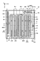
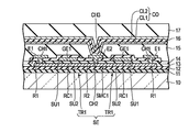
- FIG. 3 is a plan view showing the region. 4 is a cross-sectional view of the photosensor device of FIG. 3 taken along line IV-IV.
- FIG. 5 is a cross-sectional view of the photosensor device of FIG. 3 taken along line VV. 6 is a cross-sectional view of the optical sensor device of FIG. 3 taken along line VI-VI.
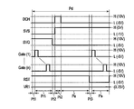
- FIG. 7 is a timing chart showing signals applied to each of the above regions.
- FIG. 1 is a circuit diagram showing an optical sensor device SD according to an embodiment.
- the first direction X, the second direction Y, and the third direction Z are orthogonal to each other, but may intersect at an angle other than 90 °.
- the first direction X and the second direction Y correspond to a direction parallel to the main surface of the substrate constituting the optical sensor device SD
- the third direction Z corresponds to the thickness direction of the optical sensor device SD.
- the optical sensor device SD includes an optical sensor panel SP, a control unit CN, and a wiring board CB.
- the wiring board CB is, for example, an FPC (flexible printed circuit), and connects the optical sensor panel SP and the control unit CN.
- the control unit CN includes a control circuit CC and a power supply circuit PO.
- the optical sensor panel SP includes an insulating substrate 10, a plurality of regions PX, a plurality of gate lines G (G1, G2,... Gn), a plurality of source lines S (S1, S2,... Sm), and the like.
- the insulating substrate 10 is made of an insulating material such as glass or resin. Furthermore, in the present embodiment, the insulating substrate 10 is formed of a transparent insulating material.
- the insulating substrate 10 has a detection area DA for detecting an object to be detected and a non-detection area NDA outside the detection area DA.
- the non-detection area NDA is a band-shaped first non-detection area NDA1 that is located on the left side of the detection area DA and extends in the second direction Y, and a band-like area that is located on the right side of the detection area DA and extends in the second direction Y.
- a strip-shaped fourth non-detection area NDA4 The plurality of regions PX are arranged in a matrix in the first direction X and the second direction Y on the detection region DA of the insulating substrate 10.
- the plurality of gate lines G extend in the first direction X and are arranged at intervals in the second direction Y in the detection area DA. Each gate line G is connected to a plurality of regions PX for one row arranged in the first direction X.
- the plurality of odd-numbered gate lines G are connected to the lead lines L extending through the first non-detection area NDA1 and the third non-detection area NDA3, respectively, outside the detection area DA.
- the plurality of even-numbered gate lines G are connected to lead lines L extending outside the detection area DA and extending through the second non-detection area NDA2 and the third non-detection area NDA3, respectively.
- Each lead wire L is connected to the wiring board CB. From the above, each gate line G is connected to the control circuit CC via the lead line L, the wiring board CB, and the like.
- the plurality of source lines S extend in the second direction Y and are arranged in the first direction X at intervals in the detection area DA.
- Each source line S is connected to a plurality of regions PX for one column arranged in the second direction Y.
- each source line S is routed in the third non-detection area NDA3 outside the detection area DA and connected to the wiring board CB.
- FIG. 2 is an equivalent circuit diagram showing the region PX shown in FIG. 1, and also shows the control circuit CC, the power supply circuit PO, and the selection switch SS shown in FIG.
- the region PX includes an optical sensor element SE, a capacitor CO, a reset switch RS, and a control switch CS. Further, on the insulating substrate 10 shown in FIG. 1, not only the gate line G and the source line S but also the first control wiring WL1, the second control wiring WL2, the third control wiring WL3, and the fourth control wiring WL4. Also arranged.
- FIG. 2 shows an example in which the optical sensor element SE is composed of one first thin film transistor TR1 for convenience.
- the photosensor element SE of the present embodiment is composed of a plurality of first thin film transistors TR1 connected in parallel to each other.
- the optical sensor element SE may be configured by only one first thin film transistor TR1.
- the first thin film transistor TR1 includes a first gate electrode GE1, a first electrode E1, and a second electrode E2.
- the first gate electrode GE1 is connected to the second control wiring WL2, and the first electrode E1 is connected to the first control wiring WL1.
- the first thin film transistor TR1 is turned on or off in response to a control signal SVG given through the second control wiring WL2.
- the capacitor CO has a first conductive layer CL1 and a second conductive layer CL2.
- the first conductive layer CL1 is connected to the second electrode E2, and the second conductive layer CL2 is connected to the third control wiring WL3.
- the reset switch RS is composed of a second thin film transistor TR2.
- the second thin film transistor TR2 includes a second gate electrode GE2, a third electrode E3, and a fourth electrode E4.
- the second gate electrode GE2 is connected to the fourth control line WL4, the third electrode E3 is connected to the third control line WL3 and the second conductive layer CL2, and the fourth electrode E4 is connected to the second electrode E2 and the first conductive layer CL1. It is connected to the.
- the second thin film transistor TR2 is turned on or off in response to the control signal DCH given through the fourth control wiring WL4.
- the control switch CS is composed of a third thin film transistor TR3.
- the third thin film transistor TR3 includes a third gate electrode GE3, a fifth electrode E5, and a sixth electrode E6.
- the third gate electrode GE3 is connected to the gate line G
- the fifth electrode E5 is connected to the source line S
- the sixth electrode E6 is connected to the second electrode E2, the fourth electrode E4, and the first conductive layer CL1. Yes.
- the third thin film transistor TR3 is turned on or off according to the control signal Gate given through the gate line G.
- the control unit CN includes not only the control circuit CC and the power supply circuit PO, but also a selection switch SS and a fifth control wiring WL5.
- the selection switch SS includes a fourth thin film transistor TR4 and a fifth thin film transistor TR5.
- the first thin film transistor TR1 to the fourth thin film transistor TR4 are N-channel thin film transistors
- the fifth thin film transistor TR5 is a P-channel thin film transistor.
- the fourth thin film transistor TR4 is connected between the source line S and the power supply circuit PO.
- the fifth thin film transistor TR5 is connected between the source line S and the control circuit CC.
- the fourth thin film transistor TR4 and the fifth thin film transistor TR5 are turned on or off in response to a control signal RST given through the fifth control wiring WL5.
- the selection switch SS supplies the reset signal VR1 from the power supply circuit PO to the photosensor element SE via the source line S and the control switch CS.
- the selection switch SS discharges the capacitor CO to the control circuit CC via the control switch CS and the source line S. As a result, a current I flows from the capacitor CO to the control circuit CC.
- the optical sensor element SE When the optical sensor element SE is turned on, the optical sensor element SE is reset by a reset signal VR1 given through the control switch CS. On the other hand, when the photosensor element SE is turned off, the photosensor element SE controls the amount of electric charge that flows through the first conductive layer CL1 in accordance with the amount of incident light. In other words, the optical sensor element SE controls the amount of the control signal SVS given to the first electrode E1 via the first control wiring WL1 to the first conductive layer CL1 according to the amount of incident light. Therefore, the optical sensor element SE controls the amount of charge charged in the capacitor CO according to the amount of incident light.
- the reset switch RS When the reset switch RS is turned on, the reset switch RS short-circuits the first conductive layer CL1 and the second conductive layer CL2. Note that a reset signal VR1 is applied to the third electrode E3 of the reset switch RS.
- the reset signal VR1 is a constant potential voltage signal.
- the reset switch RS When the reset switch RS is turned off, the reset switch RS maintains the original function of the capacitor CO. Therefore, the capacitor CO is reset when the reset switch RS is turned on.
- control switch CS When the control switch CS is turned on, the control switch CS switches whether to apply the reset signal VR1 to the photosensor element SE. Alternatively, when the control switch CS is turned on, the control switch CS switches whether to discharge from the capacitor CO to the control circuit CC.
- FIG. 3 is a plan view showing the region PX shown in FIG. In FIG. 3, the second conductive layer CL2 is not shown.
- the first conductive layer CL1 (capacitor CO) covers the optical sensor element SE, the reset switch RS, and the control switch CS.
- the first conductive layer CL1 functions as a common node for the photosensor element SE, the reset switch RS, and the control switch CS. Therefore, compared to the case where the first conductive layer CL1 does not function as the node, the area efficiency of the photosensor element SE, the reset switch RS, and the control switch CS in the region PX can be increased. For example, the wiring connecting the optical sensor element SE, the reset switch RS, and the control switch CS can be reduced, and the arrangement area of the optical sensor element SE and the like can be increased.
- the exclusive area of the optical sensor element SE is the largest.
- the optical sensor element SE occupies 50% or more of the region facing the first conductive layer CL1. Therefore, a highly sensitive photosensor element SE can be obtained.
- the optical sensor element SE has, for example, striped first electrodes E1 that extend in the second direction Y and are provided at intervals in the first direction X.
- the plurality of first electrodes E1 are electrically bundled with the first control wiring WL1.
- the first electrode E1 and the first control wiring WL1 are integrally formed.
- the optical sensor element SE has a plurality of second electrodes E2. Each second electrode E2 extends in the second direction Y and is positioned between the first electrodes E1. In the illustrated example, in the region between a pair of adjacent first electrodes E1, the upper second electrode E2 and the lower second electrode E2 are positioned with an insulation distance. Each second electrode E2 is connected to the first conductive layer CL1. In the illustrated example, the optical sensor element SE includes 24 first thin film transistors TR1 connected in parallel to each other.
- the optical sensor element SE has, for example, a stripe-shaped first gate electrode GE1 that extends in the second direction Y and is provided at intervals in the first direction X.
- the plurality of first gate electrodes GE1 are electrically bundled with the second control wiring WL2.
- the optical sensor element SE has, for example, a plurality of first semiconductor layers SMC1.
- the two first semiconductor layers SMC1 are physically arranged independently.
- three or more first semiconductor layers SMC1 may be physically arranged in the second direction Y independently.
- the single first semiconductor layer SMC1 may extend continuously in the second direction Y. In other words, the first semiconductor layer SMC1 may not be divided into a plurality of parts in the second direction Y.
- the third electrode E3 is formed integrally with, for example, the third control wiring WL3 extending in the first direction X and extending in the second direction Y.
- the fourth electrode E4 extends in the first direction X and is connected to the first conductive layer CL1.
- the second gate electrode GE2 extends in the first direction X, is located between the third electrode E3 and the fourth electrode E4, and is electrically connected to the fourth control wiring WL4 extending in the second direction Y.
- the first light shielding layer SH1 is opposed to the second gate electrode GE2, and extends along the second gate electrode GE2.
- the fifth electrode E5 extends in the second direction Y and is formed integrally with the source line S extending in the second direction Y.
- the sixth electrode E6 extends in the second direction Y and is connected to the first conductive layer CL1.
- the third gate electrode GE3 extends in the second direction Y, is located between the fifth electrode E5 and the sixth electrode E6, and is integrally formed with the gate line G extending in the first direction X. .
- the second light shielding layer SH2 faces the third gate electrode GE3 and extends along the third gate electrode GE3.
- the third semiconductor layer SMC3 of the control switch CS extends continuously in the second direction Y.
- the control switch CS may include a plurality of third semiconductor layers SMC3 that are physically arranged in the second direction Y independently.
- the first light shielding layer SH1 and the second light shielding layer SH2 described above are formed of the same material.
- the gate line G, the first gate electrode GE1, the second gate electrode GE2, and the third gate electrode GE3 described above are formed of the same material.
- the first electrode E1 to the sixth electrode E6, the source line S, and the first control wiring WL1 to the fourth control wiring WL4 described above are formed of the same material.
- FIG. 4 is a cross-sectional view of the optical sensor device SD of FIG. 3 taken along line IV-IV.
- a glass substrate can be used as the insulating substrate 10.
- a substrate other than a glass substrate may be used for the insulating substrate 10.
- the insulating substrate 10 may be a resin substrate.
- the insulating substrate 10 should just have a light transmittance as needed.
- an optical sensor element SE having a first gate electrode GE1, a first semiconductor layer SMC1, a first electrode E1, and a second electrode E2 is located above the insulating substrate 10.
- the optical sensor element SE is composed of a plurality of first thin film transistors TR1, and each first thin film transistor TR1 includes a first gate electrode GE1, a first semiconductor layer SMC1, a first electrode E1, and a second electrode E2.
- a capacitor CO having a first conductive layer CL1 and a second conductive layer CL2 is located above the photosensor element SE.
- the insulating layer 11 is disposed on the insulating substrate 10 and is in contact with the insulating substrate 10.
- the insulating layer 12 is disposed on the insulating layer 11 and is in contact with the insulating layer 11.
- the first gate electrode GE1 is disposed above the insulating substrate 10.
- the insulating layer 13 is disposed between the first gate electrode GE1 and the first semiconductor layer SMC1.
- the insulating layer 14 is disposed above the first gate electrode GE 1, the first semiconductor layer SMC 1, and the first insulating layer 13.
- the insulating layer 15 is disposed on the insulating layer 14, the first electrode E1, and the second electrode E2.
- the first semiconductor layer SMC1 is formed of an oxide semiconductor.
- the oxide semiconductor include, for example, indium gallium zinc oxide (IGZO), indium gallium oxide (IGO), indium zinc oxide (IZO), zinc tin oxide (ZnSnO), and zinc oxide (ZnO).
- IGZO indium gallium zinc oxide
- IGO indium gallium oxide
- IZO indium gallium oxide
- ZnSnO zinc tin oxide
- ZnO zinc oxide
- TAOS transparent amorphous oxide semiconductor
- the first semiconductor layer SMC1 is formed of TAOS.
- the first thin film transistor TR1 has a small current (leakage current) in a dark state and a large SN ratio.
- the first semiconductor layer SMC1 has a first region R1, a second region R2, and a first channel region RC1 located between the first region R1 and the second region R2.
- the first channel region RC1 includes a first main surface SU1 facing the first gate electrode GE1 and a second main surface SU2 opposite to the first main surface SU1.
- the electric resistance value changes according to the amount of light received by the second main surface SU2.
- the second main surface SU2 of the present embodiment faces the insulating substrate 10. Light transmitted through the insulating substrate 10 is incident on the second main surface SU2. Therefore, the insulating substrate 10 of this embodiment has light transmittance.
- the first electrode E1 is disposed on the insulating layer 14.
- the first electrode E1 passes through at least the insulating layer 14 and passes through the first contact hole CH1 located in a region facing the first region R1, and is electrically connected to the first region R1.
- the first contact hole CH1 penetrates the insulating layer 13 and the insulating layer 14.
- the second electrode E2 is disposed on the insulating layer 14.
- the second electrode E2 passes through at least the insulating layer 14 and passes through the second contact hole CH2 located in a region facing the second region R2, and is electrically connected to the second region R2.
- the second contact hole CH2 penetrates the insulating layer 13 and the insulating layer 14.
- the first conductive layer CL1 is disposed above the insulating layer 15 and covers the photosensor element SE. In the present embodiment, the first conductive layer CL1 is in contact with the insulating layer 15. The first conductive layer CL1 passes through at least the insulating layer 15 and passes through the third contact hole CH3 located in a region facing the second electrode E2, and is electrically connected to the second electrode E2. In the present embodiment, only the insulating layer 15 penetrates the third contact hole CH3.
- a plurality of third contact holes CH3 having the same configuration are formed in the insulating layer 15 (FIG. 3).
- the number of third contact holes CH3 is equal to or greater than the number of second electrodes E2. From the above, the first conductive layer CL1 passes through one corresponding third contact hole CH3 among the plurality of third contact holes CH3, and is electrically connected to the second electrode E2 of each first thin film transistor TR1. ing.
- the insulating layer 16 is disposed on the insulating layer 15 and the first conductive layer CL1, and is in contact with the insulating layer 15 and the first conductive layer CL1.
- the second conductive layer CL2 is opposed to the first conductive layer CL1.
- the second conductive layer CL2 faces the plurality of first conductive layers CL1.
- the insulating layer 16 is disposed between the first conductive layer CL1 and the second conductive layer CL2.
- the first conductive layer CL1 is disposed between the insulating layer 15 and the second conductive layer CL2. Therefore, the second conductive layer CL2 can avoid a situation in which an adverse electrical influence such as static electricity is applied to the first conductive layer CL1.
- the insulating layer 17 is disposed on the insulating layer 16 and the second conductive layer CL2, and is in contact with the insulating layer 16 and the second conductive layer CL2.
- the first gate electrode GE1, the first electrode E1, and the second electrode E2 are made of, for example, molybdenum, chromium, tungsten, aluminum, copper, titanium, nickel, tantalum, silver, or an alloy thereof, but are particularly limited. However, it may be formed of other metals or alloys, or a laminated film thereof.
- the first conductive layer CL1 and the second conductive layer CL2 are formed of a light transmissive conductive material such as ITO. Therefore, the optical sensor panel SP can be formed by a manufacturing method similar to that of a liquid crystal display panel in FFS (Fringe / Field / Switching) mode.
- the first conductive layer CL1 and the second conductive layer CL2 may be formed using a light-shielding conductive material such as metal. If not, the optical sensor element SE is for detecting light transmitted through the insulating substrate 10.
- the insulating layer 11, the insulating layer 12, the insulating layer 13, the insulating layer 14, and the insulating layer 16 are formed of an inorganic insulating layer such as silicon oxide or silicon nitride, or a laminate thereof.
- the insulating layer 15 and the insulating layer 17 are formed of an organic insulating layer.
- FIG. 5 is a cross-sectional view showing the optical sensor device SD of FIG. 3 along the line VV.
- the reset switch RS having the second gate electrode GE2, the second semiconductor layer SMC2, the third electrode E3, and the fourth electrode E4 is located above the insulating substrate 10.
- the reset switch RS is composed of a second thin film transistor TR2.
- a capacitor CO is located above the reset switch RS.
- the insulating layer 12 is located between the first light shielding layer SH1 and the second semiconductor layer SMC2.
- the second gate electrode GE2 is formed above the insulating substrate 10.
- the second semiconductor layer SMC2 is formed of, for example, TAOS as an oxide semiconductor.
- the second semiconductor layer SMC2 has a third region R3, a fourth region R4, and a second channel region RC2 located between the third region R3 and the fourth region R4.
- the second channel region RC2 includes a third main surface SU3 that faces the second gate electrode GE2, and a fourth main surface SU4 that is located on the opposite side of the third main surface SU3 and faces the first light shielding layer SH1. Contains.
- the insulating layer 13 is further disposed between the second gate electrode GE2 and the second semiconductor layer SMC2.
- the insulating layer 14 is further disposed above the first light shielding layer SH1, the second gate electrode GE2, and the second semiconductor layer SMC2.
- the third electrode E3 is disposed on the insulating layer 14.
- the third electrode E3 passes through at least the insulating layer 14 and passes through the fourth contact hole CH4 located in a region facing the third region R3, and is electrically connected to the third region R3.
- the fourth contact hole CH4 penetrates the insulating layer 13 and the insulating layer 14.
- the fourth electrode E4 is disposed on the insulating layer 14.
- the fourth electrode E4 passes through at least the insulating layer 14 and passes through the fifth contact hole CH5 located in a region facing the fourth region R4, and is electrically connected to the fourth region R4.
- the fifth contact hole CH5 penetrates the insulating layer 13 and the insulating layer 14.
- the first conductive layer CL1 covers the reset switch RS.
- the first conductive layer CL1 passes through at least the insulating layer 15 and passes through the sixth contact hole CH6 located in a region facing the fourth electrode E4, and is electrically connected to the fourth electrode E4. In the present embodiment, only the insulating layer 15 penetrates the sixth contact hole CH6.
- the second conductive layer CL2 passes through at least the insulating layer 15 and passes through the seventh contact hole CH7 located in a region facing the third electrode E3, and is electrically connected to the third electrode E3.
- the seventh contact hole CH7 penetrates the insulating layer 15 and the insulating layer 16.
- the first conductive layer CL1 has an opening OP and surrounds the seventh contact hole CH7.
- FIG. 6 is a cross-sectional view of the optical sensor device SD of FIG. 3 taken along line VI-VI.
- a control switch CS having a third gate electrode GE3, a third semiconductor layer SMC3, a fifth electrode E5, and a sixth electrode E6 is located above the insulating substrate 10.
- the control switch CS is composed of a third thin film transistor TR3.
- a capacitor CO is located above the control switch CS.
- the insulating layer 12 is further located between the second light shielding layer SH2 and the third semiconductor layer SMC3.
- the third gate electrode GE3 is disposed above the insulating substrate 10.
- the third semiconductor layer SMC3 is formed of, for example, TAOS as an oxide semiconductor.
- the third semiconductor layer SMC3 includes a fifth region R5, a sixth region R6, and a third channel region RC3 located between the fifth region R5 and the sixth region R6.
- the third channel region RC3 includes a fifth main surface SU5 that faces the third gate electrode GE3, and a sixth main surface SU6 that faces the second light shielding layer SH2 and is located on the opposite side of the fifth main surface SU5. Contains.
- the insulating layer 13 is further disposed between the third gate electrode GE3 and the third semiconductor layer SMC3.
- the insulating layer 14 is further disposed above the second light shielding layer SH2, the third gate electrode GE3, and the third semiconductor layer SMC3.
- the fifth electrode E5 is disposed on the insulating layer 14.
- the fifth electrode E5 passes through at least the insulating layer 14 and passes through the eighth contact hole CH8 located in a region facing the fifth region R5, and is electrically connected to the fifth region R5.
- the eighth contact hole CH8 penetrates the insulating layer 13 and the insulating layer 14.
- the sixth electrode E6 is disposed on the insulating layer 14.
- the sixth electrode E6 passes through at least the insulating layer 14 and passes through the ninth contact hole CH9 located in a region facing the sixth region R6, and is electrically connected to the sixth region R6.
- the ninth contact hole CH9 penetrates the insulating layer 13 and the insulating layer 14.
- the first conductive layer CL1 covers the control switch CS.
- the first conductive layer CL1 passes through at least the insulating layer 15 and passes through the tenth contact hole CH10 located in a region facing the sixth electrode E6, and is electrically connected to the sixth electrode E6. In the present embodiment, only the insulating layer 15 penetrates the tenth contact hole CH10.
- the optical sensor device SD of the present embodiment is configured.
- FIG. 7 is a timing chart showing signals applied to each of the regions PX.
- the detection period Pd is a period in which the detection operation for detecting the detection object in the detection area DA of the optical sensor panel SP is performed once.
- the detection period Pd has a first transition period Pt1, a first reset period Pr1, a second transition period Pt2, a second reset period Pr2, an exposure period Pe, a third transition period Pt3, and a readout period Pa.
- the control unit CN switches the level of the control signal SVS from the H (high) level to the L (low) level, and switches the level of the control signal SVG from the L level to the H level.
- the first electrode E1 of the photosensor element SE transitions to the L level ( ⁇ 1V)
- the first gate electrode GE1 transitions to the H level (10V).
- the voltage values used in the present embodiment are examples and can be variously modified.
- the control unit CN gives the control signal Gate (1),... Gate (n) of the H level (10V) to each gate line G, and then the control signal Gate ( 1)... Gate (n) level is switched from H level to L level ( ⁇ 5V). Since the first reset period Pr1 has a period after the level of the control signal Gate is switched from the H level to the L level, the potential of the third gate electrode GE3 of the control switch CS can be changed to substantially 10V. it can.
- the plurality of gate lines G are driven in a time division manner. Specifically, after the level of the control signal Gate (1) applied to the gate line G1 is switched from H level to L level, the level of the control signal Gate applied to the gate line G2 is switched from L level to H level. Next, the level of the control signal Gate applied to the gate line G2 is switched from the H level to the L level, and then the level of the control signal Gate applied to the gate line G3 is switched from the L level to the H level. Finally, the level of the control signal Gate (n) applied to the gate line Gn is switched from the H level to the L level.
- the control unit CN switches the level of the control signal SVG from the H level to the L level. Accordingly, in the second transition period Pt2, the first gate electrode GE1 of the photosensor element SE transits to the L level, and the photosensor element SE is turned off.
- the control unit CN switches the level of the control signal DCH from the L level ( ⁇ 5V) to the H level (10V), and changes the level of the control signal SVS from the L level to the H level. Switch.
- the reset switch RS is turned on, the reset signal VR1 is supplied to the first conductive layer CL1 and the second conductive layer CL2 via the third control wiring WL3, and the capacitor CO is reset.
- the control unit CN switches the level of the control signal DCH from the H level to the L level.
- the reset switch RS is turned off.
- the optical sensor element SE controls the amount of the H level control signal SVS applied to the first electrode E1 through the first control wiring WL1 to the first conductive layer CL1 according to the amount of incident light.
- the greater the amount of light incident on the photosensor element SE the greater the amount of charge charged on the capacitor CO.
- the second semiconductor layer SMC2 of the reset switch RS is shielded from light by the first light shielding layer SH1
- the third semiconductor layer SMC3 of the control switch CS is shielded from light by the second light shielding layer SH2. Therefore, the reset switch RS and the control switch CS are always in a dark state.
- the control unit CN switches the level of the control signal RST from the H level (10V) to the L level ( ⁇ 5V).
- the fourth thin film transistor TR4 is switched to the off state, and the fifth thin film transistor TR5 is switched to the on state.
- the control unit CN gives the H level control signals Gate (1),... Gate (n) to each gate line G, and then the control signals Gate (1),.
- the level of (n) is switched from the H level to the L level. Since the read period Pa has a period after the level of the control signal Gate is switched from the H level to the L level, the potential of the third gate electrode GE3 of the control switch CS can be changed to substantially 10V.
- the plurality of gate lines G are driven in a time division manner.
- an H level control signal Gate is applied through the gate line G corresponding to each control switch CS, the control switch CS is turned on. Then, discharging from the capacitor CO to the control circuit CC is performed. As a result, a current I flows from the capacitor CO to the control circuit CC.
- the plurality of gate lines G may be simultaneously driven at the same time. Thereby, the reading period Pa can be shortened.
- the optical sensor device SD includes the insulating substrate 10, the plurality of regions PX arranged in a matrix above the insulating substrate 10, and the first 1 conductive layer CL1.
- the region PX includes an optical sensor element SE, a reset switch RS, and a control switch CS.
- the optical sensor element SE, the reset switch RS, and the control switch CS are each connected to the first conductive layer CL1 and covered with the first conductive layer CL1. Therefore, the arrangement area of the optical sensor element SE, the reset switch RS, and the control switch CS in the region PX can be increased.
- the second conductive layer CL2 covers the first conductive layer CL1. Therefore, the capacitor CO can be formed using the first conductive layer CL1 and the second conductive layer CL2. Further, the second conductive layer CL2 can avoid a situation in which an adverse electrical effect such as static electricity is exerted on the first conductive layer CL1. From the above, a highly sensitive photosensor element SE can be obtained.
- the thin film transistor TR such as the first thin film transistor TR1 may be a bottom gate type thin film transistor instead of a top gate type thin film transistor.
- the second main surface SU2 of the first channel region RC1 of the first semiconductor layer SMC1 faces the first conductive layer CL1.
- Light transmitted through the first conductive layer CL1 and the like is incident on the second main surface SU2.
- the first conductive layer CL1 and the second conductive layer CL2 have light transmittance
- the insulating substrate 10 may not have light transmittance.
- the positional relationship between the first conductive layer CL1 and the second conductive layer CL2 may be opposite to that in the above embodiment.
- the second conductive layer CL2 is located between the insulating substrate 10 and the first conductive layer CL1.
- the first conductive layer CL1 does not have the opening OP
- the second conductive layer CL2 has an opening for connecting the first conductive layer CL1 to the third electrode E3 (third control wiring WL3). doing.
- the first light shielding layer SH1 and the second light shielding layer SH2 may be formed of an insulating material such as a black resin or a conductive material such as a metal.
- the light shielding layer SH may be in an electrically floating state.
- the light shielding layer SH may be given to the control signal Gate, and the light shielding layer SH may be used as a gate electrode.
Landscapes
- Engineering & Computer Science (AREA)
- Multimedia (AREA)
- Signal Processing (AREA)
- Solid State Image Pick-Up Elements (AREA)
- Thin Film Transistor (AREA)
- Transforming Light Signals Into Electric Signals (AREA)
Abstract
光センサ装置は、絶縁基板と、第1導電層と、前記絶縁基板と前記第1導電層との間に配置された光センサ素子と、を備える。前記光センサ素子は、前記第1導電層に電気的に接続され、前記第1導電層で覆われている。前記光センサ素子は、酸化物半導体で形成された第1半導体層を有し、入射される光の光量に応じて前記第1導電層に流す電荷の量を制御する。
Description
本発明の実施形態は、光センサ装置に関する。
光センサ装置として、例えばCMOSイメージセンサが知られている。CMOSイメージセンサは、複数の領域を有している。CMOSイメージセンサは、多結晶シリコンで形成された半導体層を利用して形成されている。領域の低精細化及び領域の大面積化に、CMOSイメージセンサは向いていない。そのため、CMOSイメージセンサを使用する場合、さらに光学系を使用し、CMOSイメージセンサの領域に集光する必要がる。
本実施形態は、高感度の光センサ装置を提供する。
一実施形態に係る光センサ装置は、
絶縁基板と、第1ゲート電極、第1半導体層、第1電極、及び第2電極を有する光センサ素子と、前記第1ゲート電極と前記第1半導体層との間に配置された第1絶縁層と、前記第1ゲート電極、前記第1半導体層、及び前記第1絶縁層の上方に配置された第2絶縁層と、前記第2絶縁層、前記第1電極、及び前記第2電極の上に配置された第3絶縁層と、前記光センサ素子を覆った第1導電層と、を備え、前記第1ゲート電極は、前記絶縁基板の上方に形成され、前記第1半導体層は、酸化物半導体で形成され、第1領域と、第2領域と、前記第1領域と前記第2領域との間に位置した第1チャネル領域と、を有し、前記第1チャネル領域は、前記第1ゲート電極と対向した第1主面と前記第1主面とは反対側の第2主面とを含み、前記第2主面で受ける光の光量に応じて電気抵抗値が変化し、前記第1電極は、前記第2絶縁層の上に配置され、少なくとも前記第2絶縁層を貫通し前記第1領域と対向する領域に位置した第1コンタクトホールを通って前記第1領域に電気的に接続され、前記第2電極は、前記第2絶縁層の上に配置され、少なくとも前記第2絶縁層を貫通し前記第2領域と対向する領域に位置した第2コンタクトホールを通って前記第2領域に電気的に接続され、前記第1導電層は、前記第3絶縁層の上方に配置され、少なくとも前記第3絶縁層を貫通し前記第2電極と対向する領域に位置した第3コンタクトホールを通って前記第2電極に電気的に接続されている。
絶縁基板と、第1ゲート電極、第1半導体層、第1電極、及び第2電極を有する光センサ素子と、前記第1ゲート電極と前記第1半導体層との間に配置された第1絶縁層と、前記第1ゲート電極、前記第1半導体層、及び前記第1絶縁層の上方に配置された第2絶縁層と、前記第2絶縁層、前記第1電極、及び前記第2電極の上に配置された第3絶縁層と、前記光センサ素子を覆った第1導電層と、を備え、前記第1ゲート電極は、前記絶縁基板の上方に形成され、前記第1半導体層は、酸化物半導体で形成され、第1領域と、第2領域と、前記第1領域と前記第2領域との間に位置した第1チャネル領域と、を有し、前記第1チャネル領域は、前記第1ゲート電極と対向した第1主面と前記第1主面とは反対側の第2主面とを含み、前記第2主面で受ける光の光量に応じて電気抵抗値が変化し、前記第1電極は、前記第2絶縁層の上に配置され、少なくとも前記第2絶縁層を貫通し前記第1領域と対向する領域に位置した第1コンタクトホールを通って前記第1領域に電気的に接続され、前記第2電極は、前記第2絶縁層の上に配置され、少なくとも前記第2絶縁層を貫通し前記第2領域と対向する領域に位置した第2コンタクトホールを通って前記第2領域に電気的に接続され、前記第1導電層は、前記第3絶縁層の上方に配置され、少なくとも前記第3絶縁層を貫通し前記第2電極と対向する領域に位置した第3コンタクトホールを通って前記第2電極に電気的に接続されている。
また、一実施形態に係る光センサ装置は、
絶縁基板と、前記絶縁基板の上方に配置された第1導電層と、前記絶縁基板と前記第1導電層との間に配置され、前記第1導電層に電気的に接続され、前記第1導電層で覆われ、酸化物半導体で形成された第1半導体層を有し、入射される光の光量に応じて前記第1導電層に流す電荷の量を制御する光センサ素子と、を備える。
絶縁基板と、前記絶縁基板の上方に配置された第1導電層と、前記絶縁基板と前記第1導電層との間に配置され、前記第1導電層に電気的に接続され、前記第1導電層で覆われ、酸化物半導体で形成された第1半導体層を有し、入射される光の光量に応じて前記第1導電層に流す電荷の量を制御する光センサ素子と、を備える。
また、一実施形態に係る光センサ装置は、
絶縁基板と、前記絶縁基板の上方にマトリクス状に配置された複数の領域と、を備え、各々の前記領域は、前記絶縁基板の上方に配置された第1導電層と、前記絶縁基板と前記第1導電層との間に配置され、前記第1導電層に電気的に接続され、前記第1導電層で覆われ、酸化物半導体で形成された第1半導体層を有し、入射される光の光量に応じて前記第1導電層に流す電荷の量を制御する光センサ素子と、を有する。
絶縁基板と、前記絶縁基板の上方にマトリクス状に配置された複数の領域と、を備え、各々の前記領域は、前記絶縁基板の上方に配置された第1導電層と、前記絶縁基板と前記第1導電層との間に配置され、前記第1導電層に電気的に接続され、前記第1導電層で覆われ、酸化物半導体で形成された第1半導体層を有し、入射される光の光量に応じて前記第1導電層に流す電荷の量を制御する光センサ素子と、を有する。
以下に、本発明の一実施の形態について、図面を参照しつつ説明する。なお、開示はあくまで一例にすぎず、当業者において、発明の主旨を保っての適宜変更について容易に想到し得るものについては、当然に本発明の範囲に含有されるものである。また、図面は説明をより明確にするため、実際の態様に比べ、各部の幅、厚さ、形状等について模式的に表される場合があるが、あくまで一例であって、本発明の解釈を限定するものではない。また、本明細書と各図において、既出の図に関して前述したものと同様の要素には、同一の符号を付して、詳細な説明を適宜省略することがある。
図1は、一実施形態に係る光センサ装置SDを示す回路図である。第1方向X、第2方向Y及び第3方向Zは、互いに直交しているが、90°以外の角度で交差していてもよい。第1方向X及び第2方向Yは、光センサ装置SDを構成する基板の主面と平行な方向に相当し、第3方向Zは、光センサ装置SDの厚さ方向に相当する。
図1に示すように、光センサ装置SDは、光センサパネルSPと、制御部CNと、配線基板CBと、を備えている。配線基板CBは、例えばFPC(flexible printed circuit)であり、光センサパネルSPと制御部CNとを連結している。制御部CNは、制御回路CC及び電源回路POを備えている。
光センサパネルSPは、絶縁基板10、複数の領域PX、複数のゲート線G(G1、G2、…Gn)、複数のソース線S(S1、S2、…Sm)などを備えている。絶縁基板10は、ガラスや、樹脂などの絶縁材料で形成されている。さらに、本実施形態において、絶縁基板10は、透明な絶縁材料で形成されている。絶縁基板10は、被検出物を検出する検出領域DAと、検出領域DAの外側の非検出領域NDAと、を有している。非検出領域NDAは、検出領域DAの左側に位置し第2方向Yに延在した帯状の第1非検出領域NDA1と、検出領域DAの右側に位置し第2方向Yに延在した帯状の第2非検出領域NDA2と、検出領域DAの下側に位置し第1方向Xに延在した帯状の第3非検出領域NDA3と、検出領域DAの上側に位置し第1方向Xに延在した帯状の第4非検出領域NDA4と、を有している。複数の領域PXは、絶縁基板10の検出領域DA上に、第1方向X及び第2方向Yにマトリクス状に配置されている。
複数のゲート線Gは、検出領域DAにて、第1方向Xに延在し、第2方向Yに間隔を置いて並んでいる。各々のゲート線Gは、第1方向Xに並んだ一行分の複数の領域PXに接続されている。本実施形態において、奇数行の複数のゲート線Gは、検出領域DAの外側において、それぞれ、第1非検出領域NDA1及び第3非検出領域NDA3を延在するリード線Lに接続されている。偶数行の複数のゲート線Gは、検出領域DAの外側において、それぞれ、第2非検出領域NDA2及び第3非検出領域NDA3を延在するリード線Lに接続されている。各々のリード線Lは、配線基板CBに接続されている。上記のことから、各々のゲート線Gは、リード線L、配線基板CBなどを介して制御回路CCに接続されている。
複数のソース線Sは、検出領域DAにて、第2方向Yに延在し、第1方向Xに間隔を置いて並んでいる。各々のソース線Sは、第2方向Yに並んだ一列分の複数の領域PXに接続されている。本実施形態において、各々のソース線Sは、検出領域DAの外側において、第3非検出領域NDA3にて引き回され、配線基板CBに接続されている。
次に、上記複数の領域PXを代表し、一領域PXについて説明する。なお、複数の領域PXは、同様に構成されている。図2は、図1に示した領域PXを示す等価回路図であり、図1に示した制御回路CC及び電源回路PO、並びに選択スイッチSSを併せて示す図である。
図2に示すように、領域PXは、光センサ素子SEと、コンデンサCOと、リセットスイッチRSと、制御スイッチCSと、を備えている。また、図1に示した絶縁基板10の上には、ゲート線G及びソース線Sだけではなく、第1制御配線WL1、第2制御配線WL2、第3制御配線WL3、及び第4制御配線WL4も配置されている。
図2では、便宜的に、光センサ素子SEが1個の第1薄膜トランジスタTR1で構成されている例を示している。但し、後述するように、本実施形態の光センサ素子SEは、互いに並列に接続された複数個の第1薄膜トランジスタTR1で構成されている。なお、本実施形態と異なり、光センサ素子SEは、1個の第1薄膜トランジスタTR1のみで構成されていてもよい。
第1薄膜トランジスタTR1は、第1ゲート電極GE1、第1電極E1、及び第2電極E2を有している。第1ゲート電極GE1は第2制御配線WL2に接続され、第1電極E1は第1制御配線WL1に接続されている。第1薄膜トランジスタTR1は、第2制御配線WL2を介して与えられる制御信号SVGに応じてオン又はオフする。
コンデンサCOは、第1導電層CL1及び第2導電層CL2を有している。第1導電層CL1は第2電極E2に接続され、第2導電層CL2は第3制御配線WL3に接続されている。
リセットスイッチRSは、第2薄膜トランジスタTR2で構成されている。第2薄膜トランジスタTR2は、第2ゲート電極GE2、第3電極E3、及び第4電極E4を有している。第2ゲート電極GE2は第4制御配線WL4に接続され、第3電極E3は第3制御配線WL3及び第2導電層CL2に接続され、第4電極E4は第2電極E2及び第1導電層CL1に接続されている。第2薄膜トランジスタTR2は、第4制御配線WL4を介して与えられる制御信号DCHに応じてオン又はオフする。
制御スイッチCSは、第3薄膜トランジスタTR3で構成されている。第3薄膜トランジスタTR3は、第3ゲート電極GE3、第5電極E5、及び第6電極E6を有している。第3ゲート電極GE3はゲート線Gに接続され、第5電極E5はソース線Sに接続され、第6電極E6は第2電極E2、第4電極E4、及び第1導電層CL1に接続されている。第3薄膜トランジスタTR3は、ゲート線Gを介して与えられる制御信号Gateに応じてオン又はオフする。
制御部CNは、制御回路CC及び電源回路POだけではなく、選択スイッチSS及び第5制御配線WL5も備えている。選択スイッチSSは、第4薄膜トランジスタTR4及び第5薄膜トランジスタTR5を有している。本実施形態において、第1薄膜トランジスタTR1乃至第4薄膜トランジスタTR4はNチャネル型の薄膜トランジスタであり、第5薄膜トランジスタTR5はPチャネル型の薄膜トランジスタである。
第4薄膜トランジスタTR4は、ソース線Sと電源回路POとの間に接続されている。第5薄膜トランジスタTR5は、ソース線Sと制御回路CCとの間に接続されている。第4薄膜トランジスタTR4及び第5薄膜トランジスタTR5は、それぞれ第5制御配線WL5を介して与えられる制御信号RSTに応じてオン又はオフする。
第4薄膜トランジスタTR4がオンし、第5薄膜トランジスタTR5がオフした場合、選択スイッチSSは、ソース線S及び制御スイッチCSを介し、電源回路POから光センサ素子SEにリセット信号VR1を与える。一方、第4薄膜トランジスタTR4がオフし、第5薄膜トランジスタTR5がオンした場合、選択スイッチSSは、制御スイッチCS及びソース線Sを介し、コンデンサCOから制御回路CCへの放電を行う。これにより、コンデンサCOから制御回路CCに電流Iが流れる。
光センサ素子SEがオンした場合、光センサ素子SEは、制御スイッチCSを介して与えられるリセット信号VR1によりリセットされる。一方、光センサ素子SEがオフした場合、光センサ素子SEは、入射される光の光量に応じて第1導電層CL1に流す電荷の量を制御する。言い換えると、光センサ素子SEは、入射される光の光量に応じて、第1制御配線WL1を介して第1電極E1に与えられる制御信号SVSを第1導電層CL1に与える量を制御する。そのため、光センサ素子SEは、入射される光の光量に応じて、コンデンサCOに充電する電荷の量を制御する。
リセットスイッチRSがオンした場合、リセットスイッチRSは、第1導電層CL1と第2導電層CL2とを短絡させる。なお、リセットスイッチRSの第3電極E3には、リセット信号VR1が与えられている。リセット信号VR1は、定電位の電圧信号である。リセットスイッチRSがオフした場合、リセットスイッチRSは、コンデンサCOの本来の機能を維持する。そのため、コンデンサCOは、リセットスイッチRSがオンすることにより、リセットされる。
制御スイッチCSがオンした場合、制御スイッチCSは、リセット信号VR1を光センサ素子SEに与えるかどうか切り替える。又は、制御スイッチCSがオンした場合、制御スイッチCSは、コンデンサCOから制御回路CCへの放電を行うのかどうか切り替える。
図3は、図2に示した領域PXを示す平面図である。なお、図3において、第2導電層CL2の図示は省略している。
図3に示すように、第1導電層CL1(コンデンサCO)は、光センサ素子SE、リセットスイッチRS、及び制御スイッチCSを覆っている。第1導電層CL1は、光センサ素子SE、リセットスイッチRS、及び制御スイッチCSの共通のノードとして機能している。そのため、第1導電層CL1が上記ノードとして機能していない場合と比較して、領域PXにおける、光センサ素子SE、リセットスイッチRS、及び制御スイッチCSの面積効率を高くすることができる。例えば、光センサ素子SE、リセットスイッチRS、及び制御スイッチCSをつなぐ配線を減らすことができ、光センサ素子SEなどの配置面積を大きくとることができる。
光センサ素子SE、リセットスイッチRS、及び制御スイッチCSのうち、光センサ素子SEの専有面積は最も大きい。例えば、第1導電層CL1と対向する領域のうちの50%以上を光センサ素子SEが占めている。そのため、高感度の光センサ素子SEを得ることができる。
光センサ素子SEは、例えば、第2方向Yに延在し、第1方向Xに間隔を置いて設けられたストライプ状の第1電極E1を有している。複数の第1電極E1は、第1制御配線WL1に電気的に束ねられている。本実施形態において、第1電極E1及び第1制御配線WL1は、一体に形成されている。
光センサ素子SEは、複数の第2電極E2を有している。各々の第2電極E2は、第2方向Yに延在し、第1電極E1の間に位置している。図示した例では、隣り合う一対の第1電極E1の間の領域において、上側の第2電極E2と下側の第2電極E2は、絶縁距離を置いて位置している。各々の第2電極E2は、第1導電層CL1に接続されている。図示した例では、光センサ素子SEは、互いに並列に接続された24個の第1薄膜トランジスタTR1で構成されている。
光センサ素子SEは、例えば、第2方向Yに延在し、第1方向Xに間隔を置いて設けられたストライプ状の第1ゲート電極GE1を有している。複数の第1ゲート電極GE1は、第2制御配線WL2に電気的に束ねられている。
光センサ素子SEは、例えば、複数の第1半導体層SMC1を有している。第2方向Yに注目すると、2個の第1半導体層SMC1が、物理的に独立して並んでいる。但し、本実施形態と異なり、3個以上の第1半導体層SMC1が、第2方向Yに物理的に独立して並んでいてもよい。又は、単個の第1半導体層SMC1が、第2方向Yに連続的に延在していてもよい。言い換えると、第1半導体層SMC1は、第2方向Yに複数に分割されていなくともよい。
リセットスイッチRSにおいて、第3電極E3は、例えば、第1方向Xに延在し、第2方向Yに延在した第3制御配線WL3と一体に形成されている。第4電極E4は、例えば、第1方向Xに延在し、第1導電層CL1に接続されている。第2ゲート電極GE2は、第1方向Xに延在し、第3電極E3と第4電極E4との間に位置し、第2方向Yに延在した第4制御配線WL4に電気的に接続されている。第1遮光層SH1は、第2ゲート電極GE2と対向し、第2ゲート電極GE2に沿って延在している。
制御スイッチCSにおいて、第5電極E5は、例えば、第2方向Yに延在し、第2方向Yに延在したソース線Sと一体に形成されている。第6電極E6は、例えば、第2方向Yに延在し、第1導電層CL1に接続されている。第3ゲート電極GE3は、第2方向Yに延在し、第5電極E5と第6電極E6との間に位置し、第1方向Xに延在したゲート線Gと一体に形成されている。第2遮光層SH2は、第3ゲート電極GE3と対向し、第3ゲート電極GE3に沿って延在している。
制御スイッチCSの第3半導体層SMC3は、第2方向Yに連続的に延在している。但し、本実施形態と異なり、制御スイッチCSは、第2方向Yに物理的に独立して並んだ複数の第3半導体層SMC3を有していてもよい。
制御スイッチCSの第3半導体層SMC3は、第2方向Yに連続的に延在している。但し、本実施形態と異なり、制御スイッチCSは、第2方向Yに物理的に独立して並んだ複数の第3半導体層SMC3を有していてもよい。
上述した第1遮光層SH1及び第2遮光層SH2は、同一材料で形成されている。上述したゲート線G、第1ゲート電極GE1、第2ゲート電極GE2、及び第3ゲート電極GE3は、同一材料で形成されている。上述した第1電極E1乃至第6電極E6、ソース線S、及び第1制御配線WL1乃至第4制御配線WL4は、同一材料で形成されている。
次に、光センサ素子SE及びコンデンサCOの断面構造について説明する。図4は、図3の光センサ装置SDを線IV-IVに沿って示す断面図である。
図4に示すように、絶縁基板10としては、ガラス基板を利用することができる。但し、絶縁基板10にガラス基板以外の基板を利用してもよい。例えば、絶縁基板10は樹脂基板であってもよい。また、絶縁基板10は、必要に応じて光透過性を有していればよい。絶縁基板10の上方に、第1ゲート電極GE1、第1半導体層SMC1、第1電極E1、及び第2電極E2を有する光センサ素子SEが位置している。光センサ素子SEは複数の第1薄膜トランジスタTR1で構成され、各々の第1薄膜トランジスタTR1は、第1ゲート電極GE1、第1半導体層SMC1、第1電極E1、及び第2電極E2を含んでいる。光センサ素子SEの上方に、第1導電層CL1及び第2導電層CL2を有するコンデンサCOが位置している。
絶縁層11は、絶縁基板10の上に配置され、絶縁基板10に接している。絶縁層12は、絶縁層11の上に配置され、絶縁層11に接している。第1ゲート電極GE1は、絶縁基板10の上方に配置されている。絶縁層13は、第1ゲート電極GE1と第1半導体層SMC1との間に配置されている。絶縁層14は、第1ゲート電極GE1、第1半導体層SMC1、及び第1絶縁層13の上方に配置されている。絶縁層15は、絶縁層14、第1電極E1、及び第2電極E2の上に配置されている。
第1半導体層SMC1は、酸化物半導体で形成されている。酸化物半導体の代表的な例としては、例えば、酸化インジウムガリウム亜鉛(IGZO)、酸化インジウムガリウム(IGO)、インジウム亜鉛酸化物(IZO)、亜鉛スズ酸化物(ZnSnO)、亜鉛酸化物(ZnO)、及び透明アモルファス酸化物半導体(TAOS)などが挙げられる。本実施形態において、第1半導体層SMC1は、TAOSで形成されている。
上記のような酸化物半導体を利用すると、第1薄膜トランジスタTR1は、暗状態での電流(リーク電流)が小さくSN比を大きく取ることができる。
第1半導体層SMC1は、第1領域R1と、第2領域R2と、第1領域R1と第2領域R2との間に位置した第1チャネル領域RC1と、を有している。第1チャネル領域RC1は、第1ゲート電極GE1と対向した第1主面SU1と、第1主面SU1とは反対側の第2主面SU2とを含んでいる。第1チャネル領域RC1は、第2主面SU2で受ける光の光量に応じて電気抵抗値が変化する。
本実施形態の第2主面SU2は、絶縁基板10と対向している。第2主面SU2には、絶縁基板10を透過した光が入射される。そのため、本実施形態の絶縁基板10は、光透過性を有している。
第1電極E1は、絶縁層14の上に配置されている。第1電極E1は、少なくとも絶縁層14を貫通し第1領域R1と対向する領域に位置した第1コンタクトホールCH1を通り、第1領域R1に電気的に接続されている。本実施形態において、第1コンタクトホールCH1は、絶縁層13及び絶縁層14を貫通している。
第2電極E2は、絶縁層14の上に配置されている。第2電極E2は、少なくとも絶縁層14を貫通し第2領域R2と対向する領域に位置した第2コンタクトホールCH2を通り、第2領域R2に電気的に接続されている。本実施形態において、第2コンタクトホールCH2は、絶縁層13及び絶縁層14を貫通している。
第1導電層CL1は、絶縁層15の上方に配置され、光センサ素子SEを覆っている。本実施形態において、第1導電層CL1は絶縁層15に接している。第1導電層CL1は、少なくとも絶縁層15を貫通し第2電極E2と対向する領域に位置した第3コンタクトホールCH3を通り、第2電極E2に電気的に接続されている。本実施形態において、第3コンタクトホールCH3は絶縁層15のみ貫通している。
なお、絶縁層15には、同様に構成された複数の第3コンタクトホールCH3が形成されている(図3)。第3コンタクトホールCH3の個数は、第2電極E2の個数以上である。上記のことから、第1導電層CL1は、複数の第3コンタクトホールCH3のうち対応する一の第3コンタクトホールCH3を通り、各々の第1薄膜トランジスタTR1の第2電極E2に電気的に接続されている。
絶縁層16は、絶縁層15及び第1導電層CL1の上に配置され、絶縁層15及び第1導電層CL1に接している。第2導電層CL2は、第1導電層CL1と対向している。全てを図示しないが、第2導電層CL2は、複数の第1導電層CL1と対向している。なお、絶縁層16は、第1導電層CL1と第2導電層CL2との間に配置されている。第1導電層CL1は、絶縁層15と第2導電層CL2との間に配置されている。そのため、第2導電層CL2は、静電気などの外部からの電気的な悪影響が第1導電層CL1におよぶ事態を回避することができる。
絶縁層17は、絶縁層16及び第2導電層CL2の上に配置され、絶縁層16及び第2導電層CL2に接している。
第1ゲート電極GE1、第1電極E1、及び第2電極E2は、例えば、モリブデン、クロム、タングステン、アルミニウム、銅、チタン、ニッケル、タンタル、銀あるいはこれらの合金によって形成されているが、特に限定されるものではなく、その他の金属や合金、またはこれらの積層膜で形成されていてもよい。
第1導電層CL1及び第2導電層CL2は、ITOなどの光透過性の導電材料によって形成されている。そのため、FFS(Fringe Field Switching)モードの液晶表示パネルと同様の製造方法にて、光センサパネルSPを形成することが可能である。なお、第1導電層CL1及び第2導電層CL2は、金属などの遮光性の導電材料を用いて形成されていてもよい。なせなら、光センサ素子SEは、絶縁基板10を透過した光を検出するためである。
絶縁層11、絶縁層12、絶縁層13、絶縁層14、及び絶縁層16は、シリコン酸化物やシリコン窒化物などの無機絶縁層、又はそれらの積層体で形成されている。絶縁層15、及び絶縁層17は、有機絶縁層で形成されている。
次に、リセットスイッチRS及びコンデンサCOの断面構造について説明する。図5は、図3の光センサ装置SDを線V-Vに沿って示す断面図である。
図5に示すように、絶縁基板10の上方に、第2ゲート電極GE2、第2半導体層SMC2、第3電極E3、及び第4電極E4を有するリセットスイッチRSが位置している。リセットスイッチRSは第2薄膜トランジスタTR2で構成されている。リセットスイッチRSの上方に、コンデンサCOが位置している。
絶縁層12は、第1遮光層SH1と第2半導体層SMC2との間に位置している。第2ゲート電極GE2は、絶縁基板10の上方に形成されている。第2半導体層SMC2は、酸化物半導体として例えばTAOSで形成されている。第2半導体層SMC2は、第3領域R3と、第4領域R4と、第3領域R3と第4領域R4との間に位置した第2チャネル領域RC2と、を有している。第2チャネル領域RC2は、第2ゲート電極GE2と対向した第3主面SU3と、第3主面SU3とは反対側に位置し第1遮光層SH1と対向した第4主面SU4と、を含んでいる。
絶縁層13は、第2ゲート電極GE2と第2半導体層SMC2との間にさらに配置されている。絶縁層14は、第1遮光層SH1、第2ゲート電極GE2、及び第2半導体層SMC2の上方にさらに配置されている。
第3電極E3は、絶縁層14の上に配置されている。第3電極E3は、少なくとも絶縁層14を貫通し第3領域R3と対向する領域に位置した第4コンタクトホールCH4を通り、第3領域R3に電気的に接続されている。本実施形態において、第4コンタクトホールCH4は、絶縁層13及び絶縁層14を貫通している。
第4電極E4は、絶縁層14の上に配置されている。第4電極E4は、少なくとも絶縁層14を貫通し第4領域R4と対向する領域に位置した第5コンタクトホールCH5を通り、第4領域R4に電気的に接続されている。本実施形態において、第5コンタクトホールCH5は、絶縁層13及び絶縁層14を貫通している。
第1導電層CL1は、リセットスイッチRSを覆っている。第1導電層CL1は、少なくとも絶縁層15を貫通し第4電極E4と対向する領域に位置した第6コンタクトホールCH6を通り、第4電極E4に電気的に接続されている。本実施形態において、第6コンタクトホールCH6は絶縁層15のみ貫通している。
第2導電層CL2は、少なくとも絶縁層15を貫通し第3電極E3と対向する領域に位置した第7コンタクトホールCH7を通り、第3電極E3に電気的に接続されている。本実施形態において、第7コンタクトホールCH7は絶縁層15及び絶縁層16を貫通している。なお、第1導電層CL1は開口OPを有し、第7コンタクトホールCH7を囲んでいる。
次に、制御スイッチCS及びコンデンサCOの断面構造について説明する。図6は、図3の光センサ装置SDを線VI-VIに沿って示す断面図である。
図6に示すように、絶縁基板10の上方に、第3ゲート電極GE3、第3半導体層SMC3、第5電極E5、及び第6電極E6を有する制御スイッチCSが位置している。制御スイッチCSは第3薄膜トランジスタTR3で構成されている。制御スイッチCSの上方に、コンデンサCOが位置している。
絶縁層12は、第2遮光層SH2と第3半導体層SMC3との間にさらに位置している。第3ゲート電極GE3は、絶縁基板10の上方に配置されている。第3半導体層SMC3は、酸化物半導体として例えばTAOSで形成されている。第3半導体層SMC3は、第5領域R5と、第6領域R6と、第5領域R5と第6領域R6との間に位置した第3チャネル領域RC3と、を有している。第3チャネル領域RC3は、第3ゲート電極GE3と対向した第5主面SU5と、第5主面SU5とは反対側に位置し第2遮光層SH2と対向した第6主面SU6と、を含んでいる。
絶縁層13は、第3ゲート電極GE3と第3半導体層SMC3との間にさらに配置されている。絶縁層14は、第2遮光層SH2、第3ゲート電極GE3、及び第3半導体層SMC3の上方にさらに配置されている。
第5電極E5は、絶縁層14の上に配置されている。第5電極E5は、少なくとも絶縁層14を貫通し第5領域R5と対向する領域に位置した第8コンタクトホールCH8を通り、第5領域R5に電気的に接続されている。本実施形態において、第8コンタクトホールCH8は、絶縁層13及び絶縁層14を貫通している。
第6電極E6は、絶縁層14の上に配置されている。第6電極E6は、少なくとも絶縁層14を貫通し第6領域R6と対向する領域に位置した第9コンタクトホールCH9を通り、第6領域R6に電気的に接続されている。本実施形態において、第9コンタクトホールCH9は、絶縁層13及び絶縁層14を貫通している。
第1導電層CL1は、制御スイッチCSを覆っている。第1導電層CL1は、少なくとも絶縁層15を貫通し第6電極E6と対向する領域に位置した第10コンタクトホールCH10を通り、第6電極E6に電気的に接続されている。本実施形態において、第10コンタクトホールCH10は絶縁層15のみ貫通している。
以上のように、本実施形態の光センサ装置SDは構成されている。
次に、本実施形態の光センサ装置SDの駆動方法について例示的に説明する。図7は、各々の上記領域PXに与える信号を示すタイミングチャートである。
図7及び図2に示すように、光センサパネルSPの検出領域DAにて被検出物を検出するための検出動作を1回行う期間を検出期間Pdとする。検出期間Pdは、第1遷移期間Pt1、第1リセット期間Pr1、第2遷移期間Pt2、第2リセット期間Pr2、露光期間Pe、第3遷移期間Pt3、及び読み出し期間Paを有している。
まず、第1遷移期間Pt1において、制御部CNは、制御信号SVSのレベルをH(ハイ)レベルからL(ロウ)レベルに切り替え、制御信号SVGのレベルをLレベルからHレベルに切り替える。これにより、第1遷移期間Pt1にて、光センサ素子SEの第1電極E1がLレベル(-1V)に遷移し、第1ゲート電極GE1がHレベル(10V)に遷移する。なお、本実施形態で用いる電圧値は例示であり、種々変形可能である。
続いて、第1リセット期間Pr1に移行すると、制御部CNは、各々のゲート線GにHレベル(10V)の制御信号Gate(1)、…Gate(n)を与えた後、制御信号Gate(1)、…Gate(n)のレベルをHレベルからLレベル(-5V)に切り替える。第1リセット期間Pr1は、制御信号GateのレベルがHレベルからLレベルに切り替わった後の期間を有しているため、制御スイッチCSの第3ゲート電極GE3の電位を実質10Vに遷移させることができる。
本実施形態において、複数のゲート線Gは時分割的に駆動されている。具体的には、ゲート線G1に与える制御信号Gate(1)のレベルをHレベルからLレベルに切替えた後、ゲート線G2に与える制御信号GateのレベルをLレベルからHレベルに切替える。次いで、ゲート線G2に与える制御信号GateのレベルをHレベルからLレベルに切替えた後、ゲート線G3に与える制御信号GateのレベルをLレベルからHレベルに切替える。最後に、ゲート線Gnに与える制御信号Gate(n)のレベルをHレベルからLレベルに切替える。
各々の制御スイッチCSに対応するゲート線Gを介してHレベルの制御信号Gateが与えられると、制御スイッチCSはオンし、選択スイッチSS及びソース線Sを介して電源回路POから出力されるリセット信号VR1を光センサ素子SEに与える。は、ソース線S及び制御スイッチCSを介し、電源回路POから光センサ素子SEにリセット信号VR1を与える。そして、リセット信号VR1が光センサ素子SEの第2電極E2から第1電極E1に流れることで、光センサ素子SEはリセットされる。
その後、第2遷移期間Pt2に移行すると、制御部CNは、制御信号SVGのレベルをHレベルからLレベルに切り替える。これにより、第2遷移期間Pt2にて、光センサ素子SEの第1ゲート電極GE1がLレベルに遷移し、光センサ素子SEがオフする。
続いて、第2リセット期間Pr2に移行すると、制御部CNは、制御信号DCHのレベルをLレベル(-5V)からHレベル(10V)に切り替え、制御信号SVSのレベルをLレベルからHレベルに切り替える。これにより、リセットスイッチRSがオンし、第3制御配線WL3を介して第1導電層CL1及び第2導電層CL2にリセット信号VR1が与えられ、コンデンサCOがリセットされる。
次いで、露光期間Peに移行すると、制御部CNは、制御信号DCHのレベルをHレベルからLレベルに切り替える。これにより、リセットスイッチRSがオフする。光センサ素子SEは、入射される光の光量に応じて、第1制御配線WL1を介して第1電極E1に与えられるHレベルの制御信号SVSを第1導電層CL1に与える量を制御する。光センサ素子SEに入射される光の光量が多いほど、コンデンサCOに充電する電荷の量が多くなる。なお、リセットスイッチRSの第2半導体層SMC2は第1遮光層SH1で遮光され、制御スイッチCSの第3半導体層SMC3は第2遮光層SH2で遮光されている。そのため、リセットスイッチRS及び制御スイッチCSは、常時、暗状態となる。
その後、第3遷移期間Pt3に移行すると、制御部CNは、制御信号RSTのレベルをHレベル(10V)からLレベル(-5V)に切り替える。これにより、第3遷移期間Pt3にて、第4薄膜トランジスタTR4がオフ状態に切り替わり、第5薄膜トランジスタTR5がオン状態に切り替わる。
続いて、読み出し期間Paに移行すると、制御部CNは、各々のゲート線GにHレベルの制御信号Gate(1)、…Gate(n)を与えた後、制御信号Gate(1)、…Gate(n)のレベルをHレベルからLレベルに切り替える。読み出し期間Paは、制御信号GateのレベルがHレベルからLレベルに切り替わった後の期間を有しているため、制御スイッチCSの第3ゲート電極GE3の電位を実質10Vに遷移させることができる。
本実施形態の読み出し期間Paにおいて、複数のゲート線Gは時分割的に駆動されている。各々の制御スイッチCSに対応するゲート線Gを介してHレベルの制御信号Gateが与えられると、制御スイッチCSはオンする。そして、コンデンサCOから制御回路CCへの放電を行う。これにより、コンデンサCOから制御回路CCに電流Iが流れる。但し、読み出し期間Paにおいて、複数のゲート線Gは、同時に一括して駆動されていてもよい。これにより、読み出し期間Paを短縮することができる。
上記のように構成された一実施形態に係る光センサ装置SDによれば、光センサ装置SDは、絶縁基板10と、絶縁基板10の上方にマトリクス状に配置された複数の領域PXと、第1導電層CL1と、を備えている。領域PXは、光センサ素子SEと、リセットスイッチRSと、制御スイッチCSと、を備えている。
光センサ素子SE、リセットスイッチRS、及び制御スイッチCSは、それぞれ第1導電層CL1に接続され、第1導電層CL1で覆われている。そのため、領域PXにおける、光センサ素子SE、リセットスイッチRS、及び制御スイッチCSの配置面積を大きくとることができる。
光センサ素子SE、リセットスイッチRS、及び制御スイッチCSは、それぞれ第1導電層CL1に接続され、第1導電層CL1で覆われている。そのため、領域PXにおける、光センサ素子SE、リセットスイッチRS、及び制御スイッチCSの配置面積を大きくとることができる。
第2導電層CL2は、第1導電層CL1を覆っている。そのため、第1導電層CL1及び第2導電層CL2を利用してコンデンサCOを形成することができる。また、第2導電層CL2は、静電気などの外部からの電気的な悪影響が第1導電層CL1におよぶ事態を回避することができる。
上記のことから、高感度の光センサ素子SEを得ることができる。
上記のことから、高感度の光センサ素子SEを得ることができる。
本発明の実施形態を説明したが、上記の実施形態は、例として提示したものであり、発明の範囲を限定することは意図していない。上記の新規な実施形態は、その他の様々な形態で実施されることが可能であり、発明の要旨を逸脱しない範囲で、種々の省略、置き換え、変更を行うことができる。上記の実施形態やその変形は、発明の範囲や要旨に含まれるとともに、特許請求の範囲に記載された発明とその均等の範囲に含まれる。
例えば、第1薄膜トランジスタTR1などの薄膜トランジスタTRは、トップゲート型の薄膜トランジスタではなく、ボトムゲート型の薄膜トランジスタであってもよい。この場合、第1半導体層SMC1の第1チャネル領域RC1の第2主面SU2は、第1導電層CL1と対向している。第2主面SU2には、第1導電層CL1などを透過した光が入射される。第1導電層CL1及び第2導電層CL2は光透過性を有するが、絶縁基板10は光透過性を有していなくともよい。
第1導電層CL1と第2導電層CL2との位置関係は、上記実施形態と逆であってもよい。この場合、第2導電層CL2は、絶縁基板10と第1導電層CL1との間に位置している。この場合、第1導電層CL1は開口OPを有しておらず、第2導電層CL2は、第1導電層CL1を第3電極E3(第3制御配線WL3)に接続するための開口を有している。
第1導電層CL1と第2導電層CL2との位置関係は、上記実施形態と逆であってもよい。この場合、第2導電層CL2は、絶縁基板10と第1導電層CL1との間に位置している。この場合、第1導電層CL1は開口OPを有しておらず、第2導電層CL2は、第1導電層CL1を第3電極E3(第3制御配線WL3)に接続するための開口を有している。
第1遮光層SH1及び第2遮光層SH2は、黒色樹脂などの絶縁材料で形成しても、金属などの導電材料で形成されてもよい。遮光層SHを金属で形成する場合、遮光層SHを電気的にフローティング状態にしてもよい。又は、遮光層SHにも制御信号Gateに与え、遮光層SHをゲート電極として使用してもよい。
Claims (10)
- 絶縁基板と、
第1ゲート電極、第1半導体層、第1電極、及び第2電極を有する光センサ素子と、
前記第1ゲート電極と前記第1半導体層との間に配置された第1絶縁層と、
前記第1ゲート電極、前記第1半導体層、及び前記第1絶縁層の上方に配置された第2絶縁層と、
前記第2絶縁層、前記第1電極、及び前記第2電極の上に配置された第3絶縁層と、
前記光センサ素子を覆った第1導電層と、を備え、
前記第1ゲート電極は、前記絶縁基板の上方に形成され、
前記第1半導体層は、酸化物半導体で形成され、第1領域と、第2領域と、前記第1領域と前記第2領域との間に位置した第1チャネル領域と、を有し、
前記第1チャネル領域は、前記第1ゲート電極と対向した第1主面と前記第1主面とは反対側の第2主面とを含み、前記第2主面で受ける光の光量に応じて電気抵抗値が変化し、
前記第1電極は、前記第2絶縁層の上に配置され、少なくとも前記第2絶縁層を貫通し前記第1領域と対向する領域に位置した第1コンタクトホールを通って前記第1領域に電気的に接続され、
前記第2電極は、前記第2絶縁層の上に配置され、少なくとも前記第2絶縁層を貫通し前記第2領域と対向する領域に位置した第2コンタクトホールを通って前記第2領域に電気的に接続され、
前記第1導電層は、前記第3絶縁層の上方に配置され、少なくとも前記第3絶縁層を貫通し前記第2電極と対向する領域に位置した第3コンタクトホールを通って前記第2電極に電気的に接続されている、
光センサ装置。 - 前記光センサ素子は、それぞれ、前記第1ゲート電極、前記第1半導体層、前記第1電極、及び前記第2電極を含む複数の第1薄膜トランジスタで構成され、
前記第1導電層は、前記第3コンタクトホールを含み前記第3コンタクトホールと同様に構成された複数の第3コンタクトホールのうち対応する一の前記第3コンタクトホールを通って、各々の前記第1薄膜トランジスタの前記第2電極に電気的に接続されている、
請求項1に記載の光センサ装置。 - 前記第1導電層と対向した第2導電層と、
前記第1導電層と前記第2導電層との間に配置された第4絶縁層と、をさらに備え、
前記第1導電層及び前記第2導電層は、コンデンサを構成し、
前記光センサ素子は、前記第2主面で受ける光の光量に応じて前記コンデンサに充電する電荷の量を制御する、
請求項1に記載の光センサ装置。 - 第2ゲート電極、第2半導体層、第3電極、及び第4電極を含む第2薄膜トランジスタで構成されたリセットスイッチと、
第1遮光層と、
前記第1遮光層と前記第2半導体層との間に位置した第5絶縁層と、をさらに備え、
前記第2ゲート電極は、前記絶縁基板の上方に形成され、
前記第2半導体層は、酸化物半導体で形成され、第3領域と、第4領域と、前記第3領域と前記第4領域との間に位置した第2チャネル領域と、を有し、
前記第2チャネル領域は、前記第2ゲート電極と対向した第3主面と前記第3主面とは反対側に位置し前記第1遮光層と対向した第4主面とを含み、
前記第1絶縁層は、前記第2ゲート電極と前記第2半導体層との間にさらに配置され、
前記第2絶縁層は、前記第1遮光層、前記第2ゲート電極、及び前記第2半導体層の上方にさらに配置され、
前記第3電極は、前記第2絶縁層の上に配置され、少なくとも前記第2絶縁層を貫通し前記第3領域と対向する領域に位置した第4コンタクトホールを通って前記第3領域に電気的に接続され、
前記第4電極は、前記第2絶縁層の上に配置され、少なくとも前記第2絶縁層を貫通し前記第4領域と対向する領域に位置した第5コンタクトホールを通って前記第4領域に電気的に接続され、
前記第1導電層は、前記リセットスイッチを覆い、少なくとも前記第3絶縁層を貫通し前記第4電極と対向する領域に位置した第6コンタクトホールを通って前記第4電極に電気的に接続され、
前記第2導電層は、少なくとも前記第3絶縁層を貫通し前記第3電極と対向する領域に位置した第7コンタクトホールを通って前記第3電極に電気的に接続され、
前記コンデンサは、前記リセットスイッチがオンすることにより、リセットされる、
請求項3に記載の光センサ装置。 - 第3ゲート電極、第3半導体層、第5電極、及び第6電極を含む第3薄膜トランジスタで構成された制御スイッチと、
第2遮光層と、
前記第2遮光層と前記第3半導体層との間に位置した第5絶縁層と、をさらに備え、
前記第3ゲート電極は、前記絶縁基板の上方に形成され、
前記第3半導体層は、酸化物半導体で形成され、第5領域と、第6領域と、前記第5領域と前記第6領域との間に位置した第3チャネル領域と、を有し、
前記第3チャネル領域は、前記第3ゲート電極と対向した第5主面と前記第5主面とは反対側に位置し前記第2遮光層と対向した第6主面とを含み、
前記第1絶縁層は、前記第3ゲート電極と前記第3半導体層との間にさらに配置され、
前記第2絶縁層は、前記第2遮光層、前記第3ゲート電極、及び前記第3半導体層の上方にさらに配置され、
前記第5電極は、前記第2絶縁層の上に配置され、少なくとも前記第2絶縁層を貫通し前記第5領域と対向する領域に位置した第8コンタクトホールを通って前記第5領域に電気的に接続され、
前記第6電極は、前記第2絶縁層の上に配置され、少なくとも前記第2絶縁層を貫通し前記第6領域と対向する領域に位置した第9コンタクトホールを通って前記第6領域に電気的に接続され、
前記第1導電層は、前記制御スイッチを覆い、少なくとも前記第3絶縁層を貫通し前記第6電極と対向する領域に位置した第10コンタクトホールを通って前記第6電極に電気的に接続され、
前記制御スイッチは、リセット信号を前記光センサ素子に与えるかどうか切り替える、又は前記コンデンサからの放電を行うのかどうか切り替える、
請求項3に記載の光センサ装置。 - 前記第1導電層は、前記第3絶縁層と前記第2導電層との間に配置されている、
請求項3に記載の光センサ装置。 - 前記第1導電層及び前記第2導電層は、それぞれ透明な導電材料で形成されている、
請求項3に記載の光センサ装置。 - 絶縁基板と、
前記絶縁基板の上方に配置された第1導電層と、
前記絶縁基板と前記第1導電層との間に配置され、前記第1導電層に電気的に接続され、前記第1導電層で覆われ、酸化物半導体で形成された第1半導体層を有し、入射される光の光量に応じて前記第1導電層に流す電荷の量を制御する光センサ素子と、を備える、
光センサ装置。 - 前記第1導電層と、前記第1導電層と対向した第2導電層と、を有するコンデンサと、
前記絶縁基板と前記第1導電層との間に配置され、前記第1導電層と前記第2導電層とにそれぞれ電気的に接続され、前記第1導電層で覆われ、酸化物半導体で形成された第2半導体層を有し、オンすることにより前記コンデンサをリセットするリセットスイッチと、
前記絶縁基板と前記第1導電層との間に配置され、前記第1導電層に電気的に接続され、前記第1導電層で覆われ、酸化物半導体で形成された第3半導体層を有し、リセット信号を前記光センサ素子に与えるかどうか切り替える、又は前記コンデンサからの放電を行うのかどうか切り替える、制御スイッチと、をさらに備え、
前記光センサ素子は、入射される光の光量に応じて前記コンデンサに充電する電荷の量を制御する、
請求項8に記載の光センサ装置。 - 絶縁基板と、
前記絶縁基板の上方にマトリクス状に配置された複数の領域と、を備え、
各々の前記領域は、
前記絶縁基板の上方に配置された第1導電層と、
前記絶縁基板と前記第1導電層との間に配置され、前記第1導電層に電気的に接続され、前記第1導電層で覆われ、酸化物半導体で形成された第1半導体層を有し、入射される光の光量に応じて前記第1導電層に流す電荷の量を制御する光センサ素子と、を有する、
光センサ装置。
Priority Applications (2)
| Application Number | Priority Date | Filing Date | Title |
|---|---|---|---|
| US16/999,214 US11581358B2 (en) | 2018-02-28 | 2020-08-21 | Optical sensor device |
| US18/148,056 US12477842B2 (en) | 2018-02-28 | 2022-12-29 | Optical sensor device |
Applications Claiming Priority (2)
| Application Number | Priority Date | Filing Date | Title |
|---|---|---|---|
| JP2018035701A JP2019153618A (ja) | 2018-02-28 | 2018-02-28 | 光センサ装置 |
| JP2018-035701 | 2018-02-28 |
Related Child Applications (1)
| Application Number | Title | Priority Date | Filing Date |
|---|---|---|---|
| US16/999,214 Continuation US11581358B2 (en) | 2018-02-28 | 2020-08-21 | Optical sensor device |
Publications (1)
| Publication Number | Publication Date |
|---|---|
| WO2019167448A1 true WO2019167448A1 (ja) | 2019-09-06 |
Family
ID=67804920
Family Applications (1)
| Application Number | Title | Priority Date | Filing Date |
|---|---|---|---|
| PCT/JP2019/000802 Ceased WO2019167448A1 (ja) | 2018-02-28 | 2019-01-11 | 光センサ装置 |
Country Status (3)
| Country | Link |
|---|---|
| US (2) | US11581358B2 (ja) |
| JP (1) | JP2019153618A (ja) |
| WO (1) | WO2019167448A1 (ja) |
Families Citing this family (1)
| Publication number | Priority date | Publication date | Assignee | Title |
|---|---|---|---|---|
| JP2019153618A (ja) * | 2018-02-28 | 2019-09-12 | 株式会社ジャパンディスプレイ | 光センサ装置 |
Citations (7)
| Publication number | Priority date | Publication date | Assignee | Title |
|---|---|---|---|---|
| JPH04366924A (ja) * | 1991-06-14 | 1992-12-18 | Sharp Corp | アクティブマトリクス基板 |
| JPH06140614A (ja) * | 1992-10-28 | 1994-05-20 | Hitachi Ltd | 光電変換装置及びそれを用いた放射線撮像装置 |
| JPH10285466A (ja) * | 1997-04-07 | 1998-10-23 | Toshiba Corp | 撮像装置 |
| US20050231656A1 (en) * | 2004-04-16 | 2005-10-20 | Planar Systems, Inc. | Image sensor with photosensitive thin film transistors and dark current compensation |
| JP2010165744A (ja) * | 2009-01-13 | 2010-07-29 | Sharp Corp | 半導体装置及びその製造方法 |
| JP2011035223A (ja) * | 2009-08-04 | 2011-02-17 | Semiconductor Energy Lab Co Ltd | 膜厚の決定方法、半導体装置の作製方法、半導体装置 |
| JP2017038038A (ja) * | 2015-08-10 | 2017-02-16 | Nltテクノロジー株式会社 | 光センサ素子及び光電変換装置 |
Family Cites Families (10)
| Publication number | Priority date | Publication date | Assignee | Title |
|---|---|---|---|---|
| KR100310179B1 (ko) * | 1999-04-01 | 2001-10-29 | 구본준, 론 위라하디락사 | 엑스레이 영상 감지소자 및 그 제조방법 |
| JP4366924B2 (ja) * | 2002-12-05 | 2009-11-18 | 住友林業株式会社 | ピシウム属菌に対する拮抗微生物の検出方法、該拮抗微生物およびそれを用いた土壌病害防除剤 |
| JP4743269B2 (ja) * | 2008-04-23 | 2011-08-10 | エプソンイメージングデバイス株式会社 | 固体撮像装置 |
| US7948017B2 (en) * | 2009-06-19 | 2011-05-24 | Carestream Health, Inc. | Digital radiography imager with buried interconnect layer in silicon-on-glass and method of fabricating same |
| KR101672344B1 (ko) * | 2010-05-20 | 2016-11-04 | 삼성전자주식회사 | 광센싱 회로, 상기 광센싱 회로의 구동 방법, 및 상기 광센싱 회로를 채용한 광센싱 장치 |
| EP2492279A1 (en) * | 2011-02-25 | 2012-08-29 | Laboratorios Del. Dr. Esteve, S.A. | Rapid immunogen selection method using lentiviral display |
| KR102355558B1 (ko) * | 2014-07-31 | 2022-01-27 | 삼성전자주식회사 | 이미지 센서 |
| US10439069B2 (en) * | 2015-08-10 | 2019-10-08 | Nlt Technologies, Ltd. | Optical sensor element and photoelectric conversion device |
| JP2017220620A (ja) * | 2016-06-09 | 2017-12-14 | キヤノン株式会社 | 固体撮像装置の製造方法 |
| JP2019153618A (ja) * | 2018-02-28 | 2019-09-12 | 株式会社ジャパンディスプレイ | 光センサ装置 |
-
2018
- 2018-02-28 JP JP2018035701A patent/JP2019153618A/ja active Pending
-
2019
- 2019-01-11 WO PCT/JP2019/000802 patent/WO2019167448A1/ja not_active Ceased
-
2020
- 2020-08-21 US US16/999,214 patent/US11581358B2/en active Active
-
2022
- 2022-12-29 US US18/148,056 patent/US12477842B2/en active Active
Patent Citations (7)
| Publication number | Priority date | Publication date | Assignee | Title |
|---|---|---|---|---|
| JPH04366924A (ja) * | 1991-06-14 | 1992-12-18 | Sharp Corp | アクティブマトリクス基板 |
| JPH06140614A (ja) * | 1992-10-28 | 1994-05-20 | Hitachi Ltd | 光電変換装置及びそれを用いた放射線撮像装置 |
| JPH10285466A (ja) * | 1997-04-07 | 1998-10-23 | Toshiba Corp | 撮像装置 |
| US20050231656A1 (en) * | 2004-04-16 | 2005-10-20 | Planar Systems, Inc. | Image sensor with photosensitive thin film transistors and dark current compensation |
| JP2010165744A (ja) * | 2009-01-13 | 2010-07-29 | Sharp Corp | 半導体装置及びその製造方法 |
| JP2011035223A (ja) * | 2009-08-04 | 2011-02-17 | Semiconductor Energy Lab Co Ltd | 膜厚の決定方法、半導体装置の作製方法、半導体装置 |
| JP2017038038A (ja) * | 2015-08-10 | 2017-02-16 | Nltテクノロジー株式会社 | 光センサ素子及び光電変換装置 |
Also Published As
| Publication number | Publication date |
|---|---|
| JP2019153618A (ja) | 2019-09-12 |
| US20200381472A1 (en) | 2020-12-03 |
| US11581358B2 (en) | 2023-02-14 |
| US20230138390A1 (en) | 2023-05-04 |
| US12477842B2 (en) | 2025-11-18 |
Similar Documents
| Publication | Publication Date | Title |
|---|---|---|
| KR101810608B1 (ko) | 광센싱 장치 및 그 구동 방법, 광센싱 장치를 포함하는 광터치 스크린 장치 | |
| JP5174988B2 (ja) | 回路基板および表示装置 | |
| CN101552278B (zh) | 光检测装置、电光装置及电子设备以及光劣化修正方法 | |
| CN102870220B (zh) | 电路基板和显示装置 | |
| CN111624799A (zh) | 显示基板及显示装置 | |
| CN104952404A (zh) | 液晶显示单元 | |
| US20140264305A1 (en) | El display device | |
| CN108022559B (zh) | 一种光敏检测模块、光源模组与电泳显示装置 | |
| JP4770103B2 (ja) | 半導体装置 | |
| CN117809565A (zh) | 一种显示装置 | |
| JP2005093459A (ja) | 表示パネルの静電気保護構造 | |
| JP2011039125A (ja) | 表示装置 | |
| US20120104530A1 (en) | Substrate for display panel, and display device | |
| WO2019167448A1 (ja) | 光センサ装置 | |
| US7323718B2 (en) | Input display with embedded photo sensor | |
| JP5275652B2 (ja) | 光量検出回路及び電気光学装置 | |
| WO2010146737A1 (ja) | 表示パネル用基板および表示装置 | |
| US20200201095A1 (en) | Liquid crystal display device | |
| JP5700073B2 (ja) | 光電変換装置、電気光学装置、電子機器 | |
| JP5234090B2 (ja) | 光センサ装置及び光センサ装置の駆動方法 | |
| JP2009098512A (ja) | 表示装置及び表示装置の制御方法 | |
| JP2009063695A (ja) | 液晶表示装置 | |
| TWI479389B (zh) | 光感測裝置、顯示裝置及光感測裝置之驅動方法 | |
| JP5293240B2 (ja) | 表示装置 | |
| US20230275107A1 (en) | Light Sensing Panel and Light Sensing Display Panel |
Legal Events
| Date | Code | Title | Description |
|---|---|---|---|
| 121 | Ep: the epo has been informed by wipo that ep was designated in this application |
Ref document number: 19761675 Country of ref document: EP Kind code of ref document: A1 |
|
| NENP | Non-entry into the national phase |
Ref country code: DE |
|
| 122 | Ep: pct application non-entry in european phase |
Ref document number: 19761675 Country of ref document: EP Kind code of ref document: A1 |