WO2019165682A1 - 阵列基板、显示面板和移动终端 - Google Patents
阵列基板、显示面板和移动终端 Download PDFInfo
- Publication number
- WO2019165682A1 WO2019165682A1 PCT/CN2018/082640 CN2018082640W WO2019165682A1 WO 2019165682 A1 WO2019165682 A1 WO 2019165682A1 CN 2018082640 W CN2018082640 W CN 2018082640W WO 2019165682 A1 WO2019165682 A1 WO 2019165682A1
- Authority
- WO
- WIPO (PCT)
- Prior art keywords
- layer
- metal layer
- array substrate
- metal
- pixel
- Prior art date
- Legal status (The legal status is an assumption and is not a legal conclusion. Google has not performed a legal analysis and makes no representation as to the accuracy of the status listed.)
- Ceased
Links
Images


Classifications
-
- H—ELECTRICITY
- H10—SEMICONDUCTOR DEVICES; ELECTRIC SOLID-STATE DEVICES NOT OTHERWISE PROVIDED FOR
- H10D—INORGANIC ELECTRIC SEMICONDUCTOR DEVICES
- H10D86/00—Integrated devices formed in or on insulating or conducting substrates, e.g. formed in silicon-on-insulator [SOI] substrates or on stainless steel or glass substrates
-
- H—ELECTRICITY
- H10—SEMICONDUCTOR DEVICES; ELECTRIC SOLID-STATE DEVICES NOT OTHERWISE PROVIDED FOR
- H10D—INORGANIC ELECTRIC SEMICONDUCTOR DEVICES
- H10D86/00—Integrated devices formed in or on insulating or conducting substrates, e.g. formed in silicon-on-insulator [SOI] substrates or on stainless steel or glass substrates
- H10D86/40—Integrated devices formed in or on insulating or conducting substrates, e.g. formed in silicon-on-insulator [SOI] substrates or on stainless steel or glass substrates characterised by multiple TFTs
- H10D86/441—Interconnections, e.g. scanning lines
-
- H—ELECTRICITY
- H10—SEMICONDUCTOR DEVICES; ELECTRIC SOLID-STATE DEVICES NOT OTHERWISE PROVIDED FOR
- H10D—INORGANIC ELECTRIC SEMICONDUCTOR DEVICES
- H10D86/00—Integrated devices formed in or on insulating or conducting substrates, e.g. formed in silicon-on-insulator [SOI] substrates or on stainless steel or glass substrates
- H10D86/40—Integrated devices formed in or on insulating or conducting substrates, e.g. formed in silicon-on-insulator [SOI] substrates or on stainless steel or glass substrates characterised by multiple TFTs
- H10D86/60—Integrated devices formed in or on insulating or conducting substrates, e.g. formed in silicon-on-insulator [SOI] substrates or on stainless steel or glass substrates characterised by multiple TFTs wherein the TFTs are in active matrices
-
- H—ELECTRICITY
- H10—SEMICONDUCTOR DEVICES; ELECTRIC SOLID-STATE DEVICES NOT OTHERWISE PROVIDED FOR
- H10W—GENERIC PACKAGES, INTERCONNECTIONS, CONNECTORS OR OTHER CONSTRUCTIONAL DETAILS OF DEVICES COVERED BY CLASS H10
- H10W20/00—Interconnections in chips, wafers or substrates
- H10W20/40—Interconnections external to wafers or substrates, e.g. back-end-of-line [BEOL] metallisations or vias connecting to gate electrodes
-
- H—ELECTRICITY
- H10—SEMICONDUCTOR DEVICES; ELECTRIC SOLID-STATE DEVICES NOT OTHERWISE PROVIDED FOR
- H10W—GENERIC PACKAGES, INTERCONNECTIONS, CONNECTORS OR OTHER CONSTRUCTIONAL DETAILS OF DEVICES COVERED BY CLASS H10
- H10W20/00—Interconnections in chips, wafers or substrates
- H10W20/40—Interconnections external to wafers or substrates, e.g. back-end-of-line [BEOL] metallisations or vias connecting to gate electrodes
- H10W20/49—Adaptable interconnections, e.g. fuses or antifuses
Definitions
- the present application relates to the field of display panels, and in particular, to an array substrate, and a display panel and a mobile terminal including the array substrate.
- the resolution of a display panel is generally increased by increasing the pixel density per unit area.
- the pixel density is increased, resulting in an excessive load of the IC-integrated circuit, delayed signal transmission, easy display failure, and reduced product reliability.
- the current solution in the industry is to simultaneously input signals by using two driving circuits at the top and bottom of the display panel, superimposing a metal layer on the basis of the original signal line metal layer, and implementing each driving circuit by double-layer metal switching. A certain part of the pixel is driven to avoid signal delay caused by excessive load of a single driving circuit.
- the disadvantage of this solution is that the production of wire-changing metal requires a new mask, which increases the cost and process, and reduces the productivity; and the superimposed metal layer exists as a signal line for the line change, and cannot be used as a touch electrode. Therefore, the touch function can only be superimposed on the signal line of the line change (ie, On Cell Touch mode, also called Add on mode), which leads to an increase in the thickness and quality of the whole machine, and the product positioning is limited to the low-end market.
- On Cell Touch mode also called Add on mode
- the present application proposes an array substrate applied to a signal line trace of a high-resolution display panel, which can eliminate the metal mask of the change line, reduce the process cost, and realize the In Cell Touch function, thereby improving product performance and quality added value.
- This application includes the following technical solutions:
- An array substrate comprising a first metal layer, a buffer layer, a semiconductor layer, an insulating layer, a scanning metal layer, an inner dielectric layer and a second metal layer which are sequentially stacked on a glass substrate in a first direction, and communicates with the semiconductor a signal hole of the layer and the second metal layer, and a via hole connecting the first metal layer and the second metal layer;
- the array substrate further includes a first pixel set and a staggered arrangement in a second direction a set of two pixels; and a first path sequentially connecting the first set of pixels and sequentially connecting the second set of pixels and a second path; wherein in the first set of pixels, the first metal layer is respectively a channel layer of the first via and a signal layer of the second via, the second metal layer as a signal layer of the first via and a channel layer of the second via, respectively; in the second set of pixels
- the first metal layer serves as a signal layer of the first via and a channel layer of the second via, respectively
- the second metal layer serves
- the number of pixel units in the first set of pixels is the same as the number of the pixel units in the second set of pixels.
- first metal layer and the second metal layer are matched with each other with a patterned circuit such that the passage holes of the first passage and the passage holes of the second passage are separated from each other.
- the semiconductor layer is provided with a channel for conducting between the source and the drain of the array substrate, the first metal layer covering the channel in the first direction to realize the trench The shading of the road.
- the channel of the semiconductor layer is two, two of the channels are arranged in a third direction perpendicular to the second direction, and the first metal layer is divided into mutual a first metal block and a second metal block, the first metal block and the second metal block respectively for shielding light of two of the channels, the first path and the second path respectively Connecting the first metal block and the second metal block.
- the first pixel set includes only one pixel unit, and the second pixel set also includes only one pixel unit, and each of the pixel units includes a channel hole of the first path and the second path. Channel hole.
- the first set of pixels is at least two pixel units
- the second set of pixels is also at least two pixel units, the first set of pixels and the second metal layer in the second set of pixels
- the array substrate further includes a planarization layer and a third metal layer sequentially stacked in the first direction, and the planarization layer is located between the second metal layer and the third metal layer.
- the array substrate further includes a planarization layer and a third metal layer sequentially stacked in the first direction, and the planarization layer is located between the second metal layer and the third metal layer.
- the array substrate further includes a planarization layer and a third metal layer sequentially stacked in the first direction, and the planarization layer is located between the second metal layer and the third metal layer.
- the array substrate further includes a planarization layer and a third metal layer sequentially stacked in the first direction, and the planarization layer is located between the second metal layer and the third metal layer.
- the array substrate further includes a planarization layer and a third metal layer sequentially stacked in the first direction, and the planarization layer is located between the second metal layer and the third metal layer.
- the array substrate further includes a planarization layer and a third metal layer sequentially stacked in the first direction, and the planarization layer is located between the second metal layer and the third metal layer.
- the array substrate further includes a planarization layer and a third metal layer sequentially stacked in the first direction, and the planarization layer is located between the second metal layer and the third metal layer.
- the present application also relates to a display panel including the above array substrate, and a first driving circuit and a second driving circuit that are arranged at two ends of the array substrate along the second direction, the first driving circuit and the first The via is electrically connected, and the second driving circuit is electrically connected to the second via.
- the present application relates to a mobile terminal including the above display panel.
- the array substrate of the present application, the first metal layer, the buffer layer, the semiconductor layer, the insulating layer and the second metal layer are sequentially stacked on the glass substrate in a first direction.
- the function of insulating the first metal layer, the semiconductor layer and the second metal layer from each other is achieved.
- the first metal layer and the semiconductor layer are respectively connected to the second metal layer through the arrangement of the signal hole and the channel hole, thereby realizing the basis of the line change and signal conduction.
- the second pixel set of the first pixel set the pixels in the array substrate are divided into two, which reduces the pressure of the driving circuit.
- the array substrate of the present application simplifies the structure compared with the prior art, omits a mask process, simplifies the process and saves costs, and at the same time realizes thinning of the substrate and improves product quality.
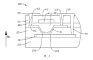
- FIG. 1 is a schematic view showing a layer structure of an array substrate of the present application
- FIG. 2 is a schematic view showing a layer structure and an opening of an array substrate of the present application
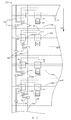
- 3 is a schematic plan view showing the principle of changing the line of the array substrate of the present application.
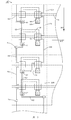
- FIG. 4 is a schematic plan view showing the principle of changing the line of another embodiment of the array substrate of the present application.
- FIG. 5 is a schematic plan view showing the principle of changing the line of another embodiment of the array substrate of the present application.
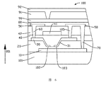
- FIG. 6 is a schematic view showing another layer structure and an opening of the array substrate of the present application.
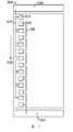
- Figure 7 is a schematic illustration of a display panel of the present application.
- the first metal layer 10 , the buffer layer 20 , the semiconductor layer 30 , the insulating layer 40 , the scanning metal layer 41 , and the internal layer are sequentially stacked on the glass substrate 101 along the first direction 001 .
- the material of the first metal layer 10 is molybdenum
- the material of the buffer layer 20 is silicon nitride and/or silicon oxide
- the semiconductor layer 30 is a low temperature poly-Si layer.
- the material of the insulating layer 40 is also silicon nitride and/or silicon oxide
- the material of the scanning metal layer 41 is molybdenum
- the material of the inner dielectric layer 42 is silicon nitride and/or silicon oxide.
- the material of the second metal layer 50 is titanium and/or aluminum.
- the first metal layer 10, the scan metal layer 41, and the second metal layer 50 are both conductive structure layers, the buffer layer 20, the inner dielectric layer 42, and the insulating layer 40. All are insulating materials
- the semiconductor layer 30 is a semiconductor material.
- the first metal layer 10 and the semiconductor layer 30, the scanning metal layer 41, and the second metal layer 50 are separated by an insulator and do not form a via. As can be seen from FIG.
- the array substrate 100 is further provided with a signal hole 60 and a via hole 70.
- the signal hole 60 is used to communicate the semiconductor layer 30 and the second metal layer 50, thereby achieving transmission of signal data to the pixel unit 200.
- the via hole 70 is used to connect the first metal layer 10 and the second metal layer 50.
- the array substrate 100 of the present application further includes a first pixel set 210 and a second pixel set 220 staggered along the second direction 002.
- the first pixel set 210 is a set of the pixel units 200 arranged along the second direction 002, and the second pixel set 220 is also a plurality of the pixels arranged along the second direction 002.
- a collection of units 200 The number of the pixel units 200 in the first pixel set 210 and the second pixel set 220 may or may not be the same. However, the first pixel set 210 and the second pixel set 220 need to be sequentially staggered along the second direction 002.
- the array substrate 100 of the present application is further provided with a first path 110 for sequentially connecting the first pixel set 210 and a second path 120 for sequentially connecting the first pixel set 210.
- a second set of pixels 220 In the first pixel set 210, the first metal layer 10 serves as a channel layer 111 of the first via 110 and a signal layer 122 of the second via, respectively, and the second metal layer 50 serves as a a signal layer 112 of the first via 110 and a channel layer 121 of the second via 120; in the second set of pixels 220, the first metal layer 10 serves as a signal layer 112 of the first via and The channel layer 121 of the second via, the second metal layer 50 serves as the channel layer 111 of the first via and the signal layer 122 of the second via, respectively.
- the channel layer 111 of the first via and the signal layer 112 of the first via are connected by a first via hole 71, and the channel layer 121 of the second via and the signal layer 122 of the second via pass The second passage holes 72 are connected.
- the signal layer 111 of the first via 110 is electrically connected to the semiconductor layer 30 through the first signal hole 61
- the signal layer 121 of the second via 120 is electrically connected to the semiconductor layer 30 through the second signal hole 62.
- the first pixel set 210 only the first signal hole 61 exists, that is, only the signal layer 112 of the first path 110 is electrically connected to the semiconductor layer 30, and the signal of the second path 120 is The layer 122 passes through the first metal layer 10 from the semiconductor layer 30 without being connected to the semiconductor layer 30.
- the first pixel set 210 only the first via 110 and the first A pixel set 210 is turned on, that is, the pixel unit 200 in the first pixel set 210 receives only signal data of the first path 110.
- the second pixel set 220 only the second signal hole 62 exists, and correspondingly, the pixel unit 200 in the second pixel set 220 receives only the signal data of the second channel 120. .
- the first path 110 and the second channel 120 sequentially communicate with the first pixel, respectively.
- the set 210 and the second set of pixels 220 that is, the first set of pixels 210 are connected in series through the first path 110, and the second set of pixels 220 are connected in series through the second path 120, two interleaved The set of pixels cross each other and not turn on, forming two separate paths.
- the first via 110 and the second via 120 are independent, so that the density of the pixel unit 200 in the unit area can be increased by the two independent driving circuits 310 respectively.
- the first via 110 and the second via 120 are connected to drive a portion of the pixels on the array substrate 100.
- the display function of the array substrate 100 can be realized together, and the resolution of the display panel can be improved.
- the array substrate 100 of the present application utilizes the first metal layer 10 and the first layer to realize the design of the first via 110 and the second via 120 separately from a prior art product.
- the wiring design of the two metal layers 50 utilizes the first metal layer 10 reasonably, eliminating the production or occupation of a metal layer, thereby eliminating a mask process, saving manufacturing costs and simplifying product structure. Reduce product thickness and improve product quality.
- the total amount of the pixel units 200 in the first pixel set 210 and the second pixel set 220 should be set equal, and each The number of the pixel units 200 in one of the first pixel sets 210 and the number of the pixel units 200 in each of the second pixel sets 220 are preferably set to be the same. This is more advantageous for the signal distribution of the two independent drive circuits 310 while maintaining the total resistance of each of the first path 110 and the second path 120, the first path 110 and the first The signal interference between the two paths 120 is more balanced, and the consistency of the real picture is guaranteed.
- a plurality of the first pixel collections 210 are sequentially arranged, and a plurality of the second pixel collections 220 are also sequentially arranged, such that the first pixel collection 210 and The second pixel collections 220 are arranged in a row on the array substrate 100 of the present application, and each of the first pixel collections 210 is arranged in a staggered manner with each of the second pixel collections 220.
- the scan metal layer 41 extends along the third direction 003 and passes through each of the first pixel collections 210 or each of the second pixel collections 220 to achieve a single row of the first pixel collections 210. Or a single row of signal conduction control of the second pixel collection 220.
- the second metal layer 50 is further used to form the pixel electrode 104 of the array substrate 100, and the pixel electrode 104 communicates with the semiconductor layer 30 through the conductive hole 105 to form A single pass of the pixel unit 200.
- the first via 110 and the second via 120 are separated by the buffer layer 20.
- the first passage hole 71 and the second passage hole 72 are also required to be separated from each other by the buffer layer 20.
- the first metal layer 10 and the second metal layer 50 need to be designed with each other in the preparation process to make the channel of the first via 110
- the passage holes 72 of the second passage 120 are spaced apart from each other.
- the semiconductor layer 30 is provided with a channel 31 for conducting between the source 102 and the drain 103 of the array substrate 100.
- the conduction of the channel 31 is achieved by the scanning metal layer 41.
- the conduction of the channel 31 is realized by a gate formed by the scanning metal layer 41 and matching the shape of the channel 31.
- signal data is transferred between the source 102 and the drain 103, and the pixel unit 200 performs a display function according to the data signal. Since the forbidden band width of the semiconductor layer 30 is narrow, an electronic transition easily occurs under illumination conditions to cause unintentional conduction of the channel 31.
- the first metal layer 10 needs to cover the channel 31 in the first direction 001.
- the first metal layer 10 also has an important function in the array substrate 100 of the present application to achieve the light shielding of the channel 31 to avoid interference of the light source under the array substrate 100 with the channel 31.
- the shape of the first metal layer 10 is set relative to the channel 31, that is, the first metal layer can effectively perform the light shielding effect as long as the channel 31 is completely covered.
- the first metal layer 10, the scanning metal layer 41, and the second metal layer 50 are in the first direction 001, in order to prevent the metal layers from blocking the light source under the array substrate 100. At least partially overlapping structures to avoid metal occlusion of light, thereby affecting the transmittance of the display panel.
- the portion of the first metal layer 10, the scanning metal layer 41, and the second metal layer 50 overlapping in the first direction 001 is larger, and the array substrate 100 is transparent. The lighter the rate.
- the width of the scanning metal layer 41 is consistent with the width of the channel 31, and the conduction function of the scanning metal layer 41 to the channel 31 can be better achieved.
- the number of the channels 31 of the semiconductor layer 30 is two.
- the two channels 31 are arranged in the third direction 003 perpendicular to the second direction 002.
- a connection line between the two channels 31 is located at an end of the channel 31 away from the signal hole 60.
- the first metal layer 10 is divided into first metal blocks 11 and second metal blocks 12 that are independent of each other.
- the first metal block 11 and the second metal block 12 are respectively used to shield the light of the two channels 31 and perform a light blocking function.
- the first metal block 11 and the second metal block 12 are also separated by the buffer layer 20 and are independent of each other.
- first via 110 and the second via 120 may be disposed to communicate with the first metal block 11 and the second metal block 12, respectively, to achieve a separate via, since the first metal block 11
- the spacing between the second metal block 12 and the second metal block 12 can effectively avoid interference between signals, and the path is realized with respect to the provision of a special patterned shape.
- This embodiment makes better use of the shape of the first metal layer 10. .
- the number of the pixel units 200 in the first pixel set 210 is 1, and the number of the pixel units 200 in the second pixel set 220 is also 1. That is, the array substrate 100 arranges the first pixel set 210 and the second pixel set 220 by means of interlaced line changing in the second direction 002.
- the first via 110 and the second via 120 respectively include a via hole 71 of the first via 110 and a via hole 72 of the second via 120 in each of the pixel units 200.
- the row-array-changing array substrate 100 takes the smallest display unit in the array substrate 100 as a line-changing design, and in the case where a certain pixel set fails and is not displayed, the pixel unit 200 can pass through the pixel unit 200
- the display compensates for the defects of a single pixel unit 200, is not easily found by the user, and the effect on the display effect is also minimized.
- the first set of pixels 210 is two of the pixel units 200.
- the second set of pixels 220 is also two of the pixel units 200 (see FIG. 5).
- the span of the first pixel set 210 and the second pixel set 220 is relatively large, the number of line changes can be reduced, that is, the number of the channel holes 70 can be reduced. This simplifies product structure and processing complexity and increases production efficiency.
- the second metal layer 50 further needs to be connected to the first pixel.
- the pixel unit 200 in the first pixel set 210 and the second pixel set 220 may also be set to two or more, so that the first path 110 and the second path 120 are each The span after the second line change is further increased. This can further reduce the number of the passage holes 70 and simplify the structure. This application is not unduly limited herein.
- a planarization layer 80 and a third metal layer 90 which are sequentially stacked in the first direction 001 are further disposed.
- the planarization layer 80 is located between the second metal layer 50 and the third metal layer 90.
- the third metal layer 90 can be disposed as a touch electrode of the array substrate 100 because there is no need for a line change.
- An insulating layer 91 made of silicon nitride is covered over the third metal layer 90, and the third metal layer 90 is connected to the upper indium tin oxide layer 92 by opening a hole in the insulating layer 91.
- the indium tin oxide layer 92 can sense a change in capacitance caused by a finger touching the liquid crystal panel, thereby implementing a touch control function.
- the array substrate 100 described in the present application achieves the effect of disposing the third metal layer 90 as a touch sensing line because the third metal layer 90 disposed as a line change is saved. Further, the arrangement of the third metal layer 90 on the array substrate 100 can compress the thickness of the array substrate 100 to realize the function of the In Cell Touch.
- the present application also relates to a display panel 300 (see FIG. 7).
- the display panel 300 may be a liquid crystal panel or an OLED panel.
- the type of the display panel 300 is not limited thereto.
- the display panel 300 includes the array substrate 100 described above, and the drive circuit 310 that is disposed at two ends of the array substrate 100 along the second direction 002.
- One of the driving circuits 310 is electrically connected to the first via 110, and the other of the driving circuits 310 is electrically connected to the second via 120.
- the display panel 300 is driven by two independent driving circuits 310 to respectively drive two groups on the array substrate 100.
- the pixel unit 200 reduces the load of a single of the driving circuit 310, and effectively avoids delay defects of signals.
- the mobile terminal according to the present application has higher screen resolution and a thinner body because the display panel 300 is included, and the overall quality is improved.
Landscapes
- Devices For Indicating Variable Information By Combining Individual Elements (AREA)
- Mechanical Light Control Or Optical Switches (AREA)
- Liquid Crystal (AREA)
Abstract
本申请涉及显示面板领域,一种阵列基板,包括沿第一方向依次层叠于玻璃基板上的第一金属层、缓冲层、半导体层、绝缘层、扫描金属层、内介电层和第二金属层,还包括沿第二方向交错排列的第一像素集合和第二像素集合,以及依次连通所述第一像素集合的第一通路和依次连通所述第二像素集合和第二通路。所述第一通路和所述第二通路在所述第一层金属层和所述第二层金属层中交叉换线,从而分别依次串联所述第一像素集合和所述第二像素集合。本申请阵列基板,可省去专门的换线金属层,降低制程成本,同时实现In Cell Touch功能,提升产品性能和品质附加值。
Description
本申请涉及显示面板领域,尤其涉及一种阵列基板,以及包含此阵列基板的显示面板和移动终端。
在显示领域,一般通过增加单位面积像素密度的方法提高显示面板的分辨率。在这种结构中,像素密度增加,导致驱动电路(IC-integrated circuit)负载过大,信号传输延迟,易造成显示不良,产品可靠性下降。当前行业内的解决方案是采用显示面板顶部和底部两个驱动电路同时输入信号,在原信号线金属层的基础上再叠加一层金属层,通过双层金属换线的方式来实现每个驱动电路特定驱动一部分像素,避免单个驱动电路负载过大导致的信号延迟。这种方案的缺点在于,换线金属的制作需要新增一道光罩,增加了成本和制程,降低产能;且叠加的金属层作为换线的信号线存在,则不能用作触控电极。由此触控功能只能叠加在换线的信号线之上(即On Cell Touch方式,也称作Add on方式)予以实现,导致整机厚度和质量增加,产品定位局限中低端市场。
发明内容
本申请本提出应用于高分辨率显示面板信号线走线的一种阵列基板,可省去换线金属光罩,降低制程成本,同时实现In Cell Touch功能,提升产品性能和品质附加值。本申请包括如下技术方案:
一种阵列基板,包括沿第一方向依次层叠于玻璃基板上的第一金属层、缓 冲层、半导体层、绝缘层、扫描金属层、内介电层和第二金属层,以及连通所述半导体层和所述第二金属层的信号孔,和连通所述第一金属层和所述第二金属层的通道孔;所述阵列基板还包括沿第二方向交错排列的第一像素集合和第二像素集合;以及依次连通所述第一像素集合的第一通路和依次连通所述第二像素集合和第二通路;在所述第一像素集合中,所述第一金属层分别作为所述第一通路的通道层和所述第二通路的信号层,所述第二金属层分别作为所述第一通路的信号层和所述第二通路的通道层;在所述第二像素集合中,所述第一金属层分别作为所述第一通路的信号层和所述第二通路的通道层,所述第二金属层分别作为所述第一通路的通道层和所述第二通路的信号层。
其中,所述第一像素集合中像素单元的数量和所述第二像素集合中所述像素单元的数量相同。
其中,所述第一金属层和所述第二金属层相互配合有图案化线路,以使得所述第一通路的通道孔和所述第二通路的通道孔相互隔开。
其中,所述半导体层设有用于所述阵列基板的源极和漏极之间导通的沟道,所述第一金属层在所述第一方向上覆盖所述沟道以实现所述沟道的遮光。
其中,在单个像素单元中,所述半导体层的所述沟道为两个,两个所述沟道沿垂直于所述第二方向的第三方向排列,所述第一金属层分为相互独立的第一金属块和第二金属块,所述第一金属块和所述第二金属块分别用于遮挡两个所述沟道的光线,所述第一通路和所述第二通路分别连通所述第一金属块和所述第二金属块。
其中,所述第一像素集合只包含一个像素单元,所述第二像素集合也只包含一个像素单元,每一个所述像素单元中均包含所述第一通路的通道孔和所述 第二通路的通道孔。
其中,所述第一像素集合为至少两个像素单元,所述第二像素集合也为至少两个像素单元,所述第一像素集合与所述第二像素集合中的所述第二金属层还包括依次连通所述第一像素集合或所述第二像素集合中所述像素单元的信号线,以及依次连通所述第一金属层的通道线。
其中,所述阵列基板还包括沿所述第一方向依次层叠的平坦化层和第三金属层,所述平坦化层位于所述第二金属层和所述第三金属层之间。
其中,所述阵列基板还包括沿所述第一方向依次层叠的平坦化层和第三金属层,所述平坦化层位于所述第二金属层和所述第三金属层之间。
其中,所述阵列基板还包括沿所述第一方向依次层叠的平坦化层和第三金属层,所述平坦化层位于所述第二金属层和所述第三金属层之间。
其中,所述阵列基板还包括沿所述第一方向依次层叠的平坦化层和第三金属层,所述平坦化层位于所述第二金属层和所述第三金属层之间。
其中,所述阵列基板还包括沿所述第一方向依次层叠的平坦化层和第三金属层,所述平坦化层位于所述第二金属层和所述第三金属层之间。
其中,所述阵列基板还包括沿所述第一方向依次层叠的平坦化层和第三金属层,所述平坦化层位于所述第二金属层和所述第三金属层之间。
其中,所述阵列基板还包括沿所述第一方向依次层叠的平坦化层和第三金属层,所述平坦化层位于所述第二金属层和所述第三金属层之间。
本申请还涉及一种显示面板,包括上述阵列基板,以及沿所述第二方向分列所述阵列基板两端的第一驱动电路和第二驱动电路,所述第一驱动电路与所述第一通路电连接,所述第二驱动电路与所述第二通路电连接。
本申请涉及一种移动终端,包含上述显示面板。
本申请所述阵列基板,通过沿第一方向依次层叠于所述玻璃基板上的所述第一金属层、所述缓冲层、所述半导体层、所述绝缘层和所述第二金属层,实现了所述第一金属层、所述半导体层和所述第二金属层相互绝缘隔离的作用。通过所述信号孔和所述通道孔的设置,将所述第一金属层和所述半导体层分别与所述第二金属层连通,从而实现了换线和信号导通的基础。通过第一像素集合第二像素集的设置,将所述阵列基板内的像素进行二分,减小了驱动电路的压力。通过所述第一通路和所述第二通道在所述第一像素集和所述第二像素集中的换线,将所述第一像素集和所述第二像素集分别依次连接,从而实现了本申请所述阵列基板分别驱动的功能。本申请所述阵列基板,利用原有的所述第一金属层作为换线功能的导线,省去了单独设置第三金属层进行换线的必要。因此,本申请所述阵列基板,相比于现有技术而言简化了结构,省去了一道光罩制程,简化工艺节约成本,同时还实现了基板的薄型化,提高产品品质。
图1是本申请阵列基板的层结构示意图;
图2是本申请阵列基板的层结构及开孔示意图;
图3是本申请阵列基板换线原理的平面示意图;
图4是本申请阵列基板另一实施例换线原理的平面示意图;
图5是本申请阵列基板再一实施例换线原理的平面示意图;
图6是本申请阵列基板另一层结构及开孔的示意图;
图7是本申请显示面板的示意图。
下面将结合本申请实施例中的附图,对本申请实施例中的技术方案进行清楚、完整地描述,显然,所描述的实施例仅仅是本申请的一部分实施例,而不是全部的实施例。基于本申请中的实施例,本领域普通技术人员在没有做出创造性劳动的前提下所获得的所有其它实施例,都属于本申请保护的范围。
请参阅图1所示的阵列基板100,包括沿第一方向001依次层叠于玻璃基板101上的第一金属层10、缓冲层20、半导体层30、绝缘层40、扫描金属层41、内介电层42和第二金属层50。依次的,所述第一金属层10的材料为钼,所述缓冲层20的材料为氮化硅和/或氧化硅,所述半导体层30为低温多晶硅(low temperature Poly-Si)层,所述绝缘层40的材料也为氮化硅和/或氧化硅,所述扫描金属层41的材料为钼,所述内介电层42的材料为氮化硅和/或氧化硅,所述第二金属层50的材料为钛和/或铝。由此,所述第一金属层10、所述扫描金属层41和所述第二金属层50均为导电结构层,所述缓冲层20、所述内介电层42和所述绝缘层40均为绝缘材料,所述半导体层30为半导体材料。所述第一金属层10与所述半导体层30、所述扫描金属层41以及所述第二金属层50之间均通过绝缘体隔开,彼此不形成通路。通过图2可以看出,所述阵列基板100还设有信号孔60和通道孔70。所述信号孔60用于连通所述半导体层30和所述第二金属层50,从而实现信号数据向像素单元200的传输。所述通道孔70用于连通所述第一金属层10和所述第二金属层50。
见图3,本申请所述阵列基板100还包括沿第二方向002交错排列的第一像素集合210和第二像素集合220。所述第一像素集合210为若干个沿所述第 二方向002排列的所述像素单元200的集合,所述第二像素集合220也为若干个沿所述第二方向002排列的所述像素单元200的集合。所述第一像素集合210和所述第二像素集合220中所述像素单元200的数量可以一致,也可以不一致。但所述第一像素集合210与所述第二像素集合220需要沿所述第二方向002依次交错设置。本申请所述阵列基板100还设有第一通路110和第二通路120,所述第一通路110用于依次连通所述第一像素集合210,所述第二通路220用于依次连通所述第二像素集合220。在所述第一像素集合210中,所述第一金属层10分别作为所述第一通路110的通道层111和所述第二通路的信号层122,所述第二金属层50分别作为所述第一通路110的信号层112和所述第二通路120的通道层121;在所述第二像素集合中220,所述第一金属层10分别作为所述第一通路的信号层112和所述第二通路的通道层121,所述第二金属层50分别作为所述第一通路的通道层111和所述第二通路的信号层122。所述第一通路的通道层111和所述第一通路的信号层112之间通过第一通道孔71连接,所述第二通路的通道层121和所述第二通路的信号层122也通过第二通道孔72连接。所述第一通路110的信号层111通过第一信号孔61与所述半导体层30导通,所述第二通路120的信号层121通过第二信号孔62与所述半导体层30导通。由于所述第一像素集合210中,只有所述第一信号孔61存在,即只有所述第一通路110的信号层112与所述半导体层30导通,而所述第二通路120的信号层122通过所述第一金属层10通过从所述半导体层30而不与所述半导体层30发生连接,因此在所述第一像素集合210中,只有所述第一通路110与所述第一像素集合210导通,即所述第一像素集合210中的所述像素单元200只接收所述第一通路110的信号数据。而在所述第二像 素集合220中,只有所述第二信号孔62存在,则相应的,所述第二像素集合220中的所述像素单元200只接收所述第二通道120的信号数据。在所述第一像素集合210和所述第二像素集合220沿所述第二方向002交错设置的过程中,所述第一通路110和所述第二通道120分别依次连通所述第一像素集合210和所述第二像素集合220,也即所述第一像素集合210通过所述第一通路110串联,所述第二像素集合220通过所述第二通路120串联,两个交错设置的像素集合彼此交叉而不导通,形成了两个独立的通路。
所述第一通路110与所述第二通路120的独立,使得在本申请所述阵列基板100在单位面积内所述像素单元200密度提升的基础上,可以通过两个独立的驱动电路310分别连接所述第一通路110和所述第二通路120来驱动所述阵列基板100上的一部分像素。当两个独立的所述驱动电路310信号相互配合时,可以共同实现所述阵列基板100的显示功能,提高显示面板的分辨率。而相对于现有产品中单独设置一层金属层来实现所述第一通路110和所述第二通路120的设计,本申请所述阵列基板100利用所述第一金属层10和所述第二金属层50的换线设计合理利用了所述第一金属层10,省去了一道金属层的制作或占用,由此省去了一道光罩制程,节约了制造成本,同时简化了产品结构,降低产品厚度,提升了产品品质。
可以理解的,为了平衡两个独立的所述驱动电路310的功率,所述第一像素集合210和所述第二像素集合220内的所述像素单元200的总量宜设置为相等,且每一个所述第一像素集合210中的所述像素单元200数量与每一个所述第二像素集合220中的所述像素单元200的数量宜设置为相同。这样更有利于两个独立的所述驱动电路310的信号分配,同时使得所述第一通路110和所述 第二通路120各自的总电阻保持不变,所述第一通路110和所述第二通路120之间的信号干扰更均衡,现实画面的一致性得以保证。
在垂直于所述第二方向002的第三方向003上,多个所述第一像素合集210依次排列,多个所述第二像素合集220也依次排列,使得所述第一像素合集210和所述第二像素合集220均成排布置于本申请所述阵列基板100上,且每一排所述第一像素合集210与每一排所述第二像素合集220交错设置。扫描金属层41沿所述第三方向003延伸,并穿过每一排所述第一像素合集210或每一排所述第二像素合集220,以实现对单排所述第一像素合集210或单排所述第二像素合集220的信号导通控制。
进一步的,见图2和图3,所述第二金属层50还用于形成所述阵列基板100的像素电极104,所述像素电极104通过导电孔105与所述半导体层30连通,以形成单个所述像素单元200的通路。
在所述第一像素集合210和所述第二像素集合220的内部,所述第一通路110与所述第二通路120通过所述缓冲层20被分隔开。为了保持所述第一通路110与所述第二通路120之间也隔离开,需要所述第一通道孔71和所述第二通道孔72也彼此通过所述缓冲层20分隔开。由此,一种实施例,所述第一金属层10和所述第二金属层50在各自的制备过程中,需要设计相互配合的图案化线路,以使得所述第一通路110的通道孔71和所述第二通路120的通道孔72相互隔开。
在本申请所述阵列基板100中,所述半导体层30设有用于所述阵列基板100的源极102和漏极103之间导通的沟道31。所述第一通路110和所述第二通路120的信号数据通过所述信号孔60传入所述半导体层30后,通过所述扫 描金属层41来实现所述沟道31的导通。具体的,通过所述扫描金属层41形成的与所述沟道31形状匹配的栅极来实现所述沟道31的导通。从而实现信号数据在所述源极102和所述漏极103之间的传递,进而所述像素单元200根据数据信号施行显示功能。由于所述半导体层30的禁带宽度较窄,在光照条件下容易发生电子跃迁而导致所述沟道31的非故意导通。为此,所述第一金属层10在所述第一方向001上需要覆盖所述沟道31。所述第一金属层10在本申请所述阵列基板100中还有一个重要的作用即实现所述沟道31的遮光,避免所述阵列基板100下方的光源对所述沟道31的干扰。
可以理解的,所述第一金属层10的形状相对于所述沟道31来设定,即所述第一金属层只要完全覆盖所述沟道31就可以有效实施遮光作用。而为了避免各金属层对所述阵列基板100下方的光源的遮挡,所述第一金属层10、所述扫描金属层41、和所述第二金属层50在所述第一方向001上呈至少部分重叠的结构,以避免金属对光的遮挡,进而影响显示面板透光率。在这些实施例中,所述第一金属层10、所述扫描金属层41、和所述第二金属层50在所述第一方向001上重叠的部分越大,所述阵列基板100的透光率越强。
另一方面,一些实施例中,所述扫描金属层41的宽度与所述沟道31的宽度一致,可以更好的实现所述扫描金属层41对所述沟道31的导通功能。
在图4的实施例中,在单个所述像素单元200中,所述半导体层30的所述沟道31为两个。两个所述沟道31沿垂直于所述第二方向002的所述第三方向003排列。两个所述沟道31之间的连接线位于所述沟道31远离所述信号孔60的一端。相应的,在单个所述像素单元200中,所述第一金属层10分为相互独立的第一金属块11和第二金属块12。所述第一金属块11和所述第二金 属块12分别用于遮挡两个所述沟道31的光线,施行遮光功能。所述第一金属块11与所述第二金属块12也被所述缓冲层20所分隔而相互独立。由此,所述第一通路110和所述第二通路120可设置为分别连通所述第一金属块11和所述第二金属块12来实现分隔的通路,由于所述第一金属块11和所述第二金属块12之间的间隔设置可以有效避免信号间的干扰,相对于设置专门的图形化形状来实现通路,本实施例更好的利用了所述第一金属层10的形状。
在图3和图4的实施例中,所述第一像素集合210中的所述像素单元200数量为1,所述第二像素集合220中所述像素单元200的数量也为1。即所述阵列基板100在所述第二方向002上采用隔行换线的方式来布置所述第一像素集合210和所述第二像素集合220。所述第一通路110和所述第二通路120在每一个所述像素单元200中均同时包含所述第一通路110的通道孔71和所述第二通路120的通道孔72。逐行换线的所述阵列基板100取所述阵列基板100中的最小显示单元做换线设计,在某一像素集合出现故障而不显示的情况下,可以通过其周围的所述像素单元200的显示来弥补单个所述像素单元200的缺陷,不易被用户发现,对显示效果的影响也得以降到最低限度。
在另一种实施方式中,所述第一像素集合210为两个所述像素单元200。相应的,所述第二像素集合220也为两个所述像素单元200(见图5)。当所述第一像素集合210和所述第二像素集合220的跨度比较大时,可以减少换线的数量,即减少所述通道孔70的数量。这样可以简化产品结构和加工复杂性,提升生产效率。可以理解的,为了实现所述第一像素集合210与所述第二像素集合220中各个所述像素单元200的信号依次导通,所述第二金属层50还需要设置连通所述第一像素集合210或所述第二像素集合220中所述像素单元 200的信号线63。同样的,在所述第一金属层10中,也需要设置依次连通每个所述像素单元200中的所述第一金属层10的通过线73。
可以理解的,所述第一像素集合210和所述第二像素集合220中的所述像素单元200还可以均设置为两个以上,让所述第一通路110和所述第二通路120每次换线后的跨度进一步增大。这样可以进一步减少所述通道孔70的数量,简化结构。本申请在此不做过度限定。
一种实施例,见图6,在上述阵列基板100的基础上,还设置了沿所述第一方向001依次层叠的平坦化层80和第三金属层90。其中所述平坦化层80位于所述第二金属层50和所述第三金属层90之间。所述第三金属层90因为没有了换线的需求,可以被设置为所述阵列基板100的触控电极。在所述第三金属层90的上方覆盖材料为氮化硅的绝缘层91,通过在所述绝缘层91上开孔,使得所述第三金属层90与上层的氧化铟锡层92相连。所述氧化铟锡层92可以感应手指触摸液晶屏引起的电容变化,因而实现触摸控制功能。本申请所述阵列基板100正是因为节约了作为换线设置的所述第三金属层90,才得以实现将所述第三金属层90设置为触摸感应线的效果。进一步的,所述第三金属层90在所述阵列基板100上的设置,得以压缩所述阵列基板100的厚度,实现In Cell Touch的功能。
本申请还涉及一种显示面板300(见图7),所述显示面板300可以是液晶面板,也可以使OLED面板,所述显示面板300的种类不限于此。所述显示面板300包括上述阵列基板100,以及沿所述第二方向002分列所述阵列基板100两端的所述驱动电路310。其中一个所述驱动电路310与所述第一通路110电连接,另一个所述驱动电路310与所述第二通路120电连接。由此即利用本 申请所述阵列基板100上两条独立信号通道的结构设置,实现了所述显示面板300通过两个独立的所述驱动电路310以分别驱动所述阵列基板100上的两组所述像素单元200,降低了单个所述驱动电路310的负载,有效避免信号的延迟缺陷。
可以理解的,本申请所涉及的移动终端,因为包含了所述显示面板300,而具备了更高的屏幕清晰度,更薄的机身,整体品质得以提升。
以上所述的实施方式,并不构成对该技术方案保护范围的限定。任何在上述实施方式的精神和原则之内所作的修改、等同替换和改进等,均应包含在该技术方案的保护范围之内。
Claims (16)
- 一种阵列基板,其中,包括沿第一方向依次层叠于玻璃基板上的第一金属层、缓冲层、半导体层、绝缘层、扫描金属层、内介电层和第二金属层,以及连通所述半导体层和所述第二金属层的信号孔,和连通所述第一金属层和所述第二金属层的通道孔;所述阵列基板还包括沿第二方向交错排列的第一像素集合和第二像素集合;以及依次连通所述第一像素集合的第一通路和依次连通所述第二像素集合和第二通路;在所述第一像素集合中,所述第一金属层分别作为所述第一通路的通道层和所述第二通路的信号层,所述第二金属层分别作为所述第一通路的信号层和所述第二通路的通道层;在所述第二像素集合中,所述第一金属层分别作为所述第一通路的信号层和所述第二通路的通道层,所述第二金属层分别作为所述第一通路的通道层和所述第二通路的信号层。
- 如权利要求1所述阵列基板,其中,所述第一像素集合中像素单元的数量和所述第二像素集合中所述像素单元的数量相同。
- 如权利要求2所述阵列基板,其中,所述第一金属层和所述第二金属层相互配合有图案化线路,以使得所述第一通路的通道孔和所述第二通路的通道孔相互隔开。
- 如权利要求3所述阵列基板,其中,所述半导体层设有用于所述阵列基板的源极和漏极之间导通的沟道,所述第一金属层在所述第一方向上覆盖所述沟道以实现所述沟道的遮光。
- 如权利要求4所述阵列基板,其中,在单个像素单元中,所述半导体层的所述沟道为两个,两个所述沟道沿垂直于所述第二方向的第三方向排列,所述第一金属层分为相互独立的第一金属块和第二金属块,所述第一金属块和所述第二金属块分别用于遮挡两个所述沟道的光线,所述第一通路和所述第二通路分别连通所述第一金属块和所述第二金属块。
- 如权利要求1所述阵列基板,其中,所述第一像素集合只包含一个像素单元,所述第二像素集合也只包含一个像素单元,每一个所述像素单元中均包含所述第一通路的通道孔和所述第二通路的通道孔。
- 如权利要求1所述阵列基板,其中,所述第一像素集合为至少两个像素单元,所述第二像素集合也为至少两个像素单元,所述第一像素集合与所述第二像素集合中的所述第二金属层还包括依次连通所述第一像素集合或所述第二像素集合中所述像素单元的信号线,以及依次连通所述第一金属层的通道线。
- 如权利要求1所述阵列基板,其中,所述阵列基板还包括沿所述第一方向依次层叠的平坦化层和第三金属层,所述平坦化层位于所述第二金属层和 所述第三金属层之间。
- 如权利要求2所述阵列基板,其中,所述阵列基板还包括沿所述第一方向依次层叠的平坦化层和第三金属层,所述平坦化层位于所述第二金属层和所述第三金属层之间。
- 如权利要求3所述阵列基板,其中,所述阵列基板还包括沿所述第一方向依次层叠的平坦化层和第三金属层,所述平坦化层位于所述第二金属层和所述第三金属层之间。
- 如权利要求4所述阵列基板,其中,所述阵列基板还包括沿所述第一方向依次层叠的平坦化层和第三金属层,所述平坦化层位于所述第二金属层和所述第三金属层之间。
- 如权利要求5所述阵列基板,其中,所述阵列基板还包括沿所述第一方向依次层叠的平坦化层和第三金属层,所述平坦化层位于所述第二金属层和所述第三金属层之间。
- 如权利要求6所述阵列基板,其中,所述阵列基板还包括沿所述第一方向依次层叠的平坦化层和第三金属层,所述平坦化层位于所述第二金属层和所述第三金属层之间。
- 如权利要求7所述阵列基板,其中,所述阵列基板还包括沿所述第一方向依次层叠的平坦化层和第三金属层,所述平坦化层位于所述第二金属层和所述第三金属层之间。
- 一种显示面板,其中,包括权利要求1所述阵列基板,以及沿所述第二方向分列所述阵列基板两端的第一驱动电路和第二驱动电路,所述第一驱动电路与所述第一通路电连接,所述第二驱动电路与所述第二通路电连接。
- 一种移动终端,其中,所述移动终端包含权利要求15所述显示面板。
Priority Applications (1)
| Application Number | Priority Date | Filing Date | Title |
|---|---|---|---|
| US16/110,197 US10551705B2 (en) | 2018-02-28 | 2018-08-23 | Array substrate, display panel and mobile terminal |
Applications Claiming Priority (2)
| Application Number | Priority Date | Filing Date | Title |
|---|---|---|---|
| CN201810168022.7 | 2018-02-28 | ||
| CN201810168022.7A CN108364931B (zh) | 2018-02-28 | 2018-02-28 | 阵列基板、显示面板和移动终端 |
Related Child Applications (1)
| Application Number | Title | Priority Date | Filing Date |
|---|---|---|---|
| US16/110,197 Continuation US10551705B2 (en) | 2018-02-28 | 2018-08-23 | Array substrate, display panel and mobile terminal |
Publications (1)
| Publication Number | Publication Date |
|---|---|
| WO2019165682A1 true WO2019165682A1 (zh) | 2019-09-06 |
Family
ID=63002845
Family Applications (1)
| Application Number | Title | Priority Date | Filing Date |
|---|---|---|---|
| PCT/CN2018/082640 Ceased WO2019165682A1 (zh) | 2018-02-28 | 2018-04-11 | 阵列基板、显示面板和移动终端 |
Country Status (2)
| Country | Link |
|---|---|
| CN (1) | CN108364931B (zh) |
| WO (1) | WO2019165682A1 (zh) |
Citations (3)
| Publication number | Priority date | Publication date | Assignee | Title |
|---|---|---|---|---|
| US6229506B1 (en) * | 1997-04-23 | 2001-05-08 | Sarnoff Corporation | Active matrix light emitting diode pixel structure and concomitant method |
| CN104022127A (zh) * | 2014-05-30 | 2014-09-03 | 京东方科技集团股份有限公司 | 一种阵列基板及其制作方法、以及显示装置 |
| CN107272290A (zh) * | 2017-07-18 | 2017-10-20 | 深圳市华星光电技术有限公司 | 一种阵列基板以及显示面板 |
Family Cites Families (2)
| Publication number | Priority date | Publication date | Assignee | Title |
|---|---|---|---|---|
| KR101776044B1 (ko) * | 2010-11-02 | 2017-09-20 | 엘지디스플레이 주식회사 | 유기전계 발광소자용 기판 및 그 제조 방법 |
| KR102185102B1 (ko) * | 2014-01-10 | 2020-12-02 | 삼성디스플레이 주식회사 | 어레이 기판, 이를 갖는 액정 표시 패널 및 이의 제조방법 |
-
2018
- 2018-02-28 CN CN201810168022.7A patent/CN108364931B/zh active Active
- 2018-04-11 WO PCT/CN2018/082640 patent/WO2019165682A1/zh not_active Ceased
Patent Citations (3)
| Publication number | Priority date | Publication date | Assignee | Title |
|---|---|---|---|---|
| US6229506B1 (en) * | 1997-04-23 | 2001-05-08 | Sarnoff Corporation | Active matrix light emitting diode pixel structure and concomitant method |
| CN104022127A (zh) * | 2014-05-30 | 2014-09-03 | 京东方科技集团股份有限公司 | 一种阵列基板及其制作方法、以及显示装置 |
| CN107272290A (zh) * | 2017-07-18 | 2017-10-20 | 深圳市华星光电技术有限公司 | 一种阵列基板以及显示面板 |
Also Published As
| Publication number | Publication date |
|---|---|
| CN108364931A (zh) | 2018-08-03 |
| CN108364931B (zh) | 2020-01-03 |
Similar Documents
| Publication | Publication Date | Title |
|---|---|---|
| CN111180494B (zh) | 一种显示面板及显示装置 | |
| US10970513B2 (en) | Array substrate, display screen, and electronic device | |
| JP7052966B2 (ja) | タッチ制御表示パネル | |
| US11199750B2 (en) | Display panel having black matrix comprising extension portions | |
| US10338724B2 (en) | Array substrate and method for fabricating the same, and display device and method for driving the same | |
| CN107340921B (zh) | 触控面板 | |
| CN108717245B (zh) | 显示面板和显示装置 | |
| CN108445686A (zh) | 阵列基板、显示面板与显示装置 | |
| CN116610231A (zh) | 触控显示面板及触控显示装置 | |
| CN107506076B (zh) | 一种触控显示基板、制造方法及显示装置 | |
| CN111625119B (zh) | 触摸屏及显示装置 | |
| WO2016106808A1 (zh) | 触控显示装置及电子设备 | |
| CN111708237B (zh) | 一种阵列基板、显示面板及显示装置 | |
| CN107678590A (zh) | 一种触控显示面板及其驱动方法 | |
| WO2020088279A1 (zh) | 显示基板及显示装置 | |
| JP7358240B2 (ja) | デマルチプレクサ、それを備えたアレイ基板、及び表示装置 | |
| CN109062441B (zh) | 阵列基板 | |
| US20260056635A1 (en) | Touch display substrate, manufacturing method thereof and touch display apparatus | |
| CN114975570B (zh) | 显示面板和显示装置 | |
| CN115311975B (zh) | 一种显示面板及显示装置 | |
| CN113540124B (zh) | 一种阵列基板、显示面板及显示装置 | |
| CN115268132A (zh) | 显示装置及其显示面板 | |
| US10551705B2 (en) | Array substrate, display panel and mobile terminal | |
| US20240215383A1 (en) | Display panel and electronic device | |
| WO2019165682A1 (zh) | 阵列基板、显示面板和移动终端 |
Legal Events
| Date | Code | Title | Description |
|---|---|---|---|
| 121 | Ep: the epo has been informed by wipo that ep was designated in this application |
Ref document number: 18908045 Country of ref document: EP Kind code of ref document: A1 |
|
| NENP | Non-entry into the national phase |
Ref country code: DE |
|
| 122 | Ep: pct application non-entry in european phase |
Ref document number: 18908045 Country of ref document: EP Kind code of ref document: A1 |