WO2019163376A1 - Module d'antenne et dispositif de communication disposant du module d'antenne en son sein - Google Patents
Module d'antenne et dispositif de communication disposant du module d'antenne en son sein Download PDFInfo
- Publication number
- WO2019163376A1 WO2019163376A1 PCT/JP2019/002029 JP2019002029W WO2019163376A1 WO 2019163376 A1 WO2019163376 A1 WO 2019163376A1 JP 2019002029 W JP2019002029 W JP 2019002029W WO 2019163376 A1 WO2019163376 A1 WO 2019163376A1
- Authority
- WO
- WIPO (PCT)
- Prior art keywords
- dielectric layer
- antenna module
- radiating element
- antenna
- disposed
- Prior art date
Links
Images


Classifications
-
- H—ELECTRICITY
- H01—ELECTRIC ELEMENTS
- H01Q—ANTENNAS, i.e. RADIO AERIALS
- H01Q1/00—Details of, or arrangements associated with, antennas
- H01Q1/12—Supports; Mounting means
- H01Q1/22—Supports; Mounting means by structural association with other equipment or articles
- H01Q1/2208—Supports; Mounting means by structural association with other equipment or articles associated with components used in interrogation type services, i.e. in systems for information exchange between an interrogator/reader and a tag/transponder, e.g. in Radio Frequency Identification [RFID] systems
-
- H—ELECTRICITY
- H01—ELECTRIC ELEMENTS
- H01Q—ANTENNAS, i.e. RADIO AERIALS
- H01Q1/00—Details of, or arrangements associated with, antennas
- H01Q1/12—Supports; Mounting means
- H01Q1/22—Supports; Mounting means by structural association with other equipment or articles
- H01Q1/2283—Supports; Mounting means by structural association with other equipment or articles mounted in or on the surface of a semiconductor substrate as a chip-type antenna or integrated with other components into an IC package
-
- H—ELECTRICITY
- H01—ELECTRIC ELEMENTS
- H01Q—ANTENNAS, i.e. RADIO AERIALS
- H01Q1/00—Details of, or arrangements associated with, antennas
- H01Q1/36—Structural form of radiating elements, e.g. cone, spiral, umbrella; Particular materials used therewith
- H01Q1/38—Structural form of radiating elements, e.g. cone, spiral, umbrella; Particular materials used therewith formed by a conductive layer on an insulating support
-
- H—ELECTRICITY
- H01—ELECTRIC ELEMENTS
- H01Q—ANTENNAS, i.e. RADIO AERIALS
- H01Q1/00—Details of, or arrangements associated with, antennas
- H01Q1/50—Structural association of antennas with earthing switches, lead-in devices or lightning protectors
-
- H—ELECTRICITY
- H01—ELECTRIC ELEMENTS
- H01Q—ANTENNAS, i.e. RADIO AERIALS
- H01Q21/00—Antenna arrays or systems
- H01Q21/0006—Particular feeding systems
- H01Q21/0075—Stripline fed arrays
-
- H—ELECTRICITY
- H01—ELECTRIC ELEMENTS
- H01Q—ANTENNAS, i.e. RADIO AERIALS
- H01Q21/00—Antenna arrays or systems
- H01Q21/06—Arrays of individually energised antenna units similarly polarised and spaced apart
- H01Q21/08—Arrays of individually energised antenna units similarly polarised and spaced apart the units being spaced along or adjacent to a rectilinear path
-
- H—ELECTRICITY
- H01—ELECTRIC ELEMENTS
- H01Q—ANTENNAS, i.e. RADIO AERIALS
- H01Q5/00—Arrangements for simultaneous operation of antennas on two or more different wavebands, e.g. dual-band or multi-band arrangements
- H01Q5/30—Arrangements for providing operation on different wavebands
- H01Q5/307—Individual or coupled radiating elements, each element being fed in an unspecified way
- H01Q5/342—Individual or coupled radiating elements, each element being fed in an unspecified way for different propagation modes
- H01Q5/357—Individual or coupled radiating elements, each element being fed in an unspecified way for different propagation modes using a single feed point
-
- H—ELECTRICITY
- H01—ELECTRIC ELEMENTS
- H01Q—ANTENNAS, i.e. RADIO AERIALS
- H01Q9/00—Electrically-short antennas having dimensions not more than twice the operating wavelength and consisting of conductive active radiating elements
- H01Q9/04—Resonant antennas
- H01Q9/0407—Substantially flat resonant element parallel to ground plane, e.g. patch antenna
Definitions
- the present disclosure relates to an antenna module and a communication device including the antenna module, and more particularly to an antenna structure capable of reducing an effective dielectric constant.
- Patent Document 1 discloses an antenna module in which an antenna element and a high-frequency semiconductor element are integrally mounted on a dielectric substrate.
- antenna characteristics such as frequency bandwidth, peak gain, and loss of a transmittable high-frequency signal are affected by the dielectric constant of the dielectric substrate on which the antenna element is mounted.
- the lower the relative dielectric constant ( ⁇ r) and the dielectric loss tangent (tan ⁇ ) of the dielectric substrate the better. Therefore, in order to realize a high peak gain of the antenna and reduce the power consumption of the device, it is necessary to reduce the dielectric constant of the dielectric substrate.
- the frequency bandwidth generally, the thicker the thickness of the dielectric substrate (that is, the distance between the antenna element and the ground electrode), the wider the frequency bandwidth.
- the dielectric substrate is reduced in thickness, the frequency bandwidth of the antenna becomes narrower. Can cause problems.
- the present disclosure has been made to solve such a problem, and an object thereof is to realize a wide band and a low loss in the antenna module.
- the antenna module according to the present disclosure includes at least one radiating element, a ground electrode, and a dielectric layer provided between the at least one radiating element and the ground electrode, on which the at least one radiating element is mounted.
- a space is formed between the dielectric layer and the ground electrode in a region where at least one radiating element and the ground electrode overlap when the dielectric layer is viewed in plan.
- the dielectric layer has a first part in which at least one radiating element is arranged and a second part in which at least one radiating element is not arranged.
- the thickness of the dielectric layer in the normal direction in the second portion is smaller than the thickness of the dielectric layer in the normal direction in the first portion.
- the antenna module further includes at least one feeder circuit and a feeder line.
- At least one power supply circuit is mounted on the dielectric layer and configured to supply high frequency power to the at least one radiating element.
- the feeder line is formed in the dielectric layer, and transmits high-frequency power from at least one feeder circuit to at least one radiating element.
- the antenna module further includes at least one power feeding circuit mounted on the dielectric layer and configured to supply high frequency power to at least one radiating element.
- At least one feeder circuit is disposed in the first portion of the dielectric layer.
- the antenna module further includes at least one power feeding circuit mounted on the dielectric layer and configured to supply high frequency power to at least one radiating element.
- At least one feeder circuit is disposed in the second portion of the dielectric layer.
- the antenna module further includes at least one power feeding circuit mounted on the dielectric layer and configured to supply high frequency power to at least one radiating element.
- the dielectric layer further includes a third portion that is thicker in the normal direction than the second portion and that is different from the first portion. At least one power supply circuit is arranged in the third part.
- the antenna module further includes another radiating element arranged in the third portion.
- the at least one feeding circuit is disposed on a surface opposite to the surface on which the other radiating elements are disposed in the third portion.
- At least one radiating element there are a plurality of at least one radiating element, and they are arranged apart from each other in the plane direction of the dielectric layer.
- a feeding circuit is provided corresponding to each radiating element.
- the upper surface of the second portion is continuous with the lower surface of the space formed in the dielectric layer.
- the ground electrode is formed on the lower surface of the space.
- the entire at least one radiating element overlaps the space.
- the dielectric layer has a first portion where one end portion of the dielectric layer is bent and opposed, and a second portion where the end portion is not opposed.
- the thickness of the dielectric layer in the normal direction in the second portion is smaller than the thickness of the dielectric layer in the normal direction in the first portion.
- the dielectric layer is bent in a direction orthogonal to the extending direction of the dielectric layer from the first portion toward the second portion when viewed in plan from the normal direction of the dielectric layer. Yes.
- the bending is started in the space in the first part.
- a communication device includes any one of the antenna modules described above and a housing formed at least partially from resin. At least one radiating element of the antenna module is arranged so as to face the resin portion in the housing.
- the effective dielectric constant from the radiating element to the ground electrode is reduced by forming a space between the dielectric layer in which the radiating element (antenna element) is disposed and the ground electrode. Can do. Therefore, it is possible to realize a wide band and a low loss in the antenna module.
- FIG. 3 is a cross-sectional view of a first example of an antenna module according to Embodiment 1.
- FIG. It is sectional drawing of the antenna module of a comparative example.
- 6 is a cross-sectional view of a second example of the antenna module according to Embodiment 1.
- FIG. It is a figure explaining the 1st example of the structure of a dielectric material layer. It is a figure explaining the 2nd example of the structure of a dielectric material layer. It is a figure explaining the 3rd example of the structure of a dielectric material layer. It is a figure explaining the 4th example of the structure of a dielectric material layer.
- FIG. 5 is an arrangement example of antenna modules in a communication device equipped with the antenna module of FIG. 4.
- 6 is a diagram for explaining an antenna module according to Embodiment 2.
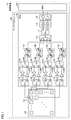
- FIG. 1 is a block diagram of an example of a communication device 10 to which an antenna module 100 according to the present embodiment is applied.
- the communication device 10 is, for example, a mobile terminal such as a mobile phone, a smartphone or a tablet, or a personal computer having a communication function.
- the communication device 10 includes an antenna module 100 and a BBIC 200 that constitutes a baseband signal processing circuit.
- the antenna module 100 includes an RFIC (Radio Frequency Integrated Circuit) 110 that is an example of a high-frequency element, and an antenna array 120.
- the communication device 10 up-converts the signal transmitted from the BBIC 200 to the antenna module 100 and radiates it from the antenna array 120, and down-converts the high-frequency signal received by the antenna array 120 and processes the signal by the BBIC 200. .
- RFIC Radio Frequency Integrated Circuit
- FIG. 1 for ease of explanation, only a configuration corresponding to four antenna elements (radiating elements) 121 among a plurality of antenna elements 121 configuring the antenna array 120 is shown and has the same configuration. The configuration corresponding to the other antenna elements 121 is omitted.
- the RFIC 110 includes switches 111A to 111D, 113A to 113D, 117, power amplifiers 112AT to 112DT, low noise amplifiers 112AR to 112DR, attenuators 114A to 114D, phase shifters 115A to 115D, and a signal synthesizer / demultiplexer. 116, a mixer 118, and an amplifier circuit 119.
- the switches 111A to 111D and 113A to 113D are switched to the power amplifiers 112AT to 112DT side, and the switch 117 is connected to the transmission side amplifier of the amplifier circuit 119.
- the switches 111A to 111D and 113A to 113D are switched to the low noise amplifiers 112AR to 112DR side, and the switch 117 is connected to the reception side amplifier of the amplifier circuit 119.
- the signal transmitted from the BBIC 200 is amplified by the amplifier circuit 119 and up-converted by the mixer 118.
- the up-converted transmission signal which is a high-frequency signal, is demultiplexed by the signal synthesizer / demultiplexer 116, passes through four signal paths, and is fed to different antenna elements 121.
- the directivity of the antenna array 120 can be adjusted by individually adjusting the degree of phase shift of the phase shifters 115A to 115D arranged in each signal path.
- the received signals that are high-frequency signals received by the antenna elements 121 are multiplexed by the signal synthesizer / demultiplexer 116 via four different signal paths.
- the combined received signal is down-converted by mixer 118, amplified by amplifier circuit 119, and transmitted to BBIC 200.
- the RFIC 110 is formed, for example, as a one-chip integrated circuit component including the above circuit configuration.
- the devices switching, power amplifiers, low noise amplifiers, attenuators, phase shifters
- the RFIC 110 may be formed as one chip integrated circuit components for each corresponding antenna element 121. .
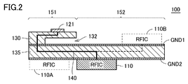
- FIG. 2 is a cross-sectional view of a first example of the antenna module according to the first embodiment.
- antenna module 100 includes a first dielectric layer 130, a second dielectric layer 135, and ground electrodes GND1 and GND2, in addition to antenna element 121 and RFIC 110.
- GND1 and GND2 ground electrodes
- FIG. 2 for ease of explanation, a case where only one antenna element 121 is arranged will be described, but a plurality of antenna elements 121 may be arranged.
- the first dielectric layer 130 and the second dielectric layer 135 are formed of, for example, a resin such as epoxy or polyimide.
- the dielectric layer may be formed using a liquid crystal polymer (LCP) or a fluorine resin having a lower dielectric constant.
- the second dielectric layer 135 is formed, for example, in a flat plate shape, and ground electrodes GND1 and GND2 are laminated on the front and back surfaces, respectively.
- the first dielectric layer 130 is partially disposed on the ground electrode GND1, and the antenna element 121 is disposed on the surface thereof.
- a portion where the first dielectric layer 130 is disposed that is, a portion where the thickness in the normal direction is thick
- the portion 151 having no thickness in the normal direction without the first dielectric layer 130 is also referred to as a second portion 152.
- second portion 152 By thinning the portion where the antenna element is not disposed (second portion 152), it is possible to contribute to high integration of the entire device on which the antenna module is mounted.
- the RFIC 110 is disposed so as to be in contact with the ground electrode GND2.
- the high frequency signal output from the RFIC 110 is transmitted to the antenna element 121 through the feeder line 140.
- the feeder 140 is connected to the antenna element 121 through the second dielectric layer 135 and further through the first dielectric layer 130.
- the RFIC 110 is disposed in the second portion 152 of the ground electrode GND2, but may be disposed in the first portion 151 (broken line portion 110A in FIG. 2). Further, an RFIC may be disposed on the ground electrode GND1 on the same side as the first dielectric layer 130 (broken line portion 110B in FIG. 2).
- a space 132 is partially formed in the first dielectric layer 130 in the thickness direction (the normal direction of the dielectric layer).
- the antenna element 121 is arranged so that at least a part thereof overlaps with a region where the space 132 is formed when the dielectric layer is viewed in plan. It is more preferable that the entire antenna element 121 overlaps the space 132.
- the lower surface of the space 132 in the first portion 151 is the ground electrode GND1, and is continuous with the upper surface of the second portion 152.
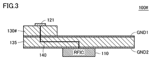
- FIG. 3 is a cross-sectional view of the antenna module 100 # of the comparative example.
- the antenna module 100 # in FIG. 3 has a configuration in which the first dielectric layer 130 in the antenna module 100 in FIG. 2 is replaced with the first dielectric layer 130 #.
- the first dielectric layer 130 # is solid, and the space 132 is not formed like the first dielectric layer 130 of FIG.
- the characteristics of the antenna module in general, it is required to increase the frequency bandwidth that can be transmitted and received and to reduce the loss when transmitting a high-frequency signal.
- the loss characteristics of the antenna it is generally known that the lower the relative dielectric constant ( ⁇ r) and the dielectric loss tangent (tan ⁇ ) of the dielectric layer in which the antenna element is arranged, the better. In order to reduce the power consumption of the device, it is necessary to reduce the dielectric constant of the dielectric layer.
- the bandwidth of the dielectric layer that is, the distance between the antenna element and the ground electrode
- the bandwidth the greater the thickness of the dielectric layer (that is, the distance between the antenna element and the ground electrode)
- the antenna module itself needs to be thinned.
- the dielectric layer is made thin in order to realize a reduction in thickness, the frequency bandwidth of the antenna may be reduced.
- the antenna module 100 # in the comparative example of FIG. 3 in order to ensure a wide frequency bandwidth, it is necessary to increase the thickness of the first dielectric layer 130 # in the normal direction. However, in that case, the height of the antenna module becomes high, which does not match the needs for thinning.
- the antenna element 121 and the ground electrode GND1 in the first dielectric layer 130 where the antenna element 121 is disposed since the space 132 is formed between the antenna element 121 and the ground electrode GND1 in the first dielectric layer 130 where the antenna element 121 is disposed, the antenna element Even if the distance between 121 and the ground electrode GND1 is the same as in the comparative example of FIG. 3, the effective dielectric constant between the antenna element 121 and the ground electrode GND1 can be further reduced. Therefore, by providing the space 132 in the first dielectric layer 130 in which the antenna element 121 is disposed, it is possible to improve the frequency bandwidth and reduce the loss.
- the effective dielectric constant between the antenna element 121 and the ground electrode GND1 can be reduced by forming the space 132 in the first dielectric layer 130 as in the first embodiment, the frequency bandwidth and the antenna gain are improved. can do. Alternatively, it is possible to reduce the effective dielectric constant and reduce the height by reducing the thickness of the first dielectric layer 130.
- FIG. 4 is a cross-sectional view of a second example of the antenna module according to the first embodiment.
- a third dielectric layer 130A disposed on the ground electrode GND1 is provided, and on the third dielectric layer 130A.
- An antenna element 121A is further arranged. A high frequency signal is transmitted to the antenna element 121A via the feeder line 140A.
- a portion where the third dielectric layer 130A is disposed is referred to as a third portion 153.
- the third portion 153 of FIG. 4 no space is provided in the third dielectric layer 130 ⁇ / b> A, but a space may be provided in the same manner as the first dielectric layer 130.
- the RFIC 110 is disposed so as to be in contact with the second portion 152 of the ground electrode GND2. However, the RFIC 110 may be disposed on the first portion 151 or the third portion 153 of the ground electrode GND2.
- the cross section of the first dielectric layer 130 is L-shaped as in FIG. 2, and is attached on the ground electrode GND ⁇ b> 1 by one support portion 131.
- the first dielectric layer 130 extends in a plane direction orthogonal to the direction from the first portion 151 toward the second portion 152, and includes a plurality of (FIG. 5).
- the four antenna elements 121 are spaced apart at substantially equal intervals.
- the first dielectric layer 130B is an example of the first dielectric layer 130B having a C-shaped cross section.
- the first dielectric layer 130B is mounted on the ground electrode GND1 by two support portions 131B extending in the arrangement direction of the antenna elements 121 in FIG. 6A, and a space 132B is provided between the two support portions 131B. Is formed.
- first dielectric layer 130 ⁇ / b> C in FIG. 7 support portions are formed along three sides of each rectangular antenna element 121, and a space 132 ⁇ / b> C is individually formed for each antenna element 121. Yes.
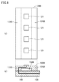
- FIG. 8 is an example in which a plurality of antenna elements 121 are two-dimensionally arranged, and in FIG. 8, 8 antenna elements 121 of 2 ⁇ 4 are arranged.
- the first dielectric layer 130 ⁇ / b> D support portions are formed along the four sides of each rectangular antenna element 121, and a space 132 ⁇ / b> D is individually formed for each antenna element 121.
- each antenna element 121 when viewed in plan from the normal direction of the dielectric layer, each antenna element 121 entirely overlaps the space 132, but the antenna element 121 and the support portion are partially overlapped. May overlap. However, even in that case, from the viewpoint of the directivity of the antenna, it is preferable that the overlapping portion of the antenna element 121 and the support portion is symmetrical when viewed in plan and is the same for each antenna element 121.
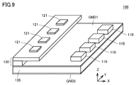
- FIG. 9 is a perspective view of an example of an antenna module when the first dielectric layer having the structure of FIG. 5 is used. As shown in FIG. 9, the plurality of antenna elements 121 are arranged separately on the first dielectric layer 130 extending in the Y direction in FIG. 9.
- the RFIC 110 is arranged on the ground electrode GND1 spaced in the X direction in FIG. Each RFIC 110 transmits a high-frequency signal to the corresponding antenna element 121.
- the antenna module by providing a space between the antenna element and the ground electrode in the portion of the dielectric layer where the antenna element is disposed, it is effective while ensuring the distance between the antenna element and the ground electrode.
- the dielectric constant can be reduced.
- the antenna performance can be improved by reducing the loss while maintaining the frequency bandwidth.
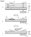
- FIG. 10 is a diagram for explaining a first example of a manufacturing process of the antenna module 100A of FIG.
- the ground electrode GND1 and the ground electrode GND2 are stacked on the front surface and the back surface of the second dielectric layer 135.
- the first dielectric layer 130 is formed by laminating the first layer 130_1 on which the antenna elements 121 and 121A are arranged and the second layer 130_2 on which the space 132 is formed. First, the second layer 130_2 is stacked on the ground electrode GND1. At this time, a member 150 made of a material different from that of the first dielectric layer 130, such as stainless steel, is disposed in a portion forming the space 132.
- the first layer 130_1 is stacked on the second layer 130_2, and the antenna elements 121 and 121A are disposed on the first layer 130_1.
- the RFIC 110 is disposed on the ground electrode GND2 on the back surface side of the second dielectric layer 135.
- the ground electrode GND2 is exposed by laser processing or cutting of the first layer 130_1 and the second layer 130_2 corresponding to the second portion 152 of FIG. Is removed.
- the member 150 may be formed of a soluble resin and chemically removed by etching.
- the layers are sequentially laminated in a state where the member 150 made of a material different from the first dielectric layer 130 is disposed in the portion where the space 132 is to be formed, and the second portion 152 After removing the first dielectric layer 130 corresponding to, the space 150 is formed by removing the member 150 from the space 155 that has been removed.
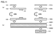
- FIG. 11 is a diagram illustrating a second example of the manufacturing process of the antenna module 100A.
- the antenna module 100 ⁇ / b> A is manufactured by only the lamination process without using the removal process of the first dielectric layer 130 and the extraction process of the member 150 as shown in FIG. 10 will be described.
- the first portion 151 is formed by laminating the main body portion 133 and the support portion 131 of the first dielectric layer 130 on the antenna element 121.
- the third portion 153 is formed by laminating the main body portion 133A of the first dielectric layer 130A and the support portion 131A on the antenna element 121A. Note that the third portion 153 may be formed as one member instead of the laminated structure of the main body portion 133A and the support portion 131A.
- the top and bottom of the first portion 151 of the first dielectric layer 130 and the third portion 153 of the first dielectric layer 130A formed in FIG. It is laminated on the ground electrode GND1.
- the RFIC 110 is disposed on the ground electrode GND ⁇ b> 2 on the back surface side of the second dielectric layer 135.
- the main body portion and the support portion of the first dielectric layer are stacked on the antenna elements 121 and 121A, and they are turned upside down to be stacked on the second dielectric layer 135. 132 is formed. Therefore, the space 132 can be formed without using the removal process of the first dielectric layer by laser processing or the like and the extraction process of the member 150 arranged in advance in the part where the space 132 is formed.
- FIG. 12 is a diagram for explaining a third example of the manufacturing process of the antenna module 100A.
- the first portion 151 with the space 132 is formed by bending an end portion of a flexible flat dielectric layer (flexible substrate) will be described.
- ground electrodes GND1 and GND2 are respectively stacked on the front and back surfaces of portions other than the end 136 of the flat dielectric layer 130E. Thereafter, as shown in FIG. 12B, the end 136 is bent so that the space 132 is formed between the ground electrode GND1 and the first portion 151 of FIG. 4 is formed. And the antenna element 121 is arrange
- the third portion 153 is formed by stacking the third dielectric layer 130A on the ground electrode GND1 and further stacking the antenna element 121A thereon. Then, the RFIC 110 is disposed on the ground electrode GND2 (FIG. 10C).
- the third portion is formed by a laminated structure, but it may be formed by bending the other end of the dielectric layer in the same manner as the first portion. At this time, if a space like the first portion is unnecessary, the bent dielectric layer and the ground electrode GND1 are brought into close contact with each other.
- the end of the dielectric layer is bent while maintaining a space with the ground electrode GND1, and the portion corresponding to the first dielectric layer is formed by facing the ground electrode. It is formed.
- FIG. 13 is a diagram for explaining an arrangement example of the antenna module 100A in the communication device 10 in which the antenna module 100A of FIG. 4 is mounted.
- the RFIC 110 of the antenna module 100A is connected to the mounting substrate 50 via a solder bump or the like (not shown) on the surface opposite to the second dielectric layer 135.
- the mounting substrate 50 not only functions as a substrate for fixing the antenna module 100A, but also functions as a heat sink for releasing heat generated in the RFIC 110.
- the antenna elements 121 and 121A of the antenna module 100A are arranged at positions close to the casing 20 of the communication device 10 in order to radiate radio waves to the outside of the communication device 10 and to receive radio waves from the outside.
- a metal material can function as a shield against radio waves
- a resin portion 30 formed of a resin that can pass radio waves is partially formed.
- the antenna elements 121 and 121A are arranged so as to face the resin part 30. Accordingly, it is possible to appropriately transmit and receive radio waves without being affected by the metal casing. There may be a gap between each antenna element 121, 121A, 121B and the resin portion 35, 35A.
- the antenna elements 121 and 121A can be arrange
- the dielectric layer on which the antenna element is arranged has a substantially rectangular shape when viewed in plan, and for example, the configuration in which the two antenna elements in FIG. 4 are arranged in a straight line has been described. .
- the antenna module is used for a small and thin communication device such as a smartphone, and may be required to be arranged in a limited space in the device. In this case, depending on the mounting location of the antenna module, it may be necessary to offset the two antenna elements. Then, in the linear antenna arrangement, mechanical stress is applied to the dielectric layer, and there is a possibility that the dielectric layer is cracked.
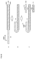
- FIG. 14 is a diagram for illustrating antenna module 100B according to the second embodiment.
- FIG. 14A shows a cross-sectional view
- FIG. 14B shows a plan view.
- the second dielectric layer 135 is replaced with the second dielectric layer 135B and the RFIC 110 is disposed in the third portion 153 as compared with the antenna module 100A described in FIG.
- the other points are the same as in FIG. Therefore, the description of the same part in FIG. 14 as that in FIG. 4 will not be repeated.
- the second dielectric layer 135 ⁇ / b> B is a direction orthogonal to the extending direction from the first portion 151 toward the second portion 152 when viewed in plan (FIG. 14B). Is bent. That is, it is bent in a substantially S shape from the first portion 151 toward the third portion 153. Thereby, the antenna element 121 and the antenna element 121A can be arranged in an offset state.
- the offset amount is designed according to the device on which the antenna module 100B is mounted.
- the bending start point SP on the first portion 151 side is set in the space 132 in the first portion 151.
- the curvature of the bent portion of the second dielectric layer 135B can be made gentler than the starting point is the boundary between the first portion 151 and the second portion 152. Therefore, mechanical stress applied to the second dielectric layer 135B can be reduced when the antenna module 100B is attached.
- the configuration in which the radiation electrode is disposed on the surface of the dielectric layer has been described as an example.
- the radiation electrode may be disposed in the dielectric layer. That is, the radiation electrode may not be exposed from the dielectric layer, and may be covered with a cover lay which is a resist or thin film dielectric layer.
- the ground electrode may be formed inside the dielectric layer.
- dielectric layers 130E, 135, and 135B through which the feed line from the RFIC 110 passes forms a strip line in which ground electrodes are arranged on both surfaces of the dielectric layer.
- these dielectric layers are formed as a microstrip line in which a ground electrode is disposed only on one side of the dielectric layer, or a coplanar line in which the ground electrode and the feed line are disposed in the same layer in the dielectric layer. May be.
- 10 communication device 20 housing, 30 resin part, 50 mounting board, 100, 100A, 100B, 100 # antenna module, 110, 110A, 110B RFIC, 111A-111D, 113A-113D, 117 switch, 112AR-112DR low noise amplifier , 112AT-112DT power amplifier, 114A-114D attenuator, 115A-115D phase shifter, 116 signal synthesizer / demultiplexer, 118 mixer, 119 amplifier circuit, 120 antenna array, 121, 121A antenna element, 130, 130_1, 130_2 , 130A, 130B, 130D, 130 #, 130E, 135, 135B dielectric layer, 131, 131A, 131B support, 132, 132B, 132C, 132D, 155 space, 1 3,133A body portion 136 ends, 140 and 140A feed line, 150 members, 151 first portion 152 second portion 153 third portion, GND1, GND2 ground electrode, SP bending start point.
Landscapes
- Engineering & Computer Science (AREA)
- Microelectronics & Electronic Packaging (AREA)
- Details Of Aerials (AREA)
- Support Of Aerials (AREA)
- Variable-Direction Aerials And Aerial Arrays (AREA)
Abstract
La présente invention concerne un module d'antenne (100) équipé d'un ou de plusieurs éléments d'antenne (121), d'une électrode de masse (GND1) et d'une couche diélectrique (130) ayant les éléments d'antenne (121) installés sur celle-ci et disposés entre les éléments d'antenne (121) et l'électrode de masse (GND1). Lorsque la couche diélectrique (130) est vue depuis une vue en plan, un espace (132) est formé entre la couche diélectrique (130) et l'électrode de masse (GND1) dans une région où les éléments d'antenne (121) et l'électrode de masse (GND1) se chevauchent.
Priority Applications (2)
| Application Number | Priority Date | Filing Date | Title |
|---|---|---|---|
| CN201980014514.3A CN111788740B (zh) | 2018-02-22 | 2019-01-23 | 天线模块和搭载有天线模块的通信装置 |
| US16/992,463 US11450942B2 (en) | 2018-02-22 | 2020-08-13 | Antenna module and communication device equipped with the same |
Applications Claiming Priority (2)
| Application Number | Priority Date | Filing Date | Title |
|---|---|---|---|
| JP2018029845 | 2018-02-22 | ||
| JP2018-029845 | 2018-02-22 |
Related Child Applications (1)
| Application Number | Title | Priority Date | Filing Date |
|---|---|---|---|
| US16/992,463 Continuation US11450942B2 (en) | 2018-02-22 | 2020-08-13 | Antenna module and communication device equipped with the same |
Publications (1)
| Publication Number | Publication Date |
|---|---|
| WO2019163376A1 true WO2019163376A1 (fr) | 2019-08-29 |
Family
ID=67687646
Family Applications (1)
| Application Number | Title | Priority Date | Filing Date |
|---|---|---|---|
| PCT/JP2019/002029 WO2019163376A1 (fr) | 2018-02-22 | 2019-01-23 | Module d'antenne et dispositif de communication disposant du module d'antenne en son sein |
Country Status (3)
| Country | Link |
|---|---|
| US (1) | US11450942B2 (fr) |
| CN (1) | CN111788740B (fr) |
| WO (1) | WO2019163376A1 (fr) |
Cited By (1)
| Publication number | Priority date | Publication date | Assignee | Title |
|---|---|---|---|---|
| US12003012B2 (en) | 2020-01-27 | 2024-06-04 | Murata Manufacturing Co., Ltd. | Antenna module |
Families Citing this family (6)
| Publication number | Priority date | Publication date | Assignee | Title |
|---|---|---|---|---|
| US11088468B2 (en) * | 2017-12-28 | 2021-08-10 | Samsung Electro-Mechanics Co., Ltd. | Antenna module |
| CN110212300B (zh) * | 2019-05-22 | 2021-05-11 | 维沃移动通信有限公司 | 一种天线单元及终端设备 |
| KR102272590B1 (ko) | 2019-06-21 | 2021-07-05 | 삼성전기주식회사 | 안테나 모듈 및 이를 포함하는 전자기기 |
| KR102593888B1 (ko) * | 2019-06-13 | 2023-10-24 | 삼성전기주식회사 | 안테나 모듈 및 이를 포함하는 전자기기 |
| US11335991B2 (en) * | 2019-11-13 | 2022-05-17 | Samsung Electro-Mechanics Co., Ltd. | Electronic device with radio-frequency module |
| JP7209314B2 (ja) * | 2019-11-13 | 2023-01-20 | 国立大学法人埼玉大学 | アンテナモジュールおよびそれを搭載した通信装置 |
Citations (3)
| Publication number | Priority date | Publication date | Assignee | Title |
|---|---|---|---|---|
| JPH05152831A (ja) * | 1991-11-29 | 1993-06-18 | Toko Inc | マイクロストリツプアンテナの共振周波数調整方法 |
| JP2005051329A (ja) * | 2003-07-29 | 2005-02-24 | Furukawa Electric Co Ltd:The | 二周波共用平面パッチアンテナ及び多周波共用平面パッチアンテナ |
| WO2016063759A1 (fr) * | 2014-10-20 | 2016-04-28 | 株式会社村田製作所 | Module de communication sans fil |
Family Cites Families (16)
| Publication number | Priority date | Publication date | Assignee | Title |
|---|---|---|---|---|
| JPH06283924A (ja) | 1993-03-30 | 1994-10-07 | Tokimec Inc | マイクロストリップアレイアンテナ |
| JPH08222940A (ja) * | 1995-02-14 | 1996-08-30 | Mitsubishi Electric Corp | アンテナ装置 |
| US5696517A (en) * | 1995-09-28 | 1997-12-09 | Murata Manufacturing Co., Ltd. | Surface mounting antenna and communication apparatus using the same |
| JPH09307342A (ja) * | 1996-05-14 | 1997-11-28 | Mitsubishi Electric Corp | アンテナ装置 |
| JP2000295030A (ja) * | 1999-04-06 | 2000-10-20 | Nec Corp | 高周波装置およびその製造方法 |
| US20020075186A1 (en) * | 2000-12-20 | 2002-06-20 | Hiroki Hamada | Chip antenna and method of manufacturing the same |
| JP2003087022A (ja) * | 2001-09-07 | 2003-03-20 | Tdk Corp | アンテナモジュールおよびそれを用いた電子装置 |
| US7068230B2 (en) * | 2004-06-02 | 2006-06-27 | Research In Motion Limited | Mobile wireless communications device comprising multi-frequency band antenna and related methods |
| US7274334B2 (en) * | 2005-03-24 | 2007-09-25 | Tdk Corporation | Stacked multi-resonator antenna |
| CN102332635B (zh) * | 2010-04-07 | 2013-12-25 | 庄昆杰 | 微波低波段多频带高增益双极化小型微带天线 |
| JP5727587B2 (ja) * | 2010-09-07 | 2015-06-03 | 昆 杰 庄 | 二偏波マイクロストリップアンテナ |
| JP2013187731A (ja) | 2012-03-08 | 2013-09-19 | Mitsubishi Electric Corp | アンテナ装置 |
| CN107078406B (zh) | 2014-10-31 | 2021-07-23 | 株式会社村田制作所 | 天线模块以及电路模块 |
| CN104600419B (zh) * | 2015-01-05 | 2018-11-06 | 北京邮电大学 | 径向线馈电介质谐振天线阵列 |
| CN104836027A (zh) * | 2015-05-24 | 2015-08-12 | 五邑大学 | 波束赋形超高频射频识别读写器天线线阵 |
| US10685924B2 (en) * | 2017-08-24 | 2020-06-16 | Qualcomm Incorporated | Antenna-on-package arrangements |
-
2019
- 2019-01-23 CN CN201980014514.3A patent/CN111788740B/zh active Active
- 2019-01-23 WO PCT/JP2019/002029 patent/WO2019163376A1/fr active Application Filing
-
2020
- 2020-08-13 US US16/992,463 patent/US11450942B2/en active Active
Patent Citations (3)
| Publication number | Priority date | Publication date | Assignee | Title |
|---|---|---|---|---|
| JPH05152831A (ja) * | 1991-11-29 | 1993-06-18 | Toko Inc | マイクロストリツプアンテナの共振周波数調整方法 |
| JP2005051329A (ja) * | 2003-07-29 | 2005-02-24 | Furukawa Electric Co Ltd:The | 二周波共用平面パッチアンテナ及び多周波共用平面パッチアンテナ |
| WO2016063759A1 (fr) * | 2014-10-20 | 2016-04-28 | 株式会社村田製作所 | Module de communication sans fil |
Cited By (1)
| Publication number | Priority date | Publication date | Assignee | Title |
|---|---|---|---|---|
| US12003012B2 (en) | 2020-01-27 | 2024-06-04 | Murata Manufacturing Co., Ltd. | Antenna module |
Also Published As
| Publication number | Publication date |
|---|---|
| CN111788740A (zh) | 2020-10-16 |
| US20200373646A1 (en) | 2020-11-26 |
| US11450942B2 (en) | 2022-09-20 |
| CN111788740B (zh) | 2023-05-02 |
Similar Documents
| Publication | Publication Date | Title |
|---|---|---|
| WO2019163376A1 (fr) | Module d'antenne et dispositif de communication disposant du module d'antenne en son sein | |
| US11611147B2 (en) | Antenna module, communication device equipped with the same, and manufacturing method of antenna module | |
| CN112640209B (zh) | 天线模块以及搭载有该天线模块的通信装置 | |
| CN111742447B (zh) | 天线模块和搭载有天线模块的通信装置 | |
| US11539122B2 (en) | Antenna module and communication unit provided with the same | |
| CN114521307B (zh) | 天线模块和搭载该天线模块的通信装置以及电路基板 | |
| US11888245B2 (en) | Flexible substrate and antenna module including flexible substrate | |
| US11322841B2 (en) | Antenna module and communication device equipped with the same | |
| US20220181794A1 (en) | Antenna device, antenna module, and communication device | |
| WO2021153034A1 (fr) | Module d'antenne | |
| WO2021059738A1 (fr) | Module d'antenne et son procédé de fabrication, et substrat à agrégat | |
| US11916312B2 (en) | Antenna module, communication device mounting the same, and circuit board | |
| WO2023210118A1 (fr) | Module d'antenne | |
| US20220085521A1 (en) | Antenna module and communication device equipped with the same | |
| WO2023157450A1 (fr) | Module d'antenne et dispositif de communication avec ce module d'antenne monté dessus | |
| CN115004476B (zh) | 天线装置 | |
| WO2022230427A1 (fr) | Dispositif d'antenne | |
| US20220328983A1 (en) | Antenna module and communication device equipped with the same | |
| US12003012B2 (en) | Antenna module | |
| WO2021019899A1 (fr) | Dispositif d'antenne, module d'antenne et dispositif de communication | |
| WO2022185874A1 (fr) | Module d'antenne et dispositif de communication équipé de ce dernier | |
| US20240178567A1 (en) | Antenna module and communication apparatus equipped with the same | |
| US20240047883A1 (en) | Antenna module and communication apparatus equipped with the same | |
| CN116097180A (zh) | 通信装置 |
Legal Events
| Date | Code | Title | Description |
|---|---|---|---|
| 121 | Ep: the epo has been informed by wipo that ep was designated in this application |
Ref document number: 19757324 Country of ref document: EP Kind code of ref document: A1 |
|
| NENP | Non-entry into the national phase |
Ref country code: DE |
|
| 122 | Ep: pct application non-entry in european phase |
Ref document number: 19757324 Country of ref document: EP Kind code of ref document: A1 |
|
| NENP | Non-entry into the national phase |
Ref country code: JP |