WO2019155959A1 - Method for manufacturing semiconductor device - Google Patents
Method for manufacturing semiconductor device Download PDFInfo
- Publication number
- WO2019155959A1 WO2019155959A1 PCT/JP2019/003169 JP2019003169W WO2019155959A1 WO 2019155959 A1 WO2019155959 A1 WO 2019155959A1 JP 2019003169 W JP2019003169 W JP 2019003169W WO 2019155959 A1 WO2019155959 A1 WO 2019155959A1
- Authority
- WO
- WIPO (PCT)
- Prior art keywords
- support substrate
- semiconductor device
- layer
- manufacturing
- forming
- Prior art date
Links
Images


Classifications
-
- H—ELECTRICITY
- H01—ELECTRIC ELEMENTS
- H01L—SEMICONDUCTOR DEVICES NOT COVERED BY CLASS H10
- H01L24/00—Arrangements for connecting or disconnecting semiconductor or solid-state bodies; Methods or apparatus related thereto
- H01L24/01—Means for bonding being attached to, or being formed on, the surface to be connected, e.g. chip-to-package, die-attach, "first-level" interconnects; Manufacturing methods related thereto
- H01L24/18—High density interconnect [HDI] connectors; Manufacturing methods related thereto
- H01L24/19—Manufacturing methods of high density interconnect preforms
-
- H—ELECTRICITY
- H01—ELECTRIC ELEMENTS
- H01L—SEMICONDUCTOR DEVICES NOT COVERED BY CLASS H10
- H01L23/00—Details of semiconductor or other solid state devices
- H01L23/12—Mountings, e.g. non-detachable insulating substrates
- H01L23/13—Mountings, e.g. non-detachable insulating substrates characterised by the shape
-
- H—ELECTRICITY
- H01—ELECTRIC ELEMENTS
- H01L—SEMICONDUCTOR DEVICES NOT COVERED BY CLASS H10
- H01L21/00—Processes or apparatus adapted for the manufacture or treatment of semiconductor or solid state devices or of parts thereof
- H01L21/67—Apparatus specially adapted for handling semiconductor or electric solid state devices during manufacture or treatment thereof; Apparatus specially adapted for handling wafers during manufacture or treatment of semiconductor or electric solid state devices or components ; Apparatus not specifically provided for elsewhere
- H01L21/683—Apparatus specially adapted for handling semiconductor or electric solid state devices during manufacture or treatment thereof; Apparatus specially adapted for handling wafers during manufacture or treatment of semiconductor or electric solid state devices or components ; Apparatus not specifically provided for elsewhere for supporting or gripping
- H01L21/6835—Apparatus specially adapted for handling semiconductor or electric solid state devices during manufacture or treatment thereof; Apparatus specially adapted for handling wafers during manufacture or treatment of semiconductor or electric solid state devices or components ; Apparatus not specifically provided for elsewhere for supporting or gripping using temporarily an auxiliary support
-
- H—ELECTRICITY
- H01—ELECTRIC ELEMENTS
- H01L—SEMICONDUCTOR DEVICES NOT COVERED BY CLASS H10
- H01L21/00—Processes or apparatus adapted for the manufacture or treatment of semiconductor or solid state devices or of parts thereof
- H01L21/02—Manufacture or treatment of semiconductor devices or of parts thereof
- H01L21/04—Manufacture or treatment of semiconductor devices or of parts thereof the devices having at least one potential-jump barrier or surface barrier, e.g. PN junction, depletion layer or carrier concentration layer
- H01L21/50—Assembly of semiconductor devices using processes or apparatus not provided for in a single one of the subgroups H01L21/06 - H01L21/326, e.g. sealing of a cap to a base of a container
- H01L21/56—Encapsulations, e.g. encapsulation layers, coatings
- H01L21/561—Batch processing
-
- H—ELECTRICITY
- H01—ELECTRIC ELEMENTS
- H01L—SEMICONDUCTOR DEVICES NOT COVERED BY CLASS H10
- H01L21/00—Processes or apparatus adapted for the manufacture or treatment of semiconductor or solid state devices or of parts thereof
- H01L21/70—Manufacture or treatment of devices consisting of a plurality of solid state components formed in or on a common substrate or of parts thereof; Manufacture of integrated circuit devices or of parts thereof
- H01L21/71—Manufacture of specific parts of devices defined in group H01L21/70
- H01L21/76—Making of isolation regions between components
-
- H—ELECTRICITY
- H01—ELECTRIC ELEMENTS
- H01L—SEMICONDUCTOR DEVICES NOT COVERED BY CLASS H10
- H01L21/00—Processes or apparatus adapted for the manufacture or treatment of semiconductor or solid state devices or of parts thereof
- H01L21/70—Manufacture or treatment of devices consisting of a plurality of solid state components formed in or on a common substrate or of parts thereof; Manufacture of integrated circuit devices or of parts thereof
- H01L21/77—Manufacture or treatment of devices consisting of a plurality of solid state components or integrated circuits formed in, or on, a common substrate
- H01L21/78—Manufacture or treatment of devices consisting of a plurality of solid state components or integrated circuits formed in, or on, a common substrate with subsequent division of the substrate into plural individual devices
-
- H—ELECTRICITY
- H01—ELECTRIC ELEMENTS
- H01L—SEMICONDUCTOR DEVICES NOT COVERED BY CLASS H10
- H01L23/00—Details of semiconductor or other solid state devices
- H01L23/28—Encapsulations, e.g. encapsulating layers, coatings, e.g. for protection
-
- H—ELECTRICITY
- H01—ELECTRIC ELEMENTS
- H01L—SEMICONDUCTOR DEVICES NOT COVERED BY CLASS H10
- H01L23/00—Details of semiconductor or other solid state devices
- H01L23/32—Holders for supporting the complete device in operation, i.e. detachable fixtures
-
- H—ELECTRICITY
- H01—ELECTRIC ELEMENTS
- H01L—SEMICONDUCTOR DEVICES NOT COVERED BY CLASS H10
- H01L23/00—Details of semiconductor or other solid state devices
- H01L23/48—Arrangements for conducting electric current to or from the solid state body in operation, e.g. leads, terminal arrangements ; Selection of materials therefor
- H01L23/482—Arrangements for conducting electric current to or from the solid state body in operation, e.g. leads, terminal arrangements ; Selection of materials therefor consisting of lead-in layers inseparably applied to the semiconductor body
- H01L23/485—Arrangements for conducting electric current to or from the solid state body in operation, e.g. leads, terminal arrangements ; Selection of materials therefor consisting of lead-in layers inseparably applied to the semiconductor body consisting of layered constructions comprising conductive layers and insulating layers, e.g. planar contacts
-
- H—ELECTRICITY
- H01—ELECTRIC ELEMENTS
- H01L—SEMICONDUCTOR DEVICES NOT COVERED BY CLASS H10
- H01L23/00—Details of semiconductor or other solid state devices
- H01L23/52—Arrangements for conducting electric current within the device in operation from one component to another, i.e. interconnections, e.g. wires, lead frames
- H01L23/522—Arrangements for conducting electric current within the device in operation from one component to another, i.e. interconnections, e.g. wires, lead frames including external interconnections consisting of a multilayer structure of conductive and insulating layers inseparably formed on the semiconductor body
- H01L23/525—Arrangements for conducting electric current within the device in operation from one component to another, i.e. interconnections, e.g. wires, lead frames including external interconnections consisting of a multilayer structure of conductive and insulating layers inseparably formed on the semiconductor body with adaptable interconnections
-
- H—ELECTRICITY
- H05—ELECTRIC TECHNIQUES NOT OTHERWISE PROVIDED FOR
- H05K—PRINTED CIRCUITS; CASINGS OR CONSTRUCTIONAL DETAILS OF ELECTRIC APPARATUS; MANUFACTURE OF ASSEMBLAGES OF ELECTRICAL COMPONENTS
- H05K3/00—Apparatus or processes for manufacturing printed circuits
-
- H—ELECTRICITY
- H05—ELECTRIC TECHNIQUES NOT OTHERWISE PROVIDED FOR
- H05K—PRINTED CIRCUITS; CASINGS OR CONSTRUCTIONAL DETAILS OF ELECTRIC APPARATUS; MANUFACTURE OF ASSEMBLAGES OF ELECTRICAL COMPONENTS
- H05K3/00—Apparatus or processes for manufacturing printed circuits
- H05K3/46—Manufacturing multilayer circuits
-
- H—ELECTRICITY
- H01—ELECTRIC ELEMENTS
- H01L—SEMICONDUCTOR DEVICES NOT COVERED BY CLASS H10
- H01L21/00—Processes or apparatus adapted for the manufacture or treatment of semiconductor or solid state devices or of parts thereof
- H01L21/02—Manufacture or treatment of semiconductor devices or of parts thereof
- H01L21/04—Manufacture or treatment of semiconductor devices or of parts thereof the devices having at least one potential-jump barrier or surface barrier, e.g. PN junction, depletion layer or carrier concentration layer
- H01L21/50—Assembly of semiconductor devices using processes or apparatus not provided for in a single one of the subgroups H01L21/06 - H01L21/326, e.g. sealing of a cap to a base of a container
- H01L21/56—Encapsulations, e.g. encapsulation layers, coatings
- H01L21/568—Temporary substrate used as encapsulation process aid
-
- H—ELECTRICITY
- H01—ELECTRIC ELEMENTS
- H01L—SEMICONDUCTOR DEVICES NOT COVERED BY CLASS H10
- H01L2221/00—Processes or apparatus adapted for the manufacture or treatment of semiconductor or solid state devices or of parts thereof covered by H01L21/00
- H01L2221/67—Apparatus for handling semiconductor or electric solid state devices during manufacture or treatment thereof; Apparatus for handling wafers during manufacture or treatment of semiconductor or electric solid state devices or components; Apparatus not specifically provided for elsewhere
- H01L2221/683—Apparatus for handling semiconductor or electric solid state devices during manufacture or treatment thereof; Apparatus for handling wafers during manufacture or treatment of semiconductor or electric solid state devices or components; Apparatus not specifically provided for elsewhere for supporting or gripping
- H01L2221/68304—Apparatus for handling semiconductor or electric solid state devices during manufacture or treatment thereof; Apparatus for handling wafers during manufacture or treatment of semiconductor or electric solid state devices or components; Apparatus not specifically provided for elsewhere for supporting or gripping using temporarily an auxiliary support
- H01L2221/68318—Auxiliary support including means facilitating the separation of a device or wafer from the auxiliary support
-
- H—ELECTRICITY
- H01—ELECTRIC ELEMENTS
- H01L—SEMICONDUCTOR DEVICES NOT COVERED BY CLASS H10
- H01L2221/00—Processes or apparatus adapted for the manufacture or treatment of semiconductor or solid state devices or of parts thereof covered by H01L21/00
- H01L2221/67—Apparatus for handling semiconductor or electric solid state devices during manufacture or treatment thereof; Apparatus for handling wafers during manufacture or treatment of semiconductor or electric solid state devices or components; Apparatus not specifically provided for elsewhere
- H01L2221/683—Apparatus for handling semiconductor or electric solid state devices during manufacture or treatment thereof; Apparatus for handling wafers during manufacture or treatment of semiconductor or electric solid state devices or components; Apparatus not specifically provided for elsewhere for supporting or gripping
- H01L2221/68304—Apparatus for handling semiconductor or electric solid state devices during manufacture or treatment thereof; Apparatus for handling wafers during manufacture or treatment of semiconductor or electric solid state devices or components; Apparatus not specifically provided for elsewhere for supporting or gripping using temporarily an auxiliary support
- H01L2221/68327—Apparatus for handling semiconductor or electric solid state devices during manufacture or treatment thereof; Apparatus for handling wafers during manufacture or treatment of semiconductor or electric solid state devices or components; Apparatus not specifically provided for elsewhere for supporting or gripping using temporarily an auxiliary support used during dicing or grinding
- H01L2221/68331—Apparatus for handling semiconductor or electric solid state devices during manufacture or treatment thereof; Apparatus for handling wafers during manufacture or treatment of semiconductor or electric solid state devices or components; Apparatus not specifically provided for elsewhere for supporting or gripping using temporarily an auxiliary support used during dicing or grinding of passive members, e.g. die mounting substrate
-
- H—ELECTRICITY
- H01—ELECTRIC ELEMENTS
- H01L—SEMICONDUCTOR DEVICES NOT COVERED BY CLASS H10
- H01L2221/00—Processes or apparatus adapted for the manufacture or treatment of semiconductor or solid state devices or of parts thereof covered by H01L21/00
- H01L2221/67—Apparatus for handling semiconductor or electric solid state devices during manufacture or treatment thereof; Apparatus for handling wafers during manufacture or treatment of semiconductor or electric solid state devices or components; Apparatus not specifically provided for elsewhere
- H01L2221/683—Apparatus for handling semiconductor or electric solid state devices during manufacture or treatment thereof; Apparatus for handling wafers during manufacture or treatment of semiconductor or electric solid state devices or components; Apparatus not specifically provided for elsewhere for supporting or gripping
- H01L2221/68304—Apparatus for handling semiconductor or electric solid state devices during manufacture or treatment thereof; Apparatus for handling wafers during manufacture or treatment of semiconductor or electric solid state devices or components; Apparatus not specifically provided for elsewhere for supporting or gripping using temporarily an auxiliary support
- H01L2221/68345—Apparatus for handling semiconductor or electric solid state devices during manufacture or treatment thereof; Apparatus for handling wafers during manufacture or treatment of semiconductor or electric solid state devices or components; Apparatus not specifically provided for elsewhere for supporting or gripping using temporarily an auxiliary support used as a support during the manufacture of self supporting substrates
-
- H—ELECTRICITY
- H01—ELECTRIC ELEMENTS
- H01L—SEMICONDUCTOR DEVICES NOT COVERED BY CLASS H10
- H01L2221/00—Processes or apparatus adapted for the manufacture or treatment of semiconductor or solid state devices or of parts thereof covered by H01L21/00
- H01L2221/67—Apparatus for handling semiconductor or electric solid state devices during manufacture or treatment thereof; Apparatus for handling wafers during manufacture or treatment of semiconductor or electric solid state devices or components; Apparatus not specifically provided for elsewhere
- H01L2221/683—Apparatus for handling semiconductor or electric solid state devices during manufacture or treatment thereof; Apparatus for handling wafers during manufacture or treatment of semiconductor or electric solid state devices or components; Apparatus not specifically provided for elsewhere for supporting or gripping
- H01L2221/68304—Apparatus for handling semiconductor or electric solid state devices during manufacture or treatment thereof; Apparatus for handling wafers during manufacture or treatment of semiconductor or electric solid state devices or components; Apparatus not specifically provided for elsewhere for supporting or gripping using temporarily an auxiliary support
- H01L2221/68381—Details of chemical or physical process used for separating the auxiliary support from a device or wafer
- H01L2221/68386—Separation by peeling
-
- H—ELECTRICITY
- H01—ELECTRIC ELEMENTS
- H01L—SEMICONDUCTOR DEVICES NOT COVERED BY CLASS H10
- H01L2223/00—Details relating to semiconductor or other solid state devices covered by the group H01L23/00
- H01L2223/58—Structural electrical arrangements for semiconductor devices not otherwise provided for
- H01L2223/64—Impedance arrangements
- H01L2223/66—High-frequency adaptations
- H01L2223/6661—High-frequency adaptations for passive devices
- H01L2223/6677—High-frequency adaptations for passive devices for antenna, e.g. antenna included within housing of semiconductor device
-
- H—ELECTRICITY
- H01—ELECTRIC ELEMENTS
- H01L—SEMICONDUCTOR DEVICES NOT COVERED BY CLASS H10
- H01L2224/00—Indexing scheme for arrangements for connecting or disconnecting semiconductor or solid-state bodies and methods related thereto as covered by H01L24/00
- H01L2224/01—Means for bonding being attached to, or being formed on, the surface to be connected, e.g. chip-to-package, die-attach, "first-level" interconnects; Manufacturing methods related thereto
- H01L2224/10—Bump connectors; Manufacturing methods related thereto
- H01L2224/12—Structure, shape, material or disposition of the bump connectors prior to the connecting process
- H01L2224/13—Structure, shape, material or disposition of the bump connectors prior to the connecting process of an individual bump connector
- H01L2224/13001—Core members of the bump connector
- H01L2224/13099—Material
- H01L2224/131—Material with a principal constituent of the material being a metal or a metalloid, e.g. boron [B], silicon [Si], germanium [Ge], arsenic [As], antimony [Sb], tellurium [Te] and polonium [Po], and alloys thereof
- H01L2224/13138—Material with a principal constituent of the material being a metal or a metalloid, e.g. boron [B], silicon [Si], germanium [Ge], arsenic [As], antimony [Sb], tellurium [Te] and polonium [Po], and alloys thereof the principal constituent melting at a temperature of greater than or equal to 950°C and less than 1550°C
- H01L2224/13147—Copper [Cu] as principal constituent
-
- H—ELECTRICITY
- H01—ELECTRIC ELEMENTS
- H01L—SEMICONDUCTOR DEVICES NOT COVERED BY CLASS H10
- H01L2224/00—Indexing scheme for arrangements for connecting or disconnecting semiconductor or solid-state bodies and methods related thereto as covered by H01L24/00
- H01L2224/01—Means for bonding being attached to, or being formed on, the surface to be connected, e.g. chip-to-package, die-attach, "first-level" interconnects; Manufacturing methods related thereto
- H01L2224/10—Bump connectors; Manufacturing methods related thereto
- H01L2224/15—Structure, shape, material or disposition of the bump connectors after the connecting process
- H01L2224/16—Structure, shape, material or disposition of the bump connectors after the connecting process of an individual bump connector
- H01L2224/161—Disposition
- H01L2224/16151—Disposition the bump connector connecting between a semiconductor or solid-state body and an item not being a semiconductor or solid-state body, e.g. chip-to-substrate, chip-to-passive
- H01L2224/16221—Disposition the bump connector connecting between a semiconductor or solid-state body and an item not being a semiconductor or solid-state body, e.g. chip-to-substrate, chip-to-passive the body and the item being stacked
- H01L2224/16225—Disposition the bump connector connecting between a semiconductor or solid-state body and an item not being a semiconductor or solid-state body, e.g. chip-to-substrate, chip-to-passive the body and the item being stacked the item being non-metallic, e.g. insulating substrate with or without metallisation
- H01L2224/16238—Disposition the bump connector connecting between a semiconductor or solid-state body and an item not being a semiconductor or solid-state body, e.g. chip-to-substrate, chip-to-passive the body and the item being stacked the item being non-metallic, e.g. insulating substrate with or without metallisation the bump connector connecting to a bonding area protruding from the surface of the item
-
- H—ELECTRICITY
- H01—ELECTRIC ELEMENTS
- H01L—SEMICONDUCTOR DEVICES NOT COVERED BY CLASS H10
- H01L2224/00—Indexing scheme for arrangements for connecting or disconnecting semiconductor or solid-state bodies and methods related thereto as covered by H01L24/00
- H01L2224/80—Methods for connecting semiconductor or other solid state bodies using means for bonding being attached to, or being formed on, the surface to be connected
- H01L2224/81—Methods for connecting semiconductor or other solid state bodies using means for bonding being attached to, or being formed on, the surface to be connected using a bump connector
- H01L2224/81001—Methods for connecting semiconductor or other solid state bodies using means for bonding being attached to, or being formed on, the surface to be connected using a bump connector involving a temporary auxiliary member not forming part of the bonding apparatus
- H01L2224/81005—Methods for connecting semiconductor or other solid state bodies using means for bonding being attached to, or being formed on, the surface to be connected using a bump connector involving a temporary auxiliary member not forming part of the bonding apparatus being a temporary or sacrificial substrate
-
- H—ELECTRICITY
- H01—ELECTRIC ELEMENTS
- H01L—SEMICONDUCTOR DEVICES NOT COVERED BY CLASS H10
- H01L2224/00—Indexing scheme for arrangements for connecting or disconnecting semiconductor or solid-state bodies and methods related thereto as covered by H01L24/00
- H01L2224/80—Methods for connecting semiconductor or other solid state bodies using means for bonding being attached to, or being formed on, the surface to be connected
- H01L2224/81—Methods for connecting semiconductor or other solid state bodies using means for bonding being attached to, or being formed on, the surface to be connected using a bump connector
- H01L2224/81009—Pre-treatment of the bump connector or the bonding area
- H01L2224/81024—Applying flux to the bonding area
-
- H—ELECTRICITY
- H01—ELECTRIC ELEMENTS
- H01L—SEMICONDUCTOR DEVICES NOT COVERED BY CLASS H10
- H01L2224/00—Indexing scheme for arrangements for connecting or disconnecting semiconductor or solid-state bodies and methods related thereto as covered by H01L24/00
- H01L2224/80—Methods for connecting semiconductor or other solid state bodies using means for bonding being attached to, or being formed on, the surface to be connected
- H01L2224/81—Methods for connecting semiconductor or other solid state bodies using means for bonding being attached to, or being formed on, the surface to be connected using a bump connector
- H01L2224/812—Applying energy for connecting
- H01L2224/81201—Compression bonding
- H01L2224/81205—Ultrasonic bonding
-
- H—ELECTRICITY
- H01—ELECTRIC ELEMENTS
- H01L—SEMICONDUCTOR DEVICES NOT COVERED BY CLASS H10
- H01L2224/00—Indexing scheme for arrangements for connecting or disconnecting semiconductor or solid-state bodies and methods related thereto as covered by H01L24/00
- H01L2224/93—Batch processes
- H01L2224/95—Batch processes at chip-level, i.e. with connecting carried out on a plurality of singulated devices, i.e. on diced chips
- H01L2224/97—Batch processes at chip-level, i.e. with connecting carried out on a plurality of singulated devices, i.e. on diced chips the devices being connected to a common substrate, e.g. interposer, said common substrate being separable into individual assemblies after connecting
-
- H—ELECTRICITY
- H01—ELECTRIC ELEMENTS
- H01L—SEMICONDUCTOR DEVICES NOT COVERED BY CLASS H10
- H01L23/00—Details of semiconductor or other solid state devices
- H01L23/28—Encapsulations, e.g. encapsulating layers, coatings, e.g. for protection
- H01L23/31—Encapsulations, e.g. encapsulating layers, coatings, e.g. for protection characterised by the arrangement or shape
- H01L23/3107—Encapsulations, e.g. encapsulating layers, coatings, e.g. for protection characterised by the arrangement or shape the device being completely enclosed
- H01L23/3121—Encapsulations, e.g. encapsulating layers, coatings, e.g. for protection characterised by the arrangement or shape the device being completely enclosed a substrate forming part of the encapsulation
- H01L23/3128—Encapsulations, e.g. encapsulating layers, coatings, e.g. for protection characterised by the arrangement or shape the device being completely enclosed a substrate forming part of the encapsulation the substrate having spherical bumps for external connection
-
- H—ELECTRICITY
- H01—ELECTRIC ELEMENTS
- H01L—SEMICONDUCTOR DEVICES NOT COVERED BY CLASS H10
- H01L24/00—Arrangements for connecting or disconnecting semiconductor or solid-state bodies; Methods or apparatus related thereto
- H01L24/01—Means for bonding being attached to, or being formed on, the surface to be connected, e.g. chip-to-package, die-attach, "first-level" interconnects; Manufacturing methods related thereto
- H01L24/10—Bump connectors ; Manufacturing methods related thereto
- H01L24/12—Structure, shape, material or disposition of the bump connectors prior to the connecting process
- H01L24/13—Structure, shape, material or disposition of the bump connectors prior to the connecting process of an individual bump connector
-
- H—ELECTRICITY
- H01—ELECTRIC ELEMENTS
- H01L—SEMICONDUCTOR DEVICES NOT COVERED BY CLASS H10
- H01L24/00—Arrangements for connecting or disconnecting semiconductor or solid-state bodies; Methods or apparatus related thereto
- H01L24/01—Means for bonding being attached to, or being formed on, the surface to be connected, e.g. chip-to-package, die-attach, "first-level" interconnects; Manufacturing methods related thereto
- H01L24/10—Bump connectors ; Manufacturing methods related thereto
- H01L24/15—Structure, shape, material or disposition of the bump connectors after the connecting process
- H01L24/16—Structure, shape, material or disposition of the bump connectors after the connecting process of an individual bump connector
-
- H—ELECTRICITY
- H01—ELECTRIC ELEMENTS
- H01L—SEMICONDUCTOR DEVICES NOT COVERED BY CLASS H10
- H01L24/00—Arrangements for connecting or disconnecting semiconductor or solid-state bodies; Methods or apparatus related thereto
- H01L24/80—Methods for connecting semiconductor or other solid state bodies using means for bonding being attached to, or being formed on, the surface to be connected
- H01L24/81—Methods for connecting semiconductor or other solid state bodies using means for bonding being attached to, or being formed on, the surface to be connected using a bump connector
-
- H—ELECTRICITY
- H01—ELECTRIC ELEMENTS
- H01L—SEMICONDUCTOR DEVICES NOT COVERED BY CLASS H10
- H01L2924/00—Indexing scheme for arrangements or methods for connecting or disconnecting semiconductor or solid-state bodies as covered by H01L24/00
- H01L2924/15—Details of package parts other than the semiconductor or other solid state devices to be connected
- H01L2924/151—Die mounting substrate
- H01L2924/153—Connection portion
- H01L2924/1531—Connection portion the connection portion being formed only on the surface of the substrate opposite to the die mounting surface
- H01L2924/15311—Connection portion the connection portion being formed only on the surface of the substrate opposite to the die mounting surface being a ball array, e.g. BGA
-
- H—ELECTRICITY
- H01—ELECTRIC ELEMENTS
- H01L—SEMICONDUCTOR DEVICES NOT COVERED BY CLASS H10
- H01L2924/00—Indexing scheme for arrangements or methods for connecting or disconnecting semiconductor or solid-state bodies as covered by H01L24/00
- H01L2924/15—Details of package parts other than the semiconductor or other solid state devices to be connected
- H01L2924/181—Encapsulation
- H01L2924/182—Disposition
-
- H—ELECTRICITY
- H01—ELECTRIC ELEMENTS
- H01L—SEMICONDUCTOR DEVICES NOT COVERED BY CLASS H10
- H01L2924/00—Indexing scheme for arrangements or methods for connecting or disconnecting semiconductor or solid-state bodies as covered by H01L24/00
- H01L2924/19—Details of hybrid assemblies other than the semiconductor or other solid state devices to be connected
- H01L2924/1901—Structure
- H01L2924/1904—Component type
- H01L2924/19041—Component type being a capacitor
-
- H—ELECTRICITY
- H01—ELECTRIC ELEMENTS
- H01L—SEMICONDUCTOR DEVICES NOT COVERED BY CLASS H10
- H01L2924/00—Indexing scheme for arrangements or methods for connecting or disconnecting semiconductor or solid-state bodies as covered by H01L24/00
- H01L2924/19—Details of hybrid assemblies other than the semiconductor or other solid state devices to be connected
- H01L2924/1901—Structure
- H01L2924/1904—Component type
- H01L2924/19042—Component type being an inductor
-
- H—ELECTRICITY
- H01—ELECTRIC ELEMENTS
- H01L—SEMICONDUCTOR DEVICES NOT COVERED BY CLASS H10
- H01L2924/00—Indexing scheme for arrangements or methods for connecting or disconnecting semiconductor or solid-state bodies as covered by H01L24/00
- H01L2924/19—Details of hybrid assemblies other than the semiconductor or other solid state devices to be connected
- H01L2924/191—Disposition
- H01L2924/19101—Disposition of discrete passive components
- H01L2924/19105—Disposition of discrete passive components in a side-by-side arrangement on a common die mounting substrate
Definitions
- the present invention relates to a method for manufacturing a semiconductor device.
- a so-called chip last type (RDL first type) semiconductor device is formed by forming a wiring layer and an insulating layer on a temporary support substrate that is temporarily used, placing and molding the semiconductor chip, and then removing the temporary support substrate. It is manufactured through the process of.
- the temporary support substrate is removed by mechanically peeling and separating the temporary support substrate from the molded semiconductor chip, wiring layer, and insulating layer (hereinafter collectively referred to as an intermediate laminate).
- Patent Document 1 discloses a method of manufacturing a printed wiring board (semiconductor device) using a carrier (support substrate) made of glass having a close-contact metal layer, a release layer, an antireflection layer, and an ultrathin copper layer on the surface. Disclosed.
- Patent Document 1 discloses a method of peeling an intermediate laminate formed on a support substrate (carrier) all at once from the support substrate over the entire surface of the support substrate.
- a support substrate carrier
- the power feeding mechanism power feeding electrode
- a method of manufacturing a semiconductor device includes preparing a support substrate having a release layer formed on the main surface side, partially above the release layer on the support substrate. Forming a wiring layer on the semiconductor substrate, disposing the semiconductor chip on the support substrate so that at least a part of a pad of the semiconductor chip is electrically connected to at least a part of the wiring layer, the wiring layer And forming a sealing layer in contact with the release layer on the support substrate or a layer above the support layer, and the semiconductor chip and the wiring on the support substrate Forming a layer, an intermediate laminate including the sealing layer, cutting the peripheral portion of the support substrate after forming the intermediate laminate, and from the support substrate cutting the peripheral portion, Peeling The layers as a boundary, mechanically peeled to be the intermediate laminate, including capital.
- a method for manufacturing a semiconductor device according to a second aspect of the present invention is the method for manufacturing a semiconductor device according to the first aspect, wherein the cutting of the peripheral portion of the support substrate is performed at the peripheral portion of the support substrate. Forming a planned cutting line, cutting the release layer and the sealing layer formed on the support substrate from a main surface side of the support substrate at a position corresponding to the planned cutting line, It is preferable to include cutting the peripheral portion of the support substrate along the planned cutting line.
- a method for manufacturing a semiconductor device according to a third aspect of the present invention is the method for manufacturing a semiconductor device according to the second aspect, wherein the cut line is formed by forming a score on the back surface of the support substrate. It is preferable to carry out by doing.
- a method for manufacturing a semiconductor device according to a fourth aspect of the present invention is the method for manufacturing a semiconductor device according to the third aspect, wherein the cut line is formed by forming the intermediate laminate on the support substrate. It is preferable to carry out after.
- a method for manufacturing a semiconductor device according to a fifth aspect of the present invention is the method for manufacturing a semiconductor device according to the third aspect, wherein the cut line is formed by forming the wiring layer on the support substrate. Preferably it is done before.
- a method for manufacturing a semiconductor device according to a sixth aspect of the present invention is the method for manufacturing a semiconductor device according to the second aspect, wherein the dividing line is formed before the release layer is formed.
- a method for manufacturing a semiconductor device according to a seventh aspect of the present invention is the method for manufacturing a semiconductor device according to the second aspect, wherein the splitting line is formed in the support substrate at another portion. It is preferable to carry out by forming a weak part compared with.
- a method for manufacturing a semiconductor device according to an eighth aspect of the present invention is the method for manufacturing a semiconductor device according to any one of the first to seventh aspects, wherein the substrate is formed on the main surface as the support substrate. It is preferable to use a support substrate on which a metal layer, the release layer, and a thin copper layer are formed in this order from the side.
- a method for manufacturing a semiconductor device according to a ninth aspect of the present invention is the method for manufacturing a semiconductor device according to any one of the first to seventh aspects, wherein the wiring layer is formed a plurality of times, It is preferable to form a multilayer wiring type wiring layer.
- a method for manufacturing a semiconductor device according to a tenth aspect of the present invention is the method for manufacturing a semiconductor device according to any one of the first to seventh aspects, wherein a plurality of semiconductor devices are arranged in parallel on the support substrate.
- the intermediate laminate is formed, and the plurality of the intermediate laminates formed in parallel are integrally peeled from the support substrate, and the intermediate laminate is individually cut after the peeling.
- a method for manufacturing a semiconductor device according to an eleventh aspect of the present invention is the method for manufacturing a semiconductor device according to any one of the first to seventh aspects, wherein the semiconductor chip is placed in the intermediate laminate. It is preferable to arrange a plurality.
- a method for manufacturing a semiconductor device according to a twelfth aspect of the present invention is the method for manufacturing a semiconductor device according to any one of the first to seventh aspects, together with the semiconductor chip in the intermediate laminate. It is preferable to arrange passive components.
- the intermediate laminate can be stably peeled regardless of the nonuniformity and scratches of the film formed on the periphery of the support substrate.
- FIG. 8 is a diagram for explaining the method for manufacturing the semiconductor device according to the first embodiment of the present invention, and shows a step subsequent to FIG. 1.
- FIG. 3A is a view for explaining the method for manufacturing the semiconductor device according to the first embodiment of the present invention, and shows a step subsequent to FIG. 2;
- FIG. 4A is a view for explaining the semiconductor device manufacturing method according to the first embodiment of the present invention, and shows a process following FIG. 3.
- FIG. 5A is a view for explaining the semiconductor device manufacturing method according to the first embodiment of the present invention, and shows a process following FIG. 4.
- FIG. 7A illustrates a first modification.
- FIG. 7B illustrates a second modification.
- FIG. 7C illustrates a third modification.
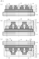
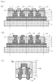
- FIG. 1 to 6 are views for explaining a method of manufacturing the semiconductor device 30 according to the first embodiment of the present invention.
- FIG. 1 to FIG. 5 are cross-sectional views illustrating a process of forming an intermediate laminate 29 including the wiring layer 16, the semiconductor chip 23, the sealing layer 24, and the like on the support substrate 11, and
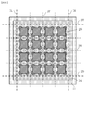
- FIG. 4 is a top view showing a state in which a plurality of intermediate laminated bodies 29 are formed in parallel on the support substrate 11.
- FIG. 6 illustration of some members, such as the sealing layer 24 mentioned later, is abbreviate
- the support substrate 11 is substantially square and one side is about 100 to 300 mm.
- a plurality of intermediate laminated bodies 29 including a sealing layer, a semiconductor chip, and a wiring layer described later are formed in parallel on the support substrate 11. Thereafter, the peripheral portion of the support substrate 11 is cut at the positions of the left end cutting line 2L, the right end cutting line 2R, the upper end cutting line 2U, and the lower end cutting line 2D indicated by broken lines in FIG.
- the left end cutting line 2L, the right end cutting line 2R, the upper end cutting line 2U, and the lower end cutting line 2D are collectively referred to as a cutting line 2.
- a plurality of intermediate laminated bodies 29 formed in parallel are peeled from the support substrate 11 at once. Thereafter, each of the plurality of intermediate stacked bodies 29 arranged in parallel is separated (diced) at the positions of a plurality of vertical separation lines 3V and a plurality of horizontal separation lines 3H indicated by broken lines in FIG.
- the vertical separation line 3V and the horizontal separation line 3H are collectively referred to as a separation line 3.
- the intermediate laminated body 29 is completed as the semiconductor device 30 through subsequent steps described later.
- the position of the cutting line 2 and the interval between the separation lines 3 are set according to the size (area) of the semiconductor device 30.
- FIG. 1A is a diagram showing a cross-sectional structure of the support substrate 11 in the initial stage of the manufacturing process.
- the structure of the support substrate 11 is the same structure as the copper foil with a carrier disclosed in Japanese Patent No. 6203388.
- the support substrate 11 itself is made of glass, and on its main surface (the surface on the front side, the upper surface in the figure), an adhesion metal layer 12, a release layer 13, and an antireflection layer in that order from the substrate side. 14 and a thin copper layer 15 are formed.
- the material and thickness constituting each of the above layers may be the same as the copper foil with carrier disclosed in Japanese Patent No. 6203388.
- the support substrate 11 itself is made of glass, and the thickness is preferably 100 to 2000 ⁇ m.
- the adhesion metal layer 12 is preferably a layer composed of at least one metal selected from the group consisting of Ti, Cr, and Ni from the viewpoint of ensuring adhesion with the support substrate 11 and is a pure metal. It may be an alloy or an alloy.
- the thickness of the adhesion metal layer 12 is preferably about 10 to 300 nm.
- the release layer 13 is preferably a layer mainly containing carbon from the viewpoint of ease of peeling, film formation, and the like, more preferably a layer mainly made of carbon or hydrocarbon, more preferably a hard carbon film. It consists of some amorphous carbon.
- the thickness of the release layer 13 is preferably about 1 to 20 nm.
- the antireflection layer 14 is made of at least one metal selected from the group consisting of Cr, W, Ta, Ti, Ni, and Mo.
- the thickness of the antireflection layer 14 is preferably about 10 to 300 nm.
- the antireflection layer 14 is a layer provided to improve the accuracy of the image inspection of the wiring layer in the manufacturing process, and may be omitted when the inspection process using an image is not necessary.
- the thin copper layer 15 is a layer mainly composed of copper having a thickness of about 50 to 2000 nm.
- the thin copper layer 15 is preferably formed by vacuum deposition, sputtering or plating.
- the adhesion metal layer 12, the release layer 13, and the antireflection layer 14 are also preferably formed by sputtering or the like. Moreover, if the support substrate 11 formed with the release layer 13 and the like suitable for the above conditions is sold, it may be purchased, that is, prepared and used.
- FIG. 1B shows a state in which a lower pad 16 that is a part of the semiconductor device 30 is formed on the thin copper layer 15 that is the uppermost layer on the support substrate 11.
- a photoresist layer (not shown) is first formed on the entire surface of the thin copper layer 15, and a desired pattern corresponding to the shape of the lower pad 16 is formed on the photoresist layer.
- FIG. 1B shows a state in which the photoresist is removed after the lower pad 16 is formed.
- the thickness of the lower pad 16 is preferably about 5 to 200 ⁇ m, and the diameter of the lower pad 16 is preferably about 30 to 200 ⁇ m.
- the upper surface shape of the lower pad 16 may be circular or polygonal.
- the surface and side surfaces of the lower pad 16 are roughened or a coupling agent is formed to improve the adhesion between the two. It may be improved. Further, based on the above-described steps, wiring for electrically connecting two different locations on the support substrate 11 simultaneously with the lower pad 16 can be formed according to the shape of the pattern formed on the photoresist.
- FIG. 1C shows a state in which an interlayer insulating film 17 is formed on the support substrate 11 so as to cover the lower pad 16 and a dry film resist 19 is formed thereon.
- an epoxy resin containing 80% or more of silicon filler is used as a material of the interlayer insulating film 17.
- the interlayer insulating film 17 is formed by a printing method, a compression molding method, or a method of vacuum laminating a sheet-like resin film, and a certain degree of curing is performed after the formation.
- a through hole 18 for forming a via is formed in a predetermined portion of the interlayer insulating film 17 by ablation by laser irradiation or the like, and a residue due to the formation of the through hole Desmear treatment to remove.
- a plating seed layer (not shown) made of a metal such as copper is formed on the interlayer insulating film 17 in which the through holes 18 are formed by electroless plating or sputtering.
- a dry film resist 19 is formed thereon, and an opening 20 is formed at a predetermined location in the dry film resist 19 that partially overlaps the through hole 18 by ablation by laser irradiation or the like.
- FIG. 1C shows a state in which the opening 20 is formed.
- a feeding electrode is attached to the plating seed layer (not shown) formed on the interlayer insulating film 17 on the support substrate 11 outside the cutting line 2. Then, by immersing the support substrate 11 in a plating solution and performing electrolytic plating such as copper plating, a metal such as copper is deposited inside the through hole 18 and the opening 20, thereby forming a via and an upper pad 21 (hereinafter, collectively) (Referred to as upper pad 21).
- FIG. 2A shows a state in which the upper pad 21 is formed inside the through hole 18 and the opening 20. Since both the lower pad 16 and the upper pad 21 are conductive members, they can also be called wiring layers.
- the dry film resist 19 is removed, and the interlayer insulating film 17 is cured. Further, the plating seed layer (not shown) formed on the interlayer insulating film 17 is removed (etched). These removals may be performed by a known general method.
- FIG. 2B shows a case where the semiconductor chip 23 is bonded onto the laminate (the lower pad 16, the upper pad 21, and the interlayer insulating film 17) formed on the support substrate 11 and the semiconductor chip 23 is sealed.
- 24 represents a sealed state.
- the bonding between the copper pillar 22 and the upper pad 21 may be performed by ultrasonic bonding.
- solder ball bumps or micro solder bumps may be formed on the semiconductor chip 23 instead of the soldered copper pillars 22.
- a sealing layer 24 made of resin is formed by a compression molding method or the like so as to cover the main surface of the semiconductor chip 23 and the support substrate 11 (the upper surface in FIG. 2B).
- the sealing layer 24 also covers the upper surface and side surfaces of the lower pad 16, the upper pad 21 and the interlayer insulating film 17, and the release layer 13 formed on the support substrate 11 or the antireflection layer 14 above the release layer 13 is also formed. cover.
- an intermediate laminate 29 including the sealing layer 24, the semiconductor chip 23, the copper pillar 22, the wiring layer (upper pad 21 and lower pad 16), and the interlayer insulating film 17 is formed on the support substrate 11.
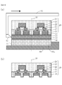
- FIG. 2C shows the support substrate 11 arranged with the main surface on which the intermediate laminated body 29 is formed facing downward for cutting the peripheral portion. 2B and 2C, since the support substrate 11 is rotated 180 degrees around a line perpendicular to the paper surface, the positional relationship between the right end cutting line 2R and the left end cutting line 2L is switched. ing.
- the scribing wheel 70 causes a minute scratch on the portion corresponding to the right end cutting line 2R and the left end cutting line 2L on the back surface (the surface opposite to the main surface) of the support substrate 11. Cut lines 4R, 4L are formed. Similarly, a cut line is also formed in a portion corresponding to the upper end cutting line 2U and the lower end cutting line 2D on the back surface of the support substrate 11.
- FIG. 3A shows the support substrate 11 arranged by rotating the upper and lower sides after cutting the peripheral portion.
- the laminate such as the sealing layer 24 on the main surface side of the support substrate 11 is cut by using a dicing saw 71 at portions corresponding to the left end cutting line 2L and the right end cutting line 2R.
- the laminate such as the sealing layer 24 on the main surface side of the support substrate 11 is cut.
- the dicing saw 71 cuts the sealing layer 24, the interlayer insulating film 17, the antireflection layer 14, the release layer 13, and the adhesion metal layer 12, but a cut is partially formed in the vicinity of the main surface of the support substrate 11. It doesn't matter. Since the cut laminate is in close contact with the main surface of the peripheral portion of the support substrate 11 (outside the cutting line 2), even if the peripheral portion of the support substrate 11 is connected to the support substrate 11, it may be cut. It does not leave the support substrate 11 immediately. The support substrate 11 is cleaved (breaked) at the position of the cutting line 2 by applying a striking force to the peripheral portion (outer peripheral portion than the cutting line 2) of the supporting substrate 11 in this state.
- FIG. 3B shows the support substrate 11 and the intermediate laminate 29 in a state where the peripheral portion is cleaved. As shown in FIG. 3B, the end of the release layer 13 is clearly exposed on the cut surface of the intermediate laminate 29.
- the cut lines 4R and 4L are cracks formed to perform this cleaving (break), and thus can be regarded as a cleaving planned line.
- FIG. 4A shows a state in which the support substrate 11 and the intermediate laminate 29 with the peripheral portion cut are mounted on the peeling device (80, 81), and the intermediate laminate 29 is peeled from the support substrate 11.
- the peeling apparatus is an apparatus including a mounting table 80 on which the support substrate 11 is placed and a peeling arm 81 provided with a crack initiator 82 such as a needle.
- the intermediate laminate 29 In the peeling of the intermediate laminate 29, first, one end (the right end in FIG. 4B) of the support substrate 11 is fixed to the locking portion 80a on the mounting table 80. Then, the tip of the crack initiator 82 is brought into contact with the vicinity of the release layer 13 formed on the support substrate 11 and is pushed onto the support substrate 11 to form a release start point. And the intermediate
- the intermediate laminate 29 can be uniformly released from the support substrate 11 with the release layer 13 as a boundary surface. Subsequently, the debris of the release layer 13, the antireflection layer 14, and the thin copper layer 15 remaining on the release surface are removed from the intermediate laminate 29 peeled from the support substrate 11.
- FIG. 4B shows an intermediate laminate 29 which is peeled off from the support substrate 11 and from which the debris of the peeling layer 13, the antireflection layer 14 and the thin copper layer 15 are removed.
- a known general removal method such as etching can also be used for removing the debris of the release layer 13, the antireflection layer 14, and the thin copper layer 15.
- FIG. 5A shows that a solder resist 25 is formed on the interlayer insulating film 17 in order to form solder balls on the lower pad 16 of the intermediate laminate 29, and an opening 27 is formed in the solder resist 25 on the lower pad 16.
- the state in which is formed is shown.
- the intermediate laminate 29 is shown rotated (inverted upside down) from the state shown in FIG. 4B. Thereafter, flux is applied onto the opening 27 of the solder resist 25, the solder balls 26 are temporarily fixed on the lower pads 16, and then reflow is performed to fix the solder balls 26.
- FIG. 5B shows the intermediate laminate 29 in a state where the solder balls 26 are fixed.
- each of the intermediate laminates 29 in parallel is tested with a circuit tester or the like and diced (divided into pieces) using a dicing saw.
- FIG. 5C shows the semiconductor device 30 in a completed state after dicing.
- the length in the thickness direction is shown enlarged with respect to the length in the in-plane direction of the support substrate 11 for ease of explanation.
- two intermediate laminates 29 are formed on the support substrate 11 on the left and right.
- the number of the intermediate laminates 29 formed on the support substrate 11 is the number of arrangements. However, the number of intermediate laminated bodies 29 can be increased.
- the solder ball forming step described above may be omitted.
- Modifications 1 to 4 will be described with reference to FIG.
- the following modification is a modification regarding the cutting method of the support substrate 11. Therefore, since the method other than the cutting method of the support substrate 11 is the same as that of the first embodiment described above, the description thereof is omitted.
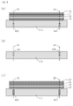
- FIG. 7A shows a support substrate 11a used in the first modification. Similar to the support substrate 11 used in the first embodiment described above, the support substrate 11a has an adhesion metal layer 12, a release layer 13, an antireflection layer 14, and thin copper on the main surface in order from the substrate side. Layer 15 is formed. However, incisions 4aL and 4aR are formed in advance on the back surface (surface opposite to the main surface) at positions corresponding to the cutting line 2 such as the left end cutting line 2L and the right end cutting line 2R. .
- the first modification it is possible to reduce a step (for example, see FIG. 3C) of forming a cut line on the back surface of the support substrate 11a in the manufacturing process of the semiconductor device.
- the cut lines 4aL and 4aR, the adhesion metal layer 12, the release layer 13, the antireflection layer 14 and the thin copper layer 15 may be formed first.
- the cut lines 4aL and 4aR are preferably performed before the wiring layer (lower pad 16) is formed on the support substrate 11a.
- the cut lines 4aL and 4aR of the first modification can also be considered as planned cutting lines, similar to the cut lines 4L and 4R in the first embodiment described above.
- FIG. 7B shows a support substrate 11b used in the second modification.
- the cut lines 4bL and 4bR are formed in advance at positions corresponding to the cutting lines 2 such as the left end cutting line 2L and the right end cutting line 2R on the main surface of the support substrate 11b.
- an adhesion metal layer 12, a release layer 13, an antireflection layer 14, and a thin copper layer 15 are formed on the main surface in this order from the substrate side.
- the cut line formed on the main surface of the support substrate 11b it functions as a starting point of the break (break) in the same manner as the cut line formed on the back surface. Among them, it is possible to reduce the step of forming the cut line on the back surface of the support substrate 11b.
- the cut lines 4bL and 4bR of Modification 2 can also be regarded as planned cutting lines, similar to the cut lines 4L and 4R in the first embodiment described above.
- FIG. 7C shows a support substrate 11 c used in the third modification. Similar to the support substrate 11 used in the first embodiment described above, the support substrate 11c has an adhesion metal layer 12, a release layer 13, an antireflection layer 14, and a thin copper layer on the main surface in order from the substrate side. 15 is formed. Deteriorated portions 4cL and 4cR that are weaker than other portions are formed in positions corresponding to the cutting lines 2 such as the left end cutting line 2L and the right end cutting line 2R inside the support substrate 11c. .
- the deteriorated portions 4cL and 4cR can be formed by, for example, condensing and irradiating a laser on the deteriorated portion of the glass support substrate 11c. Since the deteriorated portions 4cL and 4cR function as a starting point of breakage (break), even in the third modification, it is possible to reduce the step of forming a cut line on the back surface of the support substrate 11c in the manufacturing process of the semiconductor device. .
- the deteriorated portions 4cL and 4cR of the third modification can also be regarded as the planned cutting lines, similar to the cut lines 4L and 4R in the first embodiment described above.
- Modification 4 In the fourth modification, when the peripheral portion of the support substrate 11 is cut, the entire support substrate 11 is cut using a dicing saw, instead of cutting the support substrate 11 with a cut line. Therefore, in the modified example 4, compared to the first embodiment and each modified example described above, the cutting process (for example, see FIG. 2C) and the cleaving process can be reduced. Simplified.
- the support substrate 11 having the release layer 13 formed on the main surface side is prepared, partially above the release layer 13 on the support substrate 11.
- Forming a wiring layer (lower pad 16, upper pad 21) disposing the semiconductor chip 23 on the support substrate 11, including at least part of the wiring layer (lower pad 16, upper pad 21) and the semiconductor chip 23.
- a sealing layer 24 in contact with the release layer 13 on the support substrate 11 or a layer above it is formed, and the semiconductor chip 23, the wiring layers 16, 21, and the sealing layer 24 are formed on the support substrate 11.
- Mechanically peeled to be a includes a city. Since such a manufacturing method is adopted, even if film formation unevenness or scratches due to contact with the electrolytic plating electrode occur in the peripheral portion of the support substrate 11, those adverse effects do not reach the center portion of the support substrate 11, The laminated body 29 can be stably peeled from the support substrate 11. As a result, the yield of the intermediate stacked body 29 and the semiconductor device including the intermediate stacked body can be improved.
- cutting of the peripheral portion of the support substrate 11 is planned to form a cutting line in the peripheral portion of the support substrate 11, and the peeling layer 13 and the sealing layer 24 formed on the support substrate 11 are scheduled to be cut.
- the periphery of the support substrate 11 can be stabilized more stably. Therefore, the yield can be further improved.
- the support substrate 11 by using a support substrate in which the metal layer 12, the release layer 13, and the thin copper layer 14 are formed in this order from the substrate side, the release from the release layer 13 is further improved. It can be realized stably.
- a plurality of intermediate laminated bodies 29 are formed in parallel on the support substrate 11, and the plurality of intermediate laminated bodies 29 formed in parallel are peeled integrally from the support substrate 11, and after peeling.
- FIG. 8 a second embodiment of the method for manufacturing the semiconductor device 30a will be described.
- the number of wiring layers to be formed is three.
- the manufacturing process in the second embodiment is the same as that in the first embodiment.
- a second interlayer insulating film 31 is formed on the upper pad 21 and the interlayer insulating film 17, and a through hole 32 is formed in a predetermined portion of the second interlayer insulating film 31.
- a plating seed layer (not shown) made of a metal such as copper is formed on the second interlayer insulating film 31 after the formation of the through hole 32 by electroless plating or sputtering. Then, a dry film resist 33 is formed thereon, and an opening 34 is formed at a predetermined location in the dry film resist 33.
- FIG. 7A shows a state in which the opening 34 is formed.
- electrolytic plating such as copper plating is performed to deposit a metal such as copper inside the through hole 32 and the opening 34, thereby forming the uppermost pad 35. Since the uppermost pad 35 is also a conductive member, it can be regarded as a part of the wiring layer.
- the dry film resist 33 is removed, and the second interlayer insulating film 31 is cured. Further, the plating seed layer (not shown) formed on the second interlayer insulating film 31 is removed (etched).
- FIG. 7B shows a state where the uppermost pad 35 is formed and the dry film resist 33 is removed.
- the semiconductor device 30a which is the pad 16, the upper pad 21, and the uppermost pad 35
- a semiconductor device having four or more wiring layers can be manufactured by further adding the same process as the process added in the second embodiment to the first embodiment described above in the second embodiment. It is.
- the support substrate 11 itself is made of glass.
- the support substrate 11 itself may be a substrate made of any one of ceramics, resin, or metal.
- the shape of the support substrate 11 is not limited to a square, and may be other shapes such as a rectangle or a circle.
- the lower pad 16, the upper pad 21, and the uppermost pad 35 are not limited to copper, and may be formed of other metals.
- Various types of photoresists may be photosensitive dry films, and pattern formation may be performed by laser ablation.
- each intermediate laminate 29 is not limited to one, and a plurality of semiconductor chips 23 may be arranged in one intermediate laminate 29. Thereby, the higher performance intermediate laminate 29 and the semiconductor device 30 can be realized.
- the electronic component disposed in each intermediate laminate 29 is not limited to the semiconductor chip 23, and passive components such as a capacitor, a coil, and an antenna may be disposed together with the semiconductor chip 23. As a result, it is possible to realize a high-functional intermediate laminate 29 and a semiconductor device 30 having functions that cannot be realized only by the semiconductor chip 23.
- the present invention is not limited to the above contents. Other embodiments conceivable within the scope of the technical idea of the present invention are also included in the scope of the present invention.
Landscapes
- Engineering & Computer Science (AREA)
- Microelectronics & Electronic Packaging (AREA)
- Power Engineering (AREA)
- Computer Hardware Design (AREA)
- General Physics & Mathematics (AREA)
- Condensed Matter Physics & Semiconductors (AREA)
- Physics & Mathematics (AREA)
- Manufacturing & Machinery (AREA)
- Internal Circuitry In Semiconductor Integrated Circuit Devices (AREA)
- Production Of Multi-Layered Print Wiring Board (AREA)
- Bipolar Transistors (AREA)
- Crystals, And After-Treatments Of Crystals (AREA)
- Dicing (AREA)
Abstract
This method for manufacturing a semiconductor device includes: preparing a supporting substrate having a peeling layer that is formed on the main surface side; forming a wiring layer on a part of a region above the peeling layer on the supporting substrate; disposing a semiconductor chip on the supporting substrate so that a pad of the semiconductor chip is electrically connected to the wiring layer; forming a sealing layer, which includes the wiring layer and the semiconductor chip, and which is in contact with the peeling layer on the supporting substrate or a layer above the peeling layer, and forming, on the supporting substrate, an intermediate laminated body that includes the semiconductor chip, the wiring layer, and the sealing layer; cutting off a peripheral portion of the supporting substrate after forming the intermediate laminated body; and mechanically peeling, by having the peeling layer as a boundary, the intermediate laminated body from the supporting substrate from which the peripheral portion has been cut off.
Description
本発明は、半導体装置の製造方法に関する。
The present invention relates to a method for manufacturing a semiconductor device.
いわゆるチップラスト型(RDLファースト型)の半導体装置は、一時的に使用する仮の支持基板上に配線層および絶縁層を形成し、半導体チップを配置してモールドした後、仮の支持基板を除去する工程を経て製造される。仮の支持基板の除去は、モールドされた半導体チップ、配線層および絶縁層(以下、これらを総称して中間積層体とよぶ)から、仮の支持基板を機械的に引き剥がして分離することにより行われる。
特許文献1には、表面上に密着金属層、剥離層、反射防止層および極薄銅層を備えたガラスで構成されるキャリア(支持基板)を用いるプリント配線板(半導体装置)の製造方法が開示される。 A so-called chip last type (RDL first type) semiconductor device is formed by forming a wiring layer and an insulating layer on a temporary support substrate that is temporarily used, placing and molding the semiconductor chip, and then removing the temporary support substrate. It is manufactured through the process of. The temporary support substrate is removed by mechanically peeling and separating the temporary support substrate from the molded semiconductor chip, wiring layer, and insulating layer (hereinafter collectively referred to as an intermediate laminate). Done.
Patent Document 1 discloses a method of manufacturing a printed wiring board (semiconductor device) using a carrier (support substrate) made of glass having a close-contact metal layer, a release layer, an antireflection layer, and an ultrathin copper layer on the surface. Disclosed.
特許文献1は、支持基板(キャリア)上に形成した中間積層体を、支持基板の全面に渡って一括して支持基板から剥離する方法を開示する。
しかし、支持基板の周辺部は、成膜条件が不安定なため配線層や絶縁層を安定した膜厚で成膜することが難しく、また、周辺部には配線層の形成のための電気めっき工程において給電機構(給電用電極)を接触させる必要があり、これによりキズ等が発生し易い。 Patent Document 1 discloses a method of peeling an intermediate laminate formed on a support substrate (carrier) all at once from the support substrate over the entire surface of the support substrate.
However, it is difficult to form a wiring layer or an insulating layer with a stable film thickness on the periphery of the support substrate because the film formation conditions are unstable, and electroplating for forming a wiring layer on the periphery is difficult. In the process, the power feeding mechanism (power feeding electrode) needs to be brought into contact with each other.
そのため、支持基板上の周辺部も含めて剥離を行うと、配線層および絶縁層の不均一性やキズが原因で、周辺部に剥離ムラが発生する恐れがある。そして、周辺部の剥離ムラが、半導体チップと配線層がモールドされた中間積層体が形成されている基板の中央部分の剥離にも悪影響を与え、中間積層体およびその中間積層体を含む半導体装置の歩留まりを低下させる恐れがある。
Therefore, if peeling is performed including the peripheral portion on the support substrate, uneven peeling may occur in the peripheral portion due to non-uniformity and scratches on the wiring layer and the insulating layer. Further, the peeling unevenness in the peripheral part adversely affects the peeling of the central portion of the substrate on which the intermediate laminate in which the semiconductor chip and the wiring layer are molded is formed, and the intermediate laminate and the semiconductor device including the intermediate laminate There is a risk of lowering the yield.
(1)本発明の第1の態様による半導体装置の製造方法は、主面側に剥離層が形成された支持基板を用意すること、前記支持基板上の前記剥離層よりも上に、部分的に配線層を形成すること、半導体チップのパッドの少なくとも一部が、前記配線層の少なくとも一部に電気的に接続するように、前記半導体チップを前記支持基板上に配置すること、前記配線層の少なくとも一部および前記半導体チップを包含するとともに、前記支持基板上の前記剥離層またはそれよりも上の層と接触する封止層を形成し、前記支持基板上に、前記半導体チップおよび前記配線層、前記封止層を含む中間積層体を形成すること、前記中間積層体を形成した後に、前記支持基板の周辺部を切断すること、および、前記周辺部を切断した前記支持基板から、前記剥離層を境界として、前記中間積層体を機械的に剥離すること、とを含む。
(2)本発明の第2の態様による半導体装置の製造方法は、第1の態様に記載の半導体装置の製造方法において、前記支持基板の前記周辺部の前記切断は、前記支持基板の周辺部に、割断予定線を形成すること、前記支持基板上に形成されている前記剥離層および前記封止層を、前記割断予定線に対応する位置で前記支持基板の主面側から切断すること、前記支持基板の周辺部を、前記割断予定線に沿って割断すること、とを含むことが好ましい。
(3)本発明の第3の態様による半導体装置の製造方法は、第2の態様に記載の半導体装置の製造方法において、前記割断予定線の形成は、前記支持基板の裏面に切り筋を形成することにより行うことが好ましい。
(4)本発明の第4の態様による半導体装置の製造方法は、第3の態様に記載の半導体装置の製造方法において、前記切り筋の形成は、前記支持基板上に前記中間積層体を形成した後に行うことが好ましい。
(5)本発明の第5の態様による半導体装置の製造方法は、第3の態様に記載の半導体装置の製造方法において、前記切り筋の形成は、前記支持基板上に前記配線層を形成する前に行うことが好ましい。
(6)本発明の第6の態様による半導体装置の製造方法は、第2の態様に記載の半導体装置の製造方法において、前記割断予定線の形成は、前記剥離層を形成する前に、前記支持基板の主面に切り筋を形成することにより行うことが好ましい。
(7)本発明の第7の態様による半導体装置の製造方法は、第2の態様に記載の半導体装置の製造方法において、前記割断予定線の形成は、前記支持基板の内部に、他の部分と比較して強度の弱い部分を形成することにより行うことが好ましい。
(8)本発明の第8の態様による半導体装置の製造方法は、第1から第7までのいずれか1つの態様に記載の半導体装置の製造方法において、前記支持基板として、前記主面に基板側から順に金属層、前記剥離層、薄銅層が形成されている支持基板を用いることが好ましい。
(9)本発明の第9の態様による半導体装置の製造方法は、第1から第7までのいずれか1つの態様に記載の半導体装置の製造方法において、前記配線層の形成を複数回行い、多層配線型の配線層を形成することが好ましい。
(10)本発明の第10の態様による半導体装置の製造方法は、第1から第7までのいずれか1つの態様に記載の半導体装置の製造方法において、前記支持基板上に、複数並列して前記中間積層体を形成し、かつ、前記複数並列して形成された前記中間積層体を一体的に前記支持基板から剥離するとともに、前記剥離後に前記中間積層体を個々に切断することが好ましい。
(11)本発明の第11の態様による半導体装置の製造方法は、第1から第7までのいずれか1つの態様に記載の半導体装置の製造方法において、前記中間積層体中に前記半導体チップを複数個配置することが好ましい。
(12)本発明の第12の態様による半導体装置の製造方法は、第1から第7までのいずれか1つの態様に記載の半導体装置の製造方法において、前記中間積層体中に前記半導体チップとともに受動部品を配置することが好ましい。 (1) A method of manufacturing a semiconductor device according to the first aspect of the present invention includes preparing a support substrate having a release layer formed on the main surface side, partially above the release layer on the support substrate. Forming a wiring layer on the semiconductor substrate, disposing the semiconductor chip on the support substrate so that at least a part of a pad of the semiconductor chip is electrically connected to at least a part of the wiring layer, the wiring layer And forming a sealing layer in contact with the release layer on the support substrate or a layer above the support layer, and the semiconductor chip and the wiring on the support substrate Forming a layer, an intermediate laminate including the sealing layer, cutting the peripheral portion of the support substrate after forming the intermediate laminate, and from the support substrate cutting the peripheral portion, Peeling The layers as a boundary, mechanically peeled to be the intermediate laminate, including capital.
(2) A method for manufacturing a semiconductor device according to a second aspect of the present invention is the method for manufacturing a semiconductor device according to the first aspect, wherein the cutting of the peripheral portion of the support substrate is performed at the peripheral portion of the support substrate. Forming a planned cutting line, cutting the release layer and the sealing layer formed on the support substrate from a main surface side of the support substrate at a position corresponding to the planned cutting line, It is preferable to include cutting the peripheral portion of the support substrate along the planned cutting line.
(3) A method for manufacturing a semiconductor device according to a third aspect of the present invention is the method for manufacturing a semiconductor device according to the second aspect, wherein the cut line is formed by forming a score on the back surface of the support substrate. It is preferable to carry out by doing.
(4) A method for manufacturing a semiconductor device according to a fourth aspect of the present invention is the method for manufacturing a semiconductor device according to the third aspect, wherein the cut line is formed by forming the intermediate laminate on the support substrate. It is preferable to carry out after.
(5) A method for manufacturing a semiconductor device according to a fifth aspect of the present invention is the method for manufacturing a semiconductor device according to the third aspect, wherein the cut line is formed by forming the wiring layer on the support substrate. Preferably it is done before.
(6) A method for manufacturing a semiconductor device according to a sixth aspect of the present invention is the method for manufacturing a semiconductor device according to the second aspect, wherein the dividing line is formed before the release layer is formed. This is preferably performed by forming a cut line on the main surface of the support substrate.
(7) A method for manufacturing a semiconductor device according to a seventh aspect of the present invention is the method for manufacturing a semiconductor device according to the second aspect, wherein the splitting line is formed in the support substrate at another portion. It is preferable to carry out by forming a weak part compared with.
(8) A method for manufacturing a semiconductor device according to an eighth aspect of the present invention is the method for manufacturing a semiconductor device according to any one of the first to seventh aspects, wherein the substrate is formed on the main surface as the support substrate. It is preferable to use a support substrate on which a metal layer, the release layer, and a thin copper layer are formed in this order from the side.
(9) A method for manufacturing a semiconductor device according to a ninth aspect of the present invention is the method for manufacturing a semiconductor device according to any one of the first to seventh aspects, wherein the wiring layer is formed a plurality of times, It is preferable to form a multilayer wiring type wiring layer.
(10) A method for manufacturing a semiconductor device according to a tenth aspect of the present invention is the method for manufacturing a semiconductor device according to any one of the first to seventh aspects, wherein a plurality of semiconductor devices are arranged in parallel on the support substrate. Preferably, the intermediate laminate is formed, and the plurality of the intermediate laminates formed in parallel are integrally peeled from the support substrate, and the intermediate laminate is individually cut after the peeling.
(11) A method for manufacturing a semiconductor device according to an eleventh aspect of the present invention is the method for manufacturing a semiconductor device according to any one of the first to seventh aspects, wherein the semiconductor chip is placed in the intermediate laminate. It is preferable to arrange a plurality.
(12) A method for manufacturing a semiconductor device according to a twelfth aspect of the present invention is the method for manufacturing a semiconductor device according to any one of the first to seventh aspects, together with the semiconductor chip in the intermediate laminate. It is preferable to arrange passive components.
本発明によれば、支持基板の周辺部に形成された膜の不均一性やキズによらず、中間積層体を安定して剥離することができる。
According to the present invention, the intermediate laminate can be stably peeled regardless of the nonuniformity and scratches of the film formed on the periphery of the support substrate.
(第1の実施形態)
図1から図6は、本発明の第1の実施形態による半導体装置30の製造方法を説明するための図である。図1から図5は、支持基板11上に、配線層16、半導体チップ23、封止層24等からなる中間積層体29を形成していく工程等を説明する断面図であり、図6は、支持基板11上に中間積層体29が複数並列して形成された状態を示す上面図である。ただし、図6では後述する封止層24等の一部の部材は図示を省略している。 (First embodiment)
1 to 6 are views for explaining a method of manufacturing thesemiconductor device 30 according to the first embodiment of the present invention. FIG. 1 to FIG. 5 are cross-sectional views illustrating a process of forming an intermediate laminate 29 including the wiring layer 16, the semiconductor chip 23, the sealing layer 24, and the like on the support substrate 11, and FIG. 4 is a top view showing a state in which a plurality of intermediate laminated bodies 29 are formed in parallel on the support substrate 11. FIG. However, in FIG. 6, illustration of some members, such as the sealing layer 24 mentioned later, is abbreviate | omitted.
図1から図6は、本発明の第1の実施形態による半導体装置30の製造方法を説明するための図である。図1から図5は、支持基板11上に、配線層16、半導体チップ23、封止層24等からなる中間積層体29を形成していく工程等を説明する断面図であり、図6は、支持基板11上に中間積層体29が複数並列して形成された状態を示す上面図である。ただし、図6では後述する封止層24等の一部の部材は図示を省略している。 (First embodiment)
1 to 6 are views for explaining a method of manufacturing the
(製造工程の概要)
図6を参照して、本例の製造工程の概要を説明する。
図6に示すように、本例では、支持基板11は略正方形で、一辺が100~300mm程度である。そして、本例においては、図6に示すとおり、この支持基板11上に、後述する封止層や半導体チップおよび配線層を含む中間積層体29を複数並列して形成する。
その後、図6中に破線で示した左端切断線2L、右端切断線2R、上端切断線2U、下端切断線2Dの位置にて、支持基板11の周辺部を切断する。左端切断線2L、右端切断線2R、上端切断線2Uおよび下端切断線2Dを、総称して切断線2と呼ぶ。 (Outline of manufacturing process)
With reference to FIG. 6, the outline | summary of the manufacturing process of this example is demonstrated.
As shown in FIG. 6, in this example, thesupport substrate 11 is substantially square and one side is about 100 to 300 mm. In this example, as shown in FIG. 6, a plurality of intermediate laminated bodies 29 including a sealing layer, a semiconductor chip, and a wiring layer described later are formed in parallel on the support substrate 11.
Thereafter, the peripheral portion of thesupport substrate 11 is cut at the positions of the left end cutting line 2L, the right end cutting line 2R, the upper end cutting line 2U, and the lower end cutting line 2D indicated by broken lines in FIG. The left end cutting line 2L, the right end cutting line 2R, the upper end cutting line 2U, and the lower end cutting line 2D are collectively referred to as a cutting line 2.
図6を参照して、本例の製造工程の概要を説明する。
図6に示すように、本例では、支持基板11は略正方形で、一辺が100~300mm程度である。そして、本例においては、図6に示すとおり、この支持基板11上に、後述する封止層や半導体チップおよび配線層を含む中間積層体29を複数並列して形成する。
その後、図6中に破線で示した左端切断線2L、右端切断線2R、上端切断線2U、下端切断線2Dの位置にて、支持基板11の周辺部を切断する。左端切断線2L、右端切断線2R、上端切断線2Uおよび下端切断線2Dを、総称して切断線2と呼ぶ。 (Outline of manufacturing process)
With reference to FIG. 6, the outline | summary of the manufacturing process of this example is demonstrated.
As shown in FIG. 6, in this example, the
Thereafter, the peripheral portion of the
周辺部を切断した後に、支持基板11から、複数並列して形成された中間積層体29を一括して剥離する。その後、複数並列された中間積層体29のそれぞれを、図6中に破線で示した複数の縦分離線3V、複数の横分離線3Hの位置にて分離(ダイシング)する。縦分離線3Vおよび横分離線3Hを、総称して分離線3と呼ぶ。
中間積層体29は、後述するその後の工程を経て、半導体装置30として完成される。 切断線2の位置および分離線3の間隔は、半導体装置30の大きさ(面積)に応じて設定される。
以下、図1から図5を参照して、支持基板11上に、配線層16、半導体チップ23、封止層24等からなる中間積層体29を形成する工程、および半導体装置30を形成する
工程を説明する。 After cutting the peripheral portion, a plurality of intermediatelaminated bodies 29 formed in parallel are peeled from the support substrate 11 at once. Thereafter, each of the plurality of intermediate stacked bodies 29 arranged in parallel is separated (diced) at the positions of a plurality of vertical separation lines 3V and a plurality of horizontal separation lines 3H indicated by broken lines in FIG. The vertical separation line 3V and the horizontal separation line 3H are collectively referred to as a separation line 3.
The intermediatelaminated body 29 is completed as the semiconductor device 30 through subsequent steps described later. The position of the cutting line 2 and the interval between the separation lines 3 are set according to the size (area) of the semiconductor device 30.
Hereinafter, with reference to FIG. 1 to FIG. 5, a step of forming anintermediate laminate 29 composed of the wiring layer 16, the semiconductor chip 23, the sealing layer 24, and the like on the support substrate 11 and a step of forming the semiconductor device 30. Will be explained.
中間積層体29は、後述するその後の工程を経て、半導体装置30として完成される。 切断線2の位置および分離線3の間隔は、半導体装置30の大きさ(面積)に応じて設定される。
以下、図1から図5を参照して、支持基板11上に、配線層16、半導体チップ23、封止層24等からなる中間積層体29を形成する工程、および半導体装置30を形成する
工程を説明する。 After cutting the peripheral portion, a plurality of intermediate
The intermediate
Hereinafter, with reference to FIG. 1 to FIG. 5, a step of forming an
(支持基板)
図1(a)は、製造工程の初期おける支持基板11の断面構造を示す図である。支持基板11の構成は、日本国特許第6203988号公報に開示されるキャリア付き銅箔と同様の構成である。支持基板11自体はガラスからなり、その主面(おもて側の面であって、図中の上方の面)に、基板側から順に密着金属層12と、剥離層13と、反射防止層14と、薄銅層15が形成されている。上記の各層を構成する材料や厚さも、日本国特許第6203988号公報に開示されるキャリア付き銅箔と同様の構成でよい。 (Support substrate)
FIG. 1A is a diagram showing a cross-sectional structure of thesupport substrate 11 in the initial stage of the manufacturing process. The structure of the support substrate 11 is the same structure as the copper foil with a carrier disclosed in Japanese Patent No. 6203388. The support substrate 11 itself is made of glass, and on its main surface (the surface on the front side, the upper surface in the figure), an adhesion metal layer 12, a release layer 13, and an antireflection layer in that order from the substrate side. 14 and a thin copper layer 15 are formed. The material and thickness constituting each of the above layers may be the same as the copper foil with carrier disclosed in Japanese Patent No. 6203388.
図1(a)は、製造工程の初期おける支持基板11の断面構造を示す図である。支持基板11の構成は、日本国特許第6203988号公報に開示されるキャリア付き銅箔と同様の構成である。支持基板11自体はガラスからなり、その主面(おもて側の面であって、図中の上方の面)に、基板側から順に密着金属層12と、剥離層13と、反射防止層14と、薄銅層15が形成されている。上記の各層を構成する材料や厚さも、日本国特許第6203988号公報に開示されるキャリア付き銅箔と同様の構成でよい。 (Support substrate)
FIG. 1A is a diagram showing a cross-sectional structure of the
すなわち、支持基板11自体はガラスからなり、その厚さは100~2000μmが好ましい。
密着金属層12は支持基板11との密着性を確保する点から、Ti、Cr及びNiからなる群から選択される少なくとも1種の金属で構成される層であるのが好ましく、純金属であってもよいし、合金であってもよい。密着金属層12の厚さは、10~300nm程度が好ましい。
剥離層13は、主として炭素を含んでなる層であるのが剥離容易性や膜形成性の点等から好ましく、より好ましくは主として炭素又は炭化水素からなる層であり、さらに好ましくは硬質炭素膜であるアモルファスカーボンからなる。剥離層13の厚さは、1~20nm程度が好ましい。 That is, thesupport substrate 11 itself is made of glass, and the thickness is preferably 100 to 2000 μm.
Theadhesion metal layer 12 is preferably a layer composed of at least one metal selected from the group consisting of Ti, Cr, and Ni from the viewpoint of ensuring adhesion with the support substrate 11 and is a pure metal. It may be an alloy or an alloy. The thickness of the adhesion metal layer 12 is preferably about 10 to 300 nm.
Therelease layer 13 is preferably a layer mainly containing carbon from the viewpoint of ease of peeling, film formation, and the like, more preferably a layer mainly made of carbon or hydrocarbon, more preferably a hard carbon film. It consists of some amorphous carbon. The thickness of the release layer 13 is preferably about 1 to 20 nm.
密着金属層12は支持基板11との密着性を確保する点から、Ti、Cr及びNiからなる群から選択される少なくとも1種の金属で構成される層であるのが好ましく、純金属であってもよいし、合金であってもよい。密着金属層12の厚さは、10~300nm程度が好ましい。
剥離層13は、主として炭素を含んでなる層であるのが剥離容易性や膜形成性の点等から好ましく、より好ましくは主として炭素又は炭化水素からなる層であり、さらに好ましくは硬質炭素膜であるアモルファスカーボンからなる。剥離層13の厚さは、1~20nm程度が好ましい。 That is, the
The
The
反射防止層14は、Cr、W、Ta、Ti、Ni及びMoからなる群から選択される少なくとも1種の金属で構成される。反射防止層14の厚さは、10~300nm程度が好ましい。なお、反射防止層14は、製造工程での配線層の画像検査の精度を向上するために設ける層であるので、画像による検査工程が必要でない場合等には省略してもかまわない。
薄銅層15は、厚さが50~2000nm程度の銅を主成分とする層である。薄銅層15は、真空蒸着やスパッタリングまたはめっきにより形成することが好ましい。 Theantireflection layer 14 is made of at least one metal selected from the group consisting of Cr, W, Ta, Ti, Ni, and Mo. The thickness of the antireflection layer 14 is preferably about 10 to 300 nm. The antireflection layer 14 is a layer provided to improve the accuracy of the image inspection of the wiring layer in the manufacturing process, and may be omitted when the inspection process using an image is not necessary.
Thethin copper layer 15 is a layer mainly composed of copper having a thickness of about 50 to 2000 nm. The thin copper layer 15 is preferably formed by vacuum deposition, sputtering or plating.
薄銅層15は、厚さが50~2000nm程度の銅を主成分とする層である。薄銅層15は、真空蒸着やスパッタリングまたはめっきにより形成することが好ましい。 The
The
また、密着金属層12、剥離層13、反射防止層14についても、スパッタリング等で形成することが好ましい。
また、上記の条件に適した、剥離層13等の形成された支持基板11が販売されていれば、それを購入して、すなわち用意して、使用してもよい。 Theadhesion metal layer 12, the release layer 13, and the antireflection layer 14 are also preferably formed by sputtering or the like.
Moreover, if thesupport substrate 11 formed with the release layer 13 and the like suitable for the above conditions is sold, it may be purchased, that is, prepared and used.
また、上記の条件に適した、剥離層13等の形成された支持基板11が販売されていれば、それを購入して、すなわち用意して、使用してもよい。 The
Moreover, if the
(下段パッドの形成)
図1(b)は、支持基板11上の最上層である薄銅層15の上に、半導体装置30の一部となる下段パッド16を形成した状態を示している。下段パッド16の形成に際しては、始めに薄銅層15上の全面に不図示のフォトレジスト層を形成し、このフォトレジスト層に下段パッド16の形状に対応する所望のパターンを形成する。 (Formation of lower pad)
FIG. 1B shows a state in which alower pad 16 that is a part of the semiconductor device 30 is formed on the thin copper layer 15 that is the uppermost layer on the support substrate 11. When forming the lower pad 16, a photoresist layer (not shown) is first formed on the entire surface of the thin copper layer 15, and a desired pattern corresponding to the shape of the lower pad 16 is formed on the photoresist layer.
図1(b)は、支持基板11上の最上層である薄銅層15の上に、半導体装置30の一部となる下段パッド16を形成した状態を示している。下段パッド16の形成に際しては、始めに薄銅層15上の全面に不図示のフォトレジスト層を形成し、このフォトレジスト層に下段パッド16の形状に対応する所望のパターンを形成する。 (Formation of lower pad)
FIG. 1B shows a state in which a
その後、切断線2より外側の支持基板11上の薄銅層15に給電用電極を取り付け、支持基板11をめっき液に浸し銅めっき等の電解めっきを行うことで、薄銅層15が露出する部分(すなわちフォトレジストで覆われていない部分)に、下段パッド16を形成する。そして、フォトレジストを除去する。
図1(b)は、下段パッド16を形成した後にフォトレジストを除去した状態を示している。 Thereafter, the electrode for power feeding is attached to thethin copper layer 15 on the support substrate 11 outside the cutting line 2, and the support substrate 11 is immersed in a plating solution to perform electrolytic plating such as copper plating, thereby exposing the thin copper layer 15. The lower pad 16 is formed in the portion (that is, the portion not covered with the photoresist). Then, the photoresist is removed.
FIG. 1B shows a state in which the photoresist is removed after thelower pad 16 is formed.
図1(b)は、下段パッド16を形成した後にフォトレジストを除去した状態を示している。 Thereafter, the electrode for power feeding is attached to the
FIG. 1B shows a state in which the photoresist is removed after the
下段パッド16の厚さは5~200μm程度が好ましく、下段パッド16の直径は30~200μm程度が好ましい。下段パッド16の上面形状は、円形でも多角形でも良い。
下段パッド16と後述する層間絶縁膜17との密着性を向上するために、下段パッド16の表面および側面に粗面化処理を行うか、あるいはカップリング剤を形成して、両者の密着性を向上させてもよい。
また、上記の工程に基づいて、フォトレジストに形成するパターンの形状により、下段パッド16と同時に支持基板11上の異なる2箇所を電気的に導通させるための配線を形成することもできる。 The thickness of thelower pad 16 is preferably about 5 to 200 μm, and the diameter of the lower pad 16 is preferably about 30 to 200 μm. The upper surface shape of the lower pad 16 may be circular or polygonal.
In order to improve the adhesion between thelower pad 16 and an interlayer insulating film 17 to be described later, the surface and side surfaces of the lower pad 16 are roughened or a coupling agent is formed to improve the adhesion between the two. It may be improved.
Further, based on the above-described steps, wiring for electrically connecting two different locations on thesupport substrate 11 simultaneously with the lower pad 16 can be formed according to the shape of the pattern formed on the photoresist.
下段パッド16と後述する層間絶縁膜17との密着性を向上するために、下段パッド16の表面および側面に粗面化処理を行うか、あるいはカップリング剤を形成して、両者の密着性を向上させてもよい。
また、上記の工程に基づいて、フォトレジストに形成するパターンの形状により、下段パッド16と同時に支持基板11上の異なる2箇所を電気的に導通させるための配線を形成することもできる。 The thickness of the
In order to improve the adhesion between the
Further, based on the above-described steps, wiring for electrically connecting two different locations on the
(層間絶縁膜の形成)
図1(c)は、支持基板11上に、下段パッド16を覆うように層間絶縁膜17を形成し、その上にドライフィルムレジスト19を形成した状態を示している。層間絶縁膜17の材料としては、シリコンフィラーを80%以上含有するエポキシ樹脂等を使用する。層間絶縁膜17は、印刷法や圧縮成型法、またはシート状の樹脂フィルムを真空ラミネートする方法で形成し、形成後にある程度の硬化処理を行う。 (Formation of interlayer insulation film)
FIG. 1C shows a state in which aninterlayer insulating film 17 is formed on the support substrate 11 so as to cover the lower pad 16 and a dry film resist 19 is formed thereon. As a material of the interlayer insulating film 17, an epoxy resin containing 80% or more of silicon filler is used. The interlayer insulating film 17 is formed by a printing method, a compression molding method, or a method of vacuum laminating a sheet-like resin film, and a certain degree of curing is performed after the formation.
図1(c)は、支持基板11上に、下段パッド16を覆うように層間絶縁膜17を形成し、その上にドライフィルムレジスト19を形成した状態を示している。層間絶縁膜17の材料としては、シリコンフィラーを80%以上含有するエポキシ樹脂等を使用する。層間絶縁膜17は、印刷法や圧縮成型法、またはシート状の樹脂フィルムを真空ラミネートする方法で形成し、形成後にある程度の硬化処理を行う。 (Formation of interlayer insulation film)
FIG. 1C shows a state in which an
下段パッド16を覆うように層間絶縁膜17を形成した後、層間絶縁膜17の所定の箇所に、レーザー照射によるアブレーション等によりビア形成用のスルーホール18を形成し、さらにスルーホール形成に伴う残渣を除去するデスミア処理を行う。そして、スルーホール18の形成された層間絶縁膜17の上に、無電解めっきまたはスパッタにより、銅等の金属からなる不図示のめっきシード層を形成する。
そして、その上にドライフィルムレジスト19を形成し、レーザー照射によるアブレーション等によりドライフィルムレジスト19内の所定の箇所であってスルーホール18と部分的に重なる箇所に、開口20を形成する。
図1(c)は、開口20が形成された状態を示している。 After theinterlayer insulating film 17 is formed so as to cover the lower pad 16, a through hole 18 for forming a via is formed in a predetermined portion of the interlayer insulating film 17 by ablation by laser irradiation or the like, and a residue due to the formation of the through hole Desmear treatment to remove Then, a plating seed layer (not shown) made of a metal such as copper is formed on the interlayer insulating film 17 in which the through holes 18 are formed by electroless plating or sputtering.
Then, a dry film resist 19 is formed thereon, and anopening 20 is formed at a predetermined location in the dry film resist 19 that partially overlaps the through hole 18 by ablation by laser irradiation or the like.
FIG. 1C shows a state in which theopening 20 is formed.
そして、その上にドライフィルムレジスト19を形成し、レーザー照射によるアブレーション等によりドライフィルムレジスト19内の所定の箇所であってスルーホール18と部分的に重なる箇所に、開口20を形成する。
図1(c)は、開口20が形成された状態を示している。 After the
Then, a dry film resist 19 is formed thereon, and an
FIG. 1C shows a state in which the
(上段パッドの形成)
切断線2より外側の支持基板11上の層間絶縁膜17の上に形成された上記の不図示のめっきシード層に給電用電極を取り付ける。そして、支持基板11をめっき液に浸し銅めっき等の電解めっきを行うことで、スルーホール18および開口20の内部に銅等の金属を堆積させることで、ビアおよび上段パッド21(以下、併せて上段パッド21と呼ぶ)を形成する。
図2(a)は、スルーホール18および開口20の内部に上段パッド21が形成された状態を示している。
なお、下段パッド16と上段パッド21はともに導電性の部材であるため、これらを配線層と呼ぶこともできる。 (Formation of upper pad)
A feeding electrode is attached to the plating seed layer (not shown) formed on theinterlayer insulating film 17 on the support substrate 11 outside the cutting line 2. Then, by immersing the support substrate 11 in a plating solution and performing electrolytic plating such as copper plating, a metal such as copper is deposited inside the through hole 18 and the opening 20, thereby forming a via and an upper pad 21 (hereinafter, collectively) (Referred to as upper pad 21).
FIG. 2A shows a state in which theupper pad 21 is formed inside the through hole 18 and the opening 20.
Since both thelower pad 16 and the upper pad 21 are conductive members, they can also be called wiring layers.
切断線2より外側の支持基板11上の層間絶縁膜17の上に形成された上記の不図示のめっきシード層に給電用電極を取り付ける。そして、支持基板11をめっき液に浸し銅めっき等の電解めっきを行うことで、スルーホール18および開口20の内部に銅等の金属を堆積させることで、ビアおよび上段パッド21(以下、併せて上段パッド21と呼ぶ)を形成する。
図2(a)は、スルーホール18および開口20の内部に上段パッド21が形成された状態を示している。
なお、下段パッド16と上段パッド21はともに導電性の部材であるため、これらを配線層と呼ぶこともできる。 (Formation of upper pad)
A feeding electrode is attached to the plating seed layer (not shown) formed on the
FIG. 2A shows a state in which the
Since both the
(エッチング)
その後、ドライフィルムレジスト19を除去し、層間絶縁膜17の硬化処理を行う。また、層間絶縁膜17上に形成した上記の不図示のめっきシード層の除去(エッチング)を行う。これらの除去は、公知の一般的な方法で行えばよい。 (etching)
Thereafter, the dry film resist 19 is removed, and theinterlayer insulating film 17 is cured. Further, the plating seed layer (not shown) formed on the interlayer insulating film 17 is removed (etched). These removals may be performed by a known general method.
その後、ドライフィルムレジスト19を除去し、層間絶縁膜17の硬化処理を行う。また、層間絶縁膜17上に形成した上記の不図示のめっきシード層の除去(エッチング)を行う。これらの除去は、公知の一般的な方法で行えばよい。 (etching)
Thereafter, the dry film resist 19 is removed, and the
(半導体チップの接合および封止)
図2(b)は、上記で形成した支持基板11上の積層物(下段パッド16、上段パッド21および層間絶縁膜17)の上に、半導体チップ23を接合し、半導体チップ23を封止層24で封止した状態を表している。
半導体チップ23の接合に際しては、予め半導体チップ23の電極端子としてはんだ付き銅ピラー22を形成しておき、各銅ピラー22が所定の上段パッド21上の重なるように、半導体チップ23を配置する。そして、銅ピラー22と上段パッド21とをフラックス剤を使用して仮固定し、その後C4(Controlled Collapse Chip Connection)接合する。 (Semiconductor chip bonding and sealing)
FIG. 2B shows a case where thesemiconductor chip 23 is bonded onto the laminate (the lower pad 16, the upper pad 21, and the interlayer insulating film 17) formed on the support substrate 11 and the semiconductor chip 23 is sealed. 24 represents a sealed state.
When joining thesemiconductor chip 23, soldered copper pillars 22 are formed in advance as electrode terminals of the semiconductor chip 23, and the semiconductor chips 23 are arranged so that the copper pillars 22 overlap with predetermined upper pads 21. And the copper pillar 22 and the upper stage pad 21 are temporarily fixed using a flux agent, and C4 (Controlled Collapse Chip Connection) joining is carried out after that.
図2(b)は、上記で形成した支持基板11上の積層物(下段パッド16、上段パッド21および層間絶縁膜17)の上に、半導体チップ23を接合し、半導体チップ23を封止層24で封止した状態を表している。
半導体チップ23の接合に際しては、予め半導体チップ23の電極端子としてはんだ付き銅ピラー22を形成しておき、各銅ピラー22が所定の上段パッド21上の重なるように、半導体チップ23を配置する。そして、銅ピラー22と上段パッド21とをフラックス剤を使用して仮固定し、その後C4(Controlled Collapse Chip Connection)接合する。 (Semiconductor chip bonding and sealing)
FIG. 2B shows a case where the
When joining the
銅ピラー22と上段パッド21との接合は、超音波接合により行っても良い。また、半導体チップ23には、はんだ付き銅ピラー22の代わりに、はんだボールバンプやマイクロハンダバンプを形成しておいても良い。
この後、半導体チップ23および支持基板11の主面(図2(b)中の上側の面)を覆うように、コンプレッションモールド法などにより樹脂による封止層24を形成する。封止層24は、下段パッド16、上段パッド21および層間絶縁膜17の上面や側面も覆い、支持基板11上に形成されている剥離層13または剥離層13より上層にある反射防止層14も覆う。 The bonding between thecopper pillar 22 and the upper pad 21 may be performed by ultrasonic bonding. In addition, solder ball bumps or micro solder bumps may be formed on the semiconductor chip 23 instead of the soldered copper pillars 22.
Thereafter, asealing layer 24 made of resin is formed by a compression molding method or the like so as to cover the main surface of the semiconductor chip 23 and the support substrate 11 (the upper surface in FIG. 2B). The sealing layer 24 also covers the upper surface and side surfaces of the lower pad 16, the upper pad 21 and the interlayer insulating film 17, and the release layer 13 formed on the support substrate 11 or the antireflection layer 14 above the release layer 13 is also formed. cover.
この後、半導体チップ23および支持基板11の主面(図2(b)中の上側の面)を覆うように、コンプレッションモールド法などにより樹脂による封止層24を形成する。封止層24は、下段パッド16、上段パッド21および層間絶縁膜17の上面や側面も覆い、支持基板11上に形成されている剥離層13または剥離層13より上層にある反射防止層14も覆う。 The bonding between the
Thereafter, a
以上の工程により、支持基板11上には、封止層24、半導体チップ23、銅ピラー22、配線層(上段パッド21および下段パッド16)、層間絶縁膜17からなる中間積層体29が形成される。
Through the above steps, an intermediate laminate 29 including the sealing layer 24, the semiconductor chip 23, the copper pillar 22, the wiring layer (upper pad 21 and lower pad 16), and the interlayer insulating film 17 is formed on the support substrate 11. The
(支持基板の周辺部の切断)
中間積層体29の形成後、支持基板11の周辺部を切断する。すなわち、支持基板11のうち、図6に示した上述の切断線2よりも外側の部分を切断する。
図2(c)は、周辺部の切断のために中間積層体29が形成された主面を下側に向けて配置された支持基板11を示している。なお、図2(b)と図2(c)では、支持基板11が紙面に垂直な線を回転中心として180度回転しているため、右端切断線2Rと左端切断線2Lの位置関係が入れ替わっている。 (Cut off the periphery of the support substrate)
After the formation of theintermediate laminate 29, the peripheral portion of the support substrate 11 is cut. That is, a portion of the support substrate 11 outside the cutting line 2 shown in FIG. 6 is cut.
FIG. 2C shows thesupport substrate 11 arranged with the main surface on which the intermediate laminated body 29 is formed facing downward for cutting the peripheral portion. 2B and 2C, since the support substrate 11 is rotated 180 degrees around a line perpendicular to the paper surface, the positional relationship between the right end cutting line 2R and the left end cutting line 2L is switched. ing.
中間積層体29の形成後、支持基板11の周辺部を切断する。すなわち、支持基板11のうち、図6に示した上述の切断線2よりも外側の部分を切断する。
図2(c)は、周辺部の切断のために中間積層体29が形成された主面を下側に向けて配置された支持基板11を示している。なお、図2(b)と図2(c)では、支持基板11が紙面に垂直な線を回転中心として180度回転しているため、右端切断線2Rと左端切断線2Lの位置関係が入れ替わっている。 (Cut off the periphery of the support substrate)
After the formation of the
FIG. 2C shows the
周辺部の切断に際しては、まず支持基板11の裏面(上記主面とは反対側の面)の右端切断線2Rと左端切断線2Lに相当する部分に、スクライビングホイール70により、微小なキズである切り筋4R、4Lを形成する。
同様に、支持基板11の裏面の上端切断線2Uと下端切断線2Dに相当する部分にも、切り筋を形成する。 At the time of cutting the peripheral portion, first, thescribing wheel 70 causes a minute scratch on the portion corresponding to the right end cutting line 2R and the left end cutting line 2L on the back surface (the surface opposite to the main surface) of the support substrate 11. Cut lines 4R, 4L are formed.
Similarly, a cut line is also formed in a portion corresponding to the upperend cutting line 2U and the lower end cutting line 2D on the back surface of the support substrate 11.
同様に、支持基板11の裏面の上端切断線2Uと下端切断線2Dに相当する部分にも、切り筋を形成する。 At the time of cutting the peripheral portion, first, the
Similarly, a cut line is also formed in a portion corresponding to the upper
図3(a)は、周辺部を切断した後に上下を正転させて配置した支持基板11を表している。周辺部を切断した後に、支持基板11の主面側の封止層24等の積層物を、ダイシングソー71を使用して左端切断線2Lおよび右端切断線2Rに相当する部分で切断する。
同様に、上端切断線2Uと下端切断線2Dに相当する部分においても、支持基板11の主面側の封止層24等の積層物を切断する。 FIG. 3A shows thesupport substrate 11 arranged by rotating the upper and lower sides after cutting the peripheral portion. After cutting the peripheral portion, the laminate such as the sealing layer 24 on the main surface side of the support substrate 11 is cut by using a dicing saw 71 at portions corresponding to the left end cutting line 2L and the right end cutting line 2R.
Similarly, in the portions corresponding to the upperend cutting line 2U and the lower end cutting line 2D, the laminate such as the sealing layer 24 on the main surface side of the support substrate 11 is cut.
同様に、上端切断線2Uと下端切断線2Dに相当する部分においても、支持基板11の主面側の封止層24等の積層物を切断する。 FIG. 3A shows the
Similarly, in the portions corresponding to the upper
ダイシングソー71による切断は、封止層24、層間絶縁膜17、反射防止層14、剥離層13、密着金属層12を対象とするが、支持基板11の主面近傍に部分的に切れ込みが入ってもかまわない。切断された積層物は、支持基板11の周辺部(切断線2より外側)の主面に密着しているため、支持基板11の周辺部が支持基板11と繋がっている以上、切断してもすぐに支持基板11から離れるわけではない。
この状態の支持基板11に対し周辺部(切断線2よりも外周部)に撃力を加えることにより、支持基板11を切断線2の位置で割断(ブレーク)する。 The dicing saw 71 cuts thesealing layer 24, the interlayer insulating film 17, the antireflection layer 14, the release layer 13, and the adhesion metal layer 12, but a cut is partially formed in the vicinity of the main surface of the support substrate 11. It doesn't matter. Since the cut laminate is in close contact with the main surface of the peripheral portion of the support substrate 11 (outside the cutting line 2), even if the peripheral portion of the support substrate 11 is connected to the support substrate 11, it may be cut. It does not leave the support substrate 11 immediately.
Thesupport substrate 11 is cleaved (breaked) at the position of the cutting line 2 by applying a striking force to the peripheral portion (outer peripheral portion than the cutting line 2) of the supporting substrate 11 in this state.
この状態の支持基板11に対し周辺部(切断線2よりも外周部)に撃力を加えることにより、支持基板11を切断線2の位置で割断(ブレーク)する。 The dicing saw 71 cuts the
The
図3(b)は、周辺部を割断した状態の支持基板11および中間積層体29を示す。図3(b)に示したとおり、中間積層体29の切断面には、剥離層13の端部が明確に露出する。
なお、切り筋4R、4Lは、この割断(ブレーク)を行うために形成するクラックであるので、割断予定線とみることもできる。 FIG. 3B shows thesupport substrate 11 and the intermediate laminate 29 in a state where the peripheral portion is cleaved. As shown in FIG. 3B, the end of the release layer 13 is clearly exposed on the cut surface of the intermediate laminate 29.
In addition, the cut lines 4R and 4L are cracks formed to perform this cleaving (break), and thus can be regarded as a cleaving planned line.
なお、切り筋4R、4Lは、この割断(ブレーク)を行うために形成するクラックであるので、割断予定線とみることもできる。 FIG. 3B shows the
In addition, the
(中間積層体の支持基板からの剥離)
図4(a)は、周辺部を割断した支持基板11および中間積層体29を、剥離装置(80、81)に装着し、支持基板11から中間積層体29を剥離する状態を示している。
剥離装置は、一例として、支持基板11を載置する載置台80と、ニードル等の亀裂イニシエータ82が設けられた剥離アーム81を備える装置である。 (Peeling of intermediate laminate from support substrate)
FIG. 4A shows a state in which thesupport substrate 11 and the intermediate laminate 29 with the peripheral portion cut are mounted on the peeling device (80, 81), and the intermediate laminate 29 is peeled from the support substrate 11.
As an example, the peeling apparatus is an apparatus including a mounting table 80 on which thesupport substrate 11 is placed and a peeling arm 81 provided with a crack initiator 82 such as a needle.
図4(a)は、周辺部を割断した支持基板11および中間積層体29を、剥離装置(80、81)に装着し、支持基板11から中間積層体29を剥離する状態を示している。
剥離装置は、一例として、支持基板11を載置する載置台80と、ニードル等の亀裂イニシエータ82が設けられた剥離アーム81を備える装置である。 (Peeling of intermediate laminate from support substrate)
FIG. 4A shows a state in which the
As an example, the peeling apparatus is an apparatus including a mounting table 80 on which the
中間積層体29の剥離では、まず、支持基板11の一方の端(図4(b)では右端)を載置台80上の係止部80aに固定する。そして、亀裂イニシエータ82の先端を、支持基板11上に形成されている剥離層13の近傍に接触させ、支持基板11上に押し込むことで剥離開始点を形成する。そして、剥離アーム81を載置台80に対して図中右方向に相対移動させることで、中間積層体29を支持基板11から剥離する。
In the peeling of the intermediate laminate 29, first, one end (the right end in FIG. 4B) of the support substrate 11 is fixed to the locking portion 80a on the mounting table 80. Then, the tip of the crack initiator 82 is brought into contact with the vicinity of the release layer 13 formed on the support substrate 11 and is pushed onto the support substrate 11 to form a release start point. And the intermediate | middle laminated body 29 is peeled from the support substrate 11 by moving the peeling arm 81 relative to the mounting base 80 rightward in the figure.
本例においては、支持基板11と中間積層体29の間に剥離層13が形成されているため、中間積層体29を剥離層13を境界面として支持基板11から均一に剥離することができる。
続いて、支持基板11から剥離した中間積層体29から、剥離面に残存する剥離層13の残骸、反射防止層14、および薄銅層15を除去する。 In this example, since therelease layer 13 is formed between the support substrate 11 and the intermediate laminate 29, the intermediate laminate 29 can be uniformly released from the support substrate 11 with the release layer 13 as a boundary surface.
Subsequently, the debris of therelease layer 13, the antireflection layer 14, and the thin copper layer 15 remaining on the release surface are removed from the intermediate laminate 29 peeled from the support substrate 11.
続いて、支持基板11から剥離した中間積層体29から、剥離面に残存する剥離層13の残骸、反射防止層14、および薄銅層15を除去する。 In this example, since the
Subsequently, the debris of the
図4(b)は、支持基板11から剥離し、剥離層13の残骸、反射防止層14、薄銅層15を除去した中間積層体29を示す。剥離層13の残骸、反射防止層14、および薄銅層15の除去についても、エッチング等の公知の一般的な除去方法を使用することができる。
FIG. 4B shows an intermediate laminate 29 which is peeled off from the support substrate 11 and from which the debris of the peeling layer 13, the antireflection layer 14 and the thin copper layer 15 are removed. A known general removal method such as etching can also be used for removing the debris of the release layer 13, the antireflection layer 14, and the thin copper layer 15.
(はんだボールの形成)
図5(a)は、中間積層体29の下段パッド16に、はんだボールを形成するために、層間絶縁膜17の上にソルダーレジスト25を形成し、下段パッド16上のソルダーレジスト25に開口27を形成した状態を示している。図5(a)では、中間積層体29は図4(b)に示した状態から回転(上下反転)して表されている。
この後、フラックスをソルダーレジスト25の開口27上に塗布し、はんだボール26を下段パッド16上に仮固定し、その後リフローを行ってはんだボール26を固定する。
図5(b)は、はんだボール26が固定された状態の中間積層体29を示している。 (Formation of solder balls)
FIG. 5A shows that a solder resist 25 is formed on theinterlayer insulating film 17 in order to form solder balls on the lower pad 16 of the intermediate laminate 29, and an opening 27 is formed in the solder resist 25 on the lower pad 16. The state in which is formed is shown. In FIG. 5A, the intermediate laminate 29 is shown rotated (inverted upside down) from the state shown in FIG. 4B.
Thereafter, flux is applied onto theopening 27 of the solder resist 25, the solder balls 26 are temporarily fixed on the lower pads 16, and then reflow is performed to fix the solder balls 26.
FIG. 5B shows theintermediate laminate 29 in a state where the solder balls 26 are fixed.
図5(a)は、中間積層体29の下段パッド16に、はんだボールを形成するために、層間絶縁膜17の上にソルダーレジスト25を形成し、下段パッド16上のソルダーレジスト25に開口27を形成した状態を示している。図5(a)では、中間積層体29は図4(b)に示した状態から回転(上下反転)して表されている。
この後、フラックスをソルダーレジスト25の開口27上に塗布し、はんだボール26を下段パッド16上に仮固定し、その後リフローを行ってはんだボール26を固定する。
図5(b)は、はんだボール26が固定された状態の中間積層体29を示している。 (Formation of solder balls)
FIG. 5A shows that a solder resist 25 is formed on the
Thereafter, flux is applied onto the
FIG. 5B shows the
(ダイシング)
その後、複数並列して、すなわち複数個が連続したままの中間積層体29のそれぞれを回路テスター等でテストし、ダイシングソーを使用してダイシング(個片化)する。
図5(c)は、ダイシングされ完成した状態の半導体装置30を示している。
なお、図1から図5の各図では、説明を容易にするために、支持基板11の面内方向の長さに対して厚さ方向の長さを拡大して示している。 (Dicing)
Thereafter, each of theintermediate laminates 29 in parallel, that is, with the plurality being continuous, is tested with a circuit tester or the like and diced (divided into pieces) using a dicing saw.
FIG. 5C shows thesemiconductor device 30 in a completed state after dicing.
In each of FIGS. 1 to 5, the length in the thickness direction is shown enlarged with respect to the length in the in-plane direction of thesupport substrate 11 for ease of explanation.
その後、複数並列して、すなわち複数個が連続したままの中間積層体29のそれぞれを回路テスター等でテストし、ダイシングソーを使用してダイシング(個片化)する。
図5(c)は、ダイシングされ完成した状態の半導体装置30を示している。
なお、図1から図5の各図では、説明を容易にするために、支持基板11の面内方向の長さに対して厚さ方向の長さを拡大して示している。 (Dicing)
Thereafter, each of the
FIG. 5C shows the
In each of FIGS. 1 to 5, the length in the thickness direction is shown enlarged with respect to the length in the in-plane direction of the
また、上記の第1の実施形態では、支持基板11上には左右に2個の中間積層体29を形成するものとしているが、支持基板11上に形成する中間積層体29の配列数はこれに限るものではなく、より多数個の中間積層体29を形成することができる。
なお、製造する半導体装置30の用途によっては、上述のはんだボールの形成工程を省略してもよい。 In the first embodiment, twointermediate laminates 29 are formed on the support substrate 11 on the left and right. The number of the intermediate laminates 29 formed on the support substrate 11 is the number of arrangements. However, the number of intermediate laminated bodies 29 can be increased.
Depending on the application of thesemiconductor device 30 to be manufactured, the solder ball forming step described above may be omitted.
なお、製造する半導体装置30の用途によっては、上述のはんだボールの形成工程を省略してもよい。 In the first embodiment, two
Depending on the application of the
(変形例)
以下、図7を参照して、変形例1から4について説明する。
以下の変形例は、支持基板11の切断方法に関する変形例である。よって、支持基板11の切断方法以外については、上述の第1の実施形態と同様であるので説明を省略する。 (Modification)
Hereinafter, Modifications 1 to 4 will be described with reference to FIG.
The following modification is a modification regarding the cutting method of thesupport substrate 11. Therefore, since the method other than the cutting method of the support substrate 11 is the same as that of the first embodiment described above, the description thereof is omitted.
以下、図7を参照して、変形例1から4について説明する。
以下の変形例は、支持基板11の切断方法に関する変形例である。よって、支持基板11の切断方法以外については、上述の第1の実施形態と同様であるので説明を省略する。 (Modification)
Hereinafter, Modifications 1 to 4 will be described with reference to FIG.
The following modification is a modification regarding the cutting method of the
(変形例1)
図7(a)は、変形例1で使用する支持基板11aを示す。
支持基板11aには、上述の第1の実施形態で使用する支持基板11と同様に、その主面に基板側から順に密着金属層12と、剥離層13と、反射防止層14と、薄銅層15が形成されている。ただし、その裏面(上記の主面とは反対側の面)には、左端切断線2Lおよび右端切断線2R等の切断線2に相当する位置に、予め切り筋4aLおよび4aRを形成しておく。 (Modification 1)
FIG. 7A shows asupport substrate 11a used in the first modification.
Similar to thesupport substrate 11 used in the first embodiment described above, the support substrate 11a has an adhesion metal layer 12, a release layer 13, an antireflection layer 14, and thin copper on the main surface in order from the substrate side. Layer 15 is formed. However, incisions 4aL and 4aR are formed in advance on the back surface (surface opposite to the main surface) at positions corresponding to the cutting line 2 such as the left end cutting line 2L and the right end cutting line 2R. .
図7(a)は、変形例1で使用する支持基板11aを示す。
支持基板11aには、上述の第1の実施形態で使用する支持基板11と同様に、その主面に基板側から順に密着金属層12と、剥離層13と、反射防止層14と、薄銅層15が形成されている。ただし、その裏面(上記の主面とは反対側の面)には、左端切断線2Lおよび右端切断線2R等の切断線2に相当する位置に、予め切り筋4aLおよび4aRを形成しておく。 (Modification 1)
FIG. 7A shows a
Similar to the
従って、本変形例1では、半導体装置の製造工程の中で支持基板11aの裏面に切り筋を形成する工程(例えば、図(c)参照)を削減することができる。
切り筋4aLおよび4aRと、密着金属層12、剥離層13、反射防止層14および薄銅層15は、どちらを先に形成してもかまわない。ただし、切り筋4aLおよび4aRは、支持基板11a上に配線層(下段パッド16)を形成する前に行うことが好ましい。
なお、変形例1の切り筋4aLおよび4aRについても、上述の第1の実施形態での切り筋4Lおよび4Rと同様に、割断予定線とみることもできる。 Therefore, in the first modification, it is possible to reduce a step (for example, see FIG. 3C) of forming a cut line on the back surface of thesupport substrate 11a in the manufacturing process of the semiconductor device.
The cut lines 4aL and 4aR, theadhesion metal layer 12, the release layer 13, the antireflection layer 14 and the thin copper layer 15 may be formed first. However, the cut lines 4aL and 4aR are preferably performed before the wiring layer (lower pad 16) is formed on the support substrate 11a.
Note that the cut lines 4aL and 4aR of the first modification can also be considered as planned cutting lines, similar to the cut lines 4L and 4R in the first embodiment described above.
切り筋4aLおよび4aRと、密着金属層12、剥離層13、反射防止層14および薄銅層15は、どちらを先に形成してもかまわない。ただし、切り筋4aLおよび4aRは、支持基板11a上に配線層(下段パッド16)を形成する前に行うことが好ましい。
なお、変形例1の切り筋4aLおよび4aRについても、上述の第1の実施形態での切り筋4Lおよび4Rと同様に、割断予定線とみることもできる。 Therefore, in the first modification, it is possible to reduce a step (for example, see FIG. 3C) of forming a cut line on the back surface of the
The cut lines 4aL and 4aR, the
Note that the cut lines 4aL and 4aR of the first modification can also be considered as planned cutting lines, similar to the
(変形例2)
図7(b)は、変形例2で使用する支持基板11bを示す。
変形例2では、支持基板11bの主面の左端切断線2Lおよび右端切断線2R等の切断線2に相当する位置に、予め切り筋4bLおよび4bRを形成しておく。そして、その後に、不図示ではあるがその主面に、基板側から順に密着金属層12、剥離層13と、反射防止層14と、薄銅層15を形成しておく。 (Modification 2)
FIG. 7B shows asupport substrate 11b used in the second modification.
In the modified example 2, the cut lines 4bL and 4bR are formed in advance at positions corresponding to the cutting lines 2 such as the leftend cutting line 2L and the right end cutting line 2R on the main surface of the support substrate 11b. Then, although not shown, an adhesion metal layer 12, a release layer 13, an antireflection layer 14, and a thin copper layer 15 are formed on the main surface in this order from the substrate side.
図7(b)は、変形例2で使用する支持基板11bを示す。
変形例2では、支持基板11bの主面の左端切断線2Lおよび右端切断線2R等の切断線2に相当する位置に、予め切り筋4bLおよび4bRを形成しておく。そして、その後に、不図示ではあるがその主面に、基板側から順に密着金属層12、剥離層13と、反射防止層14と、薄銅層15を形成しておく。 (Modification 2)
FIG. 7B shows a
In the modified example 2, the cut lines 4bL and 4bR are formed in advance at positions corresponding to the cutting lines 2 such as the left
支持基板11bの主面に形成された切り筋であっても、裏面に形成された切り筋と同様に割断(ブレーク)の開始点として機能するため、本変形例2でも、半導体装置の製造工程の中で支持基板11bの裏面に切り筋を形成する工程を削減することができる。
なお、変形例2の切り筋4bLおよび4bRについても、上述の第1の実施形態での切り筋4Lおよび4Rと同様に、割断予定線とみることもできる。 Even in the case of the cut line formed on the main surface of thesupport substrate 11b, it functions as a starting point of the break (break) in the same manner as the cut line formed on the back surface. Among them, it is possible to reduce the step of forming the cut line on the back surface of the support substrate 11b.
Note that the cut lines 4bL and 4bR of Modification 2 can also be regarded as planned cutting lines, similar to the cut lines 4L and 4R in the first embodiment described above.
なお、変形例2の切り筋4bLおよび4bRについても、上述の第1の実施形態での切り筋4Lおよび4Rと同様に、割断予定線とみることもできる。 Even in the case of the cut line formed on the main surface of the
Note that the cut lines 4bL and 4bR of Modification 2 can also be regarded as planned cutting lines, similar to the
(変形例3)
図7(c)は、変形例3で使用する支持基板11cを示す。
支持基板11cには、上述の第1の実施形態で使用する支持基板11と同様に、その主面に基板側から順に密着金属層12、剥離層13と、反射防止層14と、薄銅層15が形成されている。そして、支持基板11cの内部の、左端切断線2Lおよび右端切断線2R等の切断線2に相当する位置には、他の部分と比較して強度の弱い劣化部分4cLおよび4cRを形成しておく。 (Modification 3)
FIG. 7C shows asupport substrate 11 c used in the third modification.
Similar to thesupport substrate 11 used in the first embodiment described above, the support substrate 11c has an adhesion metal layer 12, a release layer 13, an antireflection layer 14, and a thin copper layer on the main surface in order from the substrate side. 15 is formed. Deteriorated portions 4cL and 4cR that are weaker than other portions are formed in positions corresponding to the cutting lines 2 such as the left end cutting line 2L and the right end cutting line 2R inside the support substrate 11c. .
図7(c)は、変形例3で使用する支持基板11cを示す。
支持基板11cには、上述の第1の実施形態で使用する支持基板11と同様に、その主面に基板側から順に密着金属層12、剥離層13と、反射防止層14と、薄銅層15が形成されている。そして、支持基板11cの内部の、左端切断線2Lおよび右端切断線2R等の切断線2に相当する位置には、他の部分と比較して強度の弱い劣化部分4cLおよび4cRを形成しておく。 (Modification 3)
FIG. 7C shows a
Similar to the
この劣化部分4cLおよび4cRは、例えばガラス製の支持基板11cに対して、レーザーを劣化部分に集光して照射することにより、形成することができる。
劣化部分4cLおよび4cRが割断(ブレーク)の開始点として機能するため、本変形例3でも、半導体装置の製造工程の中で支持基板11cの裏面に切り筋を形成する工程を削減することができる。 The deteriorated portions 4cL and 4cR can be formed by, for example, condensing and irradiating a laser on the deteriorated portion of theglass support substrate 11c.
Since the deteriorated portions 4cL and 4cR function as a starting point of breakage (break), even in the third modification, it is possible to reduce the step of forming a cut line on the back surface of thesupport substrate 11c in the manufacturing process of the semiconductor device. .
劣化部分4cLおよび4cRが割断(ブレーク)の開始点として機能するため、本変形例3でも、半導体装置の製造工程の中で支持基板11cの裏面に切り筋を形成する工程を削減することができる。 The deteriorated portions 4cL and 4cR can be formed by, for example, condensing and irradiating a laser on the deteriorated portion of the
Since the deteriorated portions 4cL and 4cR function as a starting point of breakage (break), even in the third modification, it is possible to reduce the step of forming a cut line on the back surface of the
なお、変形例3の劣化部分4cLおよび4cRについても、上述の第1の実施形態での切り筋4Lおよび4Rと同様に、割断予定線とみることもできる。
It should be noted that the deteriorated portions 4cL and 4cR of the third modification can also be regarded as the planned cutting lines, similar to the cut lines 4L and 4R in the first embodiment described above.
(変形例4)
変形例4においては、支持基板11の周辺部の切断に際して、支持基板11に切り筋を設けて割断を行うのではなく、ダイシングソーを用いて支持基板11全体を切断する。
よって、変形例4においては、上述の第1の実施形態や各変形例に比べ、切り筋を形成する工程(例えば、図2(c)参照)や割断の工程が削減できるので、切断工程が簡略化される。 (Modification 4)
In the fourth modification, when the peripheral portion of thesupport substrate 11 is cut, the entire support substrate 11 is cut using a dicing saw, instead of cutting the support substrate 11 with a cut line.
Therefore, in the modified example 4, compared to the first embodiment and each modified example described above, the cutting process (for example, see FIG. 2C) and the cleaving process can be reduced. Simplified.
変形例4においては、支持基板11の周辺部の切断に際して、支持基板11に切り筋を設けて割断を行うのではなく、ダイシングソーを用いて支持基板11全体を切断する。
よって、変形例4においては、上述の第1の実施形態や各変形例に比べ、切り筋を形成する工程(例えば、図2(c)参照)や割断の工程が削減できるので、切断工程が簡略化される。 (Modification 4)
In the fourth modification, when the peripheral portion of the
Therefore, in the modified example 4, compared to the first embodiment and each modified example described above, the cutting process (for example, see FIG. 2C) and the cleaving process can be reduced. Simplified.
(第1の実施形態および変形例1から4の効果)
以上の第1の実施形態および変形例1から4によれば、以下の効果を得られる。
(1)本実施形態の半導体装置30の製造方法は、主面側に剥離層13が形成された支持基板11を用意すること、支持基板11上の剥離層13よりも上に、部分的に配線層(下段パッド16、上段パッド21)を形成すること、半導体チップ23を支持基板11上に配置すること、配線層(下段パッド16、上段パッド21)の少なくとも一部および半導体チップ23を包含するとともに、支持基板11上の剥離層13またはそれよりも上の層と接触する封止層24を形成し、支持基板11上に、半導体チップ23および配線層16、21、封止層24を含む中間積層体29を形成すること、中間積層体29を形成した後に、支持基板11の周辺部を切断すること、周辺部を切断した支持基板11から剥離層13を境界として中間積層体29を機械的に剥離すること、とを含んでいる。
このような製造方法としたので、支持基板11の周辺部に、成膜ムラや電解めっき電極の接触によるキズが生じても、それらの悪影響は支持基板11の中央部に及びことがなく、中間積層体29を安定して支持基板11から剥離することができる。その結果、中間積層体29およびその中間積層体を含む半導体装置の歩留まりを向上させることができる。
(2)さらに、支持基板11の周辺部の切断を、支持基板11の周辺部に割断予定線を形成すること、支持基板11上に形成されている剥離層13および封止層24を割断予定線に対応する位置で支持基板11の主面側から切断すること、支持基板11の周辺部を割断予定線に沿って割断すること、を経て行うことにより、さらに安定して支持基板11の周辺部の切断を行うことができ、一層の歩留まりの向上が得られる。
(3)さらに、支持基板11として、その主面に基板側から順に金属層12、剥離層13、薄銅層14が形成されている支持基板を用いることで、剥離層13からの剥離をより安定して実現することができる。
(4)さらに、支持基板11上に、複数並列して中間積層体29を形成し、かつ、複数並列して形成された中間積層体29を一体的に支持基板11から剥離するとともに、剥離後に中間積層体29を個々に切断する構成とすることで、生産効率の高い製造方法を実現できる。 (Effects of First Embodiment and Modifications 1 to 4)
According to the first embodiment and the first to fourth modifications, the following effects can be obtained.
(1) In the manufacturing method of thesemiconductor device 30 of the present embodiment, the support substrate 11 having the release layer 13 formed on the main surface side is prepared, partially above the release layer 13 on the support substrate 11. Forming a wiring layer (lower pad 16, upper pad 21), disposing the semiconductor chip 23 on the support substrate 11, including at least part of the wiring layer (lower pad 16, upper pad 21) and the semiconductor chip 23. At the same time, a sealing layer 24 in contact with the release layer 13 on the support substrate 11 or a layer above it is formed, and the semiconductor chip 23, the wiring layers 16, 21, and the sealing layer 24 are formed on the support substrate 11. Forming the intermediate laminate 29 including the intermediate laminate 29, cutting the peripheral portion of the support substrate 11 after forming the intermediate laminate 29, and the intermediate laminate 2 from the support substrate 11 having the peripheral portion cut, with the release layer 13 as a boundary. Mechanically peeled to be a includes a city.
Since such a manufacturing method is adopted, even if film formation unevenness or scratches due to contact with the electrolytic plating electrode occur in the peripheral portion of thesupport substrate 11, those adverse effects do not reach the center portion of the support substrate 11, The laminated body 29 can be stably peeled from the support substrate 11. As a result, the yield of the intermediate stacked body 29 and the semiconductor device including the intermediate stacked body can be improved.
(2) Further, cutting of the peripheral portion of thesupport substrate 11 is planned to form a cutting line in the peripheral portion of the support substrate 11, and the peeling layer 13 and the sealing layer 24 formed on the support substrate 11 are scheduled to be cut. By cutting from the main surface side of the support substrate 11 at a position corresponding to the line and cleaving the peripheral portion of the support substrate 11 along the planned cutting line, the periphery of the support substrate 11 can be stabilized more stably. Therefore, the yield can be further improved.
(3) Furthermore, as thesupport substrate 11, by using a support substrate in which the metal layer 12, the release layer 13, and the thin copper layer 14 are formed in this order from the substrate side, the release from the release layer 13 is further improved. It can be realized stably.
(4) Further, a plurality of intermediatelaminated bodies 29 are formed in parallel on the support substrate 11, and the plurality of intermediate laminated bodies 29 formed in parallel are peeled integrally from the support substrate 11, and after peeling. By making it the structure which cut | disconnects the intermediate | middle laminated body 29 separately, the manufacturing method with high production efficiency is realizable.
以上の第1の実施形態および変形例1から4によれば、以下の効果を得られる。
(1)本実施形態の半導体装置30の製造方法は、主面側に剥離層13が形成された支持基板11を用意すること、支持基板11上の剥離層13よりも上に、部分的に配線層(下段パッド16、上段パッド21)を形成すること、半導体チップ23を支持基板11上に配置すること、配線層(下段パッド16、上段パッド21)の少なくとも一部および半導体チップ23を包含するとともに、支持基板11上の剥離層13またはそれよりも上の層と接触する封止層24を形成し、支持基板11上に、半導体チップ23および配線層16、21、封止層24を含む中間積層体29を形成すること、中間積層体29を形成した後に、支持基板11の周辺部を切断すること、周辺部を切断した支持基板11から剥離層13を境界として中間積層体29を機械的に剥離すること、とを含んでいる。
このような製造方法としたので、支持基板11の周辺部に、成膜ムラや電解めっき電極の接触によるキズが生じても、それらの悪影響は支持基板11の中央部に及びことがなく、中間積層体29を安定して支持基板11から剥離することができる。その結果、中間積層体29およびその中間積層体を含む半導体装置の歩留まりを向上させることができる。
(2)さらに、支持基板11の周辺部の切断を、支持基板11の周辺部に割断予定線を形成すること、支持基板11上に形成されている剥離層13および封止層24を割断予定線に対応する位置で支持基板11の主面側から切断すること、支持基板11の周辺部を割断予定線に沿って割断すること、を経て行うことにより、さらに安定して支持基板11の周辺部の切断を行うことができ、一層の歩留まりの向上が得られる。
(3)さらに、支持基板11として、その主面に基板側から順に金属層12、剥離層13、薄銅層14が形成されている支持基板を用いることで、剥離層13からの剥離をより安定して実現することができる。
(4)さらに、支持基板11上に、複数並列して中間積層体29を形成し、かつ、複数並列して形成された中間積層体29を一体的に支持基板11から剥離するとともに、剥離後に中間積層体29を個々に切断する構成とすることで、生産効率の高い製造方法を実現できる。 (Effects of First Embodiment and Modifications 1 to 4)
According to the first embodiment and the first to fourth modifications, the following effects can be obtained.
(1) In the manufacturing method of the
Since such a manufacturing method is adopted, even if film formation unevenness or scratches due to contact with the electrolytic plating electrode occur in the peripheral portion of the
(2) Further, cutting of the peripheral portion of the
(3) Furthermore, as the
(4) Further, a plurality of intermediate
(第2の実施形態)
図8を参照して、半導体装置30aの製造方法の第2の実施形態を説明する。
第2の実施形態においては、形成する配線層の層数が3層となる。なお、以下で説明する箇所を除いては、第2の実施形態においても、その製造工程は上述の第1の実施形態と同様である。
本変形例においては、上述の第1の実施形態において上段パッド21を形成しドライフィルムレジスト19を除去した後に(すなわち図2(a)に示した状態からドライフィルムレジスト19を除去した後に)、上段パッド21および層間絶縁膜17の上に第2の層間絶縁膜31を形成し、第2の層間絶縁膜31の所定の部分にスルーホール32を形成する。 (Second Embodiment)
With reference to FIG. 8, a second embodiment of the method for manufacturing thesemiconductor device 30a will be described.
In the second embodiment, the number of wiring layers to be formed is three. Except for the points described below, the manufacturing process in the second embodiment is the same as that in the first embodiment.
In this modification, after theupper pad 21 is formed and the dry film resist 19 is removed in the first embodiment described above (that is, after the dry film resist 19 is removed from the state shown in FIG. 2A), A second interlayer insulating film 31 is formed on the upper pad 21 and the interlayer insulating film 17, and a through hole 32 is formed in a predetermined portion of the second interlayer insulating film 31.
図8を参照して、半導体装置30aの製造方法の第2の実施形態を説明する。
第2の実施形態においては、形成する配線層の層数が3層となる。なお、以下で説明する箇所を除いては、第2の実施形態においても、その製造工程は上述の第1の実施形態と同様である。
本変形例においては、上述の第1の実施形態において上段パッド21を形成しドライフィルムレジスト19を除去した後に(すなわち図2(a)に示した状態からドライフィルムレジスト19を除去した後に)、上段パッド21および層間絶縁膜17の上に第2の層間絶縁膜31を形成し、第2の層間絶縁膜31の所定の部分にスルーホール32を形成する。 (Second Embodiment)
With reference to FIG. 8, a second embodiment of the method for manufacturing the
In the second embodiment, the number of wiring layers to be formed is three. Except for the points described below, the manufacturing process in the second embodiment is the same as that in the first embodiment.
In this modification, after the
スルーホール32形成後の第2の層間絶縁膜31上に、無電解めっきまたはスパッタにより、銅等の金属からなる不図示のめっきシード層を形成する。
そして、その上にドライフィルムレジスト33を形成し、ドライフィルムレジスト33内の所定箇所に開口34を形成する。図7(a)は、開口34が形成された状態を示している。 A plating seed layer (not shown) made of a metal such as copper is formed on the secondinterlayer insulating film 31 after the formation of the through hole 32 by electroless plating or sputtering.
Then, a dry film resist 33 is formed thereon, and anopening 34 is formed at a predetermined location in the dry film resist 33. FIG. 7A shows a state in which the opening 34 is formed.
そして、その上にドライフィルムレジスト33を形成し、ドライフィルムレジスト33内の所定箇所に開口34を形成する。図7(a)は、開口34が形成された状態を示している。 A plating seed layer (not shown) made of a metal such as copper is formed on the second
Then, a dry film resist 33 is formed thereon, and an
その後、銅めっき等の電解めっきを行うことで、スルーホール32および開口34の内部に銅等の金属を堆積させることで、最上段パッド35を形成する。なお、最上段パッド35も導電性の部材であるため、これも上述の配線層の一部と見ることもできる。
そして、ドライフィルムレジスト33を除去し、第2の層間絶縁膜31の硬化処理を行う。また、第2の層間絶縁膜31上に形成した上記の不図示のめっきシード層の除去(エッチン)を行う。
図7(b)は最上段パッド35が形成され、ドライフィルムレジスト33が除去された状態を示している。 Thereafter, electrolytic plating such as copper plating is performed to deposit a metal such as copper inside the throughhole 32 and the opening 34, thereby forming the uppermost pad 35. Since the uppermost pad 35 is also a conductive member, it can be regarded as a part of the wiring layer.
Then, the dry film resist 33 is removed, and the secondinterlayer insulating film 31 is cured. Further, the plating seed layer (not shown) formed on the second interlayer insulating film 31 is removed (etched).
FIG. 7B shows a state where theuppermost pad 35 is formed and the dry film resist 33 is removed.
そして、ドライフィルムレジスト33を除去し、第2の層間絶縁膜31の硬化処理を行う。また、第2の層間絶縁膜31上に形成した上記の不図示のめっきシード層の除去(エッチン)を行う。
図7(b)は最上段パッド35が形成され、ドライフィルムレジスト33が除去された状態を示している。 Thereafter, electrolytic plating such as copper plating is performed to deposit a metal such as copper inside the through
Then, the dry film resist 33 is removed, and the second
FIG. 7B shows a state where the
その後は、上述の実施形態で示した(半導体チップの接合および封止)の工程以降と同様の工程を行うことにより、図7(c)に示した、配線層の層数が3層(下段パッド16、上段パッド21、最上段パッド35)である半導体装置30aを製造することができる。
なお、上述の第1実施形態に対して第2実施形態で加えた工程と同様の工程を、第2実施形態にさらに加えることで、配線層の層数が4層以上の半導体装置を製造可能である。 Thereafter, by performing the same process as the process (joining and sealing of the semiconductor chip) shown in the above embodiment, the number of wiring layers shown in FIG. Thesemiconductor device 30a which is the pad 16, the upper pad 21, and the uppermost pad 35) can be manufactured.
Note that a semiconductor device having four or more wiring layers can be manufactured by further adding the same process as the process added in the second embodiment to the first embodiment described above in the second embodiment. It is.
なお、上述の第1実施形態に対して第2実施形態で加えた工程と同様の工程を、第2実施形態にさらに加えることで、配線層の層数が4層以上の半導体装置を製造可能である。 Thereafter, by performing the same process as the process (joining and sealing of the semiconductor chip) shown in the above embodiment, the number of wiring layers shown in FIG. The
Note that a semiconductor device having four or more wiring layers can be manufactured by further adding the same process as the process added in the second embodiment to the first embodiment described above in the second embodiment. It is.
(第2の実施形態の効果)
以上の第2の実施形態の製造方法によれば、上述の第1の実施形態および変形例1から4の効果に加えて、3層の配線層を持つ半導体装置を、高い歩留まりで製造できるという効果がある。 (Effect of 2nd Embodiment)
According to the manufacturing method of the second embodiment described above, in addition to the effects of the first embodiment and the first to fourth modifications, a semiconductor device having three wiring layers can be manufactured with a high yield. effective.
以上の各実施形態および変形例においては、支持基板11自体はガラス製であるとしたが、支持基板11自体は、セラミックス、樹脂、または金属のいずれかからなる基板を使用しても良い。また、支持基板11の形状も正方形に限らず、長方形や円形等の他の形状であっても良い。
また、下段パッド16、上段パッド21、最上段パッド35は銅には限らず、他の金属で形成しても良い。各種のフォトレジストは、感光性のドライフィルムでもよく、レーザーアブレーションによってパターン形成を行っても良い。 In each of the above embodiments and modifications, thesupport substrate 11 itself is made of glass. However, the support substrate 11 itself may be a substrate made of any one of ceramics, resin, or metal. The shape of the support substrate 11 is not limited to a square, and may be other shapes such as a rectangle or a circle.
Thelower pad 16, the upper pad 21, and the uppermost pad 35 are not limited to copper, and may be formed of other metals. Various types of photoresists may be photosensitive dry films, and pattern formation may be performed by laser ablation.
また、下段パッド16、上段パッド21、最上段パッド35は銅には限らず、他の金属で形成しても良い。各種のフォトレジストは、感光性のドライフィルムでもよく、レーザーアブレーションによってパターン形成を行っても良い。 In each of the above embodiments and modifications, the
The
また、各中間積層体29中に配置する半導体チップ23は1個には限定されず、複数個の半導体チップ23を1つの中間積層体29中に配置してもよい。これにより、より高性能な中間積層体29および半導体装置30を実現できる。
また、各中間積層体29中に配置する電子部品は半導体チップ23には限定されず、コンデンサ、コイル、アンテナ等の受動部品を半導体チップ23とともに配置しても良い。これにより、半導体チップ23だけでは実現できない機能を持った、高機能の中間積層体29および半導体装置30を実現できる。 Further, the number ofsemiconductor chips 23 arranged in each intermediate laminate 29 is not limited to one, and a plurality of semiconductor chips 23 may be arranged in one intermediate laminate 29. Thereby, the higher performance intermediate laminate 29 and the semiconductor device 30 can be realized.
In addition, the electronic component disposed in eachintermediate laminate 29 is not limited to the semiconductor chip 23, and passive components such as a capacitor, a coil, and an antenna may be disposed together with the semiconductor chip 23. As a result, it is possible to realize a high-functional intermediate laminate 29 and a semiconductor device 30 having functions that cannot be realized only by the semiconductor chip 23.
また、各中間積層体29中に配置する電子部品は半導体チップ23には限定されず、コンデンサ、コイル、アンテナ等の受動部品を半導体チップ23とともに配置しても良い。これにより、半導体チップ23だけでは実現できない機能を持った、高機能の中間積層体29および半導体装置30を実現できる。 Further, the number of
In addition, the electronic component disposed in each
本発明は以上の内容に限定されるものではない。本発明の技術的思想の範囲内で考えられるその他の態様も本発明の範囲内に含まれる。
The present invention is not limited to the above contents. Other embodiments conceivable within the scope of the technical idea of the present invention are also included in the scope of the present invention.
次の優先権基礎出願の開示内容は引用文としてここに組み込まれる。
日本国特許出願2018年第019434号(2018年2月6日出願) The disclosure of the following priority application is hereby incorporated by reference.
Japanese Patent Application No. 2018-019434 (filed on Feb. 6, 2018)
日本国特許出願2018年第019434号(2018年2月6日出願) The disclosure of the following priority application is hereby incorporated by reference.
Japanese Patent Application No. 2018-019434 (filed on Feb. 6, 2018)
30、30a:半導体装置、11、11a、11b、11c:支持基板、12:金属層、13:剥離層、14:反射防止層、15:薄銅層、16:下段パッド(配線層)、17:層間絶縁膜、19:レジスト、21:上段パッド(配線層)、23:半導体チップ、24:封止層、2:切断線、3:分離線、29:中間積層体
30, 30a: Semiconductor device, 11, 11a, 11b, 11c: Support substrate, 12: Metal layer, 13: Release layer, 14: Antireflection layer, 15: Thin copper layer, 16: Lower pad (wiring layer), 17 : Interlayer insulating film, 19: Resist, 21: Upper pad (wiring layer), 23: Semiconductor chip, 24: Sealing layer, 2: Cutting line, 3: Separation line, 29: Intermediate laminate
Claims (12)
- 主面側に剥離層が形成された支持基板を用意すること、
前記支持基板上の前記剥離層よりも上に、部分的に配線層を形成すること、
半導体チップのパッドの少なくとも一部が、前記配線層の少なくとも一部に電気的に接続するように、前記半導体チップを前記支持基板上に配置すること、
前記配線層の少なくとも一部および前記半導体チップを包含するとともに、前記支持基板上の前記剥離層またはそれよりも上の層と接触する封止層を形成し、前記支持基板上に、前記半導体チップおよび前記配線層、前記封止層を含む中間積層体を形成すること、
前記中間積層体を形成した後に、前記支持基板の周辺部を切断すること、
前記周辺部を切断した前記支持基板から、前記剥離層を境界として、前記中間積層体を機械的に剥離すること、とを含む半導体装置の製造方法。 Preparing a support substrate having a release layer formed on the main surface side;
Forming a wiring layer partially above the release layer on the support substrate;
Disposing the semiconductor chip on the support substrate such that at least a part of the pad of the semiconductor chip is electrically connected to at least a part of the wiring layer;
A sealing layer including at least a part of the wiring layer and the semiconductor chip and in contact with the release layer on the support substrate or a layer above the support layer is formed, and the semiconductor chip is formed on the support substrate. And forming an intermediate laminate including the wiring layer and the sealing layer,
Cutting the periphery of the support substrate after forming the intermediate laminate;
The intermediate laminated body is mechanically peeled from the support substrate cut at the peripheral portion with the release layer as a boundary. - 請求項1に記載の半導体装置の製造方法において、
前記支持基板の前記周辺部の前記切断は、
前記支持基板の周辺部に、割断予定線を形成すること、
前記支持基板上に形成されている前記剥離層および前記封止層を、前記割断予定線に対応する位置で前記支持基板の主面側から切断すること、
前記支持基板の周辺部を、前記割断予定線に沿って割断すること、とを含む半導体装置の製造方法。 In the manufacturing method of the semiconductor device according to claim 1,
The cutting of the peripheral portion of the support substrate is
Forming a cutting line on the periphery of the support substrate;
Cutting the release layer and the sealing layer formed on the support substrate from the main surface side of the support substrate at a position corresponding to the planned cutting line;
Cleaving a peripheral portion of the support substrate along the planned cutting line. - 請求項2に記載の半導体装置の製造方法において、
前記割断予定線の形成は、前記支持基板の裏面に切り筋を形成することにより行う半導体装置の製造方法。 In the manufacturing method of the semiconductor device according to claim 2,
The method of manufacturing the semiconductor device is performed by forming a cut line on the back surface of the support substrate. - 請求項3に記載の半導体装置の製造方法において、
前記切り筋の形成は、前記支持基板上に前記中間積層体を形成した後に行う半導体装置の製造方法。 In the manufacturing method of the semiconductor device according to claim 3,
The cut line is formed after the intermediate laminate is formed on the support substrate. - 請求項3に記載の半導体装置の製造方法において、
前記切り筋の形成は、前記支持基板上に前記配線層を形成する前に行う半導体装置の製造方法。 In the manufacturing method of the semiconductor device according to claim 3,
The cut line is formed before the wiring layer is formed on the support substrate. - 請求項2に記載の半導体装置の製造方法において、
前記割断予定線の形成は、前記剥離層を形成する前に、前記支持基板の主面に切り筋を形成することにより行う半導体装置の製造方法。 In the manufacturing method of the semiconductor device according to claim 2,
The method of manufacturing the semiconductor device is performed by forming a cut line on a main surface of the support substrate before forming the release layer. - 請求項2に記載の半導体装置の製造方法において、
前記割断予定線の形成は、前記支持基板の内部に、他の部分と比較して強度の弱い部分を形成することにより行う半導体装置の製造方法。 In the manufacturing method of the semiconductor device according to claim 2,
The method of manufacturing a semiconductor device is performed by forming a parting line that is weaker than other parts inside the support substrate. - 請求項1から請求項7までのいずれか一項に記載の半導体装置の製造方法において、
前記支持基板として、前記主面に基板側から順に金属層、前記剥離層、薄銅層が形成されている支持基板を用いる半導体装置の製造方法。 In the manufacturing method of the semiconductor device as described in any one of Claim 1- Claim 7,
A manufacturing method of a semiconductor device using a supporting substrate in which a metal layer, a peeling layer, and a thin copper layer are formed in order from the substrate side on the main surface as the supporting substrate. - 請求項1から請求項7までのいずれか一項に記載の半導体装置の製造方法において、
前記配線層の形成を複数回行い、多層配線型の配線層を形成する半導体装置の製造方法。 In the manufacturing method of the semiconductor device as described in any one of Claim 1- Claim 7,
A method of manufacturing a semiconductor device, wherein the wiring layer is formed a plurality of times to form a multilayer wiring type wiring layer. - 請求項1から請求項7までのいずれか一項に記載の半導体装置の製造方法において、
前記支持基板上に、複数並列して前記中間積層体を形成し、かつ、前記複数並列して形成された前記中間積層体を一体的に前記支持基板から剥離するとともに、前記剥離後に前記中間積層体を個々に切断する半導体装置の製造方法。 In the manufacturing method of the semiconductor device as described in any one of Claim 1- Claim 7,
A plurality of the intermediate laminates are formed in parallel on the support substrate, and the intermediate laminates formed in parallel are peeled from the support substrate integrally, and the intermediate laminate is formed after the peeling. A method of manufacturing a semiconductor device in which a body is cut individually. - 請求項1から請求項7までのいずれか一項に記載の半導体装置の製造方法において、
前記中間積層体中に前記半導体チップを複数個配置する半導体装置の製造方法。 In the manufacturing method of the semiconductor device as described in any one of Claim 1- Claim 7,
A method of manufacturing a semiconductor device, wherein a plurality of the semiconductor chips are arranged in the intermediate laminate. - 請求項1から請求項7までのいずれか一項に記載の半導体装置の製造方法において、
前記中間積層体中に前記半導体チップとともに受動部品を配置する半導体装置の製造方法。 In the manufacturing method of the semiconductor device as described in any one of Claim 1- Claim 7,
A method of manufacturing a semiconductor device, wherein passive components are arranged together with the semiconductor chip in the intermediate laminate.
Priority Applications (4)
| Application Number | Priority Date | Filing Date | Title |
|---|---|---|---|
| US16/967,480 US11521948B2 (en) | 2018-02-06 | 2019-01-30 | Method of manufacturing semiconductor device |
| KR1020207019198A KR102407800B1 (en) | 2018-02-06 | 2019-01-30 | Method of manufacturing a semiconductor device |
| CN201980011621.0A CN111684585A (en) | 2018-02-06 | 2019-01-30 | Method for manufacturing semiconductor device |
| TW108104296A TWI802648B (en) | 2018-02-06 | 2019-02-01 | Manufacturing method of semiconductor device |
Applications Claiming Priority (2)
| Application Number | Priority Date | Filing Date | Title |
|---|---|---|---|
| JP2018-019434 | 2018-02-06 | ||
| JP2018019434A JP6816046B2 (en) | 2018-02-06 | 2018-02-06 | Manufacturing method of semiconductor devices |
Publications (1)
| Publication Number | Publication Date |
|---|---|
| WO2019155959A1 true WO2019155959A1 (en) | 2019-08-15 |
Family
ID=67547988
Family Applications (1)
| Application Number | Title | Priority Date | Filing Date |
|---|---|---|---|
| PCT/JP2019/003169 WO2019155959A1 (en) | 2018-02-06 | 2019-01-30 | Method for manufacturing semiconductor device |
Country Status (6)
| Country | Link |
|---|---|
| US (1) | US11521948B2 (en) |
| JP (1) | JP6816046B2 (en) |
| KR (1) | KR102407800B1 (en) |
| CN (1) | CN111684585A (en) |
| TW (1) | TWI802648B (en) |
| WO (1) | WO2019155959A1 (en) |
Families Citing this family (8)
| Publication number | Priority date | Publication date | Assignee | Title |
|---|---|---|---|---|
| JP2020131552A (en) * | 2019-02-20 | 2020-08-31 | 株式会社東芝 | Production method of carrier and semiconductor device |
| JP7362378B2 (en) * | 2019-09-12 | 2023-10-17 | 株式会社東芝 | Carrier and semiconductor device manufacturing method |
| JP7395898B2 (en) | 2019-09-18 | 2023-12-12 | 大日本印刷株式会社 | Components for semiconductor multi-sided mounting boards, semiconductor multi-sided mounting boards, and semiconductor components |
| CN112786513B (en) * | 2019-11-11 | 2023-06-09 | 上海新微技术研发中心有限公司 | Processing method of thin film device and thin film device |
| CN112786515B (en) * | 2019-11-11 | 2022-12-13 | 上海新微技术研发中心有限公司 | Processing method of thin film device |
| JP7474608B2 (en) | 2020-03-09 | 2024-04-25 | アオイ電子株式会社 | Method for manufacturing semiconductor device and semiconductor encapsulation body |
| JP6985477B1 (en) * | 2020-09-25 | 2021-12-22 | アオイ電子株式会社 | Semiconductor devices and methods for manufacturing semiconductor devices |
| WO2024053565A1 (en) * | 2022-09-05 | 2024-03-14 | 三井金属鉱業株式会社 | Circuit board manufacturing method |
Citations (5)
| Publication number | Priority date | Publication date | Assignee | Title |
|---|---|---|---|---|
| JP2010251682A (en) * | 2009-03-26 | 2010-11-04 | Kyocera Corp | Multi piece producing wiring board |
| JP2016134516A (en) * | 2015-01-20 | 2016-07-25 | ローム株式会社 | Semiconductor device and manufacturing method of the same |
| JP2017017238A (en) * | 2015-07-03 | 2017-01-19 | 株式会社ジェイデバイス | Semiconductor device and method for manufacturing the same |
| JP2017162876A (en) * | 2016-03-07 | 2017-09-14 | 株式会社ジェイデバイス | Method for manufacturing semiconductor package |
| JP6203988B1 (en) * | 2016-02-29 | 2017-09-27 | 三井金属鉱業株式会社 | Copper foil with carrier, method for producing the same, coreless support with wiring layer, and method for producing printed wiring board |
Family Cites Families (12)
| Publication number | Priority date | Publication date | Assignee | Title |
|---|---|---|---|---|
| JPS56158480A (en) | 1980-05-12 | 1981-12-07 | Nippon Telegr & Teleph Corp <Ntt> | Field effect transistor |
| JP3455762B2 (en) * | 1999-11-11 | 2003-10-14 | カシオ計算機株式会社 | Semiconductor device and manufacturing method thereof |
| JP2004134672A (en) * | 2002-10-11 | 2004-04-30 | Sony Corp | Method and apparatus for manufacturing super-thin semiconductor device and super-thin backlighting type solid-state imaging device |
| JP2006222164A (en) * | 2005-02-08 | 2006-08-24 | Shinko Electric Ind Co Ltd | Semiconductor device and its manufacturing method |
| JP4103896B2 (en) * | 2005-03-16 | 2008-06-18 | ヤマハ株式会社 | Semiconductor device manufacturing method and semiconductor device |
| JP2009147270A (en) | 2007-12-18 | 2009-07-02 | Nec Electronics Corp | Method of manufacturing wiring board, wiring board, and semiconductor device |
| JP5042297B2 (en) * | 2009-12-10 | 2012-10-03 | 日東電工株式会社 | Manufacturing method of semiconductor device |
| JP2011204765A (en) * | 2010-03-24 | 2011-10-13 | Toshiba Corp | Method for manufacturing semiconductor device, and semiconductor device |
| US8507322B2 (en) * | 2010-06-24 | 2013-08-13 | Akihiro Chida | Semiconductor substrate and method for manufacturing semiconductor device |
| JP5458029B2 (en) * | 2011-01-19 | 2014-04-02 | 日本特殊陶業株式会社 | Multi-wiring board |
| JP5225451B2 (en) * | 2011-11-04 | 2013-07-03 | 新光電気工業株式会社 | Wiring board manufacturing method and semiconductor package manufacturing method |
| JP2016134497A (en) * | 2015-01-19 | 2016-07-25 | 凸版印刷株式会社 | Wiring board laminate and semiconductor device manufacturing method using the same |
-
2018
- 2018-02-06 JP JP2018019434A patent/JP6816046B2/en active Active
-
2019
- 2019-01-30 KR KR1020207019198A patent/KR102407800B1/en active IP Right Grant
- 2019-01-30 US US16/967,480 patent/US11521948B2/en active Active
- 2019-01-30 WO PCT/JP2019/003169 patent/WO2019155959A1/en active Application Filing
- 2019-01-30 CN CN201980011621.0A patent/CN111684585A/en not_active Withdrawn
- 2019-02-01 TW TW108104296A patent/TWI802648B/en active
Patent Citations (5)
| Publication number | Priority date | Publication date | Assignee | Title |
|---|---|---|---|---|
| JP2010251682A (en) * | 2009-03-26 | 2010-11-04 | Kyocera Corp | Multi piece producing wiring board |
| JP2016134516A (en) * | 2015-01-20 | 2016-07-25 | ローム株式会社 | Semiconductor device and manufacturing method of the same |
| JP2017017238A (en) * | 2015-07-03 | 2017-01-19 | 株式会社ジェイデバイス | Semiconductor device and method for manufacturing the same |
| JP6203988B1 (en) * | 2016-02-29 | 2017-09-27 | 三井金属鉱業株式会社 | Copper foil with carrier, method for producing the same, coreless support with wiring layer, and method for producing printed wiring board |
| JP2017162876A (en) * | 2016-03-07 | 2017-09-14 | 株式会社ジェイデバイス | Method for manufacturing semiconductor package |
Also Published As
| Publication number | Publication date |
|---|---|
| KR20200094780A (en) | 2020-08-07 |
| JP2019140150A (en) | 2019-08-22 |
| TW201935576A (en) | 2019-09-01 |
| US11521948B2 (en) | 2022-12-06 |
| CN111684585A (en) | 2020-09-18 |
| TWI802648B (en) | 2023-05-21 |
| JP6816046B2 (en) | 2021-01-20 |
| KR102407800B1 (en) | 2022-06-10 |
| US20210217719A1 (en) | 2021-07-15 |
Similar Documents
| Publication | Publication Date | Title |
|---|---|---|
| WO2019155959A1 (en) | Method for manufacturing semiconductor device | |
| JP5902931B2 (en) | WIRING BOARD MANUFACTURING METHOD AND WIRING BOARD MANUFACTURING SUPPORT | |
| TWI290357B (en) | Dicing sheet, manufacturing method thereof, and manufacturing method of semiconductor apparatus | |
| JP3983146B2 (en) | Manufacturing method of multilayer wiring board | |
| JP4716819B2 (en) | Manufacturing method of interposer | |
| JP4219951B2 (en) | Solder ball mounting method and solder ball mounting substrate manufacturing method | |
| US8373276B2 (en) | Printed wiring board and method for manufacturing the same | |
| JP2008300636A (en) | Printed wiring board, its manufacturing method, electronic component housing board using the printed wiring board and its manufacturing method | |
| JP2008235555A (en) | Manufacturing method of electronic device, substrate, and semiconductor device | |
| JP5877673B2 (en) | Wiring substrate, manufacturing method thereof, and semiconductor package | |
| KR20040027346A (en) | Method of manufacturing circuit device | |
| US7326638B2 (en) | Method for manufacturing semiconductor device | |
| JP4086607B2 (en) | Circuit device manufacturing method | |
| US7666292B2 (en) | Method of manufacturing printed circuit board using imprinting process | |
| JP7347440B2 (en) | Manufacturing method of wiring board for semiconductor package | |
| KR102386061B1 (en) | Carrier and method of producing semiconductor device | |
| TW202230638A (en) | Substrate unit with support, substrate unit, and method for manufacturing substrate unit with support | |
| JP2004079816A (en) | Chip-shaped electronics component and its fabricating process, quasi-wafer used for the process and its fabricating process and mounting structure | |
| JP4483136B2 (en) | Semiconductor device mounting method and semiconductor device manufacturing method | |
| JP5121621B2 (en) | Substrate manufacturing method | |
| JP6375595B2 (en) | Coreless wiring board manufacturing method and peeling apparatus | |
| JP2007250834A (en) | Manufacturing method of electronic component device | |
| JP2004235209A (en) | Ic wafer and manufacturing method of flip-chip ic using the same | |
| JP2005026379A (en) | Method of manufacturing solid state imaging device |
Legal Events
| Date | Code | Title | Description |
|---|---|---|---|
| 121 | Ep: the epo has been informed by wipo that ep was designated in this application |
Ref document number: 19750331 Country of ref document: EP Kind code of ref document: A1 |
|
| ENP | Entry into the national phase |
Ref document number: 20207019198 Country of ref document: KR Kind code of ref document: A |
|
| NENP | Non-entry into the national phase |
Ref country code: DE |
|
| 122 | Ep: pct application non-entry in european phase |
Ref document number: 19750331 Country of ref document: EP Kind code of ref document: A1 |