WO2019146478A1 - 半導体レーザおよび電子機器 - Google Patents
半導体レーザおよび電子機器 Download PDFInfo
- Publication number
- WO2019146478A1 WO2019146478A1 PCT/JP2019/001192 JP2019001192W WO2019146478A1 WO 2019146478 A1 WO2019146478 A1 WO 2019146478A1 JP 2019001192 W JP2019001192 W JP 2019001192W WO 2019146478 A1 WO2019146478 A1 WO 2019146478A1
- Authority
- WO
- WIPO (PCT)
- Prior art keywords
- layer
- semiconductor laser
- cladding layer
- semiconductor
- low concentration
- Prior art date
- Legal status (The legal status is an assumption and is not a legal conclusion. Google has not performed a legal analysis and makes no representation as to the accuracy of the status listed.)
- Ceased
Links
Images








Classifications
-
- H—ELECTRICITY
- H01—ELECTRIC ELEMENTS
- H01S—DEVICES USING THE PROCESS OF LIGHT AMPLIFICATION BY STIMULATED EMISSION OF RADIATION [LASER] TO AMPLIFY OR GENERATE LIGHT; DEVICES USING STIMULATED EMISSION OF ELECTROMAGNETIC RADIATION IN WAVE RANGES OTHER THAN OPTICAL
- H01S5/00—Semiconductor lasers
- H01S5/20—Structure or shape of the semiconductor body to guide the optical wave ; Confining structures perpendicular to the optical axis, e.g. index or gain guiding, stripe geometry, broad area lasers, gain tailoring, transverse or lateral reflectors, special cladding structures, MQW barrier reflection layers
- H01S5/2004—Confining in the direction perpendicular to the layer structure
- H01S5/2018—Optical confinement, e.g. absorbing-, reflecting- or waveguide-layers
- H01S5/2031—Optical confinement, e.g. absorbing-, reflecting- or waveguide-layers characterized by special waveguide layers, e.g. asymmetric waveguide layers or defined bandgap discontinuities
-
- H—ELECTRICITY
- H01—ELECTRIC ELEMENTS
- H01S—DEVICES USING THE PROCESS OF LIGHT AMPLIFICATION BY STIMULATED EMISSION OF RADIATION [LASER] TO AMPLIFY OR GENERATE LIGHT; DEVICES USING STIMULATED EMISSION OF ELECTROMAGNETIC RADIATION IN WAVE RANGES OTHER THAN OPTICAL
- H01S5/00—Semiconductor lasers
- H01S5/04—Processes or apparatus for excitation, e.g. pumping, e.g. by electron beams
- H01S5/042—Electrical excitation ; Circuits therefor
- H01S5/0421—Electrical excitation ; Circuits therefor characterised by the semiconducting contacting layers
-
- H—ELECTRICITY
- H01—ELECTRIC ELEMENTS
- H01S—DEVICES USING THE PROCESS OF LIGHT AMPLIFICATION BY STIMULATED EMISSION OF RADIATION [LASER] TO AMPLIFY OR GENERATE LIGHT; DEVICES USING STIMULATED EMISSION OF ELECTROMAGNETIC RADIATION IN WAVE RANGES OTHER THAN OPTICAL
- H01S5/00—Semiconductor lasers
- H01S5/20—Structure or shape of the semiconductor body to guide the optical wave ; Confining structures perpendicular to the optical axis, e.g. index or gain guiding, stripe geometry, broad area lasers, gain tailoring, transverse or lateral reflectors, special cladding structures, MQW barrier reflection layers
- H01S5/22—Structure or shape of the semiconductor body to guide the optical wave ; Confining structures perpendicular to the optical axis, e.g. index or gain guiding, stripe geometry, broad area lasers, gain tailoring, transverse or lateral reflectors, special cladding structures, MQW barrier reflection layers having a ridge or stripe structure
-
- H—ELECTRICITY
- H01—ELECTRIC ELEMENTS
- H01S—DEVICES USING THE PROCESS OF LIGHT AMPLIFICATION BY STIMULATED EMISSION OF RADIATION [LASER] TO AMPLIFY OR GENERATE LIGHT; DEVICES USING STIMULATED EMISSION OF ELECTROMAGNETIC RADIATION IN WAVE RANGES OTHER THAN OPTICAL
- H01S5/00—Semiconductor lasers
- H01S5/30—Structure or shape of the active region; Materials used for the active region
- H01S5/305—Structure or shape of the active region; Materials used for the active region characterised by the doping materials used in the laser structure
- H01S5/3086—Structure or shape of the active region; Materials used for the active region characterised by the doping materials used in the laser structure doping of the active layer
- H01S5/309—Structure or shape of the active region; Materials used for the active region characterised by the doping materials used in the laser structure doping of the active layer doping of barrier layers that confine charge carriers in the laser structure, e.g. the barriers in a quantum well structure
-
- H—ELECTRICITY
- H01—ELECTRIC ELEMENTS
- H01S—DEVICES USING THE PROCESS OF LIGHT AMPLIFICATION BY STIMULATED EMISSION OF RADIATION [LASER] TO AMPLIFY OR GENERATE LIGHT; DEVICES USING STIMULATED EMISSION OF ELECTROMAGNETIC RADIATION IN WAVE RANGES OTHER THAN OPTICAL
- H01S5/00—Semiconductor lasers
- H01S5/30—Structure or shape of the active region; Materials used for the active region
- H01S5/32—Structure or shape of the active region; Materials used for the active region comprising PN junctions, e.g. hetero- or double- heterostructures
- H01S5/3211—Structure or shape of the active region; Materials used for the active region comprising PN junctions, e.g. hetero- or double- heterostructures characterised by special cladding layers, e.g. details on band-discontinuities
- H01S5/3214—Structure or shape of the active region; Materials used for the active region comprising PN junctions, e.g. hetero- or double- heterostructures characterised by special cladding layers, e.g. details on band-discontinuities comprising materials from other groups of the Periodic Table than the materials of the active layer, e.g. ZnSe claddings and GaAs active layer
-
- H—ELECTRICITY
- H01—ELECTRIC ELEMENTS
- H01S—DEVICES USING THE PROCESS OF LIGHT AMPLIFICATION BY STIMULATED EMISSION OF RADIATION [LASER] TO AMPLIFY OR GENERATE LIGHT; DEVICES USING STIMULATED EMISSION OF ELECTROMAGNETIC RADIATION IN WAVE RANGES OTHER THAN OPTICAL
- H01S5/00—Semiconductor lasers
- H01S5/04—Processes or apparatus for excitation, e.g. pumping, e.g. by electron beams
- H01S5/042—Electrical excitation ; Circuits therefor
- H01S5/0425—Electrodes, e.g. characterised by the structure
- H01S5/04252—Electrodes, e.g. characterised by the structure characterised by the material
- H01S5/04253—Electrodes, e.g. characterised by the structure characterised by the material having specific optical properties, e.g. transparent electrodes
-
- H—ELECTRICITY
- H01—ELECTRIC ELEMENTS
- H01S—DEVICES USING THE PROCESS OF LIGHT AMPLIFICATION BY STIMULATED EMISSION OF RADIATION [LASER] TO AMPLIFY OR GENERATE LIGHT; DEVICES USING STIMULATED EMISSION OF ELECTROMAGNETIC RADIATION IN WAVE RANGES OTHER THAN OPTICAL
- H01S5/00—Semiconductor lasers
- H01S5/20—Structure or shape of the semiconductor body to guide the optical wave ; Confining structures perpendicular to the optical axis, e.g. index or gain guiding, stripe geometry, broad area lasers, gain tailoring, transverse or lateral reflectors, special cladding structures, MQW barrier reflection layers
- H01S5/2004—Confining in the direction perpendicular to the layer structure
- H01S5/2009—Confining in the direction perpendicular to the layer structure by using electron barrier layers
-
- H—ELECTRICITY
- H01—ELECTRIC ELEMENTS
- H01S—DEVICES USING THE PROCESS OF LIGHT AMPLIFICATION BY STIMULATED EMISSION OF RADIATION [LASER] TO AMPLIFY OR GENERATE LIGHT; DEVICES USING STIMULATED EMISSION OF ELECTROMAGNETIC RADIATION IN WAVE RANGES OTHER THAN OPTICAL
- H01S5/00—Semiconductor lasers
- H01S5/30—Structure or shape of the active region; Materials used for the active region
- H01S5/305—Structure or shape of the active region; Materials used for the active region characterised by the doping materials used in the laser structure
-
- H—ELECTRICITY
- H01—ELECTRIC ELEMENTS
- H01S—DEVICES USING THE PROCESS OF LIGHT AMPLIFICATION BY STIMULATED EMISSION OF RADIATION [LASER] TO AMPLIFY OR GENERATE LIGHT; DEVICES USING STIMULATED EMISSION OF ELECTROMAGNETIC RADIATION IN WAVE RANGES OTHER THAN OPTICAL
- H01S5/00—Semiconductor lasers
- H01S5/30—Structure or shape of the active region; Materials used for the active region
- H01S5/34—Structure or shape of the active region; Materials used for the active region comprising quantum well or superlattice structures, e.g. single quantum well [SQW] lasers, multiple quantum well [MQW] lasers or graded index separate confinement heterostructure [GRINSCH] lasers
- H01S5/343—Structure or shape of the active region; Materials used for the active region comprising quantum well or superlattice structures, e.g. single quantum well [SQW] lasers, multiple quantum well [MQW] lasers or graded index separate confinement heterostructure [GRINSCH] lasers in AIIIBV compounds, e.g. AlGaAs-laser, InP-based laser
- H01S5/34333—Structure or shape of the active region; Materials used for the active region comprising quantum well or superlattice structures, e.g. single quantum well [SQW] lasers, multiple quantum well [MQW] lasers or graded index separate confinement heterostructure [GRINSCH] lasers in AIIIBV compounds, e.g. AlGaAs-laser, InP-based laser with a well layer based on Ga(In)N or Ga(In)P, e.g. blue laser
-
- H—ELECTRICITY
- H01—ELECTRIC ELEMENTS
- H01S—DEVICES USING THE PROCESS OF LIGHT AMPLIFICATION BY STIMULATED EMISSION OF RADIATION [LASER] TO AMPLIFY OR GENERATE LIGHT; DEVICES USING STIMULATED EMISSION OF ELECTROMAGNETIC RADIATION IN WAVE RANGES OTHER THAN OPTICAL
- H01S5/00—Semiconductor lasers
- H01S5/40—Arrangement of two or more semiconductor lasers, not provided for in groups H01S5/02 - H01S5/30
- H01S5/4025—Array arrangements, e.g. constituted by discrete laser diodes or laser bar
- H01S5/4031—Edge-emitting structures
- H01S5/4043—Edge-emitting structures with vertically stacked active layers
-
- H—ELECTRICITY
- H01—ELECTRIC ELEMENTS
- H01S—DEVICES USING THE PROCESS OF LIGHT AMPLIFICATION BY STIMULATED EMISSION OF RADIATION [LASER] TO AMPLIFY OR GENERATE LIGHT; DEVICES USING STIMULATED EMISSION OF ELECTROMAGNETIC RADIATION IN WAVE RANGES OTHER THAN OPTICAL
- H01S5/00—Semiconductor lasers
- H01S5/40—Arrangement of two or more semiconductor lasers, not provided for in groups H01S5/02 - H01S5/30
- H01S5/4025—Array arrangements, e.g. constituted by discrete laser diodes or laser bar
- H01S5/4087—Array arrangements, e.g. constituted by discrete laser diodes or laser bar emitting more than one wavelength
- H01S5/4093—Red, green and blue [RGB] generated directly by laser action or by a combination of laser action with nonlinear frequency conversion
Definitions
- the present disclosure relates to a semiconductor laser and an electronic device provided with the same.
- the semiconductor laser from the viewpoint of enhancing the luminance, a high output is required. With the increase in power, heat generation becomes a problem.
- the amount of heat generation is determined by the power conversion efficiency. Therefore, in order to suppress the amount of heat generation, it is important to reduce not only the light output characteristics but also the drive voltage. Therefore, it is desirable to provide a semiconductor laser capable of suppressing the driving voltage and an electronic device provided with the same.
- a first semiconductor laser includes a semiconductor lamination portion.
- the semiconductor multilayer portion includes a first cladding layer, an active layer, one or more low concentration impurity layers, a contact layer, and a second cladding layer formed of a transparent conductive material in this order.
- the semiconductor stacked portion further has a ridge shape extending in one direction in the stacked surface in a portion including the contact layer.
- the impurity concentration is 5.0 ⁇ 10 17 cm ⁇ 3 or less
- the total film thickness of the low concentration impurity layer is 250 nm or more and 1000 nm or less.
- the distance between the low concentration impurity layer closest to the second cladding layer and the second cladding layer is 150 nm or less.
- a second semiconductor laser includes a semiconductor stack.
- the semiconductor laminated portion includes a first cladding layer, an active layer, one or a plurality of low concentration impurity layers having an impurity concentration of 5.0 ⁇ 10 17 cm ⁇ 3 or less, a contact layer, and a second transparent conductive material.
- the cladding layers are included in this order.
- the semiconductor stacked portion further has a ridge shape extending in one direction in the stacked surface in a portion including the contact layer.
- the second cladding layer is provided at a position distant from the optical waveguide region generated in the semiconductor multilayer portion when the semiconductor laser is driven.
- a first electronic device includes the above-described first semiconductor laser as a light source.
- a second electronic device includes the above-described second semiconductor laser as a light source.
- the second cladding layer is formed of a transparent conductive material. Furthermore, in one or more low concentration impurity layers provided between the active layer and the contact layer, the impurity concentration is 5.0 ⁇ 10 17 cm ⁇ 3 or less, and the total thickness of the low concentration impurity layers is Is 250 nm or more and 1000 nm or less. Furthermore, the distance between the low concentration impurity layer closest to the second cladding layer and the second cladding layer is 150 nm or less.
- the second clad layer formed of the transparent conductive material causes light in the stacking direction. Be trapped.
- a band-like ridge is further formed. Thereby, light is confined also in the lateral direction.
- the second cladding layer is formed of a transparent conductive material. Furthermore, in one or a plurality of low concentration impurity layers provided between the active layer and the contact layer, the impurity concentration is 5.0 ⁇ 10 17 cm ⁇ 3 or less. Furthermore, the second cladding layer is provided at a position distant from the optical waveguide region generated in the semiconductor multilayer portion when the semiconductor laser is driven. Thereby, the light absorption by the transparent conductive material is suppressed, and further, even in the case where the thick clad layer made of Mg-doped AlGaN is not provided, the second clad layer formed of the transparent conductive material causes light in the stacking direction. Be trapped. In the first semiconductor laser and the first electronic device according to an embodiment of the present disclosure, a band-like ridge is further formed. Thereby, light is confined also in the lateral direction.
- FIG. 1 is a diagram illustrating an example of a cross-sectional configuration of a semiconductor laser according to an embodiment of the present disclosure. It is a figure showing an example of the relationship between the light intensity in the upper clad layer interface, and a light absorption loss.
- FIG. 7 is a diagram illustrating an example of a cross-sectional configuration of a semiconductor laser according to Comparative Example A.
- FIG. 18 is a diagram illustrating an example of a cross-sectional configuration of a semiconductor laser according to Comparative Example B.
- FIG. 18 is a diagram illustrating an example of a cross-sectional configuration of a semiconductor laser according to Comparative Example C.
- FIG. 6 is a diagram illustrating an example of IV characteristics of the example and the comparative examples A and B.
- FIG. 7 is a view showing a modified example of the cross-sectional configuration of the semiconductor laser of FIG. 1;
- FIG. 7 is a view showing a modified example of the cross-sectional configuration of the semiconductor laser of FIG. 1;
- FIG. 7 is a view showing a modified example of the cross-sectional configuration of the semiconductor laser of FIG. 1;
- FIG. 7 is a view showing a modified example of the cross-sectional configuration of the semiconductor laser of FIG. 1;
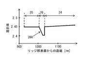
- It is a figure showing an example of refractive index distribution when a composition block is provided in a carrier block layer. It is a figure showing an example of the relationship between the thickness of the graded layer of FIG.
- FIG. 7 is a view showing a modified example of the cross-sectional configuration of the semiconductor laser of FIG. 1;
- FIG. 7 is a view showing a modified example of the cross-sectional configuration of the semiconductor laser of FIG. 1;
- FIG. 7 is a view showing a modified example of the cross-sectional configuration of the semiconductor laser of FIG. 1;
- It is a figure showing an example of outline composition of a projector by which the above-mentioned semiconductor laser is applied.
- It is a figure showing an example of a schematic structure of a display with which the above-mentioned semiconductor laser is applied.
- It is a figure showing an example of the perspective view composition of the electronic equipment to which the above-mentioned semiconductor laser is applied.
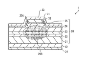
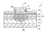
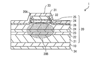
- FIG. 1 shows an example of the cross-sectional configuration of the semiconductor laser 1 according to the present embodiment.
- the semiconductor laser 1 has a structure in which a semiconductor laminated portion 20 described later is sandwiched between a pair of resonator end faces from the resonator direction (the extending direction of the ridge portion 20A). Accordingly, the semiconductor laser 1 is a kind of so-called edge-emitting semiconductor laser.
- the semiconductor laser 1 is provided with a semiconductor lamination portion 20 on a substrate 10.
- the semiconductor stacked unit 20 includes, for example, the lower cladding layer 21, the lower guide layer 22, the active layer 23, the low concentration impurity layer 24, and the contact layer 25 in this order from the substrate 10 side.
- the lower cladding layer 21 corresponds to one specific example of the “first cladding layer” of the present disclosure.
- the semiconductor stacked unit 20 may further be provided with a layer (for example, a buffer layer) other than the above-described layers. Further, in the semiconductor lamination portion 20, the lower guide layer 22 may be omitted.
- III-V nitride semiconductor refers to at least one of the 3B group elements in the short period periodic table (at least one element of Ga, Al, In, and B) It refers to one containing at least an N element of the 5B group elements in the periodic periodic table.
- III-V nitride semiconductors include gallium nitride-based compounds containing Ga and N.
- the gallium nitride-based compound includes, for example, GaN, AlGaN, AlGaInN and the like.
- p-type impurities are doped.
- the substrate 10 may be, for example, AlN, Al 2 O 3 (sapphire), SiC, Si, or Zr0.
- the substrate 10 may be a III-V nitride semiconductor substrate such as a GaN substrate.
- the crystal plane of the main surface of the GaN substrate may be any of a polar plane, a semipolar plane, and a nonpolar plane.
- Polar planes are represented, for example, as ⁇ 0, 0, 0, 1 ⁇ or ⁇ 0, 0, 0 -1 ⁇ using plane indices.
- the semipolar plane is, for example, ⁇ 2, 0, -2, 1 ⁇ , ⁇ 1, 0, -1, 1 ⁇ , ⁇ 2, 0, -2, -1 ⁇ , or ⁇ 1 using an area index.
- 0, -1, -1 ⁇ is represented, for example, as ⁇ 1, 1, ⁇ 2, 0 ⁇ or ⁇ 1, ⁇ 1, 0, 0 ⁇ using an area index.
- the lower cladding layer 21 is formed, for example, on the main surface of the substrate 10, and is formed of, for example, a semiconductor layer (n-type semiconductor layer) having n-type conductivity.
- the lower cladding layer 21 is formed of, for example, one of a GaN layer, an AlGaN layer, and an AlGaInN layer, or at least two of these layers.
- Si is used as a dopant for obtaining n-type conductivity.
- the film thickness of the lower cladding layer 21 is, for example, 500 nm to 3000 nm.
- the lower guide layer 22 is formed, for example, on the lower cladding layer 21 and is formed of, for example, an n-type semiconductor layer.
- the lower guide layer 22 is formed of, for example, one of a GaN layer, an AlGaN layer, an InGaN layer, and an AlGaInN layer, or at least two of these layers.
- Si is used as a dopant for obtaining n-type conductivity.
- the film thickness of the lower guide layer 22 is, for example, 10 nm to 500 nm.
- the lower guide layer 22 may be composed of a non-doped semiconductor layer.
- the active layer 23 is formed, for example, on the lower guide layer 22.
- the active layer 23 is provided between the lower guide layer 22 and the low concentration impurity layer 24.
- the active layer 23 is formed, for example, by alternately stacking barrier layers and well layers, and has a multi-well structure.
- the active layer 23 may have a multiple quantum well structure.
- Each well layer is composed of a Ga, III-V nitride semiconductor.
- Each well layer is formed of, for example, an n-type semiconductor layer.
- Si is used as a dopant for obtaining n-type conductivity.
- the film thickness of each well layer is, for example, 1 nm to 100 nm.
- Each well layer may be constituted by a non-doped semiconductor layer.
- the photon wavelength generated from each well layer is, for example, 430 nm to 550 nm.
- Each barrier layer is made of a group III-V nitride semiconductor.
- Each barrier layer is formed of, for example, an n-type semiconductor layer.
- In each barrier layer for example, Si is used as a dopant for obtaining n-type conductivity.
- the film thickness of each barrier layer is, for example, 1 nm to 100 nm.
- Each barrier layer may be constituted by a non-doped semiconductor layer.
- the band gap of the barrier layer is, for example, equal to or larger than the band gap which is the maximum in each well layer.
- the low concentration impurity layer 24 is formed, for example, on the active layer 23, and is formed of, for example, an n-type semiconductor layer.
- the low concentration impurity layer 24 is formed of, for example, one of a GaN layer, an AlGaN layer, an InGaN layer, and an AlGaInN layer, or at least two of these layers.
- the low concentration impurity layer 24 contains an impurity.
- the impurities refer to elements other than the elements constituting the III-V nitride semiconductor (specifically, at least one element of Ga, Al, In, and B and the N element).
- the impurities are composed of, for example, at least one or more elements of Mg, C, Si, and O.
- the concentration of the impurities contained in the low concentration impurity layer 24 is 5.0 ⁇ 10 17 cm ⁇ 3 or less, for example, 5.0 ⁇ 10 16 cm ⁇ 3 .
- the film thickness of the low concentration impurity layer 24 is 250 nm or more and 1000 nm or less, preferably 500 nm or more and 1000 nm or less in a portion facing the ridge portion 20A.
- the low concentration impurity layer 24 is provided not only at the bottom of the ridge portion 20A, but also at the side portion of the ridge portion 20A. Therefore, the film thickness of the portion immediately below the ridge portion 20A described later is larger than the film thickness of the portion beside the ridge portion 20A.
- the concentration of the impurities contained in the low concentration impurity layer 24 By setting the concentration of the impurities contained in the low concentration impurity layer 24 to 5.0 ⁇ 10 17 cm -3 or less, it is possible to reduce or avoid the deterioration of the light output characteristics due to the light absorption caused by the impurities. . Further, by setting the film thickness of the low concentration impurity layer 24 to 250 nm or more in the portion facing the ridge portion 20A, deterioration of the light output characteristics due to light absorption of the contact layer 25 and the upper cladding layer 31 is reduced or avoided. can do. Further, by setting the film thickness of the low concentration impurity layer 24 to 1000 nm or less at the portion facing the ridge portion 20A, it is possible to reduce or avoid the deterioration of the electrical characteristics due to the increase of the resistance component of the semiconductor layer.
- the impurity concentration and the composition ratio of constituent materials do not need to be uniform in the layer, and the low concentration impurity layer 24 may be a plurality of layers having different impurity concentrations and composition ratios of constituent materials. It may be configured. At that time, the total film thickness (total film thickness) is 250 nm or more and 1000 nm or less, preferably 500 nm or more and 1000 nm or less.
- a layer (for example, a carrier block layer or a cladding layer) different from the low concentration impurity layer 24 and thinner than the low concentration impurity layer 24 may be inserted into the low concentration impurity layer 24.
- the contact layer 25 is formed, for example, on the low concentration impurity layer 24, and is formed of, for example, a semiconductor layer (p-type semiconductor layer) having p-type conductivity.
- the contact layer 25 is formed of, for example, one of a GaN layer, an AlGaN layer, and an AlGaInN layer, or at least two of these layers.
- Mg is used as a dopant for obtaining p-type conductivity.
- the film thickness of the contact layer 25 is, for example, 1 nm or more and 150 nm or less. At this time, the distance between the low concentration impurity layer 24 and the upper cladding layer 31 is equal to the film thickness of the contact layer 25 and is, for example, 1 nm or more and 150 nm or less.
- a convex ridge portion 20A is formed in the upper portion of the semiconductor stacked portion 20, specifically, in a part of the low concentration impurity layer 24 and the contact layer 25.
- the contact layer 25 is formed on the top surface of the ridge portion 20A.
- the ridge portion 20A has a ridge shape extending in one direction (resonator direction) in the lamination plane of the semiconductor lamination portion 20 in a portion including the contact layer 25.
- the ridge portion 20A is sandwiched by a pair of resonator end faces in the semiconductor lamination portion 20.
- the length of the ridge portion 20A is, for example, 50 ⁇ m to 3000 ⁇ m.
- the width (length in the direction orthogonal to the resonator direction) of the ridge portion 20A is, for example, 0.5 ⁇ m to 100 ⁇ m.
- the ridge portion 20A is formed, for example, by etching away from the surface of the contact layer 25 to the middle of the low concentration impurity layer 24.
- the side surface and the bottom portion of the ridge portion 20 ⁇ / b> A in the upper surface of the semiconductor lamination portion 20 are covered with the insulating layer 32.
- the insulating layer 32 is made of, for example, SiO 2 .
- the film thickness of the insulating layer 32 is, for example, 10 nm to 500 nm.
- the semiconductor laser 1 further includes an upper cladding layer 31, an insulating layer 32, and an upper electrode layer 33 on the semiconductor multilayer portion 20, and a lower electrode layer 34 on the back surface side of the semiconductor multilayer portion 20.
- the upper cladding layer 31 corresponds to one specific example of the “second cladding layer” of the present disclosure.
- the upper cladding layer 31 is formed on the semiconductor lamination portion 20 and in contact with the upper surface of the ridge portion 20A.
- the upper cladding layer 31 is formed on the contact layer 25.
- the upper cladding layer 31 is formed of a transparent conductive material.
- a transparent conductive material which comprises the upper clad layer 31 ITO (Indium Tin Oxide), ITiO (Indium Titanium Oxide), etc. are mentioned.
- the film thickness of the upper cladding layer 31 is 10 nm or more and 500 nm or less.
- the upper cladding layer 31 may be electrically connected to the contact layer 25, and the layer configuration is not limited to the above configuration.
- the upper cladding layer 31 may be in contact with the entire top surface of the contact layer 25 or may be in contact with only a part of the top surface of the contact layer 25.
- the upper electrode layer 33 is formed on the upper cladding layer 31.
- the upper electrode layer 33 has, for example, a structure in which a Ti layer, a Pt layer, and an Au layer are stacked in this order from the side closer to the upper cladding layer 31.
- the film thickness of the Ti layer is, for example, 2 nm to 100 nm.
- the film thickness of the Pt layer is, for example, 10 nm to 300 nm.
- the thickness of the Au layer is, for example, 10 nm to 300 nm.
- the upper electrode layer 33 may be electrically connected to the upper cladding layer 31, and the layer configuration is not limited to the above-described configuration.
- the upper electrode layer 33 may be in contact with the entire upper surface of the upper cladding layer 31 or may be in contact with only a part of the upper surface of the upper cladding layer 31.
- the lower electrode layer 34 is formed, for example, in contact with the back surface of the substrate 10.
- the lower electrode layer 34 has, for example, a structure in which a Ti layer and an Al layer are stacked in this order from the side close to the substrate 10.
- the film thickness of the Ti layer is, for example, 5 nm to 50 nm.
- the film thickness of the Al layer is, for example, 10 nm to 300 nm.
- the lower electrode layer 34 may be electrically connected to the substrate 10, and the layer configuration thereof is not limited to the above configuration.
- the lower electrode layer 34 may be in contact with the entire back surface of the substrate 10 or may be in contact with only a part of the back surface of the substrate 10.
- a substrate 10 made of, for example, GaN is prepared.
- the lower cladding layer 21 and the lower guide layer 22 are epitaxially grown, for example, at a growth temperature of 1050 ° C. on the surface of the substrate 10 by, for example, MOCVD (Metal Organic Chemical Vapor Deposition; metal organic chemical vapor deposition) method.
- MOCVD Metal Organic Chemical Vapor Deposition; metal organic chemical vapor deposition
- the active layer 23 is epitaxially grown, for example, at a growth temperature of 700 ° C. by, eg, MOCVD.
- the low concentration impurity layer 24 and the contact layer 25 are epitaxially grown, for example, at a growth temperature of 1050 ° C. by the MOCVD method.
- trimethylgallium ((CH 3 ) 3 Ga) is used as a gallium source gas, and trimethyl aluminum ((CH 3 ) 3 Al) and indium are a source gas for aluminum.
- trimethyl indium ((CH 3 ) 3 In).
- ammonia (NH 3 ) is used as a nitrogen source gas.
- monosilane SiH 4
- a resist coating film is formed on the semiconductor lamination portion 20 with the region where the upper cladding layer 31 is to be formed as an opening, and the upper cladding layer 31 is formed by, for example, vacuum evaporation or sputtering. Subsequently, at least a part of the upper cladding layer 31, the contact layer 25, and the low concentration impurity layer 24 is removed by etching, for example, by the RIE method. Thus, the ridge portion 20A is formed, and the upper cladding layer 31 is formed on the ridge portion 20A.
- the insulating layer 32 is formed on the surface of the semiconductor multilayer portion 20 exposed by the above-described etching using, for example, a vacuum evaporation method or sputtering method, and the lift-off method is formed on the surfaces of the upper cladding layer 31 and the insulating layer 32.
- the upper electrode layer 33 is formed.
- the lower electrode layer 34 is formed on the back surface of the substrate 10 by, for example, a lift-off method.
- the substrate 10 is cut into a bar shape, and a coating film for controlling the reflectance is formed on the exposed end face portion.
- the semiconductor laser 1 is manufactured by cutting out the elements from the substrate 10 cut into the bar shape and forming the elements into chips.
- the optical waveguide region 20B is generated in a region directly below the ridge portion 20A with the active layer 23 at the center.
- the boundary of the light guiding region 20B (the portion indicated by the broken line in FIG. 1) is a region where the light intensity ratio is 0.007 with respect to the maximum value of the light intensity in the light guiding region 20B.
- the boundary of the light guiding region 20B is defined by the above definition because the light intensity ratio at the interface of the upper cladding layer 31 and the light absorption loss are in the relationship as shown in FIG. Do.
- FIG. 2 shows that when the light intensity ratio at the interface of the upper cladding layer 31 becomes larger than 0.007, the light absorption loss rapidly increases and the laser characteristics deteriorate. That is, when the upper cladding layer 31 is in contact with the light guiding region 20B, the light absorption loss is very large, and the laser characteristics are degraded. On the other hand, when the upper cladding layer 31 is at a distance from the light guiding region 20B, the light absorption loss is small, and the deterioration of the laser characteristics can be suppressed.
- FIG. 3 shows an example of the cross-sectional configuration of a general nitride-based semiconductor laser 100 (semiconductor laser 100 according to comparative example A).
- semiconductor laser 100 semiconductor laser 100 according to comparative example A.
- an AlGaN layer is generally used as a cladding layer in order to obtain a step of refractive index required to realize light confinement in the stacking direction.
- the semiconductor stacked portion 120 is provided on the substrate 10, and the upper guide layer 121 and the upper cladding layer 122 are provided instead of the low concentration impurity layer 24 according to the present embodiment. . Further, in the semiconductor laser 100, an upper electrode layer 131 made of ITO is provided on the ridge portion 120A instead of the upper cladding layer 31.
- the AlGaN cladding layer needs to carry out carrier transport while being required to have a low refractive index. Therefore, an AlGaN clad layer (lower clad layer 21) having n-type conductivity and an AlGaN clad layer (upper clad layer 122) having p-type conductivity on the other side are formed on both sides of the active layer 23.
- Mg is often doped into the upper cladding layer 122 as an acceptor in order to realize p-type conductivity.
- Mg in AlGaN has a large activation energy for ionization, and it is difficult to generate a high concentration of hole carriers. Therefore, the resistance of the upper cladding layer 122 becomes high, which causes the driving voltage of the semiconductor laser 100 to rise, and the power conversion efficiency of the semiconductor laser 100 is lowered.
- FIG. 4 schematically illustrates the cross-sectional configuration of the semiconductor laser 200 according to the comparative example B.
- the upper cladding layer 122 and the ridge portion 120A are not provided, the contact layer 123 contacts the upper guide layer 121, and the upper cladding layer 132 made of ITO instead of the upper electrode layer 131 is It is provided.
- an insulating layer 124 is provided around the upper cladding layer 132.
- the refractive index of ITO is, for example, about 2.0 for a wavelength of 450 nm, and has a value sufficiently smaller than the refractive index 2.5 of the upper guide layer 121. Therefore, the upper cladding layer 132 functions as a cladding layer that realizes a step of refractive index to realize light confinement in the stacking direction. In the semiconductor laser 200, since it is not necessary to use the p-type conductive AlGaN cladding layer having high resistance, the effect of reducing the driving voltage can be obtained.
- the ridge portion 120A is formed, and the insulating layer 32 is formed around the ridge portion 120A.
- the insulating layer 32 is formed of, for example, SiO 2 , and its refractive index is sufficiently smaller than that of the nitride semiconductor, for example, 1.46 for a wavelength of 450 nm. Therefore, it is possible to obtain the step of the refractive index necessary to realize the light confinement in the width direction of the ridge portion 120A, and it is possible to realize the stable laser operation.
- the upper cladding layer 132 is formed on the contact layer 123, and the insulating layer 124 is formed in the region where the upper cladding layer 132 is not formed.
- the refractive index of the insulating layer 124 is sufficiently larger than, for example, the refractive index 2.0 for the wavelength of 1.46 and the upper cladding layer 132 for the wavelength 450 nm. Therefore, even if the ridge portion is not formed, light confinement in the in-plane direction can be realized, stable laser operation can be obtained, and cost reduction and a good yield can be obtained.
- the upper cladding layer 132 has finite light absorption for light with a wavelength of, for example, 430 nm to 550 nm. Therefore, in the semiconductor laser 200, in the optical transverse mode formed in the resonator, the light intensity permeating into the upper cladding layer 132 is large (see the optical waveguide region 220B in FIG. 4). As a result, since the loss due to the light absorption of the upper cladding layer 132 is received, the characteristic improvement as the semiconductor laser 200 can not be sufficiently obtained. In addition, in the structure of the semiconductor lamination portion 220, light confinement in the in-plane direction of the lamination becomes insufficient, and the operation of the semiconductor laser 200 may become unstable.
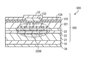
- FIG. 5 schematically shows a cross-sectional configuration of a semiconductor laser 300 according to Comparative Example C.
- a thick upper guide layer 321 is provided instead of the thin upper guide layer 121.
- the light intensity that leaks into the upper cladding layer 132 can be reduced (see the optical waveguide region 320B in FIG. 5).
- the upper cladding layer 132 is far away from the active layer 23, the light confinement in the in-plane direction of the laminated layer becomes insufficient, and there is a possibility that a stable laser operation can not be obtained.
- the upper cladding layer 31 is formed of a transparent conductive material. Furthermore, in the low concentration impurity layer 24 provided between the active layer 23 and the contact layer 25, the impurity concentration is 5.0 ⁇ 10 17 cm ⁇ 3 or less, and the total thickness of the low concentration impurity layer 24 is Is 250 nm or more and 1000 nm or less. Furthermore, the distance between the low concentration impurity layer 24 and the upper cladding layer 31 is 150 nm or less. Thereby, the light absorption by the transparent conductive material is suppressed, and further, even in the case where the thick clad layer made of Mg-doped AlGaN is not provided, the upper clad layer 31 formed of the transparent conductive material Be trapped. In the present embodiment, a band-like ridge portion 20A is further formed. Thereby, light is confined also in the lateral direction. As a result, the drive voltage can be suppressed.
- the upper cladding layer 31 is formed of a transparent conductive material. Furthermore, in the low concentration impurity layer 24 provided between the active layer 23 and the contact layer 25, the impurity concentration is 5.0 ⁇ 10 17 cm ⁇ 3 or less. Furthermore, the upper cladding layer 31 is provided at a distance from the optical waveguide region 20B generated in the semiconductor multilayer portion 20 when the semiconductor laser 1 is driven. That is, the light intensity ratio to the maximum value of the light intensity at the boundary position on the side closer to the active layer 23 of the upper cladding layer 31 is smaller than 0.007.
- the light absorption by the transparent conductive material is suppressed, and further, even in the case where the thick clad layer made of Mg-doped AlGaN is not provided, the upper clad layer 31 formed of the transparent conductive material Be trapped.
- a band-like ridge portion 20A is further formed. Thereby, light is confined also in the lateral direction. As a result, the drive voltage can be suppressed.
- FIG. 6 shows an example of the IV characteristics of the semiconductor laser 100 according to Comparative Example A, the semiconductor laser 200 according to Comparative Example B, and the semiconductor laser 1 according to the example.
- the results of FIG. 6 are derived by a semiconductor simulator.
- the impurity concentration of the low concentration impurity layer 24 is set to 2.0 ⁇ 10 16 cm ⁇ 3 and the film thickness of the low concentration impurity layer 24 is set to 500 nm.
- the impurity concentration of the upper guide layer 121 is 2.0 ⁇ 10 16 cm ⁇ 3 and the film thickness of the upper guide layer 121 is 200 nm. It can be seen from FIG. 6 that in the example, the drive voltage is lower than in Comparative Examples A and B.
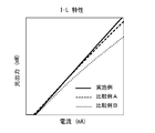
- FIG. 7 shows an example of the IL characteristics of the semiconductor laser 100 according to Comparative Example A, the semiconductor laser 200 according to Comparative Example B, and the semiconductor laser 1 according to the example. It can be seen from FIG. 7 that in the example, higher light output is obtained as compared with Comparative Examples A and B.
- FIG. 8 shows an example of the L-WPE (power conversion efficiency) characteristics of the semiconductor laser 100 according to the comparative example A, the semiconductor laser 200 according to the comparative example B, and the semiconductor laser 1 according to the example. It can be seen from FIG. 8 that in the example, higher power conversion efficiency is obtained as compared with Comparative Examples A and B.
- the semiconductor stacked portion 20 (the lower cladding layer 21, the active layer 23, the low concentration impurity layer 24 and the contact layer 25) is formed of a nitride semiconductor.
- the upper cladding layer 31 is formed of ITO or ITiO.
- the driving voltage can be suppressed as compared with the case where a thick film cladding layer made of Mg-doped AlGaN is provided.
- FIGS. 9 to 14 show a modification of the cross-sectional configuration of the semiconductor laser 1.
- the contact layer 25 may be formed of a thick film, for example, as shown in FIG.
- the ridge portion 20A may be formed, for example, by etching a part of the contact layer 25.
- the film thickness of the portion immediately below the ridge portion 20A may be larger than the film thickness of the portion beside the ridge portion 20A.
- the light absorption by the transparent conductive material is suppressed, and, for example, the upper clad layer formed of the transparent conductive material without providing a thick clad layer made of Mg-doped AlGaN.
- Light 31 is confined in the stacking direction by 31. Furthermore, the light is confined also in the lateral direction by the ridge portion 20A. As a result, the drive voltage can be suppressed.
- the semiconductor laser 1 has, for example, the carrier block layer 26 which is a layer different from the low concentration impurity layer 24 with respect to the low concentration impurity layer 24 as shown in FIG. It may be inserted. At this time, the carrier block layer 26 is inserted between the active layer 23 and the contact layer 25. At this time, in the low concentration impurity layer 24, the film thickness of the portion immediately below the ridge portion 20A is thicker than the film thickness of the portion beside the ridge portion 20A. The carrier block layer 26 prevents carriers injected from the substrate 10 side from penetrating the active layer 23 into the ridge portion 20A. By providing the carrier block layer 26, the utilization efficiency of carriers can be improved, and the power conversion efficiency of the semiconductor laser 1 can be improved.
- the carrier block layer 26 is configured of, for example, a p-type semiconductor layer.
- the carrier block layer 26 is formed of, for example, one of a GaN layer, an AlGaN layer, an InGaN layer, and an AlGaInN layer, or at least two of these layers.
- Mg is used as a dopant for obtaining p-type conductivity.
- the film thickness of the carrier block layer 26 is, for example, 3 nm to 50 nm.
- a carrier block layer 26 which is a layer different from the low concentration impurity layer 24 is inserted into the low concentration impurity layer 24.
- the light absorption by the transparent conductive material is suppressed, and, for example, the upper clad layer formed of the transparent conductive material without providing a thick clad layer made of Mg-doped AlGaN.
- Light 31 is confined in the stacking direction by 31. Furthermore, the light is confined also in the lateral direction by the ridge portion 20A. As a result, the drive voltage can be suppressed.
- the ridge portion 20A may be formed by etching a part of the contact layer 25, the carrier block layer 26, and the low concentration impurity layer 24. .
- the film thickness of the portion immediately below the ridge portion 20A is thicker than the film thickness of the portion beside the ridge portion 20A. There is. With such a configuration, the light confinement in the lateral direction by the ridge portion 20A is further strengthened, and good light output characteristics can be obtained.
- the transparent conductive material is suppressed, and furthermore, light is confined in the stacking direction by the upper cladding layer 31 formed of the transparent conductive material, even without providing a thick cladding layer made of Mg-doped AlGaN, for example. .
- the drive voltage can be suppressed.
- the composition of the carrier block layer 25 may be inclined so that the band gap energy of the carrier block layer 26 decreases toward the contact layer 25 side.
- the carrier block layer 26 is formed of the graded layer 26A in which the composition of the carrier block layer 25 is inclined so that the band gap energy decreases toward the contact layer 25 side.
- the composition gradient (graded layer 26A) of the carrier block layer 26 suppresses electron overflow. it can.
- the concentration of holes collected at the interface between the carrier block layer 26 and the contact layer 25 can also be reduced by the composition gradient of the carrier block layer 25 (graded layer 26A).
- graded layer 26A the composition gradient of the carrier block layer 25
- the graded layer 26A is made thicker, the amount of decrease in the hole concentration at the interface between the carrier block layer 26 and the contact layer 25 increases.
- the ridge portion 20A is formed by etching the carrier block layer 26.
- holes accumulated at the interface between the carrier block layer 26 and the contact layer 25 disappear due to non-radiative recombination that occurs on the surface of the etched ridge portion 20A.
- Holes accumulated at the interface between the carrier block layer 26 and the contact layer 25 can easily move in the ridge portion 20A as a two-dimensional electron gas. Therefore, as the concentration of holes collected at the interface between the carrier block layer 26 and the contact layer 25 increases, the number of holes eliminated in the non-emission recombination process increases, and the light emission efficiency decreases.
- the composition of the carrier block layer 26 is inclined so that the band gap energy of the carrier block layer 26 decreases toward the contact layer 25.
- the concentration of holes collected at the interface decreases.
- the carrier block layer 26 may be inserted between the active layer 23 and the low concentration impurity layer 24. Even in this case, the light absorption by the transparent conductive material is suppressed, and, for example, the upper clad layer formed of the transparent conductive material without providing a thick clad layer made of Mg-doped AlGaN.
- Light 31 is confined in the stacking direction by 31. Furthermore, the light is confined also in the lateral direction by the ridge portion 20A. As a result, the drive voltage can be suppressed.
- the carrier block layer 26 may be inserted between the low concentration impurity layer 24 and the contact layer 25.
- the contact layer 25 may be a thick film, and a part of the contact layer 25 may be etched to form the ridge portion 20A, and the carrier block layer 26 may be formed in contact with the contact layer 25. .
- the light absorption by the transparent conductive material is suppressed, and, for example, the upper clad layer formed of the transparent conductive material without providing a thick clad layer made of Mg-doped AlGaN.
- Light 31 is confined in the stacking direction by 31. Furthermore, the light is confined also in the lateral direction by the ridge portion 20A. As a result, the drive voltage can be suppressed.
- the semiconductor laser 1 may have the upper cladding layer 27 between the contact layer 25 and the low concentration impurity layer 24 as shown in FIG. 16, for example.
- the upper cladding layer 27 is, for example, a Mg-doped AlGaN layer, and has a thickness smaller than that of the low concentration impurity layer 24 in a portion facing the ridge portion 20A.
- the total film thickness of the contact layer 25 and the upper cladding layer 31 is, for example, 150 nm or less.
- the light absorption by the transparent conductive material is suppressed, and, for example, the upper clad layer formed of the transparent conductive material without providing a thick clad layer made of Mg-doped AlGaN.
- Light 31 is confined in the stacking direction by 31. Furthermore, the light is confined also in the lateral direction by the ridge portion 20A. As a result, the drive voltage can be suppressed.
- the semiconductor stacked unit 20 is made of a III-V group semiconductor including any one of As, B, Sb, and P, or at least two of them. It may be Even in this case, the light is confined in the stacking direction by the upper cladding layer 31, and the light is confined in the lateral direction by the ridge portion 20A. As a result, the drive voltage can be suppressed.
- a metal layer or a resin layer may be provided instead of the insulating layer 32.
- the insulating layer 32 is omitted, and further, the portion around the ridge portion 20A and the bottom portion of the semiconductor laminated portion 20 (that is, the portion in contact with the insulating layer 32). ) May be exposed to the atmosphere. Even in this case, the light is confined in the stacking direction by the upper cladding layer 31, and the light is confined in the lateral direction by the ridge portion 20A. As a result, the drive voltage can be suppressed.
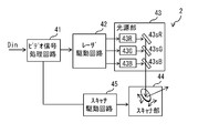
- FIG. 17 illustrates an example of a schematic configuration of the projector 2.
- the projector 2 is an apparatus for projecting an image based on an image signal Din input from the outside on a screen or the like.
- the projector 2 includes a video signal processing circuit 41, a laser drive circuit 42, a light source unit 43, a scanner unit 44 and a scanner drive circuit 45.
- the video signal processing circuit 41 generates a projection video signal for each color based on the video signal Din.
- the laser drive circuit 42 controls the peak value of the current pulse applied to the light sources 43R, 43G, 43B described later based on the projection video signal for each color.
- the light source unit 43 has a plurality of light sources, for example, three light sources 43R, 43G, and 43B.
- the three light sources 43R, 43G, and 43B are used, for example, as laser light sources that emit laser light of red (R), green (G), and blue (B) wavelengths.
- At least one of the light sources 43B and 43G includes the semiconductor laser 1 according to the above-described embodiment and the modification thereof.
- the laser beams emitted from the three light sources 43R, 43G, and 43B for example, are collimated into substantially parallel beams by a collimator lens, and then bundled into one laser beam by beam splitters 43sR, 43sG, and 43sB.
- the beam splitter 43sR reflects, for example, red light.
- the beam splitter 43sG reflects, for example, green light and transmits red light.
- the beam splitter 43sB reflects, for example, blue light and transmits red light and green light.
- the scanner unit 44 is configured using, for example, one two-axis scanner.
- the incident laser light is modulated to the irradiation angle in the horizontal and vertical directions by the two-axis scanner and then projected onto the screen.
- the scanner unit 44 may be configured to scan horizontally and vertically using two single-axis scanners.
- the scanner unit 44 has a sensor for detecting an irradiation angle such as a two-axis scanner, and the sensor outputs angle signals of horizontal and vertical respectively. These angle signals are input to the scanner drive circuit 45.
- the scanner drive circuit 45 drives the scanner unit 44 to a desired irradiation angle based on, for example, the horizontal angle signal and the vertical angle signal input from the scanner unit 44.
- the semiconductor laser 1 according to the above-described embodiment and its modification is used. Thereby, high emission intensity can be obtained with low power consumption.
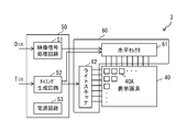
- FIG. 18 illustrates a schematic configuration example of the display device 3.
- the display device 3 includes, for example, a pixel array unit 40, a controller 50, and a driver 60.
- the pixel array unit 40 includes a plurality of display pixels 40A arranged in a matrix.
- the controller 50 and the driver 60 drive each display pixel 40A based on the video signal Din and the synchronization signal Tin input from the outside.
- the pixel array unit 40 displays an image based on the externally input video signal Din and the synchronization signal Tin by active matrix driving of each display pixel 40A by the controller 50 and the driver 60.
- the pixel array unit 40 includes a plurality of scanning lines extending in the row direction, a plurality of signal lines extending in the column direction, and a plurality of scanning lines and signal lines crossing each other. And the display pixel 40A.
- the scanning line is used to select each display pixel 40A, and supplies a selection pulse for selecting each display pixel 40A for each predetermined unit (for example, pixel row) to each display pixel 40A.
- the signal line is used to supply a signal voltage corresponding to the video signal Din to each display pixel 40A, and supplies a data pulse including the signal voltage to each display pixel 40A.
- Each display pixel 40A has a plurality of sub-pixels each including a semiconductor laser.
- at least one of the semiconductor lasers emitting blue light and green light among the plurality of sub-pixels is the semiconductor laser 1 according to the above-described embodiment and its modification.
- the driver 60 includes, for example, a horizontal selector 61 and a light scanner 62.
- the horizontal selector 61 applies an analog signal voltage input from the video signal processing circuit 51 to each signal line, for example, in response to (in synchronization with) an input of a control signal from the controller 50.
- the light scanner 62 scans the plurality of display pixels 40A in predetermined units. Specifically, the write scanner 62 sequentially outputs selection pulses to each scanning line in one frame period.
- the write scanner 62 executes the writing of the signal voltages in a desired order by, for example, selecting (in synchronization with) a plurality of scanning lines in a predetermined sequence in response to (in synchronization with) input of a control signal from the controller 50.
- the controller 50 includes, for example, a video signal processing circuit 51, a timing generation circuit 52, and a power supply circuit 53.
- the video signal processing circuit 51 performs predetermined correction on the digital video signal Din input from the outside, and generates a signal voltage based on the video signal obtained thereby.
- the video signal processing circuit 51 outputs, for example, the generated signal voltage to the horizontal selector 61.
- the timing generation circuit 52 controls each circuit in the driver 60 to operate in conjunction.
- the timing generation circuit 52 outputs a control signal to each circuit in the driver 60, for example, according to (in synchronization with) the synchronization signal Tin input from the outside.
- the power supply circuit 53 generates and supplies various fixed voltages required for various circuits such as the horizontal selector 61, the write scanner 62, the video signal processing circuit 51, the timing generation circuit 52, and the power supply circuit 53.
- the semiconductor laser 1 according to the above-described embodiment or the variation thereof is used in each display pixel 40A. Thereby, high emission intensity can be obtained with low power consumption.
- FIG. 19 illustrates an example of a perspective view of the electronic device 4.
- the electronic device 4 is, for example, a portable terminal provided with a display surface on the main surface of a plate-like casing.
- the electronic device 4 includes, for example, the display device 3 according to the third embodiment at the position of the display surface.
- the pixel array unit 40 of the display device 3 is disposed on the display surface of the electronic device 4.
- the semiconductor laser 1 according to the above-described embodiment or the variation thereof is used in each display pixel 40A. Thereby, high emission intensity can be obtained with low power consumption.
- the display device 3 is a video signal input from the outside, such as a television device, a digital camera, a notebook personal computer, a portable terminal device such as a mobile phone or a video camera, or
- the generated video signal can be applied to a display device of an electronic device in any field that displays as an image or a video.
- the present disclosure can have the following configurations.
- the semiconductor laser according to (1) wherein the first cladding layer, the active layer, the low concentration impurity layer, and the contact layer are all formed of a nitride-based semiconductor material.
- the transparent conductive material is ITO or ITiO.
- a carrier block layer interposed between the active layer and the contact layer, In the low concentration impurity layer, the film thickness of the portion directly below the ridge shape is thicker than the film thickness of the side portion of the ridge shape according to any one of (1) to (4) Semiconductor laser.
- a semiconductor laser wherein a light intensity ratio to a maximum value of light intensity is smaller than 0.007 at a boundary position on the side closer to the active layer of the second cladding layer.
- the semiconductor laser has a semiconductor laser as a light source,
- the semiconductor laser is A first cladding layer, an active layer, one or more lightly doped impurity layers, a contact layer, and a second cladding layer formed of a transparent conductive material in this order, and in a portion including the contact layer
- An electronic device wherein a distance between the low concentration impurity layer closest to the second cladding layer and the second cladding layer is 150 nm or less.
- the semiconductor laser is A first cladding layer, an active layer, one or a plurality of low concentration impurity layers having an impurity concentration of 5.0 ⁇ 10 17 cm ⁇ 3 or less, a contact layer, and a second cladding layer formed of a transparent conductive material in this order
- a semiconductor laser including a semiconductor laminated portion having a ridge shape extending in one direction in the laminated plane in a portion including the contact layer,
- the second cladding layer is provided at a distance from an optical waveguide region generated in the semiconductor multilayer portion when the semiconductor laser is driven.
- the electronic device whose light intensity ratio with respect to the maximum value of the light intensity in the boundary position by the side near the said active layer of a said 2nd cladding layer is smaller than 0.007.
- the first semiconductor laser, the second semiconductor laser, the first electronic device, and the second electronic device According to the first semiconductor laser, the second semiconductor laser, the first electronic device, and the second electronic device according to an embodiment of the present disclosure, light absorption by the transparent conductive material is suppressed, and further, for example, Mg doped Even without providing a thick film cladding layer of AlGaN, light can be confined in the stacking direction by the second cladding layer formed of a transparent conductive material, and light can be confined also in the lateral direction by the strip ridge. Therefore, the drive voltage can be suppressed.
- the effects of the present disclosure are not necessarily limited to the effects described herein, but may be any of the effects described herein.
Landscapes
- Physics & Mathematics (AREA)
- Condensed Matter Physics & Semiconductors (AREA)
- General Physics & Mathematics (AREA)
- Electromagnetism (AREA)
- Optics & Photonics (AREA)
- Geometry (AREA)
- Semiconductor Lasers (AREA)
Abstract
本開示の一実施形態に係る半導体レーザは、半導体積層部を備えている。半導体積層部は、第1クラッド層、活性層、1または複数の低濃度不純物層、コンタクト層、および、透明導電材料で形成された第2クラッド層をこの順に含んでいる。半導体積層部は、さらに、コンタクト層を含む部分に積層面内の一の方向に延在するリッジ形状を有している。各低濃度不純物層において、不純物濃度が5.0×1017cm-3以下となっており、低濃度不純物層の総膜厚が250nm以上1000nm以下となっている。第2クラッド層に最も近い低濃度不純物層と第2クラッド層との距離が150nm以下となっている。
Description
本開示は、半導体レーザおよびそれを備えた電子機器に関する。
従来から、半導体レーザについての様々な技術が開示されている。
半導体レーザでは、輝度を高める観点から、高出力化が求められている。高出力化に伴い、発熱が問題となる。発熱量は電力変換効率により決まる。そのため、発熱量を抑えるためには、光出力特性だけでなく、駆動電圧の低減が重要となる。従って、駆動電圧を抑えることの可能な半導体レーザおよびそれを備えた電子機器を提供することが望ましい。
本開示の一実施形態に係る第1の半導体レーザは、半導体積層部を備えている。半導体積層部は、第1クラッド層、活性層、1または複数の低濃度不純物層、コンタクト層、および、透明導電材料で形成された第2クラッド層をこの順に含んでいる。半導体積層部は、さらに、コンタクト層を含む部分に積層面内の一の方向に延在するリッジ形状を有している。各低濃度不純物層において、不純物濃度が5.0×1017cm-3以下となっており、低濃度不純物層の総膜厚が250nm以上1000nm以下となっている。第2クラッド層に最も近い低濃度不純物層と第2クラッド層との距離が150nm以下となっている。
本開示の一実施形態に係る第2の半導体レーザは、半導体積層部を備えている。半導体積層部は、第1クラッド層、活性層、不純物濃度が5.0×1017cm-3以下の1または複数の低濃度不純物層、コンタクト層、および、透明導電材料で形成された第2クラッド層をこの順に含んでいる。半導体積層部は、さらに、コンタクト層を含む部分に積層面内の一の方向に延在するリッジ形状を有している。第2クラッド層は、当該半導体レーザが駆動されたときに半導体積層部内に生じる光導波領域から離れた位置に設けられている。
本開示の一実施形態に係る第1の電子機器は、上記の第1の半導体レーザを光源として備えている。
本開示の一実施形態に係る第2の電子機器は、上記の第2の半導体レーザを光源として備えている。
本開示の一実施形態に係る第1の半導体レーザおよび第1の電子機器では、第2クラッド層が透明導電材料で形成されている。さらに、活性層とコンタクト層との間に設けられた1または複数の低濃度不純物層において、不純物濃度が5.0×1017cm-3以下となっており、低濃度不純物層の総膜厚が250nm以上1000nm以下となっている。さらに、第2クラッド層に最も近い低濃度不純物層と第2クラッド層との距離が150nm以下となっている。これにより、透明導電材料による光吸収が抑えられ、さらに、例えばMgドープのAlGaNからなる厚膜のクラッド層を設けなくても、透明導電材料で形成された第2クラッド層によって光が積層方向において閉じ込められる。本開示の一実施形態に係る第1の半導体レーザおよび第1の電子機器では、さらに、帯状のリッジが形成されている。これにより、横方向においても光が閉じ込められる。
本開示の一実施形態に係る第2の半導体レーザおよび第2の電子機器では、第2クラッド層が透明導電材料で形成されている。さらに、活性層とコンタクト層との間に設けた1または複数の低濃度不純物層において、不純物濃度が5.0×1017cm-3以下となっている。さらに、第2クラッド層は、当該半導体レーザが駆動されたときに半導体積層部内に生じる光導波領域から離れた位置に設けられている。これにより、透明導電材料による光吸収が抑えられ、さらに、例えばMgドープのAlGaNからなる厚膜のクラッド層を設けなくても、透明導電材料で形成された第2クラッド層によって光が積層方向において閉じ込められる。本開示の一実施形態に係る第1の半導体レーザおよび第1の電子機器では、さらに、帯状のリッジが形成されている。これにより、横方向においても光が閉じ込められる。
以下、本開示を実施するための形態について、図面を参照して詳細に説明する。以下の説明は本開示の一具体例であって、本開示は以下の態様に限定されるものではない。また、本開示は、各図に示す各構成要素の配置や寸法、寸法比などについても、それらに限定されるものではない。なお、説明は、以下の順序で行う。
1.第1の実施の形態(半導体レーザ)
2.変形例(半導体レーザ)
3.第2の実施の形態(プロジェクタ)
4.第3の実施の形態(表示装置)
5.第4の実施の形態(電子機器)
1.第1の実施の形態(半導体レーザ)
2.変形例(半導体レーザ)
3.第2の実施の形態(プロジェクタ)
4.第3の実施の形態(表示装置)
5.第4の実施の形態(電子機器)
<1.第1の実施の形態>
[構成]
本開示の第1の実施の形態に係る半導体レーザ1について説明する。図1は、本実施の形態に係る半導体レーザ1の断面構成例を表したものである。半導体レーザ1は、後述の半導体積層部20を共振器方向(リッジ部20Aの延在方向)から一対の共振器端面によって挟み込んだ構造となっている。従って、半導体レーザ1は、いわゆる端面発光型の半導体レーザの一種である。
[構成]
本開示の第1の実施の形態に係る半導体レーザ1について説明する。図1は、本実施の形態に係る半導体レーザ1の断面構成例を表したものである。半導体レーザ1は、後述の半導体積層部20を共振器方向(リッジ部20Aの延在方向)から一対の共振器端面によって挟み込んだ構造となっている。従って、半導体レーザ1は、いわゆる端面発光型の半導体レーザの一種である。
半導体レーザ1は、基板10上に半導体積層部20を備えたものである。半導体積層部20は、例えば、下部クラッド層21、下部ガイド層22、活性層23、低濃度不純物層24およびコンタクト層25を基板10側からこの順に有している。下部クラッド層21が、本開示の「第1クラッド層」の一具体例に対応する。なお、半導体積層部20には、上記した層以外の層(例えばバッファ層など)がさらに設けられていてもよい。また、半導体積層部20において、下部ガイド層22が省略されていてもよい。
基板10および半導体積層部20は、例えば、GaNなどのIII-V族窒化物半導体で形成されている。ここで、「III-V族窒化物半導体」とは、短周期型周期率表における3B族元素群のうちの少なくとも1種(Ga,Al,InおよびBのうち少なくとも1つの元素)と、短周期型周期率表における5B族元素のうちの少なくともN元素とを含むものを指している。III-V族窒化物半導体としては、例えば、GaとNとを含んだ窒化ガリウム系化合物が挙げられる。窒化ガリウム系化合物には、例えば、GaN、AlGaN、AlGaInNなどが含まれる。III-V族窒化物半導体には、必要に応じてSi、Ge、O、SeなどのIV族またはVI族元素のn型不純物、または、Mg、Zn、CなどのII族またはIV族元素のp型不純物がドープされている。基板10は、例えば、AlN、Al2O3(サファイア)、SiC、Si、Zr0であってもよい。
基板10は、GaN基板などのIII-V族窒化物半導体基板であってもよい。この場合、GaN基板の主面の結晶面は、極性面、半極性面、非極性面のいずれでもよい。極性面は、例えば、面指数を用いて、{0,0,0,1}、または{0,0,0,-1}と表される。半極性面は、例えば、面指数を用いて、{2,0,-2,1}、{1,0,-1,1}、{2,0,-2,-1}、または{1,0,-1,-1}と表される。非極性面は、例えば、面指数を用いて、{1,1,-2,0}または{1,-1,0,0}と表される。
下部クラッド層21は、例えば、基板10の主面上に形成されており、例えば、n型導電性を有する半導体層(n型半導体層)によって構成されている。下部クラッド層21は、例えば、GaN層、AlGaN層およびAlGaInN層のうちのいずれか、またはこれらのうち少なくとも2つの層によって構成されている。下部クラッド層21において、n型導電性が得られるためのドーパントとして例えばSiが用いられている。下部クラッド層21の膜厚は、例えば、500nm~3000nmである。
下部ガイド層22は、例えば、下部クラッド層21上に形成されており、例えば、n型半導体層によって構成されている。下部ガイド層22は、例えば、GaN層、AlGaN層、InGaN層およびAlGaInN層のうちのいずれか、またはこれらのうち少なくとも2つの層によって構成されている。下部ガイド層22において、n型導電性が得られるためのドーパントとして例えばSiが用いられている。下部ガイド層22の膜厚は、例えば、10nm~500nmである。下部ガイド層22は、ノンドープの半導体層によって構成されていてもよい。
活性層23は、例えば、下部ガイド層22上に形成されている。活性層23は、下部ガイド層22と低濃度不純物層24との間に設けられている。活性層23は、例えば、障壁層および井戸層を交互に積層して構成されたものであり、多重井戸構造となっている。活性層23は、多重量子井戸構造となっていてもよい。
各井戸層は、Ga,III-V族窒化物半導体で構成されている。各井戸層は、例えば、n型半導体層によって構成されている。各井戸層において、n型導電性が得られるためのドーパントとして例えばSiが用いられている。各井戸層の膜厚は、例えば、1nm~100nmである。各井戸層は、ノンドープの半導体層によって構成されていてもよい。各井戸層から生成される光子波長は、例えば、430nm~550nmである。
各障壁層は、III-V族窒化物半導体で構成されている。各障壁層は、例えば、n型半導体層によって構成されている。各障壁層において、n型導電性が得られるためのドーパントとして例えばSiが用いられている。各障壁層の膜厚は、例えば、1nm~100nmである。各障壁層は、ノンドープの半導体層によって構成されていてもよい。障壁層のバンドギャップは、例えば、各井戸層において最大となるバンドギャップ以上の値となっている。
低濃度不純物層24は、例えば、活性層23上に形成されており、例えば、n型半導体層によって構成されている。低濃度不純物層24は、例えば、GaN層、AlGaN層、InGaN層およびAlGaInN層のうちのいずれか、またはこれらのうち少なくとも2つの層によって構成されている。低濃度不純物層24には、不純物が含まれている。ここで、不純物とは、III-V族窒化物半導体を構成する元素(具体的には、Ga,Al,InおよびBのうち少なくとも1つの元素と、N元素)以外の元素を指している。不純物は、例えば、Mg,C,Si,Oのうち少なくとも1つ以上の元素で構成されている。低濃度不純物層24に含まれる不純物の濃度は、5.0×1017cm-3以下となっており、例えば、5.0×1016cm-3となっている。低濃度不純物層24の膜厚は、リッジ部20Aと対向する部分において、250nm以上1000nm以下となっており、好ましくは500nm以上1000nm以下となっている。なお、本実施の形態では、低濃度不純物層24は、リッジ部20Aの底部に設けられているだけでなく、リッジ部20Aの脇の部分にも設けられている。そのため、後述のリッジ部20Aの直下の部分の膜厚が、リッジ部20Aの脇の部分の膜厚よりも厚くなっている。
低濃度不純物層24に含まれる不純物の濃度は、5.0×1017cm-3以下となっていることにより、不純物に起因する光吸収による光出力特性の劣化を低減、回避することができる。また、低濃度不純物層24の膜厚が、リッジ部20Aと対向する部分において、250nm以上となっていることにより、コンタクト層25や上部クラッド層31の光吸収による光出力特性劣化を低減、回避することができる。また、低濃度不純物層24の膜厚が、リッジ部20Aと対向する部分において、1000nm以下となっていることにより、半導体層の抵抗成分増大による電気特性の劣化を低減、回避することができる。
低濃度不純物層24において、不純物濃度や構成材料の組成比が層内で均一となっている必要はなく、低濃度不純物層24が、不純物濃度や構成材料の組成比が互いに異なる複数の層によって構成されていてもよい。その際、その合計の膜厚(総膜厚)が、250nm以上1000nm以下となっており、好ましくは500nm以上1000nm以下となっている。低濃度不純物層24に対して、低濃度不純物層24とは異なる、低濃度不純物層24の膜厚よりも薄い層(例えば、キャリアブロック層やクラッド層)が挿入されていてもよい。
コンタクト層25は、例えば、低濃度不純物層24上に形成されており、例えば、p型導電性を有する半導体層(p型半導体層)によって構成されている。コンタクト層25は、例えば、GaN層、AlGaN層およびAlGaInN層のうちのいずれか、またはこれらのうち少なくとも2つの層によって構成されている。コンタクト層25において、p型導電性が得られるためのドーパントとして例えばMgが用いられている。コンタクト層25の膜厚は、例えば、1nm以上150nm以下である。このとき、低濃度不純物層24と上部クラッド層31との距離は、コンタクト層25の膜厚と等しくなっており、例えば、1nm以上150nm以下となっている。
半導体積層部20の上部、具体的には、低濃度不純物層24の一部およびコンタクト層25において、凸状のリッジ部20Aが形成されている。コンタクト層25は、リッジ部20Aの上面に形成されている。リッジ部20Aは、コンタクト層25を含む部分に、半導体積層部20の積層面内の一の方向(共振器方向)に延在するリッジ形状を有している。リッジ部20Aは、半導体積層部20における一対の共振器端面によって挟み込まれている。リッジ部20Aの長さは、例えば、50μm~3000μmである。リッジ部20Aの幅(共振器方向と直交する方向の長さ)は、例えば、0.5μm~100μmである。リッジ部20Aは、例えば、コンタクト層25の表面から低濃度不純物層24の中途にかけてエッチング除去がなされることにより形成される。
半導体積層部20の上面のうちリッジ部20Aの側面および裾野部分は、絶縁層32によって覆われている。絶縁層32は、例えば、SiO2によって構成されている。絶縁層32の膜厚は、例えば、10nm~500nmである。
半導体レーザ1は、さらに、半導体積層部20上に、上部クラッド層31、絶縁層32および上部電極層33を備えており、半導体積層部20の裏面側に、下部電極層34を備えている。上部クラッド層31が、本開示の「第2クラッド層」の一具体例に対応する。
上部クラッド層31は、半導体積層部20上であって、かつ、リッジ部20Aの上面に接して形成されている。上部クラッド層31は、コンタクト層25上に形成されている。上部クラッド層31は、透明導電材料で形成されている。上部クラッド層31を構成する透明導電材料としては、ITO(Indium Tin Oxide)、または、ITiO(Indium Titanium Oxide)などが挙げられる。上部クラッド層31の膜厚は10nm以上500nm以下である。上部クラッド層31は、コンタクト層25と電気的に接続されていればよく、その層構成は上記の構成に限らない。また、上部クラッド層31は、コンタクト層25の上面全体と接触していてもよいし、コンタクト層25の上面の一部とだけ接していてもよい。
上部電極層33は、上部クラッド層31上に形成されている。上部電極層33は、例えば、Ti層、Pt層、Au層が上部クラッド層31に近い側からこの順に積層された構成となっている。Ti層の膜厚は、例えば、2nm~100nmである。Pt層の膜厚は、例えば、10nm~300nmである。Au層の膜厚は、例えば、10nm~300nmである。上部電極層33は、上部クラッド層31と電気的に接続されていればよく、その層構成は上記の構成に限らない。また、上部電極層33は、上部クラッド層31の上面全体と接触していてもよいし、上部クラッド層31の上面の一部とだけ接していてもよい。
下部電極層34は、例えば、基板10の裏面に接して形成されている。下部電極層34は、例えば、Ti層、Al層が基板10に近い側からこの順に積層された構成となっている。Ti層の膜厚は、例えば、5nm~50nmである。Al層の膜厚は、例えば、10nm~300nmである。下部電極層34は、基板10と電気的に接続されていればよく、その層構成は上記の構成に限らない。また、下部電極層34は、基板10の裏面全体と接触していてもよいし、基板10の裏面の一部とだけ接していてもよい。
[製造方法]
次に、半導体レーザ1の製造方法について説明する。
次に、半導体レーザ1の製造方法について説明する。
まず、例えばGaNよりなる基板10を用意する。次に、この基板10の表面に、例えば、MOCVD(Metal Organic Chemical Vapor Deposition ;有機金属化学気相成長)法により、下部クラッド層21および下部ガイド層22を、例えば成長温度1050℃にてエピタキシャル成長させる。次に、例えばMOCVD法により、活性層23を、例えば成長温度700℃にてエピタキシャル成長させる。次に、MOCVD法により、低濃度不純物層24およびコンタクト層25を、例えば成長温度1050℃にてエピタキシャル成長させる。
なお、MOCVDを行う際、ガリウムの原料ガスとしては、例えばトリメチルガリウム((CH3)3Ga)、アルミニウムの原料ガスとしては、例えばトリメチルアルミニウム((CH3)3Al)、インジウムの原料ガスとしては、例えばトリメチルインジウム((CH3)3In)をそれぞれ用いる。また、窒素の原料ガスとしては、アンモニア(NH3)を用いる。また、ケイ素の原料ガスとしては、例えばモノシラン(SiH4)を用い、マグネシウムの原料ガスとしては、例えばビス=シクロペンタジエニルマグネシウム((C5H5)2Mg)を用いる。
次に、半導体積層部20上に、上部クラッド層31を形成する領域を開口部としたレジストコート膜を形成し、上部クラッド層31を例えば、真空蒸着法やスパッタ法により形成する。続いて、例えばRIE法により、少なくとも上部クラッド層31、コンタクト層25および低濃度不純物層24の一部をエッチングにより除去する。これにより、リッジ部20Aを形成するとともに、リッジ部20A上に上部クラッド層31を形成する。
次に、上記エッチングにより露出した半導体積層部20の表面上に、例えば真空蒸着法やスパッタ法を用い、絶縁層32を形成し、上部クラッド層31および絶縁層32の表面上に、例えばリフトオフ法により、上部電極層33を形成する。次に、基板10の裏面上に、例えばリフトオフ法により、下部電極層34を形成する。次に、基板10をバー状に切出し、露出した端面部に反射率を制御するためのコーティング膜を形成する。さらに、バー状に切断された基板10から素子を切出し、チップ化することで、半導体レーザ1が作製される。
[動作]
このような構成の半導体レーザ1では、上部電極層33と下部電極層34との間に所定の電圧が印加されると、リッジ部20Aを通して活性層23に電流が注入され、これにより電子と正孔の再結合による発光が生じる。この光は、一対の共振器端面により反射されるとともに、下部クラッド層21および上部クラッド層31によって閉じ込められることにより、所定の発振波長でレーザ発振が生じる。このとき、半導体積層部20内には、発振したレーザ光が導波する光導波領域20Bが形成される。そして、一方の共振器端面から発振波長のレーザ光が外部に出射される。光導波領域20Bは、活性層23を中心としたリッジ部20Aの直下の領域に生成される。光導波領域20Bの境界(図1で破線で示した箇所)は、光導波領域20B内における光強度の最大値に対し、光強度比が0.007となる領域である。
このような構成の半導体レーザ1では、上部電極層33と下部電極層34との間に所定の電圧が印加されると、リッジ部20Aを通して活性層23に電流が注入され、これにより電子と正孔の再結合による発光が生じる。この光は、一対の共振器端面により反射されるとともに、下部クラッド層21および上部クラッド層31によって閉じ込められることにより、所定の発振波長でレーザ発振が生じる。このとき、半導体積層部20内には、発振したレーザ光が導波する光導波領域20Bが形成される。そして、一方の共振器端面から発振波長のレーザ光が外部に出射される。光導波領域20Bは、活性層23を中心としたリッジ部20Aの直下の領域に生成される。光導波領域20Bの境界(図1で破線で示した箇所)は、光導波領域20B内における光強度の最大値に対し、光強度比が0.007となる領域である。
光導波領域20Bの境界を、上記のような定義で規定したのは、上部クラッド層31界面における光強度比と光吸収損失とが、図2に示したような関係となっていることに由来する。図2では、上部クラッド層31界面における光強度比が0.007よりも大きくなると、光吸収損失が急激に増大し、レーザ特性が劣化することが示されている。つまり、上部クラッド層31が光導波領域20Bに接する位置にある場合、光吸収損失が非常に大きく、レーザ特性が劣化する。一方、上部クラッド層31が光導波領域20Bから離れた位置にある場合、光吸収損失は少なく、レーザ特性の劣化が抑えられる。
[効果]
次に、半導体レーザ1の効果について、比較例と対比して説明する。
次に、半導体レーザ1の効果について、比較例と対比して説明する。
半導体レーザの電力変換効率を高めるには、駆動電流値および駆動電圧値の低減が求められる。特に窒化物系の半導体レーザにおいては、駆動電圧値の低減が課題となる。図3は、一般的な窒化物系の半導体レーザ100(比較例Aに係る半導体レーザ100)の断面構成例を表したものである。半導体レーザ100では、積層方向の光閉じ込めを実現するために必要となる屈折率段差を得るため、クラッド層として一般にAlGaN層が用いられる。なお、半導体レーザ100では、基板10上に半導体積層部120が設けられており、本実施の形態に係る低濃度不純物層24の代わりに、上部ガイド層121および上部クラッド層122が設けられている。また、半導体レーザ100では、上部クラッド層31の代わりに、ITOからなる上部電極層131がリッジ部120A上に設けられている。
AlGaNクラッド層は、低い屈折率を求められると同時に、キャリア輸送を行う必要がある。そのため、活性層23を挟んで一方にn型導電性を有するAlGaNクラッド層(下部クラッド層21)と、他方にp型導電性を有するAlGaNクラッド層(上部クラッド層122)が形成される。このとき、p型導電性を実現するためにアクセプターとしてMgが上部クラッド層122にドーピングされることが多い。しかし、AlGaN中のMgはイオン化するための活性化エネルギーが大きく、高濃度の正孔キャリアを生成することが難しい。そのため上部クラッド層122の抵抗が高くなり、半導体レーザ100の駆動電圧を上昇させる原因となり、半導体レーザ100の電力変換効率は低下する。
図4は、比較例Bに係る半導体レーザ200の断面構成を模式的に表したものである。半導体レーザ200では、上部クラッド層122およびリッジ部120Aが設けられておらず、コンタクト層123が上部ガイド層121に接触し、さらに、上部電極層131の代わりに、ITOからなる上部クラッド層132が設けられている。また、上部クラッド層132の周囲には絶縁層124が設けられている。
ITOの屈折率は、例えば波長450nmに対し2.0程度であり、上部ガイド層121の屈折率2.5に対し十分小さい値を有する。そのため、上部クラッド層132は、積層方向の光閉じ込めを実現するための屈折率段差を実現するクラッド層として機能する。半導体レーザ200では、抵抗の高いp型導電性AlGaNクラッド層を用いなくよいので、駆動電圧を低減する効果が得られる。
さらに、半導体レーザ100では、リッジ部120Aが形成され、リッジ部120Aの周囲に絶縁層32が形成されている。絶縁層32は例えばSiO2によって形成されており、その屈折率は、例えば波長450nm対し1.46と窒化物半導体に対し十分小さい。そのため、リッジ部120Aの幅方向の光閉じ込めを実現するために必要となる屈折率段差を得ることができ、安定したレーザ動作が実現できる。
これに対し、半導体レーザ200では、コンタクト層123上に上部クラッド層132が形成され、上部クラッド層132の形成されていない領域では絶縁層124が形成されている。絶縁層124の屈折率は、例えば波長450nmに対し、1.46と上部クラッド層132の同波長に対する屈折率2.0に対し十分に大きい。そのため、リッジ部を形成しなくても、積層面内方向の光閉じ込めを実現でき、安定したレーザ動作が得られ、コストの低減や良好な歩留りが得られる。
さて、上部クラッド層132は、例えば波長430nm~550nmの光に対し、有限の光吸収を有している。そのため、半導体レーザ200では、共振器内に形成される光横モードにおいて、上部クラッド層132内に染み出す光強度が大きい(図4中の光導波領域220B参照)。その結果、上部クラッド層132の光吸収による損失を受けるので、半導体レーザ200としての特性改善が十分に得られない。また、半導体積層部220の構造では、積層面内方向の光閉じ込めが不十分になり、半導体レーザ200の動作が不安定化するおそれがある。
図5は、比較例Cに係る半導体レーザ300の断面構成を模式的に表したものである。半導体レーザ300では、膜厚の薄い上部ガイド層121の代わりに、膜厚の厚い上部ガイド層321が設けられている。このようにすることで、共振器内に形成される光横モードにおいて、上部クラッド層132内に染み出す光強度を低減することができる(図5の光導波領域320B参照)。しかし、上部クラッド層132が活性層23から遠く離れてしまうので、積層面内方向の光閉じ込めが不十分となり、安定したレーザ動作が得られないおそれがある。
一方、本実施の形態では、上部クラッド層31が透明導電材料で形成されている。さらに、活性層23とコンタクト層25との間に設けられた低濃度不純物層24において、不純物濃度が5.0×1017cm-3以下となっており、低濃度不純物層24の総膜厚が250nm以上1000nm以下となっている。さらに、低濃度不純物層24と上部クラッド層31との距離が150nm以下となっている。これにより、透明導電材料による光吸収が抑えられ、さらに、例えばMgドープのAlGaNからなる厚膜のクラッド層を設けなくても、透明導電材料で形成された上部クラッド層31によって光が積層方向において閉じ込められる。本実施の形態では、さらに、帯状のリッジ部20Aが形成されている。これにより、横方向においても光が閉じ込められる。その結果、駆動電圧を抑えることができる。
また、本実施の形態では、上部クラッド層31が透明導電材料で形成されている。さらに、活性層23とコンタクト層25との間に設けられた低濃度不純物層24において、不純物濃度が5.0×1017cm-3以下となっている。さらに、上部クラッド層31は、当該半導体レーザ1が駆動されたときに半導体積層部20内に生じる光導波領域20Bから離れた位置に設けられている。つまり、上部クラッド層31の、活性層23に近い側の境界位置における、光強度の最大値に対する光強度比が0.007よりも小さくなっている。
これにより、透明導電材料による光吸収が抑えられ、さらに、例えばMgドープのAlGaNからなる厚膜のクラッド層を設けなくても、透明導電材料で形成された上部クラッド層31によって光が積層方向において閉じ込められる。本実施の形態では、さらに、帯状のリッジ部20Aが形成されている。これにより、横方向においても光が閉じ込められる。その結果、駆動電圧を抑えることができる。
図6は、比較例Aに係る半導体レーザ100、比較例Bに係る半導体レーザ200および実施例に係る半導体レーザ1のI-V特性の一例を表したものである。図6の結果は、半導体シミュレータによって導出されたものである。半導体シミュレータにおいて、実施例では、低濃度不純物層24の不純物濃度を2.0×1016cm-3とし、低濃度不純物層24の膜厚を500nmとした。半導体シミュレータにおいて、比較例A,Bでは、上部ガイド層121の不純物濃度を2.0×1016cm-3とし、上部ガイド層121の膜厚を200nmとした。図6から、実施例では、比較例A,Bと比べて、駆動電圧が低くなっていることがわかる。
図7は、比較例Aに係る半導体レーザ100、比較例Bに係る半導体レーザ200および実施例に係る半導体レーザ1のI-L特性の一例を表したものである。図7から、実施例では、比較例A,Bと比べて、高い光出力が得られていることがわかる。
図8は、比較例Aに係る半導体レーザ100、比較例Bに係る半導体レーザ200および実施例に係る半導体レーザ1のL-WPE(電力変換効率)特性の一例を表したものである。図8から、実施例では、比較例A,Bと比べて、高い電力変換効率が得られていることがわかる。
また、本実施の形態では、半導体積層部20(下部クラッド層21、活性層23、低濃度不純物層24およびコンタクト層25)が窒化物半導体で形成されており、さらに、半導体積層部20上の上部クラッド層31がITO、または、ITiOによって形成されている。これにより、MgドープのAlGaNからなる厚膜のクラッド層を設けなくても、上部クラッド層31によって光が積層方向において閉じ込められる。これにより、MgドープのAlGaNからなる厚膜のクラッド層を設けた場合と比べて、駆動電圧を抑えることができる。
<2.変形例>
次に、上記実施の形態に係る半導体レーザ1の変形例ついて説明する。図9~図14は、半導体レーザ1の断面構成の一変形例を表したものである。
次に、上記実施の形態に係る半導体レーザ1の変形例ついて説明する。図9~図14は、半導体レーザ1の断面構成の一変形例を表したものである。
[変形例A]
上記実施の形態において、コンタクト層25は、例えば、図9に示したように、厚膜で形成されていてもよい。このとき、リッジ部20Aは、例えば、コンタクト層25の一部をエッチングすることにより形成されていてもよい。また、コンタクト層25において、リッジ部20Aの直下の部分の膜厚が、リッジ部20Aの脇の部分の膜厚よりも厚くなっていてもよい。このようにした場合であっても、透明導電材料による光吸収が抑えられ、さらに、例えばMgドープのAlGaNからなる厚膜のクラッド層を設けなくても、透明導電材料で形成された上部クラッド層31によって光が積層方向において閉じ込められる。さらに、リッジ部20Aにより横方向においても光が閉じ込められる。その結果、駆動電圧を抑えることができる。
上記実施の形態において、コンタクト層25は、例えば、図9に示したように、厚膜で形成されていてもよい。このとき、リッジ部20Aは、例えば、コンタクト層25の一部をエッチングすることにより形成されていてもよい。また、コンタクト層25において、リッジ部20Aの直下の部分の膜厚が、リッジ部20Aの脇の部分の膜厚よりも厚くなっていてもよい。このようにした場合であっても、透明導電材料による光吸収が抑えられ、さらに、例えばMgドープのAlGaNからなる厚膜のクラッド層を設けなくても、透明導電材料で形成された上部クラッド層31によって光が積層方向において閉じ込められる。さらに、リッジ部20Aにより横方向においても光が閉じ込められる。その結果、駆動電圧を抑えることができる。
[変形例B]
上記実施の形態およびその変形例において、半導体レーザ1は、例えば、図10に示したように、低濃度不純物層24に対して、低濃度不純物層24とは異なる層であるキャリアブロック層26が挿入されていてもよい。このとき、キャリアブロック層26は、活性層23とコンタクト層25との間に挿入されている。このとき、低濃度不純物層24において、リッジ部20Aの直下の部分の膜厚が、リッジ部20Aの脇の部分の膜厚よりも厚くなっている。キャリアブロック層26は、基板10側から注入されたキャリアが活性層23を越えてリッジ部20Aに侵入することを妨げる。キャリアブロック層26を設けることにより、キャリアの利用効率が向上し、半導体レーザ1の電力変換効率を改善することができる。
上記実施の形態およびその変形例において、半導体レーザ1は、例えば、図10に示したように、低濃度不純物層24に対して、低濃度不純物層24とは異なる層であるキャリアブロック層26が挿入されていてもよい。このとき、キャリアブロック層26は、活性層23とコンタクト層25との間に挿入されている。このとき、低濃度不純物層24において、リッジ部20Aの直下の部分の膜厚が、リッジ部20Aの脇の部分の膜厚よりも厚くなっている。キャリアブロック層26は、基板10側から注入されたキャリアが活性層23を越えてリッジ部20Aに侵入することを妨げる。キャリアブロック層26を設けることにより、キャリアの利用効率が向上し、半導体レーザ1の電力変換効率を改善することができる。
キャリアブロック層26は、例えば、p型半導体層によって構成されている。キャリアブロック層26は、例えば、GaN層、AlGaN層、InGaN層およびAlGaInN層のうちのいずれか、またはこれらのうち少なくとも2つの層によって構成されている。キャリアブロック層26において、p型導電性が得られるためのドーパントとして例えばMgが用いられている。キャリアブロック層26の膜厚は、例えば、3nm~50nmである。
本変形例では、低濃度不純物層24に対して、低濃度不純物層24とは異なる層であるキャリアブロック層26が挿入されている。このようにした場合であっても、透明導電材料による光吸収が抑えられ、さらに、例えばMgドープのAlGaNからなる厚膜のクラッド層を設けなくても、透明導電材料で形成された上部クラッド層31によって光が積層方向において閉じ込められる。さらに、リッジ部20Aにより横方向においても光が閉じ込められる。その結果、駆動電圧を抑えることができる。
[変形例C]
上記変形例Bにおいて、リッジ部20Aは、例えば、図11に示したように、コンタクト層25、キャリアブロック層26、および低濃度不純物層24の一部をエッチングすることにより形成されていてもよい。このとき、キャリアブロック層26と活性層23の間に位置する低濃度不純物層24において、リッジ部20Aの直下の部分の膜厚が、リッジ部20Aの脇の部分の膜厚よりも厚くなっている。このような構成にすることで、リッジ部20Aによる横方向における光閉じ込めがより強まり、良好な光出力特性が得られる。また透明導電材料による光吸収が抑えられ、さらに、例えばMgドープのAlGaNからなる厚膜のクラッド層を設けなくても、透明導電材料で形成された上部クラッド層31によって光が積層方向において閉じ込められる。その結果、駆動電圧を抑えることができる。
上記変形例Bにおいて、リッジ部20Aは、例えば、図11に示したように、コンタクト層25、キャリアブロック層26、および低濃度不純物層24の一部をエッチングすることにより形成されていてもよい。このとき、キャリアブロック層26と活性層23の間に位置する低濃度不純物層24において、リッジ部20Aの直下の部分の膜厚が、リッジ部20Aの脇の部分の膜厚よりも厚くなっている。このような構成にすることで、リッジ部20Aによる横方向における光閉じ込めがより強まり、良好な光出力特性が得られる。また透明導電材料による光吸収が抑えられ、さらに、例えばMgドープのAlGaNからなる厚膜のクラッド層を設けなくても、透明導電材料で形成された上部クラッド層31によって光が積層方向において閉じ込められる。その結果、駆動電圧を抑えることができる。
[変形例D]
上記変形例Cにおいて、キャリアブロック層26のバンドギャップエネルギーがコンタクト層25側に向って減少するように、キャリアブロック層25の組成を傾斜させてもよい。このとき、キャリアブロック層26は、例えば,図12に示したように、バンドギャップエネルギーがコンタクト層25側に向って減少するように、キャリアブロック層25の組成を傾斜させたグレーデッド層26Aを有している。例えば,Al組成10%のAlGaNをキャリアブロック層26とし、その上にGaNのコンタクト層25を積層した場合、キャリアブロック層26の組成傾斜(グレーデッド層26A)によってエレクトロンのオーバーフローを抑制することができる。加えて、キャリアブロック層26とコンタクト層25との界面にたまるホールの濃度も、キャリアブロック層25の組成傾斜(グレーデッド層26A)によって低減することができる。例えば、図13に示したシミュレーション結果からは、グレーデッド層26Aを設けることで、キャリアブロック層26とコンタクト層25との界面におけるホール濃度が減少することがわかる。また、グレーデッド層26Aを厚くするにつれて、キャリアブロック層26とコンタクト層25との界面におけるホール濃度の減少量が増えることがわかる。
上記変形例Cにおいて、キャリアブロック層26のバンドギャップエネルギーがコンタクト層25側に向って減少するように、キャリアブロック層25の組成を傾斜させてもよい。このとき、キャリアブロック層26は、例えば,図12に示したように、バンドギャップエネルギーがコンタクト層25側に向って減少するように、キャリアブロック層25の組成を傾斜させたグレーデッド層26Aを有している。例えば,Al組成10%のAlGaNをキャリアブロック層26とし、その上にGaNのコンタクト層25を積層した場合、キャリアブロック層26の組成傾斜(グレーデッド層26A)によってエレクトロンのオーバーフローを抑制することができる。加えて、キャリアブロック層26とコンタクト層25との界面にたまるホールの濃度も、キャリアブロック層25の組成傾斜(グレーデッド層26A)によって低減することができる。例えば、図13に示したシミュレーション結果からは、グレーデッド層26Aを設けることで、キャリアブロック層26とコンタクト層25との界面におけるホール濃度が減少することがわかる。また、グレーデッド層26Aを厚くするにつれて、キャリアブロック層26とコンタクト層25との界面におけるホール濃度の減少量が増えることがわかる。
上記変形例Cにおいて、リッジ部20Aは、キャリアブロック層26をエッチングすることで形成される。このとき、キャリアブロック層26とコンタクト層25との界面にたまったホールは、エッチングされたリッジ部20Aの表面で起きる非発光再結合によって消失してしまう。キャリアブロック層26とコンタクト層25との界面にたまったホールは、2次元電子ガスとしてリッジ部20A内を容易に移動することができる。そのため、キャリアブロック層26とコンタクト層25との界面にたまるホールの濃度が高いほど,非発光再結合過程で消失するホールが増え、発光効率が低くなってしまう。
しかし、本変形例では、キャリアブロック層26のバンドギャップエネルギーがコンタクト層25側に向って減少するように、キャリアブロック層26の組成を傾斜させることで、キャリアブロック層26とコンタクト層25との界面にたまるホールの濃度が減少する。このように、本変形例では、キャリアブロック層26の組成を傾斜させることで、エレクトロンのオーバーフローを抑制できることに加え,リッジ部20Aの表面で起きる非発光再結合を抑制できる。その結果、発光効率を大幅に向上させることができる。
[変形例E]
上記変形例Bにおいて、例えば、図14に示したように、キャリアブロック層26が活性層23と低濃度不純物層24との間に挿入されていてもよい。このようにした場合であっても、透明導電材料による光吸収が抑えられ、さらに、例えばMgドープのAlGaNからなる厚膜のクラッド層を設けなくても、透明導電材料で形成された上部クラッド層31によって光が積層方向において閉じ込められる。さらに、リッジ部20Aにより横方向においても光が閉じ込められる。その結果、駆動電圧を抑えることができる。
上記変形例Bにおいて、例えば、図14に示したように、キャリアブロック層26が活性層23と低濃度不純物層24との間に挿入されていてもよい。このようにした場合であっても、透明導電材料による光吸収が抑えられ、さらに、例えばMgドープのAlGaNからなる厚膜のクラッド層を設けなくても、透明導電材料で形成された上部クラッド層31によって光が積層方向において閉じ込められる。さらに、リッジ部20Aにより横方向においても光が閉じ込められる。その結果、駆動電圧を抑えることができる。
[変形例F]
上記変形例Aにおいて、例えば、図15に示したように、キャリアブロック層26が低濃度不純物層24とコンタクト層25との間に挿入されていてもよい。このとき、コンタクト層25が厚膜で構成され、コンタクト層25の一部がエッチングされることにより、リッジ部20Aが形成され、キャリアブロック層26がコンタクト層25に接して形成されていてもよい。このようにした場合であっても、透明導電材料による光吸収が抑えられ、さらに、例えばMgドープのAlGaNからなる厚膜のクラッド層を設けなくても、透明導電材料で形成された上部クラッド層31によって光が積層方向において閉じ込められる。さらに、リッジ部20Aにより横方向においても光が閉じ込められる。その結果、駆動電圧を抑えることができる。
上記変形例Aにおいて、例えば、図15に示したように、キャリアブロック層26が低濃度不純物層24とコンタクト層25との間に挿入されていてもよい。このとき、コンタクト層25が厚膜で構成され、コンタクト層25の一部がエッチングされることにより、リッジ部20Aが形成され、キャリアブロック層26がコンタクト層25に接して形成されていてもよい。このようにした場合であっても、透明導電材料による光吸収が抑えられ、さらに、例えばMgドープのAlGaNからなる厚膜のクラッド層を設けなくても、透明導電材料で形成された上部クラッド層31によって光が積層方向において閉じ込められる。さらに、リッジ部20Aにより横方向においても光が閉じ込められる。その結果、駆動電圧を抑えることができる。
[変形例G]
上記実施の形態および変形例A~Fにおいて、半導体レーザ1は、例えば、図16に示したように、コンタクト層25と低濃度不純物層24との間に上部クラッド層27を備えていてもよい。上部クラッド層27は、例えば、MgドープのAlGaN層であり、リッジ部20Aと対向する部分における低濃度不純物層24の膜厚よりも薄い膜厚となっている。コンタクト層25および上部クラッド層31の合計膜厚は、例えば、150nm以下となっている。このようにした場合であっても、透明導電材料による光吸収が抑えられ、さらに、例えばMgドープのAlGaNからなる厚膜のクラッド層を設けなくても、透明導電材料で形成された上部クラッド層31によって光が積層方向において閉じ込められる。さらに、リッジ部20Aにより横方向においても光が閉じ込められる。その結果、駆動電圧を抑えることができる。
上記実施の形態および変形例A~Fにおいて、半導体レーザ1は、例えば、図16に示したように、コンタクト層25と低濃度不純物層24との間に上部クラッド層27を備えていてもよい。上部クラッド層27は、例えば、MgドープのAlGaN層であり、リッジ部20Aと対向する部分における低濃度不純物層24の膜厚よりも薄い膜厚となっている。コンタクト層25および上部クラッド層31の合計膜厚は、例えば、150nm以下となっている。このようにした場合であっても、透明導電材料による光吸収が抑えられ、さらに、例えばMgドープのAlGaNからなる厚膜のクラッド層を設けなくても、透明導電材料で形成された上部クラッド層31によって光が積層方向において閉じ込められる。さらに、リッジ部20Aにより横方向においても光が閉じ込められる。その結果、駆動電圧を抑えることができる。
[変形例H]
上記実施の形態および変形例A~Gにおいて、半導体積層部20は、As,B,Sb,Pのうちのいずれか、またはこれらのうち少なくとも2つ以上を含む、III-V族半導体によって構成されていてもよい。このようにした場合であっても、上部クラッド層31によって光が積層方向において閉じ込められ、リッジ部20Aによって光が横方向において閉じ込められる。その結果、駆動電圧を抑えることができる。
上記実施の形態および変形例A~Gにおいて、半導体積層部20は、As,B,Sb,Pのうちのいずれか、またはこれらのうち少なくとも2つ以上を含む、III-V族半導体によって構成されていてもよい。このようにした場合であっても、上部クラッド層31によって光が積層方向において閉じ込められ、リッジ部20Aによって光が横方向において閉じ込められる。その結果、駆動電圧を抑えることができる。
[変形例I]
上記実施の形態および変形例A~Hにおいて、絶縁層32の代わりに、金属層または樹脂層が設けられていてもよい。また、上記実施の形態および変形例A~Gにおいて、絶縁層32が省略され、さらに、半導体積層部20のうち、リッジ部20Aの周囲および裾野の部分(つまり、絶縁層32が接していた部分)が、大気に露出していてもよい。このようにした場合であっても、上部クラッド層31によって光が積層方向において閉じ込められ、リッジ部20Aによって光が横方向において閉じ込められる。その結果、駆動電圧を抑えることができる。
上記実施の形態および変形例A~Hにおいて、絶縁層32の代わりに、金属層または樹脂層が設けられていてもよい。また、上記実施の形態および変形例A~Gにおいて、絶縁層32が省略され、さらに、半導体積層部20のうち、リッジ部20Aの周囲および裾野の部分(つまり、絶縁層32が接していた部分)が、大気に露出していてもよい。このようにした場合であっても、上部クラッド層31によって光が積層方向において閉じ込められ、リッジ部20Aによって光が横方向において閉じ込められる。その結果、駆動電圧を抑えることができる。
<3.第2の実施の形態>
次に、本開示の第2の実施の形態に係るプロジェクタ2について説明する。図17は、プロジェクタ2の概略構成の一例を表したものである。プロジェクタ2は、外部から入力された映像信号Dinに基づく映像をスクリーンなどに投影する装置である。プロジェクタ2は、ビデオ信号処理回路41、レーザ駆動回路42、光源部43、スキャナ部44およびスキャナ駆動回路45を備えている。
次に、本開示の第2の実施の形態に係るプロジェクタ2について説明する。図17は、プロジェクタ2の概略構成の一例を表したものである。プロジェクタ2は、外部から入力された映像信号Dinに基づく映像をスクリーンなどに投影する装置である。プロジェクタ2は、ビデオ信号処理回路41、レーザ駆動回路42、光源部43、スキャナ部44およびスキャナ駆動回路45を備えている。
ビデオ信号処理回路41は、映像信号Dinに基づいて色ごとに投影映像信号を生成する。レーザ駆動回路42は、色ごとの投影映像信号に基づいて、後述の光源43R,43G,43Bに印加する電流パルスの波高値を制御する。
光源部43は、複数の光源、例えば3つの光源43R,43G,43Bを有する。3つの光源43R,43G,43Bは、例えば、赤色(R)、緑色(G)、青色(B)の波長のレーザ光を出射するレーザ光源として用いられる。光源43B,43Gのうち、少なくとも一方が、上記実施の形態およびその変形例に係る半導体レーザ1を含んで構成されている。3つの光源43R,43G,43Bから出射された各レーザ光は、例えば、コリメートレンズによってほぼ平行光にされた後、ビームスプリッタ43sR,43sG,43sBなどによって1本のレーザ光に束ねられる。ビームスプリッタ43sRは、例えば、赤色光を反射する。ビームスプリッタ43sGは、例えば、緑色光を反射するとともに、赤色光を透過する。ビームスプリッタ43sBは、例えば、青色光を反射するとともに、赤色光および緑色光を透過する。
ビームスプリッタ43sR,43sG,43sBで透過・反射されたレーザ光は、スキャナ部44に入射する。スキャナ部44は、例えば、1つの2軸スキャナを用いて構成されている。入射したレーザ光は、2軸スキャナによって水平及び垂直方向に照射角度に変調が加えられてからスクリーンに投影される。なお、スキャナ部44は、1軸スキャナを2つ用いて水平方向及び垂直方向に走査する構成となっていてもよい。
通常、スキャナ部44は、2軸スキャナなどの照射角度を検出するセンサを有しており、当該センサは、水平・垂直それぞれの角度信号を出力する。これらの角度信号は、スキャナ駆動回路45に入力される。スキャナ駆動回路45は、例えば、スキャナ部44から入力される水平角度信号および垂直角度信号に基づいて、所望の照射角度になるようにスキャナ部44を駆動する。
本実施の形態では、光源43Bにおいて、上記実施の形態およびその変形例に係る半導体レーザ1が用いられている。これにより、低消費電力で、高い発光強度を得ることができる。
<4.第3の実施の形態>
次に、本開示の第3の実施の形態に係る表示装置3について説明する。図18は、表示装置3の概略構成例を表したものである。表示装置3は、例えば、画素アレイ部40、コントローラ50およびドライバ60を備えている。画素アレイ部40は、行列状に配置された複数の表示画素40Aを含む。コントローラ50およびドライバ60は、外部から入力された映像信号Dinおよび同期信号Tinに基づいて、各表示画素40Aを駆動する。
次に、本開示の第3の実施の形態に係る表示装置3について説明する。図18は、表示装置3の概略構成例を表したものである。表示装置3は、例えば、画素アレイ部40、コントローラ50およびドライバ60を備えている。画素アレイ部40は、行列状に配置された複数の表示画素40Aを含む。コントローラ50およびドライバ60は、外部から入力された映像信号Dinおよび同期信号Tinに基づいて、各表示画素40Aを駆動する。
画素アレイ部40は、コントローラ50およびドライバ60によって各表示画素40Aがアクティブマトリクス駆動されることにより、外部から入力された映像信号Dinおよび同期信号Tinに基づく画像を表示する。画素アレイ部40は、行方向に延在する複数の走査線と、列方向に延在する複数の信号線と、走査線と信号線とが互いに交差する箇所ごとに1つずつ設けられた複数の表示画素40Aとを有している。
走査線は、各表示画素40Aの選択に用いられるものであり、各表示画素40Aを所定の単位(例えば画素行)ごとに選択する選択パルスを各表示画素40Aに供給する。信号線は、映像信号Dinに応じた信号電圧の、各表示画素40Aへの供給に用いられ、信号電圧を含むデータパルスを各表示画素40Aに供給する。
各表示画素40Aは、各々が半導体レーザを含む複数のサブ画素を有している。各表示画素40Aにおいて、複数のサブ画素のうち、青色光および緑色光を発する半導体レーザのうち、少なくとも一方が、上記実施の形態およびその変形例に係る半導体レーザ1である。
ドライバ60は、例えば、水平セレクタ61およびライトスキャナ62を有している。水平セレクタ61は、例えば、コントローラ50からの制御信号の入力に応じて(同期して)、映像信号処理回路51から入力されたアナログの信号電圧を、各信号線に印加する。ライトスキャナ62は、複数の表示画素40Aを所定の単位ごとに走査する。具体的には、ライトスキャナ62は、1フレーム期間において、各走査線に選択パルスを順次、出力する。ライトスキャナ62は、例えば、コントローラ50からの制御信号の入力に応じて(同期して)、複数の走査線を所定のシーケンスで選択することにより、信号電圧の書き込みを所望の順番で実行させる。
コントローラ50は、例えば、映像信号処理回路51、タイミング生成回路52および電源回路53を有している。映像信号処理回路51は、例えば、外部から入力されたデジタルの映像信号Dinに対して所定の補正を行い、それにより得られた映像信号に基づいて、信号電圧を生成する。映像信号処理回路51は、例えば、生成した信号電圧を水平セレクタ61に出力する。タイミング生成回路52は、ドライバ60内の各回路が連動して動作するように制御するものである。タイミング生成回路52は、例えば、外部から入力された同期信号Tinに応じて(同期して)、ドライバ60内の各回路に対して制御信号を出力する。電源回路53は、水平セレクタ61、ライトスキャナ62、映像信号処理回路51、タイミング生成回路52、電源回路53等の種々の回路で必要となる種々の固定電圧を生成し、供給する。
本実施の形態では、各表示画素40Aにおいて、上記実施の形態またはその変形例に係る半導体レーザ1が用いられている。これにより、低消費電力で、高い発光強度を得ることができる。
<5.第4の実施の形態>
次に、本開示の第4の実施の形態に係る電子機器4について説明する。図19は、電子機器4の斜視構成の一例を表したものである。電子機器4は、例えば、板状の筐体の主面に表示面を備えた携帯端末である。電子機器4は、例えば、表示面の位置に、上記第3の実施の形態に係る表示装置3を備えている。表示装置3の画素アレイ部40が、電子機器4の表示面に配置されている。
次に、本開示の第4の実施の形態に係る電子機器4について説明する。図19は、電子機器4の斜視構成の一例を表したものである。電子機器4は、例えば、板状の筐体の主面に表示面を備えた携帯端末である。電子機器4は、例えば、表示面の位置に、上記第3の実施の形態に係る表示装置3を備えている。表示装置3の画素アレイ部40が、電子機器4の表示面に配置されている。
本実施の形態では、各表示画素40Aにおいて、上記実施の形態またはその変形例に係る半導体レーザ1が用いられている。これにより、低消費電力で、高い発光強度を得ることができる。
なお、上記第3の実施の形態に係る表示装置3は、テレビジョン装置、デジタルカメラ、ノート型パーソナルコンピュータ、携帯電話等の携帯端末装置あるいはビデオカメラなど、外部から入力された映像信号あるいは内部で生成した映像信号を、画像あるいは映像として表示するあらゆる分野の電子機器の表示装置に適用することが可能である。
以上、複数の実施の形態を挙げて本開示を説明したが、本開示は上記各実施の形態に限定されるものではなく、種々変形が可能である。なお、本明細書中に記載された効果は、あくまで例示である。本開示の効果は、本明細書中に記載された効果に限定されるものではない。本開示が、本明細書中に記載された効果以外の効果を持っていてもよい。
また、例えば、本開示は以下のような構成を取ることができる。
(1)
第1クラッド層、活性層、1または複数の低濃度不純物層、コンタクト層、および、透明導電材料で形成された第2クラッド層をこの順に含み、前記コンタクト層を含む部分に積層面内の一の方向に延在するリッジ形状を有する半導体積層部を備え、
前記1または複数の低濃度不純物層において、不純物濃度が5.0×1017cm-3以下となっており、前記低濃度不純物層の総膜厚が250nm以上1000nm以下となっており、
前記第2クラッド層に最も近い前記低濃度不純物層と前記第2クラッド層との距離が150nm以下となっている
半導体レーザ。
(2)
前記第1クラッド層、前記活性層、前記低濃度不純物層および前記コンタクト層は、ともに、窒化物系の半導体材料で形成されている
(1)に記載の半導体レーザ。
(3)
前記透明導電材料は、ITO、または、ITiOである
(1)または(2)に記載の半導体レーザ。
(4)
前記低濃度不純物層に含まれる不純物は、Mg,C,Si,Oのうち少なくとも1つ以上の元素で構成されている
(1)ないし(3)のいずれか1つに記載の半導体レーザ。
(5)
前記活性層と前記コンタクト層との間に挿入されたキャリアブロック層をさらに備え、
前記低濃度不純物層において、前記リッジ形状の直下の部分の膜厚が、前記リッジ形状の脇の部分の膜厚よりも厚くなっている
(1)ないし(4)のいずれか1つに記載の半導体レーザ。
(6)
前記キャリアブロック層は,当該キャリアブロック層のエネルギーバンドギャップが前記コンタクト層側に向って減少するように組成傾斜されたグレーデッド層を有する
(5)に記載の半導体レーザ。
(7)
第1クラッド層、活性層、不純物濃度が5.0×1017cm-3以下の1または複数の低濃度不純物層、コンタクト層、および、透明導電材料で形成された第2クラッド層をこの順に含み、前記コンタクト層を含む部分に積層面内の一の方向に延在するリッジ形状を有する半導体積層部を備えた半導体レーザであって、
前記第2クラッド層は、当該半導体レーザが駆動されたときに前記半導体積層部内に生じる光導波領域から離れた位置に設けられており、
前記第2クラッド層の、前記活性層に近い側の境界位置における、光強度の最大値に対する光強度比が0.007よりも小さくなっている
半導体レーザ。
(8)
半導体レーザを光源として備え、
前記半導体レーザは、
第1クラッド層、活性層、1または複数の低濃度不純物層、コンタクト層、および、透明導電材料で形成された第2クラッド層をこの順に含み、前記コンタクト層を含む部分に積層面内の一の方向に延在するリッジ形状を有する半導体積層部を備え、
前記1または複数の低濃度不純物層において、不純物濃度が5.0×1017cm-3以下となっており、前記低濃度不純物層の総膜厚が250nm以上1000nm以下となっており、
前記第2クラッド層に最も近い前記低濃度不純物層と前記第2クラッド層との距離が150nm以下となっている
電子機器。
(9)
半導体レーザを光源として備え、
前記半導体レーザは、
第1クラッド層、活性層、不純物濃度が5.0×1017cm-3以下の1または複数の低濃度不純物層、コンタクト層、および、透明導電材料で形成された第2クラッド層をこの順に含み、前記コンタクト層を含む部分に積層面内の一の方向に延在するリッジ形状を有する半導体積層部を備えた半導体レーザであって、
前記第2クラッド層は、当該半導体レーザが駆動されたときに前記半導体積層部内に生じる光導波領域から離れた位置に設けられており、
前記第2クラッド層の、前記活性層に近い側の境界位置における、光強度の最大値に対する光強度比が0.007よりも小さくなっている
電子機器。
(1)
第1クラッド層、活性層、1または複数の低濃度不純物層、コンタクト層、および、透明導電材料で形成された第2クラッド層をこの順に含み、前記コンタクト層を含む部分に積層面内の一の方向に延在するリッジ形状を有する半導体積層部を備え、
前記1または複数の低濃度不純物層において、不純物濃度が5.0×1017cm-3以下となっており、前記低濃度不純物層の総膜厚が250nm以上1000nm以下となっており、
前記第2クラッド層に最も近い前記低濃度不純物層と前記第2クラッド層との距離が150nm以下となっている
半導体レーザ。
(2)
前記第1クラッド層、前記活性層、前記低濃度不純物層および前記コンタクト層は、ともに、窒化物系の半導体材料で形成されている
(1)に記載の半導体レーザ。
(3)
前記透明導電材料は、ITO、または、ITiOである
(1)または(2)に記載の半導体レーザ。
(4)
前記低濃度不純物層に含まれる不純物は、Mg,C,Si,Oのうち少なくとも1つ以上の元素で構成されている
(1)ないし(3)のいずれか1つに記載の半導体レーザ。
(5)
前記活性層と前記コンタクト層との間に挿入されたキャリアブロック層をさらに備え、
前記低濃度不純物層において、前記リッジ形状の直下の部分の膜厚が、前記リッジ形状の脇の部分の膜厚よりも厚くなっている
(1)ないし(4)のいずれか1つに記載の半導体レーザ。
(6)
前記キャリアブロック層は,当該キャリアブロック層のエネルギーバンドギャップが前記コンタクト層側に向って減少するように組成傾斜されたグレーデッド層を有する
(5)に記載の半導体レーザ。
(7)
第1クラッド層、活性層、不純物濃度が5.0×1017cm-3以下の1または複数の低濃度不純物層、コンタクト層、および、透明導電材料で形成された第2クラッド層をこの順に含み、前記コンタクト層を含む部分に積層面内の一の方向に延在するリッジ形状を有する半導体積層部を備えた半導体レーザであって、
前記第2クラッド層は、当該半導体レーザが駆動されたときに前記半導体積層部内に生じる光導波領域から離れた位置に設けられており、
前記第2クラッド層の、前記活性層に近い側の境界位置における、光強度の最大値に対する光強度比が0.007よりも小さくなっている
半導体レーザ。
(8)
半導体レーザを光源として備え、
前記半導体レーザは、
第1クラッド層、活性層、1または複数の低濃度不純物層、コンタクト層、および、透明導電材料で形成された第2クラッド層をこの順に含み、前記コンタクト層を含む部分に積層面内の一の方向に延在するリッジ形状を有する半導体積層部を備え、
前記1または複数の低濃度不純物層において、不純物濃度が5.0×1017cm-3以下となっており、前記低濃度不純物層の総膜厚が250nm以上1000nm以下となっており、
前記第2クラッド層に最も近い前記低濃度不純物層と前記第2クラッド層との距離が150nm以下となっている
電子機器。
(9)
半導体レーザを光源として備え、
前記半導体レーザは、
第1クラッド層、活性層、不純物濃度が5.0×1017cm-3以下の1または複数の低濃度不純物層、コンタクト層、および、透明導電材料で形成された第2クラッド層をこの順に含み、前記コンタクト層を含む部分に積層面内の一の方向に延在するリッジ形状を有する半導体積層部を備えた半導体レーザであって、
前記第2クラッド層は、当該半導体レーザが駆動されたときに前記半導体積層部内に生じる光導波領域から離れた位置に設けられており、
前記第2クラッド層の、前記活性層に近い側の境界位置における、光強度の最大値に対する光強度比が0.007よりも小さくなっている
電子機器。
本開示の一実施形態に係る第1の半導体レーザ、第2の半導体レーザ、第1の電子機器および第2の電子機器によれば、透明導電材料による光吸収を抑え、さらに、例えばMgドープのAlGaNからなる厚膜のクラッド層を設けなくても、透明導電材料で形成された第2クラッド層によって光を積層方向において閉じ込め、帯状のリッジによって横方向においても光を閉じ込めることができるようにしたので、駆動電圧を抑えることができる。なお、本開示の効果は、ここに記載された効果に必ずしも限定されず、本明細書中に記載されたいずれの効果であってもよい。
本出願は、日本国特許庁において2018年1月23に出願された日本特許出願番号第2018-008955号を基礎として優先権を主張するものであり、この出願のすべての内容を参照によって本出願に援用する。
当業者であれば、設計上の要件や他の要因に応じて、種々の修正、コンビネーション、サブコンビネーション、および変更を想到し得るが、それらは添付の請求の範囲やその均等物の範囲に含まれるものであることが理解される。
Claims (9)
- 第1クラッド層、活性層、1または複数の低濃度不純物層、コンタクト層、および、透明導電材料で形成された第2クラッド層をこの順に含み、前記コンタクト層を含む部分に積層面内の一の方向に延在するリッジ形状を有する半導体積層部を備え、
前記1または複数の低濃度不純物層において、不純物濃度が5.0×1017cm-3以下となっており、前記低濃度不純物層の総膜厚が250nm以上1000nm以下となっており、
前記第2クラッド層に最も近い前記低濃度不純物層と前記第2クラッド層との距離が150nm以下となっている
半導体レーザ。 - 前記第1クラッド層、前記活性層、前記低濃度不純物層および前記コンタクト層は、ともに、窒化物半導体で形成されている
請求項1に記載の半導体レーザ。 - 前記透明導電材料は、ITO(Indium Tin Oxide)、または、ITiO(Indium Titanium Oxide)である
請求項2に記載の半導体レーザ。 - 前記低濃度不純物層に含まれる不純物は、Mg,C,Si,Oのうち少なくとも1つ以上の元素で構成されている
請求項1に記載の半導体レーザ。 - 前記活性層と前記コンタクト層との間に挿入されたキャリアブロック層をさらに備え、
前記低濃度不純物層において、前記リッジ形状の直下の部分の膜厚が、前記リッジ形状の脇の部分の膜厚よりも厚くなっている
請求項1に記載の半導体レーザ。 - 前記キャリアブロック層は,当該キャリアブロック層のエネルギーバンドギャップが前記コンタクト層側に向って減少するように組成傾斜されたグレーデッド層を有する
請求項5に記載の半導体レーザ。 - 第1クラッド層、活性層、不純物濃度が5.0×1017cm-3以下の1または複数の低濃度不純物層、コンタクト層、および、透明導電材料で形成された第2クラッド層をこの順に含み、前記コンタクト層を含む部分に積層面内の一の方向に延在するリッジ形状を有する半導体積層部を備えた半導体レーザであって、
前記第2クラッド層は、当該半導体レーザが駆動されたときに前記半導体積層部内に生じる光導波領域から離れた位置に設けられており、
前記第2クラッド層の、前記活性層に近い側の境界位置における、光強度の最大値に対する光強度比が0.007よりも小さくなっている
半導体レーザ。 - 半導体レーザを光源として備え、
前記半導体レーザは、
第1クラッド層、活性層、1または複数の低濃度不純物層、コンタクト層、および、透明導電材料で形成された第2クラッド層をこの順に含み、前記コンタクト層を含む部分に積層面内の一の方向に延在するリッジ形状を有する半導体積層部を備え、
前記1または複数の低濃度不純物層において、不純物濃度が5.0×1017cm-3以下となっており、前記低濃度不純物層の総膜厚が250nm以上1000nm以下となっており、
前記第1クラッド層に最も近い前記低濃度不純物層と前記第1クラッド層との距離が150nm以下となっている
電子機器。 - 半導体レーザを光源として備え、
前記半導体レーザは、
第1クラッド層、活性層、不純物濃度が5.0×1017cm-3以下の1または複数の低濃度不純物層、コンタクト層、および、透明導電材料で形成された第2クラッド層をこの順に含み、前記コンタクト層を含む部分に積層面内の一の方向に延在するリッジ形状を有する半導体積層部を備えた半導体レーザであって、
前記第2クラッド層は、当該半導体レーザが駆動されたときに前記半導体積層部内に生じる光導波領域から離れた位置に設けられており、
前記第2クラッド層の、前記活性層に近い側の境界位置における、光強度の最大値に対する光強度比が0.007よりも小さくなっている
電子機器。
Priority Applications (4)
| Application Number | Priority Date | Filing Date | Title |
|---|---|---|---|
| DE112019000483.2T DE112019000483T5 (de) | 2018-01-23 | 2019-01-17 | Halbleiterlaser und elektronische vorrichtung |
| US16/960,710 US11271368B2 (en) | 2018-01-23 | 2019-01-17 | Semiconductor laser and electronic apparatus |
| JP2019567021A JP7412176B2 (ja) | 2018-01-23 | 2019-01-17 | 半導体レーザおよび電子機器 |
| CN201980005918.6A CN111386638B (zh) | 2018-01-23 | 2019-01-17 | 半导体激光器和电子设备 |
Applications Claiming Priority (2)
| Application Number | Priority Date | Filing Date | Title |
|---|---|---|---|
| JP2018-008955 | 2018-01-23 | ||
| JP2018008955 | 2018-01-23 |
Publications (1)
| Publication Number | Publication Date |
|---|---|
| WO2019146478A1 true WO2019146478A1 (ja) | 2019-08-01 |
Family
ID=67395456
Family Applications (1)
| Application Number | Title | Priority Date | Filing Date |
|---|---|---|---|
| PCT/JP2019/001192 Ceased WO2019146478A1 (ja) | 2018-01-23 | 2019-01-17 | 半導体レーザおよび電子機器 |
Country Status (5)
| Country | Link |
|---|---|
| US (1) | US11271368B2 (ja) |
| JP (1) | JP7412176B2 (ja) |
| CN (1) | CN111386638B (ja) |
| DE (1) | DE112019000483T5 (ja) |
| WO (1) | WO2019146478A1 (ja) |
Cited By (2)
| Publication number | Priority date | Publication date | Assignee | Title |
|---|---|---|---|---|
| WO2024084898A1 (ja) * | 2022-10-17 | 2024-04-25 | スタンレー電気株式会社 | 垂直共振器型発光素子 |
| US20240149379A1 (en) * | 2022-11-01 | 2024-05-09 | Disco Corporation | Manufacturing method of gallium nitride substrate |
Citations (4)
| Publication number | Priority date | Publication date | Assignee | Title |
|---|---|---|---|---|
| JP2005150568A (ja) * | 2003-11-19 | 2005-06-09 | Sharp Corp | 窒化物半導体発光素子及び光ピックアップ装置 |
| WO2013157176A1 (ja) * | 2012-04-16 | 2013-10-24 | パナソニック株式会社 | 半導体発光素子 |
| WO2017017928A1 (ja) * | 2015-07-30 | 2017-02-02 | パナソニック株式会社 | 窒化物半導体レーザ素子 |
| US20170077677A1 (en) * | 2013-10-18 | 2017-03-16 | Soraa Laser Diode, Inc. | Gallium and nitrogen containing laser device having confinement region |
Family Cites Families (13)
| Publication number | Priority date | Publication date | Assignee | Title |
|---|---|---|---|---|
| JP3521186B2 (ja) | 1999-09-01 | 2004-04-19 | 日本電信電話株式会社 | 窒化物半導体光素子及びその製造方法 |
| JP2002217495A (ja) * | 2001-01-16 | 2002-08-02 | Ricoh Co Ltd | 半導体レーザ |
| US6990132B2 (en) | 2003-03-20 | 2006-01-24 | Xerox Corporation | Laser diode with metal-oxide upper cladding layer |
| JP4909533B2 (ja) | 2004-06-21 | 2012-04-04 | パナソニック株式会社 | 半導体レーザ素子及びその製造方法 |
| US7279751B2 (en) * | 2004-06-21 | 2007-10-09 | Matsushita Electric Industrial Co., Ltd. | Semiconductor laser device and manufacturing method thereof |
| JP4489750B2 (ja) | 2006-12-06 | 2010-06-23 | 株式会社半導体エネルギー研究所 | シリコン膜の作製方法、半導体装置の作製方法及び光電変換装置の作製方法 |
| JP2009094360A (ja) | 2007-10-10 | 2009-04-30 | Rohm Co Ltd | 半導体レーザダイオード |
| JP5444609B2 (ja) | 2007-11-08 | 2014-03-19 | 日亜化学工業株式会社 | 半導体レーザ素子 |
| US8548023B2 (en) * | 2007-11-08 | 2013-10-01 | Nichia Corporation | Semiconductor laser element |
| US10033154B2 (en) * | 2010-03-03 | 2018-07-24 | Furukawa Electronic Co., Ltd. | Semiconductor optical element, semiconductor laser element, and method for manufacturing semiconductor optical element and semiconductor laser element, and method for manufacturing semiconductor laser module and semiconductor element |
| JP2013042107A (ja) | 2011-02-17 | 2013-02-28 | Rohm Co Ltd | 半導体レーザ素子 |
| JP2013033930A (ja) * | 2011-06-29 | 2013-02-14 | Sumitomo Electric Ind Ltd | Iii族窒化物半導体素子、及び、iii族窒化物半導体素子の製造方法 |
| JP2016066670A (ja) | 2014-09-24 | 2016-04-28 | ソニー株式会社 | 半導体レーザ |
-
2019
- 2019-01-17 WO PCT/JP2019/001192 patent/WO2019146478A1/ja not_active Ceased
- 2019-01-17 DE DE112019000483.2T patent/DE112019000483T5/de not_active Withdrawn
- 2019-01-17 CN CN201980005918.6A patent/CN111386638B/zh active Active
- 2019-01-17 US US16/960,710 patent/US11271368B2/en active Active
- 2019-01-17 JP JP2019567021A patent/JP7412176B2/ja active Active
Patent Citations (4)
| Publication number | Priority date | Publication date | Assignee | Title |
|---|---|---|---|---|
| JP2005150568A (ja) * | 2003-11-19 | 2005-06-09 | Sharp Corp | 窒化物半導体発光素子及び光ピックアップ装置 |
| WO2013157176A1 (ja) * | 2012-04-16 | 2013-10-24 | パナソニック株式会社 | 半導体発光素子 |
| US20170077677A1 (en) * | 2013-10-18 | 2017-03-16 | Soraa Laser Diode, Inc. | Gallium and nitrogen containing laser device having confinement region |
| WO2017017928A1 (ja) * | 2015-07-30 | 2017-02-02 | パナソニック株式会社 | 窒化物半導体レーザ素子 |
Cited By (2)
| Publication number | Priority date | Publication date | Assignee | Title |
|---|---|---|---|---|
| WO2024084898A1 (ja) * | 2022-10-17 | 2024-04-25 | スタンレー電気株式会社 | 垂直共振器型発光素子 |
| US20240149379A1 (en) * | 2022-11-01 | 2024-05-09 | Disco Corporation | Manufacturing method of gallium nitride substrate |
Also Published As
| Publication number | Publication date |
|---|---|
| CN111386638B (zh) | 2024-05-14 |
| DE112019000483T5 (de) | 2020-10-29 |
| CN111386638A (zh) | 2020-07-07 |
| JPWO2019146478A1 (ja) | 2021-01-07 |
| JP7412176B2 (ja) | 2024-01-12 |
| US11271368B2 (en) | 2022-03-08 |
| US20210066887A1 (en) | 2021-03-04 |
Similar Documents
| Publication | Publication Date | Title |
|---|---|---|
| US9130353B2 (en) | Laser diode assembly and method for producing a laser diode assembly | |
| US11508873B2 (en) | Light emitting device and projector | |
| US8008647B2 (en) | Nitride semiconductor device with superlattice active layer including barrier layers with different energy band gaps | |
| JP5963004B2 (ja) | 窒化物半導体発光素子 | |
| JP2020057640A (ja) | 発光装置およびプロジェクター | |
| WO2019039238A1 (ja) | 発光装置およびその製造方法、ならびにプロジェクター | |
| US11552216B2 (en) | Light emitting apparatus and projector | |
| JP2023106531A (ja) | 発光ダイオードおよびその製造方法 | |
| JP7412176B2 (ja) | 半導体レーザおよび電子機器 | |
| CN108463930B (zh) | 半导体发光器件、显示单元和电子设备 | |
| US12316077B2 (en) | Light emitting apparatus and projector | |
| US11973318B2 (en) | Light emitting device and projector | |
| US12224556B2 (en) | Light emitting device, projector, and display | |
| JP2009158807A (ja) | 半導体レーザダイオード | |
| JP2016066670A (ja) | 半導体レーザ | |
| US11803115B2 (en) | Light-emitting device and projector | |
| US11955582B2 (en) | Light emitting apparatus and projector | |
| US12218488B2 (en) | Light emitting apparatus and projector | |
| US20230205068A1 (en) | Light-emitting device, projector, and display | |
| US20230139048A1 (en) | Light-emitting device and projector | |
| US20220278504A1 (en) | Light emitting apparatus and projector | |
| JP2022154048A (ja) | 発光装置およびプロジェクター | |
| JP2022082063A (ja) | 発光装置およびプロジェクター |
Legal Events
| Date | Code | Title | Description |
|---|---|---|---|
| 121 | Ep: the epo has been informed by wipo that ep was designated in this application |
Ref document number: 19743466 Country of ref document: EP Kind code of ref document: A1 |
|
| ENP | Entry into the national phase |
Ref document number: 2019567021 Country of ref document: JP Kind code of ref document: A |
|
| 122 | Ep: pct application non-entry in european phase |
Ref document number: 19743466 Country of ref document: EP Kind code of ref document: A1 |