WO2019146178A1 - 撮像装置および撮像素子の制御方法 - Google Patents
撮像装置および撮像素子の制御方法 Download PDFInfo
- Publication number
- WO2019146178A1 WO2019146178A1 PCT/JP2018/038320 JP2018038320W WO2019146178A1 WO 2019146178 A1 WO2019146178 A1 WO 2019146178A1 JP 2018038320 W JP2018038320 W JP 2018038320W WO 2019146178 A1 WO2019146178 A1 WO 2019146178A1
- Authority
- WO
- WIPO (PCT)
- Prior art keywords
- imaging
- pixel
- image
- pixel row
- resolution
- Prior art date
- Legal status (The legal status is an assumption and is not a legal conclusion. Google has not performed a legal analysis and makes no representation as to the accuracy of the status listed.)
- Ceased
Links
Images







Classifications
-
- H—ELECTRICITY
- H04—ELECTRIC COMMUNICATION TECHNIQUE
- H04N—PICTORIAL COMMUNICATION, e.g. TELEVISION
- H04N23/00—Cameras or camera modules comprising electronic image sensors; Control thereof
- H04N23/60—Control of cameras or camera modules
- H04N23/61—Control of cameras or camera modules based on recognised objects
- H04N23/611—Control of cameras or camera modules based on recognised objects where the recognised objects include parts of the human body
-
- H—ELECTRICITY
- H04—ELECTRIC COMMUNICATION TECHNIQUE
- H04N—PICTORIAL COMMUNICATION, e.g. TELEVISION
- H04N25/00—Circuitry of solid-state image sensors [SSIS]; Control thereof
- H04N25/70—SSIS architectures; Circuits associated therewith
- H04N25/76—Addressed sensors, e.g. MOS or CMOS sensors
- H04N25/77—Pixel circuitry, e.g. memories, A/D converters, pixel amplifiers, shared circuits or shared components
-
- H—ELECTRICITY
- H04—ELECTRIC COMMUNICATION TECHNIQUE
- H04N—PICTORIAL COMMUNICATION, e.g. TELEVISION
- H04N23/00—Cameras or camera modules comprising electronic image sensors; Control thereof
- H04N23/60—Control of cameras or camera modules
- H04N23/65—Control of camera operation in relation to power supply
-
- H—ELECTRICITY
- H04—ELECTRIC COMMUNICATION TECHNIQUE
- H04N—PICTORIAL COMMUNICATION, e.g. TELEVISION
- H04N23/00—Cameras or camera modules comprising electronic image sensors; Control thereof
- H04N23/60—Control of cameras or camera modules
- H04N23/67—Focus control based on electronic image sensor signals
-
- H—ELECTRICITY
- H04—ELECTRIC COMMUNICATION TECHNIQUE
- H04N—PICTORIAL COMMUNICATION, e.g. TELEVISION
- H04N23/00—Cameras or camera modules comprising electronic image sensors; Control thereof
- H04N23/70—Circuitry for compensating brightness variation in the scene
- H04N23/71—Circuitry for evaluating the brightness variation
-
- H—ELECTRICITY
- H04—ELECTRIC COMMUNICATION TECHNIQUE
- H04N—PICTORIAL COMMUNICATION, e.g. TELEVISION
- H04N25/00—Circuitry of solid-state image sensors [SSIS]; Control thereof
- H04N25/40—Extracting pixel data from image sensors by controlling scanning circuits, e.g. by modifying the number of pixels sampled or to be sampled
- H04N25/42—Extracting pixel data from image sensors by controlling scanning circuits, e.g. by modifying the number of pixels sampled or to be sampled by switching between different modes of operation using different resolutions or aspect ratios, e.g. switching between interlaced and non-interlaced mode
-
- H—ELECTRICITY
- H04—ELECTRIC COMMUNICATION TECHNIQUE
- H04N—PICTORIAL COMMUNICATION, e.g. TELEVISION
- H04N25/00—Circuitry of solid-state image sensors [SSIS]; Control thereof
- H04N25/40—Extracting pixel data from image sensors by controlling scanning circuits, e.g. by modifying the number of pixels sampled or to be sampled
- H04N25/44—Extracting pixel data from image sensors by controlling scanning circuits, e.g. by modifying the number of pixels sampled or to be sampled by partially reading an SSIS array
- H04N25/443—Extracting pixel data from image sensors by controlling scanning circuits, e.g. by modifying the number of pixels sampled or to be sampled by partially reading an SSIS array by reading pixels from selected two-dimensional [2D] regions of the array, e.g. for windowing or digital zooming
-
- H—ELECTRICITY
- H04—ELECTRIC COMMUNICATION TECHNIQUE
- H04N—PICTORIAL COMMUNICATION, e.g. TELEVISION
- H04N25/00—Circuitry of solid-state image sensors [SSIS]; Control thereof
- H04N25/40—Extracting pixel data from image sensors by controlling scanning circuits, e.g. by modifying the number of pixels sampled or to be sampled
- H04N25/44—Extracting pixel data from image sensors by controlling scanning circuits, e.g. by modifying the number of pixels sampled or to be sampled by partially reading an SSIS array
- H04N25/445—Extracting pixel data from image sensors by controlling scanning circuits, e.g. by modifying the number of pixels sampled or to be sampled by partially reading an SSIS array by skipping some contiguous pixels within the read portion of the array
-
- H—ELECTRICITY
- H04—ELECTRIC COMMUNICATION TECHNIQUE
- H04N—PICTORIAL COMMUNICATION, e.g. TELEVISION
- H04N25/00—Circuitry of solid-state image sensors [SSIS]; Control thereof
- H04N25/40—Extracting pixel data from image sensors by controlling scanning circuits, e.g. by modifying the number of pixels sampled or to be sampled
- H04N25/46—Extracting pixel data from image sensors by controlling scanning circuits, e.g. by modifying the number of pixels sampled or to be sampled by combining or binning pixels
-
- H—ELECTRICITY
- H04—ELECTRIC COMMUNICATION TECHNIQUE
- H04N—PICTORIAL COMMUNICATION, e.g. TELEVISION
- H04N25/00—Circuitry of solid-state image sensors [SSIS]; Control thereof
- H04N25/47—Image sensors with pixel address output; Event-driven image sensors; Selection of pixels to be read out based on image data
-
- H—ELECTRICITY
- H04—ELECTRIC COMMUNICATION TECHNIQUE
- H04N—PICTORIAL COMMUNICATION, e.g. TELEVISION
- H04N25/00—Circuitry of solid-state image sensors [SSIS]; Control thereof
- H04N25/50—Control of the SSIS exposure
- H04N25/53—Control of the integration time
- H04N25/531—Control of the integration time by controlling rolling shutters in CMOS SSIS
Definitions
- the present technology relates to an imaging device. More particularly, the present invention relates to an imaging apparatus including an imaging element for capturing an image and a control method of the imaging element.
- processing may be performed focusing on a specific area in the image.
- the region in this case is called a region of interest (ROI).
- ROI region of interest
- the imaging apparatus determines the subject region of interest in the first image obtained by the first imaging unit, and controls the second imaging unit according to the subject region of interest to obtain the second image.
- control is performed to capture an image in accordance with a subject region of interest.
- the imaging of the first image for determining the subject area of interest and the imaging of the second image according to the subject area of interest are separately performed, power consumption may not be reduced sufficiently.
- the present technology is produced in view of such a situation, and an object of the present technology is to reduce power consumption of an imaging device that outputs only a region of interest with high resolution.
- the present technology has been made to solve the above-mentioned problems, and its first side face is a two-dimensional pixel array in which pixel rows arranged in a predetermined direction are arranged in the vertical direction of the predetermined direction.
- An imaging device that performs imaging at a predetermined resolution for a first pixel row including a predetermined area, and performs imaging at a resolution lower than the predetermined resolution for a second pixel row other than the first pixel row;
- a first image processing unit that generates an image of the predetermined area based on an imaging signal of the first pixel row, and an adding process between pixels with respect to the imaging signal of the first pixel row;
- An image of the entire area based on a pixel addition unit that makes the same resolution as the imaging signals of two pixel rows, an imaging signal of the second pixel row, and an imaging signal of the first pixel row subjected to the addition processing
- Image processing unit that generates A control method for an imaging apparatus and an imaging device comprising a.
- a motion detection processing unit that detects a motion according to a time-series change of the image of the entire area, and the first pixel row with the area where the movement is detected as the predetermined area.
- a controller configured to control the imaging device to capture an image.
- control unit controls the imaging element to increase the frame rate when transitioning from a state in which the movement is not detected to a state in which the movement is detected. It is also good. This brings about the effect
- control unit may control the imaging element to change the frame rate in accordance with the moving speed of the area in which the movement is detected. This brings about the effect
- the control unit sets the area including the moving bodies as the predetermined area.
- the imaging device may be controlled to capture a row. This brings about the effect
- the image processing apparatus further includes an exposure evaluation value generation unit that generates an exposure evaluation value based on the area in which the movement is detected in the image of the entire area.
- the image pickup device may be controlled to perform exposure based on a value. This brings about the effect
- the imaging element in a state in which the movement is detected, performs imaging with the predetermined resolution for the first pixel row and images the second pixel row.
- the first frame period in which the second frame period is not performed, and the second frame period in which imaging with a resolution lower than the predetermined resolution is performed for all pixel rows may be alternately repeated. This brings about the effect that the control of the pixel row is made common for each frame period.
- the imaging device may perform imaging with the predetermined resolution with respect to the first pixel row only in a state in which the movement is detected. This brings about the effect of driving by the event of motion detection.
- the image processing apparatus may further include an output processing unit that outputs the image of the predetermined area generated by the first image processing unit. This brings about the effect
- the present technology it is possible to achieve an excellent effect that power consumption of an imaging device that outputs only a region of interest with high resolution can be reduced.
- the effect described here is not necessarily limited, and may be any effect described in the present disclosure.
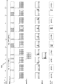
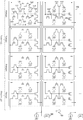
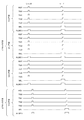
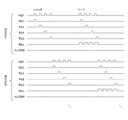
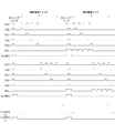
- FIG. 7 is a diagram illustrating an example of timing when reading a block row not including an ROI in the first example of pixel driving in the embodiment of the present technology.
- FIG. 13 is a diagram illustrating an example of timing when reading a block row including an ROI in the first example of pixel driving in the embodiment of the present technology. It is a figure which shows the 2nd example of the pixel drive of the imaging device in embodiment of this technique.
- FIG. 21 is a diagram illustrating an example of timing when reading a block row including an ROI in a second example of pixel driving in the embodiment of the present technology. It is a figure showing an example of the column drive division circuit of the pixel circuit assumed in the 2nd example of the pixel drive of an embodiment of this art. It is a figure showing an example of the pixel circuit assumed in the 3rd example of the pixel drive of an embodiment of this art.
- FIG. 21 is a diagram illustrating an example of timing when reading a block row including an ROI in a third example of pixel driving in the embodiment of the present technology.
- FIG. 1 is a diagram illustrating a configuration example of an imaging device according to an embodiment of the present technology.
- the imaging apparatus includes an imaging element 100, a signal processing unit 200, a system control unit 300, and a driving unit 400.
- the imaging element 100 is a pixel array in which pixels for imaging a subject are two-dimensionally arranged.
- the imaging element 100 configures a pixel array by arranging pixel rows arranged in a predetermined direction in a direction perpendicular to the predetermined direction.
- a pixel row is generally a line or line group aligned in the horizontal direction, and exposure and imaging are performed in units of this pixel row. However, exposure and imaging may be performed by arranging the pixel rows in the vertical direction.
- the imaging device 100 is driven by the drive unit 400 in accordance with control from the system control unit 300.
- the imaging device 100 performs normal imaging with high resolution for a region of interest (ROI), and performs sensing imaging with low resolution for other regions.
- ROI region of interest
- normal imaging is imaging for recording and displaying an image, etc., and imaging with high resolution such as 2560 pixels ⁇ 1440 pixels is performed.
- a high bit rate of, for example, about 10 bits is assumed in the A / D conversion with a normal dynamic range of about 60 dB.
- color imaging such as RGB is assumed, for example.
- a high frame rate of about 60 fps (frames / second) is assumed.
- sensing imaging is imaging for detecting a moving body, and imaging with low resolution such as 16 pixels ⁇ 5 pixels is performed.
- a high dynamic range of about 100 dB, and a low bit rate of about 8 bits, for example, are assumed in A / D conversion.
- a low frame rate of about 30 fps by monochrome imaging is assumed.
- imaging is performed not in units of regions but in units of pixel rows, and therefore pixel rows including the ROI are read by high resolution and then low by pixel addition. Resolution is performed.
- the signal processing unit 200 performs signal processing on the imaging signal read from the imaging element 100.
- the signal processing unit 200 includes a high resolution area image processing unit 210, a pixel addition unit 220, a low resolution area image processing unit 230, a motion detection processing unit 240, an exposure evaluation value generation unit 250, and an output processing unit 260.
- the high resolution region image processing unit 210 performs signal processing on the ROI in which the normal imaging with high resolution is performed in the imaging device 100.
- the high resolution region image processing unit 210 is an example of a first image processing unit described in the claims.
- the pixel addition unit 220 performs pixel addition on the pixel row on which the normal imaging with high resolution has been performed in the imaging device 100 to reduce the resolution.
- the result of the pixel addition unit 220 is supplied to the low resolution region image processing unit 230.
- the low resolution region image processing unit 230 performs signal processing on the imaging signal on which the sensing imaging with low resolution is performed in the imaging element 100 and the imaging signal on which the resolution is reduced by the pixel adding unit 220.
- the low resolution region image processing unit 230 is for the entire low resolution region including the imaging signal of which the sensing imaging with low resolution is performed in the imaging device 100 and the imaging signal whose resolution is reduced by the pixel addition unit 220. Perform signal processing.
- the low resolution region image processing unit 230 is an example of a second image processing unit described in the claims.
- the motion detection processing unit 240 detects motion in accordance with the time-series change of the image of the entire area subjected to the signal processing by the low resolution area image processing unit 230.
- the area in which the motion is detected by the motion detection processing unit 240 is supplied to the system control unit 300 and the exposure evaluation value generation unit 250.
- the exposure evaluation value generation unit 250 generates an exposure evaluation value (AE (Auto Exposure) evaluation value) for exposure control.
- AE Exposure
- the exposure evaluation value generation unit 250 generates an exposure evaluation value based on the area in which the motion is detected by the motion detection processing unit 240 in the image of the entire area subjected to the signal processing by the low resolution area image processing unit 230. Do.
- the exposure evaluation value generated by the exposure evaluation value generation unit 250 is supplied to the system control unit 300.
- the output processing unit 260 outputs the imaging signal of the ROI subjected to the signal processing by the high resolution region image processing unit 210 to the processing of the subsequent stage.
- the process of the latter stage for example, display control for outputting to a display device, recording control for recording on a recording medium, and the like are assumed.
- the imaging signal of the ROI is output, the imaging signal of the image of the entire region subjected to the signal processing by the low resolution region image processing unit 230 may be output.
- the system control unit 300 controls the entire imaging apparatus.
- the system control unit 300 controls, for example, high-resolution imaging of an area in which a motion is detected by the motion detection processing unit 240 as an ROI.
- the system control unit 300 also performs control to capture an image based on the exposure evaluation value generated by the exposure evaluation value generation unit 250, for example.
- the system control unit 300 is an example of a control unit described in the claims.
- the drive unit 400 drives the imaging device 100 according to control from the system control unit 300.
- FIG. 2 is a diagram illustrating a basic operation example of the imaging device according to the embodiment of the present technology.
- a moving object is detected in the subject at time T2 to T4.
- the imaging element 100 performs high-resolution pixel readout on pixel rows including the ROI, using the region in which the motion is detected by the motion detection processing unit 240 as the ROI.
- low resolution pixel readout is performed for pixel rows that do not include the ROI.
- the high resolution region image processing unit 210 performs signal processing on the ROI in which the normal imaging with the high resolution is performed in the imaging device 100, and the output processing unit 260 outputs the signal. That is, as shown by the sensor output in the figure, an output is performed for a region (ROI) in which the motion is detected during a period in which the motion is detected. Therefore, no image is output during a period in which no motion is detected.
- the imaging device 100 is an event-driven imaging device driven by an event of motion detection.
- the pixel adding unit 220 performs resolution reduction for the pixel row in which the normal imaging with high resolution is performed in the imaging element 100.
- low resolution pixel readout is performed for pixel rows that do not include the ROI.
- the image of the entire area is supplied to the low resolution area image processing unit 230 with low resolution.
- the low resolution region image processing unit 230 performs signal processing on the low resolution entire region image, and the motion detection processing unit 240 is subjected to motion detection processing. Therefore, even when a new moving object intrudes into an area other than the immediately preceding ROI, motion can be detected from the image of the entire area.
- the motion detection processing unit 240 performs moving object tracking, and follows while predicting the region in which the ROI moves in the next image (frame) of time series.
- the exposure evaluation value generation unit 250 generates an exposure evaluation value on the basis of the region (ROI) in which the movement is detected. Thereby, high resolution imaging can be performed by appropriate exposure in the ROI.
- FIG. 3 is a diagram illustrating an example of timing of pixel readout of the imaging device according to the embodiment of the present technology.
- the motion detection processing unit 240 detects this.
- sensing imaging is performed at a high frame rate to predict the movement of the moving body. That is, the frame rate is doubled from time T3 to T5. This makes it possible to accurately predict the motion of the moving body, and a high resolution normal readout 702 is performed on the ROI at time T5.
- the image of the ROI captured in this manner is output through the high resolution region image processing unit 210 and the output processing unit 260.
- the moving body is followed and an image of the ROI is output. During that time, if there is a deviation from the predicted area, the trajectory of that prediction is corrected.
- time T8 When no moving body is detected at time T8, high-resolution imaging is not performed, and the image is not output.
- FIG. 4 is a diagram illustrating an example of region prediction in the embodiment of the present technology.
- the center of gravity of a moving object is estimated.
- the center of gravity of the moving body may be, for example, the coordinates of the center of the area of the moving body, or may be the center coordinates in consideration of the weighting by the density of the luminance value.
- the center of gravity of the moving object is similarly estimated in the next frame of the time series, and the moving direction and moving speed of the moving object center of gravity are estimated from the difference.
- the center of gravity of the moving body and the area of the moving body in the next frame can be further predicted.
- FIG. 5 is a diagram illustrating another example of timing of pixel readout of the imaging device according to the embodiment of the present technology. This example shows a timing example in the case of dynamically changing the frame rate at the time of imaging with high resolution.
- the system control unit 300 controls the imaging element 100 to perform imaging at a low frame rate from time T6.
- the system control unit 300 controls the imaging element 100 to perform imaging at a high frame rate from time T8.
- the frame rate can be dynamically changed in accordance with the moving speed of the moving object.
- FIG. 6 is a diagram illustrating an operation example when a plurality of moving objects are detected in the embodiment of the present technology.
- a moving object is detected in the subject at time T2, and then another moving object is detected at time T3. That is, after time T3, a plurality of moving bodies having different moving speeds and moving directions exist in the subject.
- the imaging device 100 selects a region so that all moving objects to be targets are contained, and performs pixel readout with high resolution. Then, as indicated by the sensor output at time T3, the high resolution region image processing unit 210 cuts out the region where each moving body exists as an ROI, and outputs a plurality of regions via the output processing unit 260.
- a region including both may be cut out as an ROI.
- separate regions are cut out as ROIs as shown at time T5.
- the exposure evaluation value generation unit 250 generates an exposure evaluation value for the plurality of regions, and imaging control is performed based on the exposure evaluation values.
- FIG. 7 is a diagram illustrating an operation example when normal imaging and sensing imaging are performed on different frames in the embodiment of the present technology.
- a moving object is detected in the subject from time T3 to T11.
- time T1 and time T2 no motion is detected in the subject, so only low-resolution sensing readout 701 is performed.
- the captured image is not output.
- sensing imaging is performed at a high frame rate, as in the above-described embodiment.
- the normal readout 702 with high resolution is performed on the ROI, and an image of the ROI is output.
- the low resolution sensing readout 701 is performed on the entire image, and the image is not output.
- normal imaging and sensing imaging can be repeated without switching between normal imaging and sensing imaging for each pixel row in one frame.
- the frame rate at which the ROI is output is halved.
- FIG. 8 is a flowchart illustrating an example of determination of imaging control of each region in an image according to the embodiment of the present technology.
- the area in the image is divided into N areas # 0 to # (N-1), and the contents of imaging control are determined for each area.
- the determination is repeated for each area using the variable n.
- the initial value of the variable n is "0" (step S911).
- the imaging device 100 captures the area #n at high resolution, and the ROI of the ROI via the high resolution area image processing unit 210 and the output processing unit 260.
- An imaging signal is output (step S 913).
- the image pickup signal of the area #n imaged at high resolution is reduced in resolution by the pixel addition unit 220 (step S 914), and is supplied to the motion detection processing unit 240 via the low resolution area image processing unit 230. .
- step S915: No when the moving object is not detected in the area #n (step S915: No), the motion detection processing unit 240 determines that the movement which has been detected in the area #n up to this point is lost. The movement tracking is corrected (step S926).
- step S915: Yes when a moving object is detected in the area #n (step S915: Yes), it is determined that there is no change in the detection of the moving object, and "1" is added to the variable n (step S927). move on. That is, while the variable n is smaller than N (step S 928: Yes), the processing after step S 912 is repeated.
- the imaging element 100 captures an image of the area #n at a low resolution (step S923).
- the imaging signal of the area #n imaged at low resolution is supplied to the motion detection processing unit 240 via the low resolution area image processing unit 230.
- step S925: Yes if the motion detection processing unit 240 detects a moving object in the area #n (step S925: Yes), it determines that a new moving object has entered the area #n, and follows the movement for the next frame. Is corrected (step S926).
- step S925: No when no moving object is detected in the area #n (step S925: No), it is determined that there is no change in the detection of the moving object, "1" is added to the variable n (step S927), and processing of the next area is performed. move on. That is, while the variable n is smaller than N (step S 928: Yes), the processing after step S 912 is repeated.
- FIG. 9 is a diagram illustrating a first example of pixel driving of the imaging device according to the embodiment of the present technology.
- pixels are driven in units of block rows which are line groups aligned in the horizontal direction.
- the block row including the ROI 710 is driven by high resolution readout (high resolution imaging drive).
- block rows not including the ROI 710 are driven by low resolution readout by pixel addition (sensing imaging drive).
- FIG. 10 is a diagram illustrating an example of a pixel circuit assumed in a first example of pixel driving according to the embodiment of the present technology.
- an FD shared pixel circuit in which an FD (Floating Diffusion) 119 is shared by four pixels 111 to 114 is used.
- the four pixels 111 to 114 are photodiodes that convert received light into charge.
- the FD 119 is a diffusion layer region that converts charge into a voltage signal.
- the four pixels 111 to 114 are assigned, for example, a color of Bayer arrangement, and are configured by a red pixel, a blue pixel, and two green pixels. Lines aligned horizontally in units of four pixels 111 to 114 are referred to as FD rows. Then, N FD rows arranged in the vertical direction are referred to as block rows.
- Transfer transistors 121 to 124 are connected to each of the four pixels 111 to 114. Transfer gate signals TG0 to TG3 are supplied to the gates of the transfer transistors 121 to 124, and transfer to the FD 119 is controlled.
- the reset transistor 131 is connected to the FD 119.
- the reset signal RST is supplied to the gate of the reset transistor 131, and the reset of the pixels 111 to 114 and the FD 119 is controlled.
- the amplification transistor 132 is connected to the FD 119.
- the amplification transistor 132 amplifies a voltage signal based on the charge transferred from the pixels 111 to 114 to the FD 119.
- the selection transistor 141 is connected to the amplification transistor 132.
- a selection signal SEL is supplied to the gate of the selection transistor 141, and the output to the vertical signal line (VSL: Vertical Signal Line) 150 is controlled.
- addition transistor 151 is connected to the FD 119.
- the addition enable signal ALSEN is supplied to the gate of the addition transistor 151, whereby the addition of charges by the FD connection in the vertical direction is controlled.
- the outputs from the four pixels 111 to 114 are supplied column by column to the vertical signal line 150 and converted into digital signals by the A / D converter 180. Also, the vertical signal line 150 is selectively connected by the switch 160 so that addition can be performed in the horizontal direction. That is, in the image pickup element 100, pixel addition by FD connection in the vertical direction and pixel addition in the horizontal direction by the switch 160 can be performed at an analog level, whereby low resolution readout can be performed.
- FIG. 11 is a diagram illustrating an example of timing when reading a block row including no ROI in the first example of pixel driving in the embodiment of the present technology.
- the sensing imaging drive is applied to the block rows not including the ROI. That is, pixel addition is performed at an analog level, and low resolution readout is performed.
- the shutter operation is simultaneously performed on all the FD rows of one block row, and the exposure is started. Then, after the exposure period has elapsed, the read operation is performed simultaneously on all the FD rows of one block row.
- the addition enable signal ALSEN becomes valid (high level), and pixel addition in the vertical direction of one block row is performed. Further, the switch 160 is turned on (on), and pixel addition in the horizontal direction is performed.
- FIG. 12 is a diagram illustrating an example of timing when reading a block row including an ROI in the first example of pixel driving in the embodiment of the present technology.
- high resolution imaging driving is applied to block rows including the ROI. That is, as shown in the drawing, the transfer gate signals TG0 to TG3 become valid (high level) in the respective pixels 111 to 114 of the FD row by shifting the time, and the exposure is started. Then, after the exposure period has elapsed in each of the pixels 111 to 114, readout is performed.
- the pixel adding unit 220 of the signal processing unit 200 performs resolution reduction of the digital level.
- FIG. 13 is a diagram illustrating a second example of pixel driving of the imaging device according to the embodiment of the present technology.
- both of the sensing imaging drive and the high resolution imaging drive are performed at different times with respect to the block row including the ROI 710.
- the target drive is selected for each block row by the column enable signal CLMEN.
- the sensing imaging driving is performed as in the first example.
- FIG. 14 is a diagram illustrating an example of a pixel circuit assumed in the second example of the pixel drive according to the embodiment of the present technology.
- This pixel circuit has the same configuration as that described for the first example.
- the column enable signal CLMEN is connected to each block row consisting of pixel row groups in the vertical direction, and the drive is controlled to each block row. That is, CLMEN (0) is connected to 1 block row, CLMEN (1) is connected to 2 block row, and similarly, CLMEN (M-1) is connected to M block row, Control is performed in units of block sequences.
- FIG. 15 is a diagram illustrating an example of timing when reading a block row including an ROI in the second example of the pixel driving in the embodiment of the present technology.
- the first block row does not include the ROI
- the second block row includes the ROI. Therefore, CLMEN (0) is enabled (high level) at the timing of the sensing imaging drive. On the other hand, at the timing of the high resolution imaging drive, CLMEN (1) is made effective (high level). Thereby, the drive content to be applied can be selected for each block row.
- the timing example for reading out a block row not including the ROI is the same as that of the first example described above, and thus the detailed description will be omitted.
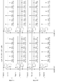
- FIG. 16 is a diagram illustrating an example of a column drive division circuit of the pixel circuit assumed in the second example of the pixel drive according to the embodiment of the present technology.
- the column drive division circuit is a circuit that generates transfer gate signals TG0 to TG3 of the FD row according to the column enable signal CLMEN.
- a transfer gate signal after division is generated by generating the logical product of the transfer gate signal of the FD row and the column enable signal.
- transfer gate signals after division are represented as TG # (block column, FD row, FD column).
- FIG. 17 is a diagram illustrating an example of a pixel circuit assumed in a third example of the pixel drive according to the embodiment of the present technology.
- the pixel arrangement in the Bayer arrangement is assumed, but in this third example, one of two green pixels is used as a pixel for sensing addition.
- the pixels for this sensing addition may be used as green pixels in the Bayer arrangement or may be white pixels without color filters.
- a pixel 115 for sensing addition is provided instead of the pixel 114.
- the transfer transistor 125 is connected to the pixel 115, and the transfer gate signal TGW is supplied to the gate of the transfer transistor 125.
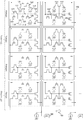
- FIG. 18 is a diagram illustrating an example of timing when reading a block row including an ROI in the third example of pixel driving in the embodiment of the present technology.
- both the sensing imaging and the high resolution imaging are performed for the block row including the ROI. That is, during sensing imaging, only the TGW is driven, and the other TGs 0 to 2 are not driven. On the other hand, at the time of high resolution imaging driving, only the other TGs 0 to 2 are driven without driving the TGW.
- pixels can be controlled independently to perform both sensing imaging and high resolution imaging.
- the timing example for reading out a block row not including the ROI is the same as that of the first example described above, and thus the detailed description will be omitted.
- the imaging device is configured to capture and output only the region of interest (ROI) at high resolution and capture the entire image at low resolution and track the ROI. Power consumption of 100 can be reduced.
- ROI region of interest
- the processing procedure described in the above embodiment may be regarded as a method having a series of these procedures, and a program for causing a computer to execute the series of procedures or a recording medium storing the program. You may catch it.
- a recording medium for example, a CD (Compact Disc), an MD (Mini Disc), a DVD (Digital Versatile Disc), a memory card, a Blu-ray disc (Blu-ray (registered trademark) Disc) or the like can be used.
- the present technology can also be configured as follows. (1) In a two-dimensional pixel array in which pixel rows arranged in a predetermined direction are arranged in a direction perpendicular to the predetermined direction, imaging with a predetermined resolution is performed for a first pixel row including a predetermined area; An imaging element for performing imaging with a resolution lower than the predetermined resolution for the second pixel row other than the pixel row of A first image processing unit that generates an image of the predetermined area based on an imaging signal of the first pixel row; A pixel addition unit that performs addition processing between pixels on the imaging signal of the first pixel row to obtain the same resolution as the imaging signal of the second pixel row; A second image processing unit configured to generate an image of the entire area based on the imaging signal of the second pixel row and the imaging signal of the first pixel row subjected to the addition processing.
- the image pickup apparatus further comprising: a control unit configured to control the image pickup device to pick up the first pixel row with the region where the movement is detected as the predetermined region.
- a control unit configured to control the image pickup device to pick up the first pixel row with the region where the movement is detected as the predetermined region.
- the control unit controls the imaging element to increase a frame rate when transitioning from a state in which the movement is not detected to a state in which the movement is detected .
- the control unit controls the imaging element to change a frame rate in accordance with a moving speed of the region in which the movement is detected.
- the control unit is configured to capture the first pixel row with the area including the moving bodies as the predetermined area.
- the imaging device according to any one of (2) to (4), which controls an imaging element.
- the apparatus further comprises an exposure evaluation value generation unit that generates an exposure evaluation value on the basis of the area where the movement is detected in the image of the entire area.
- the imaging apparatus according to any one of (2) to (5), wherein the control unit controls the imaging element to perform exposure based on the exposure evaluation value.
- the imaging element In the state in which the movement is detected, the imaging element performs imaging with the predetermined resolution for the first pixel row and does not perform imaging for the second pixel row.
- the imaging device according to any one of (2) to (6), wherein a frame period and a second frame period in which imaging with a resolution lower than the predetermined resolution is performed for all pixel rows are alternately repeated.
- the imaging device according to any one of (2) to (7), wherein the imaging element performs imaging with the predetermined resolution on the first pixel row only when the movement is detected.
- the imaging apparatus according to any one of (1) to (8), further including an output processing unit that outputs the image of the predetermined area generated by the first image processing unit.
- imaging with a predetermined resolution is performed for a first pixel row including a predetermined area;
- An imaging element for performing imaging with a resolution lower than the predetermined resolution for the second pixel row other than the pixel row of A first image processing procedure for generating an image of the predetermined area based on an imaging signal of the first pixel row;
- Control of an imaging element comprising a second image processing procedure for generating an image of the entire area based on the imaging signal of the second pixel row and the imaging signal of the first pixel row subjected to the addition processing Method.
Landscapes
- Engineering & Computer Science (AREA)
- Multimedia (AREA)
- Signal Processing (AREA)
- Transforming Light Signals Into Electric Signals (AREA)
- Studio Devices (AREA)
Abstract
関心領域(ROI)のみを高解像度で出力する撮像素子の消費電力を低減する。 撮像素子は、所定方向に配置された画素行を所定方向の垂直方向に配置した2次元の画素アレイにおいて、所定の領域を含む第1の画素行については高解像度による撮像を行い、それ以外の第2の画素行については低解像度による撮像を行う。第1の画像処理部は、第1の画素行の撮像信号に基づいて所定の領域の画像を生成する。画素加算部は、第1の画素行の撮像信号について画素間の加算処理を施して、第2の画素行の撮像信号と同じ解像度にする。第2の画像処理部は、第2の画素行の撮像信号および加算処理が施された第1の画素行の撮像信号に基づいて全領域の画像を生成する。
Description
本技術は、撮像装置に関する。詳しくは、画像を撮像する撮像素子を備える撮像装置およびその撮像素子の制御方法に関する。
画像処理等を行う際、画像内の特定の領域に着目して処理が行われることがある。この場合の領域は関心領域(ROI:Region Of Interest)と呼ばれる。撮像装置において、このような特定の領域に絞って撮像を行えば消費電力を低減することが期待される。そのため、例えば、第1の撮像部で得られた第1の画像において注目被写体領域を判別し、その注目被写体領域に応じて第2の撮像部を制御して、第2の画像を得る撮像装置が提案されている(例えば、特許文献1参照。)。
上述の従来技術では、注目被写体領域に応じて画像を撮像するよう制御を行っていた。しかしながら、注目被写体領域を判別する第1の画像の撮像と注目被写体領域に応じた第2の画像の撮像とを分けて行うため、消費電力を十分に低減することができなくなるおそれがある。
本技術はこのような状況に鑑みて生み出されたものであり、関心領域のみを高解像度で出力する撮像素子の消費電力を低減することを目的とする。
本技術は、上述の問題点を解消するためになされたものであり、その第1の側面は、所定方向に配置された画素行を上記所定方向の垂直方向に配置した2次元の画素アレイにおいて所定の領域を含む第1の画素行については所定の解像度による撮像を行い、上記第1の画素行以外の第2の画素行については上記所定の解像度よりも低い解像度による撮像を行う撮像素子と、上記第1の画素行の撮像信号に基づいて上記所定の領域の画像を生成する第1の画像処理部と、上記第1の画素行の撮像信号について画素間の加算処理を施して上記第2の画素行の撮像信号と同じ解像度にする画素加算部と、上記第2の画素行の撮像信号および上記加算処理が施された上記第1の画素行の撮像信号に基づいて全領域の画像を生成する第2の画像処理部とを具備する撮像装置および撮像素子の制御方法である。これにより、所定の領域のみを高解像度で撮像して出力し、全領域の画像については低高解像度で撮像することにより、撮像素子の消費電力を低減するという作用をもたらす。
また、この第1の側面において、上記全領域の画像の時系列の変化に従って動きを検出する動き検出処理部と、上記動きが検出されている領域を上記所定の領域として上記第1の画素行を撮像するよう上記撮像素子を制御する制御部とをさらに具備してもよい。これにより、低高解像度で撮像した全領域の画像において動きを検出して所定の領域として追従させるという作用をもたらす。
また、この第1の側面において、上記制御部は、上記動きが検出されていない状態から上記動きが検出されている状態に遷移したときにフレームレートを上げるよう上記撮像素子を制御するようにしてもよい。これにより、フレームレートを上げて領域予測をさせるという作用をもたらす。
また、この第1の側面において、上記制御部は、上記動きが検出されている領域の移動速度に応じてフレームレートを変化させるよう上記撮像素子を制御するようにしてもよい。これにより、移動速度に応じてフレームレートをダイナミックに変化させるという作用をもたらす。
また、この第1の側面において、上記制御部は、上記全領域の画像において移動速度の異なる動体が複数検出された場合にはそれら動体を包含する領域を上記所定の領域として上記第1の画素行を撮像するよう上記撮像素子を制御するようにしてもよい。これにより、複数の動体をまとめて取り扱うという作用をもたらす。
また、この第1の側面において、上記全領域の画像において上記動きが検出されている領域を基準として露光評価値を生成する露光評価値生成部をさらに具備し、上記制御部は、上記露光評価値に基づいて露光を行うよう上記撮像素子を制御するようにしてもよい。これにより、動きが検出されている領域を基準として露光を行うという作用をもたらす。
また、この第1の側面において、上記撮像素子は、上記動きが検出されている状態においては、上記第1の画素行について上記所定の解像度による撮像を行うとともに上記第2の画素行については撮像を行わない第1のフレーム期間と、全ての画素行について上記所定の解像度よりも低い解像度による撮像を行う第2のフレーム期間とを交互に繰り返すようにしてもよい。これにより、フレーム期間毎に画素行の制御を共通化するという作用をもたらす。
また、この第1の側面において、上記撮像素子は、上記動きが検出されている状態においてのみ上記第1の画素行について上記所定の解像度による撮像を行うようにしてもよい。これにより、動き検出というイベントにより駆動するという作用をもたらす。
また、この第1の側面において、上記第1の画像処理部によって生成された上記所定の領域の画像を出力する出力処理部をさらに具備してもよい。これにより、所定の領域の画像のみを出力するという作用をもたらす。
本技術によれば、関心領域のみを高解像度で出力する撮像素子の消費電力を低減することができるという優れた効果を奏し得る。なお、ここに記載された効果は必ずしも限定されるものではなく、本開示中に記載されたいずれかの効果であってもよい。
以下、本技術を実施するための形態(以下、実施の形態と称する)について説明する。説明は以下の順序により行う。
1.構成(撮像装置の構成例)
2.動作(撮像装置の動作例)
3.回路(画素駆動の実装例)
1.構成(撮像装置の構成例)
2.動作(撮像装置の動作例)
3.回路(画素駆動の実装例)
<1.構成>
[撮像装置の構成]
図1は、本技術の実施の形態における撮像装置の構成例を示す図である。この撮像装置は、撮像素子100と、信号処理部200と、システム制御部300と、駆動部400とを備える。
[撮像装置の構成]
図1は、本技術の実施の形態における撮像装置の構成例を示す図である。この撮像装置は、撮像素子100と、信号処理部200と、システム制御部300と、駆動部400とを備える。
撮像素子100は、被写体を撮像する画素を2次元に配置した画素アレイである。この撮像素子100は、所定方向に配置された画素行を、所定方向の垂直方向に配置することにより画素アレイを構成する。画素行は、一般に水平方向に並ぶラインまたはライン群であり、この画素行を単位として露光および撮像が行われる。ただし、この画素行を垂直方向に並べて露光および撮像を行うようにしてもよい。
この撮像素子100は、システム制御部300からの制御に従って、駆動部400によって駆動される。この撮像素子100は、関心領域(ROI)については高解像度による通常撮像を行い、他の領域については低解像度によるセンシング撮像を行う。
ここで、通常撮像は、画像を記録および表示等するための撮像であり、例えば2560画素×1440画素などの高解像度による撮像を行うものである。この通常撮像では、60dB程度の通常のダイナミックレンジで、A/D変換の際には例えば10ビット程度の高いビットレートが想定される。また、例えばRGB等のカラー撮像が想定される。また、60fps(フレーム/秒)程度の高フレームレートが想定される。
一方、センシング撮像は、動体を検出するための撮像であり、例えば16画素×5画素などの低解像度による撮像を行うものである。このセンシング撮像では、100dB程度の高いダイナミックレンジで、A/D変換の際には例えば8ビット程度の低いビットレートが想定される。また、モノクロ撮像による、30fps程度の低フレームレートが想定される。
なお、後述するように、撮像素子100においては、領域を単位とするのではなく、画素行を単位として撮像が行われるため、ROIを含む画素行については高解像度により読み出した後に画素加算による低解像度化が行われる。
信号処理部200は、撮像素子100から読み出された撮像信号に対して信号処理を施すものである。この信号処理部200は、高解像度領域画像処理部210と、画素加算部220と、低解像度領域画像処理部230と、動き検出処理部240と、露光評価値生成部250と、出力処理部260とを備える。
高解像度領域画像処理部210は、撮像素子100において高解像度による通常撮像が行われたROIについて信号処理を行うものである。なお、高解像度領域画像処理部210は、特許請求の範囲に記載の第1の画像処理部の一例である。
画素加算部220は、撮像素子100において高解像度による通常撮像が行われた画素行について、画素加算を行って低解像度化するものである。この画素加算部220による結果は、低解像度領域画像処理部230に供給される。
低解像度領域画像処理部230は、撮像素子100において低解像度によるセンシング撮像が行われた撮像信号および画素加算部220によって低解像度化された撮像信号について信号処理を行うものである。この低解像度領域画像処理部230は、撮像素子100において低解像度によるセンシング撮像が行われた撮像信号と、画素加算部220によって低解像度化された撮像信号とを併せた、低解像度の全領域について信号処理を行う。なお、低解像度領域画像処理部230は、特許請求の範囲に記載の第2の画像処理部の一例である。
動き検出処理部240は、低解像度領域画像処理部230により信号処理が施された全領域の画像の時系列の変化に従って、動きを検出するものである。この動き検出処理部240によって動きが検出された領域は、システム制御部300および露光評価値生成部250に供給される。
露光評価値生成部250は、露光制御のための露光評価値(AE(Auto Exposure) 評価値)を生成するものである。この露光評価値生成部250は、低解像度領域画像処理部230により信号処理が施された全領域の画像において、動き検出処理部240によって動きが検出されている領域を基準として露光評価値を生成する。この露光評価値生成部250によって生成された露光評価値は、システム制御部300に供給される。
出力処理部260は、高解像度領域画像処理部210によって信号処理が施されたROIの撮像信号を後段の処理に出力するものである。ここで、後段の処理としては、例えば、表示装置に出力するための表示制御や、記録媒体に記録するための記録制御などが想定される。なお、ここではROIの撮像信号を出力することを想定したが、低解像度領域画像処理部230によって信号処理が施された全領域の画像の撮像信号を出力するようにしてもよい。
システム制御部300は、撮像装置全体を制御するものである。このシステム制御部300は、例えば、動き検出処理部240によって動きが検出されている領域をROIとして高解像度により撮像するよう制御する。また、このシステム制御部300は、例えば、露光評価値生成部250によって生成された露光評価値に基づいて撮像するよう制御する。なお、システム制御部300は、特許請求の範囲に記載の制御部の一例である。
駆動部400は、システム制御部300からの制御に従って撮像素子100を駆動するものである。
<2.動作>
[基本的な動作]
図2は、本技術の実施の形態における撮像装置の基本的な動作例を示す図である。
[基本的な動作]
図2は、本技術の実施の形態における撮像装置の基本的な動作例を示す図である。
この例では、時刻T2からT4において、被写体中に動体が検出される。撮像素子100は、動き検出処理部240によって動きが検出されている領域をROIとして、ROIを含む画素行について高解像度による画素読出しを行う。一方、ROIを含まない画素行については低解像度による画素読出しを行う。
撮像素子100において高解像度による通常撮像が行われたROIについて高解像度領域画像処理部210が信号処理を行い、出力処理部260が出力する。すなわち、同図におけるセンサ出力が示すように、動きが検出されている期間に、動きが検出されている領域(ROI)について出力が行われる。したがって、動きが検出されていない期間においては、画像は出力されない。換言すれば、撮像素子100は、動き検出というイベントによって駆動されるイベントドリブンの撮像素子である。
撮像素子100において高解像度による通常撮像が行われた画素行については画素加算部220による低解像度化が行われる。また、ROIを含まない画素行については低解像度による画素読出しが行われる。これにより、低解像度領域画像処理部230には、全領域の画像が低解像度により供給される。この低解像度の全領域の画像は、低解像度領域画像処理部230によって信号処理が行われ、動き検出処理部240による動き検出の処理対象となる。そのため、直前のROI以外の領域に新たな動体が侵入した場合でも、全領域の画像から動きを検出することができる。また、動き検出処理部240は、一旦動きを検出した後は動体追跡を行い、時系列の次画像(フレーム)においてROIが移動する領域を予測しながら追従していく。
また、露光評価値生成部250は、動きが検出されている領域(ROI)を基準として露光評価値を生成する。これにより、ROIにおいて適切な露光により、高解像度の撮像を行うことができる。
[動体検出直後のフレームレート]
図3は、本技術の実施の形態における撮像装置の画素読出しのタイミング例を示す図である。
図3は、本技術の実施の形態における撮像装置の画素読出しのタイミング例を示す図である。
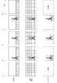
この例では、時刻T3からT7において、被写体中に動体が検出される。時刻T1および時刻T2においては、被写体中に動きが検出されないため、低解像度によるセンシング読出し701のみが行われる。このとき、撮像された画像は出力されない。
時刻T3において動体(人物)が侵入すると、動き検出処理部240は、これを検出する。動体が検出されると、動体の動きを予測するため、高フレームレートによりセンシング撮像が行われる。すなわち、時刻T3からT5の間は、フレームレートが倍速になっている。これにより、動体の動きを正確に予測することが可能となり、時刻T5においてROIについて高解像度による通常読出し702が行われる。このようにして撮像されたROIの画像は、高解像度領域画像処理部210および出力処理部260を介して出力される。
その後、動体が追従されて、ROIの画像が出力されていく。その間、予測した領域とずれが生じた場合には、その予測の軌道を修正する。時刻T8において動体が検出されなくなると、高解像度による撮像は行われなくなり、画像は出力されなくなる。
図4は、本技術の実施の形態における領域予測の例を示す図である。
動体を追従する際には領域の移動方向および移動速度を予測する必要がある。この予測を行うための手法の一例として、まず、動体の重心を推定する。この動体の重心は、例えば、動体の領域の中央の座標としてもよく、また、輝度値の濃度による重み付けを考慮した中心座標としてもよい。
時系列の次のフレームにおいて同様に動体の重心が推定され、その差分から動体重心の移動方向および移動速度が推定される。これにより、さらにその次のフレームにおける動体の重心および動体の領域を予測することができる。
上述の例では、時刻T3において動体の侵入が検出されると、時刻T3およびT4における動体の重心に基づいて、時刻T5における動体の重心および動体の領域が予測される。上述のように、時刻T3からT5の間は、フレームレートを倍速にして撮像を行うため、速やかに動体の追従を行うことができる。
[動体の移動速度とフレームレート]
図5は、本技術の実施の形態における撮像装置の画素読出しの他のタイミング例を示す図である。この例では、高解像度による撮像時のフレームレートをダイナミックに変更する場合のタイミング例を示している。
図5は、本技術の実施の形態における撮像装置の画素読出しの他のタイミング例を示す図である。この例では、高解像度による撮像時のフレームレートをダイナミックに変更する場合のタイミング例を示している。
上述の例と同様に、時刻T3において動体が検出されると、動体の動きを予測するため、高フレームレートによりセンシング撮像が行われる。その後、その動体の移動速度が低速であると判断されると、システム制御部300は、時刻T6から低フレームレートによる撮像を行うよう撮像素子100を制御する。
その後、時刻T7において新たな動体が検出されると、再び、動体の動きを予測するため、高フレームレートによりセンシング撮像が行われる。そして、その新たな動体の移動速度が高速であると判断されると、システム制御部300は、時刻T8から高フレームレートによる撮像を行うよう撮像素子100を制御する。このようにして、動体の移動速度に合わせて、フレームレートをダイナミックに変更することができる。
[複数の動体が検出された場合]
図6は、本技術の実施の形態において複数の動体が検出された場合の動作例を示す図である。
図6は、本技術の実施の形態において複数の動体が検出された場合の動作例を示す図である。
この例では、時刻T2において被写体中に動体が検出され、その後、時刻T3において別の動体が検出される。すなわち、時刻T3以降は、それぞれ移動速度および移動方向の異なる複数の動体が被写体中に存在する。
このような場合、撮像素子100は、対象となる動体が全て収まるように領域を選択して、高解像度による画素読出しを行う。そして、高解像度領域画像処理部210は、時刻T3のセンサ出力に示すように、それぞれの動体が存在する領域をROIとして切り出して、出力処理部260を介して複数の領域を出力する。
ただし、時刻T4に示すように、複数の領域が互いに重なる場合においては、両者を包含する領域をROIとして切り出してもよい。その後、複数の領域間で重なりがなくなると、時刻T5に示すように、別々の領域がROIとして切り出される。
なお、このように複数の領域をROIとした場合においても、これら複数の領域について露光評価値生成部250が露光評価値を生成して、その露光評価値に基づいて撮像の制御が行われる。
[通常撮像とセンシング撮像を異なるフレームについて行う変形例]
図7は、本技術の実施の形態において通常撮像とセンシング撮像を異なるフレームについて行う場合の動作例を示す図である。
図7は、本技術の実施の形態において通常撮像とセンシング撮像を異なるフレームについて行う場合の動作例を示す図である。
上述の実施の形態においては、1つのフレームにおいて通常撮像とセンシング撮像を画素行毎に切り替えていたが、ここではそのような切替えを行わない変形例について説明する。
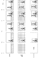
この変形例では、時刻T3からT11において、被写体中に動体が検出される。時刻T1および時刻T2においては、被写体中に動きが検出されないため、低解像度によるセンシング読出し701のみが行われる。このとき、撮像された画像は出力されない。その後、時刻T3において動体が侵入すると、高フレームレートによりセンシング撮像が行われる点は、上述の実施の形態と同様である。
この変形例では、1つのフレームにおいては通常撮像とセンシング撮像の何れか一方のみが行われる。すなわち、時刻T6においてはROIについて高解像度による通常読出し702が行われ、そのROIの画像が高解像度領域画像処理部210および出力処理部260を介して出力される。続く時刻T7においては、画像全体について低解像度によるセンシング読出し701が行われる。このとき、時刻T7の画像は出力されない。
以降は同様に、時刻T8においてはROIについて高解像度による通常読出し702が行われ、そのROIの画像が出力される。続く時刻T9においては、画像全体について低解像度によるセンシング読出し701が行われ、その画像は出力されない。
この変形例の動作によれば、1つのフレームにおいて通常撮像とセンシング撮像を画素行毎に切り替えることなく、通常撮像とセンシング撮像を繰り返すことができる。ただし、ROIが出力されるフレームレートは半分になる。
[領域毎の撮像制御]
図8は、本技術の実施の形態における画像内の各領域の撮像制御の判断例を示す流れ図である。
図8は、本技術の実施の形態における画像内の各領域の撮像制御の判断例を示す流れ図である。
この例では、画像内の領域を領域#0から領域#(N-1)のN個に分けて、各領域について撮像制御の内容を判断する。ここでは、変数nを用いて、各領域について判断を繰り返す。変数nの初期値は「0」である(ステップS911)。
領域#nにおいて動体の存在が予想されると(ステップS912:Yes)、撮像素子100は領域#nを高解像度で撮像し、高解像度領域画像処理部210および出力処理部260を介してROIの撮像信号が出力される(ステップS913)。また、高解像度で撮像された領域#nの撮像信号は、画素加算部220によって低解像度化されて(ステップS914)、低解像度領域画像処理部230を介して動き検出処理部240に供給される。
このとき、動き検出処理部240は、領域#nにおいて動体を検出しない場合(ステップS915:No)、これまで領域#nにおいて検出されていた動きがなくなったものと判断し、次のフレームのために動きの追従を修正する(ステップS926)。一方、領域#nにおいて動体を検出した場合(ステップS915:Yes)、動体の検出に変化はないと判断し、変数nに「1」を加算して(ステップS927)、次の領域の処理に進む。すなわち、変数nがNより小さい間は(ステップS928:Yes)、ステップS912以降の処理を繰り返す。
領域#nにおいて動体の存在が予想されない場合(ステップS912:No)、撮像素子100は領域#nを低解像度で撮像する(ステップS923)。低解像度で撮像された領域#nの撮像信号は、低解像度領域画像処理部230を介して動き検出処理部240に供給される。
このとき、動き検出処理部240は、領域#nにおいて動体を検出した場合(ステップS925:Yes)、領域#nに新たな動体が侵入したものと判断し、次のフレームのために動きの追従を修正する(ステップS926)。一方、領域#nにおいて動体を検出しない場合(ステップS925:No)、動体の検出に変化はないと判断し、変数nに「1」を加算して(ステップS927)、次の領域の処理に進む。すなわち、変数nがNより小さい間は(ステップS928:Yes)、ステップS912以降の処理を繰り返す。
なお、ここでは、領域毎に撮像制御の内容を判断する手順について説明したが、実際の回路においては、画素行を単位として露光および撮像が行われる。その詳細については、以下に説明する。
<3.回路>
[画素駆動の第1の例]
図9は、本技術の実施の形態における撮像装置の画素駆動の第1の例を示す図である。
[画素駆動の第1の例]
図9は、本技術の実施の形態における撮像装置の画素駆動の第1の例を示す図である。
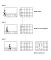
この画素駆動の第1の例では、水平方向に並ぶライン群であるブロック行を単位として画素を駆動する。その際、ROI710を含むブロック行は、高解像度読出しにより駆動される(高解像度撮影駆動)。一方、ROI710を含まないブロック行は、画素加算により、低解像度読出しにより駆動される(センシング撮影駆動)。
図10は、本技術の実施の形態の画素駆動の第1の例において想定する画素回路の一例を示す図である。
ここでは、4つの画素111乃至114によってFD(Floating Diffusion)119を共有したFD共有型の画素回路を想定している。4つの画素111乃至114は、受けた光を電荷に変換するフォトダイオードである。FD119は、電荷を電圧信号に変換する拡散層領域である。
4つの画素111乃至114は、例えばベイヤー配列の色が割り当てられ、赤画素、青画素、2つの緑画素により構成される。4つの画素111乃至114を単位として、水平方向に並ぶラインをFD行と呼称する。そして、FD行を垂直方向にN個配置したものをブロック行と呼称する。
4つの画素111乃至114の各々には、転送トランジスタ121乃至124が接続される。この転送トランジスタ121乃至124のゲートには転送ゲート信号TG0乃至TG3が供給され、FD119への転送が制御される。
また、FD119には、リセットトランジスタ131が接続される。このリセットトランジスタ131のゲートには、リセット信号RSTが供給され、画素111乃至114およびFD119のリセットが制御される。
また、FD119には、増幅トランジスタ132が接続される。この増幅トランジスタ132は、画素111乃至114からFD119に転送された電荷に基づく電圧信号を増幅するものである。この増幅トランジスタ132には選択トランジスタ141が接続される。この選択トランジスタ141のゲートには選択信号SELが供給され、垂直信号線(VSL:Vertical Signal Line)150への出力が制御される。
また、FD119には、加算トランジスタ151が接続される。この加算トランジスタ151のゲートには、加算有効信号ALSENが供給され、これにより、垂直方向のFD接続による電荷の加算が制御される。
4つの画素111乃至114からの出力は列毎に垂直信号線150に供給され、A/D変換器180によってデジタル信号に変換される。また、垂直信号線150は、スイッチ160により選択的に接続され、水平方向に加算を行うことができるようになっている。すなわち、この撮像素子100において、垂直方向のFD接続による画素加算と、スイッチ160による水平方向の画素加算とをアナログレベルで行うことができ、これにより低解像度の読出しを行うことができる。
図11は、本技術の実施の形態における画素駆動の第1の例において、ROIを含まないブロック行を読み出す際のタイミング例を示す図である。
この画素駆動の第1の例では、ROIを含まないブロック行については、センシング撮影駆動が適用される。すなわち、アナログレベルで画素加算が行われ、低解像度読出しが行われる。
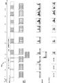
同図に示すように、1つのブロック行の全てのFD行において同時にシャッタ動作が行われ、露光が開始される。そして、露光期間経過後に、1つのブロック行の全てのFD行において同時にリード動作が行われる。このとき、加算有効信号ALSENが有効(ハイレベル)になり、1つのブロック行の垂直方向の画素加算が行われる。また、スイッチ160が導通(オン)状態になり、水平方向の画素加算が行われる。
図12は、本技術の実施の形態における画素駆動の第1の例において、ROIを含むブロック行を読み出す際のタイミング例を示す図である。
この画素駆動の第1の例では、ROIを含むブロック行については、高解像度撮影駆動が適用される。すなわち、同図に示すように、FD行のそれぞれの画素111乃至114において時間をずらして転送ゲート信号TG0乃至TG3が有効(ハイレベル)になり、露光が開始される。そして、それぞれの画素111乃至114において露光期間経過後に、読出しが行われる。
この高解像度撮影駆動においては、センシング撮影駆動のような画素加算は行われない。したがって、動き検出処理部240のために低解像度による画像を生成するために、信号処理部200の画素加算部220によってデジタルレベルの低解像度化を行う。
[画素駆動の第2の例]
図13は、本技術の実施の形態における撮像装置の画素駆動の第2の例を示す図である。
図13は、本技術の実施の形態における撮像装置の画素駆動の第2の例を示す図である。
この画素駆動の第2の例では、ROI710を含むブロック行については、時間違いでセンシング撮影駆動と高解像度撮影駆動の両方を行う。その際、カラムイネーブル信号CLMENにより、ブロック列毎に対象となる駆動を選択する。また、一方、ROI710を含まないブロック行については、第1の例と同様に、センシング撮影駆動を行う。
図14は、本技術の実施の形態の画素駆動の第2の例において想定する画素回路の一例を示す図である。
この画素回路は、第1の例について説明したものと同様の構成を備える。ただし、垂直方向の画素列群からなるブロック列毎にカラムイネーブル信号CLMENが接続され、ブロック列毎に駆動が制御される。すなわち、1ブロック列目にはCLMEN(0)が接続され、2ブロック列目にはCLMEN(1)が接続され、同様に、Mブロック列目にはCLMEN(M-1)が接続されて、ブロック列を単位とした制御が行われる。
図15は、本技術の実施の形態における画素駆動の第2の例において、ROIを含むブロック行を読み出す際のタイミング例を示す図である。
ここでは、1ブロック列目がROIを含まず、2ブロック列目がROIを含む場合を想定している。そのため、センシング撮影駆動のタイミングでは、CLMEN(0)を有効(ハイレベル)にする。一方、高解像度撮影駆動のタイミングでは、CLMEN(1)を有効(ハイレベル)にする。これにより、適用される駆動内容をブロック列毎に選択することができる。
なお、ROIを含まないブロック行を読み出す際のタイミング例については、上述の第1の例と同様であるため、詳細な説明は省略する。
図16は、本技術の実施の形態の画素駆動の第2の例において想定する画素回路の列駆動分割回路の一例を示す図である。
この列駆動分割回路は、カラムイネーブル信号CLMENに応じてFD行の転送ゲート信号TG0乃至TG3を生成する回路である。FD行の転送ゲート信号とカラムイネーブル信号との論理積を生成することにより、分割後の転送ゲート信号が生成される。ここでは、分割後の転送ゲート信号をTG#(ブロック列,FD行,FD列)として表している。
[画素駆動の第3の例]
図17は、本技術の実施の形態の画素駆動の第3の例において想定する画素回路の一例を示す図である。
図17は、本技術の実施の形態の画素駆動の第3の例において想定する画素回路の一例を示す図である。
上述の第1の例では、ベイヤー配列の画素配置を想定していたが、この第3の例では、2つの緑画素のうちの1つをセンシング加算のための画素として用いる。このセンシング加算のための画素は、ベイヤー配列における緑画素のまま使用してもよく、また、カラーフィルタ無しの白画素にしてもよい。この例では、画素114に代えてセンシング加算のための画素115を設けている。また、この画素115には転送トランジスタ125を接続し、この転送トランジスタ125のゲートには転送ゲート信号TGWを供給している。
図18は、本技術の実施の形態における画素駆動の第3の例において、ROIを含むブロック行を読み出す際のタイミング例を示す図である。
この画素駆動の第3の例では、ROIを含むブロック行については、センシング撮影と高解像度撮影の両者が行われる。すなわち、センシング撮影時にはTGWのみを駆動し、他のTG0乃至2を駆動しない。一方、高解像度撮影駆動時には、TGWを駆動せずに、他のTG0乃至2のみを駆動する。これにより、画素を独立に制御して、センシング撮影と高解像度撮影の両者を行うことができる。
なお、ROIを含まないブロック行を読み出す際のタイミング例については、上述の第1の例と同様であるため、詳細な説明は省略する。
[効果]
このように、本技術の実施の形態によれば、関心領域(ROI)のみを高解像度で撮影して出力し、全体画像については低高解像度で撮影してROIを追尾することにより、撮像素子100の消費電力を低減することができる。
このように、本技術の実施の形態によれば、関心領域(ROI)のみを高解像度で撮影して出力し、全体画像については低高解像度で撮影してROIを追尾することにより、撮像素子100の消費電力を低減することができる。
なお、上述の実施の形態は本技術を具現化するための一例を示したものであり、実施の形態における事項と、特許請求の範囲における発明特定事項とはそれぞれ対応関係を有する。同様に、特許請求の範囲における発明特定事項と、これと同一名称を付した本技術の実施の形態における事項とはそれぞれ対応関係を有する。ただし、本技術は実施の形態に限定されるものではなく、その要旨を逸脱しない範囲において実施の形態に種々の変形を施すことにより具現化することができる。
また、上述の実施の形態において説明した処理手順は、これら一連の手順を有する方法として捉えてもよく、また、これら一連の手順をコンピュータに実行させるためのプログラム乃至そのプログラムを記憶する記録媒体として捉えてもよい。この記録媒体として、例えば、CD(Compact Disc)、MD(MiniDisc)、DVD(Digital Versatile Disc)、メモリカード、ブルーレイディスク(Blu-ray(登録商標)Disc)等を用いることができる。
なお、本明細書に記載された効果はあくまで例示であって、限定されるものではなく、また、他の効果があってもよい。
なお、本技術は以下のような構成もとることができる。
(1)所定方向に配置された画素行を前記所定方向の垂直方向に配置した2次元の画素アレイにおいて所定の領域を含む第1の画素行については所定の解像度による撮像を行い、前記第1の画素行以外の第2の画素行については前記所定の解像度よりも低い解像度による撮像を行う撮像素子と、
前記第1の画素行の撮像信号に基づいて前記所定の領域の画像を生成する第1の画像処理部と、
前記第1の画素行の撮像信号について画素間の加算処理を施して前記第2の画素行の撮像信号と同じ解像度にする画素加算部と、
前記第2の画素行の撮像信号および前記加算処理が施された前記第1の画素行の撮像信号に基づいて全領域の画像を生成する第2の画像処理部と
を具備する撮像装置。
(2)前記全領域の画像の時系列の変化に従って動きを検出する動き検出処理部と、
前記動きが検出されている領域を前記所定の領域として前記第1の画素行を撮像するよう前記撮像素子を制御する制御部と
をさらに具備する前記(1)に記載の撮像装置。
(3)前記制御部は、前記動きが検出されていない状態から前記動きが検出されている状態に遷移したときにフレームレートを上げるよう前記撮像素子を制御する
前記(2)に記載の撮像装置。
(4)前記制御部は、前記動きが検出されている領域の移動速度に応じてフレームレートを変化させるよう前記撮像素子を制御する
前記(2)または(3)に記載の撮像装置。
(5)前記制御部は、前記全領域の画像において移動速度の異なる動体が複数検出された場合にはそれら動体を包含する領域を前記所定の領域として前記第1の画素行を撮像するよう前記撮像素子を制御する
前記(2)から(4)のいずれかに記載の撮像装置。
(6)前記全領域の画像において前記動きが検出されている領域を基準として露光評価値を生成する露光評価値生成部をさらに具備し、
前記制御部は、前記露光評価値に基づいて露光を行うよう前記撮像素子を制御する
前記(2)から(5)のいずれかに記載の撮像装置。
(7)前記撮像素子は、前記動きが検出されている状態においては、前記第1の画素行について前記所定の解像度による撮像を行うとともに前記第2の画素行については撮像を行わない第1のフレーム期間と、全ての画素行について前記所定の解像度よりも低い解像度による撮像を行う第2のフレーム期間とを交互に繰り返す
前記(2)から(6)のいずれかに記載の撮像装置。
(8)前記撮像素子は、前記動きが検出されている状態においてのみ前記第1の画素行について前記所定の解像度による撮像を行う
前記(2)から(7)のいずれかに記載の撮像装置。
(9)前記第1の画像処理部によって生成された前記所定の領域の画像を出力する出力処理部をさらに具備する前記(1)から(8)のいずれかに記載の撮像装置。
(10)所定方向に配置された画素行を前記所定方向の垂直方向に配置した2次元の画素アレイにおいて所定の領域を含む第1の画素行については所定の解像度による撮像を行い、前記第1の画素行以外の第2の画素行については前記所定の解像度よりも低い解像度による撮像を行う撮像素子において、
前記第1の画素行の撮像信号に基づいて前記所定の領域の画像を生成する第1の画像処理手順と、
前記第1の画素行の撮像信号について画素間の加算処理を施して前記第2の画素行の撮像信号と同じ解像度にする画素加算手順と、
前記第2の画素行の撮像信号および前記加算処理が施された前記第1の画素行の撮像信号に基づいて全領域の画像を生成する第2の画像処理手順と
を具備する撮像素子の制御方法。
(1)所定方向に配置された画素行を前記所定方向の垂直方向に配置した2次元の画素アレイにおいて所定の領域を含む第1の画素行については所定の解像度による撮像を行い、前記第1の画素行以外の第2の画素行については前記所定の解像度よりも低い解像度による撮像を行う撮像素子と、
前記第1の画素行の撮像信号に基づいて前記所定の領域の画像を生成する第1の画像処理部と、
前記第1の画素行の撮像信号について画素間の加算処理を施して前記第2の画素行の撮像信号と同じ解像度にする画素加算部と、
前記第2の画素行の撮像信号および前記加算処理が施された前記第1の画素行の撮像信号に基づいて全領域の画像を生成する第2の画像処理部と
を具備する撮像装置。
(2)前記全領域の画像の時系列の変化に従って動きを検出する動き検出処理部と、
前記動きが検出されている領域を前記所定の領域として前記第1の画素行を撮像するよう前記撮像素子を制御する制御部と
をさらに具備する前記(1)に記載の撮像装置。
(3)前記制御部は、前記動きが検出されていない状態から前記動きが検出されている状態に遷移したときにフレームレートを上げるよう前記撮像素子を制御する
前記(2)に記載の撮像装置。
(4)前記制御部は、前記動きが検出されている領域の移動速度に応じてフレームレートを変化させるよう前記撮像素子を制御する
前記(2)または(3)に記載の撮像装置。
(5)前記制御部は、前記全領域の画像において移動速度の異なる動体が複数検出された場合にはそれら動体を包含する領域を前記所定の領域として前記第1の画素行を撮像するよう前記撮像素子を制御する
前記(2)から(4)のいずれかに記載の撮像装置。
(6)前記全領域の画像において前記動きが検出されている領域を基準として露光評価値を生成する露光評価値生成部をさらに具備し、
前記制御部は、前記露光評価値に基づいて露光を行うよう前記撮像素子を制御する
前記(2)から(5)のいずれかに記載の撮像装置。
(7)前記撮像素子は、前記動きが検出されている状態においては、前記第1の画素行について前記所定の解像度による撮像を行うとともに前記第2の画素行については撮像を行わない第1のフレーム期間と、全ての画素行について前記所定の解像度よりも低い解像度による撮像を行う第2のフレーム期間とを交互に繰り返す
前記(2)から(6)のいずれかに記載の撮像装置。
(8)前記撮像素子は、前記動きが検出されている状態においてのみ前記第1の画素行について前記所定の解像度による撮像を行う
前記(2)から(7)のいずれかに記載の撮像装置。
(9)前記第1の画像処理部によって生成された前記所定の領域の画像を出力する出力処理部をさらに具備する前記(1)から(8)のいずれかに記載の撮像装置。
(10)所定方向に配置された画素行を前記所定方向の垂直方向に配置した2次元の画素アレイにおいて所定の領域を含む第1の画素行については所定の解像度による撮像を行い、前記第1の画素行以外の第2の画素行については前記所定の解像度よりも低い解像度による撮像を行う撮像素子において、
前記第1の画素行の撮像信号に基づいて前記所定の領域の画像を生成する第1の画像処理手順と、
前記第1の画素行の撮像信号について画素間の加算処理を施して前記第2の画素行の撮像信号と同じ解像度にする画素加算手順と、
前記第2の画素行の撮像信号および前記加算処理が施された前記第1の画素行の撮像信号に基づいて全領域の画像を生成する第2の画像処理手順と
を具備する撮像素子の制御方法。
100 撮像素子
111~115 画素(フォトダイオード)
121~125 転送トランジスタ
131 リセットトランジスタ
132 増幅トランジスタ
141 選択トランジスタ
150 垂直信号線
151 加算トランジスタ
160 スイッチ
180 A/D変換器
200 信号処理部
210 高解像度領域画像処理部
220 画素加算部
230 低解像度領域画像処理部
240 動き検出処理部
250 露光評価値生成部
260 出力処理部
300 システム制御部
400 駆動部
111~115 画素(フォトダイオード)
121~125 転送トランジスタ
131 リセットトランジスタ
132 増幅トランジスタ
141 選択トランジスタ
150 垂直信号線
151 加算トランジスタ
160 スイッチ
180 A/D変換器
200 信号処理部
210 高解像度領域画像処理部
220 画素加算部
230 低解像度領域画像処理部
240 動き検出処理部
250 露光評価値生成部
260 出力処理部
300 システム制御部
400 駆動部
Claims (10)
- 所定方向に配置された画素行を前記所定方向の垂直方向に配置した2次元の画素アレイにおいて所定の領域を含む第1の画素行については所定の解像度による撮像を行い、前記第1の画素行以外の第2の画素行については前記所定の解像度よりも低い解像度による撮像を行う撮像素子と、
前記第1の画素行の撮像信号に基づいて前記所定の領域の画像を生成する第1の画像処理部と、
前記第1の画素行の撮像信号について画素間の加算処理を施して前記第2の画素行の撮像信号と同じ解像度にする画素加算部と、
前記第2の画素行の撮像信号および前記加算処理が施された前記第1の画素行の撮像信号に基づいて全領域の画像を生成する第2の画像処理部と
を具備する撮像装置。 - 前記全領域の画像の時系列の変化に従って動きを検出する動き検出処理部と、
前記動きが検出されている領域を前記所定の領域として前記第1の画素行を撮像するよう前記撮像素子を制御する制御部と
をさらに具備する請求項1記載の撮像装置。 - 前記制御部は、前記動きが検出されていない状態から前記動きが検出されている状態に遷移したときにフレームレートを上げるよう前記撮像素子を制御する
請求項2記載の撮像装置。 - 前記制御部は、前記動きが検出されている領域の移動速度に応じてフレームレートを変化させるよう前記撮像素子を制御する
請求項2記載の撮像装置。 - 前記制御部は、前記全領域の画像において移動速度の異なる動体が複数検出された場合にはそれら動体を包含する領域を前記所定の領域として前記第1の画素行を撮像するよう前記撮像素子を制御する
請求項2記載の撮像装置。 - 前記全領域の画像において前記動きが検出されている領域を基準として露光評価値を生成する露光評価値生成部をさらに具備し、
前記制御部は、前記露光評価値に基づいて露光を行うよう前記撮像素子を制御する
請求項2記載の撮像装置。 - 前記撮像素子は、前記動きが検出されている状態においては、前記第1の画素行について前記所定の解像度による撮像を行うとともに前記第2の画素行については撮像を行わない第1のフレーム期間と、全ての画素行について前記所定の解像度よりも低い解像度による撮像を行う第2のフレーム期間とを交互に繰り返す
請求項2記載の撮像装置。 - 前記撮像素子は、前記動きが検出されている状態においてのみ前記第1の画素行について前記所定の解像度による撮像を行う
請求項2記載の撮像装置。 - 前記第1の画像処理部によって生成された前記所定の領域の画像を出力する出力処理部をさらに具備する請求項1記載の撮像装置。
- 所定方向に配置された画素行を前記所定方向の垂直方向に配置した2次元の画素アレイにおいて所定の領域を含む第1の画素行については所定の解像度による撮像を行い、前記第1の画素行以外の第2の画素行については前記所定の解像度よりも低い解像度による撮像を行う撮像素子において、
前記第1の画素行の撮像信号に基づいて前記所定の領域の画像を生成する第1の画像処理手順と、
前記第1の画素行の撮像信号について画素間の加算処理を施して前記第2の画素行の撮像信号と同じ解像度にする画素加算手順と、
前記第2の画素行の撮像信号および前記加算処理が施された前記第1の画素行の撮像信号に基づいて全領域の画像を生成する第2の画像処理手順と
を具備する撮像素子の制御方法。
Priority Applications (3)
| Application Number | Priority Date | Filing Date | Title |
|---|---|---|---|
| US16/961,075 US11172152B2 (en) | 2018-01-29 | 2018-10-15 | Imaging device which performs imaging at a high resolution for a pixel row in a state in which motion is detected |
| CN201880084875.0A CN111527741A (zh) | 2018-01-29 | 2018-10-15 | 图像捕获装置和控制图像捕获元件的方法 |
| US17/451,193 US20220038650A1 (en) | 2018-01-29 | 2021-10-18 | Imaging device and control method of imaging element |
Applications Claiming Priority (2)
| Application Number | Priority Date | Filing Date | Title |
|---|---|---|---|
| JP2018012135A JP2019134202A (ja) | 2018-01-29 | 2018-01-29 | 撮像装置および撮像素子の制御方法 |
| JP2018-012135 | 2018-06-01 |
Related Child Applications (2)
| Application Number | Title | Priority Date | Filing Date |
|---|---|---|---|
| US16/961,075 A-371-Of-International US11172152B2 (en) | 2018-01-29 | 2018-10-15 | Imaging device which performs imaging at a high resolution for a pixel row in a state in which motion is detected |
| US17/451,193 Continuation US20220038650A1 (en) | 2018-01-29 | 2021-10-18 | Imaging device and control method of imaging element |
Publications (1)
| Publication Number | Publication Date |
|---|---|
| WO2019146178A1 true WO2019146178A1 (ja) | 2019-08-01 |
Family
ID=67395289
Family Applications (1)
| Application Number | Title | Priority Date | Filing Date |
|---|---|---|---|
| PCT/JP2018/038320 Ceased WO2019146178A1 (ja) | 2018-01-29 | 2018-10-15 | 撮像装置および撮像素子の制御方法 |
Country Status (4)
| Country | Link |
|---|---|
| US (2) | US11172152B2 (ja) |
| JP (1) | JP2019134202A (ja) |
| CN (1) | CN111527741A (ja) |
| WO (1) | WO2019146178A1 (ja) |
Cited By (3)
| Publication number | Priority date | Publication date | Assignee | Title |
|---|---|---|---|---|
| WO2021187148A1 (ja) * | 2020-03-19 | 2021-09-23 | ソニーセミコンダクタソリューションズ株式会社 | 撮像装置、撮像制御方法及びプログラム |
| JPWO2022190598A1 (ja) * | 2021-03-09 | 2022-09-15 | ||
| US12143735B2 (en) | 2020-06-26 | 2024-11-12 | Sony Semiconductor Solutions Corporation | Solid-state imaging device and imaging device |
Families Citing this family (14)
| Publication number | Priority date | Publication date | Assignee | Title |
|---|---|---|---|---|
| US11405581B2 (en) | 2017-12-26 | 2022-08-02 | Pixart Imaging Inc. | Motion detection methods and image sensor devices capable of generating ranking list of regions of interest and pre-recording monitoring images |
| US11622092B2 (en) * | 2017-12-26 | 2023-04-04 | Pixart Imaging Inc. | Image sensing scheme capable of saving more power as well as avoiding image lost and also simplifying complex image recursive calculation |
| JP7357466B2 (ja) * | 2019-05-28 | 2023-10-06 | キヤノン株式会社 | 撮像素子及びその制御方法、撮像装置 |
| JP2021034786A (ja) | 2019-08-20 | 2021-03-01 | ソニーセミコンダクタソリューションズ株式会社 | 撮像素子、撮像素子の駆動方法、及び、電子機器 |
| JP2023052713A (ja) | 2020-03-11 | 2023-04-12 | ソニーセミコンダクタソリューションズ株式会社 | 撮像装置、撮像システム及び撮像方法 |
| JP7523944B2 (ja) * | 2020-05-12 | 2024-07-29 | キヤノン株式会社 | 撮像装置およびその制御方法、並びにプログラム |
| US12165334B2 (en) * | 2021-04-05 | 2024-12-10 | Meta Platforms Technologies, Llc | Systems and methods for dynamic image processing and segmentation |
| US20240198908A1 (en) * | 2021-04-28 | 2024-06-20 | Kyocera Corporation | Image display apparatus and image display method |
| JP7618053B2 (ja) * | 2021-11-04 | 2025-01-20 | 株式会社ソニー・インタラクティブエンタテインメント | 画像表示システム、表示制御装置、および画像表示方法 |
| CN115546486A (zh) * | 2022-10-17 | 2022-12-30 | 深圳市元视芯智能科技有限公司 | 仿生视觉传感器、成像方法以及无人机图传系统 |
| CN115460362A (zh) * | 2022-11-08 | 2022-12-09 | 之江实验室 | 一种分辨率可重构视觉传感器 |
| TWI873532B (zh) * | 2023-02-09 | 2025-02-21 | 朋程科技股份有限公司 | 電路基板與電子裝置 |
| JP2024130166A (ja) | 2023-03-14 | 2024-09-30 | キヤノン株式会社 | 撮像装置および機器 |
| WO2025142305A1 (ja) * | 2023-12-28 | 2025-07-03 | ソニーセミコンダクタソリューションズ株式会社 | 光検出装置、及び情報処理システム |
Citations (4)
| Publication number | Priority date | Publication date | Assignee | Title |
|---|---|---|---|---|
| JP2006166400A (ja) * | 2004-11-11 | 2006-06-22 | Matsushita Electric Ind Co Ltd | 撮像装置及び撮像方法 |
| JP2007228019A (ja) * | 2006-02-21 | 2007-09-06 | Olympus Corp | 撮像装置 |
| JP2007281961A (ja) * | 2006-04-07 | 2007-10-25 | Canon Inc | 撮像装置、撮像装置制御方法及び撮像制御方法 |
| JP2013084124A (ja) * | 2011-10-11 | 2013-05-09 | Panasonic Corp | 撮像システム、撮像装置および画像処理方法 |
Family Cites Families (10)
| Publication number | Priority date | Publication date | Assignee | Title |
|---|---|---|---|---|
| US7128266B2 (en) * | 2003-11-13 | 2006-10-31 | Metrologic Instruments. Inc. | Hand-supportable digital imaging-based bar code symbol reader supporting narrow-area and wide-area modes of illumination and image capture |
| JP4084991B2 (ja) * | 2002-11-29 | 2008-04-30 | 富士通株式会社 | 映像入力装置 |
| JP4483483B2 (ja) * | 2004-08-31 | 2010-06-16 | 株式会社ニコン | 撮像装置 |
| US7876980B2 (en) | 2004-11-11 | 2011-01-25 | Panasonic Corporation | Imaging apparatus and imaging method for outputting a specified number of pixels in a specified area |
| JP4877090B2 (ja) * | 2007-06-18 | 2012-02-15 | ソニー株式会社 | 画像処理装置、画像処理方法、及びプログラム |
| JP5243432B2 (ja) * | 2008-02-06 | 2013-07-24 | パナソニック株式会社 | 画像処理装置、及び画像処理方法 |
| JP5645052B2 (ja) * | 2010-02-12 | 2014-12-24 | 国立大学法人東京工業大学 | 画像処理装置 |
| EP2888698A4 (en) * | 2012-08-23 | 2016-06-29 | Pelican Imaging Corp | PROPERTY-BASED HIGH-RESOLUTION MOTION ESTIMATION FROM LOW-RESOLUTION IMAGES RECORDED WITH AN ARRAY SOURCE |
| JP5788551B1 (ja) * | 2014-03-27 | 2015-09-30 | オリンパス株式会社 | 画像処理装置および画像処理方法 |
| JP6521731B2 (ja) | 2015-05-18 | 2019-05-29 | キヤノン株式会社 | 撮像装置、その制御方法、および制御プログラム |
-
2018
- 2018-01-29 JP JP2018012135A patent/JP2019134202A/ja active Pending
- 2018-10-15 WO PCT/JP2018/038320 patent/WO2019146178A1/ja not_active Ceased
- 2018-10-15 US US16/961,075 patent/US11172152B2/en active Active
- 2018-10-15 CN CN201880084875.0A patent/CN111527741A/zh active Pending
-
2021
- 2021-10-18 US US17/451,193 patent/US20220038650A1/en not_active Abandoned
Patent Citations (4)
| Publication number | Priority date | Publication date | Assignee | Title |
|---|---|---|---|---|
| JP2006166400A (ja) * | 2004-11-11 | 2006-06-22 | Matsushita Electric Ind Co Ltd | 撮像装置及び撮像方法 |
| JP2007228019A (ja) * | 2006-02-21 | 2007-09-06 | Olympus Corp | 撮像装置 |
| JP2007281961A (ja) * | 2006-04-07 | 2007-10-25 | Canon Inc | 撮像装置、撮像装置制御方法及び撮像制御方法 |
| JP2013084124A (ja) * | 2011-10-11 | 2013-05-09 | Panasonic Corp | 撮像システム、撮像装置および画像処理方法 |
Cited By (6)
| Publication number | Priority date | Publication date | Assignee | Title |
|---|---|---|---|---|
| WO2021187148A1 (ja) * | 2020-03-19 | 2021-09-23 | ソニーセミコンダクタソリューションズ株式会社 | 撮像装置、撮像制御方法及びプログラム |
| US12395729B2 (en) | 2020-03-19 | 2025-08-19 | Sony Semiconductor Solutions Corporation | Imaging apparatus and imaging control method |
| US12143735B2 (en) | 2020-06-26 | 2024-11-12 | Sony Semiconductor Solutions Corporation | Solid-state imaging device and imaging device |
| JPWO2022190598A1 (ja) * | 2021-03-09 | 2022-09-15 | ||
| WO2022190598A1 (ja) * | 2021-03-09 | 2022-09-15 | ソニーグループ株式会社 | 情報処理装置と情報処理方法とプログラムおよび撮像システム |
| JP7810169B2 (ja) | 2021-03-09 | 2026-02-03 | ソニーグループ株式会社 | 情報処理装置と情報処理方法とプログラムおよび撮像システム |
Also Published As
| Publication number | Publication date |
|---|---|
| CN111527741A (zh) | 2020-08-11 |
| US20210067722A1 (en) | 2021-03-04 |
| JP2019134202A (ja) | 2019-08-08 |
| US11172152B2 (en) | 2021-11-09 |
| US20220038650A1 (en) | 2022-02-03 |
Similar Documents
| Publication | Publication Date | Title |
|---|---|---|
| WO2019146178A1 (ja) | 撮像装置および撮像素子の制御方法 | |
| CN101860689B (zh) | 固体摄像器件 | |
| KR101424033B1 (ko) | 고체 촬상 장치, 고체 촬상 장치의 구동 방법 및 촬상 장치 | |
| JP4423112B2 (ja) | 固体撮像装置および撮像システム | |
| US7839444B2 (en) | Solid-state image-pickup device, method of driving solid-state image-pickup device and image-pickup apparatus | |
| JP4290066B2 (ja) | 固体撮像装置および撮像システム | |
| US20220353441A1 (en) | Imaging device, method of driving imaging device, and electronic equipment | |
| US8692913B2 (en) | Solid-state electronic image sensing apparatus and method of controlling operation of same | |
| WO2008069015A1 (ja) | 固体撮像装置、固体撮像装置の駆動方法および撮像装置 | |
| WO2019208412A1 (ja) | 撮像装置及び撮像装置の駆動方法 | |
| JP5747238B2 (ja) | 動き検出用固体撮像装置及び動き検出システム | |
| WO2017051722A1 (ja) | 固体撮像素子及び電子機器 | |
| WO2011043045A1 (ja) | 撮像装置、固体撮像素子、画像生成方法、およびプログラム | |
| JP2019186910A5 (ja) | 撮像装置及びその制御方法 | |
| US7821571B2 (en) | Solid-state imaging device, method of driving solid-state imaging device, and imaging apparatus | |
| JP7433792B2 (ja) | 撮像装置およびその制御方法 | |
| JP2016058877A (ja) | 撮像装置及びその制御方法 | |
| JP6362096B2 (ja) | 固体撮像装置、撮像システム及び固体撮像装置の駆動方法 | |
| JP5398610B2 (ja) | 固体電子撮像装置およびその動作制御方法 | |
| JP2000261728A (ja) | 固体撮像装置 | |
| JP2009177344A (ja) | 撮像素子駆動装置および撮像素子 | |
| JP2008078794A (ja) | 撮像素子駆動装置 | |
| TWI429281B (zh) | 固態成像裝置,固態成像裝置之信號處理方法,及電子設備 | |
| JP2008118371A (ja) | 撮像素子 |
Legal Events
| Date | Code | Title | Description |
|---|---|---|---|
| 121 | Ep: the epo has been informed by wipo that ep was designated in this application |
Ref document number: 18902033 Country of ref document: EP Kind code of ref document: A1 |
|
| NENP | Non-entry into the national phase |
Ref country code: DE |
|
| 122 | Ep: pct application non-entry in european phase |
Ref document number: 18902033 Country of ref document: EP Kind code of ref document: A1 |