WO2019138832A1 - Light control sheet and light control device - Google Patents
Light control sheet and light control device Download PDFInfo
- Publication number
- WO2019138832A1 WO2019138832A1 PCT/JP2018/046991 JP2018046991W WO2019138832A1 WO 2019138832 A1 WO2019138832 A1 WO 2019138832A1 JP 2018046991 W JP2018046991 W JP 2018046991W WO 2019138832 A1 WO2019138832 A1 WO 2019138832A1
- Authority
- WO
- WIPO (PCT)
- Prior art keywords
- layer
- light control
- light
- liquid crystal
- transmitting resin
- Prior art date
Links
Images


Classifications
-
- G—PHYSICS
- G02—OPTICS
- G02F—OPTICAL DEVICES OR ARRANGEMENTS FOR THE CONTROL OF LIGHT BY MODIFICATION OF THE OPTICAL PROPERTIES OF THE MEDIA OF THE ELEMENTS INVOLVED THEREIN; NON-LINEAR OPTICS; FREQUENCY-CHANGING OF LIGHT; OPTICAL LOGIC ELEMENTS; OPTICAL ANALOGUE/DIGITAL CONVERTERS
- G02F1/00—Devices or arrangements for the control of the intensity, colour, phase, polarisation or direction of light arriving from an independent light source, e.g. switching, gating or modulating; Non-linear optics
- G02F1/01—Devices or arrangements for the control of the intensity, colour, phase, polarisation or direction of light arriving from an independent light source, e.g. switching, gating or modulating; Non-linear optics for the control of the intensity, phase, polarisation or colour
- G02F1/13—Devices or arrangements for the control of the intensity, colour, phase, polarisation or direction of light arriving from an independent light source, e.g. switching, gating or modulating; Non-linear optics for the control of the intensity, phase, polarisation or colour based on liquid crystals, e.g. single liquid crystal display cells
- G02F1/137—Devices or arrangements for the control of the intensity, colour, phase, polarisation or direction of light arriving from an independent light source, e.g. switching, gating or modulating; Non-linear optics for the control of the intensity, phase, polarisation or colour based on liquid crystals, e.g. single liquid crystal display cells characterised by the electro-optical or magneto-optical effect, e.g. field-induced phase transition, orientation effect, guest-host interaction or dynamic scattering
-
- G—PHYSICS
- G02—OPTICS
- G02F—OPTICAL DEVICES OR ARRANGEMENTS FOR THE CONTROL OF LIGHT BY MODIFICATION OF THE OPTICAL PROPERTIES OF THE MEDIA OF THE ELEMENTS INVOLVED THEREIN; NON-LINEAR OPTICS; FREQUENCY-CHANGING OF LIGHT; OPTICAL LOGIC ELEMENTS; OPTICAL ANALOGUE/DIGITAL CONVERTERS
- G02F1/00—Devices or arrangements for the control of the intensity, colour, phase, polarisation or direction of light arriving from an independent light source, e.g. switching, gating or modulating; Non-linear optics
- G02F1/01—Devices or arrangements for the control of the intensity, colour, phase, polarisation or direction of light arriving from an independent light source, e.g. switching, gating or modulating; Non-linear optics for the control of the intensity, phase, polarisation or colour
- G02F1/13—Devices or arrangements for the control of the intensity, colour, phase, polarisation or direction of light arriving from an independent light source, e.g. switching, gating or modulating; Non-linear optics for the control of the intensity, phase, polarisation or colour based on liquid crystals, e.g. single liquid crystal display cells
- G02F1/133—Constructional arrangements; Operation of liquid crystal cells; Circuit arrangements
- G02F1/1333—Constructional arrangements; Manufacturing methods
- G02F1/1334—Constructional arrangements; Manufacturing methods based on polymer dispersed liquid crystals, e.g. microencapsulated liquid crystals
- G02F1/13345—Network or three-dimensional gels
-
- G—PHYSICS
- G02—OPTICS
- G02B—OPTICAL ELEMENTS, SYSTEMS OR APPARATUS
- G02B1/00—Optical elements characterised by the material of which they are made; Optical coatings for optical elements
- G02B1/10—Optical coatings produced by application to, or surface treatment of, optical elements
- G02B1/14—Protective coatings, e.g. hard coatings
-
- G—PHYSICS
- G02—OPTICS
- G02F—OPTICAL DEVICES OR ARRANGEMENTS FOR THE CONTROL OF LIGHT BY MODIFICATION OF THE OPTICAL PROPERTIES OF THE MEDIA OF THE ELEMENTS INVOLVED THEREIN; NON-LINEAR OPTICS; FREQUENCY-CHANGING OF LIGHT; OPTICAL LOGIC ELEMENTS; OPTICAL ANALOGUE/DIGITAL CONVERTERS
- G02F1/00—Devices or arrangements for the control of the intensity, colour, phase, polarisation or direction of light arriving from an independent light source, e.g. switching, gating or modulating; Non-linear optics
- G02F1/01—Devices or arrangements for the control of the intensity, colour, phase, polarisation or direction of light arriving from an independent light source, e.g. switching, gating or modulating; Non-linear optics for the control of the intensity, phase, polarisation or colour
- G02F1/13—Devices or arrangements for the control of the intensity, colour, phase, polarisation or direction of light arriving from an independent light source, e.g. switching, gating or modulating; Non-linear optics for the control of the intensity, phase, polarisation or colour based on liquid crystals, e.g. single liquid crystal display cells
- G02F1/133—Constructional arrangements; Operation of liquid crystal cells; Circuit arrangements
- G02F1/13306—Circuit arrangements or driving methods for the control of single liquid crystal cells
-
- G—PHYSICS
- G02—OPTICS
- G02F—OPTICAL DEVICES OR ARRANGEMENTS FOR THE CONTROL OF LIGHT BY MODIFICATION OF THE OPTICAL PROPERTIES OF THE MEDIA OF THE ELEMENTS INVOLVED THEREIN; NON-LINEAR OPTICS; FREQUENCY-CHANGING OF LIGHT; OPTICAL LOGIC ELEMENTS; OPTICAL ANALOGUE/DIGITAL CONVERTERS
- G02F1/00—Devices or arrangements for the control of the intensity, colour, phase, polarisation or direction of light arriving from an independent light source, e.g. switching, gating or modulating; Non-linear optics
- G02F1/01—Devices or arrangements for the control of the intensity, colour, phase, polarisation or direction of light arriving from an independent light source, e.g. switching, gating or modulating; Non-linear optics for the control of the intensity, phase, polarisation or colour
- G02F1/13—Devices or arrangements for the control of the intensity, colour, phase, polarisation or direction of light arriving from an independent light source, e.g. switching, gating or modulating; Non-linear optics for the control of the intensity, phase, polarisation or colour based on liquid crystals, e.g. single liquid crystal display cells
- G02F1/133—Constructional arrangements; Operation of liquid crystal cells; Circuit arrangements
- G02F1/1333—Constructional arrangements; Manufacturing methods
- G02F1/1334—Constructional arrangements; Manufacturing methods based on polymer dispersed liquid crystals, e.g. microencapsulated liquid crystals
- G02F1/13347—Constructional arrangements; Manufacturing methods based on polymer dispersed liquid crystals, e.g. microencapsulated liquid crystals working in reverse mode, i.e. clear in the off-state and scattering in the on-state
-
- G—PHYSICS
- G02—OPTICS
- G02F—OPTICAL DEVICES OR ARRANGEMENTS FOR THE CONTROL OF LIGHT BY MODIFICATION OF THE OPTICAL PROPERTIES OF THE MEDIA OF THE ELEMENTS INVOLVED THEREIN; NON-LINEAR OPTICS; FREQUENCY-CHANGING OF LIGHT; OPTICAL LOGIC ELEMENTS; OPTICAL ANALOGUE/DIGITAL CONVERTERS
- G02F1/00—Devices or arrangements for the control of the intensity, colour, phase, polarisation or direction of light arriving from an independent light source, e.g. switching, gating or modulating; Non-linear optics
- G02F1/01—Devices or arrangements for the control of the intensity, colour, phase, polarisation or direction of light arriving from an independent light source, e.g. switching, gating or modulating; Non-linear optics for the control of the intensity, phase, polarisation or colour
- G02F1/13—Devices or arrangements for the control of the intensity, colour, phase, polarisation or direction of light arriving from an independent light source, e.g. switching, gating or modulating; Non-linear optics for the control of the intensity, phase, polarisation or colour based on liquid crystals, e.g. single liquid crystal display cells
- G02F1/133—Constructional arrangements; Operation of liquid crystal cells; Circuit arrangements
- G02F1/1333—Constructional arrangements; Manufacturing methods
- G02F1/1343—Electrodes
- G02F1/134309—Electrodes characterised by their geometrical arrangement
-
- G—PHYSICS
- G02—OPTICS
- G02F—OPTICAL DEVICES OR ARRANGEMENTS FOR THE CONTROL OF LIGHT BY MODIFICATION OF THE OPTICAL PROPERTIES OF THE MEDIA OF THE ELEMENTS INVOLVED THEREIN; NON-LINEAR OPTICS; FREQUENCY-CHANGING OF LIGHT; OPTICAL LOGIC ELEMENTS; OPTICAL ANALOGUE/DIGITAL CONVERTERS
- G02F1/00—Devices or arrangements for the control of the intensity, colour, phase, polarisation or direction of light arriving from an independent light source, e.g. switching, gating or modulating; Non-linear optics
- G02F1/01—Devices or arrangements for the control of the intensity, colour, phase, polarisation or direction of light arriving from an independent light source, e.g. switching, gating or modulating; Non-linear optics for the control of the intensity, phase, polarisation or colour
- G02F1/13—Devices or arrangements for the control of the intensity, colour, phase, polarisation or direction of light arriving from an independent light source, e.g. switching, gating or modulating; Non-linear optics for the control of the intensity, phase, polarisation or colour based on liquid crystals, e.g. single liquid crystal display cells
- G02F1/133—Constructional arrangements; Operation of liquid crystal cells; Circuit arrangements
- G02F1/1333—Constructional arrangements; Manufacturing methods
- G02F1/1343—Electrodes
- G02F1/13439—Electrodes characterised by their electrical, optical, physical properties; materials therefor; method of making
-
- G—PHYSICS
- G02—OPTICS
- G02F—OPTICAL DEVICES OR ARRANGEMENTS FOR THE CONTROL OF LIGHT BY MODIFICATION OF THE OPTICAL PROPERTIES OF THE MEDIA OF THE ELEMENTS INVOLVED THEREIN; NON-LINEAR OPTICS; FREQUENCY-CHANGING OF LIGHT; OPTICAL LOGIC ELEMENTS; OPTICAL ANALOGUE/DIGITAL CONVERTERS
- G02F2201/00—Constructional arrangements not provided for in groups G02F1/00 - G02F7/00
- G02F2201/50—Protective arrangements
- G02F2201/501—Blocking layers, e.g. against migration of ions
-
- G—PHYSICS
- G02—OPTICS
- G02F—OPTICAL DEVICES OR ARRANGEMENTS FOR THE CONTROL OF LIGHT BY MODIFICATION OF THE OPTICAL PROPERTIES OF THE MEDIA OF THE ELEMENTS INVOLVED THEREIN; NON-LINEAR OPTICS; FREQUENCY-CHANGING OF LIGHT; OPTICAL LOGIC ELEMENTS; OPTICAL ANALOGUE/DIGITAL CONVERTERS
- G02F2201/00—Constructional arrangements not provided for in groups G02F1/00 - G02F7/00
- G02F2201/50—Protective arrangements
- G02F2201/503—Arrangements improving the resistance to shock
-
- G—PHYSICS
- G02—OPTICS
- G02F—OPTICAL DEVICES OR ARRANGEMENTS FOR THE CONTROL OF LIGHT BY MODIFICATION OF THE OPTICAL PROPERTIES OF THE MEDIA OF THE ELEMENTS INVOLVED THEREIN; NON-LINEAR OPTICS; FREQUENCY-CHANGING OF LIGHT; OPTICAL LOGIC ELEMENTS; OPTICAL ANALOGUE/DIGITAL CONVERTERS
- G02F2202/00—Materials and properties
- G02F2202/02—Materials and properties organic material
- G02F2202/022—Materials and properties organic material polymeric
Definitions
- the present invention relates to a light control sheet and a light control device provided with the light control sheet.
- the light control sheet includes a pair of light transmitting resin sheets and a liquid crystal layer.
- the liquid crystal layer is located between the pair of light transmitting resin sheets.
- the orientation direction of the liquid crystal molecules is changed by changing the voltage applied to the liquid crystal layer.
- the transmittance of the liquid crystal layer is increased by the application of the drive voltage, and the transmittance of the liquid crystal layer is reduced by the stop of the application of the drive voltage.
- the reverse type the transmittance of the liquid crystal layer is lowered by application of a driving voltage, and the transmittance of the liquid crystal layer is increased by stopping the application of the driving voltage (see, for example, Patent Document 1).
- the objects to which the light control sheet is applied are interior construction materials such as partitions, and screens for projecting images.
- the environment where the light control sheet is placed is an indoor environment in which the temperature and humidity are adjusted.
- the light transmitting resin sheet included in the light control sheet intended for use in the indoor environment is, for example, a polyethylene terephthalate sheet (polyethylene terephthalate sheet: PET sheet), and has stable chemical properties in the indoor environment.
- An object of the present invention is to provide a light control sheet capable of improving the reliability of orientation control in a high temperature and humidity environment, and a light control device including the light control sheet.
- the light control sheet for solving the said subject is provided with a light transmissive resin base material and the light control layer supported by the said light transmissive resin base material.
- the light control layer includes a liquid crystal layer and a pair of electrode layers sandwiching the liquid crystal layer.
- a light transmitting resin sheet comprising: a first surface facing the light control layer; and a second surface opposite to the first surface, and the first surface And a surface treatment layer located on at least one of the second surfaces and having a barrier property.
- the light control sheet for solving the said subject is provided with a light transmissive resin base material and the light control layer supported by the said light transmissive resin base material.
- the light control layer includes a liquid crystal layer and an electrode layer sandwiching the liquid crystal layer.
- the increase rate of the haze value after 100 hours of treatment under the condition of a temperature of 85 ° C. and a relative humidity of 85% It is less than 2%.
- the light control apparatus for solving the said subject is provided with the said light control sheet
- the figure which shows the structure in a normal type light control apparatus with the cross-section of a light control sheet The figure which shows the structure in a reverse light control apparatus with the cross-section of a light control sheet.
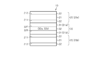
- the figure which shows the cross-section of the light control sheet provided with the transparent resin base material which has 1st layer structure.
- a light control sheet and an embodiment embodying the light control device will be described with reference to FIGS. 1 to 4. Below, the structure of the light control apparatus, the layer structure of the light control sheet, the structure of the light control layer, and the layer structure of the light transmitting resin base material will be described in order.
- FIG. 1 and FIG. 2 a normal type and a reverse type, which are types of light control devices, will be described.
- the thickness of the light control layer, the thickness of the light transmitting resin substrate, the size of the domain, the size of the liquid crystal molecules, and the like are exaggeratedly shown. .
- the light control device includes a light control sheet 10 and a voltage control unit 40 connected to the light control sheet 10.
- the light control sheet 10 changes the transmittance of the light control sheet 10 by switching the direction in which the liquid crystal molecules are aligned.
- the voltage control unit 40 controls the application of a drive voltage for switching the direction in which the liquid crystal molecules are aligned.
- the light control sheet 10 includes a pair of light transmitting resin substrates 20 and a light adjusting layer 30 sandwiched by the pair of light transmitting resin substrates 20.
- the light control layer 30 includes a pair of electrode layers 31 and a liquid crystal layer 32 sandwiched by the pair of electrode layers 31.
- the liquid crystal layer 32 is formed of a polymer network liquid crystal (PNLC).
- PNLC polymer network liquid crystal
- the liquid crystal layer 32 includes a polymer network 32 a and a liquid crystal composition 32 b.
- the polymer network 32a has a three-dimensional mesh having a plurality of domains 32c. Each domain 32c is a void defined by the polymer network 32a.
- the liquid crystal composition 32b fills the domain 32c of the polymer network 32a.
- the state of the liquid crystal layer 32 changes between a first state for scattering light and a second state for transmitting light.
- the liquid crystal layer 32 scatters the light incident from the front surface 32F and the light incident from the back surface 32R, and the scattered light is emitted from the front surface 32F and the back surface 32R.
- the liquid crystal layer 32 when no driving voltage is applied to the liquid crystal layer 32, the liquid crystal layer 32 is in the first state.
- the liquid crystal composition 32b When no driving voltage is applied to the liquid crystal layer 32, the liquid crystal composition 32b is irregularly arranged in the domain 32c. This makes it difficult for the light to pass through the liquid crystal layer 32 from the front surface 32F to the back surface 32R and from the back surface 32R to the front surface 32F. As a result, the haze value of the liquid crystal layer 32 is higher than that when the driving voltage is applied to the liquid crystal layer 32.
- the liquid crystal layer 32 when a drive voltage is applied to the liquid crystal layer 32, the liquid crystal layer 32 is in the second state.
- a driving voltage is applied to the liquid crystal layer 32, in the liquid crystal composition 32b, one direction in which the longitudinal direction of the liquid crystal composition 32b intersects the front surface 32F and the back surface 32R, for example, the normal direction of the front surface 32F and the back surface 32R Line up as you follow.
- the haze value of the liquid crystal layer 32 is smaller than when the driving voltage is not applied to the liquid crystal layer 32.
- the haze value of the liquid crystal layer 32 is relatively high, and the voltage is applied to the liquid crystal layer 32, the liquid crystal The haze value of layer 32 is relatively low.
- the possible haze value of the liquid crystal layer 32 may be only a first value corresponding to the first state and a second value corresponding to the second state.
- the liquid crystal layer 32 may be an intermediate value between the first value and the second value in the haze value depending on the magnitude of the drive voltage applied. It may be possible to take
- the total light transmittance of the liquid crystal layer 32 is preferably 10% or less, and the haze value of the liquid crystal layer 32 is preferably 80% or more.
- the total light transmittance of the liquid crystal layer 32 is preferably 80% or more, and the haze value of the liquid crystal layer 32 is preferably 10% or less.
- the total light transmittance of each layer can be measured by a method according to JIS K 7361-1 (ISO 13468-1).
- the haze value of each layer can be measured by a method in accordance with JIS K 7136 (ISO 14782).
- the pair of electrode layers 31 transmit light and apply a driving voltage to the liquid crystal layer 32.
- the electrode layer 31 is positioned on the surface 32F of the liquid crystal layer 32 and on the back surface 32R.
- the electrode layer 31 located on the surface 32F of the liquid crystal layer 32 is the first electrode layer 31a
- the electrode layer 31 located on the back surface 32R of the liquid crystal layer 32 is the second electrode layer 31b. is there.
- the total light transmittance of each electrode layer 31 is preferably higher than the total light transmittance of the liquid crystal layer 32 when the liquid crystal layer 32 is in the second state.
- the total light transmittance of the light control sheet 10 is substantially determined by the total light transmittance of the liquid crystal layer 32.
- the pair of light transmitting resin substrates 20 is configured of a first light transmitting resin substrate 20 a and a second light transmitting resin substrate 20 b.
- the first light transmitting resin base material 20a is bonded to the surface of the first electrode layer 31a opposite to the surface in contact with the surface 32F of the liquid crystal layer 32.
- the second light transmitting resin base material 20b is bonded to the surface of the second electrode layer 31b opposite to the surface in contact with the back surface 32R of the liquid crystal layer 32.
- each light transmissive resin base 20a, 20b be higher than the total light transmittance of the liquid crystal layer 32 when the liquid crystal layer 32 is in the second state.
- the total light transmittance of the light control sheet 10 is substantially determined by the total light transmittance of the liquid crystal layer 32.
- Each light transmissive resin base 20a, 20b is provided with a flexible light transmissive resin sheet.
- the light control sheet 10 also has flexibility because each light transmitting resin base material 20a and 20b has flexibility.
- Such a light control sheet 10 can be applied to a member including a curved surface shape in addition to being laminated on a flat member such as glass, and can be stored in a state in which the light control sheet 10 is wound up. is there.
- the freedom degree of handling increases.
- the light control sheet 10 is equipped with a pair of light transmissive resin base material 20 and the light control layer 30 pinched
- the light control layer 30 includes a pair of electrode layers 31, a pair of alignment layers 33 sandwiched by the pair of electrode layers 31, and a liquid crystal layer 32 sandwiched by the pair of alignment layers 33.
- one alignment layer 33 is a first alignment layer 33a located between the surface 32F of the liquid crystal layer 32 and the first electrode layer 31a.
- the other alignment layer 33 of the pair of alignment layers 33 is a second alignment layer 33 b located between the back surface 32 R of the liquid crystal layer 32 and the second electrode layer 31 b.
- the alignment layers 33a and 33b are, for example, vertical alignment films, and align the liquid crystal compositions 32b such that the extending direction of the liquid crystal molecules is along the normal direction of the plane in which the alignment layers 33a and 33b extend. Therefore, when the drive voltage is not applied to the liquid crystal layer 32, the liquid crystal layer 32 is in the second state. That is, in the domains, the liquid crystal composition 32b is aligned such that the extending direction of the liquid crystal molecules is along the normal direction of the plane in which the alignment layers 33a and 33b extend. Thus, light can easily pass through the liquid crystal layer 32 from the front surface 32F to the back surface 32R and from the back surface 32R to the front surface 32F.
- the haze value in the liquid crystal layer 32 is lower than that when the driving voltage is applied to the liquid crystal layer 32.
- the liquid crystal layer 32 is in the first state. That is, in the domain 32c, the liquid crystal composition 32b is aligned such that the extending directions of the liquid crystal molecules are irregular. This makes it difficult for the light to pass through the liquid crystal layer 32 from the front surface 32F to the back surface 32R and from the back surface 32R to the front surface 32F.
- the haze value in the liquid crystal layer 32 is higher than when the voltage is not applied to the liquid crystal layer 32.
- the haze value of the liquid crystal layer 32 is relatively high, and when the voltage is not applied to the liquid crystal layer 32, The haze value is relatively low.
- the resin forming the polymer network 32a is, for example, either a thermosetting resin or an ultraviolet curable resin.
- the resin forming the polymer network 32a is formed of, for example, a monomer having a polar group and a bifunctional monomer.
- the monomer having a polar group and the difunctional monomer are polymerized by the application of heat thereto, or by the irradiation of ultraviolet rays thereto.
- the monomer having a polar group has, for example, at least one polar group selected from the group consisting of a hydroxy group, a carboxy group, and a phosphoric acid group.
- the liquid crystal composition 32 b is, for example, any of liquid crystal molecules forming nematic liquid crystal, liquid crystal molecules forming smectic liquid crystal, and liquid crystal molecules forming cholestick liquid crystal.
- the liquid crystal composition 32b can also contain a dichroic dye, an ultraviolet light absorber, and the like as components other than liquid crystal molecules.
- the liquid crystal layer 32 can be manufactured by the following manufacturing method. First, a composition containing a liquid crystal composition 32 b and an ultraviolet polymerizable compound is sealed between a pair of light transmitting resin substrates 20 to which the electrode layer 31 is bonded. Next, ultraviolet rays are applied to the enclosed composition, for example, from the side opposite to the composition with respect to the first electrode layer 31a and from the side opposite to the composition with respect to the second electrode layer 31b. As a result, the ultraviolet polymerizable compound is photopolymerized to form a polymer, and the polymer is crosslinked to form a large number of fine domains 32c. As a result, a polymer network 32a is formed.
- polymerization speed in a ultraviolet polymeric compound can be suppressed in the thickness direction of the polymer network 32a.
- the electrode layer 31 is a conductive film having light transparency.
- the material constituting the electrode layer 31 is, for example, a light-transmitting conductive polymer.
- the conductive polymers are, for example, polythiophenes, polyacetylenes, polyanilines and polypyrroles.
- An example of a polythiophene-based polymer is PEDOT (Polyethylenedioxythiophene).
- the material forming the electrode layer 31 is, for example, a light transmitting metal oxide having conductivity.
- the metal oxides are, for example, ATO (SnO 2 : Sb), FTO (SnO 2 : F), ITO (In 2 O 3 : Sn), AZO (ZnO: Al), and GZO (ZnO: Ga). .
- the layer structure of the light transmitting resin base 20 will be described with reference to FIGS. 3 and 4. In addition, below, as a layer structure of the transparent resin base material 20, 1st layer structure and 2nd layer structure are demonstrated.
- the transparent resin base material 20 is equipped with the transparent resin sheet 21 and the surface treatment layer 22.
- the surface treatment layer 22 is positioned on each of the first surface 211 and the second surface 212 of the light transmitting resin sheet 21.
- the surface treatment layer 22 may be located on only one of the first surface 211 and the second surface 212.
- the light transmitting resin sheet 21 has light transmitting property and flexibility.
- the material constituting the light transmitting resin sheet 21 is made of, for example, PET, polyethylene (PE), polycarbonate (PC), polyethylene naphthalate (PEN), and polyimide (PI) It is any one selected from the group.
- the glass transition temperature of the light transmitting resin sheet 21 is preferably 85 ° C. or higher from the viewpoint of enhancing the resistance in a high temperature and humid environment.
- the material forming the light transmitting resin sheet 21 is preferably polycarbonate, polyethylene naphthalate, and polyimide.
- the glass transition temperature of polyethylene is about -125 ° C, and the glass transition temperature of polyethylene terephthalate is about 69 ° C.
- the glass transition temperature of polyethylene naphthalate is about 80 ° C.
- the glass transition temperature of polycarbonate is about 150 ° C.
- the glass transition temperature of polyimide is about 275 ° C.
- the high temperature and high humidity environment is an environment having a temperature of 85 ° C. and a relative humidity (RH) of 85%.
- the thickness of the light transmitting resin sheet 21 is, for example, 50 ⁇ m or more and 200 ⁇ m or less.
- the thickness of the light transmitting resin sheet 21 is 50 ⁇ m or more, it is possible to suppress the generation of wrinkles and the like in the light transmitting resin sheet 21 when manufacturing the light control sheet 10.
- the thickness of the light transmitting resin sheet 21 is 200 ⁇ m or less, it is easy to ensure the light transmitting property of the light control sheet 10.
- the content of low molecular impurities such as oligomers is preferably low. As the content of the low molecular weight impurity is lower, the low molecular weight impurity is less likely to be generated in the light transmitting resin sheet 21 in a high temperature and humid environment, and the low molecular weight impurity is less likely to move to the light control layer 30.
- the surface treatment layer 22 is at least one of a hard coat layer and a diffusion suppression layer.
- the number of layers constituting a single surface treatment layer 22 is one or more.
- the single surface treatment layer 22 may be composed of only a hard coat layer, or may be composed only of a diffusion suppression layer.
- the single surface treatment layer 22 may be composed of, for example, a hard coat layer and an adhesive layer, or may be composed of a diffusion suppression layer and an adhesive layer.
- the single surface treatment layer 22 may be a combination of a hard coat layer and a diffusion suppression layer.
- the light transmitting resin base 20 may have different types of hard coat layers on the first surface 211 and the second surface 212, and the first surface 211 and the second surface 212 are different from each other.
- the light transmitting resin base material 20 may include a diffusion suppression layer on the first surface 211 and a hard coat layer on the second surface 212.
- the light transmitting resin base 20 may have a hard coat layer on the first surface 211 and a diffusion suppression layer on the second surface 212.
- the hard coat layer has a hardness higher than that of the light transmitting resin sheet 21 in a pencil hardness test in accordance with JIS K5600-5-4 (1999).
- the hard coat layer has a barrier property to suppress the diffusion of water molecules to the light control layer 30 and the diffusion of the air to the light control layer 30.
- the hard coat layer also has barrier properties to suppress the diffusion of water molecules to the light transmitting resin sheet 21 and the diffusion of the air to the light transmitting resin sheet 21.
- the hard coat layer preferably has a glass transition temperature (Tg) higher than that of the light transmitting resin sheet 21.
- the hard coat layer is, for example, at least one selected from the group consisting of a cured product of a photocurable resin, a cured product of a thermosetting resin, and an inorganic oxide film.
- the hardcoat layer is formed by a method of supplying energy to the curable resin located in the light transmitting resin sheet. It is possible to form.
- the number of layers constituting a single hard coat layer is one or more.
- the single hard coat layer may be made of, for example, only a cured product of a photocurable resin, or a combination of a cured product of a photocurable resin and an inorganic oxide film.
- the single hard coat layer may be a combination of a cured product of a photocurable resin or a cured product of a thermosetting resin and an inorganic oxide film.
- the photocurable resin for forming the hard coat layer is, for example, an acrylate resin, an acrylic resin, a polyester resin, and an epoxy resin.
- the monomers or prepolymers that form the acrylate resin are, for example, polyester acrylates and epoxy acrylates.
- the thermosetting resin that constitutes the hard coat layer is, for example, a polycarbonate resin and a polyimide resin.
- the monomer or prepolymer forming the hard coat layer preferably has two or more unsaturated double bonds from the viewpoint of obtaining high barrier properties.
- the thickness of the hard coat layer is, for example, 0.2 ⁇ m or more and 10 ⁇ m or less.
- the thickness of the hard coat layer is 0.1 ⁇ m or more, it becomes possible to obtain sufficient barrier properties by suppressing formation of pinholes and the like in the hard coat layer.
- the thickness of the hard coat layer is 10 ⁇ m or less, it is possible to suppress the decrease in transmittance due to the addition of the hard coat layer separately.
- the diffusion of low molecular impurities from the light transmitting resin sheet 21 to the light control layer 30 can be suppressed in a high temperature and humid environment.
- the hard coat layer is provided on the second surface 212, it is possible to suppress hydrolysis in the light transmitting resin sheet 21 in a high temperature and high humidity environment, thereby generating low molecular impurities by hydrolysis. It is possible to suppress itself.
- the hard coat layer may be in contact with the electrode layer 31 or may be bonded to the electrode layer 31 via an easy adhesion layer.
- the resin forming the easy adhesion layer includes, for example, at least one or more polymers selected from the group consisting of acrylic polymers, polyesters, polyurethanes, polyvinyl alcohols, polyester acrylates, urethane acrylates, and epoxy acrylates.
- the diffusion suppression layer includes a polymer network for suppressing the diffusion of the low molecular weight impurity, and thereby has a barrier property to suppress the diffusion of the low molecular weight impurity.
- low molecular impurities such as oligomers are unavoidably contained in the light transmitting resin sheet 21 when the light transmitting resin sheet 21 is produced.
- low molecular impurities are generated in the light transmitting resin sheet 21 by placing the light transmitting resin sheet 21 in a high temperature and high humidity environment.
- the diffusion suppression layer is, for example, at least one selected from the group consisting of a cured product of a photocurable resin, a cured product of a thermosetting resin, and an inorganic oxide film.
- the number of layers constituting a single diffusion suppression layer is one or more.
- the single diffusion suppressing layer may be composed of only the cured product of the photocurable resin, or may be a combination of the cured product of the photocurable resin and the inorganic oxide film.
- the single diffusion suppressing layer may be a combination of a cured product of a photocurable resin or a cured product of a thermosetting resin and an inorganic oxide film.
- the material which comprises a diffusion suppression layer is a crosslinked body of the composition which has a functional group which forms a crosslinked structure.
- the composition contains, for example, one or more polymers selected from the group consisting of acrylic polymers, polyesters, polyurethanes, polyvinyl alcohols, polyester acrylates, polyurethane acrylates, and polyepoxy acrylates. Therefore, the diffusion suppressing layer can easily suppress the diffusion of low molecular impurities into the light control layer 30. Furthermore, since it becomes possible to provide the diffusion suppression layer with the function of bonding the light control layer 30 and the light transmitting resin sheet 21, the adhesion between the light control layer 30 and the light transmitting resin sheet 21 is enhanced. Is also possible.
- the light control sheet 10 may include an easy adhesion layer for bonding the light transmitting resin sheet 21 and the light control layer 30.
- the material forming the diffusion suppression layer may be, for example, the same as the material forming the easy adhesion layer.
- the thickness of the easy adhesion layer is usually 10 nm or more and 100 nm or less.
- the total of the thickness of the easy adhesion layer and the thickness of the diffusion suppression layer is, for example, 1 ⁇ m or more and 10 ⁇ m or less.
- the present inventors have used a polyethylene terephthalate sheet as the light transmitting resin sheet 21 and have a conventional structure in which the light transmitting resin sheet 21 and the light control layer 30 are joined by the easy adhesion layer in a high temperature and humidity environment.
- the state of the light control sheet 10 was earnestly studied. Among them, it was found that low molecular impurities such as oligomers are diffused from the light transmitting resin sheet 21 in a high temperature and humid environment and deposited in the liquid crystal layer 32, thereby disturbing the alignment of liquid crystal molecules. .
- each light transmitting resin base 20 is formed of a single light transmitting resin sheet 21.
- the light transmitting resin sheet 21 in the second layer structure has light transmitting property and flexibility.
- the material which comprises the transparent resin sheet 21 is any one compound selected from the group consisting of polyethylene naphthalate and polyimide. That is, the light transmitting resin sheet 21 is a polyethylene naphthalate sheet or a polyimide sheet. Polyethylene naphthalate sheets and polyimide sheets are superior in resistance to hydrolysis as compared to PET sheets. Therefore, it is easy to reduce the low molecular impurities moving from the light transmitting resin sheet 21.
- the light transmitting resin sheet 21 may be in contact with the electrode layer 31 or may be bonded to the electrode layer 31 via the easy adhesion layer.
- the electrode structure which is a structure in which the light transmitting resin sheet 21 and the electrode layer 31 are joined satisfies the following [Condition 1]. Moreover, it is preferable that an electrode structure satisfy
- the present inventors relate the relationship between the movement of low molecular impurities and the increase in the haze value of the electrode structure. I found it. That is, when the increase in the haze value in the electrode structure is as high as 3%, a defect in the alignment control due to the movement of low molecular impurities is recognized, while if the increase in the haze value is less than 2%, It has been found that the reliability of orientation control by the movement of low molecular impurities can be secured. Then, as described above, if the light control sheet 10 satisfies the condition 1 !, it is possible to suppress the diffusion and generation of low molecular impurities.
- Example 1 The normal type light control sheet 10 of Example 1 provided with the following layers was obtained. Further, a pair of alignment layers 33 were added to the light control sheet 10 of Example 1, to obtain a reverse type light control sheet 10 of Example 2.
- -Layer structure of light transmitting resin substrate 20 First layer structure-Light transmitting resin sheet 21: PET sheet (A4300 manufactured by Toyobo Co., Ltd.) ⁇ Thickness of light transmitting resin sheet 21: 50 ⁇ m ⁇
- Surface treatment layer 22 hard coat layer (acrylic resin) ⁇ Thickness of surface treatment layer 22: 1.0 ⁇ m .
- Examples 3 and 4 The thickness of the surface treatment layer 22 of Example 1 was changed to 1.5 ⁇ m, and the other components were the same as in Example 1, and a light control sheet 10 of Example 3 was obtained. Further, as in Example 2, a pair of alignment layers 33 was added to the light control sheet 10 of Example 3, to obtain a reverse light control sheet 10 of Example 4.
- Examples 5, 6 The thickness of the surface treatment layer 22 of Example 1 was changed to 3.0 ⁇ m, and the other components were the same as in Example 1, to obtain a light control sheet 10 of Example 5. Further, as in Example 2, by adding a pair of alignment layers 33 to the light control sheet 10 of Example 5, a reverse-type light control sheet 10 of Example 6 was obtained.
- Example 7 The thickness of the surface treatment layer 22 of Example 1 was changed to 5.0 ⁇ m, and the other components were the same as in Example 1, to obtain a light control sheet 10 of Example 7. Further, in the same manner as in Example 2, by adding a pair of alignment layers 33 to the light control sheet 10 in Example 7, a reverse-type light control sheet 10 in Example 8 was obtained.
- Examples 9, 10 The electrode layer 31 of Example 1 is changed to ITO having a thickness of 0.02 ⁇ m, and the thickness of the surface treatment layer 22 is changed to 1.5 ⁇ m, and the other components are the same as in Example 1.
- the light control sheet 10 of Example 9 was obtained. Further, in the same manner as in Example 2, by adding a pair of alignment layers 33 to the light control sheet 10 in Example 7, a reverse-type light control sheet 10 in Example 10 was obtained.
- Example 11 The light control sheet 10 of Example 11 is the same as Example 1 except that the surface treatment layer 22 of Example 1 is changed to a diffusion suppression layer (acrylic resin) having a thickness of 1.0 ⁇ m. I got Further, as in the case of Example 2, as a configuration in which a pair of alignment layers 33 were added to the light control sheet 10 of Example 11, a reverse-type light control sheet 10 of Example 8 was obtained.
- a diffusion suppression layer acrylic resin
- Example 13 The light control sheet 10 of Example 13 provided with the following layers was obtained. Further, in the same manner as in Example 2, by adding a pair of alignment layers 33 to the light control sheet 10 in Example 13, a reverse type light control sheet 10 in Example 14 was obtained.
- -Layer structure of light transmitting resin base 20 Second layer structure-Light transmitting resin sheet 21: PEN sheet (manufactured by Teijin Limited) ⁇ Thickness of light transmitting resin sheet 21: 50 ⁇ m ⁇
- Example 15 The light control sheet 10 of Example 15 provided with the following layers was obtained. Further, as in Example 2, a pair of alignment layers 33 was added to the light control sheet 10 of Example 15, to obtain a reverse light control sheet 10 of Example 16.
- -Layer structure of light transmitting resin base 20 Second layer structure-Light transmitting resin sheet 21: PI sheet (manufactured by Kaneka Corporation) ⁇ Thickness of light transmitting resin sheet 21: 50 ⁇ m ⁇
- Example 17 The light control sheet 10 of Example 17 which has the following layer was obtained. Further, as in Example 2, a pair of alignment layers 33 was added to the light control sheet 10 of Example 17, to obtain a reverse light control sheet 10 of Example 18.
- -Layer structure of light transmitting resin substrate 20 Second layer structure-Light transmitting resin sheet 21: PET sheet (A4300 manufactured by Toyobo Co., Ltd.) ⁇ Thickness of light transmitting resin sheet 21: 50 ⁇ m ⁇
- Comparative Examples 1 and 2 The surface treatment layer 22 was omitted from the light control sheet 10 of Example 1, and the other components were the same as those of Example 1. Thus, a light control sheet of Comparative Example 1 was obtained. Further, as in Example 2, by adding a pair of alignment layers 33 to the light control sheet of Comparative Example 1, a reverse-type light control sheet 10 of Comparative Example 2 was obtained.
- Examples 1 to 18 and Comparative Examples 1 and 2 the single unit before and after the treatment at 85 ° C. and 85% RH for 100 hours using the method according to JIS K 7136 (ISO 14782) The haze value of the light transmitting resin substrate 20 was measured.
- Examples 1 to 18 and Comparative Examples 1 and 2 the haze value before treatment and the difference between the haze value before treatment and the haze value after treatment for the light transmitting resin substrate 20 as a single body The rise amount of the haze value is shown in Tables 1 and 2.
- the haze value of the structure was measured. Further, using the method according to JIS K 5600-5-1 (flexibility (cylindrical mandrel)), the flex resistance test was performed on the electrode structure.
- the haze value of the electrode structure before the treatment and the increase in the haze value which is the difference between the haze values before and after the treatment are shown in Tables 1 and 2. Show.
- the minimum diameter of the mandrel in which no crack was generated in the electrode structure is shown as flexibility in Tables 1 and 2.
- the voltage applied to the light control sheet is from 0 V to 10 V It changed and the minimum value of the haze value in a light control sheet was measured.
- the minimum value of the haze value is a value measured using a method according to JIS K 7136 (ISO 14782), and the haze value when the state of the light control layer is changed from the first state to the second state It is the minimum value.
- the maximum value of the transmittance of the light control sheet between the first state and the second state was measured using a method in accordance with JIS K 7361-1 (ISO 13468-1).
- the minimum value of the haze value of the light control sheet in the normal type and the maximum value of the transmittance in Examples 1 to 18 and Comparative Examples 1 and 2 are shown in Tables 1 and 2.
- Example 1 to 18 and Comparative Examples 1 and 2 after the reverse-type light control sheet is treated at 85 ° C. and 85% RH for 100 hours, the voltage applied to the light control sheet is from 0 V to 10 V It changed and measured the maximum value of the haze value in a light control sheet.
- the maximum value of the haze value is a value measured using a method according to JIS K 7136 (ISO 14782), and the haze value when the state of the light control layer is changed from the first state to the second state It is the maximum value.
- the minimum value of the transmittance of the light control sheet was measured between the first state and the second state using a method in accordance with JIS K 7361-1 (ISO 13468-1).
- the maximum value of the haze value of the light control sheet in the reverse type and the minimum value of the transmittance in Examples 1 to 18 and Comparative Examples 1 and 2 are shown in Tables 1 and 2.
- a level satisfying all the following conditions is indicated by an “o” mark, and a level not satisfying any of the conditions is indicated by an “x” mark.
- the increase in the haze value of the light transmitting resin sheet is less than 2%.
- Normal type The minimum value of the haze value is 10% or less.
- Normal type The maximum value of transmittance is 80% or more.
- Reverse type The maximum value of the haze value is 80% or more.
- Reverse type The minimum value of transmittance is 10% or less.
- the increase in the haze value is 0.0% or more and 1.9% or less, and all levels satisfy the condition 1 Admitted.
- the increase in haze value was 3.0%, and it was found that Condition 1 was not satisfied at any level.
- the increase in the haze value was 0.2% or more and 1.9% or less, and it was found that Condition 2 satisfied all levels.
- the minimum value of the haze value is 7% or more and 9% or less, and 10% or less which has sufficient resistance in a high temperature and humid environment. It was recognized that there was.
- the maximum value of the haze value is 82% or more and 88% or less, and 80% or more which has sufficient resistance in a high temperature and humid environment. It was recognized that there was.
- the maximum value of the transmittance is 82% or more and 87% or less, and 80% or more which has sufficient resistance in a high temperature and humid environment. It was recognized that there was.
- the minimum value of the transmittance is 7% to 9%, and 10% or less which has sufficient resistance in a high temperature and humid environment. It was recognized that there was.
- the minimum value of the haze value is 12%
- the maximum value of the transmittance is 87%
- the light control sheet of Comparative Example 1 has the viewpoint of the haze value. It has been found that it does not have sufficient resistance in a hot and humid environment.
- the maximum value of the haze value is 78%
- the minimum value of the transmittance is 15%.
- the light control sheet of Comparative Example 2 in both the haze value and the transmittance Were found to be not well tolerated in hot and humid environments.
- the diffusion suppression layer is provided as the surface treatment layer 22 (Examples 11 to 12) or if [Condition 1] is satisfied (Examples 1 to 18), the alignment control using liquid crystal molecules is also performed similarly. It becomes possible to secure sufficient reliability. Furthermore, when [Condition 2] is satisfied (Examples 13 to 18), in the state where the surface treatment layer 22 is omitted, it is possible to sufficiently ensure the reliability of alignment control using liquid crystal molecules as well. .
- the following effects can be obtained. (1) When the surface treatment layer 22 is provided, diffusion of low molecular impurities and generation of low molecular impurities in the light transmitting resin sheet 21 can be suppressed. Therefore, it becomes possible to improve the reliability of orientation control in a high temperature and high humidity environment. (2) When the surface treatment layer 22 is located on the first surface 211, it is possible to suppress the low molecular impurities from reaching the light control layer 30 immediately before the light control layer 30.
- the surface treatment layer 22 is a cured product of a photocurable resin or a cured product of a thermosetting resin, energy for curing the curable resin is supplied through the light transmitting resin sheet 21 Is also possible.
- the adhesion between the light transmitting resin sheet 21 and the light control layer 30 can be enhanced. It will be.
- the electrode layer 31 made of a conductive polymer usually has excellent flexibility while transmitting low molecular impurities more easily than conductive metal oxides. Therefore, when the electrode layer 31 is made of a conductive polymer, it is possible to improve the reliability of orientation control in a high temperature and humidity environment and provide the light control sheet 10 excellent in flexibility. It will be.
- Liquid crystal layer 32 The type of the liquid crystal layer 32 can be changed to polymer dispersed liquid crystal (PDLC) or capsule-type nematic liquid crystal (NCAP).
- the polymer dispersed liquid crystal has a large number of isolated voids in the polymer layer, and holds the liquid crystal composition in the voids dispersed in the polymer layer.
- the capsule nematic liquid crystal holds the liquid crystal composition having a capsule shape in the polymer layer.
- One light transmitting resin substrate 20 included in the light control sheet has a structure according to the first layer structure described above, and the other light transmitting resin substrate has a structure according to the second layer structure described above It is also possible. That is, one light transmitting resin base material 20 may be provided with the surface treatment layer 22, and the other light transmitting resin base material 20 may be constituted only by the light transmitting resin sheet 21 satisfying the condition 2.
Abstract
A light control sheet (10) according to the present invention is provided with: a light-transmitting resin base material (20); and a light control layer (30) which is supported by the light-transmitting resin base material (20). The light control layer (30) is provided with: a liquid crystal layer (32); and a pair of electrode layers (31) that sandwich the liquid crystal layer (32). The light-transmitting resin base material (20) is provided with: a light-transmitting resin sheet (21) which has a first surface (211) that faces the light control layer (30) and a second surface (212) that is on the reverse side of the first surface (211); and a surface treatment layer (22) which is arranged on at least one of the first surface (211) and the second surface (212), and which has barrier properties.
Description
本発明は、調光シート、および、調光シートを備えた調光装置に関する。
The present invention relates to a light control sheet and a light control device provided with the light control sheet.
調光シートは、一対の光透過性樹脂シートと液晶層とを備える。液晶層は、一対の光透過性樹脂シートの間に位置する。調光シートにおいて、液晶層に印加する電圧の変更によって液晶分子の配向する方向が変わる。調光シートの型式には、配向膜を有しないノーマル型と、配向膜を有するリバース型とが存在する。ノーマル型は、駆動電圧の印加によって液晶層の透過率を上げ、駆動電圧の印加の停止によって液晶層の透過率を下げる。リバース型は、駆動電圧の印加によって液晶層の透過率を下げ、駆動電圧の印加の停止によって液晶層の透過率を上げる(例えば、特許文献1参照)。
The light control sheet includes a pair of light transmitting resin sheets and a liquid crystal layer. The liquid crystal layer is located between the pair of light transmitting resin sheets. In the light control sheet, the orientation direction of the liquid crystal molecules is changed by changing the voltage applied to the liquid crystal layer. There are two types of light control sheets, a normal type having no alignment film and a reverse type having an alignment film. In the normal type, the transmittance of the liquid crystal layer is increased by the application of the drive voltage, and the transmittance of the liquid crystal layer is reduced by the stop of the application of the drive voltage. In the reverse type, the transmittance of the liquid crystal layer is lowered by application of a driving voltage, and the transmittance of the liquid crystal layer is increased by stopping the application of the driving voltage (see, for example, Patent Document 1).
調光シートが適用される対象は、パーティションなどの内装建材や、映像を映し出すスクリーンなどである。調光シートが置かれる環境は、温度や湿度の調整された室内環境である。室内環境での使用を前提とした調光シートが備える光透過性樹脂シートは、例えば、ポリエチレンテレフタラートシート(polyethylene terephthalateシート:PETシート)であり、室内環境では安定した化学的な性質を有する。
The objects to which the light control sheet is applied are interior construction materials such as partitions, and screens for projecting images. The environment where the light control sheet is placed is an indoor environment in which the temperature and humidity are adjusted. The light transmitting resin sheet included in the light control sheet intended for use in the indoor environment is, for example, a polyethylene terephthalate sheet (polyethylene terephthalate sheet: PET sheet), and has stable chemical properties in the indoor environment.
近年、調光シートが適用される対象は、航空機の窓、自動車の投光装置、自動車の窓などにまで広がり、調光シートが置かれる環境もまた、温度や湿度が大きく変わる空間にまで広がっている。そして、新たな環境に対して耐性を高めるための要請は、調光シートにおいて高まる一途である。特に、高温かつ多湿の環境においては、新たな課題として、液晶分子の配向する方向が電圧の印加に追従しにくい現象が発生している。
本発明の目的は、高温かつ多湿の環境における配向制御の信頼性を向上可能とした調光シート、および、調光シートを備える調光装置を提供することである。 In recent years, the target to which the light control sheet is applied extends to the window of an aircraft, a light projector of an automobile, the window of a car, etc. The environment where the light control sheet is placed also extends to a space where temperature and humidity change greatly. ing. And the demand for enhancing resistance to new environments is ever increasing in light control sheets. In particular, in a high temperature and high humidity environment, as a new problem, a phenomenon occurs in which the direction in which the liquid crystal molecules are aligned does not easily follow the application of a voltage.
An object of the present invention is to provide a light control sheet capable of improving the reliability of orientation control in a high temperature and humidity environment, and a light control device including the light control sheet.
上記課題を解決するための調光シートは、光透過性樹脂基材と、前記光透過性樹脂基材に支持される調光層と、を備える。前記調光層は、液晶層と、前記液晶層を挟む一対の電極層と、を備える。前記光透過性樹脂基材は、前記調光層と対向する第1面と、前記第1面とは反対側の面である第2面とを備える光透過性樹脂シートと、前記第1面および前記第2面の少なくとも一方に位置し、バリア性を有した表面処理層と、を備える。
The light control sheet for solving the said subject is provided with a light transmissive resin base material and the light control layer supported by the said light transmissive resin base material. The light control layer includes a liquid crystal layer and a pair of electrode layers sandwiching the liquid crystal layer. A light transmitting resin sheet comprising: a first surface facing the light control layer; and a second surface opposite to the first surface, and the first surface And a surface treatment layer located on at least one of the second surfaces and having a barrier property.
上記課題を解決するための調光シートは、光透過性樹脂基材と、前記光透過性樹脂基材に支持される調光層と、を備える。前記調光層は、液晶層と、前記液晶層を挟む電極層と、を備える。前記電極層と、前記電極層と接合した前記光透過性樹脂基材とからなる構造体において、温度が85℃かつ相対湿度が85%の条件下で100時間処理後のヘイズ値の上昇率が2%未満である。
The light control sheet for solving the said subject is provided with a light transmissive resin base material and the light control layer supported by the said light transmissive resin base material. The light control layer includes a liquid crystal layer and an electrode layer sandwiching the liquid crystal layer. In the structure composed of the electrode layer and the light transmitting resin base joined to the electrode layer, the increase rate of the haze value after 100 hours of treatment under the condition of a temperature of 85 ° C. and a relative humidity of 85% It is less than 2%.
上記課題を解決するための調光装置は、上記調光シートと、前記調光シートが備える電極層に対する駆動電圧の印加を制御する電圧制御部と、を備える。
The light control apparatus for solving the said subject is provided with the said light control sheet | seat, and the voltage control part which controls the application of the drive voltage with respect to the electrode layer with which the said light control sheet is equipped.
図1から図4を参照して、調光シート、および、調光装置を具体化した一実施形態を説明する。以下では、調光装置の構造、調光シートの層構造、調光層の構造、および、光透過性樹脂基材の層構造を順に説明する。
A light control sheet and an embodiment embodying the light control device will be described with reference to FIGS. 1 to 4. Below, the structure of the light control apparatus, the layer structure of the light control sheet, the structure of the light control layer, and the layer structure of the light transmitting resin base material will be described in order.
[調光装置の構造]
図1、および、図2を参照し、調光装置の型式であるノーマル型、および、リバース型を説明する。なお、図1、および、図2では、図示の便宜上、調光層の厚さ、光透過性樹脂基材の厚さ、ドメインの大きさ、および、液晶分子の大きさなどを誇張して示す。 [Structure of light control device]
With reference to FIG. 1 and FIG. 2, a normal type and a reverse type, which are types of light control devices, will be described. In FIGS. 1 and 2, for convenience of illustration, the thickness of the light control layer, the thickness of the light transmitting resin substrate, the size of the domain, the size of the liquid crystal molecules, and the like are exaggeratedly shown. .
図1が示すように、調光装置は、調光シート10と、調光シート10に接続された電圧制御部40とを備える。調光シート10は、液晶分子の配向する方向を切り替えることによって、調光シート10の透過率を変える。電圧制御部40は、液晶分子の配向する方向を切り替えるための駆動電圧の印加を制御する。
As shown in FIG. 1, the light control device includes a light control sheet 10 and a voltage control unit 40 connected to the light control sheet 10. The light control sheet 10 changes the transmittance of the light control sheet 10 by switching the direction in which the liquid crystal molecules are aligned. The voltage control unit 40 controls the application of a drive voltage for switching the direction in which the liquid crystal molecules are aligned.
[調光シートの構造:ノーマル型]
調光シート10は、一対の光透過性樹脂基材20と、一対の光透過性樹脂基材20によって挟まれた調光層30とを備える。調光層30は、一対の電極層31と、一対の電極層31によって挟まれた液晶層32とを備える。液晶層32は、ポリマーネットワーク型液晶(Polymer Network Liquid Crystal:PNLC)によって形成される。液晶層32は、ポリマーネットワーク32aと、液晶組成物32bとを含む。 [Structure of light control sheet: normal type]
Thelight control sheet 10 includes a pair of light transmitting resin substrates 20 and a light adjusting layer 30 sandwiched by the pair of light transmitting resin substrates 20. The light control layer 30 includes a pair of electrode layers 31 and a liquid crystal layer 32 sandwiched by the pair of electrode layers 31. The liquid crystal layer 32 is formed of a polymer network liquid crystal (PNLC). The liquid crystal layer 32 includes a polymer network 32 a and a liquid crystal composition 32 b.
調光シート10は、一対の光透過性樹脂基材20と、一対の光透過性樹脂基材20によって挟まれた調光層30とを備える。調光層30は、一対の電極層31と、一対の電極層31によって挟まれた液晶層32とを備える。液晶層32は、ポリマーネットワーク型液晶(Polymer Network Liquid Crystal:PNLC)によって形成される。液晶層32は、ポリマーネットワーク32aと、液晶組成物32bとを含む。 [Structure of light control sheet: normal type]
The
ポリマーネットワーク32aは、複数のドメイン32cを有した三次元の網目状を有する。各ドメイン32cは、ポリマーネットワーク32aによって区画される空隙である。液晶組成物32bは、ポリマーネットワーク32aのドメイン32cを埋めている。
The polymer network 32a has a three-dimensional mesh having a plurality of domains 32c. Each domain 32c is a void defined by the polymer network 32a. The liquid crystal composition 32b fills the domain 32c of the polymer network 32a.
液晶層32に印加される電圧の大きさが変わると、液晶層32の状態は、光を散乱する第1状態と、光を透過する第2状態との間で変わる。第1状態では、液晶層32は、表面32Fから入射した光、および、裏面32Rから入射した光を散乱し、散乱光が表面32Fおよび裏面32Rから射出される。
When the magnitude of the voltage applied to the liquid crystal layer 32 changes, the state of the liquid crystal layer 32 changes between a first state for scattering light and a second state for transmitting light. In the first state, the liquid crystal layer 32 scatters the light incident from the front surface 32F and the light incident from the back surface 32R, and the scattered light is emitted from the front surface 32F and the back surface 32R.
例えば、液晶層32に駆動電圧が印加されていないとき、液晶層32の状態は第1状態である。液晶層32に駆動電圧が印加されていないとき、液晶組成物32bは、ドメイン32c内において不規則に並んでいる。これによって、表面32Fから裏面32Rに向けて、および、裏面32Rから表面32Fに向けて、液晶層32のなかを光が通りにくくなる。結果として、液晶層32に駆動電圧が印加されたときと比べて、液晶層32でのヘイズ値が高くなる。
For example, when no driving voltage is applied to the liquid crystal layer 32, the liquid crystal layer 32 is in the first state. When no driving voltage is applied to the liquid crystal layer 32, the liquid crystal composition 32b is irregularly arranged in the domain 32c. This makes it difficult for the light to pass through the liquid crystal layer 32 from the front surface 32F to the back surface 32R and from the back surface 32R to the front surface 32F. As a result, the haze value of the liquid crystal layer 32 is higher than that when the driving voltage is applied to the liquid crystal layer 32.
これに対して、液晶層32に駆動電圧が印加されているとき、液晶層32は第2状態にある。液晶層32に駆動電圧が印加されているとき、液晶組成物32bは、液晶組成物32bの長手方向が、表面32Fおよび裏面32Rと交差する1つの方向、例えば表面32Fおよび裏面32Rの法線方向に沿うように、並ぶ。これによって、表面32Fから裏面32Rに向けて、および、裏面32Rから表面32Fに向けて、液晶層32のなかを光が通りやすくなる。結果として、液晶層32に駆動電圧が印加されないときと比べて、液晶層32でのヘイズ値が小さくなる。
On the other hand, when a drive voltage is applied to the liquid crystal layer 32, the liquid crystal layer 32 is in the second state. When a driving voltage is applied to the liquid crystal layer 32, in the liquid crystal composition 32b, one direction in which the longitudinal direction of the liquid crystal composition 32b intersects the front surface 32F and the back surface 32R, for example, the normal direction of the front surface 32F and the back surface 32R Line up as you follow. Thus, light can easily pass through the liquid crystal layer 32 from the front surface 32F to the back surface 32R and from the back surface 32R to the front surface 32F. As a result, the haze value of the liquid crystal layer 32 is smaller than when the driving voltage is not applied to the liquid crystal layer 32.
このように、ノーマル型では、液晶層32に駆動電圧が印加されていないときに、液晶層32のヘイズ値が相対的に高く、かつ、液晶層32に電圧が印加されているときに、液晶層32のヘイズ値が相対的に低い。
As described above, in the normal type, when the drive voltage is not applied to the liquid crystal layer 32, the haze value of the liquid crystal layer 32 is relatively high, and the voltage is applied to the liquid crystal layer 32, the liquid crystal The haze value of layer 32 is relatively low.
なお、液晶層32が取り得るヘイズ値は、第1状態に対応する第1の値と、第2状態に対応する第2の値とのみであってもよい。あるいは、液晶層32は、第1の値および第2の値に加えて、印加される駆動電圧の大きさに応じて、ヘイズ値における第1の値と第2の値との間の中間値を取り得ることが可能でもよい。
The possible haze value of the liquid crystal layer 32 may be only a first value corresponding to the first state and a second value corresponding to the second state. Alternatively, in addition to the first value and the second value, the liquid crystal layer 32 may be an intermediate value between the first value and the second value in the haze value depending on the magnitude of the drive voltage applied. It may be possible to take
液晶層32が第1状態であるとき、液晶層32の全光線透過率は、10%以下であり、液晶層32のヘイズ値は、80%以上であることが好ましい。液晶層32が第2状態であるとき、液晶層32の全光線透過率は、80%以上であり、液晶層32のヘイズ値は、10%以下であることが好ましい。なお、各層の全光線透過率は、JIS K 7361-1(ISO 13468-1)に準拠する方法によって測定することができる。また、各層のヘイズ値は、JIS K 7136(ISO 14782)に準拠する方法によって測定することができる。
When the liquid crystal layer 32 is in the first state, the total light transmittance of the liquid crystal layer 32 is preferably 10% or less, and the haze value of the liquid crystal layer 32 is preferably 80% or more. When the liquid crystal layer 32 is in the second state, the total light transmittance of the liquid crystal layer 32 is preferably 80% or more, and the haze value of the liquid crystal layer 32 is preferably 10% or less. The total light transmittance of each layer can be measured by a method according to JIS K 7361-1 (ISO 13468-1). In addition, the haze value of each layer can be measured by a method in accordance with JIS K 7136 (ISO 14782).
一対の電極層31は、光を透過すると共に、液晶層32に駆動電圧を印加する。電極層31は、液晶層32の表面32Fと、裏面32Rとに1層ずつ位置している。一対の電極層31のうち、液晶層32の表面32Fに位置する電極層31が、第1電極層31aであり、液晶層32の裏面32Rに位置する電極層31が、第2電極層31bである。
The pair of electrode layers 31 transmit light and apply a driving voltage to the liquid crystal layer 32. The electrode layer 31 is positioned on the surface 32F of the liquid crystal layer 32 and on the back surface 32R. Of the pair of electrode layers 31, the electrode layer 31 located on the surface 32F of the liquid crystal layer 32 is the first electrode layer 31a, and the electrode layer 31 located on the back surface 32R of the liquid crystal layer 32 is the second electrode layer 31b. is there.
各電極層31の全光線透過率は、液晶層32が第2状態であるときの液晶層32の全光線透過率よりも高いことが好ましい。これによって、調光シート10の全光線透過率が、液晶層32の全光線透過率によってほぼ定められる。
The total light transmittance of each electrode layer 31 is preferably higher than the total light transmittance of the liquid crystal layer 32 when the liquid crystal layer 32 is in the second state. Thus, the total light transmittance of the light control sheet 10 is substantially determined by the total light transmittance of the liquid crystal layer 32.
一対の光透過性樹脂基材20は、第1光透過性樹脂基材20a、および、第2光透過性樹脂基材20bから構成される。第1光透過性樹脂基材20aは、第1電極層31aのうち、液晶層32の表面32Fに接する面とは反対側の面に接合されている。第2光透過性樹脂基材20bは、第2電極層31bのうち、液晶層32の裏面32Rに接する面とは反対側の面に接合されている。
The pair of light transmitting resin substrates 20 is configured of a first light transmitting resin substrate 20 a and a second light transmitting resin substrate 20 b. The first light transmitting resin base material 20a is bonded to the surface of the first electrode layer 31a opposite to the surface in contact with the surface 32F of the liquid crystal layer 32. The second light transmitting resin base material 20b is bonded to the surface of the second electrode layer 31b opposite to the surface in contact with the back surface 32R of the liquid crystal layer 32.
各光透過性樹脂基材20a,20bの全光線透過率は、液晶層32が第2状態であるときの液晶層32の全光線透過率よりも高いことが好ましい。これによって、調光シート10の全光線透過率が、液晶層32の全光線透過率よってほぼ定められる。
It is preferable that the total light transmittance of each light transmissive resin base 20a, 20b be higher than the total light transmittance of the liquid crystal layer 32 when the liquid crystal layer 32 is in the second state. Thus, the total light transmittance of the light control sheet 10 is substantially determined by the total light transmittance of the liquid crystal layer 32.
各光透過性樹脂基材20a,20bは、可撓性を有した光透過性樹脂シートを備える。各光透過性樹脂基材20a,20bが可撓性を有することによって、調光シート10も可撓性を有する。こうした調光シート10は、ガラスなどの平坦な部材に積層する以外に、曲面形状を含む部材への適用が可能であり、また、調光シート10を巻き取った状態で収納することも可能である。このように、可撓性を有する調光シート10によれば、取扱いの自由度が高まる。
Each light transmissive resin base 20a, 20b is provided with a flexible light transmissive resin sheet. The light control sheet 10 also has flexibility because each light transmitting resin base material 20a and 20b has flexibility. Such a light control sheet 10 can be applied to a member including a curved surface shape in addition to being laminated on a flat member such as glass, and can be stored in a state in which the light control sheet 10 is wound up. is there. Thus, according to the light control sheet 10 which has flexibility, the freedom degree of handling increases.
[調光シートの構造:リバース型]
図2が示すように、調光シート10は、一対の光透過性樹脂基材20と、一対の光透過性樹脂基材20によって挟まれた調光層30とを備える。調光層30は、一対の電極層31と、一対の電極層31で挟まれた一対の配向層33と、一対の配向層33によって挟まれた液晶層32とを備える。一対の配向層33のうち、一方の配向層33は、液晶層32の表面32Fと第1電極層31aとの間に位置する第1配向層33aである。一対の配向層33のうち、他方の配向層33は、液晶層32の裏面32Rと第2電極層31bとの間に位置する第2配向層33bである。 [Structure of light control sheet: reverse type]
As FIG. 2 shows, thelight control sheet 10 is equipped with a pair of light transmissive resin base material 20 and the light control layer 30 pinched | interposed by a pair of light transmissive resin base material 20. As shown in FIG. The light control layer 30 includes a pair of electrode layers 31, a pair of alignment layers 33 sandwiched by the pair of electrode layers 31, and a liquid crystal layer 32 sandwiched by the pair of alignment layers 33. Of the pair of alignment layers 33, one alignment layer 33 is a first alignment layer 33a located between the surface 32F of the liquid crystal layer 32 and the first electrode layer 31a. The other alignment layer 33 of the pair of alignment layers 33 is a second alignment layer 33 b located between the back surface 32 R of the liquid crystal layer 32 and the second electrode layer 31 b.
図2が示すように、調光シート10は、一対の光透過性樹脂基材20と、一対の光透過性樹脂基材20によって挟まれた調光層30とを備える。調光層30は、一対の電極層31と、一対の電極層31で挟まれた一対の配向層33と、一対の配向層33によって挟まれた液晶層32とを備える。一対の配向層33のうち、一方の配向層33は、液晶層32の表面32Fと第1電極層31aとの間に位置する第1配向層33aである。一対の配向層33のうち、他方の配向層33は、液晶層32の裏面32Rと第2電極層31bとの間に位置する第2配向層33bである。 [Structure of light control sheet: reverse type]
As FIG. 2 shows, the
各配向層33a,33bは、例えば、垂直配向膜であり、液晶分子の延びる方向が配向層33a,33bが広がる平面の法線方向に沿うように、各液晶組成物32bを配向する。そのため、液晶層32に駆動電圧が印加されていないとき、液晶層32は第2状態にある。すなわち、液晶組成物32bは、ドメインのなかで、液晶分子の延びる方向が、配向層33a,33bが広がる平面の法線方向に沿うように並ぶ。これによって、表面32Fから裏面32Rに向けて、および、裏面32Rから表面32Fに向けて、液晶層32のなかを光が通りやすくなる。結果として、液晶層32に駆動電圧が印加されたときと比べて、液晶層32におけるヘイズ値が低くなる。これに対して、液晶層32に駆動電圧が印加されているとき、液晶層32は第1状態にある。すなわち、液晶組成物32bは、ドメイン32cのなかで、液晶分子の延びる方向が不規則であるように並ぶ。これによって、表面32Fから裏面32Rに向けて、および、裏面32Rから表面32Fに向けて、液晶層32のなかを光が通りにくくなる。結果として、液晶層32に電圧が印加されていないときと比べて、液晶層32におけるヘイズ値が高くなる。
The alignment layers 33a and 33b are, for example, vertical alignment films, and align the liquid crystal compositions 32b such that the extending direction of the liquid crystal molecules is along the normal direction of the plane in which the alignment layers 33a and 33b extend. Therefore, when the drive voltage is not applied to the liquid crystal layer 32, the liquid crystal layer 32 is in the second state. That is, in the domains, the liquid crystal composition 32b is aligned such that the extending direction of the liquid crystal molecules is along the normal direction of the plane in which the alignment layers 33a and 33b extend. Thus, light can easily pass through the liquid crystal layer 32 from the front surface 32F to the back surface 32R and from the back surface 32R to the front surface 32F. As a result, the haze value in the liquid crystal layer 32 is lower than that when the driving voltage is applied to the liquid crystal layer 32. On the other hand, when a drive voltage is applied to the liquid crystal layer 32, the liquid crystal layer 32 is in the first state. That is, in the domain 32c, the liquid crystal composition 32b is aligned such that the extending directions of the liquid crystal molecules are irregular. This makes it difficult for the light to pass through the liquid crystal layer 32 from the front surface 32F to the back surface 32R and from the back surface 32R to the front surface 32F. As a result, the haze value in the liquid crystal layer 32 is higher than when the voltage is not applied to the liquid crystal layer 32.
このように、リバース型では、液晶層32に電圧が印加されているときに液晶層32のヘイズ値が相対的に高く、かつ、液晶層32に電圧が印加されていないときに液晶層32のヘイズ値が相対的に低い。
Thus, in the reverse type, when the voltage is applied to the liquid crystal layer 32, the haze value of the liquid crystal layer 32 is relatively high, and when the voltage is not applied to the liquid crystal layer 32, The haze value is relatively low.
[調光層30の構造]
調光層30を形成する材料を中心に調光層30の構造を説明する。
ポリマーネットワーク32aを形成する樹脂は、例えば、熱硬化型樹脂、および、紫外線硬化性樹脂のいずれかである。ポリマーネットワーク32aを形成する樹脂は、例えば、極性基を有するモノマー、および、二官能モノマーから形成される。極性基を有するモノマー、および、二官能モノマーは、これらに熱が加えられることによって、あるいは、これらに紫外線が照射されることによって、重合する。極性基を有するモノマーは、例えば、ヒドロキシ基、カルボキシ基、および、リン酸基から構成される群から選択される少なくとも1つの極性基を有する。 [Structure of light control layer 30]
The structure of thelight control layer 30 will be described focusing on the material forming the light control layer 30.
The resin forming thepolymer network 32a is, for example, either a thermosetting resin or an ultraviolet curable resin. The resin forming the polymer network 32a is formed of, for example, a monomer having a polar group and a bifunctional monomer. The monomer having a polar group and the difunctional monomer are polymerized by the application of heat thereto, or by the irradiation of ultraviolet rays thereto. The monomer having a polar group has, for example, at least one polar group selected from the group consisting of a hydroxy group, a carboxy group, and a phosphoric acid group.
調光層30を形成する材料を中心に調光層30の構造を説明する。
ポリマーネットワーク32aを形成する樹脂は、例えば、熱硬化型樹脂、および、紫外線硬化性樹脂のいずれかである。ポリマーネットワーク32aを形成する樹脂は、例えば、極性基を有するモノマー、および、二官能モノマーから形成される。極性基を有するモノマー、および、二官能モノマーは、これらに熱が加えられることによって、あるいは、これらに紫外線が照射されることによって、重合する。極性基を有するモノマーは、例えば、ヒドロキシ基、カルボキシ基、および、リン酸基から構成される群から選択される少なくとも1つの極性基を有する。 [Structure of light control layer 30]
The structure of the
The resin forming the
液晶組成物32bは、例えば、ネマティック液晶を形成する液晶分子、スメクティック液晶を形成する液晶分子、および、コレスティック液晶を形成する液晶分子のいずれかである。液晶組成物32bは、液晶分子以外の構成要素として、二色性色素や紫外線吸収剤などを含むことも可能である。
The liquid crystal composition 32 b is, for example, any of liquid crystal molecules forming nematic liquid crystal, liquid crystal molecules forming smectic liquid crystal, and liquid crystal molecules forming cholestick liquid crystal. The liquid crystal composition 32b can also contain a dichroic dye, an ultraviolet light absorber, and the like as components other than liquid crystal molecules.
ポリマーネットワーク32aを形成する樹脂が紫外線硬化性樹脂であるとき、以下の製造方法によって、液晶層32を製造することができる。
まず、電極層31が接合された一対の光透過性樹脂基材20の間に、液晶組成物32bと紫外線重合性化合物とを含む組成物を封入する。次いで、封入された組成物に対して、例えば、第1電極層31aに対して組成物とは反対側、および、第2電極層31bに対して組成物とは反対側から紫外線を照射する。これによって、紫外線重合性化合物が光重合してポリマーを生成すると共に、ポリマーが架橋して多数の微細なドメイン32cを生成する。結果として、ポリマーネットワーク32aが形成される。 When the resin forming thepolymer network 32a is an ultraviolet curable resin, the liquid crystal layer 32 can be manufactured by the following manufacturing method.
First, a composition containing aliquid crystal composition 32 b and an ultraviolet polymerizable compound is sealed between a pair of light transmitting resin substrates 20 to which the electrode layer 31 is bonded. Next, ultraviolet rays are applied to the enclosed composition, for example, from the side opposite to the composition with respect to the first electrode layer 31a and from the side opposite to the composition with respect to the second electrode layer 31b. As a result, the ultraviolet polymerizable compound is photopolymerized to form a polymer, and the polymer is crosslinked to form a large number of fine domains 32c. As a result, a polymer network 32a is formed.
まず、電極層31が接合された一対の光透過性樹脂基材20の間に、液晶組成物32bと紫外線重合性化合物とを含む組成物を封入する。次いで、封入された組成物に対して、例えば、第1電極層31aに対して組成物とは反対側、および、第2電極層31bに対して組成物とは反対側から紫外線を照射する。これによって、紫外線重合性化合物が光重合してポリマーを生成すると共に、ポリマーが架橋して多数の微細なドメイン32cを生成する。結果として、ポリマーネットワーク32aが形成される。 When the resin forming the
First, a composition containing a
なお、封入された組成物の両側から光を同時に照射する方法であれば、ポリマーネットワーク32aの厚さ方向において、紫外線重合性化合物における重合速度のばらつきを抑えることができる。結果として、電極層31の面方向、および、液晶層32の厚さ方向のいずれにおいても、ドメイン32cの大きさにおけるばらつき、および、ドメイン32cの形状におけるばらつきを抑えることができる。
In addition, if it is the method of irradiating light simultaneously from the both sides of the enclosed composition, the dispersion | variation in the superposition | polymerization speed in a ultraviolet polymeric compound can be suppressed in the thickness direction of the polymer network 32a. As a result, it is possible to suppress the variation in the size of the domain 32c and the variation in the shape of the domain 32c in any of the surface direction of the electrode layer 31 and the thickness direction of the liquid crystal layer 32.
電極層31は、光透過性を有する導電膜である。電極層31を構成する材料は、例えば、光透過性を有した導電性ポリマーである。導電性ポリマーは、例えば、ポリチオフェン、ポリアセチレン、ポリアニリン、および、ポリピロールである。ポリチオフェン系のポリマーの一例は、PEDOT(Polyethylenedioxythiophene)である。また、電極層31を形成する材料は、例えば、光透過性を有し、かつ、導電性を有する金属酸化物である。金属酸化物は、例えば、ATO(SnO2:Sb)、FTO(SnO2:F)、ITO(In2O3:Sn)、AZO(ZnO:Al)、および、GZO(ZnO:Ga)である。
The electrode layer 31 is a conductive film having light transparency. The material constituting the electrode layer 31 is, for example, a light-transmitting conductive polymer. The conductive polymers are, for example, polythiophenes, polyacetylenes, polyanilines and polypyrroles. An example of a polythiophene-based polymer is PEDOT (Polyethylenedioxythiophene). Further, the material forming the electrode layer 31 is, for example, a light transmitting metal oxide having conductivity. The metal oxides are, for example, ATO (SnO 2 : Sb), FTO (SnO 2 : F), ITO (In 2 O 3 : Sn), AZO (ZnO: Al), and GZO (ZnO: Ga). .
[光透過性樹脂基材20の層構造]
図3、および、図4を参照し、光透過性樹脂基材20の層構造を説明する。なお、以下では、光透過性樹脂基材20の層構造として、第1層構造、および、第2層構造を説明する。 [Layer Structure of Light Transmissible Resin Base Material 20]
The layer structure of the light transmittingresin base 20 will be described with reference to FIGS. 3 and 4. In addition, below, as a layer structure of the transparent resin base material 20, 1st layer structure and 2nd layer structure are demonstrated.
図3、および、図4を参照し、光透過性樹脂基材20の層構造を説明する。なお、以下では、光透過性樹脂基材20の層構造として、第1層構造、および、第2層構造を説明する。 [Layer Structure of Light Transmissible Resin Base Material 20]
The layer structure of the light transmitting
[第1層構造]
図3が示すように、光透過性樹脂基材20は、光透過性樹脂シート21と、表面処理層22とを備える。表面処理層22は、光透過性樹脂シート21の第1面211と、第2面212とに、1層ずつ位置している。なお、表面処理層22は、第1面211と第2面212とのいずれか一方のみに位置してもよい。 [First layer structure]
As FIG. 3 shows, the transparentresin base material 20 is equipped with the transparent resin sheet 21 and the surface treatment layer 22. As shown in FIG. The surface treatment layer 22 is positioned on each of the first surface 211 and the second surface 212 of the light transmitting resin sheet 21. The surface treatment layer 22 may be located on only one of the first surface 211 and the second surface 212.
図3が示すように、光透過性樹脂基材20は、光透過性樹脂シート21と、表面処理層22とを備える。表面処理層22は、光透過性樹脂シート21の第1面211と、第2面212とに、1層ずつ位置している。なお、表面処理層22は、第1面211と第2面212とのいずれか一方のみに位置してもよい。 [First layer structure]
As FIG. 3 shows, the transparent
光透過性樹脂シート21は、光透過性と可撓性とを有する。光透過性樹脂シート21を構成する材料は、例えば、PET、ポリエチレン(polyethylene :PE)、ポリカーボネート(polycarbonate:PC)、ポリエチレンナフタレート(polyethylene naphthalate:PEN)、および、ポリイミド(Polyimide:PI)からなる群から選択されるいずれか1種である。
The light transmitting resin sheet 21 has light transmitting property and flexibility. The material constituting the light transmitting resin sheet 21 is made of, for example, PET, polyethylene (PE), polycarbonate (PC), polyethylene naphthalate (PEN), and polyimide (PI) It is any one selected from the group.
光透過性樹脂シート21のガラス転移温度は、高温かつ多湿の環境での耐性を高める観点において、85℃以上であることが好ましい。光透過性樹脂シート21を形成する材料は、ポリカーボネート、ポリエチレンナフタレート、および、ポリイミドであることが好ましい。ポリエチレンのガラス転移温度が約-125℃であり、ポリエチレンテレフタラートのガラス転移温度が約69℃である。一方で、ポリエチレンナフタレートのガラス転移温度は約80℃であり、ポリカーボネートのガラス転移温度は約150℃であり、ポリイミドのガラス転移温度は約275℃である。なお、高温かつ多湿の環境とは、温度が85℃であり、かつ、相対湿度(RH)が85%である環境のことである。
The glass transition temperature of the light transmitting resin sheet 21 is preferably 85 ° C. or higher from the viewpoint of enhancing the resistance in a high temperature and humid environment. The material forming the light transmitting resin sheet 21 is preferably polycarbonate, polyethylene naphthalate, and polyimide. The glass transition temperature of polyethylene is about -125 ° C, and the glass transition temperature of polyethylene terephthalate is about 69 ° C. On the other hand, the glass transition temperature of polyethylene naphthalate is about 80 ° C., the glass transition temperature of polycarbonate is about 150 ° C., and the glass transition temperature of polyimide is about 275 ° C. The high temperature and high humidity environment is an environment having a temperature of 85 ° C. and a relative humidity (RH) of 85%.
光透過性樹脂シート21の厚さは、例えば、50μm以上200μm以下である。光透過性樹脂シート21の厚さが50μm以上であれば、調光シート10の製造に際して、光透過性樹脂シート21におけるシワなどの発生を抑えることが可能となる。また、光透過性樹脂シート21の厚さが200μm以下であれば、調光シート10における光透過性を確保することが容易となる。
The thickness of the light transmitting resin sheet 21 is, for example, 50 μm or more and 200 μm or less. When the thickness of the light transmitting resin sheet 21 is 50 μm or more, it is possible to suppress the generation of wrinkles and the like in the light transmitting resin sheet 21 when manufacturing the light control sheet 10. In addition, when the thickness of the light transmitting resin sheet 21 is 200 μm or less, it is easy to ensure the light transmitting property of the light control sheet 10.
光透過性樹脂シート21において、オリゴマーなどの低分子不純物の含有量は、低いことが好ましい。低分子不純物の含有量が低いほど、高温かつ多湿の環境において、光透過性樹脂シート21で低分子不純物が生成され難く、また、低分子不純物が調光層30に移動し難い。
In the light transmitting resin sheet 21, the content of low molecular impurities such as oligomers is preferably low. As the content of the low molecular weight impurity is lower, the low molecular weight impurity is less likely to be generated in the light transmitting resin sheet 21 in a high temperature and humid environment, and the low molecular weight impurity is less likely to move to the light control layer 30.
表面処理層22は、ハードコート層、および、拡散抑制層の少なくとも1種である。単一の表面処理層22を構成する層の数は、1以上である。単一の表面処理層22は、例えば、ハードコート層のみから構成されてもよく、拡散抑制層のみから構成されてもよい。また、単一の表面処理層22は、例えば、ハードコート層と接着層とから構成されてもよく、拡散抑制層と接着層とから構成されてもよい。また、単一の表面処理層22は、ハードコート層と拡散抑制層との組み合わせであってもよい。なお、光透過性樹脂基材20は、第1面211と第2面212とに、互いに異なる種類のハードコート層を備えてもよく、第1面211と第2面212とに、互いに異なる種類の拡散抑制層を備えてもよい。また、光透過性樹脂基材20は、第1面211に拡散抑制層を備え、第2面212にハードコート層を備えてもよい。あるいは、光透過性樹脂基材20は、第1面211にハードコート層を備え、第2面212に拡散抑制層を備えてもよい。
The surface treatment layer 22 is at least one of a hard coat layer and a diffusion suppression layer. The number of layers constituting a single surface treatment layer 22 is one or more. For example, the single surface treatment layer 22 may be composed of only a hard coat layer, or may be composed only of a diffusion suppression layer. Further, the single surface treatment layer 22 may be composed of, for example, a hard coat layer and an adhesive layer, or may be composed of a diffusion suppression layer and an adhesive layer. Further, the single surface treatment layer 22 may be a combination of a hard coat layer and a diffusion suppression layer. The light transmitting resin base 20 may have different types of hard coat layers on the first surface 211 and the second surface 212, and the first surface 211 and the second surface 212 are different from each other. It may have a type of diffusion suppression layer. In addition, the light transmitting resin base material 20 may include a diffusion suppression layer on the first surface 211 and a hard coat layer on the second surface 212. Alternatively, the light transmitting resin base 20 may have a hard coat layer on the first surface 211 and a diffusion suppression layer on the second surface 212.
ハードコート層は、JIS K5600-5-4(1999)に準拠した鉛筆硬度試験において、光透過性樹脂シート21よりも高い硬度を有する。ハードコート層は、調光層30に対する水分子の拡散や、調光層30に対する大気の拡散を抑制するバリア性を有する。また、ハードコート層は、光透過性樹脂シート21に対する水分子の拡散や、光透過性樹脂シート21に対する大気の拡散を抑制するバリア性を有する。ハードコート層は、光透過性樹脂シート21よりも高いガラス転移温度(Tg)を有することが好ましい。
The hard coat layer has a hardness higher than that of the light transmitting resin sheet 21 in a pencil hardness test in accordance with JIS K5600-5-4 (1999). The hard coat layer has a barrier property to suppress the diffusion of water molecules to the light control layer 30 and the diffusion of the air to the light control layer 30. The hard coat layer also has barrier properties to suppress the diffusion of water molecules to the light transmitting resin sheet 21 and the diffusion of the air to the light transmitting resin sheet 21. The hard coat layer preferably has a glass transition temperature (Tg) higher than that of the light transmitting resin sheet 21.
ハードコート層は、例えば、光硬化型樹脂の硬化体、熱硬化型樹脂の硬化体、および、無機酸化物膜からなる群から選択される少なくとも1種である。ハードコート層が光硬化型樹脂の硬化体または熱硬化型樹脂の硬化体から形成される場合には、光透過性樹脂シートに位置する硬化型樹脂にエネルギーを供給する方法によって、ハードコート層を形成することが可能である。単一のハードコート層を構成する層の数は、1以上である。単一のハードコート層は、例えば、光硬化型樹脂の硬化体のみから構成されてもよいし、光硬化型樹脂の硬化体と無機酸化物膜との組み合わせでもよい。あるいは、単一のハードコート層は、光硬化型樹脂の硬化体または熱硬化型樹脂の硬化体と、無機酸化物膜との組み合わせでもよい。
The hard coat layer is, for example, at least one selected from the group consisting of a cured product of a photocurable resin, a cured product of a thermosetting resin, and an inorganic oxide film. When the hard coat layer is formed of a cured product of a photocurable resin or a cured product of a thermosetting resin, the hardcoat layer is formed by a method of supplying energy to the curable resin located in the light transmitting resin sheet. It is possible to form. The number of layers constituting a single hard coat layer is one or more. The single hard coat layer may be made of, for example, only a cured product of a photocurable resin, or a combination of a cured product of a photocurable resin and an inorganic oxide film. Alternatively, the single hard coat layer may be a combination of a cured product of a photocurable resin or a cured product of a thermosetting resin and an inorganic oxide film.
ハードコート層を形成するための光硬化型樹脂は、例えば、アクリレート樹脂、アクリル樹脂、ポリエステル樹脂、および、エポキシ樹脂である。アクリレート樹脂を形成するモノマー、あるいは、プレポリマーは、例えば、ポリエステルアクリレート系、および、エポキシアクリレート系である。ハードコート層を構成する熱硬化型樹脂は、例えば、ポリカーボネート系樹脂、および、ポリイミド系樹脂である。ハードコート層を形成するモノマー、あるいは、プレポリマーは、高いバリア性を得られる観点において、不飽和二重結合を2個以上有することが好ましい。
The photocurable resin for forming the hard coat layer is, for example, an acrylate resin, an acrylic resin, a polyester resin, and an epoxy resin. The monomers or prepolymers that form the acrylate resin are, for example, polyester acrylates and epoxy acrylates. The thermosetting resin that constitutes the hard coat layer is, for example, a polycarbonate resin and a polyimide resin. The monomer or prepolymer forming the hard coat layer preferably has two or more unsaturated double bonds from the viewpoint of obtaining high barrier properties.
ハードコート層の厚さは、例えば、0.2μm以上10μm以下である。ハードコート層の厚さが0.1μm以上であれば、ハードコート層にピンホールなどが形成されることを抑えて、バリア性を十分に得ることが可能となる。ハードコート層の厚さが10μm以下であれば、ハードコート層を別途加えることによる透過率の低下を抑えることが可能となる。
The thickness of the hard coat layer is, for example, 0.2 μm or more and 10 μm or less. When the thickness of the hard coat layer is 0.1 μm or more, it becomes possible to obtain sufficient barrier properties by suppressing formation of pinholes and the like in the hard coat layer. When the thickness of the hard coat layer is 10 μm or less, it is possible to suppress the decrease in transmittance due to the addition of the hard coat layer separately.
第1面211にハードコート層を備える場合、高温かつ多湿の環境で、光透過性樹脂シート21から調光層30に低分子不純物が拡散することが抑えられる。また、第2面212にハードコート層を備える場合、高温かつ多湿の環境で、光透過性樹脂シート21での加水分解を抑えることが可能であり、これにより、加水分解による低分子不純物の生成そのものを抑えることが可能である。
When the hard coat layer is provided on the first surface 211, the diffusion of low molecular impurities from the light transmitting resin sheet 21 to the light control layer 30 can be suppressed in a high temperature and humid environment. In addition, when the hard coat layer is provided on the second surface 212, it is possible to suppress hydrolysis in the light transmitting resin sheet 21 in a high temperature and high humidity environment, thereby generating low molecular impurities by hydrolysis. It is possible to suppress itself.
なお、ハードコート層は、電極層31と接触してもよいし、易接着層を介して電極層31に接着されてもよい。易接着層を形成する樹脂は、例えば、アクリル系ポリマー、ポリエステル、ポリウレタン、ポリビニルアルコール、ポリエステルアクリレート、ウレタンアクリレート、および、エポキシアクリレートからなる群から選ばれる少なくとも一種以上のポリマーを含む。
The hard coat layer may be in contact with the electrode layer 31 or may be bonded to the electrode layer 31 via an easy adhesion layer. The resin forming the easy adhesion layer includes, for example, at least one or more polymers selected from the group consisting of acrylic polymers, polyesters, polyurethanes, polyvinyl alcohols, polyester acrylates, urethane acrylates, and epoxy acrylates.
拡散抑制層は、低分子不純物の拡散を抑制するためのポリマーネットワークを備え、それによって、低分子不純物の拡散を抑制するバリア性を有する。オリゴマーなどの低分子不純物は、例えば、光透過性樹脂シート21を生成するときに、光透過性樹脂シート21のなかに不可避的に含まれる。また、低分子不純物は、光透過性樹脂シート21が高温かつ多湿の環境に置かれることによって、光透過性樹脂シート21において生成される。
The diffusion suppression layer includes a polymer network for suppressing the diffusion of the low molecular weight impurity, and thereby has a barrier property to suppress the diffusion of the low molecular weight impurity. For example, low molecular impurities such as oligomers are unavoidably contained in the light transmitting resin sheet 21 when the light transmitting resin sheet 21 is produced. In addition, low molecular impurities are generated in the light transmitting resin sheet 21 by placing the light transmitting resin sheet 21 in a high temperature and high humidity environment.
拡散抑制層は、例えば、光硬化型樹脂の硬化体、熱硬化型樹脂の硬化体、および、無機酸化物膜からなる群から選択される少なくとも1種である。単一の拡散抑制層を構成する層の数は、1以上である。単一の拡散抑制層は、例えば、光硬化型樹脂の硬化体のみから構成されてもよいし、光硬化型樹脂の硬化体と無機酸化物膜との組み合わせでもよい。あるいは、単一の拡散抑制層は、光硬化型樹脂の硬化体または熱硬化型樹脂の硬化体と、無機酸化物膜との組み合わせでもよい。
The diffusion suppression layer is, for example, at least one selected from the group consisting of a cured product of a photocurable resin, a cured product of a thermosetting resin, and an inorganic oxide film. The number of layers constituting a single diffusion suppression layer is one or more. For example, the single diffusion suppressing layer may be composed of only the cured product of the photocurable resin, or may be a combination of the cured product of the photocurable resin and the inorganic oxide film. Alternatively, the single diffusion suppressing layer may be a combination of a cured product of a photocurable resin or a cured product of a thermosetting resin and an inorganic oxide film.
拡散抑制層を構成する材料は、架橋構造を形成する官能基を有した組成物の架橋体である。組成物は、例えば、アクリル系ポリマー、ポリエステル、ポリウレタン、ポリビニルアルコール、ポリエステルアクリレート、ポリウレタンアクリレート、および、ポリエポキシアクリレートからなる群から選ばれる一種以上のポリマーを含む。そのため、低分子不純物が調光層30に拡散することを拡散抑制層で抑制しやすくなる。さらに、調光層30と光透過性樹脂シート21とを接着する機能を拡散抑制層に付与することが可能となるため、調光層30と光透過性樹脂シート21との密着性を高めることが可能ともなる。
The material which comprises a diffusion suppression layer is a crosslinked body of the composition which has a functional group which forms a crosslinked structure. The composition contains, for example, one or more polymers selected from the group consisting of acrylic polymers, polyesters, polyurethanes, polyvinyl alcohols, polyester acrylates, polyurethane acrylates, and polyepoxy acrylates. Therefore, the diffusion suppressing layer can easily suppress the diffusion of low molecular impurities into the light control layer 30. Furthermore, since it becomes possible to provide the diffusion suppression layer with the function of bonding the light control layer 30 and the light transmitting resin sheet 21, the adhesion between the light control layer 30 and the light transmitting resin sheet 21 is enhanced. Is also possible.
調光シート10は、光透過性樹脂シート21と調光層30とを接着するための易接着層を備えてもよい。この場合には、拡散抑制層を形成する材料は、例えば、易接着層を構成する材料と同じでもよい。易接着層の厚さは、通常、10nm以上100nm以下である。易接着層と拡散抑制層とが同じ材料で形成される場合、易接着層の厚さと、拡散抑制層の厚さとの合計は、例えば、1μm以上10μm以下である。
The light control sheet 10 may include an easy adhesion layer for bonding the light transmitting resin sheet 21 and the light control layer 30. In this case, the material forming the diffusion suppression layer may be, for example, the same as the material forming the easy adhesion layer. The thickness of the easy adhesion layer is usually 10 nm or more and 100 nm or less. When the easy adhesion layer and the diffusion suppression layer are formed of the same material, the total of the thickness of the easy adhesion layer and the thickness of the diffusion suppression layer is, for example, 1 μm or more and 10 μm or less.
本発明者らは、光透過性樹脂シート21としてポリエチレンテレフタラートシートを用い、光透過性樹脂シート21と調光層30とを易接着層で接合した従来構造について、高温かつ多湿の環境での調光シート10の状態を鋭意研究した。そのなかで、オリゴマーなどの低分子不純物が、高温かつ多湿の環境で光透過性樹脂シート21から拡散して液晶層32において析出し、それによって、液晶分子の配向が乱されることを見出した。そして、上述したように、バリア性を有した表面処理層22を備える調光シート10であれば、低分子不純物が拡散することや、光透過性樹脂シート21で低分子不純物が生成されることが、表面処理層22によって抑えられる。結果として、高温かつ多湿の環境での配向制御の信頼性を向上することが可能となる。
The present inventors have used a polyethylene terephthalate sheet as the light transmitting resin sheet 21 and have a conventional structure in which the light transmitting resin sheet 21 and the light control layer 30 are joined by the easy adhesion layer in a high temperature and humidity environment. The state of the light control sheet 10 was earnestly studied. Among them, it was found that low molecular impurities such as oligomers are diffused from the light transmitting resin sheet 21 in a high temperature and humid environment and deposited in the liquid crystal layer 32, thereby disturbing the alignment of liquid crystal molecules. . Then, as described above, in the case of the light control sheet 10 provided with the surface treatment layer 22 having a barrier property, low molecular impurities are diffused, or low molecular impurities are generated by the light transmitting resin sheet 21. Is suppressed by the surface treatment layer 22. As a result, it becomes possible to improve the reliability of orientation control in a high temperature and high humidity environment.
[第2層構造]
図4が示すように、調光シート10は、第1光透過性樹脂基材20aとして光透過性樹脂シート21を備え、第2光透過性樹脂基材20bとして光透過性樹脂シート21を備える。すなわち、第2層構造では、各光透過性樹脂基材20が、単一の光透過性樹脂シート21から構成される。 [Second layer structure]
As FIG. 4 shows, thelight control sheet 10 is provided with the light transmission resin sheet 21 as a 1st light transmission resin base material 20a, and is provided with the light transmission resin sheet 21 as a 2nd light transmission resin base material 20b. . That is, in the second layer structure, each light transmitting resin base 20 is formed of a single light transmitting resin sheet 21.
図4が示すように、調光シート10は、第1光透過性樹脂基材20aとして光透過性樹脂シート21を備え、第2光透過性樹脂基材20bとして光透過性樹脂シート21を備える。すなわち、第2層構造では、各光透過性樹脂基材20が、単一の光透過性樹脂シート21から構成される。 [Second layer structure]
As FIG. 4 shows, the
第2層構造での光透過性樹脂シート21は、光透過性と可撓性とを有する。光透過性樹脂シート21を構成する材料は、ポリエチレンナフタレート、および、ポリイミドからなる群から選択されるいずれか1種の化合物である。すなわち、光透過性樹脂シート21は、ポリエチレンナフタレートシート、または、ポリイミドシートである。ポリエチレンナフタレートシートやポリイミドシートは、PETシートと比べて、加水分解に対する耐性が優れている。それゆえに、光透過性樹脂シート21から移動する低分子不純物を低減することが容易となる。光透過性樹脂シート21は、電極層31と接触してもよいし、易接着層を介して電極層31に接着されてもよい。
The light transmitting resin sheet 21 in the second layer structure has light transmitting property and flexibility. The material which comprises the transparent resin sheet 21 is any one compound selected from the group consisting of polyethylene naphthalate and polyimide. That is, the light transmitting resin sheet 21 is a polyethylene naphthalate sheet or a polyimide sheet. Polyethylene naphthalate sheets and polyimide sheets are superior in resistance to hydrolysis as compared to PET sheets. Therefore, it is easy to reduce the low molecular impurities moving from the light transmitting resin sheet 21. The light transmitting resin sheet 21 may be in contact with the electrode layer 31 or may be bonded to the electrode layer 31 via the easy adhesion layer.
光透過性樹脂シート21と電極層31とが接合された構造体である電極構造体は、以下の[条件1]を満たす。また、電極構造体は、以下の[条件2]を満たすことが好ましい。
[条件1]電極構造体において、85℃85%RHの条件下で100時間処理後のヘイズ値の上昇量が2%未満である。
[条件2]光透過性樹脂シート21において、85℃85%RHの条件下で100時間処理後のヘイズ値の上昇量が2%未満である。 The electrode structure which is a structure in which the light transmittingresin sheet 21 and the electrode layer 31 are joined satisfies the following [Condition 1]. Moreover, it is preferable that an electrode structure satisfy | fills the following [condition 2].
[Condition 1] In the electrode assembly, the increase in the haze value after 100 hours of treatment at 85 ° C. and 85% RH is less than 2%.
[Condition 2] In the light transmittingresin sheet 21, the amount of increase in haze value after 100 hours of treatment at 85 ° C. and 85% RH is less than 2%.
[条件1]電極構造体において、85℃85%RHの条件下で100時間処理後のヘイズ値の上昇量が2%未満である。
[条件2]光透過性樹脂シート21において、85℃85%RHの条件下で100時間処理後のヘイズ値の上昇量が2%未満である。 The electrode structure which is a structure in which the light transmitting
[Condition 1] In the electrode assembly, the increase in the haze value after 100 hours of treatment at 85 ° C. and 85% RH is less than 2%.
[Condition 2] In the light transmitting
本発明者らは、高温かつ多湿の環境での従来構造の調光シート10の状態を鋭意研究するなかで、低分子不純物の移動と、電極構造体におけるヘイズ値の上昇量との関連性を見出した。すなわち、電極構造体におけるヘイズ値の上昇量が3%のような高い値では、低分子不純物の移動による配向制御の不具合が認められる一方で、ヘイズ値の上昇量が2%未満であれば、低分子不純物の移動による配向制御の信頼性を確保できることを見出した。そして、上述したように、電極構造体が[条件1]を満たす調光シート10であれば、低分子不純物の拡散や生成を抑えることが可能となる。ひいては、高温かつ多湿の環境での配向制御の信頼性を向上することが可能となる。さらに、上述したように、光透過性樹脂シート21が単独で[条件2]を満たす調光シート10であれば、上述した効果を得ることがより確実なものとなる。また、[条件2]を満たす調光シート10であれば、単体の光透過性樹脂シート21においてヘイズ値の上昇量が2%未満であるため、低分子不純物の拡散を抑制するよう機能することを、別途、電極層31に対して強いることが抑えられる。
While keenly studying the state of the light control sheet 10 of the conventional structure in a high temperature and humidity environment, the present inventors relate the relationship between the movement of low molecular impurities and the increase in the haze value of the electrode structure. I found it. That is, when the increase in the haze value in the electrode structure is as high as 3%, a defect in the alignment control due to the movement of low molecular impurities is recognized, while if the increase in the haze value is less than 2%, It has been found that the reliability of orientation control by the movement of low molecular impurities can be secured. Then, as described above, if the light control sheet 10 satisfies the condition 1 !, it is possible to suppress the diffusion and generation of low molecular impurities. As a result, it is possible to improve the reliability of orientation control in a high temperature and high humidity environment. Furthermore, as described above, when the light transmitting resin sheet 21 alone is the light control sheet 10 satisfying [Condition 2], it is more reliable to obtain the above-described effect. Moreover, if it is the light control sheet 10 which satisfy | fills [condition 2], since the rise amount of a haze value is less than 2% in the single transparent resin sheet 21, it functions so as to suppress the diffusion of low molecular impurities Can be suppressed separately from the electrode layer 31.
[実施例1,2]
下記の層を備える実施例1のノーマル型の調光シート10を得た。また、実施例1の調光シート10に一対の配向層33を付加して、実施例2のリバース型の調光シート10を得た。
・光透過性樹脂基材20の層構造:第1層構造
・光透過性樹脂シート21 :PETシート(東洋紡株式会社製A4300)
・光透過性樹脂シート21の厚さ:50μm
・表面処理層22 :ハードコート層(アクリル樹脂)
・表面処理層22の厚さ :1.0μm
・表面処理層22の位置 :第1面211および第2面212
・各電極層31 :PEDOT
・各電極層31の厚さ :0.3μm [Examples 1 and 2]
The normal typelight control sheet 10 of Example 1 provided with the following layers was obtained. Further, a pair of alignment layers 33 were added to the light control sheet 10 of Example 1, to obtain a reverse type light control sheet 10 of Example 2.
-Layer structure of light transmitting resin substrate 20: First layer structure-Light transmitting resin sheet 21: PET sheet (A4300 manufactured by Toyobo Co., Ltd.)
・ Thickness of light transmitting resin sheet 21: 50 μm
· Surface treatment layer 22: hard coat layer (acrylic resin)
· Thickness of surface treatment layer 22: 1.0 μm
. Position of the surface treatment layer 22: thefirst surface 211 and the second surface 212
・ Each electrode layer 31: PEDOT
・ Thickness of each electrode layer 31: 0.3 μm
下記の層を備える実施例1のノーマル型の調光シート10を得た。また、実施例1の調光シート10に一対の配向層33を付加して、実施例2のリバース型の調光シート10を得た。
・光透過性樹脂基材20の層構造:第1層構造
・光透過性樹脂シート21 :PETシート(東洋紡株式会社製A4300)
・光透過性樹脂シート21の厚さ:50μm
・表面処理層22 :ハードコート層(アクリル樹脂)
・表面処理層22の厚さ :1.0μm
・表面処理層22の位置 :第1面211および第2面212
・各電極層31 :PEDOT
・各電極層31の厚さ :0.3μm [Examples 1 and 2]
The normal type
-Layer structure of light transmitting resin substrate 20: First layer structure-Light transmitting resin sheet 21: PET sheet (A4300 manufactured by Toyobo Co., Ltd.)
・ Thickness of light transmitting resin sheet 21: 50 μm
· Surface treatment layer 22: hard coat layer (acrylic resin)
· Thickness of surface treatment layer 22: 1.0 μm
. Position of the surface treatment layer 22: the
・ Each electrode layer 31: PEDOT
・ Thickness of each electrode layer 31: 0.3 μm
[実施例3,4]
実施例1の表面処理層22の厚さを1.5μmに変更し、その他の構成要素を実施例1と同じくして、実施例3の調光シート10を得た。また、実施例2と同じく、実施例3の調光シート10に一対の配向層33を付加することによって、実施例4のリバース型の調光シート10を得た。 [Examples 3 and 4]
The thickness of thesurface treatment layer 22 of Example 1 was changed to 1.5 μm, and the other components were the same as in Example 1, and a light control sheet 10 of Example 3 was obtained. Further, as in Example 2, a pair of alignment layers 33 was added to the light control sheet 10 of Example 3, to obtain a reverse light control sheet 10 of Example 4.
実施例1の表面処理層22の厚さを1.5μmに変更し、その他の構成要素を実施例1と同じくして、実施例3の調光シート10を得た。また、実施例2と同じく、実施例3の調光シート10に一対の配向層33を付加することによって、実施例4のリバース型の調光シート10を得た。 [Examples 3 and 4]
The thickness of the
[実施例5,6]
実施例1の表面処理層22の厚さを3.0μmに変更し、その他の構成要素を実施例1と同じくして、実施例5の調光シート10を得た。また、実施例2と同じく、実施例5の調光シート10に一対の配向層33を付加することによって、実施例6のリバース型の調光シート10を得た。 [Examples 5, 6]
The thickness of thesurface treatment layer 22 of Example 1 was changed to 3.0 μm, and the other components were the same as in Example 1, to obtain a light control sheet 10 of Example 5. Further, as in Example 2, by adding a pair of alignment layers 33 to the light control sheet 10 of Example 5, a reverse-type light control sheet 10 of Example 6 was obtained.
実施例1の表面処理層22の厚さを3.0μmに変更し、その他の構成要素を実施例1と同じくして、実施例5の調光シート10を得た。また、実施例2と同じく、実施例5の調光シート10に一対の配向層33を付加することによって、実施例6のリバース型の調光シート10を得た。 [Examples 5, 6]
The thickness of the
[実施例7,8]
実施例1の表面処理層22の厚さを5.0μmに変更し、その他の構成要素を実施例1と同じくして、実施例7の調光シート10を得た。また、実施例2と同じく、実施例7の調光シート10に一対の配向層33を付加することによって、実施例8のリバース型の調光シート10を得た。 [Examples 7, 8]
The thickness of thesurface treatment layer 22 of Example 1 was changed to 5.0 μm, and the other components were the same as in Example 1, to obtain a light control sheet 10 of Example 7. Further, in the same manner as in Example 2, by adding a pair of alignment layers 33 to the light control sheet 10 in Example 7, a reverse-type light control sheet 10 in Example 8 was obtained.
実施例1の表面処理層22の厚さを5.0μmに変更し、その他の構成要素を実施例1と同じくして、実施例7の調光シート10を得た。また、実施例2と同じく、実施例7の調光シート10に一対の配向層33を付加することによって、実施例8のリバース型の調光シート10を得た。 [Examples 7, 8]
The thickness of the
[実施例9,10]
実施例1の電極層31を0.02μmの厚さを有したITOに変更し、かつ、表面処理層22の厚さを1.5μmに変更し、その他の構成要素を実施例1と同じくして、実施例9の調光シート10を得た。また、実施例2と同じく、実施例7の調光シート10に一対の配向層33を付加することによって、実施例10のリバース型の調光シート10を得た。 [Examples 9, 10]
Theelectrode layer 31 of Example 1 is changed to ITO having a thickness of 0.02 μm, and the thickness of the surface treatment layer 22 is changed to 1.5 μm, and the other components are the same as in Example 1. The light control sheet 10 of Example 9 was obtained. Further, in the same manner as in Example 2, by adding a pair of alignment layers 33 to the light control sheet 10 in Example 7, a reverse-type light control sheet 10 in Example 10 was obtained.
実施例1の電極層31を0.02μmの厚さを有したITOに変更し、かつ、表面処理層22の厚さを1.5μmに変更し、その他の構成要素を実施例1と同じくして、実施例9の調光シート10を得た。また、実施例2と同じく、実施例7の調光シート10に一対の配向層33を付加することによって、実施例10のリバース型の調光シート10を得た。 [Examples 9, 10]
The
[実施例11,12]
実施例1の表面処理層22を1.0μmの厚さを有した拡散抑制層(アクリル樹脂)に変更し、その他の構成要素を実施例1と同じくして、実施例11の調光シート10を得た。また、実施例2と同じく、実施例11の調光シート10に一対の配向層33を付加した構成として、実施例8のリバース型の調光シート10を得た。 [Examples 11, 12]
Thelight control sheet 10 of Example 11 is the same as Example 1 except that the surface treatment layer 22 of Example 1 is changed to a diffusion suppression layer (acrylic resin) having a thickness of 1.0 μm. I got Further, as in the case of Example 2, as a configuration in which a pair of alignment layers 33 were added to the light control sheet 10 of Example 11, a reverse-type light control sheet 10 of Example 8 was obtained.
実施例1の表面処理層22を1.0μmの厚さを有した拡散抑制層(アクリル樹脂)に変更し、その他の構成要素を実施例1と同じくして、実施例11の調光シート10を得た。また、実施例2と同じく、実施例11の調光シート10に一対の配向層33を付加した構成として、実施例8のリバース型の調光シート10を得た。 [Examples 11, 12]
The
[実施例13,14]
下記の層を備える実施例13の調光シート10を得た。また、実施例2と同じく、実施例13の調光シート10に一対の配向層33を付加することによって、実施例14のリバース型の調光シート10を得た。
・光透過性樹脂基材20の層構造:第2層構造
・光透過性樹脂シート21 :PENシート(帝人株式会社製)
・光透過性樹脂シート21の厚さ:50μm
・各電極層31 :PEDOT
・各電極層31の厚さ :0.3μm [Examples 13, 14]
Thelight control sheet 10 of Example 13 provided with the following layers was obtained. Further, in the same manner as in Example 2, by adding a pair of alignment layers 33 to the light control sheet 10 in Example 13, a reverse type light control sheet 10 in Example 14 was obtained.
-Layer structure of light transmitting resin base 20: Second layer structure-Light transmitting resin sheet 21: PEN sheet (manufactured by Teijin Limited)
・ Thickness of light transmitting resin sheet 21: 50 μm
・ Each electrode layer 31: PEDOT
・ Thickness of each electrode layer 31: 0.3 μm
下記の層を備える実施例13の調光シート10を得た。また、実施例2と同じく、実施例13の調光シート10に一対の配向層33を付加することによって、実施例14のリバース型の調光シート10を得た。
・光透過性樹脂基材20の層構造:第2層構造
・光透過性樹脂シート21 :PENシート(帝人株式会社製)
・光透過性樹脂シート21の厚さ:50μm
・各電極層31 :PEDOT
・各電極層31の厚さ :0.3μm [Examples 13, 14]
The
-Layer structure of light transmitting resin base 20: Second layer structure-Light transmitting resin sheet 21: PEN sheet (manufactured by Teijin Limited)
・ Thickness of light transmitting resin sheet 21: 50 μm
・ Each electrode layer 31: PEDOT
・ Thickness of each electrode layer 31: 0.3 μm
[実施例15,16]
下記の層を備える実施例15の調光シート10を得た。また、実施例2と同じく、実施例15の調光シート10に一対の配向層33を付加することによって、実施例16のリバース型の調光シート10を得た。
・光透過性樹脂基材20の層構造:第2層構造
・光透過性樹脂シート21 :PIシート(カネカ株式会社製)
・光透過性樹脂シート21の厚さ:50μm
・各電極層31 :PEDOT
・各電極層31の厚さ :0.3μm [Examples 15, 16]
Thelight control sheet 10 of Example 15 provided with the following layers was obtained. Further, as in Example 2, a pair of alignment layers 33 was added to the light control sheet 10 of Example 15, to obtain a reverse light control sheet 10 of Example 16.
-Layer structure of light transmitting resin base 20: Second layer structure-Light transmitting resin sheet 21: PI sheet (manufactured by Kaneka Corporation)
・ Thickness of light transmitting resin sheet 21: 50 μm
・ Each electrode layer 31: PEDOT
・ Thickness of each electrode layer 31: 0.3 μm
下記の層を備える実施例15の調光シート10を得た。また、実施例2と同じく、実施例15の調光シート10に一対の配向層33を付加することによって、実施例16のリバース型の調光シート10を得た。
・光透過性樹脂基材20の層構造:第2層構造
・光透過性樹脂シート21 :PIシート(カネカ株式会社製)
・光透過性樹脂シート21の厚さ:50μm
・各電極層31 :PEDOT
・各電極層31の厚さ :0.3μm [Examples 15, 16]
The
-Layer structure of light transmitting resin base 20: Second layer structure-Light transmitting resin sheet 21: PI sheet (manufactured by Kaneka Corporation)
・ Thickness of light transmitting resin sheet 21: 50 μm
・ Each electrode layer 31: PEDOT
・ Thickness of each electrode layer 31: 0.3 μm
[実施例17,18]
下記の層を有する実施例17の調光シート10を得た。また、実施例2と同じく、実施例17の調光シート10に一対の配向層33を付加することによって、実施例18のリバース型の調光シート10を得た。
・光透過性樹脂基材20の層構造:第2層構造
・光透過性樹脂シート21 :PETシート(東洋紡株式会社製A4300)
・光透過性樹脂シート21の厚さ:50μm
・各電極層31 :PEDOT
・各電極層31の厚さ :0.3μm [Examples 17, 18]
Thelight control sheet 10 of Example 17 which has the following layer was obtained. Further, as in Example 2, a pair of alignment layers 33 was added to the light control sheet 10 of Example 17, to obtain a reverse light control sheet 10 of Example 18.
-Layer structure of light transmitting resin substrate 20: Second layer structure-Light transmitting resin sheet 21: PET sheet (A4300 manufactured by Toyobo Co., Ltd.)
・ Thickness of light transmitting resin sheet 21: 50 μm
・ Each electrode layer 31: PEDOT
・ Thickness of each electrode layer 31: 0.3 μm
下記の層を有する実施例17の調光シート10を得た。また、実施例2と同じく、実施例17の調光シート10に一対の配向層33を付加することによって、実施例18のリバース型の調光シート10を得た。
・光透過性樹脂基材20の層構造:第2層構造
・光透過性樹脂シート21 :PETシート(東洋紡株式会社製A4300)
・光透過性樹脂シート21の厚さ:50μm
・各電極層31 :PEDOT
・各電極層31の厚さ :0.3μm [Examples 17, 18]
The
-Layer structure of light transmitting resin substrate 20: Second layer structure-Light transmitting resin sheet 21: PET sheet (A4300 manufactured by Toyobo Co., Ltd.)
・ Thickness of light transmitting resin sheet 21: 50 μm
・ Each electrode layer 31: PEDOT
・ Thickness of each electrode layer 31: 0.3 μm
[比較例1,2]
実施例1の調光シート10から表面処理層22を省略し、その他の構成要素を実施例1と同じくして、比較例1の調光シートを得た。また、実施例2と同じく、比較例1の調光シートに一対の配向層33を付加することによって、比較例2のリバース型の調光シート10を得た。 Comparative Examples 1 and 2
Thesurface treatment layer 22 was omitted from the light control sheet 10 of Example 1, and the other components were the same as those of Example 1. Thus, a light control sheet of Comparative Example 1 was obtained. Further, as in Example 2, by adding a pair of alignment layers 33 to the light control sheet of Comparative Example 1, a reverse-type light control sheet 10 of Comparative Example 2 was obtained.
実施例1の調光シート10から表面処理層22を省略し、その他の構成要素を実施例1と同じくして、比較例1の調光シートを得た。また、実施例2と同じく、比較例1の調光シートに一対の配向層33を付加することによって、比較例2のリバース型の調光シート10を得た。 Comparative Examples 1 and 2
The
実施例1~18、および、比較例1,2について、JIS K 7136(ISO 14782)に準拠する方法を用いて、85℃85%RHの条件下で100時間処理する前と後とにおいて、単体での光透過性樹脂基材20のヘイズ値を測定した。実施例1~18、および、比較例1,2について、単体での光透過性樹脂基材20における処理前のヘイズ値、および、処理前のヘイズ値と処理後のヘイズ値との差分であるヘイズ値の上昇量を表1,2に示す。
For Examples 1 to 18 and Comparative Examples 1 and 2, the single unit before and after the treatment at 85 ° C. and 85% RH for 100 hours using the method according to JIS K 7136 (ISO 14782) The haze value of the light transmitting resin substrate 20 was measured. For Examples 1 to 18 and Comparative Examples 1 and 2, the haze value before treatment and the difference between the haze value before treatment and the haze value after treatment for the light transmitting resin substrate 20 as a single body The rise amount of the haze value is shown in Tables 1 and 2.
実施例1~18、および、比較例1,2について、JIS K 7136(ISO 14782)に準拠する方法を用いて、85℃85%RHの条件下で100時間処理する前と後とにおいて、電極構造体でのヘイズ値を測定した。また、JIS K5600-5-1(耐屈曲性(円筒形マンドレル))に準拠する方法を用い、電極構造体に対して耐屈曲性試験を行った。また、実施例1~18、および、比較例1,2について、処理前における電極構造体のヘイズ値、および、処理前後でのヘイズ値の差分であるヘイズ値の上昇量を表1,2に示す。また、実施例1~18、および、比較例1,2について、電極構造体においてクラックが生じなかったマンドレルの最小直径を屈曲性として表1,2に示す。
The electrodes according to Examples 1 to 18 and Comparative Examples 1 and 2 before and after the treatment at 85 ° C. and 85% RH for 100 hours using the method according to JIS K 7136 (ISO 14782) The haze value of the structure was measured. Further, using the method according to JIS K 5600-5-1 (flexibility (cylindrical mandrel)), the flex resistance test was performed on the electrode structure. In Examples 1 to 18 and Comparative Examples 1 and 2, the haze value of the electrode structure before the treatment and the increase in the haze value which is the difference between the haze values before and after the treatment are shown in Tables 1 and 2. Show. In Examples 1 to 18 and Comparative Examples 1 and 2, the minimum diameter of the mandrel in which no crack was generated in the electrode structure is shown as flexibility in Tables 1 and 2.
実施例1~18、および、比較例1,2のうち、ノーマル型の調光シートを85℃85%RHの条件下で100時間処理した後、調光シートに印加する電圧を0Vから10Vまで変更し、調光シートにおけるヘイズ値の最小値を測定した。ヘイズ値の最小値は、JIS K 7136(ISO 14782)に準拠する方法を用いて測定した値であり、かつ、第1状態から第2状態まで調光層の状態を変更した場合におけるヘイズ値の最小値である。また、JIS K 7361-1(ISO 13468-1)に準拠する方法を用い、第1状態から第2状態までの間における調光シートの透過率の最大値を測定した。実施例1~18、および、比較例1,2について、ノーマル型での調光シートのヘイズ値の最小値、および、透過率の最大値を表1,2に示す。
Among the examples 1 to 18 and the comparative examples 1 and 2, after the normal type light control sheet is treated at 85 ° C. and 85% RH for 100 hours, the voltage applied to the light control sheet is from 0 V to 10 V It changed and the minimum value of the haze value in a light control sheet was measured. The minimum value of the haze value is a value measured using a method according to JIS K 7136 (ISO 14782), and the haze value when the state of the light control layer is changed from the first state to the second state It is the minimum value. Further, the maximum value of the transmittance of the light control sheet between the first state and the second state was measured using a method in accordance with JIS K 7361-1 (ISO 13468-1). The minimum value of the haze value of the light control sheet in the normal type and the maximum value of the transmittance in Examples 1 to 18 and Comparative Examples 1 and 2 are shown in Tables 1 and 2.
実施例1~18、および、比較例1,2のうち、リバース型の調光シートを85℃85%RHの条件下で100時間処理した後、調光シートに印加する電圧を0Vから10Vまで変更し、調光シートにおけるヘイズ値の最大値を測定した。ヘイズ値の最大値は、JIS K 7136(ISO 14782)に準拠する方法を用いて測定した値であり、かつ、第1状態から第2状態まで調光層の状態を変更した場合におけるヘイズ値の最大値である。また、JIS K 7361-1(ISO 13468-1)に準拠する方法を用い、第1状態から第2状態までの間における、調光シートの透過率の最小値を測定した。実施例1~18、および、比較例1,2について、リバース型での調光シートのヘイズ値の最大値、および、透過率の最小値を表1,2に示す。
Among Examples 1 to 18 and Comparative Examples 1 and 2, after the reverse-type light control sheet is treated at 85 ° C. and 85% RH for 100 hours, the voltage applied to the light control sheet is from 0 V to 10 V It changed and measured the maximum value of the haze value in a light control sheet. The maximum value of the haze value is a value measured using a method according to JIS K 7136 (ISO 14782), and the haze value when the state of the light control layer is changed from the first state to the second state It is the maximum value. Further, the minimum value of the transmittance of the light control sheet was measured between the first state and the second state using a method in accordance with JIS K 7361-1 (ISO 13468-1). The maximum value of the haze value of the light control sheet in the reverse type and the minimum value of the transmittance in Examples 1 to 18 and Comparative Examples 1 and 2 are shown in Tables 1 and 2.
なお、表1,2では、以下の全ての条件を満たす水準に「○」印を付し、いずれかの条件を満たさない水準に「×」印を付して示す。
・光透過性樹脂シートにおけるヘイズ値の上昇量が2%未満である。
・ノーマル型:ヘイズ値の最小値が10%以下である。
・ノーマル型:透過率の最大値が80%以上である。
・リバース型:ヘイズ値の最大値が80%以上である。
・リバース型:透過率の最小値が10%以下である。 In Tables 1 and 2, a level satisfying all the following conditions is indicated by an “o” mark, and a level not satisfying any of the conditions is indicated by an “x” mark.
The increase in the haze value of the light transmitting resin sheet is less than 2%.
Normal type: The minimum value of the haze value is 10% or less.
Normal type: The maximum value of transmittance is 80% or more.
Reverse type: The maximum value of the haze value is 80% or more.
Reverse type: The minimum value of transmittance is 10% or less.
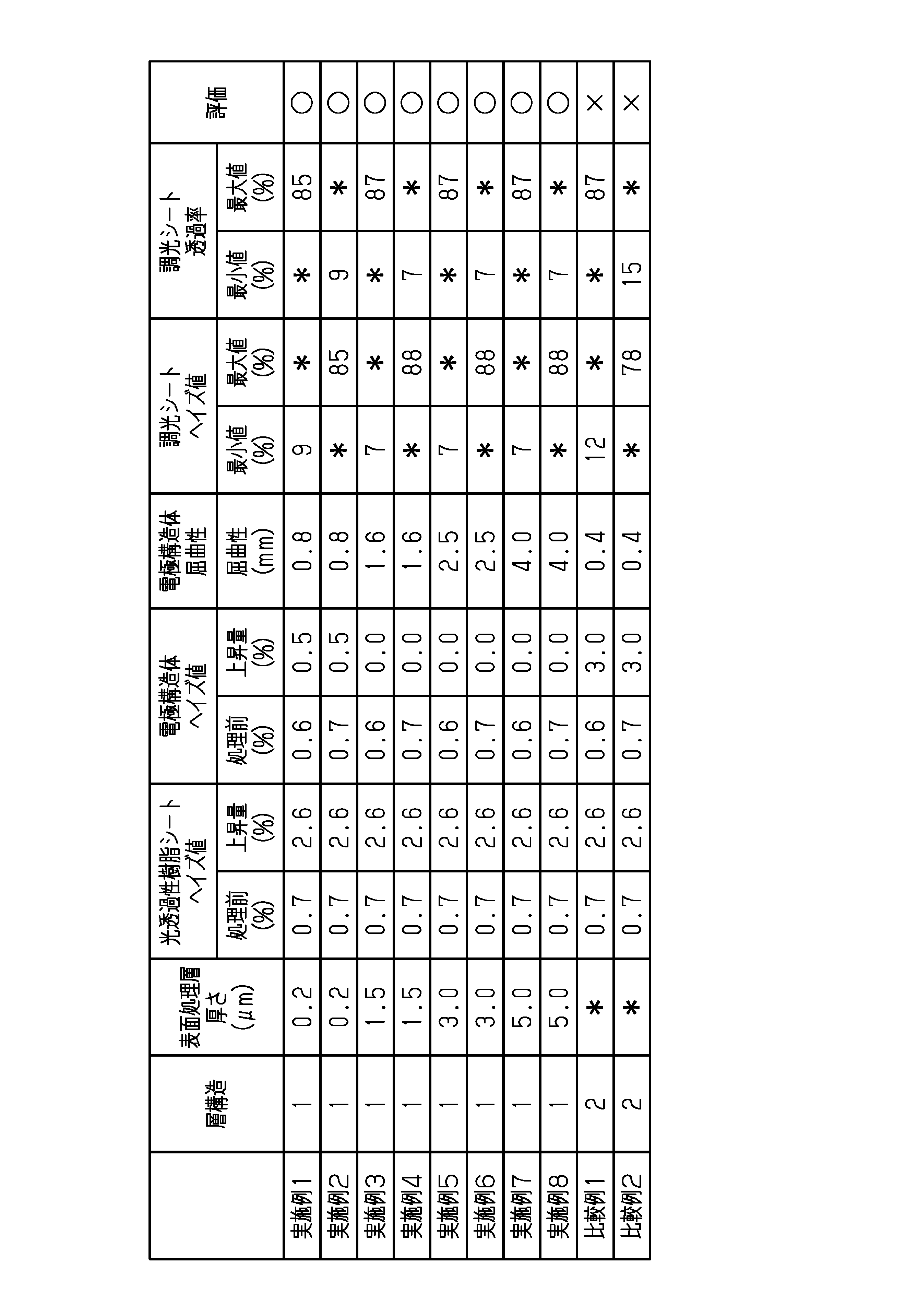
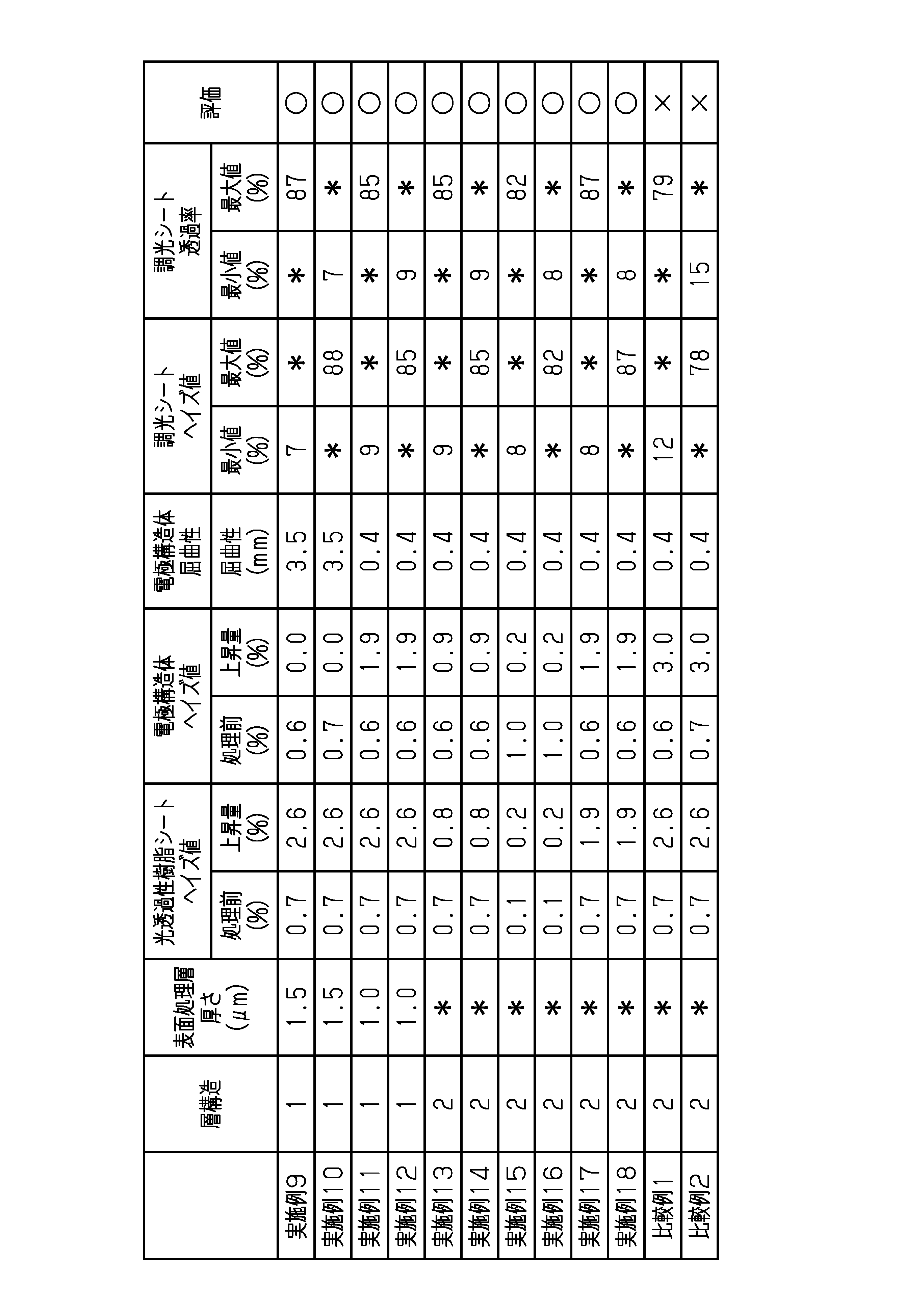
表1,表2が示すように、実施例1~18の電極構造体において、ヘイズ値の上昇量は0.0%以上1.9%以下であり、いずれの水準も条件1を満たすことが認められた。一方、比較例1,2の電極構造体において、ヘイズ値の上昇量は3.0%であり、いずれの水準も条件1を満たしていないことが認められた。また、実施例13~18の光透過性樹脂シートにおいて、ヘイズ値の上昇量は0.2%以上1.9%以下であり、いずれの水準も条件2を満たすことが認められた。
As shown in Tables 1 and 2, in the electrode structures of Examples 1 to 18, the increase in the haze value is 0.0% or more and 1.9% or less, and all levels satisfy the condition 1 Admitted. On the other hand, in the electrode structures of Comparative Examples 1 and 2, the increase in haze value was 3.0%, and it was found that Condition 1 was not satisfied at any level. Further, in the light transmitting resin sheets of Examples 13 to 18, the increase in the haze value was 0.2% or more and 1.9% or less, and it was found that Condition 2 satisfied all levels.
そして、実施例1~18のうち、ノーマル型の調光シートにおいて、ヘイズ値の最小値は7%以上9%以下であり、高温かつ多湿の環境で十分な耐性を有するとする10%以下であることが認められた。また、実施例1~18のうち、リバース型の調光シートにおいて、ヘイズ値の最大値は82%以上88%以下であり、高温かつ多湿の環境で十分な耐性を有するとする80%以上であることが認められた。
And in the normal type light control sheet among Examples 1 to 18, the minimum value of the haze value is 7% or more and 9% or less, and 10% or less which has sufficient resistance in a high temperature and humid environment. It was recognized that there was. In Examples 1 to 18, in the reverse-type light control sheet, the maximum value of the haze value is 82% or more and 88% or less, and 80% or more which has sufficient resistance in a high temperature and humid environment. It was recognized that there was.
また、実施例1~18のうち、ノーマル型の調光シートにおいて、透過率の最大値は82%以上87%以下であり、高温かつ多湿の環境で十分な耐性を有するとする80%以上であることが認められた。また、実施例1~18のうち、リバース型の調光シートにおいて、透過率の最小値は7%以上9%以下であり、高温かつ多湿の環境で十分な耐性を有するとする10%以下であることが認められた。
In addition, in the normal type light control sheet of Examples 1 to 18, the maximum value of the transmittance is 82% or more and 87% or less, and 80% or more which has sufficient resistance in a high temperature and humid environment. It was recognized that there was. In Examples 1 to 18, in the reverse-type light control sheet, the minimum value of the transmittance is 7% to 9%, and 10% or less which has sufficient resistance in a high temperature and humid environment. It was recognized that there was.
これに対して、比較例1の調光シートにおいて、ヘイズ値の最小値は12%であり、透過率の最大値は87%であり、比較例1の調光シートは、ヘイズ値の観点において、高温かつ多湿の環境で十分な耐性を有していないことが認められた。また、比較例2の調光シートにおいて、ヘイズ値の最大値は78%であり、透過率の最小値は15%であり、ヘイズ値および透過率の両観点において、比較例2の調光シートは、高温かつ多湿の環境で十分な耐性を有していないことが認められた。
On the other hand, in the light control sheet of Comparative Example 1, the minimum value of the haze value is 12%, the maximum value of the transmittance is 87%, and the light control sheet of Comparative Example 1 has the viewpoint of the haze value. It has been found that it does not have sufficient resistance in a hot and humid environment. Moreover, in the light control sheet of Comparative Example 2, the maximum value of the haze value is 78%, and the minimum value of the transmittance is 15%. The light control sheet of Comparative Example 2 in both the haze value and the transmittance Were found to be not well tolerated in hot and humid environments.
すなわち、ハードコート層を表面処理層22として備える場合(実施例1~10)、光透過性樹脂シート21が低分子不純物を放出するとしても、液晶分子を用いた配向制御の信頼性を十分に確保することが可能となる。
That is, when the hard coat layer is provided as the surface treatment layer 22 (Examples 1 to 10), even if the light transmitting resin sheet 21 releases low molecular impurities, sufficient reliability of alignment control using liquid crystal molecules is obtained. It becomes possible to secure.
また、拡散抑制層を表面処理層22として備える場合であれ(実施例11~12)、[条件1]を満たす場合であれ(実施例1~18)、同じく、液晶分子を用いた配向制御の信頼性を十分に確保することが可能となる。さらに、[条件2]を満たす場合(実施例13~18)、表面処理層22が割愛された状態で、同じく、液晶分子を用いた配向制御の信頼性を十分に確保することが可能となる。
In addition, if the diffusion suppression layer is provided as the surface treatment layer 22 (Examples 11 to 12) or if [Condition 1] is satisfied (Examples 1 to 18), the alignment control using liquid crystal molecules is also performed similarly. It becomes possible to secure sufficient reliability. Furthermore, when [Condition 2] is satisfied (Examples 13 to 18), in the state where the surface treatment layer 22 is omitted, it is possible to sufficiently ensure the reliability of alignment control using liquid crystal molecules as well. .
なお、実施例1~18の電極構造体においては、屈曲性が0.4mm以上4mm以下であるため、適用される対象の形状に合わせた変形を調光シートで得られることも認められた。
In addition, in the electrode structures of Examples 1 to 18, since the flexibility was 0.4 mm or more and 4 mm or less, it was also recognized that a deformation according to the shape of the object to be applied could be obtained with the light control sheet.
以上説明したように、上記実施形態によれば、以下に列挙する効果が得られる。
(1)表面処理層22を備える場合、低分子不純物が拡散することや、光透過性樹脂シート21で低分子不純物が生成されることが抑えられる。そのため、高温かつ多湿の環境での配向制御の信頼性を向上することが可能となる。
(2)表面処理層22が第1面211に位置する場合には、低分子不純物が調光層30に到達することを、調光層30の直前で抑えることが可能となる。 As described above, according to the above embodiment, the following effects can be obtained.
(1) When thesurface treatment layer 22 is provided, diffusion of low molecular impurities and generation of low molecular impurities in the light transmitting resin sheet 21 can be suppressed. Therefore, it becomes possible to improve the reliability of orientation control in a high temperature and high humidity environment.
(2) When thesurface treatment layer 22 is located on the first surface 211, it is possible to suppress the low molecular impurities from reaching the light control layer 30 immediately before the light control layer 30.
(1)表面処理層22を備える場合、低分子不純物が拡散することや、光透過性樹脂シート21で低分子不純物が生成されることが抑えられる。そのため、高温かつ多湿の環境での配向制御の信頼性を向上することが可能となる。
(2)表面処理層22が第1面211に位置する場合には、低分子不純物が調光層30に到達することを、調光層30の直前で抑えることが可能となる。 As described above, according to the above embodiment, the following effects can be obtained.
(1) When the
(2) When the
(3)表面処理層22が第2面212に位置する場合には、光透過性樹脂シート21での加水分解などによる低分子不純物の生成そのものを抑えることが可能となる。
(3) In the case where the surface treatment layer 22 is located on the second surface 212, it is possible to suppress the generation of low molecular impurities themselves by hydrolysis or the like in the light transmitting resin sheet 21.
(4)表面処理層22が光硬化型樹脂の硬化体や熱硬化型樹脂の硬化体である場合には、硬化型樹脂を硬化するためのエネルギーを、光透過性樹脂シート21を通して供給することが可能ともなる。
(4) When the surface treatment layer 22 is a cured product of a photocurable resin or a cured product of a thermosetting resin, energy for curing the curable resin is supplied through the light transmitting resin sheet 21 Is also possible.
(5)光透過性樹脂シート21と調光層30とを接着する機能を表面処理層22が兼ね備える場合には、光透過性樹脂シート21と調光層30との密着性を高めることが可能ともなる。
(5) When the surface treatment layer 22 has the function of bonding the light transmitting resin sheet 21 and the light control layer 30, the adhesion between the light transmitting resin sheet 21 and the light control layer 30 can be enhanced. It will be.
(6)85℃85%RHの条件下で100時間処理後のヘイズ値の上昇量が、電極構造体において2%未満であるため、調光層30に対する低分子不純物の拡散や生成を抑えることが可能となる。
(6) Since the increase in the haze value after 100 hours of treatment at 85 ° C. and 85% RH is less than 2% in the electrode structure, the diffusion and generation of low molecular impurities to the light control layer 30 are suppressed. Is possible.
(7)さらに、85℃85%RHの条件下で100時間処理後のヘイズ値の上昇量が、光透過性樹脂シート21において2%未満である場合には、(6)に準じた効果を高めることが可能であり、また、表面処理層22を割愛することも可能となる。
(7) Further, when the increase in haze value after 100 hours of treatment at 85 ° C. and 85% RH is less than 2% in the light transmitting resin sheet 21, the effect according to (6) is obtained. The surface treatment layer 22 can also be omitted.
(8)導電性ポリマーからなる電極層31は、通常、導電性金属酸化物と比べて、低分子不純物を透過しやすい一方で、優れた可撓性を有する。それゆえに、電極層31が導電性ポリマーからなる場合には、高温かつ多湿の環境での配向制御の信頼性を向上し、かつ、可撓性に優れた調光シート10を提供することが可能ともなる。
(8) The electrode layer 31 made of a conductive polymer usually has excellent flexibility while transmitting low molecular impurities more easily than conductive metal oxides. Therefore, when the electrode layer 31 is made of a conductive polymer, it is possible to improve the reliability of orientation control in a high temperature and humidity environment and provide the light control sheet 10 excellent in flexibility. It will be.
なお、上述した実施形態は、以下のように適宜変更して実施することができる。
[液晶層32]
・液晶層32の型式は、高分子分散型液晶(PDLC:Polymer Dispersed Liquid Crystal)、あるいは、カプセル型ネマティック液晶(NCAP:Nematic Curvilinear Aligned Phase)に変更できる。高分子分散型液晶は、孤立した多数の空隙を高分子層のなかに備え、高分子層に分散した各空隙のなかに液晶組成物を保持する。カプセル型ネマティック液晶は、カプセル状を有した液晶組成物を高分子層のなかに保持する。 The embodiment described above can be implemented with appropriate modifications as follows.
[Liquid crystal layer 32]
The type of theliquid crystal layer 32 can be changed to polymer dispersed liquid crystal (PDLC) or capsule-type nematic liquid crystal (NCAP). The polymer dispersed liquid crystal has a large number of isolated voids in the polymer layer, and holds the liquid crystal composition in the voids dispersed in the polymer layer. The capsule nematic liquid crystal holds the liquid crystal composition having a capsule shape in the polymer layer.
[液晶層32]
・液晶層32の型式は、高分子分散型液晶(PDLC:Polymer Dispersed Liquid Crystal)、あるいは、カプセル型ネマティック液晶(NCAP:Nematic Curvilinear Aligned Phase)に変更できる。高分子分散型液晶は、孤立した多数の空隙を高分子層のなかに備え、高分子層に分散した各空隙のなかに液晶組成物を保持する。カプセル型ネマティック液晶は、カプセル状を有した液晶組成物を高分子層のなかに保持する。 The embodiment described above can be implemented with appropriate modifications as follows.
[Liquid crystal layer 32]
The type of the
[調光シートの層構造]
・調光シートが備える一方の光透過性樹脂基材20を、上述した第1層構造に準じた構造とし、他方の光透過性樹脂基材を、上述した第2層構造に準じた構造とすることも可能である。すなわち、一方の光透過性樹脂基材20が、表面処理層22を備え、他方の光透過性樹脂基材20が、条件2を満たす光透過性樹脂シート21のみから構成されてもよい。 [Layer structure of light control sheet]
-One light transmittingresin substrate 20 included in the light control sheet has a structure according to the first layer structure described above, and the other light transmitting resin substrate has a structure according to the second layer structure described above It is also possible. That is, one light transmitting resin base material 20 may be provided with the surface treatment layer 22, and the other light transmitting resin base material 20 may be constituted only by the light transmitting resin sheet 21 satisfying the condition 2.
・調光シートが備える一方の光透過性樹脂基材20を、上述した第1層構造に準じた構造とし、他方の光透過性樹脂基材を、上述した第2層構造に準じた構造とすることも可能である。すなわち、一方の光透過性樹脂基材20が、表面処理層22を備え、他方の光透過性樹脂基材20が、条件2を満たす光透過性樹脂シート21のみから構成されてもよい。 [Layer structure of light control sheet]
-One light transmitting
Claims (12)
- 光透過性樹脂基材と、
前記光透過性樹脂基材に支持される調光層と、を備え、
前記調光層は、液晶層と、前記液晶層を挟む一対の電極層と、を備え、
前記光透過性樹脂基材は、
前記調光層と対向する第1面と、前記第1面とは反対側の面である第2面とを備える光透過性樹脂シートと、
前記第1面および前記第2面の少なくとも一方に位置し、バリア性を有した表面処理層と、を備える
調光シート。 A light transmitting resin base material,
And a light control layer supported by the light transmitting resin base material,
The light control layer includes a liquid crystal layer and a pair of electrode layers sandwiching the liquid crystal layer,
The light transmitting resin base material is
A light transmitting resin sheet comprising a first surface facing the light control layer, and a second surface opposite to the first surface;
A light control sheet comprising: a surface treatment layer located on at least one of the first surface and the second surface and having a barrier property. - 前記表面処理層は、ハードコート層である
請求項1に記載の調光シート。 The light control sheet according to claim 1, wherein the surface treatment layer is a hard coat layer. - 前記ハードコート層は、光硬化型樹脂の硬化体または熱硬化型樹脂の硬化体である
請求項2に記載の調光シート。 The light control sheet according to claim 2, wherein the hard coat layer is a cured product of a photocurable resin or a cured product of a thermosetting resin. - 前記表面処理層は、前記光透過性樹脂シートから低分子不純物が拡散することを抑制する拡散抑制層である
請求項1に記載の調光シート。 The light control sheet according to claim 1, wherein the surface treatment layer is a diffusion suppression layer that suppresses the diffusion of low molecular impurities from the light transmitting resin sheet. - 前記拡散抑制層は、アクリル系ポリマー、ポリエステル、ポリウレタン、および、ポリビニルアルコールからなる群から選ばれる一種以上のポリマーを含む組成物の架橋体であり、かつ、前記ポリマーは、架橋構造を形成する官能基を有する
請求項4に記載の調光シート。 The diffusion suppression layer is a cross-linked body of a composition containing one or more polymers selected from the group consisting of acrylic polymers, polyesters, polyurethanes, and polyvinyl alcohols, and the polymers have a functional group forming a cross-linked structure. The light control sheet according to claim 4 having a base. - 光透過性樹脂基材と、
前記光透過性樹脂基材に支持される調光層と、を備え、
前記調光層は、液晶層と、前記液晶層を挟む電極層と、を備え、
前記電極層と、前記電極層と接合した前記光透過性樹脂基材とからなる構造体において、温度が85℃かつ相対湿度が85%の条件下で100時間処理後のヘイズ値の上昇量が2%未満である
調光シート。 A light transmitting resin base material,
And a light control layer supported by the light transmitting resin base material,
The light control layer includes a liquid crystal layer and an electrode layer sandwiching the liquid crystal layer,
In the structure composed of the electrode layer and the light transmitting resin base joined to the electrode layer, the increase in the haze value after 100 hours of treatment under the conditions of a temperature of 85 ° C. and a relative humidity of 85% Light control sheet which is less than 2%. - 前記光透過性樹脂基材は、
前記調光層と対向する第1面と、前記第1面とは反対側の面である第2面とを備える光透過性樹脂シートと、
前記第1面および前記第2面の少なくとも一方に位置し、バリア性を有した表面処理層と、を備える
請求項6に記載の調光シート。 The light transmitting resin base material is
A light transmitting resin sheet comprising a first surface facing the light control layer, and a second surface opposite to the first surface;
The light control sheet according to claim 6, comprising: a surface treatment layer located on at least one of the first surface and the second surface and having a barrier property. - 前記光透過性樹脂基材において、温度が85℃かつ相対湿度が85%の条件下で100時間処理後のヘイズ値の上昇量が2%未満である
請求項6または7に記載の調光シート。 The light control sheet according to claim 6 or 7, wherein the increase in haze value after 100 hours of treatment under the conditions of a temperature of 85 ° C and a relative humidity of 85% is less than 2% in the light transmitting resin base material. . - 前記光透過性樹脂基材は、ポリエチレンナフタレートシート、または、ポリイミドシートである
請求項6から8のいずれか一項に記載の調光シート。 The light control sheet according to any one of claims 6 to 8, wherein the light transmitting resin substrate is a polyethylene naphthalate sheet or a polyimide sheet. - 前記電極層は、導電性ポリマーから形成される
請求項1から9のいずれか一項に記載の調光シート。 The light control sheet according to any one of claims 1 to 9, wherein the electrode layer is formed of a conductive polymer. - 前記液晶層は、複数のドメインを区画するポリマーネットワークと、各ドメインを埋める液晶組成物とを備える
請求項1から10のいずれか一項に記載の調光シート。 The light control sheet according to any one of claims 1 to 10, wherein the liquid crystal layer includes a polymer network that defines a plurality of domains, and a liquid crystal composition that fills each of the domains. - 請求項1から11のいずれか一項に記載の調光シートと、
前記調光シートが備える電極層に対する駆動電圧の印加を制御する電圧制御部と、を備える
調光装置。 The light control sheet according to any one of claims 1 to 11,
And a voltage control unit configured to control application of a drive voltage to an electrode layer included in the light control sheet.
Priority Applications (3)
| Application Number | Priority Date | Filing Date | Title |
|---|---|---|---|
| CN201880085771.1A CN111566550B (en) | 2018-01-12 | 2018-12-20 | Dimming sheet and dimming device |
| EP18900272.8A EP3739377A4 (en) | 2018-01-12 | 2018-12-20 | Light control sheet and light control device |
| US16/925,591 US11281063B2 (en) | 2018-01-12 | 2020-07-10 | Light control sheet and light control device |
Applications Claiming Priority (2)
| Application Number | Priority Date | Filing Date | Title |
|---|---|---|---|
| JP2018003726A JP6447757B1 (en) | 2018-01-12 | 2018-01-12 | Light control sheet and light control device |
| JP2018-003726 | 2018-02-23 |
Related Child Applications (1)
| Application Number | Title | Priority Date | Filing Date |
|---|---|---|---|
| US16/925,591 Continuation US11281063B2 (en) | 2018-01-12 | 2020-07-10 | Light control sheet and light control device |
Publications (1)
| Publication Number | Publication Date |
|---|---|
| WO2019138832A1 true WO2019138832A1 (en) | 2019-07-18 |
Family
ID=64960219
Family Applications (1)
| Application Number | Title | Priority Date | Filing Date |
|---|---|---|---|
| PCT/JP2018/046991 WO2019138832A1 (en) | 2018-01-12 | 2018-12-20 | Light control sheet and light control device |
Country Status (5)
| Country | Link |
|---|---|
| US (1) | US11281063B2 (en) |
| EP (1) | EP3739377A4 (en) |
| JP (1) | JP6447757B1 (en) |
| CN (1) | CN111566550B (en) |
| WO (1) | WO2019138832A1 (en) |
Families Citing this family (2)
| Publication number | Priority date | Publication date | Assignee | Title |
|---|---|---|---|---|
| JP7327078B2 (en) * | 2019-10-23 | 2023-08-16 | 大日本印刷株式会社 | Design material and manufacturing method of design material |
| JP7360626B2 (en) | 2020-01-29 | 2023-10-13 | 大日本印刷株式会社 | A light control unit, a light control member including the light control unit, and a moving object including the light control member |
Citations (7)
| Publication number | Priority date | Publication date | Assignee | Title |
|---|---|---|---|---|
| JPH02208627A (en) * | 1989-02-08 | 1990-08-20 | Teijin Ltd | Light control film |
| JPH06234182A (en) * | 1992-10-13 | 1994-08-23 | Afuiniteii Kk | Ultraviolet cutting laminated body and window using it |
| JP2003512647A (en) * | 1999-10-15 | 2003-04-02 | アグフア−ゲヴエルト,ナームローゼ・フエンノートシヤツプ | Liquid crystal alignment layer |
| WO2009102079A1 (en) * | 2008-02-13 | 2009-08-20 | Sumitomo Metal Mining Co., Ltd. | Flexible transparent conductive film, flexible functional element, and methods for manufacturing them |
| WO2010100807A1 (en) * | 2009-03-02 | 2010-09-10 | 九州ナノテック光学株式会社 | Liquid-crystal blind device and method of using same |
| WO2016072498A1 (en) | 2014-11-07 | 2016-05-12 | 日産化学工業株式会社 | Liquid crystal display element |
| JP2016110148A (en) * | 2014-12-05 | 2016-06-20 | 三菱化学株式会社 | Liquid crystal element, liquid crystal composition, screen and display using liquid crystal element |
Family Cites Families (12)
| Publication number | Priority date | Publication date | Assignee | Title |
|---|---|---|---|---|
| DE69729022T2 (en) * | 1996-03-25 | 2005-06-09 | Teijin Ltd. | Coating composition, transparent electrode substrate with such a coating and liquid crystal display element with such a substrate |
| US7357965B1 (en) | 1999-10-15 | 2008-04-15 | Agfa-Gevaert, N.V. | Liquid crystal alignment layer |
| JP2004198505A (en) * | 2002-12-16 | 2004-07-15 | Sony Corp | Dimmer and method for driving the same, and image pickup device |
| CN102137884B (en) * | 2008-06-30 | 2014-06-25 | 可隆工业株式会社 | Plastic substrate and device including the same |
| CN201331646Y (en) * | 2009-01-08 | 2009-10-21 | 北京众智同辉科技有限公司 | Electro-liquid crystal atomizing glass with water-proof structure |
| CN102576108A (en) * | 2009-08-10 | 2012-07-11 | 吉坤日矿日石能源株式会社 | Liquid-crystal film and optical element obtained using same |
| US20170003525A1 (en) * | 2014-01-24 | 2017-01-05 | Dai Nippon Printing Co., Ltd. | Light controlling sheet and light controlling plate |
| JP2016207041A (en) | 2015-04-24 | 2016-12-08 | 株式会社ダイセル | Transparent Conductive Laminate and Method for Producing the Same |
| JP6037070B1 (en) * | 2016-02-22 | 2016-11-30 | 大日本印刷株式会社 | Dimming cell |
| ES2831103T3 (en) * | 2016-02-26 | 2021-06-07 | Nissan Chemical Corp | Liquid crystal display device |
| JP6888431B2 (en) * | 2016-06-10 | 2021-06-16 | 凸版印刷株式会社 | Projection screen and image display system |
| KR101801471B1 (en) * | 2016-06-23 | 2017-11-24 | 동우 화인켐 주식회사 | Hard Coating Film and Image Display Device Using the Same |
-
2018
- 2018-01-12 JP JP2018003726A patent/JP6447757B1/en active Active
- 2018-12-20 WO PCT/JP2018/046991 patent/WO2019138832A1/en unknown
- 2018-12-20 CN CN201880085771.1A patent/CN111566550B/en active Active
- 2018-12-20 EP EP18900272.8A patent/EP3739377A4/en active Pending
-
2020
- 2020-07-10 US US16/925,591 patent/US11281063B2/en active Active
Patent Citations (7)
| Publication number | Priority date | Publication date | Assignee | Title |
|---|---|---|---|---|
| JPH02208627A (en) * | 1989-02-08 | 1990-08-20 | Teijin Ltd | Light control film |
| JPH06234182A (en) * | 1992-10-13 | 1994-08-23 | Afuiniteii Kk | Ultraviolet cutting laminated body and window using it |
| JP2003512647A (en) * | 1999-10-15 | 2003-04-02 | アグフア−ゲヴエルト,ナームローゼ・フエンノートシヤツプ | Liquid crystal alignment layer |
| WO2009102079A1 (en) * | 2008-02-13 | 2009-08-20 | Sumitomo Metal Mining Co., Ltd. | Flexible transparent conductive film, flexible functional element, and methods for manufacturing them |
| WO2010100807A1 (en) * | 2009-03-02 | 2010-09-10 | 九州ナノテック光学株式会社 | Liquid-crystal blind device and method of using same |
| WO2016072498A1 (en) | 2014-11-07 | 2016-05-12 | 日産化学工業株式会社 | Liquid crystal display element |
| JP2016110148A (en) * | 2014-12-05 | 2016-06-20 | 三菱化学株式会社 | Liquid crystal element, liquid crystal composition, screen and display using liquid crystal element |
Also Published As
| Publication number | Publication date |
|---|---|
| CN111566550A (en) | 2020-08-21 |
| CN111566550B (en) | 2023-10-31 |
| EP3739377A1 (en) | 2020-11-18 |
| US11281063B2 (en) | 2022-03-22 |
| JP6447757B1 (en) | 2019-01-09 |
| US20200341303A1 (en) | 2020-10-29 |
| EP3739377A4 (en) | 2021-03-03 |
| JP2019124759A (en) | 2019-07-25 |
Similar Documents
| Publication | Publication Date | Title |
|---|---|---|
| JP4479608B2 (en) | Transparent conductor and panel switch | |
| JP5838152B2 (en) | Functional laminate, transparent conductive laminate for touch panel, and touch panel using the same | |
| JP5173408B2 (en) | Method for laminating thin films for SPD light valves and SPD light valves incorporating the laminated thin films | |
| JP5158112B2 (en) | Transparent conductive material and touch panel | |
| CN104854647A (en) | Packaging film for display device | |
| JP7279608B2 (en) | Light control film and light control device | |
| WO2019138832A1 (en) | Light control sheet and light control device | |
| TWI746765B (en) | Optical laminate | |
| JP2020027210A (en) | Design material and method for manufacturing laminated polymer dispersion type liquid crystal device used for the same | |
| US20210403769A1 (en) | Transfer foil for touch sensor and method for manufacturing conductive film for touch sensor | |
| JP7067446B2 (en) | Dimming sheet and dimming device | |
| JP6173726B2 (en) | Method for producing multilayer laminated film | |
| JP6031382B2 (en) | Method for producing multilayer laminated film | |
| JP2018060060A (en) | Polarizing plate and liquid crystal display device | |
| JP6477654B2 (en) | Light control film | |
| WO2021201275A1 (en) | Laminated glass | |
| JP7326733B2 (en) | Light control film, light control device | |
| JP6216523B2 (en) | Method for producing multilayer laminated film | |
| CN210605296U (en) | Liquid crystal writing board | |
| JP7133142B2 (en) | Light control unit, light control component | |
| JP6040081B2 (en) | Method for producing transparent conductive laminate | |
| JP2021039382A (en) | Dimmer | |
| JP2011170278A (en) | Light-scattering type liquid crystal sheet, liquid crystal display sheet and liquid crystal display device | |
| JP2016190758A (en) | Glass laminate and light control component for the same | |
| JP7279346B2 (en) | Light control film, light control device |
Legal Events
| Date | Code | Title | Description |
|---|---|---|---|
| 121 | Ep: the epo has been informed by wipo that ep was designated in this application |
Ref document number: 18900272 Country of ref document: EP Kind code of ref document: A1 |
|
| NENP | Non-entry into the national phase |
Ref country code: DE |
|
| ENP | Entry into the national phase |
Ref document number: 2018900272 Country of ref document: EP Effective date: 20200812 |