WO2019132242A1 - Plaque polarisante et dispositif d'affichage optique la comprenant - Google Patents
Plaque polarisante et dispositif d'affichage optique la comprenant Download PDFInfo
- Publication number
- WO2019132242A1 WO2019132242A1 PCT/KR2018/013910 KR2018013910W WO2019132242A1 WO 2019132242 A1 WO2019132242 A1 WO 2019132242A1 KR 2018013910 W KR2018013910 W KR 2018013910W WO 2019132242 A1 WO2019132242 A1 WO 2019132242A1
- Authority
- WO
- WIPO (PCT)
- Prior art keywords
- light
- polarizing plate
- shielding layer
- polarizer
- absorber
- Prior art date
Links
- 230000003287 optical effect Effects 0.000 title claims abstract description 17
- 239000010410 layer Substances 0.000 claims abstract description 249
- 239000006096 absorbing agent Substances 0.000 claims abstract description 66
- 239000012790 adhesive layer Substances 0.000 claims abstract description 43
- 230000001681 protective effect Effects 0.000 claims description 54
- 239000000203 mixture Substances 0.000 claims description 32
- 230000008859 change Effects 0.000 claims description 29
- 239000000853 adhesive Substances 0.000 claims description 20
- 230000001070 adhesive effect Effects 0.000 claims description 20
- 150000001875 compounds Chemical class 0.000 claims description 20
- 239000012963 UV stabilizer Substances 0.000 claims description 18
- 239000000049 pigment Substances 0.000 claims description 18
- -1 metal complex salt Chemical class 0.000 claims description 15
- 229920001187 thermosetting polymer Polymers 0.000 claims description 15
- JYEUMXHLPRZUAT-UHFFFAOYSA-N 1,2,3-triazine Chemical compound C1=CN=NN=C1 JYEUMXHLPRZUAT-UHFFFAOYSA-N 0.000 claims description 12
- 125000000217 alkyl group Chemical group 0.000 claims description 12
- RWCCWEUUXYIKHB-UHFFFAOYSA-N benzophenone Chemical group C=1C=CC=CC=1C(=O)C1=CC=CC=C1 RWCCWEUUXYIKHB-UHFFFAOYSA-N 0.000 claims description 12
- 239000012965 benzophenone Substances 0.000 claims description 12
- 239000011230 binding agent Substances 0.000 claims description 11
- 125000004432 carbon atom Chemical group C* 0.000 claims description 11
- 229920005989 resin Polymers 0.000 claims description 11
- 239000011347 resin Substances 0.000 claims description 11
- 239000003999 initiator Substances 0.000 claims description 10
- HPJFXFRNEJHDFR-UHFFFAOYSA-N 22291-04-9 Chemical compound C1=CC(C(N(CCN(C)C)C2=O)=O)=C3C2=CC=C2C(=O)N(CCN(C)C)C(=O)C1=C32 HPJFXFRNEJHDFR-UHFFFAOYSA-N 0.000 claims description 6
- 239000004925 Acrylic resin Substances 0.000 claims description 6
- 238000010521 absorption reaction Methods 0.000 claims description 6
- 230000001678 irradiating effect Effects 0.000 claims description 6
- ZQBAKBUEJOMQEX-UHFFFAOYSA-N phenyl salicylate Chemical compound OC1=CC=CC=C1C(=O)OC1=CC=CC=C1 ZQBAKBUEJOMQEX-UHFFFAOYSA-N 0.000 claims description 6
- 229920000178 Acrylic resin Polymers 0.000 claims description 5
- 125000003545 alkoxy group Chemical group 0.000 claims description 5
- 239000006229 carbon black Substances 0.000 claims description 5
- 125000002887 hydroxy group Chemical group [H]O* 0.000 claims description 5
- 229920005749 polyurethane resin Polymers 0.000 claims description 5
- QRUDEWIWKLJBPS-UHFFFAOYSA-N benzotriazole Chemical compound C1=CC=C2N[N][N]C2=C1 QRUDEWIWKLJBPS-UHFFFAOYSA-N 0.000 claims description 4
- 239000012964 benzotriazole Substances 0.000 claims description 4
- 229920001721 polyimide Polymers 0.000 claims description 4
- VMRIVYANZGSGRV-UHFFFAOYSA-N 4-phenyl-2h-triazin-5-one Chemical compound OC1=CN=NN=C1C1=CC=CC=C1 VMRIVYANZGSGRV-UHFFFAOYSA-N 0.000 claims description 3
- 229920001651 Cyanoacrylate Polymers 0.000 claims description 3
- MWCLLHOVUTZFKS-UHFFFAOYSA-N Methyl cyanoacrylate Chemical compound COC(=O)C(=C)C#N MWCLLHOVUTZFKS-UHFFFAOYSA-N 0.000 claims description 3
- QCEUXSAXTBNJGO-UHFFFAOYSA-N [Ag].[Sn] Chemical compound [Ag].[Sn] QCEUXSAXTBNJGO-UHFFFAOYSA-N 0.000 claims description 3
- 239000000956 alloy Substances 0.000 claims description 3
- 229910045601 alloy Inorganic materials 0.000 claims description 3
- 150000001412 amines Chemical class 0.000 claims description 3
- 125000005843 halogen group Chemical group 0.000 claims description 3
- FTWUXYZHDFCGSV-UHFFFAOYSA-N n,n'-diphenyloxamide Chemical compound C=1C=CC=CC=1NC(=O)C(=O)NC1=CC=CC=C1 FTWUXYZHDFCGSV-UHFFFAOYSA-N 0.000 claims description 3
- 229960000969 phenyl salicylate Drugs 0.000 claims description 3
- 239000009719 polyimide resin Substances 0.000 claims description 3
- YGSDEFSMJLZEOE-UHFFFAOYSA-M salicylate Chemical compound OC1=CC=CC=C1C([O-])=O YGSDEFSMJLZEOE-UHFFFAOYSA-M 0.000 claims description 3
- 229960001860 salicylate Drugs 0.000 claims description 3
- 229940114081 cinnamate Drugs 0.000 claims description 2
- WBYWAXJHAXSJNI-VOTSOKGWSA-M trans-cinnamate Chemical compound [O-]C(=O)\C=C\C1=CC=CC=C1 WBYWAXJHAXSJNI-VOTSOKGWSA-M 0.000 claims description 2
- 238000009281 ultraviolet germicidal irradiation Methods 0.000 description 17
- 230000000694 effects Effects 0.000 description 14
- 230000007774 longterm Effects 0.000 description 12
- 229910052739 hydrogen Inorganic materials 0.000 description 11
- 239000001257 hydrogen Substances 0.000 description 11
- 230000000052 comparative effect Effects 0.000 description 9
- NIXOWILDQLNWCW-UHFFFAOYSA-M Acrylate Chemical compound [O-]C(=O)C=C NIXOWILDQLNWCW-UHFFFAOYSA-M 0.000 description 8
- UFHFLCQGNIYNRP-UHFFFAOYSA-N Hydrogen Chemical compound [H][H] UFHFLCQGNIYNRP-UHFFFAOYSA-N 0.000 description 8
- 238000004519 manufacturing process Methods 0.000 description 8
- 239000002904 solvent Substances 0.000 description 8
- SIKJAQJRHWYJAI-UHFFFAOYSA-N Indole Chemical compound C1=CC=C2NC=CC2=C1 SIKJAQJRHWYJAI-UHFFFAOYSA-N 0.000 description 7
- 125000003342 alkenyl group Chemical group 0.000 description 7
- 239000006185 dispersion Substances 0.000 description 6
- 229910052736 halogen Inorganic materials 0.000 description 6
- 150000002367 halogens Chemical class 0.000 description 6
- 125000003118 aryl group Chemical group 0.000 description 5
- 238000001723 curing Methods 0.000 description 5
- 125000001072 heteroaryl group Chemical group 0.000 description 5
- 229920000139 polyethylene terephthalate Polymers 0.000 description 5
- 239000005020 polyethylene terephthalate Substances 0.000 description 5
- 125000000008 (C1-C10) alkyl group Chemical group 0.000 description 4
- 229920002799 BoPET Polymers 0.000 description 4
- 239000004372 Polyvinyl alcohol Substances 0.000 description 4
- 125000003277 amino group Chemical group 0.000 description 4
- 229920001577 copolymer Polymers 0.000 description 4
- 125000004093 cyano group Chemical group *C#N 0.000 description 4
- 229920002451 polyvinyl alcohol Polymers 0.000 description 4
- ZWEHNKRNPOVVGH-UHFFFAOYSA-N 2-Butanone Chemical compound CCC(C)=O ZWEHNKRNPOVVGH-UHFFFAOYSA-N 0.000 description 3
- OKTJSMMVPCPJKN-UHFFFAOYSA-N Carbon Chemical compound [C] OKTJSMMVPCPJKN-UHFFFAOYSA-N 0.000 description 3
- 229920000089 Cyclic olefin copolymer Polymers 0.000 description 3
- CERQOIWHTDAKMF-UHFFFAOYSA-N Methacrylic acid Chemical compound CC(=C)C(O)=O CERQOIWHTDAKMF-UHFFFAOYSA-N 0.000 description 3
- 239000006087 Silane Coupling Agent Substances 0.000 description 3
- PPBRXRYQALVLMV-UHFFFAOYSA-N Styrene Natural products C=CC1=CC=CC=C1 PPBRXRYQALVLMV-UHFFFAOYSA-N 0.000 description 3
- 238000002835 absorbance Methods 0.000 description 3
- NIXOWILDQLNWCW-UHFFFAOYSA-N acrylic acid group Chemical group C(C=C)(=O)O NIXOWILDQLNWCW-UHFFFAOYSA-N 0.000 description 3
- 125000004453 alkoxycarbonyl group Chemical group 0.000 description 3
- 230000000903 blocking effect Effects 0.000 description 3
- 150000002431 hydrogen Chemical class 0.000 description 3
- PZOUSPYUWWUPPK-UHFFFAOYSA-N indole Natural products CC1=CC=CC2=C1C=CN2 PZOUSPYUWWUPPK-UHFFFAOYSA-N 0.000 description 3
- RKJUIXBNRJVNHR-UHFFFAOYSA-N indolenine Natural products C1=CC=C2CC=NC2=C1 RKJUIXBNRJVNHR-UHFFFAOYSA-N 0.000 description 3
- RRQYJINTUHWNHW-UHFFFAOYSA-N 1-ethoxy-2-(2-ethoxyethoxy)ethane Chemical compound CCOCCOCCOCC RRQYJINTUHWNHW-UHFFFAOYSA-N 0.000 description 2
- ARXJGSRGQADJSQ-UHFFFAOYSA-N 1-methoxypropan-2-ol Chemical compound COCC(C)O ARXJGSRGQADJSQ-UHFFFAOYSA-N 0.000 description 2
- LEJBBGNFPAFPKQ-UHFFFAOYSA-N 2-(2-prop-2-enoyloxyethoxy)ethyl prop-2-enoate Chemical compound C=CC(=O)OCCOCCOC(=O)C=C LEJBBGNFPAFPKQ-UHFFFAOYSA-N 0.000 description 2
- XNWFRZJHXBZDAG-UHFFFAOYSA-N 2-METHOXYETHANOL Chemical compound COCCO XNWFRZJHXBZDAG-UHFFFAOYSA-N 0.000 description 2
- INQDDHNZXOAFFD-UHFFFAOYSA-N 2-[2-(2-prop-2-enoyloxyethoxy)ethoxy]ethyl prop-2-enoate Chemical compound C=CC(=O)OCCOCCOCCOC(=O)C=C INQDDHNZXOAFFD-UHFFFAOYSA-N 0.000 description 2
- TXBCBTDQIULDIA-UHFFFAOYSA-N 2-[[3-hydroxy-2,2-bis(hydroxymethyl)propoxy]methyl]-2-(hydroxymethyl)propane-1,3-diol Chemical compound OCC(CO)(CO)COCC(CO)(CO)CO TXBCBTDQIULDIA-UHFFFAOYSA-N 0.000 description 2
- XLLIQLLCWZCATF-UHFFFAOYSA-N 2-methoxyethyl acetate Chemical compound COCCOC(C)=O XLLIQLLCWZCATF-UHFFFAOYSA-N 0.000 description 2
- KUDUQBURMYMBIJ-UHFFFAOYSA-N 2-prop-2-enoyloxyethyl prop-2-enoate Chemical compound C=CC(=O)OCCOC(=O)C=C KUDUQBURMYMBIJ-UHFFFAOYSA-N 0.000 description 2
- 239000004593 Epoxy Substances 0.000 description 2
- ZRALSGWEFCBTJO-UHFFFAOYSA-N Guanidine Chemical compound NC(N)=N ZRALSGWEFCBTJO-UHFFFAOYSA-N 0.000 description 2
- 239000004820 Pressure-sensitive adhesive Substances 0.000 description 2
- 239000000654 additive Substances 0.000 description 2
- 229920006223 adhesive resin Polymers 0.000 description 2
- 125000001931 aliphatic group Chemical group 0.000 description 2
- 239000007864 aqueous solution Substances 0.000 description 2
- 125000003710 aryl alkyl group Chemical group 0.000 description 2
- AOJOEFVRHOZDFN-UHFFFAOYSA-N benzyl 2-methylprop-2-enoate Chemical compound CC(=C)C(=O)OCC1=CC=CC=C1 AOJOEFVRHOZDFN-UHFFFAOYSA-N 0.000 description 2
- 230000015572 biosynthetic process Effects 0.000 description 2
- IISBACLAFKSPIT-UHFFFAOYSA-N bisphenol A Chemical compound C=1C=C(O)C=CC=1C(C)(C)C1=CC=C(O)C=C1 IISBACLAFKSPIT-UHFFFAOYSA-N 0.000 description 2
- 238000005336 cracking Methods 0.000 description 2
- 238000007756 gravure coating Methods 0.000 description 2
- 125000004435 hydrogen atom Chemical group [H]* 0.000 description 2
- 239000002346 layers by function Substances 0.000 description 2
- 239000004973 liquid crystal related substance Substances 0.000 description 2
- 229910052751 metal Inorganic materials 0.000 description 2
- 239000002184 metal Substances 0.000 description 2
- 238000000034 method Methods 0.000 description 2
- 239000000178 monomer Substances 0.000 description 2
- DNIAPMSPPWPWGF-UHFFFAOYSA-N monopropylene glycol Natural products CC(O)CO DNIAPMSPPWPWGF-UHFFFAOYSA-N 0.000 description 2
- WXZMFSXDPGVJKK-UHFFFAOYSA-N pentaerythritol Chemical compound OCC(CO)(CO)CO WXZMFSXDPGVJKK-UHFFFAOYSA-N 0.000 description 2
- 125000001997 phenyl group Chemical group [H]C1=C([H])C([H])=C(*)C([H])=C1[H] 0.000 description 2
- LLHKCFNBLRBOGN-UHFFFAOYSA-N propylene glycol methyl ether acetate Chemical compound COCC(C)OC(C)=O LLHKCFNBLRBOGN-UHFFFAOYSA-N 0.000 description 2
- 150000003254 radicals Chemical class 0.000 description 2
- 238000001029 thermal curing Methods 0.000 description 2
- NLEAEGDBKRBJAP-UHFFFAOYSA-N (1-methylimidazol-4-yl)methanol Chemical compound CN1C=NC(CO)=C1 NLEAEGDBKRBJAP-UHFFFAOYSA-N 0.000 description 1
- KMOUUZVZFBCRAM-OLQVQODUSA-N (3as,7ar)-3a,4,7,7a-tetrahydro-2-benzofuran-1,3-dione Chemical compound C1C=CC[C@@H]2C(=O)OC(=O)[C@@H]21 KMOUUZVZFBCRAM-OLQVQODUSA-N 0.000 description 1
- 125000006376 (C3-C10) cycloalkyl group Chemical group 0.000 description 1
- QNRATNLHPGXHMA-XZHTYLCXSA-N (r)-(6-ethoxyquinolin-4-yl)-[(2s,4s,5r)-5-ethyl-1-azabicyclo[2.2.2]octan-2-yl]methanol;hydrochloride Chemical compound Cl.C([C@H]([C@H](C1)CC)C2)CN1[C@@H]2[C@H](O)C1=CC=NC2=CC=C(OCC)C=C21 QNRATNLHPGXHMA-XZHTYLCXSA-N 0.000 description 1
- LZDKZFUFMNSQCJ-UHFFFAOYSA-N 1,2-diethoxyethane Chemical compound CCOCCOCC LZDKZFUFMNSQCJ-UHFFFAOYSA-N 0.000 description 1
- QLGYTJLZFZUDFL-UHFFFAOYSA-N 1,3-bis[1-(1h-imidazol-2-yl)propyl]urea Chemical compound N=1C=CNC=1C(CC)NC(=O)NC(CC)C1=NC=CN1 QLGYTJLZFZUDFL-UHFFFAOYSA-N 0.000 description 1
- CNJRPYFBORAQAU-UHFFFAOYSA-N 1-ethoxy-2-(2-methoxyethoxy)ethane Chemical compound CCOCCOCCOC CNJRPYFBORAQAU-UHFFFAOYSA-N 0.000 description 1
- DMFAHCVITRDZQB-UHFFFAOYSA-N 1-propoxypropan-2-yl acetate Chemical compound CCCOCC(C)OC(C)=O DMFAHCVITRDZQB-UHFFFAOYSA-N 0.000 description 1
- SBASXUCJHJRPEV-UHFFFAOYSA-N 2-(2-methoxyethoxy)ethanol Chemical compound COCCOCCO SBASXUCJHJRPEV-UHFFFAOYSA-N 0.000 description 1
- HWSSEYVMGDIFMH-UHFFFAOYSA-N 2-[2-[2-(2-methylprop-2-enoyloxy)ethoxy]ethoxy]ethyl 2-methylprop-2-enoate Chemical compound CC(=C)C(=O)OCCOCCOCCOC(=O)C(C)=C HWSSEYVMGDIFMH-UHFFFAOYSA-N 0.000 description 1
- ZNQVEEAIQZEUHB-UHFFFAOYSA-N 2-ethoxyethanol Chemical compound CCOCCO ZNQVEEAIQZEUHB-UHFFFAOYSA-N 0.000 description 1
- SVONRAPFKPVNKG-UHFFFAOYSA-N 2-ethoxyethyl acetate Chemical compound CCOCCOC(C)=O SVONRAPFKPVNKG-UHFFFAOYSA-N 0.000 description 1
- BVYPJEBKDLFIDL-UHFFFAOYSA-N 3-(2-phenylimidazol-1-yl)propanenitrile Chemical compound N#CCCN1C=CN=C1C1=CC=CC=C1 BVYPJEBKDLFIDL-UHFFFAOYSA-N 0.000 description 1
- DBCAQXHNJOFNGC-UHFFFAOYSA-N 4-bromo-1,1,1-trifluorobutane Chemical compound FC(F)(F)CCCBr DBCAQXHNJOFNGC-UHFFFAOYSA-N 0.000 description 1
- SAPGBCWOQLHKKZ-UHFFFAOYSA-N 6-(2-methylprop-2-enoyloxy)hexyl 2-methylprop-2-enoate Chemical compound CC(=C)C(=O)OCCCCCCOC(=O)C(C)=C SAPGBCWOQLHKKZ-UHFFFAOYSA-N 0.000 description 1
- FIHBHSQYSYVZQE-UHFFFAOYSA-N 6-prop-2-enoyloxyhexyl prop-2-enoate Chemical compound C=CC(=O)OCCCCCCOC(=O)C=C FIHBHSQYSYVZQE-UHFFFAOYSA-N 0.000 description 1
- ZCYVEMRRCGMTRW-UHFFFAOYSA-N 7553-56-2 Chemical compound [I] ZCYVEMRRCGMTRW-UHFFFAOYSA-N 0.000 description 1
- XFXPMWWXUTWYJX-UHFFFAOYSA-N Cyanide Chemical compound N#[C-] XFXPMWWXUTWYJX-UHFFFAOYSA-N 0.000 description 1
- VGGSQFUCUMXWEO-UHFFFAOYSA-N Ethene Chemical compound C=C VGGSQFUCUMXWEO-UHFFFAOYSA-N 0.000 description 1
- 239000005977 Ethylene Substances 0.000 description 1
- CERQOIWHTDAKMF-UHFFFAOYSA-M Methacrylate Chemical compound CC(=C)C([O-])=O CERQOIWHTDAKMF-UHFFFAOYSA-M 0.000 description 1
- CHJJGSNFBQVOTG-UHFFFAOYSA-N N-methyl-guanidine Natural products CNC(N)=N CHJJGSNFBQVOTG-UHFFFAOYSA-N 0.000 description 1
- 229930182556 Polyacetal Natural products 0.000 description 1
- 239000004952 Polyamide Substances 0.000 description 1
- 239000004695 Polyether sulfone Substances 0.000 description 1
- 239000004642 Polyimide Substances 0.000 description 1
- 239000004734 Polyphenylene sulfide Substances 0.000 description 1
- ATJFFYVFTNAWJD-UHFFFAOYSA-N Tin Chemical compound [Sn] ATJFFYVFTNAWJD-UHFFFAOYSA-N 0.000 description 1
- 238000003848 UV Light-Curing Methods 0.000 description 1
- 239000004904 UV filter Substances 0.000 description 1
- UUQQGGWZVKUCBD-UHFFFAOYSA-N [4-(hydroxymethyl)-2-phenyl-1h-imidazol-5-yl]methanol Chemical compound N1C(CO)=C(CO)N=C1C1=CC=CC=C1 UUQQGGWZVKUCBD-UHFFFAOYSA-N 0.000 description 1
- 239000006230 acetylene black Substances 0.000 description 1
- RSOILICUEWXSLA-UHFFFAOYSA-N bis(1,2,2,6,6-pentamethylpiperidin-4-yl) decanedioate Chemical compound C1C(C)(C)N(C)C(C)(C)CC1OC(=O)CCCCCCCCC(=O)OC1CC(C)(C)N(C)C(C)(C)C1 RSOILICUEWXSLA-UHFFFAOYSA-N 0.000 description 1
- KGBXLFKZBHKPEV-UHFFFAOYSA-N boric acid Chemical compound OB(O)O KGBXLFKZBHKPEV-UHFFFAOYSA-N 0.000 description 1
- 239000004327 boric acid Substances 0.000 description 1
- 229910052799 carbon Inorganic materials 0.000 description 1
- 239000003795 chemical substances by application Substances 0.000 description 1
- 239000011248 coating agent Substances 0.000 description 1
- 239000011247 coating layer Substances 0.000 description 1
- 238000000576 coating method Methods 0.000 description 1
- 238000011109 contamination Methods 0.000 description 1
- 238000007796 conventional method Methods 0.000 description 1
- 238000005520 cutting process Methods 0.000 description 1
- 125000000753 cycloalkyl group Chemical group 0.000 description 1
- 230000002950 deficient Effects 0.000 description 1
- QGBSISYHAICWAH-UHFFFAOYSA-N dicyandiamide Chemical compound NC(N)=NC#N QGBSISYHAICWAH-UHFFFAOYSA-N 0.000 description 1
- 229940019778 diethylene glycol diethyl ether Drugs 0.000 description 1
- XXJWXESWEXIICW-UHFFFAOYSA-N diethylene glycol monoethyl ether Chemical compound CCOCCOCCO XXJWXESWEXIICW-UHFFFAOYSA-N 0.000 description 1
- 229940075557 diethylene glycol monoethyl ether Drugs 0.000 description 1
- 238000009792 diffusion process Methods 0.000 description 1
- SBZXBUIDTXKZTM-UHFFFAOYSA-N diglyme Chemical compound COCCOCCOC SBZXBUIDTXKZTM-UHFFFAOYSA-N 0.000 description 1
- SWSQBOPZIKWTGO-UHFFFAOYSA-N dimethylaminoamidine Natural products CN(C)C(N)=N SWSQBOPZIKWTGO-UHFFFAOYSA-N 0.000 description 1
- 239000003822 epoxy resin Substances 0.000 description 1
- LYCAIKOWRPUZTN-UHFFFAOYSA-N ethylene glycol Natural products OCCO LYCAIKOWRPUZTN-UHFFFAOYSA-N 0.000 description 1
- STVZJERGLQHEKB-UHFFFAOYSA-N ethylene glycol dimethacrylate Substances CC(=C)C(=O)OCCOC(=O)C(C)=C STVZJERGLQHEKB-UHFFFAOYSA-N 0.000 description 1
- 238000011156 evaluation Methods 0.000 description 1
- 125000000524 functional group Chemical group 0.000 description 1
- 239000006232 furnace black Substances 0.000 description 1
- WGCNASOHLSPBMP-UHFFFAOYSA-N hydroxyacetaldehyde Natural products OCC=O WGCNASOHLSPBMP-UHFFFAOYSA-N 0.000 description 1
- 229910052740 iodine Inorganic materials 0.000 description 1
- 239000011630 iodine Substances 0.000 description 1
- 239000003273 ketjen black Substances 0.000 description 1
- 239000000463 material Substances 0.000 description 1
- 229910001507 metal halide Inorganic materials 0.000 description 1
- 150000005309 metal halides Chemical class 0.000 description 1
- 125000002496 methyl group Chemical group [H]C([H])([H])* 0.000 description 1
- 238000012986 modification Methods 0.000 description 1
- 230000004048 modification Effects 0.000 description 1
- DXGLGDHPHMLXJC-UHFFFAOYSA-N oxybenzone Chemical compound OC1=CC(OC)=CC=C1C(=O)C1=CC=CC=C1 DXGLGDHPHMLXJC-UHFFFAOYSA-N 0.000 description 1
- 229920003207 poly(ethylene-2,6-naphthalate) Polymers 0.000 description 1
- 229920000636 poly(norbornene) polymer Polymers 0.000 description 1
- 229920002647 polyamide Polymers 0.000 description 1
- 229920000768 polyamine Polymers 0.000 description 1
- 229920001230 polyarylate Polymers 0.000 description 1
- 229920001707 polybutylene terephthalate Polymers 0.000 description 1
- 229920000515 polycarbonate Polymers 0.000 description 1
- 239000004417 polycarbonate Substances 0.000 description 1
- 150000004291 polyenes Chemical class 0.000 description 1
- 229920000647 polyepoxide Polymers 0.000 description 1
- 229920000728 polyester Polymers 0.000 description 1
- 229920006393 polyether sulfone Polymers 0.000 description 1
- 239000011112 polyethylene naphthalate Substances 0.000 description 1
- 238000006116 polymerization reaction Methods 0.000 description 1
- 229920006324 polyoxymethylene Polymers 0.000 description 1
- 229920001955 polyphenylene ether Polymers 0.000 description 1
- 229920000069 polyphenylene sulfide Polymers 0.000 description 1
- 239000011118 polyvinyl acetate Substances 0.000 description 1
- 229920002689 polyvinyl acetate Polymers 0.000 description 1
- 239000004800 polyvinyl chloride Substances 0.000 description 1
- 238000012545 processing Methods 0.000 description 1
- 238000007127 saponification reaction Methods 0.000 description 1
- 229910052709 silver Inorganic materials 0.000 description 1
- 239000004332 silver Substances 0.000 description 1
- 239000002356 single layer Substances 0.000 description 1
- 239000007787 solid Substances 0.000 description 1
- 238000004528 spin coating Methods 0.000 description 1
- 150000003457 sulfones Chemical class 0.000 description 1
- 238000004383 yellowing Methods 0.000 description 1
Images


Classifications
-
- G—PHYSICS
- G02—OPTICS
- G02B—OPTICAL ELEMENTS, SYSTEMS OR APPARATUS
- G02B5/00—Optical elements other than lenses
- G02B5/30—Polarising elements
-
- B—PERFORMING OPERATIONS; TRANSPORTING
- B32—LAYERED PRODUCTS
- B32B—LAYERED PRODUCTS, i.e. PRODUCTS BUILT-UP OF STRATA OF FLAT OR NON-FLAT, e.g. CELLULAR OR HONEYCOMB, FORM
- B32B27/00—Layered products comprising a layer of synthetic resin
- B32B27/06—Layered products comprising a layer of synthetic resin as the main or only constituent of a layer, which is next to another layer of the same or of a different material
- B32B27/08—Layered products comprising a layer of synthetic resin as the main or only constituent of a layer, which is next to another layer of the same or of a different material of synthetic resin
-
- B—PERFORMING OPERATIONS; TRANSPORTING
- B32—LAYERED PRODUCTS
- B32B—LAYERED PRODUCTS, i.e. PRODUCTS BUILT-UP OF STRATA OF FLAT OR NON-FLAT, e.g. CELLULAR OR HONEYCOMB, FORM
- B32B27/00—Layered products comprising a layer of synthetic resin
- B32B27/18—Layered products comprising a layer of synthetic resin characterised by the use of special additives
- B32B27/20—Layered products comprising a layer of synthetic resin characterised by the use of special additives using fillers, pigments, thixotroping agents
-
- B—PERFORMING OPERATIONS; TRANSPORTING
- B32—LAYERED PRODUCTS
- B32B—LAYERED PRODUCTS, i.e. PRODUCTS BUILT-UP OF STRATA OF FLAT OR NON-FLAT, e.g. CELLULAR OR HONEYCOMB, FORM
- B32B27/00—Layered products comprising a layer of synthetic resin
- B32B27/30—Layered products comprising a layer of synthetic resin comprising vinyl (co)polymers; comprising acrylic (co)polymers
- B32B27/306—Layered products comprising a layer of synthetic resin comprising vinyl (co)polymers; comprising acrylic (co)polymers comprising vinyl acetate or vinyl alcohol (co)polymers
-
- B—PERFORMING OPERATIONS; TRANSPORTING
- B32—LAYERED PRODUCTS
- B32B—LAYERED PRODUCTS, i.e. PRODUCTS BUILT-UP OF STRATA OF FLAT OR NON-FLAT, e.g. CELLULAR OR HONEYCOMB, FORM
- B32B27/00—Layered products comprising a layer of synthetic resin
- B32B27/36—Layered products comprising a layer of synthetic resin comprising polyesters
-
- B—PERFORMING OPERATIONS; TRANSPORTING
- B32—LAYERED PRODUCTS
- B32B—LAYERED PRODUCTS, i.e. PRODUCTS BUILT-UP OF STRATA OF FLAT OR NON-FLAT, e.g. CELLULAR OR HONEYCOMB, FORM
- B32B7/00—Layered products characterised by the relation between layers; Layered products characterised by the relative orientation of features between layers, or by the relative values of a measurable parameter between layers, i.e. products comprising layers having different physical, chemical or physicochemical properties; Layered products characterised by the interconnection of layers
- B32B7/04—Interconnection of layers
- B32B7/12—Interconnection of layers using interposed adhesives or interposed materials with bonding properties
-
- C—CHEMISTRY; METALLURGY
- C08—ORGANIC MACROMOLECULAR COMPOUNDS; THEIR PREPARATION OR CHEMICAL WORKING-UP; COMPOSITIONS BASED THEREON
- C08K—Use of inorganic or non-macromolecular organic substances as compounding ingredients
- C08K5/00—Use of organic ingredients
- C08K5/16—Nitrogen-containing compounds
- C08K5/34—Heterocyclic compounds having nitrogen in the ring
- C08K5/3467—Heterocyclic compounds having nitrogen in the ring having more than two nitrogen atoms in the ring
- C08K5/3477—Six-membered rings
- C08K5/3492—Triazines
-
- C—CHEMISTRY; METALLURGY
- C09—DYES; PAINTS; POLISHES; NATURAL RESINS; ADHESIVES; COMPOSITIONS NOT OTHERWISE PROVIDED FOR; APPLICATIONS OF MATERIALS NOT OTHERWISE PROVIDED FOR
- C09D—COATING COMPOSITIONS, e.g. PAINTS, VARNISHES OR LACQUERS; FILLING PASTES; CHEMICAL PAINT OR INK REMOVERS; INKS; CORRECTING FLUIDS; WOODSTAINS; PASTES OR SOLIDS FOR COLOURING OR PRINTING; USE OF MATERIALS THEREFOR
- C09D5/00—Coating compositions, e.g. paints, varnishes or lacquers, characterised by their physical nature or the effects produced; Filling pastes
- C09D5/32—Radiation-absorbing paints
-
- C—CHEMISTRY; METALLURGY
- C09—DYES; PAINTS; POLISHES; NATURAL RESINS; ADHESIVES; COMPOSITIONS NOT OTHERWISE PROVIDED FOR; APPLICATIONS OF MATERIALS NOT OTHERWISE PROVIDED FOR
- C09D—COATING COMPOSITIONS, e.g. PAINTS, VARNISHES OR LACQUERS; FILLING PASTES; CHEMICAL PAINT OR INK REMOVERS; INKS; CORRECTING FLUIDS; WOODSTAINS; PASTES OR SOLIDS FOR COLOURING OR PRINTING; USE OF MATERIALS THEREFOR
- C09D7/00—Features of coating compositions, not provided for in group C09D5/00; Processes for incorporating ingredients in coating compositions
- C09D7/40—Additives
- C09D7/48—Stabilisers against degradation by oxygen, light or heat
-
- C—CHEMISTRY; METALLURGY
- C09—DYES; PAINTS; POLISHES; NATURAL RESINS; ADHESIVES; COMPOSITIONS NOT OTHERWISE PROVIDED FOR; APPLICATIONS OF MATERIALS NOT OTHERWISE PROVIDED FOR
- C09D—COATING COMPOSITIONS, e.g. PAINTS, VARNISHES OR LACQUERS; FILLING PASTES; CHEMICAL PAINT OR INK REMOVERS; INKS; CORRECTING FLUIDS; WOODSTAINS; PASTES OR SOLIDS FOR COLOURING OR PRINTING; USE OF MATERIALS THEREFOR
- C09D7/00—Features of coating compositions, not provided for in group C09D5/00; Processes for incorporating ingredients in coating compositions
- C09D7/40—Additives
- C09D7/60—Additives non-macromolecular
- C09D7/61—Additives non-macromolecular inorganic
-
- C—CHEMISTRY; METALLURGY
- C09—DYES; PAINTS; POLISHES; NATURAL RESINS; ADHESIVES; COMPOSITIONS NOT OTHERWISE PROVIDED FOR; APPLICATIONS OF MATERIALS NOT OTHERWISE PROVIDED FOR
- C09J—ADHESIVES; NON-MECHANICAL ASPECTS OF ADHESIVE PROCESSES IN GENERAL; ADHESIVE PROCESSES NOT PROVIDED FOR ELSEWHERE; USE OF MATERIALS AS ADHESIVES
- C09J133/00—Adhesives based on homopolymers or copolymers of compounds having one or more unsaturated aliphatic radicals, each having only one carbon-to-carbon double bond, and at least one being terminated by only one carboxyl radical, or of salts, anhydrides, esters, amides, imides, or nitriles thereof; Adhesives based on derivatives of such polymers
- C09J133/04—Homopolymers or copolymers of esters
- C09J133/06—Homopolymers or copolymers of esters of esters containing only carbon, hydrogen and oxygen, the oxygen atom being present only as part of the carboxyl radical
- C09J133/08—Homopolymers or copolymers of acrylic acid esters
-
- C—CHEMISTRY; METALLURGY
- C09—DYES; PAINTS; POLISHES; NATURAL RESINS; ADHESIVES; COMPOSITIONS NOT OTHERWISE PROVIDED FOR; APPLICATIONS OF MATERIALS NOT OTHERWISE PROVIDED FOR
- C09J—ADHESIVES; NON-MECHANICAL ASPECTS OF ADHESIVE PROCESSES IN GENERAL; ADHESIVE PROCESSES NOT PROVIDED FOR ELSEWHERE; USE OF MATERIALS AS ADHESIVES
- C09J7/00—Adhesives in the form of films or foils
- C09J7/20—Adhesives in the form of films or foils characterised by their carriers
- C09J7/22—Plastics; Metallised plastics
-
- C—CHEMISTRY; METALLURGY
- C09—DYES; PAINTS; POLISHES; NATURAL RESINS; ADHESIVES; COMPOSITIONS NOT OTHERWISE PROVIDED FOR; APPLICATIONS OF MATERIALS NOT OTHERWISE PROVIDED FOR
- C09J—ADHESIVES; NON-MECHANICAL ASPECTS OF ADHESIVE PROCESSES IN GENERAL; ADHESIVE PROCESSES NOT PROVIDED FOR ELSEWHERE; USE OF MATERIALS AS ADHESIVES
- C09J9/00—Adhesives characterised by their physical nature or the effects produced, e.g. glue sticks
-
- G—PHYSICS
- G02—OPTICS
- G02B—OPTICAL ELEMENTS, SYSTEMS OR APPARATUS
- G02B1/00—Optical elements characterised by the material of which they are made; Optical coatings for optical elements
- G02B1/10—Optical coatings produced by application to, or surface treatment of, optical elements
- G02B1/14—Protective coatings, e.g. hard coatings
-
- G—PHYSICS
- G02—OPTICS
- G02B—OPTICAL ELEMENTS, SYSTEMS OR APPARATUS
- G02B5/00—Optical elements other than lenses
- G02B5/003—Light absorbing elements
-
- G—PHYSICS
- G02—OPTICS
- G02B—OPTICAL ELEMENTS, SYSTEMS OR APPARATUS
- G02B5/00—Optical elements other than lenses
- G02B5/20—Filters
- G02B5/208—Filters for use with infrared or ultraviolet radiation, e.g. for separating visible light from infrared and/or ultraviolet radiation
-
- G—PHYSICS
- G02—OPTICS
- G02B—OPTICAL ELEMENTS, SYSTEMS OR APPARATUS
- G02B5/00—Optical elements other than lenses
- G02B5/20—Filters
- G02B5/22—Absorbing filters
-
- G—PHYSICS
- G02—OPTICS
- G02B—OPTICAL ELEMENTS, SYSTEMS OR APPARATUS
- G02B5/00—Optical elements other than lenses
- G02B5/30—Polarising elements
- G02B5/3025—Polarisers, i.e. arrangements capable of producing a definite output polarisation state from an unpolarised input state
- G02B5/3033—Polarisers, i.e. arrangements capable of producing a definite output polarisation state from an unpolarised input state in the form of a thin sheet or foil, e.g. Polaroid
- G02B5/3041—Polarisers, i.e. arrangements capable of producing a definite output polarisation state from an unpolarised input state in the form of a thin sheet or foil, e.g. Polaroid comprising multiple thin layers, e.g. multilayer stacks
- G02B5/305—Polarisers, i.e. arrangements capable of producing a definite output polarisation state from an unpolarised input state in the form of a thin sheet or foil, e.g. Polaroid comprising multiple thin layers, e.g. multilayer stacks including organic materials, e.g. polymeric layers
-
- G—PHYSICS
- G02—OPTICS
- G02F—OPTICAL DEVICES OR ARRANGEMENTS FOR THE CONTROL OF LIGHT BY MODIFICATION OF THE OPTICAL PROPERTIES OF THE MEDIA OF THE ELEMENTS INVOLVED THEREIN; NON-LINEAR OPTICS; FREQUENCY-CHANGING OF LIGHT; OPTICAL LOGIC ELEMENTS; OPTICAL ANALOGUE/DIGITAL CONVERTERS
- G02F1/00—Devices or arrangements for the control of the intensity, colour, phase, polarisation or direction of light arriving from an independent light source, e.g. switching, gating or modulating; Non-linear optics
-
- B—PERFORMING OPERATIONS; TRANSPORTING
- B32—LAYERED PRODUCTS
- B32B—LAYERED PRODUCTS, i.e. PRODUCTS BUILT-UP OF STRATA OF FLAT OR NON-FLAT, e.g. CELLULAR OR HONEYCOMB, FORM
- B32B2255/00—Coating on the layer surface
- B32B2255/10—Coating on the layer surface on synthetic resin layer or on natural or synthetic rubber layer
-
- B—PERFORMING OPERATIONS; TRANSPORTING
- B32—LAYERED PRODUCTS
- B32B—LAYERED PRODUCTS, i.e. PRODUCTS BUILT-UP OF STRATA OF FLAT OR NON-FLAT, e.g. CELLULAR OR HONEYCOMB, FORM
- B32B2307/00—Properties of the layers or laminate
- B32B2307/40—Properties of the layers or laminate having particular optical properties
- B32B2307/42—Polarizing, birefringent, filtering
-
- B—PERFORMING OPERATIONS; TRANSPORTING
- B32—LAYERED PRODUCTS
- B32B—LAYERED PRODUCTS, i.e. PRODUCTS BUILT-UP OF STRATA OF FLAT OR NON-FLAT, e.g. CELLULAR OR HONEYCOMB, FORM
- B32B2457/00—Electrical equipment
- B32B2457/20—Displays, e.g. liquid crystal displays, plasma displays
-
- C—CHEMISTRY; METALLURGY
- C08—ORGANIC MACROMOLECULAR COMPOUNDS; THEIR PREPARATION OR CHEMICAL WORKING-UP; COMPOSITIONS BASED THEREON
- C08K—Use of inorganic or non-macromolecular organic substances as compounding ingredients
- C08K3/00—Use of inorganic substances as compounding ingredients
- C08K3/02—Elements
- C08K3/04—Carbon
-
- C—CHEMISTRY; METALLURGY
- C08—ORGANIC MACROMOLECULAR COMPOUNDS; THEIR PREPARATION OR CHEMICAL WORKING-UP; COMPOSITIONS BASED THEREON
- C08K—Use of inorganic or non-macromolecular organic substances as compounding ingredients
- C08K3/00—Use of inorganic substances as compounding ingredients
- C08K3/02—Elements
- C08K3/08—Metals
-
- C—CHEMISTRY; METALLURGY
- C08—ORGANIC MACROMOLECULAR COMPOUNDS; THEIR PREPARATION OR CHEMICAL WORKING-UP; COMPOSITIONS BASED THEREON
- C08K—Use of inorganic or non-macromolecular organic substances as compounding ingredients
- C08K3/00—Use of inorganic substances as compounding ingredients
- C08K3/10—Metal compounds
- C08K3/11—Compounds containing metals of Groups 4 to 10 or Groups 14 to 16 of the Periodic system
-
- C—CHEMISTRY; METALLURGY
- C08—ORGANIC MACROMOLECULAR COMPOUNDS; THEIR PREPARATION OR CHEMICAL WORKING-UP; COMPOSITIONS BASED THEREON
- C08K—Use of inorganic or non-macromolecular organic substances as compounding ingredients
- C08K5/00—Use of organic ingredients
- C08K5/0008—Organic ingredients according to more than one of the "one dot" groups of C08K5/01 - C08K5/59
- C08K5/005—Stabilisers against oxidation, heat, light, ozone
-
- C—CHEMISTRY; METALLURGY
- C08—ORGANIC MACROMOLECULAR COMPOUNDS; THEIR PREPARATION OR CHEMICAL WORKING-UP; COMPOSITIONS BASED THEREON
- C08K—Use of inorganic or non-macromolecular organic substances as compounding ingredients
- C08K5/00—Use of organic ingredients
- C08K5/0091—Complexes with metal-heteroatom-bonds
-
- C—CHEMISTRY; METALLURGY
- C08—ORGANIC MACROMOLECULAR COMPOUNDS; THEIR PREPARATION OR CHEMICAL WORKING-UP; COMPOSITIONS BASED THEREON
- C08K—Use of inorganic or non-macromolecular organic substances as compounding ingredients
- C08K5/00—Use of organic ingredients
- C08K5/04—Oxygen-containing compounds
- C08K5/07—Aldehydes; Ketones
-
- C—CHEMISTRY; METALLURGY
- C08—ORGANIC MACROMOLECULAR COMPOUNDS; THEIR PREPARATION OR CHEMICAL WORKING-UP; COMPOSITIONS BASED THEREON
- C08K—Use of inorganic or non-macromolecular organic substances as compounding ingredients
- C08K5/00—Use of organic ingredients
- C08K5/04—Oxygen-containing compounds
- C08K5/09—Carboxylic acids; Metal salts thereof; Anhydrides thereof
-
- C—CHEMISTRY; METALLURGY
- C08—ORGANIC MACROMOLECULAR COMPOUNDS; THEIR PREPARATION OR CHEMICAL WORKING-UP; COMPOSITIONS BASED THEREON
- C08K—Use of inorganic or non-macromolecular organic substances as compounding ingredients
- C08K5/00—Use of organic ingredients
- C08K5/04—Oxygen-containing compounds
- C08K5/13—Phenols; Phenolates
- C08K5/132—Phenols containing keto groups, e.g. benzophenones
-
- C—CHEMISTRY; METALLURGY
- C08—ORGANIC MACROMOLECULAR COMPOUNDS; THEIR PREPARATION OR CHEMICAL WORKING-UP; COMPOSITIONS BASED THEREON
- C08K—Use of inorganic or non-macromolecular organic substances as compounding ingredients
- C08K5/00—Use of organic ingredients
- C08K5/04—Oxygen-containing compounds
- C08K5/13—Phenols; Phenolates
- C08K5/134—Phenols containing ester groups
- C08K5/1345—Carboxylic esters of phenolcarboxylic acids
-
- C—CHEMISTRY; METALLURGY
- C08—ORGANIC MACROMOLECULAR COMPOUNDS; THEIR PREPARATION OR CHEMICAL WORKING-UP; COMPOSITIONS BASED THEREON
- C08K—Use of inorganic or non-macromolecular organic substances as compounding ingredients
- C08K5/00—Use of organic ingredients
- C08K5/16—Nitrogen-containing compounds
- C08K5/20—Carboxylic acid amides
-
- C—CHEMISTRY; METALLURGY
- C08—ORGANIC MACROMOLECULAR COMPOUNDS; THEIR PREPARATION OR CHEMICAL WORKING-UP; COMPOSITIONS BASED THEREON
- C08K—Use of inorganic or non-macromolecular organic substances as compounding ingredients
- C08K5/00—Use of organic ingredients
- C08K5/16—Nitrogen-containing compounds
- C08K5/22—Compounds containing nitrogen bound to another nitrogen atom
- C08K5/23—Azo-compounds
-
- C—CHEMISTRY; METALLURGY
- C08—ORGANIC MACROMOLECULAR COMPOUNDS; THEIR PREPARATION OR CHEMICAL WORKING-UP; COMPOSITIONS BASED THEREON
- C08K—Use of inorganic or non-macromolecular organic substances as compounding ingredients
- C08K5/00—Use of organic ingredients
- C08K5/16—Nitrogen-containing compounds
- C08K5/315—Compounds containing carbon-to-nitrogen triple bonds
-
- C—CHEMISTRY; METALLURGY
- C08—ORGANIC MACROMOLECULAR COMPOUNDS; THEIR PREPARATION OR CHEMICAL WORKING-UP; COMPOSITIONS BASED THEREON
- C08K—Use of inorganic or non-macromolecular organic substances as compounding ingredients
- C08K5/00—Use of organic ingredients
- C08K5/16—Nitrogen-containing compounds
- C08K5/34—Heterocyclic compounds having nitrogen in the ring
- C08K5/3412—Heterocyclic compounds having nitrogen in the ring having one nitrogen atom in the ring
- C08K5/3415—Five-membered rings
- C08K5/3417—Five-membered rings condensed with carbocyclic rings
-
- C—CHEMISTRY; METALLURGY
- C08—ORGANIC MACROMOLECULAR COMPOUNDS; THEIR PREPARATION OR CHEMICAL WORKING-UP; COMPOSITIONS BASED THEREON
- C08K—Use of inorganic or non-macromolecular organic substances as compounding ingredients
- C08K5/00—Use of organic ingredients
- C08K5/16—Nitrogen-containing compounds
- C08K5/34—Heterocyclic compounds having nitrogen in the ring
- C08K5/3412—Heterocyclic compounds having nitrogen in the ring having one nitrogen atom in the ring
- C08K5/3432—Six-membered rings
- C08K5/3435—Piperidines
-
- C—CHEMISTRY; METALLURGY
- C08—ORGANIC MACROMOLECULAR COMPOUNDS; THEIR PREPARATION OR CHEMICAL WORKING-UP; COMPOSITIONS BASED THEREON
- C08K—Use of inorganic or non-macromolecular organic substances as compounding ingredients
- C08K5/00—Use of organic ingredients
- C08K5/16—Nitrogen-containing compounds
- C08K5/34—Heterocyclic compounds having nitrogen in the ring
- C08K5/3412—Heterocyclic compounds having nitrogen in the ring having one nitrogen atom in the ring
- C08K5/3432—Six-membered rings
- C08K5/3437—Six-membered rings condensed with carbocyclic rings
-
- C—CHEMISTRY; METALLURGY
- C08—ORGANIC MACROMOLECULAR COMPOUNDS; THEIR PREPARATION OR CHEMICAL WORKING-UP; COMPOSITIONS BASED THEREON
- C08K—Use of inorganic or non-macromolecular organic substances as compounding ingredients
- C08K5/00—Use of organic ingredients
- C08K5/16—Nitrogen-containing compounds
- C08K5/34—Heterocyclic compounds having nitrogen in the ring
- C08K5/3467—Heterocyclic compounds having nitrogen in the ring having more than two nitrogen atoms in the ring
- C08K5/3472—Five-membered rings
- C08K5/3475—Five-membered rings condensed with carbocyclic rings
-
- C—CHEMISTRY; METALLURGY
- C09—DYES; PAINTS; POLISHES; NATURAL RESINS; ADHESIVES; COMPOSITIONS NOT OTHERWISE PROVIDED FOR; APPLICATIONS OF MATERIALS NOT OTHERWISE PROVIDED FOR
- C09J—ADHESIVES; NON-MECHANICAL ASPECTS OF ADHESIVE PROCESSES IN GENERAL; ADHESIVE PROCESSES NOT PROVIDED FOR ELSEWHERE; USE OF MATERIALS AS ADHESIVES
- C09J2301/00—Additional features of adhesives in the form of films or foils
- C09J2301/40—Additional features of adhesives in the form of films or foils characterized by the presence of essential components
- C09J2301/416—Additional features of adhesives in the form of films or foils characterized by the presence of essential components use of irradiation
-
- C—CHEMISTRY; METALLURGY
- C09—DYES; PAINTS; POLISHES; NATURAL RESINS; ADHESIVES; COMPOSITIONS NOT OTHERWISE PROVIDED FOR; APPLICATIONS OF MATERIALS NOT OTHERWISE PROVIDED FOR
- C09K—MATERIALS FOR MISCELLANEOUS APPLICATIONS, NOT PROVIDED FOR ELSEWHERE
- C09K2323/00—Functional layers of liquid crystal optical display excluding electroactive liquid crystal layer characterised by chemical composition
- C09K2323/03—Viewing layer characterised by chemical composition
- C09K2323/035—Ester polymer, e.g. polycarbonate, polyacrylate or polyester
-
- G—PHYSICS
- G02—OPTICS
- G02B—OPTICAL ELEMENTS, SYSTEMS OR APPARATUS
- G02B5/00—Optical elements other than lenses
- G02B5/30—Polarising elements
- G02B5/3025—Polarisers, i.e. arrangements capable of producing a definite output polarisation state from an unpolarised input state
Definitions
- the present invention relates to a polarizing plate and an optical display device including the same.
- the optical display device comprises a display area and a non-display area.
- the display area is optically transmissive and allows the image to be viewed through the screen.
- the non-display area is an area located at the edge of the display area and surrounding the display area.
- the non-display area prevents a printed circuit board, a driving chip, and the like from being visible to a user using the optical display device.
- the non-display area may be formed by a light shielding layer or the like.
- Another object of the present invention is to provide a polarizing plate comprising a polarizer protective film having a light-shielding layer and a polarizer and capable of minimizing a change in hue value of the light-shielding layer even after long-term UV irradiation.
- It is still another object of the present invention to provide a polarizing plate comprising a polarizer protective film and a polarizer having a light-shielding layer formed thereon and minimizing a change in light-shielding property of the light-shielding layer against long-term UV irradiation.
- the polarizing plate of the present invention is a polarizing plate composed of a display region and a non-display region surrounding the display region, wherein the polarizing plate is sequentially laminated with a polarizer, an adhesive layer and a first polarizer protective film on the upper surface of the polarizer, And the light shielding layer is formed on at least one surface of the first polarizer protective film, and the light shielding layer may include a UV absorber.
- the adhesive layer may be formed of an ultraviolet curable adhesive.
- the light-shielding layer may be formed of a composition for a heat-curable light-shielding layer.
- the UV absorber may be included in the light-shielding layer or included on at least one surface of the light-shielding layer.
- the UV absorber may comprise from about 0.05% to about 5% by weight of the light-shielding layer.
- the UV absorber may comprise a UV absorber having a maximum absorption wavelength of from about 380 nm to about 420 nm.
- the UV absorber is at least one selected from the group consisting of benzophenone, triazine, benzotriazole, oxanilide, phenyl salicylate, salicylate, cyanoacrylate, cinnamate, indole, Naphthalene diimide series.
- the UV absorber may comprise at least one of a benzophenone UV absorber and a triazine UV absorber.
- the benzophenone-based UV absorber may comprise a compound of formula 1:
- R 1 is an alkyl group having 1 to 4 carbon atoms
- R 2 and R 3 are each independently a hydroxyl group, a C 1 to C 8 alkoxy group or a halogen atom
- n and m are each independently an integer of 0 to 5
- n + m is an integer of 5 or less
- the triazine based UV absorber may comprise a hydroxyphenyltriazine based UV absorber.
- the light-shielding layer may further comprise a UV stabilizer.
- the UV stabilizer may include about 0.05 wt% to about 3 wt% of the light shielding layer.
- the UV stabilizer may comprise one or more of a hindered amine-based, metal complex salt-based UV stabilizer.
- the composition for the heat-curable light-shielding layer may include a pigment, a binder resin, and a thermosetting initiator.
- the pigment may be one comprising at least one of carbon black, a silver-tin containing alloy.
- the binder resin may include at least one of an acrylic resin, a polyimide resin, and a polyurethane resin.
- composition for a heat-curable light-shielding layer may further comprise a thermosetting unsaturated compound.
- composition for a heat-curable light-shielding layer may further comprise the UV absorber.
- the thickness of the light shielding layer may be about 5 ⁇ or less.
- a second polarizer protective film may be further formed on the lower surface of the polarizer.
- the polarizer may have an a * change rate of about 50% or less in the following formula 1:
- a * rate of change (a *) 500h - (a *) 0h
- the polarizer may have a b * change rate of about 200% or less in the following formula 2:
- (B *) 0h is the b * measured at the light shielding layer portion with respect to the polarizing plate
- (b *) 500h is the light shielding layer portion with respect to the polarizing plate after irradiating the polarizing plate with sunlight for 500 hours, B * < / RTI >
- the polarizing plate may have an OD change rate of about 20% or less of the following formula 3:
- (OD) 0h in the formula (3) is the OD measured in the light shielding layer portion with respect to the polarizing plate
- (OD) 500h is the wavelength of the sunlight for 500 hours for the polarizing plate, One OD).
- the optical display device of the present invention may include the polarizing plate of the present invention.
- the present invention provides a polarizing plate including a polarizer protective film and a polarizer having a light-shielding layer formed thereon and minimizing a change in hue value of the light-shielding layer even after long-term UV irradiation.
- the present invention provides a polarizing plate that includes a polarizer protective film and a polarizer on which a light shielding layer is formed, and can minimize a change in light shielding property of the light shielding layer against long-term UV irradiation.
- the present invention provides a polarizing plate that is excellent in light shielding property of a light shielding layer and has a high hardening rate of a light shielding layer, and is excellent in hardness, impact resistance and scratch resistance.
- FIG. 1 is a perspective view of a polarizing plate of an embodiment of the present invention.
- FIG. 2 is a cross-sectional view of a polarizing plate of one embodiment of the present invention.
- 3 is an enlarged view of a print pattern of a part of the light shielding layer.
- FIG. 4 is a cross-sectional view of a print pattern of a part of the light shielding layer.
- the polarizing plate of the present invention comprises a display area and a non-display area surrounding the display area, wherein the polarizing plate comprises a polarizer and an adhesive layer and a first polarizer protective film sequentially laminated on one surface of the polarizer, And a light-shielding layer that forms at least a part of the non-display area.
- the light shielding layer is impregnated in the adhesive layer, so that the optical display device can be made thin.
- the light shielding layer may be formed on at least one surface of the first polarizer protective film and may include a UV absorber.
- the adhesive layer may be formed of an ultraviolet curable adhesive.
- the UV absorber may remain even when the composition for the heat-curable light-shielding layer is thermally cured when the light-shielding layer is formed.
- the UV absorber can prevent the occurrence of cracks in the light-shielding layer due to UV irradiation by absorbing UV that reaches the light-shielding layer when UV light is irradiated when the first polarizer protective film with the light-shielding layer is bonded to the polarizer with an ultraviolet curable adhesive. Further, it is possible to minimize the change in the color change or the light shielding property of the light-shielding layer even under long-term UV irradiation.
- FIG. 1 is a perspective view of a polarizing plate of one embodiment of the present invention
- FIG. 2 is a sectional view of a polarizing plate of an embodiment of the present invention.
- the polarizing plates 10 and 10 include a polarizer 100, a first polarizer protective film 200 laminated on the upper surface of the polarizer 100 through an adhesive layer 310, And a second polarizer protective film 400 laminated on the lower surface of the first polarizer protective film 100.
- a light shielding layer 320 is formed in the adhesive layer 310 or on one side thereof.
- an adhesive layer may be further formed on the lower surface of the second polarizer protective film 400.
- a functional layer may be further formed on the upper surface of the first polarizer protective film 200.
- the functional layer provides an additional function to the polarizing plate and can be selected from the group consisting of anti-finger, low reflection, anti-glare, anti-contamination, anti-reflection, Diffusion, and refraction functions.
- the polarizing plate 10 may be a polarizing plate disposed on the viewer side of the optical display device. Therefore, the adhesive layer 310 and the first polarizer protective film 200 are sequentially formed on the light exit surface of the polarizer 100.
- the polarizing plate 10 'includes a display area S1; And a non-display area S2 surrounding the edge of the display area S1 and corresponding to the light-shielding layer 320 of FIG.
- the display region S1 is a light-transmitting region, and the non-display region S2 is a light-impermeable region.
- the light shielding layer 320 is formed on one side of the first polarizer protective film 200 in the adhesive layer 310 or on one side.
- the light shielding layer 320 is formed to directly contact the adhesive layer 310.
- the light shielding layer 320 is formed so as to surround the edge of the adhesive layer 310.
- the light shielding layer 320 forms at least a part of the non-display area when the polarizing plate of the present invention is mounted on the optical display device.
- the light shielding layer 320 is formed on the light exit surface of the polarizer 100. Therefore, a display function can be realized in a portion of the polarizer where the light shielding layer 320 is not formed. However, the case where the light shielding layer 320 is formed on the light incident surface of the polarizer 100 can also be included in the scope of the present invention.
- the thickness of the light shielding layer 320 may be less than or equal to the thickness of the adhesive layer 310. 1 shows a case where the thickness of the light shielding layer 320 is the same as that of the adhesive layer 310.
- FIG. FIG. 2 shows a case where the thickness of the light shielding layer 320 is smaller than that of the adhesive layer 310.
- the thickness of the light shielding layer 320 may be about 30% to about 100%, preferably about 50% to about 100% of the thickness of the adhesive layer 310. Within the above range, it can be contained in the adhesive layer, and the polarizing plate can be thinned.
- the thickness of the light shielding layer 320 may be about 5 ⁇ ⁇ or less, for example, about 0.1 ⁇ ⁇ to about 5 ⁇ ⁇ , and for example, about 1.0 ⁇ ⁇ to about 4 ⁇ ⁇ . Within the above range, it can be contained in the adhesive layer, securing the light shielding property, and making the polarizing plate thinner.
- the light-shielding layer 320 may comprise a UV absorber.
- the light-shielding layer 320 may be formed of a composition for a heat-curable light-shielding layer.
- the adhesive layer 310 may be a photocurable adhesive layer formed of an ultraviolet curable adhesive. Therefore, when the first polarizer protective film with the light-shielding layer is bonded to the polarizer with the ultraviolet curable adhesive, UV light is irradiated.
- the light-shielding layer includes a UV absorber to prevent cracking of the light- Even in long-term UV irradiation, reliability can be obtained in terms of the color value (for example, a * or b *) and light shielding property (for example, OD (optical density)) of the light shielding layer.
- a UV absorber to prevent cracking of the light- Even in long-term UV irradiation, reliability can be obtained in terms of the color value (for example, a * or b *) and light shielding property (for example, OD (optical density)) of the light shielding layer.
- the polarizing plate has an a * change rate of about 50% or less, such as about 30% or less, and a b * change rate of about 2% or less, for example, about 120% or less, : Within the above range, reliability can be obtained by minimizing the change in color value even with long-term UV irradiation:
- a * rate of change (a *) 500h - (a *) 0h
- (A *) 0h is a * measured at the light shielding layer portion with respect to the polarizing plate
- (a *) 500h is the light shielding layer portion with respect to the polarizing plate after irradiating the polarizing plate with sunlight for 500 hours, Lt; * >
- (B *) 0h is the b * measured at the light shielding layer portion with respect to the polarizing plate
- (b *) 500h is the light shielding layer portion with respect to the polarizing plate after irradiating the polarizing plate with solar light for 500 hours.
- (a *) 500h may be about 0.1 or more, for example, about 0.2 to about 1.5.
- (B *) 500h in the above formula 2 may be about -0.4 or higher, for example, about -0.3 to about 1.5, and another example, about -0.2 to about 1.5. And may be used as a polarizing plate even after long-term UV irradiation in the above range.
- the polarizing plate may have an OD change rate of about 20% or less, for example, about 10% or less of the following formula 3: In the above range, have:
- (OD) 0h in the formula (3) is the OD measured in the light shielding layer portion with respect to the polarizing plate
- (OD) 500h is the wavelength of the sunlight for 500 hours for the polarizing plate, One OD).
- (OD) 500h in the above formula 3 may be about 2 or more, for example, about 2 to about 5, and about 3 to about 5. And may be used as a polarizing plate even after long-term UV irradiation in the above range.
- the UV absorber may comprise a UV absorber having a maximum absorption wavelength of from about 380 nm to about 420 nm. It is possible to prevent cracks from being generated in the light-shielding layer even in the UV irradiation for curing the adhesive in the maximum absorption wavelength range, and reliability can be obtained in the color value and light shielding property of the light-shielding layer even in long-term UV irradiation.
- the "maximum absorption wavelength” is a value measured at a concentration of 5 mg / L (5 wt%) in solvent methyl ethyl ketone for the UV absorber.
- the UV absorber may use a UV absorber having the above maximum absorption wavelength range.
- the UV absorber may be at least one selected from the group consisting of benzophenone, triazine, benzotriazole, oxanilide, phenyl salicylate, salicylate, cyanoacrylate, Mate type, indole type, azo type, and naphthalene diimide type.
- at least one of an indole system, an azo system, a naphthalene diimide system, a triazine system, and a benzophenone system and may include at least one of triazine system and benzophenone system.
- the benzophenone based UV absorber may comprise a compound of the formula:
- R 1 is an alkyl group having 1 to 4 carbon atoms
- R 2 and R 3 are each independently a hydroxyl group, a C 1 to C 8 alkoxy group or a halogen atom
- n and m are each independently an integer of 0 to 5
- n + m is an integer of 5 or less
- Benzophenone-based UV absorbers are commercially available products such as LOWILITW UV absorber series (e.g. LOWILITE 20).
- the triazine based UV absorber may comprise a compound of formula 2:
- R 1 , R 2 , and R 3 are each independently hydrogen or a substituted or unsubstituted phenyl group).
- at least one hydrogen atom is substituted with a hydroxyl group; A C1 to C15 alkyl group; An alkoxycarbonyl group of C1 to C15; An unsubstituted C1 to C15 alkoxy group; A C1 to C15 alkoxycarbonyl group, a halogen, a hydroxyl group or a C1 to C15 alkoxy group having a C1 to C15 alkyl group; An alkenyl group of C2 to C24; C6 to C24 aryl groups; A C5 to C24 cycloalkyl group; Or a C7 to C24 aralkyl group.
- the triazine based UV absorber can use a hydroxyphenyl triazine system.
- Triazine UV absorbers may be commercially available products such as the Tinuvin UV absorber series (e.g., Tinuvin 477).
- the benzotriazole based UV absorber may comprise a compound of formula 3:
- R 1 is hydrogen or halogen
- R 2 is a C 1 to C 5 alkyl group, a C 2 to C 10 alkenyl group, or a C 3 to C 10 cycloalkyl group, and a C 1 to C 5 alkyl group, a C 2 to C 10 alkenyl group
- the cycloalkyl group of C3 to C10 may be substituted with a C1 to C5 alkyl group, a C2 to C10 alkenyl group, a halogen, a C6 to C10 aryl group or a C3 to C10 heteroaryl group,
- R 3 is a C 1 to C 5 alkyl group or a C 1 to C 5 alkoxy group, a C 1 to C 5 alkyl group, a C 1 to C 5 alkoxy group are each a C 1 to C 5 alkyl group, a C 2 to C 10 alkenyl group, Group or a C3 to C10 heteroaryl group).
- the indol based UV absorber may comprise a compound of formula 4:
- R 1 is hydrogen or a substituted or unsubstituted C1 to C10 alkyl group
- R 2 is hydrogen or a substituted or unsubstituted C6 to C20 aryl group
- R 3 is hydrogen or a substituted or unsubstituted C1 to C10 alkyl group
- R 4 is hydrogen, cyano (CN) or a substituted or unsubstituted C1 to C10 alkyl group,
- &Quot; Substituted or unsubstituted, "" substituted ", as used herein, means that at least one hydrogen atom in the functional group is a C1 to C5 alkyl group, a C2 to C10 alkenyl group, a halogen, a C6 to C10 aryl group Or a C3 to C10 heteroaryl group.
- R 1 is C1 to alkyl groups of C5, specifically, a methyl group
- R 2 is a C6 to the aryl group of C10, specifically, a phenyl group
- R 3 is an alkyl group of hydrogen or C1 to C5, hydrogen specifically
- R 4 is a cyano group
- the azo-based UV absorber may comprise a compound of formula 5:
- R 6 to R 15 each independently represent hydrogen, a substituted or unsubstituted alkyl group having 1 to 10 carbon atoms, a substituted or unsubstituted aryl group having 6 to 20 carbon atoms, a substituted or unsubstituted C3- A substituted or unsubstituted arylalkyl group having 7 to 20 carbon atoms, a substituted or unsubstituted heteroaryl group having 2 to 10 carbon atoms, a halogen, -OH, an amino group (-NH 2 ) or -SH, R 6 to at least one of R 15 is an amino group (-NH 2)).
- R 8 is an amino group
- R 6 , R 7 , R 9 , R 10 , R 11 , R 12 , R 13 , R 14 and R 15 each independently may be hydrogen.
- the azo-based UV absorber can be a commercially sold product, for example, DD-7 (Yukseong Chemical Co.).
- the naphthalene diimide based UV absorber may comprise a compound of formula 6:
- R 17 and R 18 are each independently selected from the group consisting of hydrogen, a substituted or unsubstituted alkyl group having 1 to 10 carbon atoms, a substituted or unsubstituted aryl group having 6 to 20 carbon atoms, a substituted or unsubstituted C3- A substituted or unsubstituted arylalkyl group having 7 to 20 carbon atoms, a substituted or unsubstituted heteroaryl group having 2 to 10 carbon atoms, a halogen, -OH, an amino group or -SH.
- the naphthalene diimide-based UV absorber may be a commercially sold product, for example, S-Yellow 500 grade (Wuxi Chemical Co., Ltd.).
- the UV absorber may comprise from about 0.05% to about 5% by weight of the shading layer. In the above range, it is possible to obtain an effect of suppressing the occurrence of cracks in the light-shielding layer by the addition of the UV absorber, and it may not affect the light-shielding effect. For example, from about 0.05% to about 3% by weight.
- the light-shielding layer may further include a UV stabilizer.
- the UV stabilizer can be added in a small amount to promote the function of the UV absorber to increase the effect of suppressing cracking of the light-shielding layer during UV irradiation.
- the UV stabilizer may include, but is not limited to, one or more of a hindered amine (HLAS) type and a metal complex salt type.
- the UV stabilizer may comprise from about 0.05 wt% to about 3 wt%, for example from about 0.05 wt% to about 2 wt%, of the light shielding layer. In the above range, the effect of suppressing the generation of cracks in the light-shielding layer may be increased during UV irradiation, and the light-shielding effect may not be affected.
- the UV absorber, and the UV stabilizer may be included in the light shielding layer 320 or included on at least one surface of the light shielding layer 320, respectively.
- the UV absorber and the UV stabilizer may be contained on at least one surface of the light-shielding layer 320, respectively.
- the UV absorber, UV stabilizer may be included in the composition for the thermosetting light-shielding layer forming the light-shielding layer.
- a coating layer comprising a UV absorber, a UV stabilizer may be formed on at least one surface of the light-shielding layer.
- the composition for a light-shielding layer may include a pigment, a binder resin, a thermosetting initiator, and a UV absorber as a thermosetting composition.
- the light-shielding layer is formed of the composition for the light-shielding layer, whereby a light-shielding layer having a thinner thickness can be formed.
- the composition for the light-shielding layer may further comprise a solvent.
- the composition for the light-shielding layer may further comprise a thermosetting unsaturated compound.
- the composition for the light-shielding layer may further comprise a UV stabilizer.
- the pigment may be carbon black, a mixed pigment of a silver-tin-containing alloy, or a combination thereof.
- carbon black include, but are not limited to, graphitized carbon, furnace black, acetylene black, ketjen black, and the like.
- the pigment may be included as a pigment dispersion, but is not limited thereto.
- the binder resin may include an acrylic resin, a polyimide resin, a polyurethane resin, or a combination thereof.
- the acrylic resin include methacrylic acid / benzyl methacrylate copolymer, methacrylic acid / benzyl methacrylate / styrene copolymer, methacrylic acid / benzyl methacrylate / 2-hydroxyethyl methacrylate copolymer, Methacrylate / styrene / 2-hydroxyethyl methacrylate copolymer, and the like.
- the polyurethane resin may be an aliphatic polyurethane resin.
- the acrylic resin may be an acrylic pressure-sensitive adhesive resin. However, the present invention is not limited thereto.
- thermosetting unsaturated compound is a compound having a low weight average molecular weight relative to the binder resin, and examples thereof include ethylene glycol diacrylate, ethylene glycol dimethacrylate, diethylene glycol diacrylate, triethylene glycol diacrylate, triethylene glycol dimethacrylate, (Meth) acrylate, pentaerythritol tetra (meth) acrylate, dipentaerythritol penta (meth) acrylate, 1,6-hexanediol diacrylate, 1,6-hexanediol dimethacrylate, pentaerythritol tri (Meth) acrylate, dipentaerythritol hexa (meth) acrylate, bisphenol A epoxy (meth) acrylate, ethylene glycol monomethyl ether (meth) acrylate, trimethylolpropane tri Butoxyethyl phosphate, and the like, but the present invention is not limited thereto
- thermosetting initiator examples include 1,3-bis (hydrazinocarbonoethyl-5-isopropylhydantoin) as a hydrazide compound, 1-cyanoethyl-2-phenylimidazole , 2-methylimidazolyl- (1 ') - ethyl-s-tri Azine, N, N'-bis (2-methyl-1-imidazolylethyl) urea, N, N ' Methyl-5-hydroxymethylimidazole, 2-phenyl-4,5-dihydroxymethylimidazole, acid anhydride compounds such as tetrahydrophthalic anhydride, ethylene glycol-bis (anhydrotrimellitate) Based compound, a guanidine-based compound, a dicyandiamide-based compound, and a modified aliphatic polyamine-based compound.
- 1,3-bis (hydrazinocarbonoethyl-5-isopropylhydantoin) examples include 1,3-
- the solvent examples include glycol ethers such as ethylene glycol methyl ether, ethylene glycol ethyl ether and propylene glycol methyl ether; Cellosolve acetates such as methyl cellosolve acetate, ethyl cellosolve acetate and diethyl cellosolve acetate; Carbitols such as methylethylcarbitol, diethylcarbitol, diethylene glycol monomethyl ether, diethylene glycol monoethyl ether, diethylene glycol dimethyl ether, diethylene glycol methyl ethyl ether and diethylene glycol diethyl ether; Propylene glycol alkyl ether acetates such as propylene glycol methyl ether acetate and propylene glycol propyl ether acetate; And the like, but the present invention is not limited thereto.
- glycol ethers such as ethylene glycol methyl ether, ethylene glycol ethyl
- the composition for the light-shielding layer comprises from about 1% to about 50% by weight of pigment (or pigment dispersion), from about 0.5% to about 20% by weight of binder resin, from about 0.1% About 0.05 wt% to about 5 wt% UV absorber, and the remainder of the solvent.
- the composition for the light-shielding layer comprises about 1 wt% to about 50 wt% pigment (or pigment dispersion), from about 0.5 wt% to about 20 wt% binder resin, from about 1 wt% to about 20 wt% From about 0.1% to about 10% by weight of a thermoset initiator, from about 0.05% to about 5% by weight of a UV absorber, and the remainder of the solvent.
- An excellent light shielding effect can be exhibited while forming a thin light shielding layer in the above range.
- the composition for the light-shielding layer may contain, in addition to the above-mentioned components, about 0.1 wt.% To about 1 wt.% Of other additives.
- the other additives include a silane coupling agent, The adhesion between the protective films can be increased.
- the light-shielding layer may be formed by thermally curing the composition for the light-shielding layer.
- the method for applying the composition for a light-shielding layer is by a conventional method. For example, it can be formed by gravure coating, spin coating or the like, but is not limited thereto. Thermal curing may be performed, for example, at about 70 ° C to about 110 ° C for about 0.5 minutes to about 5 minutes.
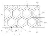
- the light-shielding layer 320 may have a print pattern.
- FIG. Fig. 3 is an enlarged view of a print pattern in the light-shielding layer at the interface between the display area S1 and the non-display area S2 of the polarizer of Fig. 4 is a cross-sectional view of a print pattern in the light-shielding layer at the interface between the display area S1 and the non-display area S2 of the polarizer of Fig.
- the light shielding layer 320 may include a plurality of printing patterns 323.
- the remaining area 324 of the light-shielding layer 320 excluding the printing area corresponds to an unprinted area.
- the print patterns 323 are formed to be spaced apart from each other.
- the print pattern 323 is composed of a first print layer 321 and a second print layer 322 formed on the first print layer 321.
- the second printed layer 322 may be formed directly on the first printed layer 321.
- the second print layer 322 may have a pattern shape different from that of the first print layer 321 or may be the same. For example, the area of the second printed layer 322 is smaller than the area of the first printed layer 321.
- the shortest distance DELTA L between a and b may be less than or equal to about 200 mu m, for example, from about 0.1 mu m to about 200 mu m, and alternatively, for example, from about 10 mu m to about 200 mu m. In the above range, the light shielding effect can be obtained and the uniformity between the display area and the non-display area is high, so that there is little difference in luminosity and RGB in the pixel may not be visually recognized.
- the present invention differs from the above-mentioned two printing patterns in that two printing patterns are stacked, but the light-shielding effect is simply increased, and the light-shielding effect is obtained by adjusting the shortest distance DELTA L, This is because the uniformity is high so that the difference in the sensibility is small and the RGB in the pixel is not visually recognized.
- the term "interface between the display area and the non-display area" refers to a surface of the first print layer formed in the non-display area, to which a plurality of one point of the first print layer closest to the non-
- the difference between the length of the maximum longitudinal axis 321L of the first printed layer 321 and the length of the maximum longitudinal axis 322L of the second printed layer 322 is about 200 ⁇ m or less, About 200 microns, and in another example about 10 microns to about 200 microns.
- the light shielding effect can be obtained and the uniformity between the display area and the non-display area is high, so that there is little difference in luminosity and RGB in the pixel may not be visually recognized.
- two print patterns are stacked in a multilayer structure as shown in FIG. 3 and FIG.
- the length of the longest axis 321L of the first printed layer 321 is about 50 ⁇ m to about 600 ⁇ m, for example, about 100 ⁇ m to about 500 ⁇ m, and the length of the longest axis 322L of the second printed layer 322 is From about 50 [mu] m to about 500 [mu] m, for example from about 50 [mu] m to about 350 [
- first print layer 321 and the second print layer 322 have different shapes from each other in the print pattern 323, the first print layer 321 is printed and then the second print layer 322 is printed It can not but be formed.
- the first printing layer and the second printing layer can be simultaneously formed as one metal mold, but the metal mold processing is not easy and the shape of the pattern is not well displayed.
- the print pattern must be printed in parallel, but when the second print layer 322 is formed on the first print layer 321, a curved surface is inevitable.
- the length difference ⁇ L between the long axis 321L of the first printed layer 321 and the long axis 322L of the second printed layer 322 is about 200 ⁇ m or less, for example, about 0.1 ⁇ m to about 200 ⁇ m, For another example from about 10 [mu] m to about 200 [mu] m.
- the first printed layer 321 may have a hexagonal shape
- the second printed layer 322 may have a rhombus shape.
- the present invention is not limited thereto.
- the first print layer may be an N-square (N is an integer of 3 to 10), a circle, an ellipse, an amorphous or the like such as an octagonal shape, 3 to 10), circular, elliptical, amorphous, and the like.
- the length of one side constituting the first print layer 321 may be the same or different, and may be about 10 ⁇ to about 400 ⁇ , for example, about 50 ⁇ to about 300 ⁇ .
- the lengths of one side constituting the second printed layer 322 may be the same or different, and may be about 10 ⁇ to about 400 ⁇ , for example, about 50 ⁇ to about 300 ⁇ .
- the length of one side constituting the first print layer 321 may be the same or different from the length of one side constituting the second print layer 322.
- the length of one side constituting the first printed layer 321 may be equal to the length of one side constituting the second printed layer 322.
- the first print layer 321 is regular hexagonal, the first print layer 321 is arranged in a honeycomb structure, and the second print layer 322 may be rhombus or square or amorphous.
- the area of the second printed layer 322 may be smaller than the area of the first printed layer 321.
- the second printed layer 322 can be formed on the first printed layer 321.
- the area ratio of the area of the first printed layer 321 to the area of the second printed layer 322 may be greater than about 1, for example greater than about 100% to about 3000%. In the above range, the uniformity between the display area and the non-display area is high, so that the difference in the sensibility is small and the RGB in the pixel may not be visually recognized.
- the intersection of the first print layer 321 and the second print layer 322 may be at least two, for example, three or more.
- the "intersection point" may mean the intersection of the rim of the first printed layer 321 and the rim of the second printed layer 322, as shown in Fig. In such a case, the uniformity between the display area and the non-display area is high, so that the difference in luminance is small and the RGB in the pixel may not be visually recognized.
- a point at which the first printed layer 321 contacts the interface between the display area S1 and the non-display area S2 is a, and the first printed layer 321 immediately adjacent to the first printed layer 321 is a display area S1) and the non-display area S2 is b, the distance between a and b is W.
- a vertex or inflection point closest to a in the first printing layer 321 is denoted by c and a closest vertex or inflection point from b in the first printing layer 321 is denoted by d
- the distance from the interface between the display area S1 and the non-display area S2 to the distance c and the distance from the interface between the display area S1 and the non-display area S2 to the distance d is H.
- H may be less than or equal to about 200 microns, such as from about 0.1 microns to about 200 microns, and alternatively from about 5 microns to about 200 microns. In the above range, the light shielding effect is obtained and the uniformity between the display area and the non-display area is high, so that there is little difference in viewing and RGB in the pixel may not be visually recognized.
- the print pattern may satisfy the relationship:
- W may be from about 10 ⁇ to about 500 ⁇ , for example from about 10 ⁇ to about 490 ⁇ . W > H.
- the first print layer is hexagonal, the first print layer is arranged in a honeycomb structure, and the second print layer may be rhombus, square, regular hexagon or amorphous.
- the print patterns 323 are formed to be spaced apart from each other.
- the spacing distance T between the print patterns 323 may be from about 1 [mu] m to about 50 [mu] m, for example from about 5 [mu] m to about 30 [mu] m. In the above range, the light shielding effect can be obtained, and the uniformity can be not affected.
- the light shielding layer 320 may be partially open between the polarizer 100 and the first polarizer protective film 200. That is, the light-shielding layer 320 may be in the form of a closed polygon, and may include some empty areas inside. Accordingly, the inside of the light shielding layer 320 described above may be defined as an empty space inside the light shielding layer 320 forming the closed polygon.
- the light shielding layer 320 may be disposed on at least a part or all of the outer edge on the horizontal section of the polarizer 100 and the first polarizer protective film 200. However, the present invention is not limited thereto.
- the thickness of each of the first print layer 321 and the second print layer 322 may be less than about 5 mu m, for example, about 0.1 mu m or more and less than about 5 mu m, May be the same or different. Within the above range, it can be contained in the adhesive layer, securing the light shielding property, and making the polarizing plate thinner.
- Figs. 3 and 4 show a case where the print pattern is formed as a two-layer print layer of the first print layer and the second print layer.
- the present invention is not limited thereto, and the print pattern may be formed as a single layer or a multilayer of two or more layers.
- FIGS. 3 and 4 show a case where the first print layer is formed directly on the first polarizer protective film.
- a polarizing plate in which another printing layer is further formed under the first printing layer, i.e., between the first polarizing protective film and the first printing layer, may be included in the scope of the present invention.
- the adhesive layer 310 may be interposed between the polarizer 100 and the first polarizer protective film 200 to adhere the polarizer 100 and the first polarizer protective film 200 to each other.
- the adhesive layer 310 is formed directly on the polarizer 100 and the first polarizer protective film 200, respectively.
- the adhesive layer 310 may be formed on at least one surface of each of the polarizer 100 and the first polarizer protective film 200. That is, the polarizer 100 and the first polarizer protective film 200 face each other, and they may have substantially the same area on a horizontal section.
- the adhesive layer 310 may be formed only on a part of the adhesive layer 310 and more specifically the polarizer 100 and the first polarizer protective film 200, And may be arranged in an island shape only in the center portion except for the rim.
- the adhesive layer 310 may be formed directly in contact with the light shielding layer 320 so that the light shielding layer 320 can be stably formed in the polarizing plate 10.
- the adhesive layer 310 allows the polarizer 100 and the first polarizer protective film 200 to adhere to each other or to bond the polarizer 100 and the first polarizer protective film 200 to each other.
- the photocurable adhesive is not particularly limited, but it may be an ultraviolet curable adhesive.
- the photocurable adhesive may include at least one of epoxy resin, monomer or oligomer, (meth) acrylate resin, monomer or oligomer.
- the photocurable adhesive may further comprise at least one of a photopolymerization radical initiator, a light-ion initiator.
- Detailed classes of epoxy-based, (meth) acrylate-based, photopolymerizable radical initiators, and light-ion initiators are known to those skilled in the art.
- the thickness of the adhesive layer 310 may be about 2 ⁇ to about 5 ⁇ .
- a gap between the polarizer 100 and the first polarizer protective film 200 by the light-shielding layer 320 of the present invention can be scattered, thereby improving the durability of the polarizer. That is, the deviation between the region where the light blocking layer 320 is present and the region where the light blocking layer 320 is not present between the polarizer 100 and the first polarizer protective film 200 can be minimized.
- the first polarizer protective film 200 may be formed on one side of the adhesive layer 310 to support the adhesive layer 310 and the polarizer 100.
- the first polarizer protective film 200 may be an optically transparent protective film.
- the first polarizer protective film may be made of at least one selected from the group consisting of a polyester including polyethylene terephthalate (PET), polybutylene terephthalate, polyethylene naphthalate, polybutylene naphthalate and the like, acrylic, cyclic olefin polymer (COP) Polyvinyl acetate, polyvinyl chloride (PVC), polynorbornene, polycarbonate (PC), polyamide, polyacetal, polyphenylene ether, polyphenylene sulfide, poly (ethylene terephthalate) Sulfone, polyether sulfone, polyarylate, and polyimide.
- PET polyethylene terephthalate
- PVC polyvinyl chloride
- PC polycarbonate
- PC polyamide
- the first polarizer protective film 200 may have a thickness of about 30 ⁇ to about 120 ⁇ , specifically about 20 ⁇ to about 80 ⁇ . And can be used in an optical display device in the above range.
- the first polarizer protective film 200 may be an isotropic film or a retardation film.
- the retardation film may include a film having an in-plane retardation Re at a wavelength of 550 nm of greater than about 5 nm, such as from about 10 nm to about 15,000 nm.
- the second polarizer protective film 400 may have the same or different material, thickness, and phase difference as the first polarizer protective film 200 described above.
- the polarizer 100 is formed on the lower surface of the adhesive layer 310 to polarize the incident light.
- Polarizer 100 may comprise a polarizer.
- the polarizer may comprise conventional polarizers known to those skilled in the art.
- the polarizer may include a polyvinyl alcohol polarizer produced by uniaxially stretching a polyvinyl alcohol film, or a polyene polarizer produced by dehydrating a polyvinyl alcohol film.
- the polarizer 100 may have a thickness of about 5 ⁇ ⁇ to about 40 ⁇ ⁇ . In the above range, it can be used in an optical display device.
- an optical display device including the above-described polarizing plate can be provided.
- the optical display device may include a liquid crystal display device, an organic light emitting diode display device, and the like.
- the polarizing plate of the present invention can be disposed on the viewer side polarizing plate of the liquid crystal display device.
- the present invention provides a polarizer protective film on which a light shielding layer is formed and a polarizing plate capable of preventing cracks from occurring in the light shielding layer even when UV light is applied when the polarizer is cured with an ultraviolet curable adhesive.
- TMP-DC-1 manufactured by Sumitomo Osaka Cement Co., Ltd.
- pigment solid 30% by weight was used as a pigment dispersion containing 30% by weight of the pigment (A)
- a pigment dispersion (Sakata Co., CI-M-050) containing carbon black (% by weight of silver and tin 7: 3) and (A-2) was mixed and used as shown in Table 1 below.
- the binder resin (B) an acrylic pressure-sensitive adhesive resin (WA-9263, manufactured by Uin Chemtech) was used.
- (D) (D1) a UV absorber, benzophenone-based LOWILITE 20 (2-hydroxy-4-methoxybenzophenone, MWCM) as a UV curing agent (C) Tinuvin 292 (HALS series, BASF) as the UV stabilizer, propylene glycol methyl ether acetate (E) as the solvent (D), (D2) Tinuvin 477 F) As the silane coupling agent, 765 W of Tego was used.
- C Tinuvin 292 (HALS series, BASF) as the UV stabilizer
- E propylene glycol methyl ether acetate
- D2 Tinuvin 477 F
- silane coupling agent 765 W of Tego was used.
- a composition for a light-shielding layer was prepared by controlling the contents of the pigment dispersion, the binder resin, the thermosetting initiator, the UV absorber, the UV stabilizer, the solvent and the silane coupling agent as shown in Table 1 below.
- the first printing layer was formed by coating the light-shielding layer composition of Production Example 1 with gravure coating on the edge of one side of the polyethylene terephthalate (PET) film.
- the printing roll is a first printing layer having a regular hexagonal shape and spaced apart from each other and having a honeycomb structure in a honeycomb shape.
- the first printed layer is a regular hexagon having a length of one side of 50 mu m.
- a second print layer was formed with another print roll.
- a second printed layer was formed from the composition for a light-shielding layer of Production Example 1.
- the printing roll is rhombic as the second printing layer, and the length of one side is 50 mu m.
- the second printing layer was formed on the first printing layer, and the long axes of the first printing layer and the second printing layer were parallel to each other.
- a light-shielding layer having the structure shown in Figs. 3 and 4 was formed.
- thermal curing through removal of the solvent at 85 ° C to 110 ° C for 2 minutes to form a light-shielding layer (thickness: 2 ⁇ m).
- the adhesive composition was applied to one side of the PET film on which the light-shielding layer was formed, an adhesive composition was applied to one surface of a cycloolefin polymer film (ZB12-052125, Zeon) as a second polarizer protective film, (Thickness: 4 ⁇ ⁇ ), a polarizer, an adhesive layer (thickness: 3 ⁇ ⁇ ) and a second polarizer protective film were successively formed on the surface of the PET film on which the light-shielding layer was formed, .
- the ultraviolet curing was carried out under the condition of metal halide lamp 400 mW / cm2 and 1000 mJ / cm2 in the condition of temperature 22 ⁇ 25 °C and humidity 20 ⁇ 60%.
- a polarizing plate was prepared in the same manner as in Example 1, except that the composition for a light-shielding layer in Table 2 was used instead of the composition for a light-shielding layer in Production Example 1 in the formation of the first printing layer and the second printing layer.
- a polarizing plate was produced in the same manner as in Example 1, except that the composition for a light-shielding layer of Production Example 5 was used instead of the composition for a light-shielding layer of Production Example 1 in the formation of the first printing layer and the second printing layer.
- Light shielding property The light shielding layer of the polarizing plate obtained in Examples and Comparative Examples was measured using an optical densitometer (TD-904: Greater Tag Macbeth) based on JIS K7651: 1988 using a UV filter.
- the evaluation in the light-shielding layer was determined by the absorbance value at a wavelength of 550 nm of a UV-visible spectrophotometer (JASC0-750). ? Has an absorbance value of 2.0 or more,? Is more than 1.5 and less than 2.0,? Is more than 1.0 and not more than 1.5, and X has a value of 1.0 or less. The higher the absorbance value, the higher the shading property.
- Reliability 1 A polarizing plate of Examples and Comparative Examples was cut into a length x width 300 mm x 150 mm to prepare a specimen.
- the specimen was put into Q-SUN Xe-B-1, a weather-resistance measuring apparatus, and sunlight was irradiated for 500 hours on the surface of the PET film on which the light-shielding layer was formed.
- the a * and b * values of the specimens were measured, and the areas where the light-shielding layer was formed were placed in a colorimeter (CM-3600d, Minolta Co.).
- the a * and b * values were measured before and after the solar irradiation.
- Reliability 2 Specimens were prepared by cutting the polarizing plates of Examples and Comparative Examples to a length of x 300 mm x 150 mm. The specimen was put into Q-SUN Xe-B-1, a weather-resistance measuring apparatus, and sunlight was irradiated for 500 hours on the surface of the PET film on which the light-shielding layer was formed. The irradiated specimens were measured, and the OD value of the portion where the light-shielding layer was formed was measured by X-Rite 300. The OD value was measured before and after the solar irradiation.
- the polarizing plate of the present invention was excellent in light shielding property and contained no UV absorber in the light shielding layer, so that no crack occurred even when the polarizer and the protective film were UV-cured with UV curable adhesive. Further, in the polarizing plate of the present invention, even after long-term UV irradiation, the rate of change of a * and b * of the polarizing plate before irradiation was low. In addition, the polarizing plate of the present invention has a low rate of change of the OD value before irradiation even after long-term UV irradiation, and thus the change in light blocking property can be minimized.
- Comparative Example 1 in which the UV absorber was not included in the light-shielding layer, cracks were generated when the polarizer and protective film were UV-cured with an ultraviolet curable adhesive, and thus could not be used as a polarizing plate.
- the amount of change in a *, b *, and OD value after irradiation for a long period of time after UV irradiation was larger than that in the Examples.
Abstract
La présente invention concerne une plaque polarisante et un dispositif d'affichage optique la comprenant. La plaque polarisante comprend une zone d'affichage et une zone de non-affichage encerclant la zone d'affichage. La plaque polarisante comprend un polariseur, une couche adhésive et un premier film de protection de polariseur, la couche adhésive et le premier film de protection de polariseur étant successivement stratifiés sur la surface supérieure du polariseur. La couche adhésive comprend une couche de blocage de lumière disposée en son sein et constitue au moins une partie de la zone de non-affichage. La couche de blocage de lumière est formée sur au moins une surface du premier film de protection de polariseur et comprend un agent absorbant les UV.
Applications Claiming Priority (2)
| Application Number | Priority Date | Filing Date | Title |
|---|---|---|---|
| KR10-2017-0183239 | 2017-12-28 | ||
| KR1020170183239A KR102126057B1 (ko) | 2017-12-28 | 2017-12-28 | 편광판 및 이를 포함하는 광학표시장치 |
Publications (1)
| Publication Number | Publication Date |
|---|---|
| WO2019132242A1 true WO2019132242A1 (fr) | 2019-07-04 |
Family
ID=67058840
Family Applications (1)
| Application Number | Title | Priority Date | Filing Date |
|---|---|---|---|
| PCT/KR2018/013910 WO2019132242A1 (fr) | 2017-12-28 | 2018-11-14 | Plaque polarisante et dispositif d'affichage optique la comprenant |
Country Status (4)
| Country | Link |
|---|---|
| US (1) | US20190204479A1 (fr) |
| KR (1) | KR102126057B1 (fr) |
| TW (1) | TWI697530B (fr) |
| WO (1) | WO2019132242A1 (fr) |
Families Citing this family (4)
| Publication number | Priority date | Publication date | Assignee | Title |
|---|---|---|---|---|
| KR102126054B1 (ko) * | 2017-12-21 | 2020-06-23 | 삼성에스디아이 주식회사 | 편광판 및 이를 포함하는 광학표시장치 |
| KR102126057B1 (ko) * | 2017-12-28 | 2020-06-23 | 삼성에스디아이 주식회사 | 편광판 및 이를 포함하는 광학표시장치 |
| JP6930017B2 (ja) * | 2020-01-14 | 2021-09-01 | 住友化学株式会社 | フレキシブル光学積層体および画像表示装置 |
| CN111983746A (zh) * | 2020-08-07 | 2020-11-24 | 深圳市华星光电半导体显示技术有限公司 | 一种偏光片和显示装置 |
Citations (5)
| Publication number | Priority date | Publication date | Assignee | Title |
|---|---|---|---|---|
| KR20140058995A (ko) * | 2012-11-07 | 2014-05-15 | 엘지디스플레이 주식회사 | 액정표시 장치 |
| KR20160110134A (ko) * | 2015-03-10 | 2016-09-21 | 스미또모 가가꾸 가부시키가이샤 | 프로텍트 필름 부착 편광판 및 액정 패널 |
| KR20170043450A (ko) * | 2015-10-13 | 2017-04-21 | 닛토덴코 가부시키가이샤 | 점착 시트, 점착제층을 갖는 편광판 및 화상 표시 장치 |
| KR20170073918A (ko) * | 2015-12-21 | 2017-06-29 | 삼성에스디아이 주식회사 | 편광판 및 이의 제조방법 및 이를 포함하는 표시 장치 |
| WO2017126883A1 (fr) * | 2016-01-19 | 2017-07-27 | 삼성에스디아이 주식회사 | Plaque polarisante et dispositif d'affichage optique la comprenant |
Family Cites Families (10)
| Publication number | Priority date | Publication date | Assignee | Title |
|---|---|---|---|---|
| TW383324B (en) * | 1994-10-13 | 2000-03-01 | Ciba Sc Holding Ag | UV absorbants and the use |
| ES2199696B1 (es) * | 2000-05-31 | 2005-03-01 | Ciba Specialty Chemicals Holding Inc. | Mezclas de estabilizantes. |
| JP2003043462A (ja) * | 2001-07-30 | 2003-02-13 | Nec Corp | 液晶表示装置及びその製造方法 |
| CA2458492A1 (fr) * | 2001-08-27 | 2003-03-06 | Hagihara Industries Inc. | Feuille pare-lumiere |
| JP2013254116A (ja) | 2012-06-07 | 2013-12-19 | Dainippon Printing Co Ltd | 光学積層体、及びこれを用いた偏光板 |
| JP2014213596A (ja) * | 2013-04-30 | 2014-11-17 | 新日鉄住金化学株式会社 | 樹脂積層体 |
| KR20160097429A (ko) * | 2015-02-06 | 2016-08-18 | 삼성디스플레이 주식회사 | 표시 장치 |
| WO2017051844A1 (fr) | 2015-09-25 | 2017-03-30 | 富士フイルム株式会社 | Corps stratifié optique, plaque de polarisation, procédé de fabrication de plaque de polarisation, et dispositif d'affichage d'image |
| KR101871565B1 (ko) * | 2016-01-19 | 2018-06-27 | 삼성에스디아이 주식회사 | 편광판 및 이를 포함하는 표시 장치 |
| KR102126057B1 (ko) * | 2017-12-28 | 2020-06-23 | 삼성에스디아이 주식회사 | 편광판 및 이를 포함하는 광학표시장치 |
-
2017
- 2017-12-28 KR KR1020170183239A patent/KR102126057B1/ko active IP Right Grant
-
2018
- 2018-11-14 WO PCT/KR2018/013910 patent/WO2019132242A1/fr active Application Filing
- 2018-11-29 US US16/205,144 patent/US20190204479A1/en active Pending
- 2018-12-04 TW TW107143498A patent/TWI697530B/zh active
Patent Citations (5)
| Publication number | Priority date | Publication date | Assignee | Title |
|---|---|---|---|---|
| KR20140058995A (ko) * | 2012-11-07 | 2014-05-15 | 엘지디스플레이 주식회사 | 액정표시 장치 |
| KR20160110134A (ko) * | 2015-03-10 | 2016-09-21 | 스미또모 가가꾸 가부시키가이샤 | 프로텍트 필름 부착 편광판 및 액정 패널 |
| KR20170043450A (ko) * | 2015-10-13 | 2017-04-21 | 닛토덴코 가부시키가이샤 | 점착 시트, 점착제층을 갖는 편광판 및 화상 표시 장치 |
| KR20170073918A (ko) * | 2015-12-21 | 2017-06-29 | 삼성에스디아이 주식회사 | 편광판 및 이의 제조방법 및 이를 포함하는 표시 장치 |
| WO2017126883A1 (fr) * | 2016-01-19 | 2017-07-27 | 삼성에스디아이 주식회사 | Plaque polarisante et dispositif d'affichage optique la comprenant |
Also Published As
| Publication number | Publication date |
|---|---|
| KR20190080661A (ko) | 2019-07-08 |
| TW201930503A (zh) | 2019-08-01 |
| KR102126057B1 (ko) | 2020-06-23 |
| TWI697530B (zh) | 2020-07-01 |
| US20190204479A1 (en) | 2019-07-04 |
Similar Documents
| Publication | Publication Date | Title |
|---|---|---|
| WO2019132242A1 (fr) | Plaque polarisante et dispositif d'affichage optique la comprenant | |
| WO2016175580A1 (fr) | Film optique d'amélioration de rapport de contraste, plaque de polarisation le comprenant et dispositif d'affichage à cristaux liquides le comprenant | |
| WO2010021505A2 (fr) | Agent adhésif | |
| WO2013028047A2 (fr) | Adhésif | |
| WO2016111466A1 (fr) | Feuille optique et afficheur optique la comprenant | |
| WO2011105875A2 (fr) | Plaque de polarisation | |
| WO2018164348A1 (fr) | Polariseur et dispositif d'affichage optique comprenant celui-ci | |
| WO2018221872A1 (fr) | Plaque de polarisation, et dispositif d'affichage à cristaux liquides comprenant cette plaque | |
| WO2019031786A1 (fr) | Élément optique, élément de polarisation et dispositif d'affichage | |
| WO2015008925A1 (fr) | Film polarisant et appareil d'affichage d'images le comprenant | |
| WO2019083160A1 (fr) | Film à différence de phase de cristaux liquides, plaque de polarisation pour un dispositif d'affichage électroluminescent comprenant ce dernier et dispositif d'affichage électroluminescent comprenant ce dernier | |
| WO2017126883A1 (fr) | Plaque polarisante et dispositif d'affichage optique la comprenant | |
| WO2018155792A1 (fr) | Film optique améliorant le rapport de contraste, plaque de polarisation le comprenant, et dispositif d'affichage à cristaux liquides le comprenant | |
| WO2017048079A1 (fr) | Film protecteur de polariseur, plaque polarisante comprenant celui-ci, et dispositif d'affichage à cristaux liquides comprenant la plaque polarisante | |
| WO2017039209A1 (fr) | Substrat de fenêtre de couverture et dispositif d'affichage d'image comprenant celui-ci | |
| WO2019235832A1 (fr) | Composition adhésive | |
| WO2018043851A1 (fr) | Plaque polarisante et dispositif d'affichage optique la comprenant | |
| WO2019198893A1 (fr) | Unité de rétroéclairage, dispositif d'affichage comprenant l'unité de rétroéclairage et procédé de fabrication du dispositif d'affichage | |
| WO2020080757A1 (fr) | Plaque polarisante, panneau à cristaux liquides et dispositif d'affichage | |
| WO2016104976A1 (fr) | Feuille optique, et plaque de polarisation et afficheur à cristaux liquides comportant cette feuille optique | |
| WO2020071646A1 (fr) | Plaque polarisante et dispositif d'affichage optique la comprenant | |
| WO2020153640A1 (fr) | Plaque de polarisation et dispositif d'affichage optique la comprenant | |
| WO2012002706A2 (fr) | Film protecteur | |
| EP3625596A1 (fr) | Élément optique, élément de polarisation et dispositif d'affichage | |
| WO2021177648A1 (fr) | Film de fenêtre souple et dispositif d'affichage le comprenant |
Legal Events
| Date | Code | Title | Description |
|---|---|---|---|
| 121 | Ep: the epo has been informed by wipo that ep was designated in this application |
Ref document number: 18897330 Country of ref document: EP Kind code of ref document: A1 |
|
| NENP | Non-entry into the national phase |
Ref country code: DE |
|
| 122 | Ep: pct application non-entry in european phase |
Ref document number: 18897330 Country of ref document: EP Kind code of ref document: A1 |