WO2019130608A1 - 高調波処理回路及び増幅回路 - Google Patents
高調波処理回路及び増幅回路 Download PDFInfo
- Publication number
- WO2019130608A1 WO2019130608A1 PCT/JP2018/012041 JP2018012041W WO2019130608A1 WO 2019130608 A1 WO2019130608 A1 WO 2019130608A1 JP 2018012041 W JP2018012041 W JP 2018012041W WO 2019130608 A1 WO2019130608 A1 WO 2019130608A1
- Authority
- WO
- WIPO (PCT)
- Prior art keywords
- amplifier
- circuit
- harmonic processing
- processing circuit
- setting unit
- Prior art date
- Legal status (The legal status is an assumption and is not a legal conclusion. Google has not performed a legal analysis and makes no representation as to the accuracy of the status listed.)
- Ceased
Links
Images



Classifications
-
- H—ELECTRICITY
- H03—ELECTRONIC CIRCUITRY
- H03F—AMPLIFIERS
- H03F1/00—Details of amplifiers with only discharge tubes, only semiconductor devices or only unspecified devices as amplifying elements
- H03F1/56—Modifications of input or output impedances, not otherwise provided for
- H03F1/565—Modifications of input or output impedances, not otherwise provided for using inductive elements
-
- H—ELECTRICITY
- H01—ELECTRIC ELEMENTS
- H01P—WAVEGUIDES; RESONATORS, LINES, OR OTHER DEVICES OF THE WAVEGUIDE TYPE
- H01P1/00—Auxiliary devices
- H01P1/20—Frequency-selective devices, e.g. filters
- H01P1/212—Frequency-selective devices, e.g. filters suppressing or attenuating harmonic frequencies
-
- H—ELECTRICITY
- H03—ELECTRONIC CIRCUITRY
- H03F—AMPLIFIERS
- H03F1/00—Details of amplifiers with only discharge tubes, only semiconductor devices or only unspecified devices as amplifying elements
- H03F1/02—Modifications of amplifiers to raise the efficiency, e.g. gliding Class A stages, use of an auxiliary oscillation
- H03F1/0205—Modifications of amplifiers to raise the efficiency, e.g. gliding Class A stages, use of an auxiliary oscillation in transistor amplifiers
- H03F1/0288—Modifications of amplifiers to raise the efficiency, e.g. gliding Class A stages, use of an auxiliary oscillation in transistor amplifiers using a main and one or several auxiliary peaking amplifiers whereby the load is connected to the main amplifier using an impedance inverter, e.g. Doherty amplifiers
-
- H—ELECTRICITY
- H03—ELECTRONIC CIRCUITRY
- H03F—AMPLIFIERS
- H03F3/00—Amplifiers with only discharge tubes or only semiconductor devices as amplifying elements
- H03F3/04—Amplifiers with only discharge tubes or only semiconductor devices as amplifying elements with semiconductor devices only
-
- H—ELECTRICITY
- H03—ELECTRONIC CIRCUITRY
- H03F—AMPLIFIERS
- H03F3/00—Amplifiers with only discharge tubes or only semiconductor devices as amplifying elements
- H03F3/189—High-frequency amplifiers, e.g. radio frequency amplifiers
- H03F3/19—High-frequency amplifiers, e.g. radio frequency amplifiers with semiconductor devices only
- H03F3/195—High-frequency amplifiers, e.g. radio frequency amplifiers with semiconductor devices only in integrated circuits
-
- H—ELECTRICITY
- H03—ELECTRONIC CIRCUITRY
- H03F—AMPLIFIERS
- H03F3/00—Amplifiers with only discharge tubes or only semiconductor devices as amplifying elements
- H03F3/20—Power amplifiers, e.g. Class B amplifiers, Class C amplifiers
- H03F3/24—Power amplifiers, e.g. Class B amplifiers, Class C amplifiers of transmitter output stages
- H03F3/245—Power amplifiers, e.g. Class B amplifiers, Class C amplifiers of transmitter output stages with semiconductor devices only
-
- H—ELECTRICITY
- H03—ELECTRONIC CIRCUITRY
- H03F—AMPLIFIERS
- H03F2200/00—Indexing scheme relating to amplifiers
- H03F2200/222—A circuit being added at the input of an amplifier to adapt the input impedance of the amplifier
-
- H—ELECTRICITY
- H03—ELECTRONIC CIRCUITRY
- H03F—AMPLIFIERS
- H03F2200/00—Indexing scheme relating to amplifiers
- H03F2200/451—Indexing scheme relating to amplifiers the amplifier being a radio frequency amplifier
Definitions
- the present invention relates to a harmonic processing circuit and an amplifier circuit.
- This application claims priority based on Japanese Patent Application No. 2017-254355 filed on Dec. 28, 2017, and incorporates all the contents described in the aforementioned Japanese application.
- harmonic processing performed to improve the power efficiency of an amplifier it is generally performed to provide an open stub on a signal line for adjusting the impedance to the harmonic to an appropriate value.
- Patent Document 1 For example, refer to Patent Document 1).
- a harmonic processing circuit includes a branch line branched from a signal line through which a signal input to and output from an amplifier is transmitted, and a setting unit connected to the branch line and setting an impedance to a harmonic of the signal. And at least a part of the setting unit is configured by a lumped constant circuit.
- FIG. 1 is a block diagram showing the configuration of a Doherty amplifier circuit according to an embodiment.
- FIG. 2 is a plan view of the Doherty amplifier circuit.
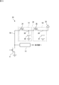
- FIG. 3 is a block diagram showing the configuration of the first harmonic processing circuit.
- FIG. 4 is a Smith chart showing the load impedance with respect to the frequency change of the signal in the amplifier circuit according to the embodiment.
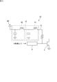
- FIG. 5 is a block diagram showing the configuration of a harmonic processing circuit provided on the gate terminal side.
- the size of the open stub as a circuit for performing the harmonic processing is determined according to the wavelength of the signal to be processed. That is, since the open stub needs to have a certain size, there is a problem that miniaturization is difficult.
- This indication is made in view of such a situation, and aims at offer of a harmonic processing circuit and amplifier which can be miniaturized.
- a harmonic processing circuit is connected to a branch line branched from a signal line through which a signal input to or output from an amplifier is transmitted, and the branch line to set an impedance to harmonics of the signal And at least a part of the setting unit is configured of a lumped constant circuit.
- the harmonic processing circuit having the above configuration, at least a part of the setting unit for setting the impedance to the harmonic is constituted by the lumped constant circuit. Therefore, the setting unit is compared to the case where harmonic processing is performed using the open stub. Can be reduced, and the overall circuit can be miniaturized.
- the branch line is preferably a feed line of the amplifier.
- the setting unit can be provided without adding a new line.
- the setting unit is set so that the branch line is open to the fundamental wave of the signal. In this case, it is possible to suppress the influence of the setting unit on the fundamental wave.
- the amplifier is housed in one package together with the other amplifier.
- the signal line connected to the amplifier and the signal lines of other amplifiers are arranged side by side, the space around the signal line is limited.
- the harmonic processing circuit can achieve miniaturization of the entire circuit, even if the space around the signal line is limited, it can be appropriately disposed.
- the setting unit includes a plurality of capacitive elements connected in parallel, and among the plurality of capacitive elements, at a position adjacent to a voltage source that applies a voltage to the feed line.
- the connected capacitive element is set to a capacitance that is shorted to the fundamental wave of the signal. In this case, the high frequency signal can be prevented from leaking to the voltage source side of the feed line.
- the setting unit is between the first inductance element connected to the branch line, the first inductance element, and a voltage source that applies a voltage to the feed line.
- a second capacitive element connected to one end, a first capacitive element connected at one end to the connection point between the first inductive element and the second inductive element, one end at the second inductive element, and And a second capacitive element connected to a connection point between the voltage source and the second capacitive element, wherein an inductance of the second inductance element is set to a value larger than an inductance of the first inductive element.
- the capacitance of the capacitor is set to a value larger than the capacitance of the first capacitive element. In this case, the value of each element can be set appropriately.
- an amplifier circuit which is another embodiment includes an amplifier, a signal line through which a signal input to and output from the amplifier is transmitted, and the harmonic processing circuit described in the above (1) to (6) And have.
- FIG. 1 is a block diagram showing the configuration of a Doherty amplifier circuit according to an embodiment.
- the Doherty amplifier circuit 1 is mounted on a wireless communication apparatus such as a base station apparatus in a mobile communication system, and amplifies a transmission signal (RF signal) of a radio frequency.
- the Doherty amplifier circuit 1 amplifies an RF signal (input signal) applied to the input terminal 2 and outputs the amplified signal from an output terminal 3.
- the Doherty amplifier circuit 1 combines the outputs of the carrier amplifier 4, the peak amplifier 5 provided in parallel to the carrier amplifier 4, the distributor 6, the carrier amplifier 4 and the peak amplifier 5.
- a combiner 7, a carrier side input matching circuit 8, a peak side input matching circuit 9, a carrier side output matching circuit 10, and a peak side output matching circuit 11 are provided.
- the distributor 6 is connected to the subsequent stage of the input terminal 2 and distributes the RF signal supplied from the input terminal 2 to the carrier amplifier 4 and the peak amplifier 5.
- the output of the distributor 6 is applied to the carrier amplifier 4 via the carrier-side input matching circuit 8 and to the peak amplifier 5 via the peak-side input matching circuit 9.
- the carrier side input matching circuit 8 performs impedance matching for the fundamental wave between the distributor 6 side and the carrier amplifier 4 side.
- the peak side input matching circuit 9 performs impedance matching on the fundamental wave between the distributor 6 side and the peak amplifier 5 side.
- Carrier amplifier 4 is an amplifier for always amplifying an input signal supplied.
- the peak amplifier 5 is an amplifier for amplifying the input signal when the power of the input signal exceeds a predetermined level.
- the carrier amplifier 4 and the peak amplifier 5 are, for example, high electron mobility transistors (HEMTs) using gallium nitride (GaN).
- HEMTs high electron mobility transistors
- GaN gallium nitride
- the carrier amplifier 4 and the peak amplifier 5 are mounted on one integrated circuit and accommodated in one package 20.
- the output of the carrier amplifier 4 is provided to the combiner 7 via the carrier side output matching circuit 10. Further, the output of the peak amplifier 5 is given to the combiner 7 via the peak side output matching circuit 11.
- the carrier side output matching circuit 10 performs impedance matching on the fundamental wave between the carrier amplifier 4 side and the combiner 7 side.
- the peak side output matching circuit 11 performs impedance matching on the fundamental wave between the peak amplifier 5 side and the combiner 7 side.
- the combiner 7 combines the output of the carrier amplifier 4 and the output of the peak amplifier 5.
- the combiner 7 applies the combined output to the output terminal 3 as an output signal.
- the output terminal 3 outputs the output signal supplied from the combiner 7.
- FIG. 2 is a plan view of the Doherty amplifier circuit 1. As shown in FIG. 2, the package 20 in which the amplifiers 4 and 5 are accommodated, the input / output terminals 2 and 3, the distributor 6, the combiner 7, and the matching circuits 8, 9, 10 and 11 are provided on the circuit board 25. Has been implemented.
- a first drain power supply 30, a second drain power supply 40, a first gate power supply 60, and a second gate power supply 70 provided outside the circuit board 25 are connected to the Doherty amplifier circuit 1.
- the first drain power supply 30 is a power supply for supplying a drain voltage applied to the carrier amplifier 4, and is connected to the drain terminal of the carrier amplifier 4 via the first feed line 31.
- the second drain power supply 40 is a power supply for supplying a drain voltage applied to the peak amplifier 5, and is connected to the drain terminal of the peak amplifier 5 via the second feed line 41.
- the first gate power supply 60 is a power supply for supplying a gate voltage applied to the carrier amplifier 4, and is connected to the gate terminal of the carrier amplifier 4 via the third feed line 61.
- the second gate power supply 70 is a power supply for supplying a gate voltage applied to the peak amplifier 5, and is connected to the gate terminal of the peak amplifier 5 via the fourth feed line 71.
- a first setting unit 32 is connected to the first feed line 31.
- the first setting unit 32 performs harmonic processing of the output of the carrier amplifier 4 supplied to the carrier side output matching circuit 10.
- a second setting unit 42 is connected to the second feed line 41 to perform harmonic processing of the output of the peak amplifier 5 supplied to the peak side output matching circuit 11.
- the first setting unit 32 and the second setting unit 42 perform processing (harmonic processing) to adjust the impedance to the harmonic of the signal in the carrier side output matching circuit 10 and the peak side output matching circuit 11 to an appropriate value.
- the first setting unit 32 connected to the first feed line 31 and the first feed line 31 constitutes a first harmonic processing circuit 33.
- the second setting unit 42 connected to the second feed line 41 and the second feed line 41 constitutes a second harmonic processing circuit 43.
- FIG. 3 is a block diagram showing the configuration of the first harmonic processing circuit 33.
- the second harmonic processing circuit 43 is also similar to the configuration of the first harmonic processing circuit 33. Therefore, only the first harmonic processing circuit 33 will be described here.
- the first harmonic processing circuit 33 is configured to include a first inductance element 34, a second inductance element 35, a first capacitance element 36, and a second capacitance element 37. . These elements 34, 35, 36, 37 are lumped elements, and the first harmonic processing circuit 33 is configured as a lumped circuit.
- the first inductance element 34 and the second inductance element 35 are connected to the first feed line 31.
- One end of the first capacitive element 36 is connected to a connection point 38 between the first inductance element 34 and the second inductance element 35, and the other end is grounded.
- One end of the second capacitive element 37 is connected to a connection point 39 between the second inductance element 35 and the first drain power supply 30, and the other end is grounded.
- the first capacitive element 36 and the second capacitive element 37 are connected in parallel.
- the first harmonic processing circuit 33 includes the first LC circuit 51 including the first inductance element 34 and the first capacitance element 36, the second inductance element 35, and the second capacitance element 37. And a second LC circuit 52. That is, the first harmonic processing circuit 33 is configured by connecting LC circuits in two stages.
- the first setting unit 32 (second setting unit 42) for setting the impedance to the harmonics is configured by a lumped constant circuit, for example.
- the first setting unit 32 (second setting unit 42) can be made smaller as compared to the case where harmonic processing is performed using an open stub, and the overall circuit can be miniaturized. it can.
- the first setting unit 32 (the second setting unit 42) in the first feed line 31 (the second feed line 41)
- the first feed line 31 (the second feed line 41) can be obtained.
- the first setting unit 32 (second setting unit 42) can be provided without adding a new line. .
- the harmonic processing circuit is provided in the Doherty amplifier circuit 1 having the amplifiers 4 and 5, the enlargement of the Doherty amplifier circuit 1 can be suppressed by the installation of the harmonic processing circuit.
- the first setting unit 32 (second setting unit 42) is a signal in which the first feed line 31 (second feed line 41) is the carrier-side output matching circuit 10 (peak-side output matching circuit 11). It is set to be open to the fundamental wave of. In this case, the influence of the first setting unit 32 (second setting unit 42) on the fundamental wave can be suppressed.
- the first setting unit 32 includes a plurality of (two) capacitive elements 36 and 37 connected in parallel, and among the capacitive elements 36 and 37, the first setting unit 32 is adjacent to the first drain power supply 30.
- the second capacitive element 37 connected to the position is set to a capacitance that is shorted to the fundamental wave of the signal in the carrier side output matching circuit 10. This can prevent the high frequency signal from leaking to the voltage source side of the feed line.
- the inductance of the second inductance element 35 is set to a value larger than the inductance of the first inductance element 34, and the capacitance of the second capacitive element 37 is larger than the capacitance of the first capacitive element 36. It is set to a value. By setting so as to satisfy such a relationship, the value of each element can be appropriately set while the capacitance of the second capacitive element 37 and other conditions are satisfied.
- the capacitance of the first capacitive element 36 may be set to an extremely small value. Therefore, the first capacitive element 36 may not be connected between the first inductance element 34 and the second inductance element 35 in some cases.
- the carrier side output matching circuit 10 and the peak side output matching circuit 11 are arranged side by side. (FIG. 2)
- the space around the matching circuits 10, 11 is limited.
- the harmonic processing circuit 33 of this embodiment can achieve miniaturization of the entire circuit, even if the space around the matching circuits 10 and 11 is limited, it is appropriate. It can be arranged.
- the harmonic processing circuit of the embodiment has a configuration similar to that of the first harmonic processing circuit 33 shown in FIG. 3 and includes the first inductance element 34, the second inductance element 35, the first capacitance element 36, the first The configuration includes two capacitive elements 37, and two stages of LC circuits are connected.
- the harmonic processing circuit was set to perform harmonic processing on the second harmonic of a frequency of 2.6 GHz. More specifically, the value of each element was set so that the phase of the second harmonic (frequency 5.2 GHz) would be about 85 degrees.
- the second capacitive element is set to a capacitance that causes a short circuit with respect to the fundamental wave.
- First inductance element 2.2 nH Second inductance element: 3.3 nH First capacitive element: 0.5 pF Second capacitive element: 10 pF
- FIG. 4 is a Smith chart showing the load impedance with respect to the frequency change of the signal in the amplifier circuit according to the embodiment.
- a marker m1 indicates a load impedance at a frequency of 2.6 GHz.
- a marker m3 indicates a load impedance at a frequency of 5.2 GHz.
- the load impedance of the marker m1 is 0.978 in magnitude and 2.433 in phase, and is almost open.
- the load impedance of the marker m3 has a magnitude of 0.943 and a phase of 84.285, and it can be confirmed that harmonic processing can be performed almost as intended.
- the first setting unit 32 in which the LC circuits are connected in two stages is illustrated, but the LC circuits may be connected in multiple stages such as three or four stages.
- the LC circuits may be connected in multiple stages such as three or four stages.
- harmonic processing up to the second harmonic is possible
- harmonic processing up to the third harmonic is possible It becomes.
- the number of connections of the LC circuit is set according to the order of harmonics to be processed.
- the first setting unit 32 in which each of the elements 34, 35, 36, and 37 is formed of a lumped element is exemplified.
- the first inductance element 34 and the second inductance element are transmission lines. It may be used in combination or as a transmission line.
- the first inductance element 34 and the second inductance element 35 are configured as distributed constant elements
- the first capacitance element 36 and the second capacitance element 37 are configured by lumped constant elements. Therefore, in this case, at least a part of the first setting unit 32 is configured by a lumped constant circuit.
- the first harmonics processing circuit 33 is connected to the first feed line 31 connected to the drain terminal of the carrier amplifier 4 and the second feed line 41 connected to the drain terminal of the peak amplifier 5;
- the setting unit 62 is provided in the third feed line 61 for supplying the gate voltage from the first gate power source 60.
- the harmonic processing circuit 63 may be provided.
- the setting unit 62 has the same configuration as the first setting unit 32 described in the above embodiment, and is configured by connecting the LC circuits 64 and 65 in two stages. The same applies to the second gate power supply 70 side, and the fourth feed line 71 may be provided with a harmonic processing circuit.
- the setting unit 62 can be made smaller by configuring the setting unit 62 for setting the impedance on the signal source side of the carrier amplifier 4 and the peak amplifier 5 with a lumped constant circuit.
- the overall size can be reduced, and further, the size of the entire Doherty amplifier circuit 1 can be reduced.
Landscapes
- Engineering & Computer Science (AREA)
- Power Engineering (AREA)
- Microelectronics & Electronic Packaging (AREA)
- Amplifiers (AREA)
Abstract
高調波処理回路(33)は、増幅器(4)に入出力される信号が伝送される信号線路から分岐した第1給電線路(31)と、第1給電線路(31)に接続され、前記信号の高調波に対するインピーダンスを設定する第1設定部(32)と、を備え、第1設定部(32)の少なくとも一部が集中定数回路で構成されている。
Description
本発明は、高調波処理回路及び増幅回路に関する。
本出願は、2017年12月28日出願の日本出願第2017-254355号に基づく優先権を主張し、前記日本出願に記載された全ての記載内容を援用するものである。
本出願は、2017年12月28日出願の日本出願第2017-254355号に基づく優先権を主張し、前記日本出願に記載された全ての記載内容を援用するものである。
従来から、増幅器の電力効率を向上させるために行われる高調波処理としては、高調波に対するインピーダンスを適切な値に調整するためのオープンスタブを信号線路に設けることが一般的に行われている(例えば、特許文献1参照)。
一実施形態である高調波処理回路は、増幅器に入出力される信号が伝送される信号線路から分岐した分岐線路と、前記分岐線路に接続され、前記信号の高調波に対するインピーダンスを設定する設定部と、を備え、前記設定部の少なくとも一部が集中定数回路で構成されている。
[本開示が解決しようとする課題]
高調波処理を行うための回路としての上記オープンスタブは、処理対象となる信号の波長に応じてその大きさが定まる。つまり、上記オープンスタブは、一定の大きさを確保する必要あるため、小型化が困難であるという問題を有している。
高調波処理を行うための回路としての上記オープンスタブは、処理対象となる信号の波長に応じてその大きさが定まる。つまり、上記オープンスタブは、一定の大きさを確保する必要あるため、小型化が困難であるという問題を有している。
本開示はこのような事情に鑑みてなされたものであり、小型化が可能な高調波処理回路及び増幅回路の提供を目的とする。
[本開示の効果]
本開示によれば、高調波処理回路の小型化が可能となる。
本開示によれば、高調波処理回路の小型化が可能となる。
最初に実施形態の内容を列記して説明する。
[実施形態の概要]
(1) 一実施形態である高調波処理回路は、増幅器に入出力される信号が伝送される信号線路から分岐した分岐線路と、前記分岐線路に接続され、前記信号の高調波に対するインピーダンスを設定する設定部と、を備え、前記設定部の少なくとも一部が集中定数回路で構成されている。
[実施形態の概要]
(1) 一実施形態である高調波処理回路は、増幅器に入出力される信号が伝送される信号線路から分岐した分岐線路と、前記分岐線路に接続され、前記信号の高調波に対するインピーダンスを設定する設定部と、を備え、前記設定部の少なくとも一部が集中定数回路で構成されている。
上記構成の高調波処理回路によれば、高調波に対するインピーダンスを設定する設定部の少なくとも一部を集中定数回路で構成したので、オープンスタブを用いて高調波処理を行う場合と比較して設定部を小さくすることができ、回路全体の小型化を図ることができる。
(2)上記高調波処理回路において、前記分岐線路は、前記増幅器の給電線路であることが好ましい。
この場合、既存の給電線路を分岐線路として用いることで、新たな線路を追加することなく設定部を設けることができる。
これにより、増幅器を有する回路に高調波処理回路を設けたとしても、高調波処理回路の設置によって前記回路が大型化するのを抑制することができる。
この場合、既存の給電線路を分岐線路として用いることで、新たな線路を追加することなく設定部を設けることができる。
これにより、増幅器を有する回路に高調波処理回路を設けたとしても、高調波処理回路の設置によって前記回路が大型化するのを抑制することができる。
(3)また、上記高調波処理回路において、前記設定部は、前記分岐線路が前記信号の基本波に対してオープンとなるように設定されていることが好ましい。
この場合、設定部が基本波に対して与える影響を抑制することができる。
この場合、設定部が基本波に対して与える影響を抑制することができる。
(4)また、上記高調波処理回路において、前記増幅器は、他の増幅器とともに一つのパッケージに収容されていることが好ましい。
この場合、増幅器に接続される信号線路と、他の増幅器の信号線路とが隣り合って並ぶため、信号線路周囲のスペースが制限される。しかし、この場合であっても、高調波処理回路は、回路全体の小型化を図ることができるので、信号線路周囲のスペースが制限されたとしても適切に配置することができる。
この場合、増幅器に接続される信号線路と、他の増幅器の信号線路とが隣り合って並ぶため、信号線路周囲のスペースが制限される。しかし、この場合であっても、高調波処理回路は、回路全体の小型化を図ることができるので、信号線路周囲のスペースが制限されたとしても適切に配置することができる。
(5)上記高調波処理回路において、前記設定部は、並列に接続された複数の容量素子を含み、前記複数の容量素子のうち、前記給電線路に電圧を印加する電圧源に隣接する位置に接続されている容量素子は、前記信号の基本波に対してショートとなる容量に設定されている。
この場合、給電線路の電圧源側へ高周波信号が漏洩するのを防止することができる。
この場合、給電線路の電圧源側へ高周波信号が漏洩するのを防止することができる。
(6)また、上記高調波処理回路において、前記設定部は、前記分岐線路に接続された第1インダクタンス素子と、前記第1インダクタンス素子と、前記給電線路に電圧を印加する電圧源との間に接続された第2インダクタンス素子と、一端が前記第1インダクタンス素子と、前記第2インダクタンス素子との間の接続点に接続された第1容量素子と、一端が前記第2インダクタンス素子と、前記電圧源との間の接続点に接続された第2容量素子と、を含み、前記第2インダクタンス素子のインダクタンスは、前記第1インダクタンス素子のインダクタンスよりも大きい値に設定され、前記第2容量素子の容量は、前記第1容量素子の容量よりも大きい値に設定されていることが好ましい。
この場合、各素子の値を適切に設定することができる。
この場合、各素子の値を適切に設定することができる。
(7)また、他の実施形態である増幅回路は、増幅器と、前記増幅器に入出力される信号が伝送される信号線路と、上記(1)から(6)に記載された高調波処理回路と、を備えている。
[実施形態の詳細]
以下、好ましい実施形態について図面を参照しつつ説明する。
なお、以下に記載する各実施形態の少なくとも一部を任意に組み合わせてもよい。
以下、好ましい実施形態について図面を参照しつつ説明する。
なお、以下に記載する各実施形態の少なくとも一部を任意に組み合わせてもよい。
〔ドハティ増幅回路の構成〕
図1は、一実施形態に係るドハティ増幅回路の構成を示すブロック図である。
このドハティ増幅回路1は、移動体通信システムにおける基地局装置などの無線通信装置に搭載され、無線周波数の送信信号(RF信号)の増幅を行う。
ドハティ増幅回路1は、入力端子2に与えられるRF信号(入力信号)を増幅し、出力端子3から出力する。
図1は、一実施形態に係るドハティ増幅回路の構成を示すブロック図である。
このドハティ増幅回路1は、移動体通信システムにおける基地局装置などの無線通信装置に搭載され、無線周波数の送信信号(RF信号)の増幅を行う。
ドハティ増幅回路1は、入力端子2に与えられるRF信号(入力信号)を増幅し、出力端子3から出力する。
図1に示すように、ドハティ増幅回路1は、キャリア増幅器4と、キャリア増幅器4に並列に設けられたピーク増幅器5と、分配器6と、キャリア増幅器4及びピーク増幅器5それぞれの出力を合成する合成器7と、キャリア側入力整合回路8と、ピーク側入力整合回路9と、キャリア側出力整合回路10と、ピーク側出力整合回路11とを備えている。
分配器6は、入力端子2の後段に接続され、入力端子2から与えられるRF信号をキャリア増幅器4及びピーク増幅器5へ分配する。
分配器6の出力は、キャリア側入力整合回路8を介してキャリア増幅器4へ与えられるとともに、ピーク側入力整合回路9を介してピーク増幅器5へ与えられる。
キャリア側入力整合回路8は、分配器6側と、キャリア増幅器4側との間において基本波に対するインピーダンス整合を行う。また、ピーク側入力整合回路9は、分配器6側と、ピーク増幅器5側との間において基本波に対するインピーダンス整合を行う。
分配器6の出力は、キャリア側入力整合回路8を介してキャリア増幅器4へ与えられるとともに、ピーク側入力整合回路9を介してピーク増幅器5へ与えられる。
キャリア側入力整合回路8は、分配器6側と、キャリア増幅器4側との間において基本波に対するインピーダンス整合を行う。また、ピーク側入力整合回路9は、分配器6側と、ピーク増幅器5側との間において基本波に対するインピーダンス整合を行う。
キャリア増幅器4は、与えられる入力信号を常に増幅するための増幅器である。一方、ピーク増幅器5は、入力信号の電力が所定以上となったときに当該入力信号を増幅するための増幅器である。キャリア増幅器4及びピーク増幅器5は、例えば、窒化ガリウム(GaN)を用いた高電子移動度トランジスタ(HEMT:High Electron Mobility Transistor)である。
キャリア増幅器4、及びピーク増幅器5は、一つの集積回路上に実装されており、一つのパッケージ20内に収容されている。
キャリア増幅器4、及びピーク増幅器5は、一つの集積回路上に実装されており、一つのパッケージ20内に収容されている。
キャリア増幅器4の出力は、キャリア側出力整合回路10を介して合成器7へ与えられる。
また、ピーク増幅器5の出力は、ピーク側出力整合回路11を介して合成器7へ与えられる。
キャリア側出力整合回路10は、キャリア増幅器4側と、合成器7側との間において基本波に対するインピーダンス整合を行う。また、ピーク側出力整合回路11は、ピーク増幅器5側と、合成器7側との間において基本波に対するインピーダンス整合を行う。
また、ピーク増幅器5の出力は、ピーク側出力整合回路11を介して合成器7へ与えられる。
キャリア側出力整合回路10は、キャリア増幅器4側と、合成器7側との間において基本波に対するインピーダンス整合を行う。また、ピーク側出力整合回路11は、ピーク増幅器5側と、合成器7側との間において基本波に対するインピーダンス整合を行う。
合成器7は、キャリア増幅器4の出力とピーク増幅器5の出力とを合成する。合成器7は、合成した出力を出力信号として出力端子3へ与える。
出力端子3は、合成器7から与えられた出力信号を出力する。
出力端子3は、合成器7から与えられた出力信号を出力する。
図2は、ドハティ増幅回路1の平面図である。
図2に示すように、増幅器4,5が収容されたパッケージ20や、入出力端子2,3、分配器6、合成器7、整合回路8,9,10,11は、回路基板25上に実装されている。
図2に示すように、増幅器4,5が収容されたパッケージ20や、入出力端子2,3、分配器6、合成器7、整合回路8,9,10,11は、回路基板25上に実装されている。
また、ドハティ増幅回路1には、回路基板25外に設けられた第1ドレイン電源30、第2ドレイン電源40、第1ゲート電源60、及び第2ゲート電源70が接続されている。
第1ドレイン電源30は、キャリア増幅器4に対して印加されるドレイン電圧を供給するための電源であり、第1給電線路31を介してキャリア増幅器4のドレイン端子に接続されている。
第2ドレイン電源40は、ピーク増幅器5に対して印加されるドレイン電圧を供給するための電源であり、第2給電線路41を介してピーク増幅器5のドレイン端子に接続されている。
第1ドレイン電源30は、キャリア増幅器4に対して印加されるドレイン電圧を供給するための電源であり、第1給電線路31を介してキャリア増幅器4のドレイン端子に接続されている。
第2ドレイン電源40は、ピーク増幅器5に対して印加されるドレイン電圧を供給するための電源であり、第2給電線路41を介してピーク増幅器5のドレイン端子に接続されている。
第1ゲート電源60は、キャリア増幅器4に対して印加されるゲート電圧を供給するための電源であり、第3給電線路61を介してキャリア増幅器4のゲート端子に接続されている。
第2ゲート電源70は、ピーク増幅器5に対して印加されるゲート電圧を供給するための電源であり、第4給電線路71を介してピーク増幅器5のゲート端子に接続されている。
第2ゲート電源70は、ピーク増幅器5に対して印加されるゲート電圧を供給するための電源であり、第4給電線路71を介してピーク増幅器5のゲート端子に接続されている。
第1給電線路31には、キャリア側出力整合回路10に与えられるキャリア増幅器4の出力の高調波処理を行う第1設定部32が接続されている。
また、第2給電線路41には、ピーク側出力整合回路11に与えられるピーク増幅器5の出力の高調波処理を行う第2設定部42が接続されている。
第1設定部32及び第2設定部42は、キャリア側出力整合回路10及びピーク側出力整合回路11における信号の高調波に対するインピーダンスを適切な値に調整する処理(高調波処理)を行う。
また、第2給電線路41には、ピーク側出力整合回路11に与えられるピーク増幅器5の出力の高調波処理を行う第2設定部42が接続されている。
第1設定部32及び第2設定部42は、キャリア側出力整合回路10及びピーク側出力整合回路11における信号の高調波に対するインピーダンスを適切な値に調整する処理(高調波処理)を行う。
第1給電線路31及び第1給電線路31に接続された第1設定部32は、第1高調波処理回路33を構成している。
また、第2給電線路41及び第2給電線路41に接続された第2設定部42は、第2高調波処理回路43を構成している。
また、第2給電線路41及び第2給電線路41に接続された第2設定部42は、第2高調波処理回路43を構成している。
図3は、第1高調波処理回路33の構成を示すブロック図である。なお、第2高調波処理回路43も第1高調波処理回路33の構成と同様である。よって、ここでは、第1高調波処理回路33のみについて説明する。
図3に示すように、第1高調波処理回路33は、第1インダクタンス素子34と、第2インダクタンス素子35と、第1容量素子36と、第2容量素子37とを含んで構成されている。
これら各素子34,35,36,37は集中定数素子であり、第1高調波処理回路33は、集中定数回路として構成されている。
図3に示すように、第1高調波処理回路33は、第1インダクタンス素子34と、第2インダクタンス素子35と、第1容量素子36と、第2容量素子37とを含んで構成されている。
これら各素子34,35,36,37は集中定数素子であり、第1高調波処理回路33は、集中定数回路として構成されている。
第1インダクタンス素子34及び第2インダクタンス素子35は、第1給電線路31に接続されている。
第1容量素子36は、一端が第1インダクタンス素子34と第2インダクタンス素子35との間の接続点38に接続され、他端が接地されている。
第2容量素子37は、一端が第2インダクタンス素子35と第1ドレイン電源30との間の接続点39に接続され、他端が接地されている。よって、第1容量素子36及び第2容量素子37は並列に接続されている。
第1容量素子36は、一端が第1インダクタンス素子34と第2インダクタンス素子35との間の接続点38に接続され、他端が接地されている。
第2容量素子37は、一端が第2インダクタンス素子35と第1ドレイン電源30との間の接続点39に接続され、他端が接地されている。よって、第1容量素子36及び第2容量素子37は並列に接続されている。
このような構成によって、第1高調波処理回路33は、第1インダクタンス素子34と、第1容量素子36とからなる第1LC回路51と、第2インダクタンス素子35と、第2容量素子37とからなる第2LC回路52とを含んで構成されている。つまり、第1高調波処理回路33は、LC回路を2段に接続して構成されている。
本実施形態の第1高調波処理回路33によれば、高調波に対するインピーダンスを設定する第1設定部32(第2設定部42)の少なくとも一部を集中定数回路で構成したので、例えば、上記従来例のように、オープンスタブを用いて高調波処理を行う場合と比較して当該第1設定部32(第2設定部42)を小さくすることができ、回路全体の小型化を図ることができる。
また、本実施形態では、第1給電線路31(第2給電線路41)に、第1設定部32(第2設定部42)を設けることで、第1給電線路31(第2給電線路41)を分岐線路として用いた。
この場合、既存の第1給電線路31(第2給電線路41)を分岐線路として用いることで、新たな線路を追加することなく第1設定部32(第2設定部42)を設けることができる。
これにより、増幅器4,5を有するドハティ増幅回路1に高調波処理回路を設けたとしても、高調波処理回路の設置によって当該ドハティ増幅回路1が大型化するのを抑制することができる。
この場合、既存の第1給電線路31(第2給電線路41)を分岐線路として用いることで、新たな線路を追加することなく第1設定部32(第2設定部42)を設けることができる。
これにより、増幅器4,5を有するドハティ増幅回路1に高調波処理回路を設けたとしても、高調波処理回路の設置によって当該ドハティ増幅回路1が大型化するのを抑制することができる。
また、本実施形態において、第1設定部32(第2設定部42)は、第1給電線路31(第2給電線路41)がキャリア側出力整合回路10(ピーク側出力整合回路11)における信号の基本波に対してオープンとなるように設定されている。
この場合、第1設定部32(第2設定部42)が基本波に対して与える影響を抑制することができる。
この場合、第1設定部32(第2設定部42)が基本波に対して与える影響を抑制することができる。
また、本実施形態において、第1設定部32は、並列に接続された複数(2つ)の容量素子36,37を含み、これら容量素子36,37のうち、第1ドレイン電源30に隣接する位置に接続されている第2容量素子37は、キャリア側出力整合回路10における信号の基本波に対してショートとなる容量に設定されている。
これにより、給電線路の電圧源側へ高周波信号が漏洩するのを防止することができる。
これにより、給電線路の電圧源側へ高周波信号が漏洩するのを防止することができる。
また、本実施形態では、第2インダクタンス素子35のインダクタンスは、第1インダクタンス素子34のインダクタンスよりも大きい値に設定され、第2容量素子37の容量は、第1容量素子36の容量よりも大きい値に設定されている。
このような関係を満たすように設定することで、第2容量素子37の容量や、その他の条件を満たしつつ、各素子の値を適切に設定することができる。
このような関係を満たすように設定することで、第2容量素子37の容量や、その他の条件を満たしつつ、各素子の値を適切に設定することができる。
なお、第1容量素子36の容量は極めて小さい値に設定されることがある。このため、第1インダクタンス素子34と、第2インダクタンス素子35との間に第1容量素子36を接続しない構成とすることができる場合がある。
また、本実施形態では、キャリア増幅器4及びピーク増幅器5は、共に一つのパッケージ20に収容されているため、キャリア側出力整合回路10と、ピーク側出力整合回路11とが隣り合って並んでおり(図2)、整合回路10,11周囲のスペースが制限される。しかし、このような場合であっても、本実施形態の高調波処理回路33は、回路全体の小型化を図ることができるので、整合回路10,11周囲のスペースが制限されたとしても適切に配置することができる。
〔実施例について〕
以下に、高調波処理回路の実施例について説明する。
実施例として、周波数2.6GHzのRF信号を増幅する増幅器と、この増幅器の給電線路に設けられた高調波処理回路とを備えた増幅回路を想定し、この増幅回路の負荷インピーダンスを求めた。
実施例の高調波処理回路は、図3に示した第1高調波処理回路33と同様の構成であり、第1インダクタンス素子34と、第2インダクタンス素子35と、第1容量素子36と、第2容量素子37とを含み、LC回路を2段接続した構成である。
以下に、高調波処理回路の実施例について説明する。
実施例として、周波数2.6GHzのRF信号を増幅する増幅器と、この増幅器の給電線路に設けられた高調波処理回路とを備えた増幅回路を想定し、この増幅回路の負荷インピーダンスを求めた。
実施例の高調波処理回路は、図3に示した第1高調波処理回路33と同様の構成であり、第1インダクタンス素子34と、第2インダクタンス素子35と、第1容量素子36と、第2容量素子37とを含み、LC回路を2段接続した構成である。
この高調波処理回路は、周波数2.6GHzの2倍波に対する高調波処理を行うように設定した。より具体的には、2倍波(周波数5.2GHz)の位相が約85度となるように各素子の値を設定した。なお、第2容量素子は、基本波に対してショートとなる容量に設定されている。
下記に実施例における各素子の値の設定例を示す。
第1インダクタンス素子:2.2nH
第2インダクタンス素子:3.3nH
第1容量素子 :0.5pF
第2容量素子 :10pF
第1インダクタンス素子:2.2nH
第2インダクタンス素子:3.3nH
第1容量素子 :0.5pF
第2容量素子 :10pF
この場合の前記増幅器の負荷インピーダンスをコンピュータを用いたシミュレーションによって求めた。
図4は、実施例に係る増幅回路における信号の周波数変化に対する負荷インピーダンスを示すスミスチャートである。
図4中、マーカm1は、周波数が2.6GHzにおける負荷インピーダンスを示している。また、マーカm3は、周波数が5.2GHzにおける負荷インピーダンスを示している。
マーカm1の負荷インピーダンスは、大きさが0.978、位相が2.433であり、ほぼオープンとなっている。
マーカm3の負荷インピーダンスは、大きさが0.943、位相が84.285であり、ほぼ狙い通りに高調波処理を実行できることが確認できる。
図4は、実施例に係る増幅回路における信号の周波数変化に対する負荷インピーダンスを示すスミスチャートである。
図4中、マーカm1は、周波数が2.6GHzにおける負荷インピーダンスを示している。また、マーカm3は、周波数が5.2GHzにおける負荷インピーダンスを示している。
マーカm1の負荷インピーダンスは、大きさが0.978、位相が2.433であり、ほぼオープンとなっている。
マーカm3の負荷インピーダンスは、大きさが0.943、位相が84.285であり、ほぼ狙い通りに高調波処理を実行できることが確認できる。
〔その他〕
なお、今回開示された実施の形態はすべての点で例示であって制限的なものではないと考えられるべきである。
例えば、上記実施形態では、ドハティ増幅回路1の場合について説明したが、単一の増幅器を収容したパッケージを用いた増幅回路であっても適用することができる。
なお、今回開示された実施の形態はすべての点で例示であって制限的なものではないと考えられるべきである。
例えば、上記実施形態では、ドハティ増幅回路1の場合について説明したが、単一の増幅器を収容したパッケージを用いた増幅回路であっても適用することができる。
また、上記実施形態では、LC回路を2段に接続した第1設定部32を例示したが、LC回路を3段、又は4段といったように、より多段に接続してもよい。例えば、LC回路を2段に接続した場合には、2次高調波までの高調波処理が可能となり、LC回路を3段に接続した場合には、3次高調波までの高調波処理が可能となる。このように、LC回路の接続数は、処理対象とする高調波の次数に応じて設定される。
また、上記実施形態では、各素子34,35,36,37を集中定数素子で構成した第1設定部32を例示したが、例えば、第1インダクタンス素子34及び第2インダクタンス素子は、伝送線路と併用、又は伝送線路と置換してもよい。この場合、第1インダクタンス素子34及び第2インダクタンス素子35は、分布定数素子として構成されるが、第1容量素子36及び第2容量素子37は集中定数素子で構成される。よって、この場合、第1設定部32は、少なくとも一部が集中定数回路で構成される。
また、上記実施形態では、キャリア増幅器4のドレイン端子に接続される第1給電線路31、及びピーク増幅器5のドレイン端子に接続される第2給電線路41に、第1高調波処理回路33、及び第2高調波処理回路43を設けた場合を例示したが、図5に示すように、第1ゲート電源60からのゲート電圧を供給するための第3給電線路61に、設定部62を設けることで、高調波処理回路63を設けてもよい。設定部62は、上記実施形態にて示した第1設定部32と同様の構成を有しており、LC回路64,65を2段に接続して構成されている。
また、第2ゲート電源70側も同様であり、第4給電線路71に高調波処理回路を設けてもよい。
また、第2ゲート電源70側も同様であり、第4給電線路71に高調波処理回路を設けてもよい。
この場合においても、キャリア増幅器4及びピーク増幅器5の信号源側におけるインピーダンスを設定する設定部62を集中定数回路で構成することにより、当該設定部62を小さくすることができ、高調波処理回路63全体の小型化を図ることができ、さらには、ドハティ増幅回路1全体の小型化を図ることができる。
本発明の範囲は、上記した意味ではなく、請求の範囲によって示され、請求の範囲と均等の意味、及び範囲内でのすべての変更が含まれることが意図される。
1 ドハティ増幅回路
2 入力端子
3 出力端子
4 キャリア増幅器
5 ピーク増幅器
6 分配器
7 合成器
8 キャリア側入力整合回路
9 ピーク側入力整合回路
10 キャリア側出力整合回路
11 ピーク側出力整合回路
20 パッケージ
25 回路基板
30 第1ドレイン電源
31 第1給電線路
32 第1設定部
33 第1高調波処理回路
34 第1インダクタンス素子
35 第2インダクタンス素子
36 第1容量素子
37 第2容量素子
38 接続点
39 接続点
40 第2ドレイン電源
41 第2給電線路
42 第2設定部
43 第2高調波処理回路
51 第1LC回路
52 第2LC回路
60 第1ゲート電源
61 第3給電線路
62 設定部
63 高調波処理回路
64,65 LC回路
70 第2ゲート電源
71 第4給電線路
2 入力端子
3 出力端子
4 キャリア増幅器
5 ピーク増幅器
6 分配器
7 合成器
8 キャリア側入力整合回路
9 ピーク側入力整合回路
10 キャリア側出力整合回路
11 ピーク側出力整合回路
20 パッケージ
25 回路基板
30 第1ドレイン電源
31 第1給電線路
32 第1設定部
33 第1高調波処理回路
34 第1インダクタンス素子
35 第2インダクタンス素子
36 第1容量素子
37 第2容量素子
38 接続点
39 接続点
40 第2ドレイン電源
41 第2給電線路
42 第2設定部
43 第2高調波処理回路
51 第1LC回路
52 第2LC回路
60 第1ゲート電源
61 第3給電線路
62 設定部
63 高調波処理回路
64,65 LC回路
70 第2ゲート電源
71 第4給電線路
Claims (7)
- 増幅器に入出力される信号が伝送される信号線路から分岐した分岐線路と、
前記分岐線路に接続され、前記信号の高調波に対するインピーダンスを設定する設定部と、を備え、
前記設定部の少なくとも一部が集中定数回路で構成されている
高調波処理回路。 - 前記分岐線路は、前記増幅器の給電線路である
請求項1に記載の高調波処理回路。 - 前記設定部は、前記分岐線路が前記信号の基本波に対してオープンとなるように設定されている
請求項1又は請求項2に記載の高調波処理回路。 - 前記増幅器は、他の増幅器とともに一つのパッケージに収容されている
請求項1から請求項3のいずれか一項に記載の高調波処理回路。 - 前記設定部は、並列に接続された複数の容量素子を含み、
前記複数の容量素子のうち、前記給電線路に電圧を印加する電圧源に隣接する位置に接続されている容量素子は、前記信号の基本波に対してショートとなる容量に設定されている
請求項1から請求項4のいずれか一項に記載の高調波処理回路。 - 前記設定部は、
前記分岐線路に接続された第1インダクタンス素子と、
前記第1インダクタンス素子と、前記給電線路に電圧を印加する電圧源との間に接続された第2インダクタンス素子と、
一端が前記第1インダクタンス素子と、前記第2インダクタンス素子との間の接続点に接続された第1容量素子と、
一端が前記第2インダクタンス素子と、前記電圧源との間の接続点に接続された第2容量素子と、を含み、
前記第2インダクタンス素子のインダクタンスは、前記第1インダクタンス素子のインダクタンスよりも大きい値に設定され、
前記第2容量素子の容量は、前記第1容量素子の容量よりも大きい値に設定されている
請求項1から請求項4のいずれか一項に記載の高調波処理回路。 - 増幅器と、
前記増幅器に入出力される信号が伝送される信号線路と、
請求項1から請求項6のいずれか一項に記載された高調波処理回路と、を備えている
増幅回路。
Priority Applications (3)
| Application Number | Priority Date | Filing Date | Title |
|---|---|---|---|
| JP2019562723A JPWO2019130608A1 (ja) | 2017-12-28 | 2018-03-26 | 高調波処理回路及び増幅回路 |
| US16/957,586 US20200336120A1 (en) | 2017-12-28 | 2018-03-26 | Harmonic processing circuit and amplification circuit |
| CN201880083734.7A CN111527693A (zh) | 2017-12-28 | 2018-03-26 | 谐波处理电路和放大电路 |
Applications Claiming Priority (2)
| Application Number | Priority Date | Filing Date | Title |
|---|---|---|---|
| JP2017-254355 | 2017-12-28 | ||
| JP2017254355 | 2017-12-28 |
Publications (1)
| Publication Number | Publication Date |
|---|---|
| WO2019130608A1 true WO2019130608A1 (ja) | 2019-07-04 |
Family
ID=67063351
Family Applications (1)
| Application Number | Title | Priority Date | Filing Date |
|---|---|---|---|
| PCT/JP2018/012041 Ceased WO2019130608A1 (ja) | 2017-12-28 | 2018-03-26 | 高調波処理回路及び増幅回路 |
Country Status (4)
| Country | Link |
|---|---|
| US (1) | US20200336120A1 (ja) |
| JP (1) | JPWO2019130608A1 (ja) |
| CN (1) | CN111527693A (ja) |
| WO (1) | WO2019130608A1 (ja) |
Cited By (1)
| Publication number | Priority date | Publication date | Assignee | Title |
|---|---|---|---|---|
| JP2023530716A (ja) * | 2020-06-17 | 2023-07-19 | ウルフスピード インコーポレイテッド | Rf電力増幅器のためのオンパッケージインピーダンス整合ネットワークと一体化された多段デカップリングネットワーク |
Citations (7)
| Publication number | Priority date | Publication date | Assignee | Title |
|---|---|---|---|---|
| JP2002100941A (ja) * | 2000-09-25 | 2002-04-05 | Matsushita Electric Ind Co Ltd | 低歪み電力増幅器 |
| JP2002290157A (ja) * | 2001-03-27 | 2002-10-04 | Mobile Communications Tokyo Inc | 高周波電力増幅装置 |
| JP2005236866A (ja) * | 2004-02-23 | 2005-09-02 | Matsushita Electric Ind Co Ltd | 高周波電力増幅器 |
| JP2005303771A (ja) * | 2004-04-14 | 2005-10-27 | Mitsubishi Electric Corp | 高周波電力増幅器 |
| WO2007123040A1 (ja) * | 2006-04-21 | 2007-11-01 | Nec Corporation | 電力増幅器 |
| JP2008500778A (ja) * | 2004-05-26 | 2008-01-10 | レイセオン・カンパニー | 直角位相オフセット電力増幅器 |
| JP2017041800A (ja) * | 2015-08-20 | 2017-02-23 | 学校法人 芝浦工業大学 | 高調波処理回路、及びそれを用いたf級増幅回路 |
Family Cites Families (1)
| Publication number | Priority date | Publication date | Assignee | Title |
|---|---|---|---|---|
| JP4841394B2 (ja) * | 2006-10-18 | 2011-12-21 | パナソニック株式会社 | 電力増幅器 |
-
2018
- 2018-03-26 WO PCT/JP2018/012041 patent/WO2019130608A1/ja not_active Ceased
- 2018-03-26 JP JP2019562723A patent/JPWO2019130608A1/ja active Pending
- 2018-03-26 US US16/957,586 patent/US20200336120A1/en not_active Abandoned
- 2018-03-26 CN CN201880083734.7A patent/CN111527693A/zh active Pending
Patent Citations (7)
| Publication number | Priority date | Publication date | Assignee | Title |
|---|---|---|---|---|
| JP2002100941A (ja) * | 2000-09-25 | 2002-04-05 | Matsushita Electric Ind Co Ltd | 低歪み電力増幅器 |
| JP2002290157A (ja) * | 2001-03-27 | 2002-10-04 | Mobile Communications Tokyo Inc | 高周波電力増幅装置 |
| JP2005236866A (ja) * | 2004-02-23 | 2005-09-02 | Matsushita Electric Ind Co Ltd | 高周波電力増幅器 |
| JP2005303771A (ja) * | 2004-04-14 | 2005-10-27 | Mitsubishi Electric Corp | 高周波電力増幅器 |
| JP2008500778A (ja) * | 2004-05-26 | 2008-01-10 | レイセオン・カンパニー | 直角位相オフセット電力増幅器 |
| WO2007123040A1 (ja) * | 2006-04-21 | 2007-11-01 | Nec Corporation | 電力増幅器 |
| JP2017041800A (ja) * | 2015-08-20 | 2017-02-23 | 学校法人 芝浦工業大学 | 高調波処理回路、及びそれを用いたf級増幅回路 |
Cited By (2)
| Publication number | Priority date | Publication date | Assignee | Title |
|---|---|---|---|---|
| JP2023530716A (ja) * | 2020-06-17 | 2023-07-19 | ウルフスピード インコーポレイテッド | Rf電力増幅器のためのオンパッケージインピーダンス整合ネットワークと一体化された多段デカップリングネットワーク |
| JP7590465B2 (ja) | 2020-06-17 | 2024-11-26 | ウルフスピード インコーポレイテッド | Rf電力増幅器のためのオンパッケージインピーダンス整合ネットワークと一体化された多段デカップリングネットワーク |
Also Published As
| Publication number | Publication date |
|---|---|
| JPWO2019130608A1 (ja) | 2020-12-17 |
| US20200336120A1 (en) | 2020-10-22 |
| CN111527693A (zh) | 2020-08-11 |
Similar Documents
| Publication | Publication Date | Title |
|---|---|---|
| US9543914B2 (en) | Doherty amplifier structure | |
| CN113949347B (zh) | 负载调制放大器 | |
| US8581665B2 (en) | Doherty amplifier | |
| EP3046254B1 (en) | Power amplifier and transmission apparatus | |
| US11133781B2 (en) | Doherty amplifier and Doherty amplifier circuit | |
| US10911003B2 (en) | Doherty amplifier | |
| US10326409B2 (en) | Inter-stage network for radio frequency amplifier | |
| WO2019130608A1 (ja) | 高調波処理回路及び増幅回路 | |
| JP5913442B2 (ja) | ドハティ増幅器 | |
| US12206366B2 (en) | Harmonic processing circuit and amplifier | |
| US12355401B2 (en) | Doherty amplifier | |
| US20250119103A1 (en) | Harmonic processing circuit and amplifier | |
| KR101082834B1 (ko) | 고주파 고출력 증폭기 | |
| US20210288619A1 (en) | Power supply circuit and amplification circuit | |
| US12620946B2 (en) | Outphasing amplifier and signal processor for outphasing amplifier | |
| US20230412128A1 (en) | Outphasing amplifier and signal processor for outphasing amplifier | |
| JP2025088262A (ja) | ドハティ増幅回路 |
Legal Events
| Date | Code | Title | Description |
|---|---|---|---|
| 121 | Ep: the epo has been informed by wipo that ep was designated in this application |
Ref document number: 18895782 Country of ref document: EP Kind code of ref document: A1 |
|
| ENP | Entry into the national phase |
Ref document number: 2019562723 Country of ref document: JP Kind code of ref document: A |
|
| NENP | Non-entry into the national phase |
Ref country code: DE |
|
| 122 | Ep: pct application non-entry in european phase |
Ref document number: 18895782 Country of ref document: EP Kind code of ref document: A1 |