WO2019130461A1 - 液晶パネル - Google Patents
液晶パネル Download PDFInfo
- Publication number
- WO2019130461A1 WO2019130461A1 PCT/JP2017/046848 JP2017046848W WO2019130461A1 WO 2019130461 A1 WO2019130461 A1 WO 2019130461A1 JP 2017046848 W JP2017046848 W JP 2017046848W WO 2019130461 A1 WO2019130461 A1 WO 2019130461A1
- Authority
- WO
- WIPO (PCT)
- Prior art keywords
- glass substrate
- liquid crystal
- crystal panel
- liquid
- front surface
- Prior art date
- Legal status (The legal status is an assumption and is not a legal conclusion. Google has not performed a legal analysis and makes no representation as to the accuracy of the status listed.)
- Ceased
Links
Images



Classifications
-
- G—PHYSICS
- G02—OPTICS
- G02F—OPTICAL DEVICES OR ARRANGEMENTS FOR THE CONTROL OF LIGHT BY MODIFICATION OF THE OPTICAL PROPERTIES OF THE MEDIA OF THE ELEMENTS INVOLVED THEREIN; NON-LINEAR OPTICS; FREQUENCY-CHANGING OF LIGHT; OPTICAL LOGIC ELEMENTS; OPTICAL ANALOGUE/DIGITAL CONVERTERS
- G02F1/00—Devices or arrangements for the control of the intensity, colour, phase, polarisation or direction of light arriving from an independent light source, e.g. switching, gating or modulating; Non-linear optics
- G02F1/01—Devices or arrangements for the control of the intensity, colour, phase, polarisation or direction of light arriving from an independent light source, e.g. switching, gating or modulating; Non-linear optics for the control of the intensity, phase, polarisation or colour
- G02F1/13—Devices or arrangements for the control of the intensity, colour, phase, polarisation or direction of light arriving from an independent light source, e.g. switching, gating or modulating; Non-linear optics for the control of the intensity, phase, polarisation or colour based on liquid crystals, e.g. single liquid crystal display cells
- G02F1/133—Constructional arrangements; Operation of liquid crystal cells; Circuit arrangements
- G02F1/1333—Constructional arrangements; Manufacturing methods
Definitions
- the present invention relates to a liquid crystal panel.
- a sealing material for sealing a liquid crystal layer between a first glass substrate on which thin film transistors are formed and a second glass substrate on which a color filter is formed is used to seal the liquid crystal.
- a first glass substrate and a second glass substrate see, for example, WO 2016/098232 (Patent Document 1)).
- the lower end surface of the second glass substrate is substantially horizontal in a state of being incorporated in a display device such as a TV (television), so the panel surface of the display device (the front surface of the second glass substrate)
- the washing solution may flow down along the panel surface, flow along the lower end surface of the second glass substrate and the sealing material, and may flow into the lower overhanging area of the first glass substrate and stay there.
- the cleaning liquid in contact with the lower overhanging region of the first glass substrate of the liquid crystal panel induces a short circuit between the electrodes of the terminal portions provided in the overhanging region of the first glass substrate, There is a problem that a display defect occurs.
- the subject of this invention controls generation
- the liquid crystal panel according to one aspect of the present invention is A first glass substrate, A second glass substrate having a display area on the front surface and spaced apart from the first glass substrate such that the rear surface faces the first glass substrate; A liquid crystal layer sealed between the first glass substrate and the second glass substrate; The first glass substrate has an overhanging area projecting downward below the lower end of the second glass substrate, and a terminal portion provided on the second glass substrate side of the overhanging area.
- the lower end face of the second glass substrate is characterized in that the front side of the second glass substrate is lower than the rear side of the second glass substrate.
- the present invention it is possible to realize a liquid crystal panel capable of suppressing the occurrence of display defects by preventing the liquid such as the cleaning liquid from contacting the lower overhanging region of the glass substrate without applying the coating agent.
- FIG. 1 is a front view of a liquid crystal panel according to a first embodiment of the present invention.
- the liquid crystal panel according to the first embodiment has a TFT (Thin Film Transistor) side glass substrate 1 and a TFT side glass substrate 1 opposite to the front side of the TFT side glass substrate 1. And a CF (Color Filter) side glass substrate 2 spaced apart from each other.
- the TFT side glass substrate 1 is an example of a first glass substrate, and has an overhanging area 10 that protrudes below the lower end of the CF side glass substrate 2.
- a terminal portion 21 (shown in FIG. 2) is provided on the surface of the overhanging region 10 on the CF side glass substrate 2 side.
- An electrode of the flexible substrate 22 on which a source driver (not shown) is mounted is electrically connected to the terminal portion 21 of the overhang region 10.
- the CF-side glass substrate 2 is an example of a second glass substrate.
- the thicknesses of the TFT side glass substrate 1 and the CF side glass substrate 2 are respectively 0.5 mm to 0.7 mm.
- the liquid crystal panel has a display area A1 in which display pixels are arranged in a matrix, and areas A2 and A3 arranged on the left and right sides of the display area A1. Both or any one of the regions A2 and A3 is a gate on array (GOA) region in which a gate driver circuit is formed.
- GAA gate on array
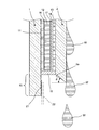
- FIG. 2 is a cross-sectional view of the main part of the liquid crystal panel of the first embodiment.
- the liquid crystal panel includes a liquid crystal layer 12 sealed between the TFT side glass substrate 1 and the CF side glass substrate 2 and a display area A1 along the peripheral portion of the TFT side glass substrate 1. And a sealing material 15 provided so as to surround (shown in FIG. 1).
- the liquid crystal layer 12 is sealed between the TFT side glass substrate 1 and the CF side glass substrate 2 by the sealing material 15.
- a plurality of thin film transistors 11 arranged in a matrix, a plurality of pixel electrodes (not shown), and an alignment film 16 are formed on one surface of the TFT side glass substrate 1 facing the CF side glass substrate 2. .
- a polarizing plate (not shown) is formed on the other surface of the TFT side glass substrate 1.
- a plurality of color filters 13 arranged in a matrix, a counter electrode 14, and an alignment film 17 are formed on one surface of the CF side glass substrate 2 facing the TFT side glass substrate 1.
- the RGB three color filters 13 are arranged for each pixel.
- a polarizing plate (not shown) is formed on the other surface of the CF side glass substrate 2.
- the lower end surface of the CF side glass substrate 2 is lower than the sealing material 15 and gradually lowers from one side facing the TFT side glass substrate 1 to the other side (panel surface) And the inclined surface 2a.
- the inclined surface 2a of the CF side glass substrate 2 has an angle ⁇ of 15 degrees to 45 degrees with respect to a plane parallel to the lower edge of the CF side glass substrate 2 and orthogonal to the CF side glass substrate 2.
- the liquid crystal panel of the first embodiment when the panel surface which is the front surface of the CF side glass substrate 2 (second glass substrate) is cleaned with a liquid W such as a cleaning liquid in a state of being incorporated in a display device, the liquid W Even if it flows down along the front surface of the side glass substrate 2, it drips from the tip of the panel surface side of the lower end surface of the CF side glass substrate 2, so the liquid W such as cleaning liquid is the lower end surface of the CF side glass substrate 2 and the sealing material 15 As a result, it does not come into contact with the overhang region 10 under the TFT side glass substrate 1.
- the liquid W such as a cleaning liquid is in contact with the lower overhanging region 10 of the TFT side glass substrate 1 when the panel surface is cleaned without applying the coating agent to the overhanging region 10.
- the lower end surface of the CF side glass substrate 2 is an inclined surface 2 a which is gradually lowered from one side facing the TFT side glass substrate 1 to the other side (panel surface) side. And the like can reliably be prevented from contacting the lower end surface of the CF side glass substrate 2 and the sealing material 15 and coming into contact with the lower overhanging region 10 of the TFT side glass substrate 1. Further, in the polishing process of the end face of the CF side glass substrate 2, the inclined surface 2a can be easily provided.
- the liquid such as the cleaning liquid is not affected by the sealing function of the sealing material 15, and the lower end face of the CF side glass substrate 2 and the sealing material It can be reliably prevented from flowing to the lower overhanging region 10 of the TFT side glass substrate 1 along the line 15.
- the inclined surface 2a at the lower end of the CF side glass substrate 2 may be roughened (for example, surface roughness 0.1 ⁇ m to 120 ⁇ m). In this case, the water repellency of the inclined surface 2a of the CF side glass substrate 2 is enhanced, and the effect of preventing the cleaning liquid and the like from being transmitted to the TFT side glass substrate 1 through the inclined surface 2a at the lower end of the CF side glass substrate 2 .
- ⁇ About surface roughness> (1) If the maximum height Rz representing the surface roughness is less than 0.1 ⁇ m, a convex-concave shape suitable for improving water repellency can not be formed, and the water repellency can not be sufficiently improved. (2) In order to sufficiently improve the water repellency, it is desirable to form a ten-point average roughness Rzjis 0.2 ⁇ m to 120 ⁇ m which represents the surface roughness. From the above (1) and (2), it is desirable that the surface roughness for sufficiently improving the water repellency has a shape of 0.1 ⁇ m to 120 ⁇ m (a condition that satisfies both Rz and Rzjis).
- the maximum height Rz and the ten-point average roughness Rzjis are defined as follows (JIS B 0601-2001).
- Rz Sum of the maximum value of the peak height of the contour curve and the maximum value of the valley depth at the reference length
- Rzjis Only the reference length is extracted from the roughness curve in the direction of its average line The sum of the average of the absolute values of the highest peaks from the highest peak to the fifth peak, and the average of the absolute values of the highest peaks of the lowest valley bottom to the fifth
- the mother glass may be cut into a second glass substrate of a predetermined size, and then the lower end face of the second glass substrate may be polished to form an inclined surface. You may form an inclined surface.
- FIG. 3 is a cross-sectional view of the main part of the liquid crystal panel according to the second embodiment of the present invention.
- the liquid crystal panel of the second embodiment has the same configuration as the liquid crystal panel of the first embodiment except for the lower end of the CF side glass substrate 2.
- the lower end surface of the CF side glass substrate 2 has a surface other than the one surface facing the TFT side glass substrate 1 (first glass substrate)
- the step portion 30 is provided so that the (panel surface) side is lowered.
- the liquid W such as the cleaning liquid is formed on the lower end surface and the seal of the CF side glass substrate 2 by providing the step portion 30 on the lower end surface of the CF side glass substrate 2 (second glass substrate).
- the material 15 can be reliably prevented from coming into contact with the lower overhanging region 10 of the TFT side glass substrate 1.
- the liquid crystal panel of the second embodiment has the same effect as the liquid crystal panel of the first embodiment.
- FIG. 4 is a cross-sectional view of the main part of the liquid crystal panel according to the third embodiment of the present invention.
- the liquid crystal panel of the second embodiment has the same configuration as the liquid crystal panel of the first embodiment except for the bezel 40.
- the liquid crystal panel of the third embodiment includes a bezel 40 which covers the outside of the display area A1 of the surface of the second glass substrate 2 opposite to the first glass substrate 1.
- the bezel 40 holds the CF side glass substrate 2.
- the liquid W such as the cleaning liquid which has fallen along the front surface of the second glass substrate 2 is guided downward along the front surface of the second glass substrate 2 by the bezel 40.
- the liquid W such as the cleaning liquid can be reliably prevented from entering the lower overhanging region 10 of the first glass substrate 1 in combination with the inclined surface 2 a at the lower end of the first glass substrate 1.
- the liquid crystal panel of the third embodiment has the same effect as the liquid crystal panel of the first embodiment.
- the liquid crystal panel according to one aspect of the present invention is A first glass substrate 1; A second glass substrate 2 having a display area A1 on the front surface and spaced apart from the first glass substrate 1 so that the rear surface faces the first glass substrate 1; A liquid crystal layer 12 sealed between the first glass substrate 1 and the second glass substrate 2;
- the first glass substrate 1 has an overhanging area 10 projecting downward below the lower end of the second glass substrate 2, and a terminal portion 21 provided on the second glass substrate 2 side of the overhanging area 10.
- Have The lower end surface of the second glass substrate 2 is characterized in that the front surface side of the second glass substrate 2 is lower than the rear surface side of the second glass substrate 2.
- the lower end surface of the second glass substrate 2 when the front surface of the second glass substrate 2 is cleaned with a liquid such as a cleaning liquid, the lower end surface of the second glass substrate 2 even if the liquid such as the cleaning liquid flows down along the front surface of the second glass substrate 2
- a liquid such as a cleaning liquid drips from the tip (front side) of the lower end surface of the second glass substrate 2.
- the second glass substrate 2 does not flow along the lower end surface of the second glass substrate 2 into the lower overhanging region 10 of the first glass substrate 1. Therefore, it is possible to prevent the liquid such as the cleaning liquid from coming into contact with the lower overhanging area 10 of the first glass substrate 1 when cleaning the panel surface without applying the coating agent, and it is possible to suppress the occurrence of display defects.
- the lower end surface of the second glass substrate 2 is an inclined surface 2 a which is gradually lowered from the rear surface side of the second glass substrate 2 toward the front surface side of the second glass substrate 2.
- the lower end surface of the second glass substrate 2 is set to the inclined surface 2 a which is gradually lowered from the rear surface side of the second glass substrate 2 toward the front surface side of the second glass substrate 2.
- the liquid such as the cleaning liquid can be reliably prevented from flowing along the lower end surface of the second glass substrate 2 and flowing into the lower overhanging region 10 of the first glass substrate 1 and polishing of the end surface of the second glass substrate 2 In the process, the inclined surface 2a can be easily provided.
- the lower end surface of the second glass substrate 2 is a rough surface rougher than the other side surface of the second glass substrate 2.
- the water repellency of the inclined surface 2a of the second glass substrate 2 is enhanced, and the cleaning liquid and the like are prevented from being transmitted to the first glass substrate 1 through the inclined surface 2a at the lower end of the second glass substrate 2 The effect is higher.
- a stepped portion 30 is provided on the lower end surface of the second glass substrate 2 so that the front surface side of the second glass substrate 2 is lower than the rear surface side of the second glass substrate 2.
- the front surface of the second glass substrate 2 is more than the rear surface side of the second glass substrate 2 at the lower end surface of the second glass substrate 2. Since the side is lowered, it is possible to reliably prevent the liquid such as the cleaning liquid from flowing along the lower end surface of the second glass substrate 2 and flowing into the lower overhanging region 10 of the first glass substrate 1.
- a sealing material 15 is provided along the periphery of the first glass substrate 1 and for sealing the liquid crystal layer 12 between the first glass substrate 1 and the second glass substrate 2;
- the lower end surface of the second glass substrate 2 is lower than the sealing material 15.
- the liquid such as the cleaning liquid can be removed from the second glass substrate 2 without impairing the sealing function of the sealing material 15. It can be reliably prevented from flowing along the lower end surface and into the lower overhanging region 10 of the first glass substrate 1.
- a bezel 40 is provided to cover the outside of the display area A1 of the front surface of the second glass substrate 2.
- the bezel 40 that covers the outside of the display area A1 of the front surface of the second glass substrate 2, the liquid such as the cleaning liquid that has fallen along the front surface of the second glass substrate 2 is the bezel 40 As a result of being guided downward, it is possible, with the shape of the lower end face of the second glass substrate 2, to reliably prevent the entry of a liquid such as a cleaning liquid into the lower overhanging region 10 of the first glass substrate 1.
Landscapes
- Physics & Mathematics (AREA)
- Nonlinear Science (AREA)
- Mathematical Physics (AREA)
- Chemical & Material Sciences (AREA)
- Crystallography & Structural Chemistry (AREA)
- General Physics & Mathematics (AREA)
- Optics & Photonics (AREA)
- Liquid Crystal (AREA)
- Devices For Indicating Variable Information By Combining Individual Elements (AREA)
Abstract
液晶パネルは、第1ガラス基板(1)と、前面に表示領域を有し、後面が第1ガラス基板(1)の前面側に対向するように第1ガラス基板(1)に対して間隔をあけて配置された第2ガラス基板(2)と、第1ガラス基板(1)と第2ガラス基板(2)との間に封止された液晶層(12)とを備える。第1ガラス基板(1)は、第2ガラス基板(2)の下端よりも下側に張り出した張出領域(10)と、張出領域(10)の第2ガラス基板(2)側に設けられた端子部21とを有する。第2ガラス基板(2)の下端面は、第2ガラス基板(2)の後面側よりも第2ガラス基板(2)の前面側が低くなっている。これにより、コーティング剤を塗布することなく、パネル面の洗浄時に洗浄液などの液体が第1ガラス基板(1)の下側の張出領域(10)に接触しないようにすることで、表示不良の発生を抑制できる液晶パネルを提供する。
Description
この発明は、液晶パネルに関する。
従来、液晶パネルとしては、薄膜トランジスタが形成された第1ガラス基板と、カラーフィルタが形成された第2ガラス基板との間に液晶層を封止し、その液晶を封止するためのシール材を第1ガラス基板と第2ガラス基板との間に設けたものがある(例えば、国際公開第2016/098232号(特許文献1)参照)。
上記従来の液晶パネルでは、TV(テレビジョン)などのディスプレイ装置に組み込まれた状態で第2ガラス基板の下端面が略水平となるため、ディスプレイ装置のパネル面(第2ガラス基板の前面)を洗浄液で洗うときに、洗浄液がパネル面に沿って流れ落ちて、第2ガラス基板の下端面およびシール材を伝って、第1ガラス基板の下側の張出領域に流れ込んで滞留する場合がある。
このような場合、液晶パネルの第1ガラス基板の下側の張出領域に接触した洗浄液が、第1ガラス基板の張出領域に設けられた端子部の電極間において短絡を誘発することで、表示不良が発生するという問題がある。
このため、上記従来の液晶パネルでは、第1ガラス基板の下側の張出領域にコーティング剤を塗布して防水対策を行ったりしているが、作業工程が増えて製造コストが高くなる。
そこで、この発明の課題は、コーティング剤を塗布することなく、パネル面の洗浄時に洗浄液などの液体がガラス基板の下側の張出領域に接触しないようにすることで、表示不良の発生を抑制できる液晶パネルを提供することにある。
この発明の一態様に係る液晶パネルは、
第1ガラス基板と、
前面に表示領域を有し、後面が上記第1ガラス基板に対向するように上記第1ガラス基板に対して間隔をあけて配置された第2ガラス基板と、
上記第1ガラス基板と上記第2ガラス基板との間に封止された液晶層と
を備え、
上記第1ガラス基板は、上記第2ガラス基板の下端よりも下側に張り出した張出領域と、上記張出領域の上記第2ガラス基板側に設けられた端子部とを有し、
上記第2ガラス基板の下端面は、上記第2ガラス基板の後面側よりも上記第2ガラス基板の前面側が低くなっていることを特徴とする。
第1ガラス基板と、
前面に表示領域を有し、後面が上記第1ガラス基板に対向するように上記第1ガラス基板に対して間隔をあけて配置された第2ガラス基板と、
上記第1ガラス基板と上記第2ガラス基板との間に封止された液晶層と
を備え、
上記第1ガラス基板は、上記第2ガラス基板の下端よりも下側に張り出した張出領域と、上記張出領域の上記第2ガラス基板側に設けられた端子部とを有し、
上記第2ガラス基板の下端面は、上記第2ガラス基板の後面側よりも上記第2ガラス基板の前面側が低くなっていることを特徴とする。
この発明によれば、コーティング剤を塗布することなく、洗浄液などの液体がガラス基板の下側の張出領域に接触しないようにすることで、表示不良の発生を抑制できる液晶パネルを実現することができる。
以下、この発明の液晶パネルを図示の実施の形態により詳細に説明する。複数の図面を通じて、同一の構成要素には同一の符号を付している。
〔第1実施形態〕
図1は、この発明の第1実施形態の液晶パネルの正面図である。
図1は、この発明の第1実施形態の液晶パネルの正面図である。
この第1実施形態の液晶パネルは、図1に示すように、TFT(Thin Film Transistor:薄膜トランジスタ)側ガラス基板1、TFT側ガラス基板1の前面側に対向するようにTFT側ガラス基板1に対して間隔をあけて配置されたCF(Color Filter:カラーフィルタ)側ガラス基板2とを備えている。TFT側ガラス基板1は、第1ガラス基板の一例であり、CF側ガラス基板2の下端よりも下側に張り出した張出領域10を有する。張出領域10のCF側ガラス基板2側の面に端子部21(図2に示す)を設けている。張出領域10の端子部21に、ソースドライバ(図示せず)が実装されたフレキシブル基板22の電極が電気的に接続される。また、CF側ガラス基板2は、第2ガラス基板の一例である。
TFT側ガラス基板1およびCF側ガラス基板2の厚さを夫々、0.5mm~0.7mmとしている。
液晶パネルは、表示画素がマトリックス状に配列された表示領域A1と、表示領域A1の左右両側に配置された領域A2,A3とを有する。この領域A2,A3の双方またはいずれか一方は、ゲートドライバ回路が形成されたGOA(Gate On Array)領域である。
図2は、第1実施形態の液晶パネルの要部の断面図である。
図2に示すように、液晶パネルは、TFT側ガラス基板1とCF側ガラス基板2との間に封止された液晶層12と、TFT側ガラス基板1の周縁部に沿って表示領域A1(図1に示す)を囲むように設けられたシール材15とを備えている。シール材15によって、TFT側ガラス基板1とCF側ガラス基板2との間に液晶層12が封止されている。
TFT側ガラス基板1のCF側ガラス基板2に対向する一の面には、マトリックス状に配列された複数の薄膜トランジスタ11と複数の画素電極(図示せず)と配向膜16とが形成されている。一方、TFT側ガラス基板1の他の面には、偏光板(図示せず)が形成されている。
また、CF側ガラス基板2のTFT側ガラス基板1に対向する一の面には、マトリックス状に配置された複数のカラーフィルタ13と対向電極14と配向膜17とが形成されている。RGB三色のカラーフィルタ13が画素毎に配列されている。一方、CF側ガラス基板2の他の面には、偏光板(図示せず)が形成されている。
CF側ガラス基板2の下端面は、シール材15よりも下側であって、かつ、TFT側ガラス基板1に対向する一の面側から他の面(パネル面)に向かって徐々に低くなった傾斜面2aである。このCF側ガラス基板2の傾斜面2aは、CF側ガラス基板2の下縁に平行かつCF側ガラス基板2に直交する平面に対する角度θを15deg~45degとしている。
第1実施形態の液晶パネルでは、ディスプレイ装置に組み込まれた状態でCF側ガラス基板2(第2ガラス基板)の前面であるパネル面を洗浄液などの液体Wで洗浄するとき、その液体WがCF側ガラス基板2の前面に沿って流れ落ちても、CF側ガラス基板2の下端面のパネル面側の先端から滴り落ちるので、洗浄液などの液体WがCF側ガラス基板2の下端面およびシール材15を伝わって、TFT側ガラス基板1の下側の張出領域10に接触するようなことがない。
したがって、第1実施形態の液晶パネルでは、張出領域10にコーティング剤を塗布することなく、パネル面の洗浄時に洗浄液などの液体WがTFT側ガラス基板1の下側の張出領域10に接触しないようにして、表示不良の発生を抑制することができる。
さらに、CF側ガラス基板2の下端面を、TFT側ガラス基板1に対向する一の面側から他の面(パネル面)側に向かって徐々に低くなった傾斜面2aとすることにより、洗浄液などの液体WがCF側ガラス基板2の下端面およびシール材15を伝わってTFT側ガラス基板1の下側の張出領域10に接触するのを確実に防ぐことができる。また、CF側ガラス基板2の端面の研磨工程において、傾斜面2aを容易に設けることができる。
また、CF側ガラス基板2の下端面をシール材15よりも下側にすることで、シール材15のシール機能を損なうことなく、洗浄液などの液体がCF側ガラス基板2の下端面およびシール材15を伝わってTFT側ガラス基板1の下側の張出領域10に流れ込むのを確実に防ぐことができる。
また、第1実施形態において、CF側ガラス基板2の下端の傾斜面2aを粗面(例えば表面粗さ0.1μm~120μm)にしてもよい。この場合、CF側ガラス基板2の傾斜面2aの撥水性が高まり、洗浄液などがCF側ガラス基板2の下端の傾斜面2aを介してTFT側ガラス基板1側に伝わるのを妨げる効果が高くなる。
<表面粗さについて>
(1) 表面粗さを表す最大高さRzが0.1μm未満の場合には、撥水性向上のために適した凸凹形状が形成できず、十分に撥水性を向上させることができない。
(2) 十分に撥水性を向上させるには、表面粗さを表す十点平均粗さRzjis=0.2μm~120μmで形成するのが望ましい。
上記(1),(2)から十分に撥水性を向上させるための表面粗さは、0.1μm~120μmの形状が望ましい(RzとRzjisのどちらも満たす条件)。
(1) 表面粗さを表す最大高さRzが0.1μm未満の場合には、撥水性向上のために適した凸凹形状が形成できず、十分に撥水性を向上させることができない。
(2) 十分に撥水性を向上させるには、表面粗さを表す十点平均粗さRzjis=0.2μm~120μmで形成するのが望ましい。
上記(1),(2)から十分に撥水性を向上させるための表面粗さは、0.1μm~120μmの形状が望ましい(RzとRzjisのどちらも満たす条件)。
なお、最大高さRzと十点平均粗さRzjisは、次の通り定義される(JIS B 0601-2001)。
Rz : 基準長さにおいて、輪郭曲線の山高さの最大値と谷深さの最大値の和
Rzjis: 粗さ曲線から、その平均線の方向に基準長さだけを抜き取り、この抜き取り部分の平均線から、最も高い山頂から5番目までの山頂の標高の絶対値の平均値と、最も低い谷底から5番目までの谷底の標高の絶対値の平均値との和
Rz : 基準長さにおいて、輪郭曲線の山高さの最大値と谷深さの最大値の和
Rzjis: 粗さ曲線から、その平均線の方向に基準長さだけを抜き取り、この抜き取り部分の平均線から、最も高い山頂から5番目までの山頂の標高の絶対値の平均値と、最も低い谷底から5番目までの谷底の標高の絶対値の平均値との和
第1実施形態では、マザーガラスを所定のサイズの第2ガラス基板にカッティングした後、第2ガラス基板の下端面を研磨することにより傾斜面を形成してもよいし、マザーガラスのカッティングと同時に傾斜面を形成してもよい。
〔第2実施形態〕
図3は、この発明の第2実施形態の液晶パネルの要部の断面図である。この第2実施形態の液晶パネルは、CF側ガラス基板2の下端を除いて第1実施形態の液晶パネルと同一の構成をしている。
図3は、この発明の第2実施形態の液晶パネルの要部の断面図である。この第2実施形態の液晶パネルは、CF側ガラス基板2の下端を除いて第1実施形態の液晶パネルと同一の構成をしている。
この第2実施形態の液晶パネルは、図3に示すように、CF側ガラス基板2の下端面に、TFT側ガラス基板1(第1ガラス基板)に対向する一の面側よりも他の面(パネル面)側が低くなるように段差部30を設けている。
第2実施形態の液晶パネルによれば、CF側ガラス基板2(第2ガラス基板)の下端面に段差部30を設けることにより、洗浄液などの液体WがCF側ガラス基板2の下端面およびシール材15を伝わってTFT側ガラス基板1の下側の張出領域10に接触するのを確実に防ぐことができる。
この第2実施形態の液晶パネルは、第1実施形態の液晶パネルと同様の効果を有する。
〔第3実施形態〕
図4は、この発明の第3実施形態の液晶パネルの要部の断面図である。この第2実施形態の液晶パネルは、ベゼル40を除いて第1実施形態の液晶パネルと同一の構成をしている。
図4は、この発明の第3実施形態の液晶パネルの要部の断面図である。この第2実施形態の液晶パネルは、ベゼル40を除いて第1実施形態の液晶パネルと同一の構成をしている。
この第3実施形態の液晶パネルは、図4に示すように、第2ガラス基板2の第1ガラス基板1と反対の側の面のうちの表示領域A1の外側を覆うベゼル40を備える。ベゼル40は、CF側ガラス基板2を保持している。
第3実施形態の液晶パネルによれば、ベゼル40によって、第2ガラス基板2の前面に沿って流れ落ちた洗浄液などの液体Wがベゼル40を伝って下方に案内されるので、CF側ガラス基板2の下端の傾斜面2aと相まって、第1ガラス基板1の下側の張出領域10への洗浄液などの液体Wの浸入を確実に防止することができる。
この第3実施形態の液晶パネルは、第1実施形態の液晶パネルと同様の効果を有する。
この発明の具体的な実施の形態について説明したが、この発明は第1~第3実施形態に限定されるものではなく、この発明の範囲内で種々変更して実施することができる。
この発明および実施形態をまとめると、次のようになる。
この発明の一態様に係る液晶パネルは、
第1ガラス基板1と、
前面に表示領域A1を有し、後面が上記第1ガラス基板1に対向するように上記第1ガラス基板1に対して間隔をあけて配置された第2ガラス基板2と、
上記第1ガラス基板1と上記第2ガラス基板2との間に封止された液晶層12と
を備え、
上記第1ガラス基板1は、上記第2ガラス基板2の下端よりも下側に張り出した張出領域10と、上記張出領域10の上記第2ガラス基板2側に設けられた端子部21とを有し、
上記第2ガラス基板2の下端面は、上記第2ガラス基板2の後面側よりも上記第2ガラス基板2の前面側が低くなっていることを特徴とする。
第1ガラス基板1と、
前面に表示領域A1を有し、後面が上記第1ガラス基板1に対向するように上記第1ガラス基板1に対して間隔をあけて配置された第2ガラス基板2と、
上記第1ガラス基板1と上記第2ガラス基板2との間に封止された液晶層12と
を備え、
上記第1ガラス基板1は、上記第2ガラス基板2の下端よりも下側に張り出した張出領域10と、上記張出領域10の上記第2ガラス基板2側に設けられた端子部21とを有し、
上記第2ガラス基板2の下端面は、上記第2ガラス基板2の後面側よりも上記第2ガラス基板2の前面側が低くなっていることを特徴とする。
上記構成によれば、第2ガラス基板2の前面を洗浄液などの液体で洗浄するとき、第2ガラス基板2の前面に沿って洗浄液などの液体が流れ落ちても、第2ガラス基板2の下端面が、第2ガラス基板2の後側よりも第2ガラス基板2の前側が低くなっていることによって、洗浄液などの液体が第2ガラス基板2の下端面の先端(前面側)から滴り落ちるので、第2ガラス基板2の下端面を伝わって、第1ガラス基板1の下側の張出領域10に流れ込むことがない。したがって、コーティング剤を塗布することなく、パネル面の洗浄時に洗浄液などの液体が第1ガラス基板1の下側の張出領域10に接触しないようにでき、表示不良の発生を抑制できる。
また、一実施形態の液晶パネルでは、
上記第2ガラス基板2の下端面は、上記第2ガラス基板2の後面側から上記第2ガラス基板2の前面側に向かって徐々に低くなった傾斜面2aである。
上記第2ガラス基板2の下端面は、上記第2ガラス基板2の後面側から上記第2ガラス基板2の前面側に向かって徐々に低くなった傾斜面2aである。
上記実施形態によれば、第2ガラス基板2の下端面を、第2ガラス基板2の後面側から第2ガラス基板2の前面側に向かって徐々に低くなった傾斜面2aとすることにより、洗浄液などの液体が第2ガラス基板2の下端面を伝わって第1ガラス基板1の下側の張出領域10に流れ込むのを確実に防ぐことができると共に、第2ガラス基板2の端面の研磨工程において、傾斜面2aを容易に設けることができる。
また、一実施形態の液晶パネルでは、
上記第2ガラス基板2の下端面は、上記第2ガラス基板2の他の側面よりも粗い粗面である。
上記第2ガラス基板2の下端面は、上記第2ガラス基板2の他の側面よりも粗い粗面である。
上記実施形態によれば、第2ガラス基板2の傾斜面2aの撥水性が高まり、洗浄液などが第2ガラス基板2の下端の傾斜面2aを介して第1ガラス基板1側に伝わるのを妨げる効果が高くなる。
また、一実施形態の液晶パネルでは、
上記第2ガラス基板2の下端面に、上記第2ガラス基板2の後面側よりも上記第2ガラス基板2の前面側が低くなるように段差部30を設けた。
上記第2ガラス基板2の下端面に、上記第2ガラス基板2の後面側よりも上記第2ガラス基板2の前面側が低くなるように段差部30を設けた。
上記実施形態によれば、第2ガラス基板2の下端面に段差部30を設けることにより、第2ガラス基板2の下端面において第2ガラス基板2の後面側よりも第2ガラス基板2の前面側が低くなるので、洗浄液などの液体が第2ガラス基板2の下端面を伝わって第1ガラス基板1の下側の張出領域10に流れ込むのを確実に防ぐことができる。
また、一実施形態の液晶パネルでは、
上記第1ガラス基板1の周縁部に沿って設けられ、上記第1ガラス基板1と上記第2ガラス基板2との間に上記液晶層12を封止するためのシール材15を備え、
上記第2ガラス基板2の下端面は、上記シール材15よりも下側である。
上記第1ガラス基板1の周縁部に沿って設けられ、上記第1ガラス基板1と上記第2ガラス基板2との間に上記液晶層12を封止するためのシール材15を備え、
上記第2ガラス基板2の下端面は、上記シール材15よりも下側である。
上記実施形態によれば、第2ガラス基板2の下端面をシール材15よりも下側にすることで、シール材15のシール機能を損なうことなく、洗浄液などの液体が第2ガラス基板2の下端面およびを伝わって第1ガラス基板1の下側の張出領域10に流れ込むのを確実に防ぐことができる。
また、一実施形態の液晶パネルでは、
上記第2ガラス基板2の前面のうちの上記表示領域A1の外側を覆うベゼル40を備える。
上記第2ガラス基板2の前面のうちの上記表示領域A1の外側を覆うベゼル40を備える。
上記実施形態によれば、第2ガラス基板2の前面のうちの表示領域A1の外側を覆うベゼル40を備えることによって、第2ガラス基板2の前面に沿って流れ落ちた洗浄液などの液体がベゼル40を伝って下方に案内されるので、第2ガラス基板2の下端面の形状と相まって、第1ガラス基板1の下側の張出領域10への洗浄液などの液体の浸入を確実に防止できる。
1…TFT側ガラス基板(第1ガラス基板)
2…CF側ガラス基板(第2ガラス基板)
2a…傾斜面
10…張出領域
11…薄膜トランジスタ
12…液晶層
13…カラーフィルタ
14…対向電極
15…シール材
16,17…配向膜
21…端子部
22…フレキシブル基板
30…段差部
40…ベゼル
A1…表示領域
A2,A3…領域
2…CF側ガラス基板(第2ガラス基板)
2a…傾斜面
10…張出領域
11…薄膜トランジスタ
12…液晶層
13…カラーフィルタ
14…対向電極
15…シール材
16,17…配向膜
21…端子部
22…フレキシブル基板
30…段差部
40…ベゼル
A1…表示領域
A2,A3…領域
Claims (6)
- 第1ガラス基板と、
前面に表示領域を有し、後面が上記第1ガラス基板に対向するように上記第1ガラス基板に対して間隔をあけて配置された第2ガラス基板と、
上記第1ガラス基板と上記第2ガラス基板との間に封止された液晶層と
を備え、
上記第1ガラス基板は、上記第2ガラス基板の下端よりも下側に張り出した張出領域と、上記張出領域の上記第2ガラス基板側に設けられた端子部とを有し、
上記第2ガラス基板の下端面は、上記第2ガラス基板の後面側よりも上記第2ガラス基板の前面側が低くなっていることを特徴とする液晶パネル。 - 請求項1に記載の液晶パネルにおいて、
上記第2ガラス基板の下端面は、上記第2ガラス基板の後面側から上記第2ガラス基板の前面側に向かって徐々に低くなった傾斜面であることを特徴とする液晶パネル。 - 請求項1または2に記載の液晶パネルにおいて、
上記第2ガラス基板の下端面は、上記第2ガラス基板の他の側面よりも粗い粗面であることを特徴とする液晶パネル。 - 請求項1に記載の液晶パネルにおいて、
上記第2ガラス基板の下端面に、上記第2ガラス基板の後面側よりも上記第2ガラス基板の前面側が低くなるように段差部を設けたことを特徴とする液晶パネル。 - 請求項1から4までのいずれか1つに記載の液晶パネルにおいて、
上記第1ガラス基板の周縁部に沿って設けられ、上記第1ガラス基板と上記第2ガラス基板との間に上記液晶層を封止するためのシール材を備え、
上記第2ガラス基板の下端面は、上記シール材よりも下側であることを特徴とする液晶パネル。 - 請求項1から5までのいずれか1つに記載の液晶パネルにおいて、
上記第2ガラス基板の前面のうちの上記表示領域の外側を覆うベゼルを備えることを特徴とする液晶パネル。
Priority Applications (1)
| Application Number | Priority Date | Filing Date | Title |
|---|---|---|---|
| PCT/JP2017/046848 WO2019130461A1 (ja) | 2017-12-27 | 2017-12-27 | 液晶パネル |
Applications Claiming Priority (1)
| Application Number | Priority Date | Filing Date | Title |
|---|---|---|---|
| PCT/JP2017/046848 WO2019130461A1 (ja) | 2017-12-27 | 2017-12-27 | 液晶パネル |
Publications (1)
| Publication Number | Publication Date |
|---|---|
| WO2019130461A1 true WO2019130461A1 (ja) | 2019-07-04 |
Family
ID=67066830
Family Applications (1)
| Application Number | Title | Priority Date | Filing Date |
|---|---|---|---|
| PCT/JP2017/046848 Ceased WO2019130461A1 (ja) | 2017-12-27 | 2017-12-27 | 液晶パネル |
Country Status (1)
| Country | Link |
|---|---|
| WO (1) | WO2019130461A1 (ja) |
Citations (6)
| Publication number | Priority date | Publication date | Assignee | Title |
|---|---|---|---|---|
| JPS6012528A (ja) * | 1983-07-01 | 1985-01-22 | Hitachi Ltd | 液晶表示素子 |
| JP2003015112A (ja) * | 2001-06-29 | 2003-01-15 | Hitachi Ltd | 液晶表示素子およびその製造方法ならびに製造装置 |
| JP2011209385A (ja) * | 2010-03-29 | 2011-10-20 | Seiko Epson Corp | 液晶装置、液晶装置の駆動方法及び電子機器 |
| JP2013068895A (ja) * | 2011-09-26 | 2013-04-18 | Japan Display East Co Ltd | 液晶表示装置 |
| JP2014157311A (ja) * | 2013-02-18 | 2014-08-28 | Japan Display Inc | 表示装置および表示装置の製造方法 |
| US20170003540A1 (en) * | 2015-07-03 | 2017-01-05 | Au Optronics Corp. | Display device and manufacturing method thereof |
-
2017
- 2017-12-27 WO PCT/JP2017/046848 patent/WO2019130461A1/ja not_active Ceased
Patent Citations (6)
| Publication number | Priority date | Publication date | Assignee | Title |
|---|---|---|---|---|
| JPS6012528A (ja) * | 1983-07-01 | 1985-01-22 | Hitachi Ltd | 液晶表示素子 |
| JP2003015112A (ja) * | 2001-06-29 | 2003-01-15 | Hitachi Ltd | 液晶表示素子およびその製造方法ならびに製造装置 |
| JP2011209385A (ja) * | 2010-03-29 | 2011-10-20 | Seiko Epson Corp | 液晶装置、液晶装置の駆動方法及び電子機器 |
| JP2013068895A (ja) * | 2011-09-26 | 2013-04-18 | Japan Display East Co Ltd | 液晶表示装置 |
| JP2014157311A (ja) * | 2013-02-18 | 2014-08-28 | Japan Display Inc | 表示装置および表示装置の製造方法 |
| US20170003540A1 (en) * | 2015-07-03 | 2017-01-05 | Au Optronics Corp. | Display device and manufacturing method thereof |
Similar Documents
| Publication | Publication Date | Title |
|---|---|---|
| KR102242439B1 (ko) | 곡면형 액정 표시 장치 | |
| WO2019047461A1 (zh) | 液晶面板及其制作方法 | |
| US20210223587A1 (en) | Method for manufacturing display panel and display panel | |
| JP2000227596A (ja) | 液晶表示装置 | |
| CN104456327B (zh) | 一种背光模组和显示装置 | |
| JP2011164596A (ja) | 液晶表示装置 | |
| JP2017111290A (ja) | 液晶表示装置 | |
| CN100470342C (zh) | 共平面开关模式液晶显示器件及其制造方法 | |
| JP2014182163A (ja) | 表示装置 | |
| CN106646966A (zh) | 显示装置 | |
| JP2010122333A (ja) | 液晶表示装置 | |
| US9507207B2 (en) | Display device | |
| TW201917456A (zh) | 顯示裝置 | |
| WO2017177667A1 (zh) | 液晶显示面板及显示装置 | |
| JP2017116797A (ja) | 液晶表示装置 | |
| TW200528883A (en) | Liquid crystal display apparatus and method for manufacturing the same | |
| TWI544252B (zh) | 顯示面板及其製造方法 | |
| CN203224698U (zh) | 一种液晶面板及显示装置 | |
| TW201823813A (zh) | 顯示面板 | |
| JP2020034727A (ja) | 液晶表示装置 | |
| JP2008089994A (ja) | 画像表示装置およびその製造方法 | |
| JP5403539B2 (ja) | 横電界方式の液晶表示装置 | |
| US20110051067A1 (en) | Liquid crystal display device and printing plate for orientation film | |
| WO2013091437A1 (zh) | 液晶显示装置、阵列基板及其制造方法 | |
| JP2009192660A (ja) | 表示装置 |
Legal Events
| Date | Code | Title | Description |
|---|---|---|---|
| 121 | Ep: the epo has been informed by wipo that ep was designated in this application |
Ref document number: 17935909 Country of ref document: EP Kind code of ref document: A1 |
|
| NENP | Non-entry into the national phase |
Ref country code: DE |
|
| 122 | Ep: pct application non-entry in european phase |
Ref document number: 17935909 Country of ref document: EP Kind code of ref document: A1 |
|
| NENP | Non-entry into the national phase |
Ref country code: JP |