WO2019106966A1 - 表示装置 - Google Patents
表示装置 Download PDFInfo
- Publication number
- WO2019106966A1 WO2019106966A1 PCT/JP2018/037575 JP2018037575W WO2019106966A1 WO 2019106966 A1 WO2019106966 A1 WO 2019106966A1 JP 2018037575 W JP2018037575 W JP 2018037575W WO 2019106966 A1 WO2019106966 A1 WO 2019106966A1
- Authority
- WO
- WIPO (PCT)
- Prior art keywords
- unit
- electrode
- detection
- display
- display device
- Prior art date
- Legal status (The legal status is an assumption and is not a legal conclusion. Google has not performed a legal analysis and makes no representation as to the accuracy of the status listed.)
- Ceased
Links
Images



Classifications
-
- H—ELECTRICITY
- H10—SEMICONDUCTOR DEVICES; ELECTRIC SOLID-STATE DEVICES NOT OTHERWISE PROVIDED FOR
- H10K—ORGANIC ELECTRIC SOLID-STATE DEVICES
- H10K59/00—Integrated devices, or assemblies of multiple devices, comprising at least one organic light-emitting element covered by group H10K50/00
- H10K59/40—OLEDs integrated with touch screens
-
- G—PHYSICS
- G06—COMPUTING OR CALCULATING; COUNTING
- G06F—ELECTRIC DIGITAL DATA PROCESSING
- G06F3/00—Input arrangements for transferring data to be processed into a form capable of being handled by the computer; Output arrangements for transferring data from processing unit to output unit, e.g. interface arrangements
- G06F3/01—Input arrangements or combined input and output arrangements for interaction between user and computer
- G06F3/03—Arrangements for converting the position or the displacement of a member into a coded form
- G06F3/041—Digitisers, e.g. for touch screens or touch pads, characterised by the transducing means
-
- G—PHYSICS
- G06—COMPUTING OR CALCULATING; COUNTING
- G06F—ELECTRIC DIGITAL DATA PROCESSING
- G06F3/00—Input arrangements for transferring data to be processed into a form capable of being handled by the computer; Output arrangements for transferring data from processing unit to output unit, e.g. interface arrangements
- G06F3/01—Input arrangements or combined input and output arrangements for interaction between user and computer
- G06F3/03—Arrangements for converting the position or the displacement of a member into a coded form
- G06F3/041—Digitisers, e.g. for touch screens or touch pads, characterised by the transducing means
- G06F3/044—Digitisers, e.g. for touch screens or touch pads, characterised by the transducing means by capacitive means
-
- G—PHYSICS
- G09—EDUCATION; CRYPTOGRAPHY; DISPLAY; ADVERTISING; SEALS
- G09F—DISPLAYING; ADVERTISING; SIGNS; LABELS OR NAME-PLATES; SEALS
- G09F9/00—Indicating arrangements for variable information in which the information is built-up on a support by selection or combination of individual elements
-
- G—PHYSICS
- G09—EDUCATION; CRYPTOGRAPHY; DISPLAY; ADVERTISING; SEALS
- G09F—DISPLAYING; ADVERTISING; SIGNS; LABELS OR NAME-PLATES; SEALS
- G09F9/00—Indicating arrangements for variable information in which the information is built-up on a support by selection or combination of individual elements
- G09F9/30—Indicating arrangements for variable information in which the information is built-up on a support by selection or combination of individual elements in which the desired character or characters are formed by combining individual elements
Definitions
- the present invention relates to a display device.
- Patent Document 1 has a winding unit that winds a part or all of a display unit including a touch panel, and a detection unit that detects a wound area, and the wound area of the touch panel Disclosed is a display device for stopping the operation.
- a dedicated detection unit is provided to detect a wound area.
- the internal structure of the image display device becomes complicated.
- the present invention has been made in view of the above problems, and an object thereof is to provide a compact display device having a simple configuration, which does not require a dedicated detection electrode for detecting the state of the touch panel. .
- One embodiment of the present invention is a display device including a display unit provided with a touch panel, and a storage unit, wherein the storage unit stores a part or all of the display unit, and the touch panel is configured to A plurality of pairs of a main drive electrode and a detection electrode which are spaced apart in the storing direction and mutually form a main capacitance, a detection unit which detects a voltage of the detection electrode, and the main capacitance
- a drive unit for supplying a main drive signal for changing the voltage of the detection electrode to the main drive electrode, and a control unit for controlling the operation of the detection unit and the drive unit
- the display device further comprising: A plurality of pairs are provided so as to be positioned on the front or back of a part according to the storage state of the display unit, and an additional capacitance is formed between the pair and the detection electrode according to the storage state An additional drive electrode, said drive unit An additional drive signal for changing the voltage of the detection electrode through the additional capacitance to the additional drive electrode, and the control unit further causes
- the case of the organic EL display device is exemplified as the disclosed example, but as another application example, a liquid crystal display device, another self-luminous display device, or an electron having an electrophoretic element or the like
- a liquid crystal display device such as a liquid crystal display device, another self-luminous display device, or an electron having an electrophoretic element or the like
- various flat panel type display devices such as a paper type display device. Further, it is needless to say that the invention can be applied to medium to small size and large size without particular limitation.
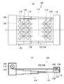
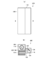
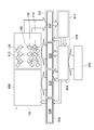
- FIGS. 1A, 2A, and 3A are plan views of the display device 100 as viewed from the top.
- FIG. 1 (b) is a cross-sectional view taken along line II of FIG. 1 (a).
- FIG. 2 (b) is a view showing a cross section II-II in FIG. 2 (a).
- FIG. 3 (b) is a cross-sectional view taken along the line III-III in FIG. 3 (a).
- FIGS. 1A and 1B are diagrams showing a state in which the display unit 102 is all pulled out from the first storage unit 106.
- FIGS. 2A and 2B are diagrams showing a state in which the display unit 102 is partially pulled out of the first storage unit 106.
- FIGS. 3A and 3B are diagrams showing a state in which all the display units 102 are stored in the first storage unit 106.
- FIG. 1A and 1B are diagrams showing a state in which the display unit 102 is all pulled out from the first storage unit 106.
- FIGS. 2A and 2B are diagrams showing a state in which the display unit 102 is partially pulled out of the first storage unit 106.
- FIGS. 3A and 3B are diagrams showing a state in which all the display units 102 are stored in the first storage unit 106.
- the display device 100 includes a display unit 102 provided with a touch panel 104, a first storage unit 106, a second storage unit 116, and a drawer structure 114.
- the display unit 102 includes a display area 128, a drive circuit 122 disposed outside the display area 128, a control circuit 124, and a connection line 126.
- a plurality of pixels each including a plurality of sub-pixels are arranged in a matrix.
- an image is displayed when each pixel emits light.
- the drive circuit 122 generates a power supply and a signal to be supplied to each pixel.
- the drive circuit 122 is an IC that generates a power supply and a signal to be supplied to each pixel, and for example, a potential for causing a source and a drain to be conductive with respect to the drive transistor arranged in each sub-pixel. Is applied, and a current corresponding to the gradation value is supplied to each data signal line.
- the display unit 102 displays an image in the display area 128 by the drive circuit 122.
- the control circuit 124 controls the operation of the drive circuit 122.
- the connection line 126 is formed of a conductive material and electrically connects the drive circuit 122 and the control circuit 124. The functions of the drive circuit 122 and the control circuit 124 will be described in detail later.
- the touch panel 104 and the display unit 102 have flexibility.
- the display unit 102 is disposed between the first storage unit 106 and the second storage unit 116, and the direction from the second storage unit 116 toward the first storage unit 106 (the direction from the right to the left in the drawing) , And in the following storage direction), the first storage unit 106 is stored.
- the first storage unit 106 has a winding unit 118, and the touch panel 104 and the display unit 102 have flexibility so as to be wound around the winding unit 118 in a stored state.
- the touch panel 104 has a plurality of pairs of main drive electrodes 108 and detection electrodes 110, an additional drive electrode 112, a control unit 604, a drive unit 606, and a detection unit 612.
- the control unit 604, the drive unit 606, and the detection unit 612 will be described with reference to FIG.
- a plurality of pairs of main drive electrodes 108 and detection electrodes 110 are spaced apart in the storage direction and mutually form a main capacitance 506.
- the main drive electrodes 108 are a plurality of rhombus electrodes arranged in a storage direction and a direction orthogonal to the storage direction. Further, the plurality of main drive electrodes 108 arranged in the storage direction are electrically connected to each other by the wiring connecting the respective rhombus-shaped portions. On the other hand, the plurality of main drive electrodes 108 arranged in a direction orthogonal to the storage direction are not electrically connected.
- the detection electrodes 110 are a plurality of rhombus-shaped electrodes arranged in a storage direction and a direction orthogonal to the storage direction. In addition, the plurality of detection electrodes 110 arranged in the storage direction are not electrically connected. On the other hand, the plurality of detection electrodes 110 arranged in the direction orthogonal to the storage direction are electrically connected by the wiring connecting the respective rhombus-shaped portions.
- the shapes of the main drive electrode 108 and the detection electrode 110 may be any shape other than the rhombus.
- the wiring connecting the plurality of main drive electrodes 108 arranged in the storing direction and the wiring connecting the plurality of detection electrodes 110 arranged in the direction orthogonal to the storing direction are formed in different layers. Be done. Thereby, the main drive electrode 108 and the detection electrode 110 are formed so as not to be electrically connected. Further, the main drive electrode 108 and the adjacent detection electrode 110 form a main capacitance 506 described later.
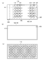
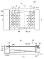
- the additional drive electrode 112 is provided to be positioned on the front or back of a part of the plurality of pairs according to the storage state of the display unit 102, and the additional capacitance 508 between the pair of detection electrodes 110 according to the storage state. (Described later) is formed. Specifically, this will be described with reference to FIG. FIG. 4A is a view of the display unit 102 as viewed from above, and FIG. 4B is a view of the display unit 102 as viewed from the back. As shown in FIG. 4A, the main drive electrodes 108 and the detection electrodes 110 are arranged on the front surface of the display unit 102 in the display area 128 for displaying an image.
- a fixed area 404, a drive circuit 122, and a connection portion 402 are provided outside the display area 128 on the surface of the display unit 102.
- the fixed area 404 is an area fixed to the winding unit 118. Details of the drive circuit 122 will be described later.
- the connection portion 402 is, for example, a conductive seal or the like, and electrically connects the front surface and the back surface of the display portion 102.
- the additional drive electrode 112 is disposed on the entire surface or in a lattice shape on the surface opposite to the surface on which the main drive electrode 108 and the detection electrode 110 of the display unit 102 are disposed. Specifically, for example, as shown in FIG. 4B, the additional drive electrode 112 is disposed without a gap over the entire back surface except for the peripheral portion of the display unit 102. Further, as shown in FIG. 4C, for example, the additional drive electrode 112 may have a lattice shape. The additional drive electrode 112 is shown in FIGS. 4B and 4C if it is disposed on the back surface corresponding to the position where the detection electrode 110 disposed on the surface and the additional capacitance 508 are formed. It does not have to be in shape.
- the additional drive electrode 112 is electrically connected to the surface of the display unit 102 via the connection unit 402 at the end of the display unit 102. Furthermore, the connection portion 402 on the front surface and the drive circuit 122 are connected by a wire (not shown). Thereby, the drive circuit 122 and the additional drive electrode 112 are electrically connected.
- the first storage unit 106 has a winding unit 118 in which the fixing unit 120 is provided.
- the first storage portion 106 is a metal or resin housing, and accommodates the winding portion 118 inside.
- the winding portion 118 has, for example, a cylindrical shape, and has a fixing portion 120.
- the fixing unit 120 is a partial area of the surface of the winding unit 118, and fixes the display unit 102 to the winding unit 118 by a seal, an adhesive, or the like.
- the winding unit 118 winds part or all of the display unit 102 such that the surface on which the main drive electrode 108 and the detection electrode 110 are disposed is inside.
- the storage unit stores a part or all of the display unit 102 inside the housing.
- FIG. 1B in the state where all the display unit 102 is pulled out from the first storage unit 106, the surface on the side where the main drive electrode 108 and the detection electrode 110 of the display unit 102 are arranged is wound. It is fixed to the part 118.
- the winding unit 118 winds up the display unit 102 by rotating clockwise in the drawing of FIG. 1 (b). As shown in FIG.
- the display unit 102 in the state where a part of the display unit 102 is wound up, a part of the display unit 102 including the display area 128 is wound up by the wind-up unit 118. Furthermore, as shown in FIG. 3B, in the state where all the display units 102 are stored in the first storage unit 106, the display unit 102 excludes most of the area except a part of the vicinity of the entrance of the first storage unit 106. Is taken up by the take-up unit 118.
- the shape of the winding portion 118 may not be cylindrical.
- the winding unit 118 may be a polygonal column or a rounded corner of the polygonal column.
- the second storage unit 116 has a fixing unit 120 inside.
- the second storage unit 116 is a case made of metal or resin, and accommodates the fixing unit 120 inside.
- the fixing unit 120 has, for example, a rectangular parallelepiped shape, and one surface is fixed to the inner wall of the second storage unit 116, and the other surface fixes the end of the display unit 102. Thereby, the positional relationship between the display unit 102 and the second storage unit 116 is fixed.
- the second storage unit 116 accommodates a part of the display unit 102 inside. Specifically, as shown in FIG. 1B, the second storage unit 116 internally accommodates the drive circuit 122, the control circuit 124, and the connection line 126.
- the drawer structure 114 is a mechanism that regulates the positional relationship between the first storage unit 106 and the second storage unit 116. Specifically, for example, as shown in FIG. 1B, the drawer structure 114 has a shape in which flat plates are connected in a step-like manner. When all the display units 102 are pulled out of the first storage unit 106, the drawer structure 114 is in the most stretched state. Thereby, the drawer structure 114 regulates the positional relationship between the first storage unit 106 and the second storage unit 116 so that the first storage unit 106 and the second storage unit 116 are not separated from each other by a predetermined distance.
- the drawer structure 114 expands and contracts. Specifically, for example, as shown in FIG. 2B, in the state where a part of the display unit 102 is stored in the first storage unit 106, the drawer structure 114 has a drawer structure shown in FIG. 1B. It is shrunk to about half the length of the body 114. Furthermore, as shown in FIG. 3B, in the state where all the display units 102 are stored in the first storage unit 106, the drawer structure 114 is the shortest, and is accommodated in the first storage unit 106. By expanding and contracting the drawer structure 114, the size of the displayed screen can be changed according to the size of the extracted region of the display device 100.
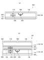
- FIG. 5A is a cross-sectional view of the display unit 102 in the extracted area.
- FIG. 5 (b) is a view showing a cross section of the display unit 102 in the wound area, and is a view showing the display unit 102 superimposed on the winding unit 118.
- the display unit 102 includes the display panel 500, the main drive electrode 108, the detection electrode 110, the surface protection film 504, the additional drive electrode 112, and the back surface protection film 502. Have.
- the display panel 500 is a thin panel that displays an image such as an organic EL panel, for example.
- the display panel 500 is provided with an array layer on which a TFT (Thin Film Transistor) and a capacitor are formed, an organic EL (Electro Luminescence) layer that emits light, and the like. Do.
- the main drive electrode 108 and the detection electrode 110 are disposed on one surface of the display unit 102. Specifically, the pair of the main drive electrode 108 and the detection electrode 110 is disposed close to the surface of the display panel 500 so that each becomes an electrode of a capacitor to form a main capacitance 506.
- the surface protective film 504 is disposed to cover the main drive electrode 108 and the detection electrode 110. Specifically, the surface protective film 504 is disposed to cover the main drive electrode 108 and the detection electrode 110 by a material such as SiN, and protects the main drive electrode 108 and the detection electrode 110.
- the additional drive electrode 112 is disposed on the back surface of the display panel 500. Specifically, the additional drive electrode 112 is disposed on the back surface of the display panel 500 so as to form an additional capacitance 508 between the display panel 500 and the detection electrode 110.
- the back surface protection film 502 is disposed to cover the additional drive electrode 112. Specifically, the back surface protective film 502 is disposed to cover the additional drive electrode 112 with a material such as SiN, and protects the additional drive electrode 112.
- An additional capacitance 508 is formed only between the detection electrode 110 of the display portion 102 in the extracted region and the additional drive electrode 112 disposed across the display panel 500.
- the detection electrode 110 is added to the additional drive electrode 112 disposed across the display panel 500, and the inner side for one turn.
- An additional capacitance 508 is formed between the additional drive electrode 112 disposed on the Specifically, the display unit 102 in the wound area is disposed in two layers. Since the additional drive electrode 112 arranged on the inner side and the detection electrode 110 arranged on the outer side of one turn are arranged close to each other, an additional capacitance 508 is formed between the both electrodes.
- the additional capacitance 508 formed on the detection electrode 110 disposed in the wound area is formed on the detection electrode 110 disposed in the drawn area. Is greater than the additional capacitance 508. As described later, the storage state is determined using the difference in magnitude of the capacitance.
- FIG. 6 is a functional block diagram of the display device 100.
- the display device 100 includes an external device 602, a control unit 604, a drive unit 606, a display panel unit 608, a sensor unit 610, a detection unit 612, and a determination unit 614.
- the functions of the control unit 604 and the determination unit 614 are realized by the operation of the control circuit 124 in FIG. 1 (b) to FIG. 3 (b).
- the functions of the drive unit 606 and the detection unit 612 are realized by the operation of the drive circuit 122 shown in FIGS. 1 (b) to 3 (b).
- the control unit in the claims corresponds to the control unit 604 and the determination unit 614 in FIG. Further, the upper side in the drawing of FIG. 6 corresponds to the left side in the drawing in FIG.
- the external device 602 is a device that transmits and receives video signals and data related to touched coordinates to the display device 100.
- the external device 602 is a PC (Personal Computer) or the like, transmits a video signal to the control unit 604, and acquires data on coordinates touched by the control unit 604.
- PC Personal Computer
- the control unit 604 controls the operation of the detection unit 612 and the drive unit 606. Specifically, the control unit 604 acquires an image signal and power from the external device 602. The control unit 604 generates an image signal, a signal for controlling the timing of lighting a pixel, and the like based on the acquired image signal and power supply, and supplies the signal to the display panel drive unit 616. The control unit 604 generates signals for operating or stopping each of the main drive electrode drive unit 618, the additional drive electrode drive unit 620, and the detection unit 612 based on the acquired image signal, and supplies the generated signals to the respective units.
- control unit 604 limits the detection operation of the detection unit 612 according to the storage state. Specifically, the control unit 604 stops the detection operation of the detection unit 612 with respect to the detection electrode 110 disposed in the area stored in the first storage unit 106. Details of the operation will be described later using a timing chart.
- the drive unit 606 includes a display panel drive unit 616, a main drive electrode drive unit 618, and an additional drive electrode drive unit 620.
- the display panel drive unit 616 generates a power supply and a signal to be supplied to the display panel 500. Specifically, the display panel drive unit 616 generates a power supply or a signal to be supplied to each pixel of the display panel unit 608 based on the image signal acquired from the control unit 604, and supplies the generated power or signal to the display panel unit 608.
- the display panel unit 608 displays an image by the power supply and the signal.
- the main drive electrode drive unit 618 supplies a main drive signal to the main drive electrode 108 to change the voltage of the detection electrode 110 via the main capacitance 506. Specifically, based on the signal acquired from the control unit 604, the main drive electrode drive unit 618 generates a main drive signal to be supplied to the main drive electrode 108.
- the main drive electrode drive unit 618 sequentially supplies main drive signals to the plurality of main drive electrodes 108 from right to left in FIG.
- the main drive signal is, for example, a pulse signal having a predetermined amplitude.
- the main drive electrode drive unit 618 supplies a main drive signal in a normal operation period 806 described later.
- the additional drive electrode driver 620 supplies an additional drive signal to the additional drive electrode 112 to change the voltage of the detection electrode 110 via the additional capacitance 508. Specifically, the additional drive electrode drive unit 620 generates an additional drive signal to be supplied to the additional drive electrode 112 based on the signal acquired from the control unit 604. The additional drive electrode driver 620 supplies an additional drive signal to the additional drive electrode 112.
- the additional drive signal is, for example, a pulse signal having a predetermined amplitude.
- the additional drive electrode drive unit 620 supplies an additional drive signal during a winding position determination period 810 described later.
- the display panel unit 608 displays an image based on the power supply and the signal acquired from the display panel drive unit 616.
- the function of the display panel unit 608 is realized by the display panel 500 of FIGS. 5 (a) and 5 (b).
- the sensor unit 610 supplies the detection unit 612 with a voltage according to the main drive signal acquired from the main drive electrode drive unit 618 and the state in which the user touches the touch panel 104. Specifically, for example, the sensor unit 610 obtains a pulse signal of a predetermined amplitude from the main drive electrode drive unit 618. The pulse signal fluctuates the voltage of the detection electrode 110 via the main capacitance 506 formed between the main drive electrode 108 and the detection electrode 110. The sensor unit 610 supplies the voltage of the detection electrode 110 to the detection unit 612. The function of the sensor unit 610 is realized by the main drive electrode 108 and the detection electrode 110 of FIGS. 5 (a) and 5 (b).
- the detection unit 612 detects the voltage of the detection electrode 110. Specifically, each time the main drive signal is input to each of the main drive electrodes 108, the detection unit 612 sequentially sets the voltages of the plurality of detection electrodes 110 in the scanning direction 130 shown in FIG. To detect. The detection unit 612 performs the detection in a normal operation period 806 and a winding position determination period 810, which will be described later.
- Determination unit 614 determines the coordinates at which the user has touched touch panel 104. Specifically, for the detection electrode 110 not touched by the user in the area extracted from the first storage unit 106, the capacitance (main electrostatic capacitance) is set between the main drive electrode 108 and the additional drive electrode 112. A capacitance 506 and an additional capacitance 508) are formed. On the other hand, for the detection electrode 110 touched by the user, in addition to the above-mentioned electrostatic capacitance, an electrostatic capacitance is formed between the user's finger and the detection electrode 110. Therefore, the voltage which changes with the main drive signal via the main capacitance 506 differs between the detection electrode 110 which the user touched, and the detection electrode 110 which is not touched.
- the main drive electrode driving unit 618 sequentially supplies the plurality of main drive electrodes 108 from the right to the left in FIG. 6. Further, each time a main drive signal is input to each of the main drive electrodes 108, the detection unit 612 sequentially detects voltages of the plurality of detection electrodes 110 arranged in the scanning direction 130 shown in FIG. The determination unit 614 determines the coordinates at which the user touches the touch panel 104 based on the position of the main drive electrode 108 to which the main drive signal is input and the position of the detection electrode 110 at which a voltage different from a predetermined voltage is detected. judge.
- the determination unit 614 determines the storage state based on the change in voltage of the detection electrode 110 due to the additional drive signal. For example, the determination unit 614 determines the storage state based on whether or not the change in voltage of the detection electrode 110 is larger than a predetermined value. Specifically, when the additional drive signal is input to the additional drive electrode 112, the voltage of the detection electrode 110 changes via the additional capacitance 508.
- the additional capacitance 508 formed for the detection electrode 110 in the wound region is the detection electrode 110 in the extracted region. The additional capacitance 508 formed for Therefore, when the additional drive signal is input to the additional drive electrode 112, the voltage of the detection electrode 110 in the wound region changes more than the voltage of the detection electrode 110 in the extracted region.
- FIG. 7A is a graph showing the voltage detected by the detection unit 612 when the additional drive signal is input to the additional drive electrode 112.
- the vertical axis in FIG. 7A is the voltage detected by the detection unit 612, and the horizontal axis is the coordinate in the scanning direction 130.
- detection voltage is different bordering on a specific coordinate.
- the determination unit 614 determines that the area of the display unit 102 corresponding to the coordinates at which a voltage larger than the predetermined voltage is detected in FIG. 7A is stored in the first storage unit 106.
- the determination unit 614 may determine the storage state based on the magnitude of the change in the storage direction of the voltage of the detection electrode 110.
- FIG. 7B is a graph showing data obtained by differentiating the relationship between the detected voltage and the coordinates shown in FIG. 7A in the scanning direction 130.
- the differentiated detection voltage has a peak at the coordinate at which the detection voltage changes.
- the determination unit 614 may determine that the area of the display unit 102 corresponding to coordinates larger than the peak coordinates is stored in the first storage unit 106.
- the position determined as the boundary between the area stored in the first storage unit 106 and the extracted area is referred to as a storage position.
- the display unit 102 has a region between the region wound up by the winding unit 118 and the entrance of the first storage unit 106. .
- the detection electrode 110 is not provided with the additional drive electrode 112 on the surface. Therefore, according to the above determination method, a voltage equal to the predetermined voltage is detected in the detection electrode 110 in the area.
- the area is not an area wound up by the winding unit 118 but is an area not pulled out from the first storage unit 106. Therefore, the determination unit 614 stores the size of the area in advance, and determines that the area obtained by adding the size stored in advance to the area determined above is stored in the first storage unit 106. You may
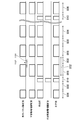
- FIG. 8 is a timing chart showing operations of the display panel drive unit 616, the main drive electrode drive unit 618, the detection unit 612, the additional drive electrode drive unit 620, and the determination unit 614.
- Every one frame period includes a normal operation period 806 and a stop period 808.
- the specific one frame period 802 inserted for each of a plurality of frames includes a winding position determination period 810.
- the normal operation period 806 is a period from the start timing of one frame to the timing when the display panel drive unit 616 scans the storage position.
- the stop period 808 is a period from the timing when the display panel drive unit 616 scans the storage position to the end timing of one frame.
- a partial period of the stop period 808 is replaced with the winding position determination period 810.
- the display panel drive unit 616 supplies power and image signals to each pixel of the display panel 500 during the normal operation period 806. Specifically, the display panel drive unit 616 supplies an image signal and power to the display panel 500 in the area drawn from the first storage unit 106. Further, the display panel drive unit 616 stops the supply of part of the power and the image signal to the display panel 500 in the area stored in the first storage unit 106.
- the main drive electrode driver 618 supplies a main drive signal to the main drive electrode 108 during the normal operation period 806. Specifically, the main drive electrode drive unit 618 sequentially supplies main drive signals to the plurality of main drive electrodes 108 from the right to the left in FIG. The main drive electrode driving unit 618 performs the operation once or a plurality of times until the normal operation period 806 ends.
- the detection unit 612 detects the voltage of the detection electrode 110 in the normal operation period 806 and the winding position determination period 810. Specifically, in the normal operation period 806, the detection unit 612 detects the voltage of the detection electrode 110 in the area extracted from the first storage unit 106. The detection unit 612 performs the operation once or a plurality of times until the normal operation period 806 ends. The detection unit 612 detects the voltage of the detection electrode 110 in the winding position determination period 810 in the frame including the winding position determination period 810.
- the additional drive electrode driving unit 620 supplies an additional drive signal to the additional drive electrode 112 during the winding position determination period 810. Specifically, the additional drive electrode driver 620 supplies the additional drive signal to the additional drive electrode 112 one or more times during the winding position determination period 810.
- Determination unit 614 determines the coordinates at which the user touches touch panel 104 during normal operation period 806. Further, the determination unit 614 determines the storage state in the winding position determination period 810. Specifically, determination unit 614 is based on the position of main drive electrode 108 to which the main drive signal is input during normal operation period 806 and the position of detection electrode 110 at which a voltage different from a predetermined voltage is detected. Then, the coordinates at which the user touches the touch panel 104 are determined. In addition, the determination unit 614 determines the storage position during the winding position determination period 810 based on the voltage detected by the detection unit 612 according to the determination method described using FIG. 7A or 7B. Do.
- the storage position is determined for each of a plurality of frames.
- the control unit 604 determines the lengths of the normal operation period 806 and the stop period 808 based on the determined latest storage position. Further, the control unit 604 controls the operations of the display panel drive unit 616, the main drive electrode drive unit 618, and the detection unit 612 described above. As a result, the display panel 500 and the touch panel 104 arranged in the area stored in the first storage unit 106 stop operating.
- FIG. 9 is a flowchart showing an operation performed by the display device 100. Note that FIG. 9 describes the timing at which the normal operation period 806 in a specific frame including the winding position determination period 810 in FIG. 8 ends as a starting point.
- the main drive electrode drive unit 618 stops the supply of the main drive signal to the main drive electrode 108 (S902).
- the display panel drive unit 616 also stops supply of an image signal or the like to the display panel 500 at the same timing.
- the additional drive electrode driving unit 620 supplies an additional drive signal to the additional drive electrode 112 (S904).
- the detection unit 612 detects a change in voltage of the detection electrode 110 according to the additional drive signal supplied in S904 (S906).
- control unit 604 determines the scanning range of the display panel 500 based on the determined storage position, and instructs the driving unit 606. Specifically, control unit 604 is a signal including information on normal operation period 806 and stop period 808 to display panel drive unit 616, main drive electrode drive unit 618, additional drive electrode drive unit 620 and detection unit 612. Supply.
- the additional drive electrode driving unit 620 stops the supply of the additional drive signal to the additional drive electrode 112 (S912). Steps S904 to S912 are performed in the winding position determination period 810.
- the display panel drive unit 616 resumes the supply of the image signal, the power source, and the like to the display panel 500 (S914).
- the display panel drive unit 616 supplies an image signal, a power source, and the like to the display panel 500 in the extracted area based on the signal related to the scanning range acquired in S910.
- the main drive electrode drive unit 618 resumes the supply of the main drive signal to the main drive electrode 108 (916).
- the detection unit 612 detects a change in voltage of the detection electrode 110 disposed in the extracted region (S918). The operations of S914 to S918 are performed simultaneously.
- the determination unit 614 determines the coordinates at which the user has touched the touch panel 104 based on the voltage detected in S918 (S920). After S920, when the normal operation period 806 ends, the display panel drive unit 616, the main drive electrode drive unit 618, and the detection unit 612 stop the operation during the stop period 808. In addition, the processing returns to step S914 at the timing when the stop period 808 ends and the normal period starts. Furthermore, the steps after S914 are repeated until the winding position determination period 810 is started.
- the display panel drive unit 616, the main drive electrode drive unit 618, and the detection unit 612 use the display panel 500 in the area stored in the first storage unit 106 based on the storage position updated every fixed period. And the operation of the touch panel 104 is stopped. As a result, power consumption and malfunction can be reduced by not performing unnecessary image display and determination of touched coordinates.
- the second embodiment differs from the first embodiment in the direction in which the winding unit 118 winds up the display unit 102 and the relationship between the storage position and the normal operation period 806.
- the other points are the same as in the first embodiment, and thus the description will be omitted.
- FIG. 10A and FIG. 10B are diagrams showing a mechanical configuration of the display device 100 according to the second embodiment.
- FIG. 10A is a plan view of the display device 100 as viewed from the top.
- FIG. 10 (b) is a view showing a cross section along line XX in FIG. 10 (a).
- Fig.10 (a) the top view seen from the upper surface of the display apparatus 100 is the same as that of 1st Embodiment.
- the winding unit 118 winds the display unit 102 such that the surface on which the main drive electrode 108 and the detection electrode 110 are disposed is on the outside.
- the surface on the side where the additional drive electrode 112 of the display unit 102 is disposed is fixed to the winding unit 118.
- the winding unit 118 winds up the display unit 102 by rotating counterclockwise in the drawing of FIG. 10B.
- An additional capacitance 508 is formed between the detection electrode 110 disposed on the outer side and the additional drive electrode 112 disposed on the outer side of one turn.
- the additional drive electrode 112 forming the detection electrode 110 and the additional capacitance 508 is not present outside the outermost detection electrode 110 of the display unit 102 taken up. Therefore, the additional capacitance 508 is not formed unless the display unit 102 is wound up for at least one turn.
- the control unit 604 controls the length of the normal driving period in consideration of the length of one turn of the winding unit 118. Specifically, the determination unit 614 determines the storage state based on the change in the voltage of the detection electrode 110 according to the additional drive signal, as in the first embodiment. The determination unit 614 determines the storage position by the method described in FIG. 7A or 7B. The determined storage position is a position shifted by one rotation from the position of the display unit actually stored. Therefore, the control unit 604 controls the normal driving period to be shorter by a scanning period corresponding to the length of one rotation of the winding shaft as compared with the first embodiment.
- FIG. 11 is a timing chart showing operations of the display panel drive unit 616, the main drive electrode drive unit 618, the detection unit 612, the additional drive electrode drive unit 620, and the determination unit 614.
- the timing at which the normal operation period 806 starts is simultaneous with the timing at which one frame starts.
- the timing at which the normal operation period 806 ends is a timing obtained by going back from the timing 1102 corresponding to the storage position determined by the determination unit 614 by a scanning period 1104 corresponding to the length of one turn of the winding axis.
- the period from the end of the normal operation period 806 to the end of the one frame period 802 is the stop period 808.
- one frame period 802 including the winding position determination period 810 is inserted every plural frames.
- the determination unit 614 stores the size of the region between the region wound up by the winding unit 118 and the entrance of the first storage unit 106 in advance. It may be determined that the area obtained by adding the size stored in advance to the determined area is stored in the first storage unit 106.
- the third embodiment differs from the first and second embodiments in that the additional drive electrode 112 is provided outside the display unit 102.
- the description of the same configuration as the other first and second embodiments will be omitted.
- FIG. 12A and FIG. 12B are diagrams showing a mechanical configuration of the display device 100 according to the second embodiment.
- FIG. 12A is a plan view of the display device 100 as viewed from the top.
- FIG. 12 (b) is a view showing a cross section taken along line XII-XII of FIG. 12 (a).
- a plan view seen from the top of the display device 100 is the same as in the first and second embodiments.
- the display device 100 further includes a roll pair 1202 disposed in the vicinity of the entrance with the display unit 102 interposed therebetween. Specifically, the display device 100 has a roll pair 1202 disposed near the entrance of the first storage unit 106 with the display unit 102 interposed therebetween. The roll pair 1202 is disposed inside the first storage unit 106. The roll pair 1202 reduces the sliding friction that occurs when the display unit 102 is taken up by the take-up unit 118.
- the additional drive electrode 112 is disposed near the entrance where the display unit 102 is stored. Specifically, one of the pair of rolls 1202 disposed near the entrance for storing the display unit 102 is the additional drive electrode 112. Of the two rolls of the roll pair 1202, the roll on the side where the detection electrode 110 of the display unit 102 is disposed may be the additional drive electrode 112, and the opposite roll may be the additional drive electrode 112. .
- the roll which is the additional drive electrode 112 is formed of a conductive material, and an additional drive signal is input.
- a circuit having the function of the additional drive electrode drive unit 620 is disposed inside the first storage unit 106. The circuit having the function of the additional drive electrode drive unit 620 supplies an additional drive signal to one of the roll pair 1202.
- the additional drive electrode 112 is not disposed on the back surface of the display panel 500.
- the determination unit 614 determines the storage state based on the change in voltage of the detection electrode 110 due to the additional drive signal. Specifically, one of the roll pair 1202 which is the additional drive electrode 112 and the detection electrode 110 are disposed close to each other. Therefore, an additional capacitance 508 is formed between one of the roll pair 1202 which is the additional drive electrode 112 and the detection electrode 110.
- the detection unit 612 detects a voltage of a large value only at a specific coordinate.
- the determination unit 614 determines the coordinates at the peak of the detection result of the detection unit 612 as the storage position.
- the power consumption and the malfunction can be reduced by determining the storage position and not performing the unnecessary image display and the determination of the touched coordinates.
- the additional drive electrode 112 may have another shape.
- the additional drive electrode 112 is a single rectangular conductor, and an additional capacitance 508 is formed in the vicinity of the entrance of the first storage portion 106 with the detection electrode 110. It may be located at
- the display device 100 has a configuration capable of storing the display unit 102.
- the configuration may have no winding shaft.
- the first storage unit 106 may be configured to have a space for storing the entire display unit 102 while the shape of the display unit 102 is constant. In this case, the display unit 102 is stored in the first storage unit 106 by sliding. Further, the first storage unit 106 may be configured to have a mechanism for folding the display unit 102 in a bellows shape and storing the same.
Landscapes
- Engineering & Computer Science (AREA)
- Theoretical Computer Science (AREA)
- Physics & Mathematics (AREA)
- General Physics & Mathematics (AREA)
- General Engineering & Computer Science (AREA)
- Human Computer Interaction (AREA)
- Devices For Indicating Variable Information By Combining Individual Elements (AREA)
- Electroluminescent Light Sources (AREA)
- Control Of Indicators Other Than Cathode Ray Tubes (AREA)
Abstract
タッチパネルの状態を検出するための専用の検出電極が不要であり、構成が簡略で小型な表示装置を提供する。 タッチパネルが設けられた表示部と、格納部と、を有する表示装置であって、格納部は表示部を格納し、タッチパネルは主駆動電極及び検出電極の複数のペアと、検出電極の電圧を検出する検出部と、主駆動信号を主駆動電極に供給する駆動部と、検出部及び駆動部の動作を制御する制御部と、を有し、表示装置は、さらに、ペアの一部の表または裏に配置され、表示部の格納状態に応じて検出電極との間に付加静電容量が形成される付加駆動電極を有し、駆動部は、さらに、付加静電容量を介して検出電極の電圧を変化させる付加駆動信号を付加駆動電極に供給し、制御部は、さらに、付加駆動信号による検出電極の電圧の変化に基づいて格納状態を判別するとともに、格納状態に応じて検出部の検出動作を制限する、ことを特徴とする。
Description
本発明は、表示装置に関する。
近年、コンパクトに収納可能なフレキシブルな表示装置の研究開発が進められている。また、近年、タッチパネルを備えた多くの表示装置が実用化されている。フレキシブル表示装置の消費電力を低減するために、タッチパネルの状態に応じて、タッチパネルの機能の一部を停止する機能を有する表示装置が知られている。例えば下記特許文献1は、タッチパネルを備えた表示部の一部または全部を巻き取る巻き取り部と、巻き取られた領域を検出する検出部と、を有し、タッチパネルの巻き取られた領域の動作を停止させる表示装置を開示している。
タッチパネルの状態に応じて、タッチパネルの機能の一部を停止するためには、タッチパネルの状態を検出する必要がある。例えば上記特許文献1は、巻き取られた領域を検出する為に、専用の検出部が設けられている。しかしながら、専用の検出部を設けると、画像表示装置内部の構造が複雑になる。
本発明は上記課題に鑑みてなされたものであって、その目的は、タッチパネルの状態を検出するための専用の検出電極が不要であり、構成が簡略で小型な表示装置を提供することにある。
本発明の一態様は、タッチパネルが設けられた表示部と、格納部と、を有する表示装置であって、前記格納部は、前記表示部の一部または全部を格納し、前記タッチパネルは、前記格納する方向に離間して配置され、相互に主静電容量を形成する主駆動電極及び検出電極の複数のペアと、前記検出電極の電圧を検出する検出部と、前記主静電容量を介して前記検出電極の電圧を変化させる主駆動信号を前記主駆動電極に供給する駆動部と、前記検出部及び前記駆動部の動作を制御する制御部と、を有し、前記表示装置は、さらに、前記複数のペアのうち前記表示部の格納状態に応じた一部の表または裏に位置するよう設けられ、前記格納状態に応じて前記検出電極との間に付加静電容量が形成される付加駆動電極を有し、前記駆動部は、さらに、前記付加静電容量を介して前記検出電極の電圧を変化させる付加駆動信号を前記付加駆動電極に供給し、前記制御部は、さらに、前記付加駆動信号による前記検出電極の電圧の変化に基づいて前記格納状態を判別するとともに、前記格納状態に応じて前記検出部の検出動作を制限する、ことを特徴とする。
以下に、本発明の各実施の形態について、図面を参照しつつ説明する。なお、開示はあくまで一例に過ぎず、当業者において、発明の主旨を保っての適宜変更について容易に想到し得るものについては、当然に本発明の範囲に含有されるものである。また、図面は、説明をより明確にするため、実際の態様に比べ、各部の幅、厚さ、形状等について模式的に表される場合があるが、あくまで一例であって、本発明の解釈を限定するものではない。また、本明細書と各図において、既出の図に関して前述したものと同様の要素には、同一の符号を付して詳細な説明を適宜省略することがある。
また、下記の各実施形態においては、開示例として有機EL表示装置の場合を例示したが、その他の適用例として、液晶表示装置、その他の自発光型表示装置、あるいは電気泳動素子等を有する電子ペーパー型表示装置等あらゆるフラットパネル型の表示装置が挙げられる。また、中小型から大型まで、特に限定することなく適用が可能であることは言うまでもない。
[第1の実施形態]
まず、第1の実施形態に係る表示装置100の機械的な構成について説明する。図1(a)、図1(b)、図2(a)、図2(b)、図3(a)及び図3(b)は、いずれも第1の実施形態に係る表示装置100の概略を示す図である。図1(a)、図2(a)、図3(a)は、表示装置100の上面から見た平面図である。図1(b)は、図1(a)のI-I断面を示す図である。図2(b)は図2(a)のII-II断面を示す図である。図3(b)は図3(a)のIII-III断面を示す図である。
まず、第1の実施形態に係る表示装置100の機械的な構成について説明する。図1(a)、図1(b)、図2(a)、図2(b)、図3(a)及び図3(b)は、いずれも第1の実施形態に係る表示装置100の概略を示す図である。図1(a)、図2(a)、図3(a)は、表示装置100の上面から見た平面図である。図1(b)は、図1(a)のI-I断面を示す図である。図2(b)は図2(a)のII-II断面を示す図である。図3(b)は図3(a)のIII-III断面を示す図である。
また、図1(a)及び図1(b)は、表示部102を第1格納部106から全て引き出した状態を示す図である。図2(a)及び図2(b)は、表示部102を第1格納部106から一部を引き出した状態を示す図である。図3(a)及び図3(b)は、表示部102を全て第1格納部106に格納した状態を示す図である。
図1(a)及び(b)に示すように、表示装置100は、タッチパネル104が設けられた表示部102と、第1格納部106と、第2格納部116と、引き出し構造体114と、を有する。表示部102は、表示領域128と、表示領域128の外側に配置された駆動回路122、制御回路124及び接続線126を有する。
表示領域128は、それぞれ複数の副画素で構成された複数の画素がマトリクス状に配置される。表示領域128には、各画素が発光することにより画像を表示する。
駆動回路122は、各画素に供給する電源や信号を生成する。具体的には、駆動回路122は、各画素に供給する電源や信号を生成するICであって、例えば、各副画素に配置された駆動トランジスタに対してソース・ドレイン間を導通させるための電位を印加すると共に、各データ信号線に対して階調値に対応する電流を流す。駆動回路122によって、表示部102は、表示領域128に画像を表示する。
制御回路124は、駆動回路122の動作を制御する。接続線126は、導電性を有する材料で形成され、駆動回路122と制御回路124を電気的に接続する。なお、駆動回路122及び制御回路124の機能については後で詳述する。
また、タッチパネル104及び表示部102は、可撓性を有する。具体的には、表示部102は、第1格納部106と第2格納部116の間に配置され、第2格納部116から第1格納部106へ向かう方向(図面上右から左へ向かう方向、以下格納する方向とする)に向かって、第1格納部106に格納される。後述するように第1格納部106は巻き取り部118を有し、タッチパネル104及び表示部102は、格納された状態で巻き取り部118の周りに巻きつけられるように可撓性を有する。
タッチパネル104は、主駆動電極108及び検出電極110の複数のペアと、付加駆動電極112と、制御部604と、駆動部606と、検出部612と、を有する。制御部604、駆動部606及び検出部612については、図6を用いて説明する。
主駆動電極108及び検出電極110の複数のペアは、格納する方向に離間して配置され、相互に主静電容量506を形成する。具体的には、例えば、主駆動電極108は、格納する方向及び格納する方向と直交する方向に並べて配置された複数の菱形状の電極である。また、格納する方向に並べて配置された複数の主駆動電極108は、各菱形状の部分を接続する配線によって、それぞれ電気的に接続される。一方、格納する方向と直交する方向に並べて配置された複数の主駆動電極108は、電気的に接続されない。
検出電極110は、格納する方向及び格納する方向と直交する方向に並べて配置された複数の菱形状の電極である。また、格納する方向に並べて配置された複数の検出電極110は、それぞれ電気的に接続されない。一方、格納する方向と直交する方向に並べて配置された複数の検出電極110は、各菱形状の部分を接続する配線によって、電気的に接続される。なお、主駆動電極108及び検出電極110の形状はいずれも菱形以外の形状であってもよい。
また、格納する方向に並べて配置された複数の主駆動電極108を接続する配線と、格納する方向と直交する方向に並べて配置された複数の検出電極110を接続する配線と、は異なる層に形成される。これにより、主駆動電極108と検出電極110とは電気的に接続しないように形成される。さらに、主駆動電極108と、隣接する検出電極110と、は後述する主静電容量506を形成する。
付加駆動電極112は、複数のペアのうち表示部102の格納状態に応じた一部の表または裏に位置するよう設けられ、格納状態に応じて検出電極110との間に付加静電容量508(後述)が形成される。具体的には、図4を用いて説明する。図4(a)は、表示部102を上面から見た図であり、図4(b)は表示部102を裏面から見た図である。図4(a)に示すように、主駆動電極108及び検出電極110は、画像を表示する表示領域128において、表示部102の表に配置される。
表示部102の表面の表示領域128の外側には、固定領域404並びに駆動回路122及び接続部402が設けられる。固定領域404は、巻き取り部118と固定される領域である。駆動回路122の詳細は後述する。接続部402は、例えば、導電性を有するシール等であって、表示部102の表面と裏面を電気的に接続する。
付加駆動電極112は、表示部102の主駆動電極108及び検出電極110が配置された面の反対の面に、全面または格子状の形状に配置される。具体的には、例えば図4(b)に示すように、付加駆動電極112は、表示部102の周辺部を除いて裏面全体にわたって隙間なく配置される。また、例えば図4(c)に示すように、付加駆動電極112は、格子状であってもよい。なお、付加駆動電極112は、表面に配置された検出電極110と付加静電容量508が形成される位置に対応して裏面に配置されていれば、図4(b)及び(c)に示す形状でなくてもよい。
付加駆動電極112は、表示部102の端部において、接続部402を介して表示部102の表面と電気的に接続される。さらに、表面の接続部402と駆動回路122とは配線(図示なし)によって接続される。これにより、駆動回路122と付加駆動電極112とは電気的に接続される。
第1格納部106は、内部に固定部120が設けられた巻き取り部118を有する。具体的には、図1(b)に示すように、第1格納部106は、金属製または樹脂製の筐体であって、内部に巻き取り部118を収容する。巻き取り部118は、例えば円柱状の形状であって、固定部120を有する。固定部120は、巻き取り部118の表面の一部の領域であって、シールまたは接着剤等によって表示部102を巻き取り部118に固定する。
巻き取り部118は、主駆動電極108及び検出電極110が配置された面が内側になるように表示部102の一部または全部を巻き取る。これにより、格納部は、表示部102の一部または全部を筐体の内部に格納する。図1(b)に示すように、表示部102が全て第1格納部106から引き出された状態では、表示部102の主駆動電極108及び検出電極110が配置された側の面が、巻き取り部118に固定される。巻き取り部118は、図1(b)の図面上時計回りに回転することによって、表示部102を巻き取る。図2(b)に示すように、表示部102の一部が巻き取られた状態では、表示部102は、表示領域128を含む一部の領域が巻き取り部118に巻き取られる。さらに、図3(b)に示すように、表示部102を全て第1格納部106に格納した状態では、表示部102は、第1格納部106の入口近傍の一部の領域を除く大部分が巻き取り部118に巻き取られる。
なお、巻き取り部118の形状は、円柱状でなくてもよい。例えば、巻き取り部118は、多角柱でもよいし、多角柱の角を丸めた形状であってもよい。
第2格納部116は、内部に固定部120を有する。具体的には、第2格納部116は、金属製または樹脂製の筐体であって、内部に固定部120を収容する。固定部120は、例えば直方体の形状であって、一の面が第2格納部116の内壁に固定され、他の面は表示部102の端部を固定する。これにより、表示部102と第2格納部116の位置関係を固定する。
また、第2格納部116は、表示部102の一部を内部に収容する。具体的には、図1(b)に示すように、第2格納部116は、駆動回路122と、制御回路124と、接続線126と、を内部に収容する。
引き出し構造体114は、第1格納部106と、第2格納部116と、の位置関係を規制する機構である。具体的には、例えば図1(b)に示すように、引き出し構造体114は、平板が階段状に接続された形状である。表示部102が全て第1格納部106から引き出された状態で、引き出し構造体114は、最も引き伸ばされた状態となる。これにより、引き出し構造体114は、第1格納部106と第2格納部116が所定の距離より離れないように、第1格納部106と第2格納部116の位置関係を規制する。
また、引き出し構造体114は、伸縮する。具体的には、例えば図2(b)に示すように、表示部102の一部が第1格納部106に格納された状態では、引き出し構造体114は、図1(b)に示す引き出し構造体114の長さの半分程度に縮められる。さらに、図3(b)に示すように、表示部102を全て第1格納部106に格納した状態では、引き出し構造体114は、最も短くなり、第1格納部106の内部に収容される。引き出し構造体114が伸縮することにより、表示装置100の引き出された領域の大きさに応じて表示される画面の大きさを変えることが出来る。
続いて、表示部102の断面構成について説明する。図5(a)は、引き出された領域の表示部102の断面を示す図である。図5(b)は、巻き取られた領域にある表示部102の断面を示す図であって、巻き取り部118の上に重ねられた表示部102を示す図である。
図5(a)に示すように、表示部102は、表示パネル500と、主駆動電極108と、検出電極110と、表面保護膜504と、付加駆動電極112と、裏面保護膜502と、を有する。
表示パネル500は、例えば有機ELパネルなどの画像を表示する薄型のパネルである。表示パネル500は、TFT(Thin Film Transistor)やコンデンサが形成されたアレイ層や、光を発する有機EL(Electro Luminescence)層等が設けられるが、従来技術と同様であるため、詳細な説明は省略する。
主駆動電極108及び検出電極110は、表示部102の片側の面に配置される。具体的には、主駆動電極108と検出電極110のペアは、それぞれがコンデンサの電極となって主静電容量506を形成するように、表示パネル500の表面に近接して配置される。
表面保護膜504は、主駆動電極108及び検出電極110を覆うように配置される。具体的には、表面保護膜504は、SiNなどの材料によって主駆動電極108及び検出電極110を覆うように配置され、主駆動電極108及び検出電極110を保護する。
付加駆動電極112は、表示パネル500の裏面に配置される。具体的には、付加駆動電極112は、表示パネル500を挟んで検出電極110との間に付加静電容量508を形成するように、表示パネル500の裏面に配置される。
裏面保護膜502は、付加駆動電極112を覆うように配置される。具体的には、裏面保護膜502は、SiNなどの材料によって付加駆動電極112を覆うように配置され、付加駆動電極112を保護する。
引き出された領域にある表示部102の検出電極110は、表示パネル500を挟んで配置された付加駆動電極112との間にのみ付加静電容量508が形成される。一方、図5(b)に示すように、巻き取り部118に巻き取られた領域では、検出電極110は、表示パネル500を挟んで配置された付加駆動電極112に加えて、1周分内側に配置された付加駆動電極112との間に付加静電容量508を形成する。具体的には、巻き取られた領域にある表示部102は、2層重ねて配置される。内側に配置された付加駆動電極112と、1周外側に配置された検出電極110と、は近接して配置されるため、両電極間に付加静電容量508が形成される。
以上のように、巻き取られた領域に配置されている検出電極110に対して形成されている付加静電容量508は、引き出された領域に配置されている検出電極110に対して形成されている付加静電容量508よりも大きい。後述するように、当該静電容量の大きさの差を用いて、格納状態が判断される。
続いて、第1の実施形態に係る表示装置100の機能的な構成について説明する。図6は、表示装置100の機能的なブロック図である。表示装置100は、外部装置602と、制御部604と、駆動部606と、表示パネル部608と、センサ部610と、検出部612と、判定部614と、を有する。なお、制御部604及び判定部614の機能は、図1(b)乃至図3(b)の制御回路124の動作によって実現される。駆動部606及び検出部612の機能は、図1(b)乃至図3(b)の駆動回路122の動作によって実現される。また、特許請求の範囲における制御部は、図6の制御部604及び判定部614に相当する。さらに、図6の図面上上側が、図1(a)における図面上左側に相当する。
外部装置602は、表示装置100に対して、映像信号やタッチされた座標に関するデータの送受信をする装置である。具体的には、外部装置602は、PC(Personal Computer)等であって、制御部604に対して映像信号を送信し、制御部604からタッチされた座標に関するデータを取得する。
制御部604は、検出部612及び駆動部606の動作を制御する。具体的には、制御部604は、外部装置602から画像信号及び電源を取得する。制御部604は、取得した画像信号及び電源に基づいて、画像信号や画素を点灯させるタイミングを制御する信号等を生成し、表示パネル駆動部616に供給する。制御部604は、取得した画像信号に基づいて、主駆動電極駆動部618、付加駆動電極駆動部620及び検出部612のそれぞれを動作または停止させる信号等を生成し、各部に供給する。
また、制御部604は、格納状態に応じて検出部612の検出動作を制限する。具体的には、制御部604は、第1格納部106に格納された領域に配置された検出電極110に対する検出部612の検出動作を停止させる。当該動作の詳細については、タイミングチャートを用いて後述する。
駆動部606は、表示パネル駆動部616と、主駆動電極駆動部618と、付加駆動電極駆動部620と、有する。表示パネル駆動部616は、表示パネル500に対して供給する電源や信号を生成する。具体的には、表示パネル駆動部616は、制御部604から取得した画像信号に基づいて、表示パネル部608の各画素に供給する電源や信号を生成し、表示パネル部608に供給する。当該電源及び信号によって、表示パネル部608は、画像を表示する。
主駆動電極駆動部618は、主静電容量506を介して検出電極110の電圧を変化させる主駆動信号を主駆動電極108に供給する。具体的には、主駆動電極駆動部618は、制御部604から取得した信号に基づいて、主駆動電極108に対して供給する主駆動信号を生成する。主駆動電極駆動部618は、複数の主駆動電極108に対して、主駆動信号を図6の右から左に向かって順に供給する。主駆動信号は、例えば、所定の振幅を有するパルス信号である。なお、主駆動電極駆動部618は、後述する通常動作期間806に主駆動信号を供給する。
付加駆動電極駆動部620は、付加静電容量508を介して検出電極110の電圧を変化させる付加駆動信号を付加駆動電極112に供給する。具体的には、付加駆動電極駆動部620は、制御部604から取得した信号に基づいて、付加駆動電極112に対して供給する付加駆動信号を生成する。付加駆動電極駆動部620は、付加駆動信号を付加駆動電極112に供給する。付加駆動信号は、例えば、所定の振幅を有するパルス信号である。なお、付加駆動電極駆動部620は、後述する巻き取り位置判定期間810に、付加駆動信号を供給する。
表示パネル部608は、表示パネル駆動部616から取得した電源や信号に基づいて画像を表示する。表示パネル部608の機能は、図5(a)及び(b)の表示パネル500によって実現される。
センサ部610は、主駆動電極駆動部618から取得した主駆動信号と、タッチパネル104にユーザーが触れている状態と、に応じた電圧を検出部612に供給する。具体的には、例えば、センサ部610は、主駆動電極駆動部618から所定の振幅のパルス信号を取得する。当該パルス信号は、主駆動電極108と検出電極110と、の間に形成された主静電容量506を介して検出電極110の電圧を変動させる。センサ部610は、検出電極110の電圧を検出部612に供給する。センサ部610の機能は、図5(a)及び(b)の主駆動電極108及び検出電極110によって実現される。
検出部612は、検出電極110の電圧を検出する。具体的には、検出部612は、各主駆動電極108に主駆動信号が入力される毎に、複数配置された検出電極110の電圧を、図6に示す走査方向130に向かって順にまたは一度に検出する。検出部612は、後述する通常動作期間806及び巻き取り位置判定期間810に、当該検出を行う。
判定部614は、ユーザーがタッチパネル104に触れた座標を判定する。具体的には、第1格納部106から引き出された領域におけるユーザーが触れていない検出電極110に対しては、主駆動電極108と付加駆動電極112との間にのみ静電容量(主静電容量506及び付加静電容量508)が形成される。一方、ユーザーが触れた検出電極110に対しては、上記静電容量に加えて、ユーザーの指と検出電極110との間に静電容量が形成される。従って、ユーザーが触れた検出電極110と、触れていない検出電極110とでは、主静電容量506を介して主駆動信号によって変化する電圧が異なる。
ここで、上記のように、主駆動電極駆動部618は、複数の主駆動電極108に対して、図6の右から左に向かって順に供給する。また、検出部612は、各主駆動電極108に主駆動信号が入力される毎に、複数配置された検出電極110の電圧を、図6に示す走査方向130に向かって順に検出する。判定部614は、主駆動信号が入力された主駆動電極108の位置と、所定の電圧と異なる電圧が検出された検出電極110の位置と、に基づいて、ユーザーがタッチパネル104に触れた座標を判定する。
また、判定部614は、付加駆動信号による検出電極110の電圧の変化に基づいて格納状態を判別する。例えば、判定部614は、検出電極110の電圧の変化が所定の値より大きいか否かに基づいて格納状態を判別する。具体的には、付加駆動電極112に付加駆動信号が入力されると、検出電極110の電圧は、付加静電容量508を介して変化する。ここで、図5(a)及び(b)を用いて説明したように、巻き取られた領域の検出電極110に対して形成された付加静電容量508は、引き出された領域の検出電極110に対して形成された付加静電容量508よりも大きい。従って、付加駆動電極112に付加駆動信号が入力された場合に、巻き取られた領域の検出電極110の電圧は、引き出された領域の検出電極110の電圧よりも大きく変化する。
図7(a)は、付加駆動電極112に付加駆動信号が入力された場合に、検出部612が検出した電圧を示すグラフである。図7(a)の縦軸は検出部612が検出した電圧であり、横軸は走査方向130の座標である。図7(a)に示すように、特定の座標を境界として、検出電圧が異なっている。判定部614は、図7(a)において、所定の電圧よりも大きい電圧が検出された座標と対応する表示部102の領域が、第1格納部106に格納されていると判定する。
また、例えば、判定部614は、検出電極110の電圧の格納する方向に対する変化の大きさに基づいて、格納状態を判別してもよい。具体的には、図7(b)は、図7(a)に示す検出電圧と座標の関係を、走査方向130に微分したデータを示すグラフである。図7(b)に示すように、検出電圧が変化する座標において、微分された検出電圧はピークを有する。判定部614は、当該ピーク座標より大きい座標と対応する表示部102の領域が、第1格納部106に格納されていると判定してもよい。以下、当該第1格納部106に格納された領域と引き出された領域の境界として判定された位置を格納位置とする。
なお、図1(b)乃至図3(b)に示すように、表示部102は、巻き取り部118に巻き取られた領域と、第1格納部106の入り口と、の間の領域を有する。当該領域において、検出電極110は、表面に付加駆動電極112が配置されていない。従って、上記判定方法によれば、当該領域の検出電極110において、所定の電圧と同等の電圧が検出される。当該領域は、巻き取り部118に巻き取られた領域ではないものの、第1格納部106から引き出されていない領域である。従って、判定部614は、予め当該領域の大きさを記憶しておき、上記判定した領域に、予め記憶した大きさを加えた領域が、第1格納部106に格納されていると判定するようにしてもよい。
続いて、表示装置100の動作について、タイミングチャートを用いて説明する。図8は、表示パネル駆動部616、主駆動電極駆動部618、検出部612、付加駆動電極駆動部620及び判定部614の動作を示すタイミングチャートである。
全ての1フレームの期間は、通常動作期間806と、停止期間808と、を含む。また、複数フレーム毎に挿入される特定の1フレーム期間802は、通常動作期間806と、停止期間808とに加えて、巻き取り位置判定期間810を含む。具体的には、通常動作期間806は、1フレームの開始タイミングから、表示パネル駆動部616が格納位置を走査するタイミングまでの期間である。停止期間808は、表示パネル駆動部616が格納位置を走査するタイミングから、1フレームの終了タイミングまでの期間である。巻き取り位置判定期間810を含むフレームにおいては、停止期間808の一部期間が、巻き取り位置判定期間810に置き換えられる。
図8に示すように、表示パネル駆動部616は、通常動作期間806に表示パネル500の各画素に電源や画像信号を供給する。具体的には、表示パネル駆動部616は、第1格納部106から引き出された領域にある表示パネル500に対して、画像信号や電源を供給する。また、表示パネル駆動部616は、第1格納部106に格納された領域にある表示パネル500に対して、電源の一部及び画像信号の供給を停止する。
主駆動電極駆動部618は、通常動作期間806に主駆動電極108に主駆動信号を供給する。具体的には、主駆動電極駆動部618は、複数の主駆動電極108に対して、主駆動信号を図6の右から左に向かって順に供給する。主駆動電極駆動部618は、通常動作期間806が終了するまで1回または複数回当該動作を行う。
検出部612は、通常動作期間806及び巻き取り位置判定期間810に、検出電極110の電圧を検出する。具体的には、検出部612は、通常動作期間806において、第1格納部106から引き出された領域にある検出電極110の電圧を検出する。検出部612は、通常動作期間806が終了するまで当該動作を1回または複数回行う。また、検出部612は、巻き取り位置判定期間810を含むフレームにおいては、巻き取り位置判定期間810に、検出電極110の電圧を検出する。
付加駆動電極駆動部620は、巻き取り位置判定期間810に、付加駆動信号を付加駆動電極112に供給する。具体的には、付加駆動電極駆動部620は、巻き取り位置判定期間810に1回または複数回、付加駆動信号を付加駆動電極112に供給する。
判定部614は、通常動作期間806に、ユーザーがタッチパネル104に触れた座標を判定する。また、判定部614は、巻き取り位置判定期間810に格納状態を判別する。具体的には、判定部614は、通常動作期間806に、主駆動信号が入力された主駆動電極108の位置と、所定の電圧と異なる電圧が検出された検出電極110の位置と、に基づいて、ユーザーがタッチパネル104に触れた座標を判定する。また、判定部614は、巻き取り位置判定期間810に、検出部612が検出した電圧に基づいて、図7(a)または図7(b)を用いて説明した判定方法により、格納位置を判定する。
格納位置は、複数フレーム毎に判定される。制御部604は、判定された直近の格納位置に基づいて、通常動作期間806及び停止期間808の長さを決定する。また、制御部604は、上記の表示パネル駆動部616、主駆動電極駆動部618、検出部612の動作を制御する。これにより、第1格納部106に格納された領域に配置された表示パネル500及びタッチパネル104は、動作を停止する。
続いて、表示装置100の動作について、フローチャートを用いて説明する。図9は、表示装置100が行う動作を示すフローチャートである。なお、図9は、図8の巻き取り位置判定期間810を含む特定のフレームにおける通常動作期間806が終了したタイミングを起点として記載している。
通常動作期間806が終了したタイミングで、主駆動電極駆動部618は、主駆動電極108への主駆動信号の供給を停止する(S902)。なお、同じタイミングで、表示パネル駆動部616も、表示パネル500への画像信号等の供給を停止する。次に、付加駆動電極駆動部620は、付加駆動電極112に対して、付加駆動信号を供給する(S904)。次に、検出部612は、S904で供給された付加駆動信号による検出電極110の電圧の変化を検出する(S906)。
次に、判定部614は、S906で検出された電圧に基づいて、格納位置を判定する(S908)。制御部604は、判定された格納位置に基づいて、表示パネル500の走査範囲を決定し、駆動部606に指示を行う。具体的には、制御部604は、表示パネル駆動部616、主駆動電極駆動部618、付加駆動電極駆動部620及び検出部612に対して、通常動作期間806及び停止期間808に関する情報を含む信号を供給する。
次に、付加駆動電極駆動部620は、付加駆動電極112への付加駆動信号の供給を停止する(S912)。S904乃至S912までのステップは、巻き取り位置判定期間810に行われる。
次に、表示パネル駆動部616は、画像信号及び電源等の表示パネル500への供給を再開する(S914)。ここで、表示パネル駆動部616は、S910で取得した走査範囲に関する信号に基づいて、引き出された領域にある表示パネル500に対して、画像信号及び電源等を供給する。また、主駆動電極駆動部618は、主駆動電極108への主駆動信号の供給を再開する(916)。さらに、検出部612は、引き出された領域に配置された検出電極110の電圧の変化を検出する(S918)。S914乃至S918の動作は、同時に行われる。
次に、判定部614は、S918で検出された電圧に基づいて、ユーザーがタッチパネル104に触れた座標を判定する(S920)。S920の後、通常動作期間806が終了すると、停止期間808の間、表示パネル駆動部616、主駆動電極駆動部618及び検出部612は、動作を停止する。また、停止期間808が終了し通常期間が開始するタイミングでS914に戻る。さらに、巻き取り位置判定期間810が開始されるまで、S914以降のステップが繰り返される。
以上の動作により、表示パネル駆動部616、主駆動電極駆動部618、検出部612は、一定期間ごとに更新される格納位置に基づいて、第1格納部106に格納された領域における表示パネル500及びタッチパネル104の動作を停止する。これにより、不要な画像表示やタッチされた座標の判定を行わないことにより、消費電力及び誤動作を低減することができる。
[第2の実施形態]
続いて、第2の実施形態について説明する。第2の実施形態は、巻き取り部118が表示部102を巻き取る方向及び格納位置と通常動作期間806の関係が第1の実施形態と異なる。その他の点については、第1の実施形態と同様であるため、説明を省略する。
続いて、第2の実施形態について説明する。第2の実施形態は、巻き取り部118が表示部102を巻き取る方向及び格納位置と通常動作期間806の関係が第1の実施形態と異なる。その他の点については、第1の実施形態と同様であるため、説明を省略する。
図10(a)及び図10(b)は、第2の実施形態に係る表示装置100の機械的な構成を示す図である。図10(a)は、表示装置100の上面から見た平面図である。図10(b)は、図10(a)のX-X断面を示す図である。図10(a)に示すように、表示装置100の上面から見た平面図は、第1の実施形態と同様である。
第2の実施形態においては、巻き取り部118は、主駆動電極108及び検出電極110が配置された面が外側になるように表示部102を巻き取る。具体的には、図10(b)に示すように、表示部102の付加駆動電極112が配置された側の面が、巻き取り部118に固定される。巻き取り部118は、図10(b)の図面上反時計回りに回転することによって、表示部102を巻き取る。外側に配置された検出電極110と、1周外側に配置された付加駆動電極112と、の間に付加静電容量508が形成される。ここで、巻き取られた表示部102の最も外側の検出電極110の外側には、当該検出電極110と付加静電容量508を形成する付加駆動電極112が存在しない。従って、表示部102が少なくとも1周以上巻き取られなければ当該付加静電容量508が形成されない。
そこで、制御部604は、巻き取り部118の一周分の長さを考慮して通常駆動期間の長さを制御する。具体的には、判定部614は、第1の実施形態と同様に、付加駆動信号による検出電極110の電圧の変化に基づいて格納状態を判別する。判定部614は、図7(a)又は(b)で説明したような方法により、格納位置を判定する。判定された格納位置は、実際に格納された表示部の位置よりも1周分ずれた位置である。そこで、制御部604は、第1の実施形態と比較して巻き取り軸の1周分の長さに相当する走査期間だけ通常駆動期間が短くなるように制御する。
図11は、表示パネル駆動部616、主駆動電極駆動部618、検出部612、付加駆動電極駆動部620及び判定部614の動作を示すタイミングチャートである。通常動作期間806が開始するタイミングは、1フレームが開始するタイミングと同時である。通常動作期間806が終了するタイミングは、判定部614が判定した格納位置に相当するタイミング1102から巻き取り軸の1周分の長さに相当する走査期間1104だけ遡ったタイミングである。第1の実施形態と同様に、通常動作期間806が終了した後1フレーム期間802が終了するまでの期間が停止期間808である。また、複数フレーム毎に巻き取り位置判定期間810を含む1フレーム期間802が挿入される。
なお、第1の実施形態と同様に、判定部614は、予め巻き取り部118に巻き取られた領域と、第1格納部106の入り口と、の間の領域の大きさを記憶し、上記判定した領域に、予め記憶した大きさを加えた領域が、第1格納部106に格納されていると判定するようにしてもよい。
上記のように、巻き取り軸の回転方向が時計回り及び反時計回りのいずれであっても、不要な画像表示やタッチされた座標の判定を行わないことにより、消費電力及び誤動作を低減することができる。
[第3の実施形態]
続いて、第3の実施形態について説明する。第3の実施形態は、付加駆動電極112が表示部102の外部に設けられる点が第1及び第2の実施形態と異なる。その他の第1及び第2の実施形態と同様の構成については説明を省略する。
続いて、第3の実施形態について説明する。第3の実施形態は、付加駆動電極112が表示部102の外部に設けられる点が第1及び第2の実施形態と異なる。その他の第1及び第2の実施形態と同様の構成については説明を省略する。
図12(a)及び図12(b)は、第2の実施形態に係る表示装置100の機械的な構成を示す図である。図12(a)は、表示装置100の上面から見た平面図である。図12(b)は、図12(a)のXII-XII断面を示す図である。図12(a)に示すように、表示装置100の上面から見た平面図は、第1及び第2の実施形態と同様である。
表示装置100は、さらに、入口近傍に表示部102を挟んで配置されたロール対1202を有する。具体的には、表示装置100は、第1格納部106の入口近傍に表示部102を挟んで配置されたロール対1202を有する。ロール対1202は、第1格納部106の内部に配置される。ロール対1202は、表示部102が巻き取り部118に巻き取られる際に生じる摺動摩擦を低減する。
付加駆動電極112は、表示部102を格納する入口近傍に配置される。具体的には、表示部102を格納する入口近傍に配置されたロール対1202の片方が付加駆動電極112である。ロール対1202の2つのロールのうち、表示部102の検出電極110が配置された側のロールが付加駆動電極112であってもよいし、反対側のロールが付加駆動電極112であってもよい。付加駆動電極112であるロールは、導電性の材料で形成され、付加駆動信号が入力される。ここで、駆動回路122のうち、付加駆動電極駆動部620の機能を有する回路は、第1格納部106の内部に配置される。付加駆動電極駆動部620の機能を有する回路は、ロール対1202の一方に付加駆動信号を供給する。第3の実施形態においては、付加駆動電極112は、表示パネル500の裏面に配置されない。
判定部614は、付加駆動信号による検出電極110の電圧の変化に基づいて格納状態を判別する。具体的には、付加駆動電極112であるロール対1202の一方と、検出電極110と、は近接して配置される。そのため、付加駆動電極112であるロール対1202の一方と、検出電極110と、の間には付加静電容量508が形成される。付加駆動信号がロール対1202の一方に入力された場合、当該付加静電容量508を介して、ロール対1202に挟まれた位置にある検出電極110の電圧は変化する。具体的には、例えば、検出部612は、特定の座標でのみ大きな値の電圧を検出する。判定部614は、当該検出部612の検出結果のピークにおける座標を、格納位置として判定する。
第3の実施形態においても、格納位置を判定し、不要な画像表示やタッチされた座標の判定を行わないことにより、消費電力及び誤動作を低減することができる。
なお、付加駆動電極112がロール対1202の一方である場合について説明したが、付加駆動電極112は、他の形状であってもよい。具体的には、例えば、付加駆動電極112は、単に1本の矩形の導電体であって、第1格納部106の入口近傍に検出電極110との間に付加静電容量508を形成するように配置されてもよい。
また、第1乃至第3の実施形態において、表示装置100が表示部102を格納するための巻き取り軸を有する構成について説明したが、表示装置100が表示部102を格納できる構成を有していれば、巻き取り軸を有しない構成であってもよい。例えば、第1格納部106は、表示部102の形状が一定のまま、表示部102の全体を格納する空間を有する構成としてもよい。この場合、表示部102は、スライドすることによって第1格納部106に格納される。また、第1格納部106は、表示部102を蛇腹状に折り曲げて格納する機構を有する構成としてもよい。
本発明の思想の範疇において、当業者であれば、各種の変更例及び修正例に想到し得るものであり、それら変更例及び修正例についても本発明の範囲に属するものと了解される。例えば、前述の各実施形態に対して、当業者が適宜、構成要素の追加、削除若しくは設計変更を行ったもの、又は、工程の追加、省略若しくは条件変更を行ったものも、本発明の要旨を備えている限り、本発明の範囲に含まれる。
Claims (8)
- タッチパネルが設けられた表示部と、格納部と、を有する表示装置であって、
前記格納部は、前記表示部の一部または全部を格納し、
前記タッチパネルは、前記格納する方向に離間して配置され、相互に主静電容量を形成する主駆動電極及び検出電極の複数のペアと、
前記検出電極の電圧を検出する検出部と、
前記主静電容量を介して前記検出電極の電圧を変化させる主駆動信号を前記主駆動電極に供給する駆動部と、
前記検出部及び前記駆動部の動作を制御する制御部と、
を有し、
前記表示装置は、さらに、前記複数のペアのうち前記表示部の格納状態に応じた一部の表または裏に位置するよう設けられ、前記格納状態に応じて前記検出電極との間に付加静電容量が形成される付加駆動電極を有し、
前記駆動部は、さらに、前記付加静電容量を介して前記検出電極の電圧を変化させる付加駆動信号を前記付加駆動電極に供給し、
前記制御部は、さらに、前記付加駆動信号による前記検出電極の電圧の変化に基づいて前記格納状態を判別するとともに、前記格納状態に応じて前記検出部の検出動作を制限する、
ことを特徴とする表示装置。 - 前記タッチパネル及び前記表示部は可撓性を有し、
前記主駆動電極及び前記検出電極は、前記表示部の片側の面に配置され、
前記付加駆動電極は、前記表示部の前記主駆動電極及び前記検出電極が配置された面の反対の面に、全面または格子状の形状に配置される、
ことを特徴とする請求項1に記載の表示装置。 - 前記格納部は、前記表示部を巻き取る巻き取り部を有し、
前記制御部は、前記検出電極の電圧の変化が所定の値より大きいか否かに基づいて前記格納状態を判別する、
ことを特徴とする請求項2に記載の表示装置。 - 前記格納部は、前記表示部を巻き取る巻き取り部を有し、
前記制御部は、前記検出電極の電圧の前記格納する方向に対する変化の大きさに基づいて、前記格納状態を判別する、
ことを特徴とする請求項2に記載の表示装置。 - 前記巻き取り部は、前記主駆動電極及び前記検出電極が配置された面が内側になるように前記表示部を巻き取ることを特徴とする請求項3に記載の表示装置。
- 前記巻き取り部は、前記主駆動電極及び前記検出電極が配置された面が外側になるように前記表示部を巻き取ることを特徴とする請求項3に記載の表示装置。
- 前記付加駆動電極は、前記表示部を格納する入口近傍に配置される、ことを特徴とする請求項1に記載の表示装置。
- 前記表示装置は、さらに、前記入口近傍に前記表示部を挟んで配置されたロール対を有し、
前記ロール対の片方が前記付加駆動電極である、
ことを特徴とする請求項7に記載の表示装置。
Applications Claiming Priority (2)
| Application Number | Priority Date | Filing Date | Title |
|---|---|---|---|
| JP2017-227916 | 2017-11-28 | ||
| JP2017227916A JP2019101460A (ja) | 2017-11-28 | 2017-11-28 | 表示装置 |
Publications (1)
| Publication Number | Publication Date |
|---|---|
| WO2019106966A1 true WO2019106966A1 (ja) | 2019-06-06 |
Family
ID=66664412
Family Applications (1)
| Application Number | Title | Priority Date | Filing Date |
|---|---|---|---|
| PCT/JP2018/037575 Ceased WO2019106966A1 (ja) | 2017-11-28 | 2018-10-09 | 表示装置 |
Country Status (2)
| Country | Link |
|---|---|
| JP (1) | JP2019101460A (ja) |
| WO (1) | WO2019106966A1 (ja) |
Cited By (2)
| Publication number | Priority date | Publication date | Assignee | Title |
|---|---|---|---|---|
| WO2020261440A1 (ja) * | 2019-06-26 | 2020-12-30 | 三菱電機株式会社 | キャリブレーション制御装置、表示装置、および、キャリブレーション制御方法 |
| WO2020261439A1 (ja) * | 2019-06-26 | 2020-12-30 | 三菱電機株式会社 | 領域判定装置、表示装置、および、領域判定方法 |
Citations (2)
| Publication number | Priority date | Publication date | Assignee | Title |
|---|---|---|---|---|
| JP2011146915A (ja) * | 2010-01-14 | 2011-07-28 | Sony Corp | 情報処理装置、開閉角度検出方法及び開閉角度検出プログラム |
| JP2017016421A (ja) * | 2015-07-01 | 2017-01-19 | 株式会社半導体エネルギー研究所 | 情報処理装置 |
-
2017
- 2017-11-28 JP JP2017227916A patent/JP2019101460A/ja active Pending
-
2018
- 2018-10-09 WO PCT/JP2018/037575 patent/WO2019106966A1/ja not_active Ceased
Patent Citations (2)
| Publication number | Priority date | Publication date | Assignee | Title |
|---|---|---|---|---|
| JP2011146915A (ja) * | 2010-01-14 | 2011-07-28 | Sony Corp | 情報処理装置、開閉角度検出方法及び開閉角度検出プログラム |
| JP2017016421A (ja) * | 2015-07-01 | 2017-01-19 | 株式会社半導体エネルギー研究所 | 情報処理装置 |
Cited By (5)
| Publication number | Priority date | Publication date | Assignee | Title |
|---|---|---|---|---|
| WO2020261440A1 (ja) * | 2019-06-26 | 2020-12-30 | 三菱電機株式会社 | キャリブレーション制御装置、表示装置、および、キャリブレーション制御方法 |
| WO2020261439A1 (ja) * | 2019-06-26 | 2020-12-30 | 三菱電機株式会社 | 領域判定装置、表示装置、および、領域判定方法 |
| JPWO2020261439A1 (ja) * | 2019-06-26 | 2021-11-04 | 三菱電機株式会社 | 領域判定装置、および、領域判定方法 |
| JP6968316B1 (ja) * | 2019-06-26 | 2021-11-17 | 三菱電機株式会社 | キャリブレーション制御装置、表示装置、および、キャリブレーション制御方法 |
| JP7086293B2 (ja) | 2019-06-26 | 2022-06-17 | 三菱電機株式会社 | 領域判定装置、および、領域判定方法 |
Also Published As
| Publication number | Publication date |
|---|---|
| JP2019101460A (ja) | 2019-06-24 |
Similar Documents
| Publication | Publication Date | Title |
|---|---|---|
| US11068098B2 (en) | Proximity detection device | |
| KR102240828B1 (ko) | 터치 패널 및 이의 구동 장치 | |
| JP5818722B2 (ja) | 液晶表示装置、表示駆動方法、電子機器 | |
| CN103049126B (zh) | 显示单元、显示方法和电子系统 | |
| JP6375223B2 (ja) | センサ付表示装置及びその駆動方法 | |
| KR101654941B1 (ko) | 터치 센서, 표시 장치 및 전자기기 | |
| US10162457B2 (en) | Display device with touch detection function | |
| JP5701745B2 (ja) | タッチセンサおよび表示装置 | |
| TWI412981B (zh) | 顯示面版、顯示元件以及其觸控與近接感測方法 | |
| US20170308237A1 (en) | Touch display device and method for driving the same | |
| KR20110001907A (ko) | 터치 센서 및 표시 장치 | |
| TW201106331A (en) | Display device and driving method | |
| US20150227254A1 (en) | Touch sensor substrate and display apparatus having the touch sensor substrate | |
| JP2008198180A (ja) | 表示装置及びその駆動方法 | |
| JP2015118377A (ja) | 表示装置 | |
| JP4400637B2 (ja) | 液晶装置、液晶装置の駆動方法および電子機器 | |
| JP2008216726A (ja) | 液晶装置、液晶装置の駆動方法および電子機器 | |
| KR102573789B1 (ko) | 플렉서블 표시 장치 | |
| US10871858B2 (en) | Display panel including photosensor unit and display device using same | |
| JP2018180182A (ja) | 表示装置 | |
| WO2019106966A1 (ja) | 表示装置 | |
| WO2017213178A1 (ja) | アクティブマトリクス基板と、それを備えた表示装置及びタッチパネル付き表示装置 | |
| KR101661693B1 (ko) | 사용자 기기의 사용자 입력 이중화 방법 및 이를 위한 장치 | |
| CN110546598A (zh) | 触摸面板和电子设备 | |
| WO2019239736A1 (ja) | 表示装置 |
Legal Events
| Date | Code | Title | Description |
|---|---|---|---|
| 121 | Ep: the epo has been informed by wipo that ep was designated in this application |
Ref document number: 18883546 Country of ref document: EP Kind code of ref document: A1 |
|
| NENP | Non-entry into the national phase |
Ref country code: DE |
|
| 122 | Ep: pct application non-entry in european phase |
Ref document number: 18883546 Country of ref document: EP Kind code of ref document: A1 |