WO2019088161A1 - Power supply device for electric vehicle - Google Patents
Power supply device for electric vehicle Download PDFInfo
- Publication number
- WO2019088161A1 WO2019088161A1 PCT/JP2018/040485 JP2018040485W WO2019088161A1 WO 2019088161 A1 WO2019088161 A1 WO 2019088161A1 JP 2018040485 W JP2018040485 W JP 2018040485W WO 2019088161 A1 WO2019088161 A1 WO 2019088161A1
- Authority
- WO
- WIPO (PCT)
- Prior art keywords
- switching
- resonant
- frequency
- winding
- current
- Prior art date
Links
Images


Classifications
-
- B—PERFORMING OPERATIONS; TRANSPORTING
- B60—VEHICLES IN GENERAL
- B60L—PROPULSION OF ELECTRICALLY-PROPELLED VEHICLES; SUPPLYING ELECTRIC POWER FOR AUXILIARY EQUIPMENT OF ELECTRICALLY-PROPELLED VEHICLES; ELECTRODYNAMIC BRAKE SYSTEMS FOR VEHICLES IN GENERAL; MAGNETIC SUSPENSION OR LEVITATION FOR VEHICLES; MONITORING OPERATING VARIABLES OF ELECTRICALLY-PROPELLED VEHICLES; ELECTRIC SAFETY DEVICES FOR ELECTRICALLY-PROPELLED VEHICLES
- B60L9/00—Electric propulsion with power supply external to the vehicle
-
- B—PERFORMING OPERATIONS; TRANSPORTING
- B60—VEHICLES IN GENERAL
- B60L—PROPULSION OF ELECTRICALLY-PROPELLED VEHICLES; SUPPLYING ELECTRIC POWER FOR AUXILIARY EQUIPMENT OF ELECTRICALLY-PROPELLED VEHICLES; ELECTRODYNAMIC BRAKE SYSTEMS FOR VEHICLES IN GENERAL; MAGNETIC SUSPENSION OR LEVITATION FOR VEHICLES; MONITORING OPERATING VARIABLES OF ELECTRICALLY-PROPELLED VEHICLES; ELECTRIC SAFETY DEVICES FOR ELECTRICALLY-PROPELLED VEHICLES
- B60L5/00—Current collectors for power supply lines of electrically-propelled vehicles
-
- B—PERFORMING OPERATIONS; TRANSPORTING
- B60—VEHICLES IN GENERAL
- B60L—PROPULSION OF ELECTRICALLY-PROPELLED VEHICLES; SUPPLYING ELECTRIC POWER FOR AUXILIARY EQUIPMENT OF ELECTRICALLY-PROPELLED VEHICLES; ELECTRODYNAMIC BRAKE SYSTEMS FOR VEHICLES IN GENERAL; MAGNETIC SUSPENSION OR LEVITATION FOR VEHICLES; MONITORING OPERATING VARIABLES OF ELECTRICALLY-PROPELLED VEHICLES; ELECTRIC SAFETY DEVICES FOR ELECTRICALLY-PROPELLED VEHICLES
- B60L9/00—Electric propulsion with power supply external to the vehicle
- B60L9/005—Interference suppression
-
- H—ELECTRICITY
- H02—GENERATION; CONVERSION OR DISTRIBUTION OF ELECTRIC POWER
- H02M—APPARATUS FOR CONVERSION BETWEEN AC AND AC, BETWEEN AC AND DC, OR BETWEEN DC AND DC, AND FOR USE WITH MAINS OR SIMILAR POWER SUPPLY SYSTEMS; CONVERSION OF DC OR AC INPUT POWER INTO SURGE OUTPUT POWER; CONTROL OR REGULATION THEREOF
- H02M1/00—Details of apparatus for conversion
- H02M1/0003—Details of control, feedback or regulation circuits
- H02M1/0009—Devices or circuits for detecting current in a converter
-
- H—ELECTRICITY
- H02—GENERATION; CONVERSION OR DISTRIBUTION OF ELECTRIC POWER
- H02M—APPARATUS FOR CONVERSION BETWEEN AC AND AC, BETWEEN AC AND DC, OR BETWEEN DC AND DC, AND FOR USE WITH MAINS OR SIMILAR POWER SUPPLY SYSTEMS; CONVERSION OF DC OR AC INPUT POWER INTO SURGE OUTPUT POWER; CONTROL OR REGULATION THEREOF
- H02M1/00—Details of apparatus for conversion
- H02M1/0048—Circuits or arrangements for reducing losses
- H02M1/0054—Transistor switching losses
- H02M1/0058—Transistor switching losses by employing soft switching techniques, i.e. commutation of transistors when applied voltage is zero or when current flow is zero
-
- H—ELECTRICITY
- H02—GENERATION; CONVERSION OR DISTRIBUTION OF ELECTRIC POWER
- H02M—APPARATUS FOR CONVERSION BETWEEN AC AND AC, BETWEEN AC AND DC, OR BETWEEN DC AND DC, AND FOR USE WITH MAINS OR SIMILAR POWER SUPPLY SYSTEMS; CONVERSION OF DC OR AC INPUT POWER INTO SURGE OUTPUT POWER; CONTROL OR REGULATION THEREOF
- H02M1/00—Details of apparatus for conversion
- H02M1/08—Circuits specially adapted for the generation of control voltages for semiconductor devices incorporated in static converters
-
- H—ELECTRICITY
- H02—GENERATION; CONVERSION OR DISTRIBUTION OF ELECTRIC POWER
- H02M—APPARATUS FOR CONVERSION BETWEEN AC AND AC, BETWEEN AC AND DC, OR BETWEEN DC AND DC, AND FOR USE WITH MAINS OR SIMILAR POWER SUPPLY SYSTEMS; CONVERSION OF DC OR AC INPUT POWER INTO SURGE OUTPUT POWER; CONTROL OR REGULATION THEREOF
- H02M3/00—Conversion of dc power input into dc power output
- H02M3/01—Resonant DC/DC converters
- H02M3/015—Resonant DC/DC converters with means for adaptation of resonance frequency, e.g. by modification of capacitance or inductance of resonance circuit
-
- H—ELECTRICITY
- H02—GENERATION; CONVERSION OR DISTRIBUTION OF ELECTRIC POWER
- H02M—APPARATUS FOR CONVERSION BETWEEN AC AND AC, BETWEEN AC AND DC, OR BETWEEN DC AND DC, AND FOR USE WITH MAINS OR SIMILAR POWER SUPPLY SYSTEMS; CONVERSION OF DC OR AC INPUT POWER INTO SURGE OUTPUT POWER; CONTROL OR REGULATION THEREOF
- H02M3/00—Conversion of dc power input into dc power output
- H02M3/22—Conversion of dc power input into dc power output with intermediate conversion into ac
- H02M3/24—Conversion of dc power input into dc power output with intermediate conversion into ac by static converters
- H02M3/28—Conversion of dc power input into dc power output with intermediate conversion into ac by static converters using discharge tubes with control electrode or semiconductor devices with control electrode to produce the intermediate ac
- H02M3/325—Conversion of dc power input into dc power output with intermediate conversion into ac by static converters using discharge tubes with control electrode or semiconductor devices with control electrode to produce the intermediate ac using devices of a triode or a transistor type requiring continuous application of a control signal
- H02M3/335—Conversion of dc power input into dc power output with intermediate conversion into ac by static converters using discharge tubes with control electrode or semiconductor devices with control electrode to produce the intermediate ac using devices of a triode or a transistor type requiring continuous application of a control signal using semiconductor devices only
- H02M3/33569—Conversion of dc power input into dc power output with intermediate conversion into ac by static converters using discharge tubes with control electrode or semiconductor devices with control electrode to produce the intermediate ac using devices of a triode or a transistor type requiring continuous application of a control signal using semiconductor devices only having several active switching elements
- H02M3/33571—Half-bridge at primary side of an isolation transformer
-
- H—ELECTRICITY
- H02—GENERATION; CONVERSION OR DISTRIBUTION OF ELECTRIC POWER
- H02M—APPARATUS FOR CONVERSION BETWEEN AC AND AC, BETWEEN AC AND DC, OR BETWEEN DC AND DC, AND FOR USE WITH MAINS OR SIMILAR POWER SUPPLY SYSTEMS; CONVERSION OF DC OR AC INPUT POWER INTO SURGE OUTPUT POWER; CONTROL OR REGULATION THEREOF
- H02M7/00—Conversion of ac power input into dc power output; Conversion of dc power input into ac power output
- H02M7/42—Conversion of dc power input into ac power output without possibility of reversal
- H02M7/44—Conversion of dc power input into ac power output without possibility of reversal by static converters
- H02M7/48—Conversion of dc power input into ac power output without possibility of reversal by static converters using discharge tubes with control electrode or semiconductor devices with control electrode
- H02M7/53—Conversion of dc power input into ac power output without possibility of reversal by static converters using discharge tubes with control electrode or semiconductor devices with control electrode using devices of a triode or transistor type requiring continuous application of a control signal
- H02M7/537—Conversion of dc power input into ac power output without possibility of reversal by static converters using discharge tubes with control electrode or semiconductor devices with control electrode using devices of a triode or transistor type requiring continuous application of a control signal using semiconductor devices only, e.g. single switched pulse inverters
-
- B—PERFORMING OPERATIONS; TRANSPORTING
- B60—VEHICLES IN GENERAL
- B60L—PROPULSION OF ELECTRICALLY-PROPELLED VEHICLES; SUPPLYING ELECTRIC POWER FOR AUXILIARY EQUIPMENT OF ELECTRICALLY-PROPELLED VEHICLES; ELECTRODYNAMIC BRAKE SYSTEMS FOR VEHICLES IN GENERAL; MAGNETIC SUSPENSION OR LEVITATION FOR VEHICLES; MONITORING OPERATING VARIABLES OF ELECTRICALLY-PROPELLED VEHICLES; ELECTRIC SAFETY DEVICES FOR ELECTRICALLY-PROPELLED VEHICLES
- B60L2210/00—Converter types
- B60L2210/40—DC to AC converters
-
- H—ELECTRICITY
- H02—GENERATION; CONVERSION OR DISTRIBUTION OF ELECTRIC POWER
- H02M—APPARATUS FOR CONVERSION BETWEEN AC AND AC, BETWEEN AC AND DC, OR BETWEEN DC AND DC, AND FOR USE WITH MAINS OR SIMILAR POWER SUPPLY SYSTEMS; CONVERSION OF DC OR AC INPUT POWER INTO SURGE OUTPUT POWER; CONTROL OR REGULATION THEREOF
- H02M7/00—Conversion of ac power input into dc power output; Conversion of dc power input into ac power output
- H02M7/42—Conversion of dc power input into ac power output without possibility of reversal
- H02M7/44—Conversion of dc power input into ac power output without possibility of reversal by static converters
- H02M7/48—Conversion of dc power input into ac power output without possibility of reversal by static converters using discharge tubes with control electrode or semiconductor devices with control electrode
- H02M7/4815—Resonant converters
-
- Y—GENERAL TAGGING OF NEW TECHNOLOGICAL DEVELOPMENTS; GENERAL TAGGING OF CROSS-SECTIONAL TECHNOLOGIES SPANNING OVER SEVERAL SECTIONS OF THE IPC; TECHNICAL SUBJECTS COVERED BY FORMER USPC CROSS-REFERENCE ART COLLECTIONS [XRACs] AND DIGESTS
- Y02—TECHNOLOGIES OR APPLICATIONS FOR MITIGATION OR ADAPTATION AGAINST CLIMATE CHANGE
- Y02T—CLIMATE CHANGE MITIGATION TECHNOLOGIES RELATED TO TRANSPORTATION
- Y02T10/00—Road transport of goods or passengers
- Y02T10/60—Other road transportation technologies with climate change mitigation effect
- Y02T10/72—Electric energy management in electromobility
Definitions
- Embodiments of the present invention relate to a power supply device for an electric vehicle.
- Priority is claimed on Japanese Patent Application No. 2017-212151, filed Nov. 1, 2017, the content of which is incorporated herein by reference.
- the value of the resonant frequency of the resonant circuit of the resonant inverter mainly depends on the capacitance of the capacitor and the inductance of the transformer or the like.
- the resonance frequency of the actual resonance circuit is set higher than the frequency (switching frequency) that shuts off the semiconductor switching element periodically.
- the semiconductor switching element shuts off the current when a current exceeding a predetermined value flows, so that the hard switching is performed by switching the operating state while the current is flowing. Operate. If the amount of power supplied to the load from the electric vehicle power supply device fluctuates, the power loss in the electric vehicle power supply device may increase unintentionally because the value of the resonance frequency fluctuates.
- the problem to be solved by the present invention is to provide a power supply device for an electric vehicle that can suppress an increase in power loss caused by fluctuations in the amount of power supplied to a load.
- the power supply device for an electric vehicle includes a resonant inverter, a transformer, an influence suppression unit, and a control unit.
- the resonant inverter includes a first resonant capacitor included in a resonant circuit and a switching element for blocking a current flowing in the resonant circuit, is supplied with DC power from a power supply, and generates resonance of the resonant circuit and the switching element.
- First alternating current power is generated from the direct current power by periodic switching.
- the transformer includes at least a first winding and a second winding electrically insulated and magnetically coupled to each other, and included in a part of the resonant circuit, wherein the first winding includes the resonant inverter 3.
- the first alternating current power generated by the above is supplied, and the second alternating current power after the conversion of the first alternating current power is supplied from the second winding to the load.
- the control unit controls the resonant frequency of the resonant circuit and the switching frequency of the switching element such that the current flowing when the switching element is switched to at least the first winding or the second winding is less than or equal to a predetermined value. And the difference between the above and the other in a predetermined range to soft-switch the resonant inverter.
- FIG. 6 is a flowchart showing adjustment processing of the switching frequency according to the first embodiment.
- FIG. 7 is a diagram for explaining the adjustment processing of the switching frequency according to the first embodiment.
- FIG. 7 is a diagram for explaining the adjustment processing of the switching frequency according to the first embodiment.
- the flowchart which shows adjustment processing of the switching frequency of 3rd Embodiment.
- the electric vehicle power supply device 1 shown in the embodiment is an example of an electric vehicle power supply device.
- the term "soft switching” as used herein refers to a switching element used to convert power, in which the current flowing through the switching element during switching is less than or equal to a predetermined small value (predetermined value). It is a driving method of a switching element for switching (switching) between the state and the cutoff state. In the case of "soft switching", for example, the current flowing through the switching element when switching is approximately 0 A (ampere). By driving the switching element by soft switching, generation of loss in the switching element can be suppressed.
- a method of driving a switching element is referred to as "hard switching” in which switching is performed in a state where the current flowing through the switching element exceeds a predetermined value when switching.
- connection includes electrical connection.
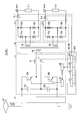
- FIG. 1A is a diagram showing an entire configuration of a power supply device for an electric vehicle according to a first embodiment.
- the electric vehicle power supply device 1 includes a current collector CC to which electric power is supplied from an overhead wire F (not shown) and a wheel W (not shown) grounded via a line R (not shown). Connected in series in the current path between In FIG. 1A, a pole which becomes substantially the same potential as the line R and the wheel W side is indicated by a symbol of a ground pole.
- the power supply device 1 for an electric vehicle includes, for example, a power conversion circuit 2, a resonant inverter 3, a transformer 4, a rectifier 5 (rectifier circuit), a control unit 6, and a current detector 7 (first current detector) And.
- the symbol Z indicates a load.
- the power conversion circuit 2 is connected to a subsequent stage of the current collector CC, and converts the power received by the current collector CC into DC power of a predetermined voltage.
- a resonant inverter 3 which receives a direct current is connected.
- the power conversion circuit 2 may convert AC power received by the current collector CC as an AC DC power converter into DC power, or the first DC received by the current collector CC as a DC voltage converter The power may be converted to the second DC power.
- the case where the current collector CC receives the first DC power will be described as an example.
- the resonant inverter 3 converts the second DC power, which is the output of the power conversion circuit 2, into first AC power and outputs it.
- the frequency of the first AC power matches the switching frequency of the switching element 32a and the switching element 32b described later.
- the primary side terminal forming the set of transformers 4 is connected to the output terminal forming the set of resonant inverters 3.
- the transformer 4 includes at least a primary winding 41 (first winding) and a secondary winding 42 (second winding) electrically isolated from each other and magnetically coupled.
- the transformer 4 is included in the resonant circuit, and the first AC power generated by the resonant inverter 3 is supplied to the primary side terminal connected to the primary winding 41.
- Transformer 4 converts the first AC voltage output from resonant inverter 3 with the turns ratio of primary winding 41 and secondary winding 42, and converts the converted second AC power into a secondary winding. It supplies from the secondary side terminal connected to the wire 42.
- a rectifier 5 is connected to a secondary side terminal forming a set of transformers 4.
- the rectifier 5 full-wave rectifies the second AC power output from the transformer 4.
- the rectifier 5 includes diodes 51a and 52a constituting an upper arm and diodes 51b and 52b constituting a lower arm, the diode 51a and the diode 51b are connected in series, and the diode 52a and the diode 52b are respectively in series It is connected to the.
- the load Z is connected to the subsequent stage of the rectifier 5, and the power after the rectifier 5 rectifies is supplied to the load Z.
- a filter (not shown) may be connected that removes high frequency components (noise) from the output of the rectifier 5 and outputs the result to the load Z.
- a power conversion circuit (not shown) may be connected between the output of the rectifier 5 and the input of the load.
- the control unit 6 includes, for example, a storage unit 61, a CPU (central processing unit) 62, a drive unit 63, and a current value acquisition unit 64.
- the storage unit 61, the CPU 62, the drive unit 63, and the current value acquisition unit 64 are connected via a BUS.
- the storage unit 61 includes a semiconductor memory.
- the CPU 62 includes a processor that executes a desired process in accordance with a software program.
- the drive unit 63 generates a control signal of the resonant inverter 3 in accordance with the control of the CPU 62.
- the current value acquisition unit 64 acquires the detection result of the current detector 7.
- the CPU 62 of the control unit 6 controls the resonant inverter 3 by the drive unit 63 based on the detection result of the current detector 7 acquired by the current value acquisition unit 64.
- the processing performed by the CPU 62, the drive unit 63, and the current value acquisition unit 64 may be collectively described simply as the processing of the control unit 6.
- the control unit 6 is described as controlling the resonant inverter 3 based on the detection result of the current detector 7.
- the control unit 6 controls the entire power supply device 1 for an electric vehicle.
- the resonant inverter 3 includes, for example, capacitors 31a and 31b, switching elements 32a and 32b, a resonant reactor 33, a control frequency adjustment unit 35, and a drive circuit 36.
- the capacitors 31a, 31b are connected in series with one another to form a filter capacitor.
- the first end of the series of capacitors 31a and 31b is connected to the first pole of the output terminal of the power conversion circuit 2, and the second end is connected to the second pole of the output terminal of the power conversion circuit 2. Be done.
- the capacitors 31a and 31b may have the same capacitance and uniform characteristics.
- the switching element 32a and the switching element 32b are connected in series with each other.
- the switching element 32 a is connected to the first pole of the output terminal of the power conversion circuit 2 to form a so-called upper arm.
- the switching element 32 b is connected to the second pole of the output terminal of the power conversion circuit 2 to form a so-called lower arm.
- the switching element 32a and the switching element 32b may be IGBTs (Insulated Gate Bipolar Transistors), IEGTs (Injection Enhanced Gate Transistors), MOSFETs (Metal-Oxide-Semiconductor Field-Effect Transistors), etc. It is.
- the switching element 32 a and the switching element 32 b are switched between the conduction state and the interruption state at the timing generated by the control frequency adjustment unit 35.
- the control frequency adjustment unit 35 receives a control signal from the drive unit 63 of the control unit 6, adjusts the frequency of the control pulse supplied to the drive circuit 36, and supplies the control circuit whose frequency is adjusted to the drive circuit 36.
- the control frequency adjustment unit 35 includes a transmitter (not shown) and a divider capable of changing the division ratio.
- the control frequency adjustment unit 35 adjusts the division ratio under the control of the control unit 6 to generate a control pulse of a predetermined frequency.
- the frequency is a frequency selected from among a plurality of predetermined frequency candidates.
- the control frequency adjustment unit 35 sets the above frequency as a switching frequency for controlling the switching element 32 a and the switching element 32 b.
- the drive circuit 36 supplies a gate signal corresponding to the control pulse supplied from the control frequency adjustment unit 35 to the switching element 32 a and the switching element 32 b.
- the switching element 32 a and the switching element 32 b switch between the on state and the off state based on the gate signal supplied from the drive circuit 36.
- control frequency adjustment unit 35 can adjust the difference between the resonant frequency of the resonant circuit and the switching frequency of the switching element 32 a and the switching element 32 b by switching the switching frequency.
- control frequency adjustment unit 35 can select the frequency f L having a relatively low frequency and the frequency f H higher than the frequency f L as the switching frequency.
- the control frequency adjustment unit 35 is an example of the influence suppression unit.
- the resonance reactor 33 is connected between a connection point of the switching element 32 a and the switching element 32 b and the first end of the primary side terminal of the transformer 4.
- the second end of the primary side terminal of the transformer 4 is connected to the connection point (middle point) of the capacitors 31a and 31b.
- resonance reactor 33 may be omitted.
- the control unit 6 detects the current flowing through the transformer 4 by the current detector 7.
- the current detector 7 shown in FIG. 1A detects the current flowing in the primary winding of the transformer 4. For example, when the power supply (output) from the transformer 4 is stopped, the influence of the power supply stop may affect the primary side of the transformer 4.
- the control unit 6 suppresses the influence by controlling the gate voltage of the switching elements 32 a and 32 b according to the detected current value of the current flowing through the primary winding of the transformer 4.
- control unit 6 adjusts the switching frequency of the resonant inverter 3 based on the detected current value of the current flowing through the primary winding of the transformer 4. The details will be described later.
- the resonant inverter 3 shown in FIG. 1A is an example of a half bridge type voltage inverter.
- the resonant inverter 3 is not limited to that shown in FIG. 1A, and may be, for example, a full-bridge voltage-type inverter or a current-type inverter.
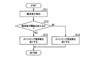
- FIG. 1B is a flowchart showing the process of adjusting the switching frequency according to the embodiment.
- the current detector 7 detects the current of the primary winding of the transformer 4.
- the CPU 62 of the control unit 6 acquires the current value detected by the current detector 7 by the current value acquisition unit 64 and records it as time series data in the storage unit 61 (step S11).
- the CPU 62 of the control unit 6 determines whether the acquired current value exceeds the threshold I TH (step S12).
- the threshold I TH is determined based on the rated current value of the resonant inverter 3 or the like.
- the threshold value I TH is equal to or less than the rated current of the resonant inverter 3 and exceeds the fluctuation range of the load current in the normal state.
- the control unit 6 adjusts the value of the switching frequency to be lower than the value before adjustment (step S13). For example, the control unit 6 sends a control signal specifying the frequency f L as the switching frequency to the control frequency adjustment unit 35, and adjusts the switching frequency generated by the control frequency adjustment unit 35.
- the value of the switching frequency in this case may be a predetermined value.
- the lower limit value of the switching frequency may be set, and the value of the switching frequency may be gradually adjusted in a predetermined step until reaching the lower limit value. This completes the series of processes shown in the figure.
- the control unit 6 adjusts the value of the switching frequency to be higher than the value before adjustment (step S14). For example, the control unit 6 sends a control signal specifying the frequency f H as the switching frequency to the control frequency adjustment unit 35, and adjusts the switching frequency generated by the control frequency adjustment unit 35.
- the value of the switching frequency in this case may be a predetermined value in a frequency range in which the switching of the switching elements 32a and 32b is soft switching.
- the upper limit value of the switching frequency at which the switching of the switching elements 32a and 32b becomes soft switching is set, and the control unit 6 adjusts the switching frequency value in the range up to the above upper limit value. Good.
- the control unit 6 may adjust the value of the switching frequency gradually in a predetermined step so that the value of the switching frequency approaches the above upper limit value. The series of processing shown in the figure is completed.
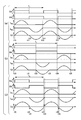
- FIG. 1C is a diagram for explaining the adjustment process of the switching frequency according to the embodiment.
- I TH is a threshold used to determine the current value.
- the control unit 6 can select one of the frequency f H and the frequency f L as the switching frequency (fs).
- the control unit 6 selects the frequency f H as the switching frequency.
- the control unit 6 identifies the state of the resonant inverter 3 at a predetermined cycle.
- Time t1 and time t2 shown in the figure are timings defined by the above-mentioned predetermined cycle. The time from the time t1 to the time t2 (predetermined period) is sufficiently longer than the switching period of the switching elements 32a and 32b (period defined based on the frequency f H and the frequency f L ).
- the control unit 6 identifies that the current value detected by the current detector 7 is larger than the threshold I TH and selects the frequency f L as the switching frequency. For example, the control unit 6 determines that the switching of the switching elements 32a and 32b is hard switching based on the result of identifying that the current value at the time of switching of the resonant inverter 3 exceeds the threshold I TH. The value of the switching frequency of the resonant inverter 3 is set to the frequency f L. Thereby, the switching of the switching elements 32a and 32b shifts from hard switching to soft switching. The control unit 6 maintains the value of the switching frequency and continues the frequency f L until time t2, which is the next detection time.
- the control unit 6 identifies that the current value detected by the current detector 7 is smaller than the threshold value I TH , and selects the frequency f H as the switching frequency.
- the controller 6 maintains the value of the switching frequency and continues the frequency f H until the next detection timing is reached.
- the frequency selected by the control unit 6 when decreasing the value of the switching frequency may be a predetermined value as described above, or the frequency may be reduced by a predetermined amount from the current frequency.
- the difference value may be predetermined, and may be a value calculated based on the current frequency and the above difference value.
- FIG. 1D is a diagram for explaining the adjustment processing of the switching frequency according to the embodiment.
- FIG. 1D three timing charts under different conditions are drawn.
- the timing chart of (a) in FIG. 1D an example of a state where soft switching is established in switching of the switching elements 32a and 32b in a state where the control unit 6 selects the frequency f H as the switching frequency. Is drawn.
- the control cycle in this case is T1.
- Gate signals (32a, 32b) of the switching elements 32a, 32b are respectively drawn on the top and the second stage of the timing chart of (a) in FIG. 1D.
- the description of the guard time between gate signals in this figure is abbreviate
- the switching elements 32a and 32b are in the conductive state when the signal level of the gate signal is at the H level, and are in the blocking state when the signal is at the L level.
- the waveform (I 33 ) of the current flowing through the resonance reactor 33 is equivalent to the current (I 33 ) flowing through the primary winding of the transformer 4.
- the waveform (I 33 ) of the current flowing through the resonance reactor 33 is an example of the waveform of the load current.
- the control unit 6 controls the switching element 32a to be in the conductive state and the switching element 32b to be in the cut off state. During this period, current I 32a flows during a period up to half of the resonance period of the resonant circuit after switching element 32a becomes conductive, but after that period, switching element 32a is reverse biased and current flow Stops (time t11). A period from time t11 to time t12 is a period in which no current flows. From time t10 to time t12, the order switching device 32b is in the blocking state, the waveform of the current I 33 shown in the fifth row, the same shape as the waveform of the current I 32a.
- the control unit 6 controls the switching element 32b to be in the conductive state and the switching element 32a to be in the cut off state.
- the waveform of each signal from time t12 to time t14 is different in polarity as compared with the current waveform from time t10 to time t12, but is generated similarly to the waveform of each signal from time t10 to time t12 described above.
- the current I 32 b is detected by the current detector 7 as a signal having a negative polarity.
- the current I 32a and the current I 32b are substantially zero at time t11 when the switching element 32a is cut off and at time t13 when the switching element 32b is cut off.
- switching element 32a controlled to be in a conducting state causes current I 32a to flow.
- the same process is repeated after time t16.
- the waveform depicted in (a) in FIG. 1D is a case where soft switching is established in switching of the switching elements 32a and 32b.
- the length of the period in which the current flows is the same as that in the case of (a) in FIG.
- the length of the non-period is longer than in the case of (a) in FIG. 1D.
- the resonance condition of the resonant circuit is different from the case of (a) in FIG.
- An example of a situation that is longer than the case is drawn.
- a state where the control unit 6 selects the frequency f H as the switching frequency is illustrated.
- the illustrated waveform depicts an example of a state in which the switching of the switching elements 32a and 32b does not hold soft switching.
- Times t30, t32, t34, and t36 indicate times in the order described, and correspond to the aforementioned times t10, t12, t14, and t16, respectively.
- Times t31, t33 and t35 indicate times after times t32, t34 and t36.
- the control cycle in the case shown in (c) in FIG. 1D is T3 equal to T1.
- the control unit 6 controls each of the switching element 32a in the conductive state and the switching element 32b in the cut-off state from time t30 to time t32. It is.
- the waveform of the current I 32 a of (c) in FIG. 1D focuses on the time of time t32.
- the resonant reactance 33 causes current in the same direction as the current I 32a by the action of the resonant circuit from time t32 to time t31.
- the electromotive force increases the potential on the switching elements 32 a and 32 b of the resonant reactance 33.
- the switching element 32b is in a conducting state from time t32 to time t34, an excessive current may flow in the switching element 32b due to the above-mentioned electromotive force.
- the current from time t32 to time t31 may be larger than the current value of the waveform that the resonance circuit originally produces in the state where there is no electromotive force. Since the same phenomenon occurs thereafter, the current I 33 has an instantaneous value (absolute value), an effective value, and an average value larger than those in the case where the soft switching is established. Depending on the conditions, the peak value may also be larger than when the soft switching is established.
- the desired action to suppress the influence of the fluctuation of the load current is not taken. It includes a predetermined range that leads to an increase in power conversion loss.
- the value of the actual resonance frequency deviates from the design value, and conversion in the resonance type inverter 3 Losses may increase.
- the control unit 6 of the power supply device 1 for an electric vehicle controls the resonance circuit so that the current flowing through the switching elements 32a and 32b becomes equal to or less than a predetermined value when the switching elements 32a and 32b of the resonant inverter 3 are switched.
- the switching elements 32a and 32b of the resonant inverter 3 are soft-switched by putting the difference between the resonant frequency and the switching frequency in a predetermined range.
- the switching frequency so as to switch the switching elements 32a and 32b, the state of soft switching of the switching of the switching elements 32a and 32b is maintained.
- the resonant inverter 3 can reduce the switching loss of the switching elements 32a and 32b.
- the control unit 6 can simplify the cooling system of the resonant inverter 3 by optimizing the value of the switching frequency, and can realize the miniaturization and the weight reduction.
- the control frequency adjustment unit 35 may perform the above-described optimization process of the switching frequency of the control unit 6.
- the threshold value for determining the value of the current flowing through the transformer 4 may be determined in advance within the range of the current value at which hard switching does not occur in the switching elements 32a and 32b.
- the load Z of the embodiment may include a power storage unit electrically connected in parallel to the load Z.
- the supply of power from the rectifier 5 to the load Z is stopped.
- the load Z in addition to the case where the load Z is disconnected by a mechanical switch or the like, the supply of power from the rectifier 5 to the load Z may be stopped. According to the present embodiment, even when the load Z as described above includes the power storage unit, the influence of the stop of the supply of power can be suppressed.
- the resonant inverter 3 of the first embodiment adjusts the switching frequency of the resonant inverter in a fixed or semi-fixed manner at a predetermined switching frequency.
- a predetermined switching frequency instead of this, in the first modification, an example in which the switching frequency of the resonant inverter is adjusted to be optimized will be described.
- the efficiency can be further improved by making the current waveform a waveform closer to a sine wave. Therefore, the control unit 6 searches for the upper limit value of the resonance frequency at which the switching of the switching elements 32a and 32b becomes soft switching, and the waveform of the current flowing on the primary side of the transformer 4 becomes a waveform closer to a sine wave Do.
- the electric vehicle power supply device 1 includes a current detector 7 that detects the current flowing through the primary winding 41 of the transformer 4.
- the control unit 6 is configured such that switching of the resonant inverter 3 is soft within the range of the switching frequency that is permitted for control to periodically switch the switching elements 32a and 32b based on the current value detected by the current detector 7. Search for the switching frequency to be switched. Furthermore, the control unit 6 selects a higher switching frequency.
- the control unit controls the switching frequency higher than the frequency at which the switching of the switching elements 32a and 32b of the resonant inverter is soft switching. 6 makes it possible to optimize the switching frequency so that the output voltage waveform approaches a sine wave. For example, when the period obtained by adding the dead timing for preventing hard switching to the half cycle corresponding to the resonance frequency of the resonant circuit coincides with the half cycle of the switching frequency, the highest switching frequency can be achieved.
- the resonant inverter 3 of the embodiment is an example of a half bridge type voltage inverter.
- the resonant inverter 3 is not limited to the one described in FIG. 1A, and may be, for example, a full-bridge voltage-type inverter or a current-type inverter.
- the control unit 6 can measure the voltage instead of measuring the current as described above, and can control in the same manner based on the voltage.
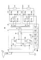
- FIG. 2 is a diagram showing an entire configuration of a power supply device for an electric vehicle according to a second embodiment.
- the present embodiment differs from the above-described first embodiment shown in FIG. 1A in that there are a plurality of output systems of the transformer 4. In the following, this point will be described in detail.
- the power supply device 1A for an electric vehicle includes the power conversion circuit 2, the resonant inverter 3, the transformer 4A, the rectifier 5-1 (rectifier circuit), the rectifier 5-2 (rectifier circuit), and the control unit 6A. , A current detector 7, a current detector 8-1 (second current detector), and a current detector 8-2 (third current detector).
- Transformer 4A includes at least a primary winding 41, a secondary winding 42 (second winding) and a tertiary winding 43 (third winding) electrically isolated from each other and magnetically coupled.
- Transformer 4A converts the AC voltage output from resonant inverter 3 by the turns ratio of primary winding 41 and secondary winding 42, and converts the converted second AC power into secondary winding 42. It supplies from the secondary side terminal connected to.
- a rectifier 5-1 is connected to the secondary side terminal of the transformer 4A.
- Transformer 4A converts the AC voltage output from resonant inverter 3 by the turns ratio of primary winding 41 and tertiary winding 43, and converts the converted third AC power into tertiary winding 43. It supplies from the tertiary side terminal connected to.
- a rectifier 5-2 is connected to the tertiary terminal of the transformer 4A.
- the rectifier 5-1 and the rectifier 5-2 perform full-wave rectification of the AC power output from the transformer 4A, as with the rectifier 5 described above.
- a current detector 8-1 and a load Z-1 are provided downstream of the rectifier 5-1 shown in FIG.
- the second AC power (output 1) is supplied to the load Z-1.
- the current detector 8-1 detects a load current (second load current) flowing from the rectifier 5-1 to the load Z-1.
- a current detector 8-2 and a load Z-2 are provided downstream of the rectifier 5-2.
- the third AC power (output 2) is supplied to the load Z-2.
- the current detector 8-2 detects a load current (third load current) flowing from the rectifier 5-2 to the load Z-2.
- a filter (not shown) that removes high frequency components (noises) from the output of the rectifier 5-1 and outputs the result to the load Z-1 may be connected to the rear stage of the rectifier 5-1.
- a filter (not shown) that removes high frequency components (noise) from the output of the rectifier 5-2 and outputs the result to the load Z-2 may be connected to the rear stage of the rectifier 5-2.
- the control unit 6A corresponds to the control unit 6 described above.
- the control unit 6A includes a current value acquisition unit 64A in place of the current value acquisition unit 64 of the control unit 6 described above.
- the current value acquisition unit 64A corresponds to the above-described current value acquisition unit 64.
- the current value acquisition unit 64A acquires the detection results of the current detector 7, the current detector 8-1, and the current detector 8-2.
- the CPU 62 of the control unit 6 controls the resonant inverter 3 by the drive unit 63 based on the detection results of the current detector 7, the current detector 8-1, and the current detector 8-2 acquired by the current value acquisition unit 64.
- Control For example, the control unit 6A calculates the load current based on the detection results of the current detector 7, the current detector 8-1, and the current detector 8-2.
- the control unit 6A relatively lowers the switching frequency when at least the load current exceeds a predetermined value.
- three current detectors 7, 8-1 and 8-2 are provided.
- the current detectors 7, 8-1, 8-2 detect the current flowing in the winding of the transformer 4A at each position.
- the control unit 6A acquires the current values detected by the above-described three current detectors, and records the current values in the storage unit 61 as time-series data (step S11).
- the control unit 6A determines, for example, whether any of the acquired current values exceeds a threshold (step S12).
- control unit 6A adjusts the switching frequency to be relatively low (step S13), and completes the series of processes shown in the figure.
- control unit 6A adjusts the switching frequency to be relatively high (step S14), and completes the series of processes shown in the figure.
- control unit 6A can apply the method of the embodiment even when the transformer 4A has a plurality of secondary side systems.
- the present invention is applicable not only to the case of the secondary winding and the tertiary winding shown in FIG. 2 but also to the case of providing more windings such as a quaternary winding. Note that the method of the first embodiment may be applied to the adjustment of the current value.
- the power consumption of the loads Z-1 and Z-2 in any system Fluctuation may cause the power supply to stop.
- the inductance of the winding of the system is apparently invalidated.
- the combined inductance based on the primary side conversion of the transformer 4A becomes larger than when the output of the system is valid.
- the resonant frequency of the resonant circuit is lowered, there is a possibility that the resonant inverter 3 shifts from soft switching to hard switching.
- control unit 6A determines that the current of any system falls below a predetermined value by using the current detectors 8-1 and 8-2 provided in the respective systems by the above-described processing, and the resonant inverter Hard switching can be prevented by changing the switching frequency of.
- any one of the load currents detected by the respective current detectors is switched in the control unit 6A of the power supply device 1A for an electric vehicle If the difference between the resonant frequency of the resonant circuit and the switching frequency falls within a predetermined range, at least one of the resonant frequency and the switching frequency of the resonant circuit is adjusted. As a result, even if the output of any system is stopped and the matching between the resonant frequency and the switching frequency of the resonant inverter can not be achieved and the hard switching is performed as in the first embodiment, the power supply device 1A for an electric vehicle By adjusting the switching frequency, soft switching can be maintained and an increase in switching loss can be prevented.
- the controller 6A adjusts the values of the second load current and the third load current flowing by switching of the switching elements 32a and 32b by adjusting at least one of the value of the resonant frequency of the resonant circuit and the value of the switching frequency. By setting the value to a predetermined value or less, soft switching of the switching elements 32a and 32b can be maintained.
- FIG. 3A is a diagram showing an entire configuration of a power supply device for an electric vehicle according to a third embodiment.
- the present embodiment is different from the second embodiment shown in FIG. 2 described above in the configuration of the capacitor. In the following, this point will be described in detail.
- the electric vehicle power supply device 1B includes, for example, a power conversion circuit 2, a resonant inverter 3B, a transformer 4A, a rectifier 5-1, a rectifier 5-2, a control unit 6B, and a current detector 7.
- a current detector 8-1 and a current detector 8-2 are provided.
- the resonant inverter 3B includes, for example, capacitors 31a, 31b, 31c, 31d, switching elements 32a, 32b, a resonant reactor 33, and contactors 34a, 34b (first contactors).
- the capacitors 31a and 31b (first resonant capacitors) are connected in series with each other.
- the first end of the series of capacitors 31a and 31b is connected to the first pole of the output terminal of the power conversion circuit 2, and the second end is connected to the second pole of the output terminal of the power conversion circuit 2. Be done.
- the capacitors 31c, 31d (second resonant capacitors) are connected in series with each other.
- the first end of the pair of capacitors 31 c and 31 b connected in series is connected to the first pole of the output terminal of the power conversion circuit 2, and the second end is connected to the second pole of the output terminal of the power conversion circuit 2 Be done.
- the connection point (middle point) of the capacitors 31c and 31d is connected to the connection point (middle point) of the capacitors 31a and 31b and the second end of the primary side terminal of the transformer 4A.
- the set of capacitors 31c, 31d is combined with the set of capacitors 31a, 31b to form a filter capacitor.
- the capacitors 31a, 31b, 31c, and 31d may be collectively referred to as a capacitor 31.
- a contactor 34a associated with the capacitor 31c and a contactor 34b associated with the capacitor 31d are provided.
- the contactor 34 a is connected in series to the capacitor 31 c and is disposed between the first pole of the output terminal of the power conversion circuit 2 and the midpoint.
- the contactor 34 b is connected in series to the capacitor 31 d and is disposed between the second pole of the output terminal of the power conversion circuit 2 and the midpoint.
- the contactors 34a and 34b may be those which can open and close the circuit, such as semiconductor switching elements.
- the capacitors 31c and 31d are electrically connected in parallel to the capacitors 31a and 31b, and the capacity of the capacitor 31 is increased as compared with the case of only the combination of the capacitors 31a and 31b.
- the capacitor 31c in parallel to the capacitor 31a and the capacitor 31d to the capacitor 31b, the value of the resonance frequency can be lowered by the increase in the capacity of the capacitor 31.
- the capacitors 31c and 31d can be used for fine adjustment of the resonance frequency.
- the capacitances of the respective capacitors 31 may be the same.
- the control unit 6B corresponds to the control units 6 and 6A described above.
- the control unit 6B includes, for example, a storage unit 61, a CPU 62, a drive unit 63, a current value acquisition unit 64A, and a switch drive unit 65.
- the storage unit 61, the CPU 62, the drive unit 63, the current value acquisition unit 64A, and the switch drive unit 65 are connected via a BUS.
- the switch driver 65 sends a control signal to the contactors 34a and 34b to switch between the open state and the closed state of the contacts of the contactors 34a and 34b.
- the processing performed by the CPU 62, the drive unit 63, the current value acquisition unit 64, and the switch drive unit 65 may be collectively described simply as processing of the control unit 6B.
- the control unit 6B opens the contactors 34a and 34b to release the parallel connection of the capacitors 31c and 31d.
- FIG. 3B is a flowchart showing the adjustment processing of the switching frequency according to the embodiment.
- the control unit 6B acquires the current value detected by the current detector 7 and records the value as time series data in the storage unit 61 (step S31). The controller 6B determines whether the acquired current value exceeds a threshold (step S32).
- the controller 6B opens the contactors 34a and 34b (switches) (step S33), and completes the series of processes shown in the figure.
- the controller 6B closes the contactors 34a and 34b (switches) (step S34), and completes the series of processes shown in the figure.
- control unit 6B can prevent hard switching by changing the resonant frequency of the resonant inverter.
- control unit 6B determines that it is hard switching and automatically lowers the switching frequency of the resonant inverter. This shifts from hard switching to soft switching.
- FIG. 3C is a diagram for explaining the adjustment process of the switching frequency according to the embodiment.
- the timing chart shown in FIG. 3C depicts an example of changes in the current value detected by the current detector 7, the state of the circuit breaker, and the resonant frequency of the resonant circuit.
- the control unit 6B is selecting the frequency f 1 as the resonant frequency.
- the control unit 6 identifies the state of the resonant inverter 3 at a predetermined cycle.
- Time t1 and time t2 shown in the figure are timings defined by the above-mentioned predetermined cycle. Time from time t1 to time t2 (the predetermined period) is sufficiently longer than the switching elements 32a, 32b switching period of (period defined on the basis of the resonance frequency f 1 and the resonance frequency f 2).
- the resonance frequency f 1 as compared with the resonance frequency f 2, it is assumed the frequency is low. It is assumed that the current value detected by the current detector 7 has transitioned to a state higher than the threshold I TH by time t1. At time t1, the control unit 6 identifies that the current value detected by the current detector 7 has transitioned to a state higher than the threshold I TH . Control unit 6 selects the resonant frequency f 2 as the switching frequency. For example, the control unit 6B uses the current detectors 7, 8-1 and 8-2 provided in each system to identify that the current value of any system has exceeded the threshold value I TH .
- control unit 6B determines that the switching of the switching elements 32a and 32b is hard switching, and the contactor is determined based on the result of the determination. Control 34a and 34b in the open state.
- the control unit 6B can automatically increase the resonance frequency of the resonant circuit of the resonant inverter by setting the value of the switching frequency of the resonant inverter 3 to the frequency f 1 and prevent the hard switching state from continuing. (Time t2).
- the processing after time t2 refers to the above description.
- control part 6B controls contactors 34a and 34b, when load current exceeds a predetermined value.
- the power supply of any system of the secondary side of the transformer 4A is stopped, and the matching between the resonant frequency and the switching frequency of the resonant inverter 3B Even under the condition that the hard switching occurs due to the collapse of the capacitor 31, the resonant frequency of the resonant circuit can be adjusted by changing the capacitance of the capacitor 31. This can maintain soft switching and prevent an increase in switching loss.
- the arrangement of the contactors 34a and 34b is not limited to the above example.
- one or both of the capacitors 31a and 31b and the capacitors 31c and 31d of the resonant inverter 3 may be provided with contactors 34a and 34b that release the parallel connection.
- the control unit 6B controls so that at least one of the pair of capacitors 31a and 31b and the pair of capacitors 31c and 31d is connected to the primary side of the transformer 4A.
- the number of switching stages of the resonance frequency can be at least three by setting the capacitances of the pair of capacitors 31a and 31b and the capacitance of the pair of capacitors 31c and 31d to different values.
- FIG. 4A is a diagram showing an entire configuration of a power supply device for an electric vehicle according to a fourth embodiment.
- the present embodiment differs from the second embodiment shown in FIG. 2 in that a capacitor is provided on the output side of the transformer 4A.
- this point will be described in detail.
- the electric vehicle power supply device 1C includes, for example, a power conversion circuit 2, a resonant inverter 3, a transformer 4A, a rectifier 5-1, a rectifier 5-2, a control unit 6C, and a current detector 7.
- a capacitor 9-1 (parallel capacitor) and a capacitor 9-2 (parallel capacitor) are provided.
- the capacitor 9-1 is connected in parallel to the secondary winding 42 of the transformer 4A.
- the capacitor 9-1 is a parallel circuit of the secondary winding 42 of the transformer 4.
- the capacitor 9-2 is connected in parallel to the tertiary winding 43 of the transformer 4A.
- the capacitor 9-2 is a parallel circuit of the tertiary winding 42 of the transformer 4.
- capacitors 9-1 and 9-2 are added to the output side of the transformer 4A in the second embodiment.
- the capacitors 9-1 and 9-2 are an example of the influence suppression unit.
- the control unit 6C corresponds to the control unit 6 described above.
- the control unit 6C includes, for example, a storage unit 61, a CPU 62, a drive unit 63, a current value acquisition unit 64, and a switch drive unit 66.
- the storage unit 61, the CPU 62, the drive unit 63, the current value acquisition unit 64, and the switch drive unit 66 are connected via a BUS.
- the processing performed by the CPU 62, the drive unit 63, the current value acquisition unit 64, and the switch drive unit 66 may be collectively described simply as processing of the control unit 6B.
- the switch drive unit 66 will be described later. It is not essential that the control unit 6C of the embodiment has a function for adjusting the switching frequency of the resonant inverter 3.
- the capacitors 9-1 and 9-2 on the output side of the transformer 4A as described above, when power supply to any one of the plurality of secondary side systems of the transformer 4A stops, Since the inductance of the winding of the transformer 4A is validated by the flow of alternating current through the capacitors 9-1 and 9-2 provided in the system, the resonant frequency of the resonant inverter 3 does not change.
- the load Z-1 is connected to the secondary winding 42 of the transformer 4A through the rectifier 5-1, and the load Z-1 is connected to the tertiary winding 43 through the rectifier 5-2. -2 is connected.
- Power supply device 1C for electric vehicles further includes a capacitor 9-1, which is a parallel circuit connected in parallel to secondary winding 42 of transformer 4A, and a capacitor, which is a parallel circuit connected in parallel to tertiary winding 43. And 9-2.
- capacitors 9-1 and 9-2 are provided only in the system where the supply of power is stopped.
- the capacitors 9-1 and 9-2 of the embodiment are fixedly connected to the secondary side of the transformer 4A.
- capacitors 9-1 and 9-2 of the modification are appropriately connected to the secondary side of transformer 4A.
- FIG. 4B is a block diagram of a capacitor according to a modification of the fourth embodiment.
- the capacitor 9-1 shown in FIG. 4B includes, for example, a capacitor body 9a and a contactor 9b connected in series to the capacitor body 9a.
- the contactor 9b may be, for example, a semiconductor switching element or the like as long as it can open and close the circuit.
- the switch driving unit 66 of the control unit 6C in the modification sends a control signal to the contactors 9b provided in the capacitors 9-1 and 9-2, respectively, to switch between the open state and the closed state of the contacts of the contactor 9b.
- the control unit 6C opens the contactor 9b when the current value detected by the current detector 7 exceeds a predetermined value (threshold value I TH ) as in FIG. 3B described above.
- the controller 6C closes the contactor 9b when the current value detected by the current detector 7 is equal to or less than a predetermined value (threshold I TH ).
- control unit 6C determines that hard switching is occurring when the current value exceeds the threshold, and performs control to lower the resonance frequency. Do.
- the control unit 6C can perform hard switching. Connect when it is detected that it has occurred. Since the capacitors 9-1 and so forth become loads of the transformer 4A, losses due to the capacitors 9-1 and the like occur at the time of connection. In the modification, it is not necessary to always connect the capacitor 9-1 and the like to the transformer 4A, and the conversion loss can be reduced as compared with the case where it is always connected.
- the switch drive unit 66 and the capacitors 9-1 and 9-2 of the control unit 6C are an example of the influence suppression unit.
- FIG. 5A is a diagram showing an entire configuration of a power supply device for an electric vehicle according to a fifth embodiment.
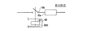
- the present embodiment is different from the fourth embodiment in that a resistor 10-1 and the like are provided instead of the capacitor 9-1 and the like of the fourth embodiment.
- a resistor 10-1 and the like are provided instead of the capacitor 9-1 and the like of the fourth embodiment.
- the electric vehicle power supply device 1D includes, for example, a power conversion circuit 2, a resonant inverter 3, a transformer 4A, a rectifier 5-1, a rectifier 5-2, a control unit 6D, and a current detector 7.
- a resistor 10-1 (parallel resistor) and a resistor 10-2 (parallel resistor) are provided.
- the resistors 10-1 and 10-2 are electric resistors.
- the capacitors 9-1 and 9-2 are provided on the secondary side of the transformer 4A.
- the power supply device 1D for an electric vehicle according to the present embodiment In place of this, resistors 10-1 and 10-2 are provided. The other points are the same as in the fourth embodiment.
- the resistors 10-1 and 10-2 are added to the output side of the transformer 4A.
- the resistors 10-1 and 10-2 are an example of the influence suppression unit.
- the control unit 6D corresponds to the control unit 6C described above.
- the control unit 6D includes a switch drive unit 67 instead of the switch drive unit 66 of the control unit 6C described above.
- the switch drive unit 67 corresponds to the switch drive unit 66 described above.
- the switch drive unit 67 will be described later. It is not essential that the control unit 6D of the embodiment has a function for adjusting the switching frequency of the resonant inverter 3.
- the resistors 10-1 and 10-2 on the output side of the transformer 4A as described above, the power supply of any of the plurality of secondary side systems of the transformer 4A may be stopped. Even if it occurs, the alternating current flows through the resistors 10-1 and 10-2 provided in the system, so that the inductance of the winding of the transformer 4A is validated, so that the resonant frequency of the resonant inverter 3 Does not change.
- the load is connected to the secondary winding 42 of the transformer 4A through the rectifier 5-1 and the rectifier 5-1, and the rectifier 5-2 and the rectifier are connected to the tertiary winding 43.
- the load is connected through 5-2.
- the electric vehicle power supply device 1D is a parallel circuit further connected in parallel to the resistor 10-1, which is a parallel circuit connected in parallel to the secondary winding 42 of the transformer 4A, and a tertiary winding 43. And a resistor 10-2.
- resistors 10-1 and 10-2 be provided only in the system where the supply of power is stopped.
- the resistors 10-1 and 10-2 of the embodiment are fixedly connected to the secondary side of the transformer 4A.
- the resistors 10-1 and 10-2 of the modification are appropriately connected to the secondary side of the transformer 4A.
- FIG. 5B is a block diagram of a resistor according to a modification of the fourth embodiment.
- the resistor 10-1 shown in FIG. 5B includes a resistor body 10a and a contactor 10b connected in series to the resistor body 10a.
- the contactor 10b may be, for example, a semiconductor switching element or the like as long as it can open and close the circuit.
- the switch drive unit 67 of the control unit 6D in the modification sends a control signal to the contactor 10b provided in each of the resistors 10-1 and 10-2, and the open state and the closed state of the contact of the contactor 10b are detected.
- Switch For example, the control unit 6D in the modification opens the contactor 10b when the current value detected by the current detector 7 exceeds a predetermined value (threshold). The control unit 6D closes the contactor 10b when the current value detected by the current detector 7 is equal to or less than a predetermined value (threshold value).
- control unit 6D determines that hard switching is occurring when the current value exceeds the threshold, and performs control to lower the resonance frequency. Do.
- the control unit 6D performs hard switching. Connect if it is detected that Since the resistor 10-1 and the like become loads of the transformer 4A, a loss due to the resistor 10-1 and the like occurs at the time of connection. In the modification, it is not necessary to always connect the resistor 10-1 and the like to the transformer 4A, and the conversion loss can be reduced as compared to the case where it is always connected.
- the switch drive unit 67 and the resistors 10-1 and 10-2 of the control unit 6C are an example of the influence suppression unit.
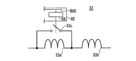
- FIG. 6A is a view showing a reactor of the sixth embodiment.
- the present embodiment is different from the second embodiment shown in FIG. 2 described above in the configuration of the reactor. In the following, this point will be described in detail.
- the power supply device 1E for an electric vehicle includes, for example, the power conversion circuit 2, the resonant inverter 3, the transformer 4A, the rectifier 5-1, the rectifier 5-2, the control unit 6E, and a current detector. , A current detector 8-1, and a current detector 8-2.
- the resonant inverter 3 includes, for example, capacitors 31 a and 31 b, switching elements 32 a and 32 b, and a resonant reactor 33.
- the resonance reactor 33 of the embodiment includes, for example, a reactor 33a, a reactor 33b, and a contactor 33c (second contactor).
- the reactor 33-1 and the reactor 33-2 are electrically connected in series, and combine to function as a resonance reactor 33.
- the contactor 33c is provided to short the reactor 33a in a closed state.
- the control unit 6E corresponds to the control unit 6C described above.
- the control unit 6E is replaced with the switch drive unit 66 of the control unit 6C described above, and the switch drive unit 68 including the switch drive unit 68 corresponds to the switch drive unit 66 described above. It is not essential that the control unit 6C of the embodiment has a function for adjusting the switching frequency of the resonant inverter 3.
- the switch drive unit 68 of the control unit 6E sends a control signal to the contactor 33c provided in the reactor 33a to switch between the open state and the closed state of the contact of the contactor 3c.
- the control unit 6E opens the contactor 33c to solve the short circuit of the reactor 33a when the load current flowing at least by switching of the switching elements 32a and 32b is equal to or less than a predetermined value when the switching elements 32a and 32b are switched.
- the control unit 6 closes the contactor 33c and shorts the reactor 33a when at least the load current exceeds the predetermined value.
- the control unit 6E may close the contactor 33c and short the reactor 33a when at least the load current is switched and exceeds a predetermined value. In this case, the control unit 6 can exclude at least a period during which the load current is not switched from the control condition of the contactor 33c.
- FIG. 6B is a flowchart showing the adjustment processing of the switching frequency according to the embodiment.
- the control unit 6E acquires the current value detected by the current detector 7 and records the value as time-series data in the storage unit 61 (step S61). The control unit 6E determines whether or not the current value acquired when the load current is switched exceeds a threshold (step S62).
- step S63 the controller 6E closes the contactor 33c (switch) (step S63), and ends the series of processes shown in the figure.
- the controller 6E opens the contactor 33c (switch) (step S64), and ends the series of processes shown in the figure.
- control unit 6E can prevent hard switching by changing the resonant frequency of the resonant inverter.
- control unit 6 determines that it is hard switching when the current value at the time of switching of the resonant inverter 3 exceeds a predetermined value, and automatically raises the resonant frequency of the resonant circuit. . This shifts from hard switching to soft switching.
- the contactor 33 c is opened when the current of at least the loads Z-1 and Z-2 is equal to or less than a predetermined value when switched.
- the switch drive unit 68, the reactor 33a, and the contactor 33c of the control unit 6E are an example of the influence suppression unit.
- control units 6 to 6 E in each of the above embodiments may be realized by a software function unit, or all may be realized by a hardware function unit such as an LSI.
- the power supply device for an electric vehicle has a first resonance capacitor included in a resonance circuit and a switching element for interrupting a current flowing in the resonance circuit.
- a resonant type inverter which is supplied with at least a first coil electrically isolated from each other and magnetically coupled to each other, and a resonant inverter that generates a first alternating current power from the direct current power by the resonance of the resonant circuit and the periodic switching of the switching element.
- a second winding included in a part of the resonant circuit, the first winding is supplied with a first AC power generated by the resonant inverter, and the first AC power is converted.
- the switching element is switched to a transformer for supplying a later second AC power from the second winding to the load, and at least the first winding or the second winding.
- an influence suppressing unit that soft-switchs the resonant inverter by setting a difference between a resonant frequency of the resonant circuit and a switching frequency of the switching element within a predetermined range such that a current flowing at the time becomes equal to or less than a predetermined value. This makes it possible to suppress the increase in loss caused by fluctuations in the power supplied to the load.
- an influence suppression unit that adjusts the difference between the resonant frequency of the resonant circuit and the switching frequency of the switching elements 32a and 32b may be provided.
- the control frequency adjustment unit 35, the capacitors 9-1 and 9-2, the resistors 10-1 and 10-2, the reactor 33a, the contactor 33c and the like are an example of the influence suppression unit.
- the control unit 6 controls the predetermined range in which the current flowing in at least the first winding or the second winding is equal to or less than the predetermined value by the switching of the switching elements 32a and 32b.
- the switching elements 32a and 32b may be soft-switched by storing the difference between the resonant frequency of the resonant circuit and the switching frequency of the switching elements 32a and 32b.
- the influence suppression unit such as the control frequency adjustment unit 35 may be part of the control unit 6 or the like.
Abstract
A resonant inverter of this power supply device for an electric vehicle includes a first resonance capacitor and a switching element for cutting off a current flowing through a resonance circuit, and generates a first alternating current power from a direct current power. A transformer is included in a portion of the resonance circuit, a first alternating current power generated by the resonant inverter is supplied to a first winding, and a second alternating current power after the conversion of the first alternating current power is supplied to a load from a second winding. A control unit soft-switches the resonant inverter by setting the difference between a resonance frequency of the resonance circuit and a switching frequency of the switching element within a predetermined range such that a current flowing when the switching element is switched to at least the first winding or the second winding is equal to or less than a predetermined value.
Description
本発明の実施形態は、電気車用電源装置に関する。
本願は、2017年11月1日に出願された日本国特願2017-212151号に基づき優先権を主張し、その内容をここに援用する。 Embodiments of the present invention relate to a power supply device for an electric vehicle.
Priority is claimed on Japanese Patent Application No. 2017-212151, filed Nov. 1, 2017, the content of which is incorporated herein by reference.
共振型インバータを備える電気車用電源装置がある。共振型インバータの共振回路の共振周波数の値は、主にコンデンサの容量と変圧器等のインダクタンスとに依存して定まる。共振型インバータの共振回路に流れる電流を遮断する半導体スイッチング素子をソフトスイッチングさせる場合、実際の共振回路の共振周波数は、半導体スイッチング素子を周期的に遮断する周波数(スイッチング周波数)よりも高く設定される。実際の共振回路の共振周波数がスイッチング周波数よりも低くなると、半導体スイッチング素子は、所定値を超える電流が流れた状態で電流を遮断するため、電流が流れている間に動作状態を切替えるハードスイッチングで動作する。電気車用電源装置から負荷に供給する電力量に変動があると、共振周波数の値が変動するために、電気車用電源装置における電力損失が意図せずに増大することがある。
There is a power supply device for an electric vehicle provided with a resonant inverter. The value of the resonant frequency of the resonant circuit of the resonant inverter mainly depends on the capacitance of the capacitor and the inductance of the transformer or the like. When soft-switching the semiconductor switching element that shuts off the current flowing in the resonance circuit of the resonant inverter, the resonance frequency of the actual resonance circuit is set higher than the frequency (switching frequency) that shuts off the semiconductor switching element periodically. . When the resonant frequency of the actual resonant circuit becomes lower than the switching frequency, the semiconductor switching element shuts off the current when a current exceeding a predetermined value flows, so that the hard switching is performed by switching the operating state while the current is flowing. Operate. If the amount of power supplied to the load from the electric vehicle power supply device fluctuates, the power loss in the electric vehicle power supply device may increase unintentionally because the value of the resonance frequency fluctuates.
本発明が解決しようとする課題は、負荷に供給する電力量の変動によって生じる電力損失の増大を抑制することができる電気車用電源装置を提供することである。
The problem to be solved by the present invention is to provide a power supply device for an electric vehicle that can suppress an increase in power loss caused by fluctuations in the amount of power supplied to a load.
実施形態の電気車用電源装置は、共振型インバータと、変圧器と、影響抑制部と、制御部とを持つ。共振型インバータは、共振回路に含まれる第1共振コンデンサと、前記共振回路に流れる電流を遮断するスイッチング素子とを有し、電源から直流電力が供給され、前記共振回路の共振と前記スイッチング素子の周期的なスイッチングにより前記直流電力から第1交流電力を生成する。変圧器は、少なくとも互いに電気的に絶縁され磁気結合された第1巻線と第2巻線とを備え、前記共振回路の一部に含まれ、前記第1巻線には前記共振型インバータ3によって生成された第1交流電力が供給され、前記第1交流電力を変換した後の第2交流電力を前記第2巻線から負荷に供給する。制御部は、少なくとも前記第1巻線又は前記第2巻線に前記スイッチング素子がスイッチングされる際に流れる電流が所定値以下になるように、前記共振回路の共振周波数と前記スイッチング素子のスイッチング周波数との差を所定の範囲に収めて前記共振型インバータをソフトスイッチングさせる。
The power supply device for an electric vehicle according to the embodiment includes a resonant inverter, a transformer, an influence suppression unit, and a control unit. The resonant inverter includes a first resonant capacitor included in a resonant circuit and a switching element for blocking a current flowing in the resonant circuit, is supplied with DC power from a power supply, and generates resonance of the resonant circuit and the switching element. First alternating current power is generated from the direct current power by periodic switching. The transformer includes at least a first winding and a second winding electrically insulated and magnetically coupled to each other, and included in a part of the resonant circuit, wherein the first winding includes the resonant inverter 3. The first alternating current power generated by the above is supplied, and the second alternating current power after the conversion of the first alternating current power is supplied from the second winding to the load. The control unit controls the resonant frequency of the resonant circuit and the switching frequency of the switching element such that the current flowing when the switching element is switched to at least the first winding or the second winding is less than or equal to a predetermined value. And the difference between the above and the other in a predetermined range to soft-switch the resonant inverter.
以下、実施形態の電気車用電源装置を、図面を参照して説明する。なお以下の説明では、同一又は類似の機能を有する構成に同一の符号を付す。そして、それらの構成の重複する説明は省略する場合がある。
Hereinafter, a power supply device for an electric vehicle according to an embodiment will be described with reference to the drawings. In the following description, components having the same or similar functions are denoted by the same reference numerals. And duplicate explanation of those composition may be omitted.
実施形態に示す電気車用電源装置1は、電気車用電源装置の一例である。本願でいう「ソフトスイッチング」とは、電力の変換に利用されるスイッチング素子において、スイッチングする際にスイッチング素子に流れる電流が、予め定められる微小な値(所定値)以下になった状態で導通状態と遮断状態とを切替える(スイッチングする)スイッチング素子の駆動方法のことである。「ソフトスイッチング」であれば、例えば、スイッチングする際にスイッチング素子に流れる電流が約0A(アンペア)になっている。スイッチング素子をソフトスイッチングによって駆動することにより、スイッチング素子における損失の発生を抑制できる。これに対して、スイッチングする際にスイッチング素子に流れる電流が所定値を超える状態でスイッチングさせるスイッチング素子の駆動方法のことを「ハードスイッチング」という。本願でいう「接続」は、電気的な接続を含む。
The electric vehicle power supply device 1 shown in the embodiment is an example of an electric vehicle power supply device. The term "soft switching" as used herein refers to a switching element used to convert power, in which the current flowing through the switching element during switching is less than or equal to a predetermined small value (predetermined value). It is a driving method of a switching element for switching (switching) between the state and the cutoff state. In the case of "soft switching", for example, the current flowing through the switching element when switching is approximately 0 A (ampere). By driving the switching element by soft switching, generation of loss in the switching element can be suppressed. On the other hand, a method of driving a switching element is referred to as "hard switching" in which switching is performed in a state where the current flowing through the switching element exceeds a predetermined value when switching. As used herein, "connection" includes electrical connection.
(第1の実施形態)
図1Aは、第1の実施形態の電気車用電源装置の全体構成を示す図である。電気車用電源装置1は、架線(き電線)F(不図示)から電力が供給される集電装置CCと、線路R(不図示)を介して接地された車輪W(不図示)と、の間の電流経路に直列に接続される。図1Aにおいて線路Rと車輪W側の電位と略同電位になる極を接地極の記号で示す。 First Embodiment
FIG. 1A is a diagram showing an entire configuration of a power supply device for an electric vehicle according to a first embodiment. The electric vehiclepower supply device 1 includes a current collector CC to which electric power is supplied from an overhead wire F (not shown) and a wheel W (not shown) grounded via a line R (not shown). Connected in series in the current path between In FIG. 1A, a pole which becomes substantially the same potential as the line R and the wheel W side is indicated by a symbol of a ground pole.
図1Aは、第1の実施形態の電気車用電源装置の全体構成を示す図である。電気車用電源装置1は、架線(き電線)F(不図示)から電力が供給される集電装置CCと、線路R(不図示)を介して接地された車輪W(不図示)と、の間の電流経路に直列に接続される。図1Aにおいて線路Rと車輪W側の電位と略同電位になる極を接地極の記号で示す。 First Embodiment
FIG. 1A is a diagram showing an entire configuration of a power supply device for an electric vehicle according to a first embodiment. The electric vehicle
電気車用電源装置1は、例えば、電力変換回路2と、共振型インバータ3と、変圧器4と、整流器5(整流回路)と、制御部6と、電流検出器7(第1電流検出器)とを備える。符号Zは、負荷を示す。
The power supply device 1 for an electric vehicle includes, for example, a power conversion circuit 2, a resonant inverter 3, a transformer 4, a rectifier 5 (rectifier circuit), a control unit 6, and a current detector 7 (first current detector) And. The symbol Z indicates a load.
電力変換回路2は、集電装置CCの後段に接続され、集電装置CCが受電した電力を所定の電圧の直流電力に変換する。電力変換回路2の後段には、直流を入力とする共振型インバータ3が接続されている。例えば、電力変換回路2は、交直流電力変換器として集電装置CCが受電した交流電力から直流電力に変換してもよく、或いは、直流電圧変換器として集電装置CCが受電した第1直流電力から第2直流電力に変換してもよい。以下の説明では、集電装置CCが第1直流電力を受電する場合を例に挙げて説明する。
The power conversion circuit 2 is connected to a subsequent stage of the current collector CC, and converts the power received by the current collector CC into DC power of a predetermined voltage. At the subsequent stage of the power conversion circuit 2, a resonant inverter 3 which receives a direct current is connected. For example, the power conversion circuit 2 may convert AC power received by the current collector CC as an AC DC power converter into DC power, or the first DC received by the current collector CC as a DC voltage converter The power may be converted to the second DC power. In the following description, the case where the current collector CC receives the first DC power will be described as an example.
共振型インバータ3は、電力変換回路2の出力である第2直流電力を第1交流電力に変換して出力する。例えば、第1交流電力の周波数は、後述するスイッチング素子32aとスイッチング素子32bのスイッチング周波数に一致する。共振型インバータ3の組を成す出力端子には、変圧器4の組を成す1次側端子が接続されている。
The resonant inverter 3 converts the second DC power, which is the output of the power conversion circuit 2, into first AC power and outputs it. For example, the frequency of the first AC power matches the switching frequency of the switching element 32a and the switching element 32b described later. The primary side terminal forming the set of transformers 4 is connected to the output terminal forming the set of resonant inverters 3.
変圧器4は、少なくとも互いに電気的に絶縁され磁気結合された1次巻線41(第1巻線)と2次巻線42(第2巻線)とを備える。変圧器4は、共振回路に含まれており、1次巻線41に接続される1次側端子には共振型インバータ3によって生成された第1交流電力が供給される。変圧器4は、共振型インバータ3から出力される第1交流電圧を、1次巻線41及び2次巻線42の巻数比で変換して、変換した後の第2交流電力を2次巻線42に接続される2次側端子から供給する。変圧器4の組を成す2次側端子には、整流器5が接続されている。
The transformer 4 includes at least a primary winding 41 (first winding) and a secondary winding 42 (second winding) electrically isolated from each other and magnetically coupled. The transformer 4 is included in the resonant circuit, and the first AC power generated by the resonant inverter 3 is supplied to the primary side terminal connected to the primary winding 41. Transformer 4 converts the first AC voltage output from resonant inverter 3 with the turns ratio of primary winding 41 and secondary winding 42, and converts the converted second AC power into a secondary winding. It supplies from the secondary side terminal connected to the wire 42. A rectifier 5 is connected to a secondary side terminal forming a set of transformers 4.
整流器5は、変圧器4が出力した第2交流電力を全波整流する。例えば、整流器5は、上アームを構成するダイオード51a、52aと、下アームを構成するダイオード51b、52bと、を備え、ダイオード51a及びダイオード51bは直列接続され、ダイオード52a及びダイオード52bは、それぞれ直列に接続されている。整流器5の後段には、負荷Zが接続され、整流器5が整流した後の電力が負荷Zに供給される。なお、整流器5の出力から高周波成分(ノイズ)を除去して負荷Zに出力するフィルタ(不図示)が接続されていてもよい。さらに、負荷が交流負荷である場合、整流器5の出力部と負荷の入力部の間に電力変換回路(不図示)が接続されていてもよい。
The rectifier 5 full-wave rectifies the second AC power output from the transformer 4. For example, the rectifier 5 includes diodes 51a and 52a constituting an upper arm and diodes 51b and 52b constituting a lower arm, the diode 51a and the diode 51b are connected in series, and the diode 52a and the diode 52b are respectively in series It is connected to the. The load Z is connected to the subsequent stage of the rectifier 5, and the power after the rectifier 5 rectifies is supplied to the load Z. A filter (not shown) may be connected that removes high frequency components (noise) from the output of the rectifier 5 and outputs the result to the load Z. Furthermore, when the load is an alternating current load, a power conversion circuit (not shown) may be connected between the output of the rectifier 5 and the input of the load.
制御部6は、例えば、記憶部61と、CPU(central processing unit)62と、駆動部63と、電流値取得部64とを備える。記憶部61と、CPU62と、駆動部63と、電流値取得部64は、BUSを介して接続されている。記憶部61は、半導体メモリを含む。CPU62は、ソフトウェアプログラムに従い、所望の処理を実行するプロセッサを含む。駆動部63は、CPU62の制御に従い、共振型インバータ3の制御信号を生成する。電流値取得部64は、電流検出器7の検出結果を取得する。例えば、制御部6のCPU62は、電流値取得部64によって取得した電流検出器7の検出結果に基づいて、駆動部63によって共振型インバータ3を制御する。以下、CPU62と駆動部63と電流値取得部64が実行する処理を纏めて、単に制御部6の処理として説明することがある。この場合、上記に代えて、例えば、制御部6は、電流検出器7の検出結果に基づいて、共振型インバータ3を制御する、と説明する。制御部6は、上記の他、当該電気車用電源装置1全体を制御する。
The control unit 6 includes, for example, a storage unit 61, a CPU (central processing unit) 62, a drive unit 63, and a current value acquisition unit 64. The storage unit 61, the CPU 62, the drive unit 63, and the current value acquisition unit 64 are connected via a BUS. The storage unit 61 includes a semiconductor memory. The CPU 62 includes a processor that executes a desired process in accordance with a software program. The drive unit 63 generates a control signal of the resonant inverter 3 in accordance with the control of the CPU 62. The current value acquisition unit 64 acquires the detection result of the current detector 7. For example, the CPU 62 of the control unit 6 controls the resonant inverter 3 by the drive unit 63 based on the detection result of the current detector 7 acquired by the current value acquisition unit 64. Hereinafter, the processing performed by the CPU 62, the drive unit 63, and the current value acquisition unit 64 may be collectively described simply as the processing of the control unit 6. In this case, instead of the above, for example, the control unit 6 is described as controlling the resonant inverter 3 based on the detection result of the current detector 7. In addition to the above, the control unit 6 controls the entire power supply device 1 for an electric vehicle.
ここで、実施形態の共振型インバータ3の一例について説明する。共振型インバータ3は、例えば、コンデンサ31a、31bと、スイッチング素子32a、32bと、共振リアクトル33と、制御周波数調整部35と、ドライブ回路36とを備える。
Here, an example of the resonant inverter 3 according to the embodiment will be described. The resonant inverter 3 includes, for example, capacitors 31a and 31b, switching elements 32a and 32b, a resonant reactor 33, a control frequency adjustment unit 35, and a drive circuit 36.
コンデンサ31a、31bは、互いに直列に接続され、フィルタコンデンサを形成する。直列に接続されるコンデンサ31a、31bの組の第1端が、電力変換回路2の出力端子の第1極に接続され、第2端が、電力変換回路2の出力端子の第2極に接続される。例えば、コンデンサ31a、31bは、容量が同じで、特性が揃ったものであって良い。
The capacitors 31a, 31b are connected in series with one another to form a filter capacitor. The first end of the series of capacitors 31a and 31b is connected to the first pole of the output terminal of the power conversion circuit 2, and the second end is connected to the second pole of the output terminal of the power conversion circuit 2. Be done. For example, the capacitors 31a and 31b may have the same capacitance and uniform characteristics.
スイッチング素子32aとスイッチング素子32bは、互いに直列に接続される。スイッチング素子32aは、電力変換回路2の出力端子の第1極に接続され、所謂上アームを形成する。スイッチング素子32bは、電力変換回路2の出力端子の第2極に接続され、所謂下アームを形成する。例えば、スイッチング素子32aとスイッチング素子32bは、自励型の制御に適用可能な、IGBT(Insulated Gate Bipolar Transistor)、IEGT(Injection Enhanced Gate Transistor)、MOSFET(Metal-Oxide-Semiconductor Field-Effect Transistor)などである。例えば、スイッチング素子32aとスイッチング素子32bは、制御周波数調整部35が生成するタイミングで導通状態と遮断状態とが切替えられる。
The switching element 32a and the switching element 32b are connected in series with each other. The switching element 32 a is connected to the first pole of the output terminal of the power conversion circuit 2 to form a so-called upper arm. The switching element 32 b is connected to the second pole of the output terminal of the power conversion circuit 2 to form a so-called lower arm. For example, the switching element 32a and the switching element 32b may be IGBTs (Insulated Gate Bipolar Transistors), IEGTs (Injection Enhanced Gate Transistors), MOSFETs (Metal-Oxide-Semiconductor Field-Effect Transistors), etc. It is. For example, the switching element 32 a and the switching element 32 b are switched between the conduction state and the interruption state at the timing generated by the control frequency adjustment unit 35.
制御周波数調整部35は、制御部6の駆動部63からの制御信号を受け、ドライブ回路36に供給する制御パルスの周波数を調整し、周波数が調整された制御パルスをドライブ回路36に供給する。例えば、制御周波数調整部35は、図示しない発信器と、分周比を変更可能な分周器とを備える。制御周波数調整部35は、制御部6からの制御により分周比を調整して、予め定められた周波数の制御パルスを生成する。その周波数は、予め定められた複数の周波数の候補のうちから選択された周波数になる。制御周波数調整部35は、上記の周波数を、スイッチング素子32aとスイッチング素子32bを制御するスイッチング周波数とする。
The control frequency adjustment unit 35 receives a control signal from the drive unit 63 of the control unit 6, adjusts the frequency of the control pulse supplied to the drive circuit 36, and supplies the control circuit whose frequency is adjusted to the drive circuit 36. For example, the control frequency adjustment unit 35 includes a transmitter (not shown) and a divider capable of changing the division ratio. The control frequency adjustment unit 35 adjusts the division ratio under the control of the control unit 6 to generate a control pulse of a predetermined frequency. The frequency is a frequency selected from among a plurality of predetermined frequency candidates. The control frequency adjustment unit 35 sets the above frequency as a switching frequency for controlling the switching element 32 a and the switching element 32 b.
ドライブ回路36は、制御周波数調整部35から供給される制御パルスに対応するゲート信号を、スイッチング素子32aとスイッチング素子32bに供給する。スイッチング素子32aとスイッチング素子32bは、ドライブ回路36から供給されるゲート信号に基づいて導通状態と遮断状態を切替える。
The drive circuit 36 supplies a gate signal corresponding to the control pulse supplied from the control frequency adjustment unit 35 to the switching element 32 a and the switching element 32 b. The switching element 32 a and the switching element 32 b switch between the on state and the off state based on the gate signal supplied from the drive circuit 36.
上記の通り、制御周波数調整部35は、スイッチング周波数を切替えることにより、共振回路の共振周波数とスイッチング素子32aとスイッチング素子32bのスイッチング周波数との差を調整することができる。以下の説明では、制御周波数調整部35は、スイッチング周波数として、比較的周波数が低い周波数fLと、周波数fLよりも高い周波数fHを選択できるものとする。制御周波数調整部35は、影響抑制部の一例である。
As described above, the control frequency adjustment unit 35 can adjust the difference between the resonant frequency of the resonant circuit and the switching frequency of the switching element 32 a and the switching element 32 b by switching the switching frequency. In the following description, it is assumed that the control frequency adjustment unit 35 can select the frequency f L having a relatively low frequency and the frequency f H higher than the frequency f L as the switching frequency. The control frequency adjustment unit 35 is an example of the influence suppression unit.
共振リアクトル33は、スイッチング素子32aとスイッチング素子32bとの接続点と、変圧器4の1次側端子の第1端との間に接続される。変圧器4の1次側端子の第2端が、コンデンサ31a、31bの接続点(中点)に接続される。なお、変圧器4のインダクタンスが必要とされるインダクタンスを充足する場合には、共振リアクトル33を省略してもよい。
The resonance reactor 33 is connected between a connection point of the switching element 32 a and the switching element 32 b and the first end of the primary side terminal of the transformer 4. The second end of the primary side terminal of the transformer 4 is connected to the connection point (middle point) of the capacitors 31a and 31b. When the inductance of transformer 4 is required to satisfy the inductance, resonance reactor 33 may be omitted.
制御部6は、変圧器4に流れる電流を電流検出器7によって検出する。図1Aに示す電流検出器7は、変圧器4の1次巻線に流れる電流を検出する。例えば、変圧器4からの電力の供給(出力)が停止すると、その電力の供給停止の影響が変圧器4の1次側に影響することがある。制御部6は、変圧器4の1次巻線に流れる電流の検出電流値に応じてスイッチング素子32a、32bのゲート電圧を制御することにより、その影響を抑制する。
The control unit 6 detects the current flowing through the transformer 4 by the current detector 7. The current detector 7 shown in FIG. 1A detects the current flowing in the primary winding of the transformer 4. For example, when the power supply (output) from the transformer 4 is stopped, the influence of the power supply stop may affect the primary side of the transformer 4. The control unit 6 suppresses the influence by controlling the gate voltage of the switching elements 32 a and 32 b according to the detected current value of the current flowing through the primary winding of the transformer 4.
例えば、実施形態の制御部6は、変圧器4の1次巻線に流れる電流の検出電流値に基づいて、共振型インバータ3のスイッチング周波数を調整する。その詳細については後述する。
For example, the control unit 6 according to the embodiment adjusts the switching frequency of the resonant inverter 3 based on the detected current value of the current flowing through the primary winding of the transformer 4. The details will be described later.
なお、図1Aに示す共振型インバータ3は、ハーフブリッジタイプの電圧型インバータの一例である。なお、共振型インバータ3は、図1Aに記載のものに制限されず、例えば、フルブリッジタイプの電圧型インバータや、電流型インバータであってよい。
The resonant inverter 3 shown in FIG. 1A is an example of a half bridge type voltage inverter. The resonant inverter 3 is not limited to that shown in FIG. 1A, and may be, for example, a full-bridge voltage-type inverter or a current-type inverter.
図1Bから図1Dを参照して、実施形態のスイッチング周波数の調整処理について説明する。図1Bは、実施形態のスイッチング周波数の調整処理を示すフローチャートである。
The adjustment process of the switching frequency of the embodiment will be described with reference to FIGS. 1B to 1D. FIG. 1B is a flowchart showing the process of adjusting the switching frequency according to the embodiment.
電流検出器7は、変圧器4の1次巻線の電流を検出する。制御部6のCPU62は、電流検出器7によって検出された電流値を、電流値取得部64によって取得して記憶部61に時系列データとして記録する(ステップS11)。制御部6のCPU62は、取得した電流値が閾値ITHを超えるか否かを判定する(ステップS12)。例えば、閾値ITHは、共振型インバータ3の定格電流値などを基準に定められる。閾値ITHの値は、共振型インバータ3の定格電流以下で、平時の負荷電流の変動幅を超える値にする。
The current detector 7 detects the current of the primary winding of the transformer 4. The CPU 62 of the control unit 6 acquires the current value detected by the current detector 7 by the current value acquisition unit 64 and records it as time series data in the storage unit 61 (step S11). The CPU 62 of the control unit 6 determines whether the acquired current value exceeds the threshold I TH (step S12). For example, the threshold I TH is determined based on the rated current value of the resonant inverter 3 or the like. The threshold value I TH is equal to or less than the rated current of the resonant inverter 3 and exceeds the fluctuation range of the load current in the normal state.
その電流値が閾値ITHを超える場合、制御部6は、スイッチング周波数の値を調整前の値よりも低くするように調整する(ステップS13)。例えば、制御部6は、スイッチング周波数として周波数fLを指定する制御信号を制御周波数調整部35に送り、制御周波数調整部35が生成するスイッチング周波数を調整させる。この場合のスイッチング周波数の値は、予め定められた値であってよい。また、スイッチング周波数の下限値を設定し、下限値に至るまで予め定められたステップで徐々にスイッチング周波数の値を調整してもよい。これにより、図に示す一連の処理を終える。
When the current value exceeds the threshold I TH , the control unit 6 adjusts the value of the switching frequency to be lower than the value before adjustment (step S13). For example, the control unit 6 sends a control signal specifying the frequency f L as the switching frequency to the control frequency adjustment unit 35, and adjusts the switching frequency generated by the control frequency adjustment unit 35. The value of the switching frequency in this case may be a predetermined value. Further, the lower limit value of the switching frequency may be set, and the value of the switching frequency may be gradually adjusted in a predetermined step until reaching the lower limit value. This completes the series of processes shown in the figure.
その電流値が閾値ITH以下の場合、制御部6は、スイッチング周波数の値を調整前の値よりも高くするように調整する(ステップS14)。例えば、制御部6は、スイッチング周波数として周波数fHを指定する制御信号を制御周波数調整部35に送り、制御周波数調整部35が生成するスイッチング周波数を調整させる。この場合のスイッチング周波数の値は、スイッチング素子32a、32bのスイッチングがソフトスッチングになる周波数範囲で予め定められた値であってよい。また、スイッチング素子32a、32bのスイッチングがソフトスッチングになるスイッチング周波数の上限値を設定しておき、制御部6は、上記の上限値に至るまでの範囲でスイッチング周波数の値を調整してもよい。また、制御部6は、スイッチング周波数の値が上記の上限値に近づくように、予め定められたステップで徐々にスイッチング周波数の値を調整してもよい。図に示す一連の処理を終える。
If the current value is equal to or less than the threshold value I TH , the control unit 6 adjusts the value of the switching frequency to be higher than the value before adjustment (step S14). For example, the control unit 6 sends a control signal specifying the frequency f H as the switching frequency to the control frequency adjustment unit 35, and adjusts the switching frequency generated by the control frequency adjustment unit 35. The value of the switching frequency in this case may be a predetermined value in a frequency range in which the switching of the switching elements 32a and 32b is soft switching. In addition, the upper limit value of the switching frequency at which the switching of the switching elements 32a and 32b becomes soft switching is set, and the control unit 6 adjusts the switching frequency value in the range up to the above upper limit value. Good. Further, the control unit 6 may adjust the value of the switching frequency gradually in a predetermined step so that the value of the switching frequency approaches the above upper limit value. The series of processing shown in the figure is completed.
図1Cは、実施形態のスイッチング周波数の調整処理を説明するための図である。図1Cに示されるタイミングチャートには、電流検出器7によって検出された電流値と、スイッチング周波数の変化の一例が描かれている。ITHは、電流値の判定に利用する閾値である。例えば、制御部6は、周波数fHと周波数fLの何れかをスイッチング周波数(fs)として選択可能である。
FIG. 1C is a diagram for explaining the adjustment process of the switching frequency according to the embodiment. In the timing chart shown in FIG. 1C, an example of the current value detected by the current detector 7 and the change of the switching frequency are depicted. I TH is a threshold used to determine the current value. For example, the control unit 6 can select one of the frequency f H and the frequency f L as the switching frequency (fs).
図に示す初期段階は、電流検出器7によって検出された電流値が、閾値ITHよりも低い状態にあり、スイッチング素子32a、32bのスイッチングがソフトスッチングになっている。この場合、制御部6は、スイッチング周波数として周波数fHを選択している。なお、制御部6は、所定の周期で、共振型インバータ3の状態を識別する。図に示す時刻t1と時刻t2は、上記の所定の周期によって規定されるタイミングである。時刻t1から時刻t2までの時間(所定の周期)は、スイッチング素子32a、32bのスイッチング周期(周波数fHと周波数fLに基づき規定される周期)に比べて十分長い。
In the initial stage shown in the figure, the current value detected by the current detector 7 is lower than the threshold value I TH , and the switching of the switching elements 32a and 32b is soft switching. In this case, the control unit 6 selects the frequency f H as the switching frequency. The control unit 6 identifies the state of the resonant inverter 3 at a predetermined cycle. Time t1 and time t2 shown in the figure are timings defined by the above-mentioned predetermined cycle. The time from the time t1 to the time t2 (predetermined period) is sufficiently longer than the switching period of the switching elements 32a and 32b (period defined based on the frequency f H and the frequency f L ).
時刻t1になるまでに、電流検出器7によって検出される電流値が、閾値ITHよりも高くなったと仮定する。時刻t1になると、制御部6は、電流検出器7によって検出された電流値が、閾値ITHよりも大きいことを識別し、スイッチング周波数として周波数fLを選択する。例えば、制御部6は、共振型インバータ3のスイッチング時の電流値が閾値ITHを超えていると識別した結果に基づいて、スイッチング素子32a、32bのスイッチングがハードスイッチングであると判定し、自動で共振型インバータ3のスイッチング周波数の値を周波数fLにする。これにより、スイッチング素子32a、32bのスイッチングは、ハードスイッチングからソフトスイッチングに移行する。制御部6は、次の検出時刻である時刻t2まで、スイッチング周波数の値を維持して周波数fLを継続させる。
It is assumed that the current value detected by the current detector 7 has become higher than the threshold I TH by time t1. At time t1, the control unit 6 identifies that the current value detected by the current detector 7 is larger than the threshold I TH and selects the frequency f L as the switching frequency. For example, the control unit 6 determines that the switching of the switching elements 32a and 32b is hard switching based on the result of identifying that the current value at the time of switching of the resonant inverter 3 exceeds the threshold I TH. The value of the switching frequency of the resonant inverter 3 is set to the frequency f L. Thereby, the switching of the switching elements 32a and 32b shifts from hard switching to soft switching. The control unit 6 maintains the value of the switching frequency and continues the frequency f L until time t2, which is the next detection time.
例えば、時刻t2になるまでに、電流検出器7によって検出される電流値が、閾値ITHよりも小さくなったと仮定する。時刻t2になると、制御部6は、電流検出器7によって検出された電流値が、閾値ITHよりも小さいことを識別し、スイッチング周波数として周波数fHを選択する。
制御部6は、次の検出タイミングになるまで、スイッチング周波数の値を維持して周波数fHを継続させる。 For example, it is assumed that the current value detected by thecurrent detector 7 becomes smaller than the threshold I TH by time t2. At time t2, the control unit 6 identifies that the current value detected by the current detector 7 is smaller than the threshold value I TH , and selects the frequency f H as the switching frequency.
The controller 6 maintains the value of the switching frequency and continues the frequency f H until the next detection timing is reached.
制御部6は、次の検出タイミングになるまで、スイッチング周波数の値を維持して周波数fHを継続させる。 For example, it is assumed that the current value detected by the
The controller 6 maintains the value of the switching frequency and continues the frequency f H until the next detection timing is reached.
なお、スイッチング周波数の値を下げる際に制御部6によって選択される周波数は、上記のように予め定められている値であってもよく、或いは、現在の周波数から所定量ずつ下げるように周波数の差分値が予め定められ、現在の周波数と上記の差分値とに基づいて算出される値であってもよい。
The frequency selected by the control unit 6 when decreasing the value of the switching frequency may be a predetermined value as described above, or the frequency may be reduced by a predetermined amount from the current frequency. The difference value may be predetermined, and may be a value calculated based on the current frequency and the above difference value.
図1Dは、実施形態のスイッチング周波数の調整処理を説明するための図である。図1D中に(a)から(c)に、条件が互いに異なる3つのタイミングチャートが描かれている。例えば、図1D中の(a)のタイミングチャートには、制御部6がスイッチング周波数として周波数fHを選択した状態で、スイッチング素子32a、32bのスイッチングが、ソフトスイッチングが成立している状況の一例が描かれている。この場合の制御周期は、T1になる。
FIG. 1D is a diagram for explaining the adjustment processing of the switching frequency according to the embodiment. In (a) to (c) of FIG. 1D, three timing charts under different conditions are drawn. For example, in the timing chart of (a) in FIG. 1D, an example of a state where soft switching is established in switching of the switching elements 32a and 32b in a state where the control unit 6 selects the frequency f H as the switching frequency. Is drawn. The control cycle in this case is T1.
図1D中の(a)のタイミングチャートの最上段と第2段には、スイッチング素子32a、32bのゲート信号(32a、32b)がそれぞれ描かれている。なお、本図におけるゲート信号間のガードタイムの表記を省略する。スイッチング素子32a、32bは、ゲート信号の信号レベルがHレベルにあると導通状態に、Lレベルにあると遮断状態になる。図1D中の(a)のタイミングチャートの第3段から第5段には、スイッチング素子32a、32bに流れる電流の波形(I32a、I32b)と、共振リアクトル33に流れる電流の波形(I33)とを模式化した波形が描かれている。コンデンサ31a、31bは等しく充電されていて、それぞれの端子電圧が略等しくなっているものとする。なお、共振リアクトル33に流れる電流の波形(I33)は、変圧器4の1次巻線に流れる電流(I33)に等価である。共振リアクトル33に流れる電流の波形(I33)は、負荷電流の波形の一例である。
Gate signals (32a, 32b) of the switching elements 32a, 32b are respectively drawn on the top and the second stage of the timing chart of (a) in FIG. 1D. In addition, the description of the guard time between gate signals in this figure is abbreviate | omitted. The switching elements 32a and 32b are in the conductive state when the signal level of the gate signal is at the H level, and are in the blocking state when the signal is at the L level. In the third stage to the fifth stage of the timing chart (a) in FIG. 1D, the waveforms (I 32a , I 32b ) of the current flowing through the switching elements 32a, 32b and the waveforms (I 33 ) and a waveform that is schematically illustrated. It is assumed that the capacitors 31a and 31b are equally charged, and their terminal voltages are substantially equal. The waveform (I 33 ) of the current flowing through the resonance reactor 33 is equivalent to the current (I 33 ) flowing through the primary winding of the transformer 4. The waveform (I 33 ) of the current flowing through the resonance reactor 33 is an example of the waveform of the load current.
時刻t10から時刻t12まで、スイッチング素子32aが導通状態に、スイッチング素子32bが遮断状態になるように、制御部6によってそれぞれが制御される。この期間における、電流I32aは、スイッチング素子32aが導通状態になってから、共振回路の共振周期の半分までの期間に流れるが、その期間を過ぎるとスイッチング素子32aが逆バイアスされて電流の流れが止まる(時刻t11)。時刻t11から時刻t12までは、電流が流れない期間である。時刻t10から時刻t12まで、スイッチング素子32bは遮断状態にあるため、第5段目に示す電流I33の波形は、電流I32aの波形と同じ形になる。
From time t10 to time t12, the control unit 6 controls the switching element 32a to be in the conductive state and the switching element 32b to be in the cut off state. During this period, current I 32a flows during a period up to half of the resonance period of the resonant circuit after switching element 32a becomes conductive, but after that period, switching element 32a is reverse biased and current flow Stops (time t11). A period from time t11 to time t12 is a period in which no current flows. From time t10 to time t12, the order switching device 32b is in the blocking state, the waveform of the current I 33 shown in the fifth row, the same shape as the waveform of the current I 32a.
時刻t12から時刻t14まで、スイッチング素子32bが導通状態に、スイッチング素子32aが遮断状態になるように、制御部6によってそれぞれが制御される。時刻t12から時刻t14までの各信号の波形は、時刻t10から時刻t12までの電流波形と比べると極性が異なるが、前述の時刻t10から時刻t12までの各信号の波形と同様に生成される。なお、電流I32bは、電流検出器7によって負の極性を持つ信号として検出される。
From time t12 to time t14, the control unit 6 controls the switching element 32b to be in the conductive state and the switching element 32a to be in the cut off state. The waveform of each signal from time t12 to time t14 is different in polarity as compared with the current waveform from time t10 to time t12, but is generated similarly to the waveform of each signal from time t10 to time t12 described above. The current I 32 b is detected by the current detector 7 as a signal having a negative polarity.
上記の通り、スイッチング素子32aが遮断状態になる時刻t11と、スイッチング素子32bが遮断状態になる時刻t13の時点で、電流I32aと電流I32bは、略0になっている。時刻t14から時刻t15までの期間では、導通状態に制御されるスイッチング素子32aが電流I32aを流す。時刻t16以降も同様に繰り返される。この図1D中の(a)に描かれた波形は、スイッチング素子32a、32bのスイッチングが、ソフトスイッチングが成立している場合のものである。
As described above, the current I 32a and the current I 32b are substantially zero at time t11 when the switching element 32a is cut off and at time t13 when the switching element 32b is cut off. In a period from time t14 to time t15, switching element 32a controlled to be in a conducting state causes current I 32a to flow. The same process is repeated after time t16. The waveform depicted in (a) in FIG. 1D is a case where soft switching is established in switching of the switching elements 32a and 32b.
図1D中の(b)のタイミングチャートには、制御部6がスイッチング周波数として周波数fLを選択した状態に関する一例が描かれている。この場合も、上記図1D中の(a)の場合と同様に、スイッチング素子32a、32bのスイッチングが、ソフトスイッチングが成立している状況の一例が描かれている。時刻t20、t21、t22、t23、t24、及びt25は、記載の順に経過する時刻を示し、前述の時刻t10、t11、t12、t13、t14、及びt15にそれぞれ対応する。図1D中の(b)に示す場合の制御周期は、T1より長いT2になる。共振回路の共振条件が上記図1D中の(a)の場合と同じであれば、電流が流れる期間の長さは、図1D中の(a)の場合と同じ長さになり、電流が流れない期間の長さは、図1D中の(a)の場合に比べて長くなる。
In the timing chart of (b) in FIG. 1D, an example related to a state in which the control unit 6 selects the frequency f L as the switching frequency is depicted. Also in this case, as in the case of (a) in FIG. 1D, an example of a state in which the switching of the switching elements 32 a and 32 b is in the soft switching state is depicted. Times t20, t21, t22, t23, t24, and t25 indicate times that sequentially elapse, and correspond to the above-described times t10, t11, t12, t13, t14, and t15, respectively. The control cycle in the case shown in (b) in FIG. 1D is T2 longer than T1. If the resonance condition of the resonant circuit is the same as in the case of (a) in FIG. 1D, the length of the period in which the current flows is the same as that in the case of (a) in FIG. The length of the non-period is longer than in the case of (a) in FIG. 1D.
これに対して、図1D中の(c)のタイミングチャートには、共振回路の共振条件が上記図1D中の(a)の場合と異なり、電流が流れる期間が、図1D中の(a)の場合より長くなっている状況の一例が描かれている。この、図1D中の(c)場合も、上記図1D中の(a)の場合と同様に、制御部6がスイッチング周波数として周波数fHを選択した状態を例示する。ただし、図示される波形は、スイッチング素子32a、32bのスイッチングが、ソフトスイッチングが成立していない状況の一例が描かれている。時刻t30、t32、t34、及びt36は、記載の順に経過する時刻を示し、前述の時刻t10、t12、t14、及びt16にそれぞれ対応する。時刻t31、t33、及びt35は、時刻t32、t34、及び時刻t36よりも後の時刻を示す。図1D中の(c)に示す場合の制御周期は、T1と同等のT3になる。
On the other hand, in the timing chart of (c) in FIG. 1D, the resonance condition of the resonant circuit is different from the case of (a) in FIG. An example of a situation that is longer than the case is drawn. Also in the case of (c) in FIG. 1D, as in the case of (a) in FIG. 1D, a state where the control unit 6 selects the frequency f H as the switching frequency is illustrated. However, the illustrated waveform depicts an example of a state in which the switching of the switching elements 32a and 32b does not hold soft switching. Times t30, t32, t34, and t36 indicate times in the order described, and correspond to the aforementioned times t10, t12, t14, and t16, respectively. Times t31, t33 and t35 indicate times after times t32, t34 and t36. The control cycle in the case shown in (c) in FIG. 1D is T3 equal to T1.
時刻t30から時刻t32まで、スイッチング素子32aが導通状態に、スイッチング素子32bが遮断状態になるように、制御部6によってそれぞれが制御されることは、上記図1D中の(a)の場合と同様である。図1D中の(c)の電流I32aの波形で、時刻t32の時点に着目する。この事例の場合、時刻t32においてスイッチング素子32aが遮断状態に遷移しても、時刻t32から時刻t31まで共振回路の作用によって、電流I32aと同方向の電流を共振リアクタンス33が流す。この起電力により、共振リアクタンス33のスイッチング素子32a、32b側の電位が高まる。
As in the case of (a) in FIG. 1D, the control unit 6 controls each of the switching element 32a in the conductive state and the switching element 32b in the cut-off state from time t30 to time t32. It is. The waveform of the current I 32 a of (c) in FIG. 1D focuses on the time of time t32. In this case, even if the switching element 32a transitions to the cutoff state at time t32, the resonant reactance 33 causes current in the same direction as the current I 32a by the action of the resonant circuit from time t32 to time t31. The electromotive force increases the potential on the switching elements 32 a and 32 b of the resonant reactance 33.
一方で、時刻t32から時刻t34まで、スイッチング素子32bが導通状態になるが、上記の起電力により、スイッチング素子32bに過大な電流が流れることがある。例えば、時刻t32から時刻t31までの電流は、起電力がない状態に本来共振回路が作る波形の電流値より多くなることがある。以降も同様の事象が生じるため、電流I33は、ソフトスイッチングが成立している場合に比べて、瞬時値(絶対値)、実効値、平均値がともに大きくなる。なお、条件によりピーク値も、ソフトスイッチングが成立している場合に比べて大きくなることがある。
On the other hand, although the switching element 32b is in a conducting state from time t32 to time t34, an excessive current may flow in the switching element 32b due to the above-mentioned electromotive force. For example, the current from time t32 to time t31 may be larger than the current value of the waveform that the resonance circuit originally produces in the state where there is no electromotive force. Since the same phenomenon occurs thereafter, the current I 33 has an instantaneous value (absolute value), an effective value, and an average value larger than those in the case where the soft switching is established. Depending on the conditions, the peak value may also be larger than when the soft switching is established.
上記の波形は一例を示したものであるが、図1D中の(c)に示した状態に共振回路がある場合に、制御部6は、図1D中の(b)に示したように制御周期をT2に伸ばすことにより、ソフトスイッチングが成立する状態にすることができる。
Although the above-mentioned waveform shows an example, when there is a resonant circuit in the state shown in (c) in FIG. 1D, the control unit 6 controls as shown in (b) in FIG. 1D. By extending the period to T2, it is possible to bring about a state where soft switching is established.
実施形態によれば、電気車用電源装置1から負荷Zに流れる負荷電流の値が変動する範囲には、前記負荷電流の値の変動による影響を抑制する所望の処置を講じないと、意図せずに電力の変換損失が増大することにつながる所定の範囲が含まれている。また、電気車用電源装置1に用いられるコンデンサ、共振リアクトル、変圧器の特性の個体差が所望の範囲を超えると、実際の共振周波数の値が設計値から外れて、共振型インバータ3における変換損失が増大することもある。実施形態の電気車用電源装置1の制御部6は、共振型インバータ3のスイッチング素子32a、32bがスイッチングされる際にスイッチング素子32a、32bに流れる電流が所定値以下となるように、共振回路の共振周波数とスイッチング周波数との差を所定の範囲に収めて共振型インバータ3のスイッチング素子32a、32bをソフトスイッチングさせる。これにより、スイッチング素子32a、32bをスイッチングさせるようにスイッチング周波数を調整することで、スイッチング素子32a、32bのスイッチングをソフトスイッチングさせる状態を維持する。これによって、共振型インバータ3は、スイッチング素子32a、32bのスイッチング損失を低減できる。仮に、共振型インバータ3の共振周波数の値が設計値から外れて、上記の共振周波数の値とスイッチング素子32a、32bをスイッチングさせるスイッチング周波数との値が共振型インバータを構成する条件を満たさなくなると、スイッチング素子32a、32bがハードスイッチングになる。このような条件に、共振型インバータ3を適用することにより、上記と同様の方法で、スイッチング素子32a、32bをソフトスイッチングさせる状態に導くことができ、スイッチング素子32a、32bのスイッチング損失を低減できる。
また、制御部6は、スイッチング周波数の値を最適化することにより、共振型インバータ3の冷却システムの簡素化を図り、その小型化・軽量化を実現できる。上記の制御部6のスイッチング周波数の値の最適化処理を、制御周波数調整部35が実施してもよい。なお、上記の変圧器4に流れる電流値を判定するための閾値を、スイッチング素子32a、32bにハードスイッチングが生じない電流値の範囲内に予め定めるとよい。 According to the embodiment, it is intended that within the range in which the value of the load current flowing from the electric vehiclepower supply device 1 to the load Z fluctuates, the desired action to suppress the influence of the fluctuation of the load current is not taken. It includes a predetermined range that leads to an increase in power conversion loss. In addition, when individual differences in the characteristics of the capacitor, the resonance reactor, and the transformer used in the power supply device 1 for an electric car exceed the desired range, the value of the actual resonance frequency deviates from the design value, and conversion in the resonance type inverter 3 Losses may increase. The control unit 6 of the power supply device 1 for an electric vehicle according to the embodiment controls the resonance circuit so that the current flowing through the switching elements 32a and 32b becomes equal to or less than a predetermined value when the switching elements 32a and 32b of the resonant inverter 3 are switched. The switching elements 32a and 32b of the resonant inverter 3 are soft-switched by putting the difference between the resonant frequency and the switching frequency in a predetermined range. Thus, by adjusting the switching frequency so as to switch the switching elements 32a and 32b, the state of soft switching of the switching of the switching elements 32a and 32b is maintained. Thus, the resonant inverter 3 can reduce the switching loss of the switching elements 32a and 32b. If the value of the resonant frequency of the resonant inverter 3 deviates from the design value and the value of the above resonant frequency and the switching frequency for switching the switching elements 32a and 32b do not satisfy the condition for forming the resonant inverter The switching elements 32a and 32b become hard switching. By applying the resonant inverter 3 to such conditions, the switching elements 32a and 32b can be soft switched in the same manner as described above, and the switching loss of the switching elements 32a and 32b can be reduced. .
Further, the control unit 6 can simplify the cooling system of theresonant inverter 3 by optimizing the value of the switching frequency, and can realize the miniaturization and the weight reduction. The control frequency adjustment unit 35 may perform the above-described optimization process of the switching frequency of the control unit 6. The threshold value for determining the value of the current flowing through the transformer 4 may be determined in advance within the range of the current value at which hard switching does not occur in the switching elements 32a and 32b.
また、制御部6は、スイッチング周波数の値を最適化することにより、共振型インバータ3の冷却システムの簡素化を図り、その小型化・軽量化を実現できる。上記の制御部6のスイッチング周波数の値の最適化処理を、制御周波数調整部35が実施してもよい。なお、上記の変圧器4に流れる電流値を判定するための閾値を、スイッチング素子32a、32bにハードスイッチングが生じない電流値の範囲内に予め定めるとよい。 According to the embodiment, it is intended that within the range in which the value of the load current flowing from the electric vehicle
Further, the control unit 6 can simplify the cooling system of the
このように、制御部6が共振型インバータ3のスイッチング周波数の値の可変機能を持つことにより、共振型インバータ3の共振周波数の値とスイッチング素子32a、32bをスイッチングさせるスイッチング周波数の値との整合が取れずにスイッチング素子32a、32bのスイッチングがハードスイッチングになる場合も、スイッチング素子32a、32bのスイッチング周波数の値を変化させることで、スイッチング素子32a、32bのスイッチングをソフトスイッチングに移行させることが可能となる。
As described above, when the control unit 6 has a variable function of the switching frequency value of the resonant inverter 3, matching of the resonant frequency value of the resonant inverter 3 with the switching frequency value for switching the switching elements 32a and 32b is achieved. Even when the switching of the switching elements 32a and 32b is hard switching without being able to take out, switching the switching of the switching elements 32a and 32b to soft switching by changing the value of the switching frequency of the switching elements 32a and 32b. It becomes possible.
なお、実施形態の負荷Zは、負荷Zに電気的に並列接続される蓄電部を備えてもよい。この場合、充電されたことにより蓄電部の電位が、整流器5が出力する電位よりも高くなると、整流器5から負荷Zに対する電力の供給が停止する。このように、負荷Zを機械的なスイッチなどで切離す場合の他にも整流器5から負荷Zに対する電力の供給が停止する場合がある。本実施形態によれば、上記のような負荷Zは、蓄電部を構成に含むものである場合にも、電力の供給停止の影響を抑制することができる。
The load Z of the embodiment may include a power storage unit electrically connected in parallel to the load Z. In this case, when the potential of the storage unit becomes higher than the potential output from the rectifier 5 due to charging, the supply of power from the rectifier 5 to the load Z is stopped. As described above, in addition to the case where the load Z is disconnected by a mechanical switch or the like, the supply of power from the rectifier 5 to the load Z may be stopped. According to the present embodiment, even when the load Z as described above includes the power storage unit, the influence of the stop of the supply of power can be suppressed.
(第1の実施形態の第1変形例)
第1の実施形態の共振型インバータ3は、予め定められたスイッチング周波数に固定的或いは半固定的に共振型インバータのスイッチング周波数を調整するものであった。これに代え、第1変形例では、共振型インバータのスイッチング周波数を、最適化するように調整する事例について説明する。 First Modification of First Embodiment
Theresonant inverter 3 of the first embodiment adjusts the switching frequency of the resonant inverter in a fixed or semi-fixed manner at a predetermined switching frequency. Instead of this, in the first modification, an example in which the switching frequency of the resonant inverter is adjusted to be optimized will be described.
第1の実施形態の共振型インバータ3は、予め定められたスイッチング周波数に固定的或いは半固定的に共振型インバータのスイッチング周波数を調整するものであった。これに代え、第1変形例では、共振型インバータのスイッチング周波数を、最適化するように調整する事例について説明する。 First Modification of First Embodiment
The
共振型インバータの場合、電流波形を、より正弦波に近い波形にすることにより、効率をより高めることができる。そこで、制御部6は、スイッチング素子32a、32bのスイッチングがソフトスイッチングになる共振周波数の上限値を探し出し、変圧器4の1次側に流れる電流の波形が、より正弦波に近い波形にして出力する。
In the case of a resonant inverter, the efficiency can be further improved by making the current waveform a waveform closer to a sine wave. Therefore, the control unit 6 searches for the upper limit value of the resonance frequency at which the switching of the switching elements 32a and 32b becomes soft switching, and the waveform of the current flowing on the primary side of the transformer 4 becomes a waveform closer to a sine wave Do.
例えば、電気車用電源装置1は、変圧器4の1次巻線41に流れる電流を検出する電流検出器7を備えている。制御部6は、電流検出器7によって検出された電流値に基づいて、スイッチング素子32a、32bを周期的にスイッチングさせる制御に許容されるスイッチング周波数の範囲内から、共振型インバータ3のスイッチングがソフトスイッチングになるスイッチング周波数を検索する。さらに、制御部6は、より高いスイッチング周波数を選択する。
For example, the electric vehicle power supply device 1 includes a current detector 7 that detects the current flowing through the primary winding 41 of the transformer 4. The control unit 6 is configured such that switching of the resonant inverter 3 is soft within the range of the switching frequency that is permitted for control to periodically switch the switching elements 32a and 32b based on the current value detected by the current detector 7. Search for the switching frequency to be switched. Furthermore, the control unit 6 selects a higher switching frequency.
上記の第1変形例によれば、第1の実施形態と同様の効果を奏することの他、共振型インバータのスイッチング素子32a、32bのスイッチングがソフトスイッチングになる周波数よりも高いスイッチング周波数を制御部6が探知することにより、スイッチング周波数を最適化して、出力電圧の波形が正弦波に近づけることが可能になる。例えば、共振回路の共振周波数に対応する半周期にハードスイッチングを防止するためのデッドタイミングを加算した期間が、スイッチング周波数の半周期に一致する場合が、実現可能な最高のスイッチング周波数になる。
According to the first modification, in addition to the same effects as in the first embodiment, the control unit controls the switching frequency higher than the frequency at which the switching of the switching elements 32a and 32b of the resonant inverter is soft switching. 6 makes it possible to optimize the switching frequency so that the output voltage waveform approaches a sine wave. For example, when the period obtained by adding the dead timing for preventing hard switching to the half cycle corresponding to the resonance frequency of the resonant circuit coincides with the half cycle of the switching frequency, the highest switching frequency can be achieved.
(第1の実施形態の第2変形例)
実施形態の共振型インバータ3は、ハーフブリッジタイプの電圧型インバータの一例である。共振型インバータ3は、図1Aに記載のものに制限されず、これに代えて、例えば、フルブリッジタイプの電圧型インバータや、電流型インバータであってよい。なお、電流型インバータの場合は、制御部6は、上記のように電流を測定する代わりに電圧を測定し、その電圧に基づいて同様に制御することができる。 Second Modification of First Embodiment
Theresonant inverter 3 of the embodiment is an example of a half bridge type voltage inverter. The resonant inverter 3 is not limited to the one described in FIG. 1A, and may be, for example, a full-bridge voltage-type inverter or a current-type inverter. In the case of the current type inverter, the control unit 6 can measure the voltage instead of measuring the current as described above, and can control in the same manner based on the voltage.
実施形態の共振型インバータ3は、ハーフブリッジタイプの電圧型インバータの一例である。共振型インバータ3は、図1Aに記載のものに制限されず、これに代えて、例えば、フルブリッジタイプの電圧型インバータや、電流型インバータであってよい。なお、電流型インバータの場合は、制御部6は、上記のように電流を測定する代わりに電圧を測定し、その電圧に基づいて同様に制御することができる。 Second Modification of First Embodiment
The
(第2の実施形態)
第2の実施形態について図を参照し、詳細に説明する。図2は、第2の実施形態の電気車用電源装置の全体構成を示す図である。本実施形態は、前述の図1Aに示す第1の実施形態とは、変圧器4の出力系統が複数系統存在する点が異なっている。以下、その点を中心に詳細に説明する。 Second Embodiment
The second embodiment will be described in detail with reference to the drawings. FIG. 2 is a diagram showing an entire configuration of a power supply device for an electric vehicle according to a second embodiment. The present embodiment differs from the above-described first embodiment shown in FIG. 1A in that there are a plurality of output systems of the transformer 4. In the following, this point will be described in detail.
電気車用電源装置1Aは、例えば、電力変換回路2と、共振型インバータ3と、変圧器4Aと、整流器5-1(整流回路)と、整流器5-2(整流回路)と、制御部6Aと、電流検出器7と、電流検出器8-1(第2電流検出器)と、電流検出器8-2(第3電流検出器)とを備える。
For example, the power supply device 1A for an electric vehicle includes the power conversion circuit 2, the resonant inverter 3, the transformer 4A, the rectifier 5-1 (rectifier circuit), the rectifier 5-2 (rectifier circuit), and the control unit 6A. , A current detector 7, a current detector 8-1 (second current detector), and a current detector 8-2 (third current detector).
変圧器4Aは、少なくとも互いに電気的に絶縁され磁気結合された1次巻線41と2次巻線42(第2巻線)と3次巻線43(第3巻線)とを備える。変圧器4Aは、共振型インバータ3から出力される交流電圧を、1次巻線41及び2次巻線42の巻数比で変換して、変換した後の第2交流電力を2次巻線42に接続される2次側端子から供給する。変圧器4Aの2次側端子には、整流器5-1が接続されている。
Transformer 4A includes at least a primary winding 41, a secondary winding 42 (second winding) and a tertiary winding 43 (third winding) electrically isolated from each other and magnetically coupled. Transformer 4A converts the AC voltage output from resonant inverter 3 by the turns ratio of primary winding 41 and secondary winding 42, and converts the converted second AC power into secondary winding 42. It supplies from the secondary side terminal connected to. A rectifier 5-1 is connected to the secondary side terminal of the transformer 4A.
変圧器4Aは、共振型インバータ3から出力される交流電圧を、1次巻線41及び3次巻線43の巻数比で変換して、変換した後の第3交流電力を3次巻線43に接続される3次側端子から供給する。変圧器4Aの3次側端子には、整流器5-2が接続されている。
Transformer 4A converts the AC voltage output from resonant inverter 3 by the turns ratio of primary winding 41 and tertiary winding 43, and converts the converted third AC power into tertiary winding 43. It supplies from the tertiary side terminal connected to. A rectifier 5-2 is connected to the tertiary terminal of the transformer 4A.
整流器5-1と整流器5-2は、前述の整流器5と同様に変圧器4Aが出力した交流電力の全波整流を行う。
The rectifier 5-1 and the rectifier 5-2 perform full-wave rectification of the AC power output from the transformer 4A, as with the rectifier 5 described above.
図2に示す整流器5-1の後段には、電流検出器8-1と負荷Z-1とが設けられている。負荷Z-1には、第2交流電力(出力1)が供給される。電流検出器8-1は、整流器5-1から負荷Z-1に流れる負荷電流(第2負荷電流)を検出する。同様に整流器5-2の後段には、電流検出器8-2と負荷Z-2とが設けられている。負荷Z-2には、第3交流電力(出力2)が供給される。電流検出器8-2は、整流器5-2から負荷Z-2に流れる負荷電流(第3負荷電流)を検出する。
A current detector 8-1 and a load Z-1 are provided downstream of the rectifier 5-1 shown in FIG. The second AC power (output 1) is supplied to the load Z-1. The current detector 8-1 detects a load current (second load current) flowing from the rectifier 5-1 to the load Z-1. Similarly, a current detector 8-2 and a load Z-2 are provided downstream of the rectifier 5-2. The third AC power (output 2) is supplied to the load Z-2. The current detector 8-2 detects a load current (third load current) flowing from the rectifier 5-2 to the load Z-2.
なお、整流器5-1の後段に、整流器5-1の出力から高周波成分(ノイズ)を除去して負荷Z-1に出力するフィルタ(不図示)などが接続されていてもよい。また、整流器5-2の後段に、整流器5-2の出力から高周波成分(ノイズ)を除去して負荷Z-2に出力するフィルタ(不図示)などが接続されていてもよい。
A filter (not shown) that removes high frequency components (noises) from the output of the rectifier 5-1 and outputs the result to the load Z-1 may be connected to the rear stage of the rectifier 5-1. In addition, a filter (not shown) that removes high frequency components (noise) from the output of the rectifier 5-2 and outputs the result to the load Z-2 may be connected to the rear stage of the rectifier 5-2.
制御部6Aは、前述の制御部6に相当する。制御部6Aは、前述の制御部6の電流値取得部64に代え、電流値取得部64Aを備える。電流値取得部64Aは、前述の電流値取得部64に相当する。電流値取得部64Aは、電流検出器7と、電流検出器8-1と、電流検出器8-2の検出結果をそれぞれ取得する。例えば、制御部6のCPU62は、電流値取得部64によって取得した電流検出器7と電流検出器8-1と電流検出器8-2の検出結果に基づいて、駆動部63によって共振型インバータ3を制御する。例えば、制御部6Aは、電流検出器7と電流検出器8-1と電流検出器8-2の検出結果に基づいて、負荷電流を算出する。制御部6Aは、少なくとも負荷電流が所定値を超える場合、スイッチング周波数を比較的低くする。
The control unit 6A corresponds to the control unit 6 described above. The control unit 6A includes a current value acquisition unit 64A in place of the current value acquisition unit 64 of the control unit 6 described above. The current value acquisition unit 64A corresponds to the above-described current value acquisition unit 64. The current value acquisition unit 64A acquires the detection results of the current detector 7, the current detector 8-1, and the current detector 8-2. For example, the CPU 62 of the control unit 6 controls the resonant inverter 3 by the drive unit 63 based on the detection results of the current detector 7, the current detector 8-1, and the current detector 8-2 acquired by the current value acquisition unit 64. Control. For example, the control unit 6A calculates the load current based on the detection results of the current detector 7, the current detector 8-1, and the current detector 8-2. The control unit 6A relatively lowers the switching frequency when at least the load current exceeds a predetermined value.
前述の図1Bを参照して、実施形態のスイッチング周波数の調整処理について説明する。
The adjustment process of the switching frequency of the embodiment will be described with reference to the above-mentioned FIG. 1B.
実施形態の場合、電流検出器7、8-1、8-2の3つの電流検出器を備えている。電流検出器7、8-1、8-2は、それぞれの位置で変圧器4Aの巻線に流れる電流を検出する。制御部6Aは、上記の3つの電流検出器によって検出された電流値を取得して記憶部61に時系列データとして記録する(ステップS11)。
In the case of the embodiment, three current detectors 7, 8-1 and 8-2 are provided. The current detectors 7, 8-1, 8-2 detect the current flowing in the winding of the transformer 4A at each position. The control unit 6A acquires the current values detected by the above-described three current detectors, and records the current values in the storage unit 61 as time-series data (step S11).
制御部6Aは、例えば、取得した電流値のなかの何れかが閾値を超えるか否かを判定する(ステップS12)。
The control unit 6A determines, for example, whether any of the acquired current values exceeds a threshold (step S12).
電流値が閾値を超えるものがあった場合、制御部6Aは、スイッチング周波数を比較的低くするように調整し(ステップS13)、図に示す一連の処理を終える。
If the current value exceeds the threshold value, the control unit 6A adjusts the switching frequency to be relatively low (step S13), and completes the series of processes shown in the figure.
全ての電流値がそれぞれ閾値以下の場合、制御部6Aは、スイッチング周波数を比較的高くするように調整し(ステップS14)、図に示す一連の処理を終える。
If all the current values are equal to or less than the threshold value, the control unit 6A adjusts the switching frequency to be relatively high (step S14), and completes the series of processes shown in the figure.
上記の処理を繰り返すことにより、制御部6Aは、変圧器4Aが複数の2次側の系統を有する場合にも、実施形態の手法を適用できる。図2に示した2次巻線と3次巻線の場合だけでなく4次巻線などそれ以上の巻線を備える場合にも適用可能である。なお、電流値の調整は、第1の実施形態の手法を適用してもよい。
By repeating the above process, the control unit 6A can apply the method of the embodiment even when the transformer 4A has a plurality of secondary side systems. The present invention is applicable not only to the case of the secondary winding and the tertiary winding shown in FIG. 2 but also to the case of providing more windings such as a quaternary winding. Note that the method of the first embodiment may be applied to the adjustment of the current value.
実施形態のように変圧器4Aに複数の2次側系統にそれぞれ負荷Z-1、Z-2が接続されていると、例えば、何れかの系統の負荷Z-1、Z-2の電力消費に変動が生じることにより電力の供給が停止することがある。変圧器4Aの合成インダクタンスを1次側換算するうえで、上記のような電力の供給が停止する系統があると、その系統の巻線が有するインダクタンスが見かけ上無効になる。その結果、変圧器4Aの1次側換算による合成インダクタンスが、その系統の出力が有効な状態に比べて大きくなる。このとき、共振回路の共振周波数は低くなるため、共振型インバータ3がソフトスイッチングからハードスイッチングに移行する可能性がある。例えば、上記の処理により、それぞれの系統に備える電流検出器8-1、8-2を用いて、何れかの系統の電流が一定値を下回ったことを制御部6Aが判断し、共振型インバータのスイッチング周波数を変化させることで、ハードスイッチングを防ぐことができる。
When the loads Z-1 and Z-2 are connected to the plurality of secondary side systems in the transformer 4A as in the embodiment, for example, the power consumption of the loads Z-1 and Z-2 in any system Fluctuation may cause the power supply to stop. In converting the combined inductance of the transformer 4A to the primary side, if there is a system in which the supply of power as described above is stopped, the inductance of the winding of the system is apparently invalidated. As a result, the combined inductance based on the primary side conversion of the transformer 4A becomes larger than when the output of the system is valid. At this time, since the resonant frequency of the resonant circuit is lowered, there is a possibility that the resonant inverter 3 shifts from soft switching to hard switching. For example, the control unit 6A determines that the current of any system falls below a predetermined value by using the current detectors 8-1 and 8-2 provided in the respective systems by the above-described processing, and the resonant inverter Hard switching can be prevented by changing the switching frequency of.
実施形態によれば、第1の実施形態と同様の効果を奏することの他、電気車用電源装置1Aの制御部6Aは、それぞれの電流検出器によって検出された負荷電流の何れかがスイッチングされる際に所定値以下である場合、共振回路の共振周波数と、スイッチング周波数との差が所定の範囲に収まるように、共振回路の共振周波数とスイッチング周波数の少なくとも何れかを調整する。これにより、電気車用電源装置1Aは、何れかの系統の出力が止まり共振型インバータの共振周波数とスイッチング周波数の整合性が取れずハードスイッチングとなった場合も、第1の実施形態と同様に、スイッチング周波数を調整することでソフトスイッチングを維持し、スイッチング損失の増大を防ぐことができる。
制御部6Aは、共振回路の共振周波数の値とスイッチング周波数の値の少なくとも何れかを調整することにより、スイッチング素子32a、32bのスイッチングにより流れる上記の第2負荷電流と第3負荷電流の値を所定値以下にすることで、スイッチング素子32a、32bのソフトスイッチングを維持することができる。 According to the embodiment, in addition to the same effects as those of the first embodiment, any one of the load currents detected by the respective current detectors is switched in thecontrol unit 6A of the power supply device 1A for an electric vehicle If the difference between the resonant frequency of the resonant circuit and the switching frequency falls within a predetermined range, at least one of the resonant frequency and the switching frequency of the resonant circuit is adjusted. As a result, even if the output of any system is stopped and the matching between the resonant frequency and the switching frequency of the resonant inverter can not be achieved and the hard switching is performed as in the first embodiment, the power supply device 1A for an electric vehicle By adjusting the switching frequency, soft switching can be maintained and an increase in switching loss can be prevented.
Thecontroller 6A adjusts the values of the second load current and the third load current flowing by switching of the switching elements 32a and 32b by adjusting at least one of the value of the resonant frequency of the resonant circuit and the value of the switching frequency. By setting the value to a predetermined value or less, soft switching of the switching elements 32a and 32b can be maintained.
制御部6Aは、共振回路の共振周波数の値とスイッチング周波数の値の少なくとも何れかを調整することにより、スイッチング素子32a、32bのスイッチングにより流れる上記の第2負荷電流と第3負荷電流の値を所定値以下にすることで、スイッチング素子32a、32bのソフトスイッチングを維持することができる。 According to the embodiment, in addition to the same effects as those of the first embodiment, any one of the load currents detected by the respective current detectors is switched in the
The
(第3の実施形態)
第3の実施形態について図を参照し、詳細に説明する。図3Aは、第3の実施形態の電気車用電源装置の全体構成を示す図である。本実施形態は、前述の図2に示す第2の実施形態とは、コンデンサの構成が異なっている。以下、その点を中心に詳細に説明する。 Third Embodiment
The third embodiment will be described in detail with reference to the drawings. FIG. 3A is a diagram showing an entire configuration of a power supply device for an electric vehicle according to a third embodiment. The present embodiment is different from the second embodiment shown in FIG. 2 described above in the configuration of the capacitor. In the following, this point will be described in detail.
電気車用電源装置1Bは、例えば、電力変換回路2と、共振型インバータ3Bと、変圧器4Aと、整流器5-1と、整流器5-2と、制御部6Bと、電流検出器7と、電流検出器8-1と、電流検出器8-2とを備える。
The electric vehicle power supply device 1B includes, for example, a power conversion circuit 2, a resonant inverter 3B, a transformer 4A, a rectifier 5-1, a rectifier 5-2, a control unit 6B, and a current detector 7. A current detector 8-1 and a current detector 8-2 are provided.
共振型インバータ3Bは、例えば、コンデンサ31a、31b、31c、31dと、スイッチング素子32a、32bと、共振リアクトル33と、接触器34a、34b(第1接触器)とを備える。
The resonant inverter 3B includes, for example, capacitors 31a, 31b, 31c, 31d, switching elements 32a, 32b, a resonant reactor 33, and contactors 34a, 34b (first contactors).
コンデンサ31a、31b(第1共振コンデンサ)は、互いに直列に接続される。直列に接続されるコンデンサ31a、31bの組の第1端が、電力変換回路2の出力端子の第1極に接続され、第2端が、電力変換回路2の出力端子の第2極に接続される。
The capacitors 31a and 31b (first resonant capacitors) are connected in series with each other. The first end of the series of capacitors 31a and 31b is connected to the first pole of the output terminal of the power conversion circuit 2, and the second end is connected to the second pole of the output terminal of the power conversion circuit 2. Be done.
コンデンサ31c、31d(第2共振コンデンサ)は、互いに直列に接続される。直列に接続されるコンデンサ31c、31bの組の第1端が、電力変換回路2の出力端子の第1極に接続され、第2端が、電力変換回路2の出力端子の第2極に接続される。コンデンサ31c、31dの接続点(中点)が、コンデンサ31a、31bの接続点(中点)と変圧器4Aの1次側端子の第2端とに接続される。コンデンサ31c、31dの組は、コンデンサ31a、31bの組と組み合わされて、フィルタコンデンサを形成する。以下の説明において、コンデンサ31a、31b、31c、31dを纏めて、コンデンサ31と呼ぶことがある。
The capacitors 31c, 31d (second resonant capacitors) are connected in series with each other. The first end of the pair of capacitors 31 c and 31 b connected in series is connected to the first pole of the output terminal of the power conversion circuit 2, and the second end is connected to the second pole of the output terminal of the power conversion circuit 2 Be done. The connection point (middle point) of the capacitors 31c and 31d is connected to the connection point (middle point) of the capacitors 31a and 31b and the second end of the primary side terminal of the transformer 4A. The set of capacitors 31c, 31d is combined with the set of capacitors 31a, 31b to form a filter capacitor. In the following description, the capacitors 31a, 31b, 31c, and 31d may be collectively referred to as a capacitor 31.
さらに、直列に接続されたコンデンサ31c、31dの組には、コンデンサ31cに対応付けられた接触器34aと、コンデンサ31dに対応付けられた接触器34bが設けられている。接触器34aは、コンデンサ31cに直列接続されて、電力変換回路2の出力端子の第1極と中点の間に配置されている。接触器34bは、コンデンサ31dに直列接続されて、電力変換回路2の出力端子の第2極と中点の間に配置されている。接触器34a、34bは、半導体のスイッチング素子等、回路を開閉できるものであればよい。
Furthermore, in the set of capacitors 31c and 31d connected in series, a contactor 34a associated with the capacitor 31c and a contactor 34b associated with the capacitor 31d are provided. The contactor 34 a is connected in series to the capacitor 31 c and is disposed between the first pole of the output terminal of the power conversion circuit 2 and the midpoint. The contactor 34 b is connected in series to the capacitor 31 d and is disposed between the second pole of the output terminal of the power conversion circuit 2 and the midpoint. The contactors 34a and 34b may be those which can open and close the circuit, such as semiconductor switching elements.
接触器34a、34bを閉じると、コンデンサ31c、31dがコンデンサ31a、31bに電気的に並列に接続され、コンデンサ31の容量がコンデンサ31a、31bの組だけの場合と比べて増加する。コンデンサ31cをコンデンサ31aに、コンデンサ31dをコンデンサ31bに、それぞれ並列に接続することにより、コンデンサ31の容量が増加した分だけ、共振周波数の値を低くすることができる。例えば、コンデンサ31c、31dの容量を、コンデンサ31a、31bの容量に対して少なくすることにより、コンデンサ31c、31dを共振周波数の微調整用に利用することができる。或いは、各コンデンサ31の容量を同じにしてもよい。
When the contactors 34a and 34b are closed, the capacitors 31c and 31d are electrically connected in parallel to the capacitors 31a and 31b, and the capacity of the capacitor 31 is increased as compared with the case of only the combination of the capacitors 31a and 31b. By connecting the capacitor 31c in parallel to the capacitor 31a and the capacitor 31d to the capacitor 31b, the value of the resonance frequency can be lowered by the increase in the capacity of the capacitor 31. For example, by reducing the capacitances of the capacitors 31c and 31d relative to the capacitances of the capacitors 31a and 31b, the capacitors 31c and 31d can be used for fine adjustment of the resonance frequency. Alternatively, the capacitances of the respective capacitors 31 may be the same.
制御部6Bは、前述の制御部6、6Aに相当する。制御部6Bは、例えば、記憶部61と、CPU62と、駆動部63と、電流値取得部64Aと、スイッチ駆動部65とを備える。記憶部61と、CPU62と、駆動部63と、電流値取得部64Aと、スイッチ駆動部65は、BUSを介して接続されている。スイッチ駆動部65は、接触器34a、34bに制御信号を送り、接触器34a、34bの接点の開状態と閉状態とを切替える。例えば、以下、CPU62と駆動部63と電流値取得部64とスイッチ駆動部65とが実行する処理を纏めて、単に制御部6Bの処理として説明することがある。制御部6Bは、少なくとも負荷電流が所定値を超える場合、接触器34a、34bを開いてコンデンサ31c、31dの並列接続を解く。
The control unit 6B corresponds to the control units 6 and 6A described above. The control unit 6B includes, for example, a storage unit 61, a CPU 62, a drive unit 63, a current value acquisition unit 64A, and a switch drive unit 65. The storage unit 61, the CPU 62, the drive unit 63, the current value acquisition unit 64A, and the switch drive unit 65 are connected via a BUS. The switch driver 65 sends a control signal to the contactors 34a and 34b to switch between the open state and the closed state of the contacts of the contactors 34a and 34b. For example, the processing performed by the CPU 62, the drive unit 63, the current value acquisition unit 64, and the switch drive unit 65 may be collectively described simply as processing of the control unit 6B. When at least the load current exceeds the predetermined value, the control unit 6B opens the contactors 34a and 34b to release the parallel connection of the capacitors 31c and 31d.
図3Bを参照して、実施形態のスイッチング周波数の調整処理について説明する。図3Bは、実施形態のスイッチング周波数の調整処理を示すフローチャートである。
The adjustment process of the switching frequency of the embodiment will be described with reference to FIG. 3B. FIG. 3B is a flowchart showing the adjustment processing of the switching frequency according to the embodiment.
制御部6Bは、電流検出器7によって検出された電流値を取得して記憶部61に時系列データとして記録する(ステップS31)。制御部6Bは、取得した電流値が閾値を超えるか否かを判定する(ステップS32)。
The control unit 6B acquires the current value detected by the current detector 7 and records the value as time series data in the storage unit 61 (step S31). The controller 6B determines whether the acquired current value exceeds a threshold (step S32).
その電流値が閾値を超える場合、制御部6Bは、接触器34a、34b(スイッチ)を開き(ステップS33)、図に示す一連の処理を終える。
When the current value exceeds the threshold value, the controller 6B opens the contactors 34a and 34b (switches) (step S33), and completes the series of processes shown in the figure.
その電流値が閾値以下の場合、制御部6Bは、接触器34a、34b(スイッチ)を閉じて(ステップS34)、図に示す一連の処理を終える。
If the current value is equal to or less than the threshold value, the controller 6B closes the contactors 34a and 34b (switches) (step S34), and completes the series of processes shown in the figure.
例えば、上記の処理を繰り返すことにより、制御部6Bは、共振型インバータの共振周波数を変化させることで、ハードスイッチングを防ぐことができる。
For example, by repeating the above process, the control unit 6B can prevent hard switching by changing the resonant frequency of the resonant inverter.
上記の通り、共振型インバータ3Bのスイッチング時の電流値が一定値を超えている場合には、制御部6Bは、ハードスイッチングであると判断し、自動で共振型インバータのスイッチング周波数を下げる。これにより、ハードスイッチングからソフトスイッチングに移行する。
As described above, when the current value at the time of switching of the resonant inverter 3B exceeds a predetermined value, the control unit 6B determines that it is hard switching and automatically lowers the switching frequency of the resonant inverter. This shifts from hard switching to soft switching.
なお、本実施形態の場合には、下記のような制御も可能である。本実施形態の場合も、第2の実施形態と同様に、共振型インバータ3Bがソフトスイッチングからハードスイッチングに移行する可能性がある。
図3Cは、実施形態のスイッチング周波数の調整処理を説明するための図である。図3Cに示されるタイミングチャートには、電流検出器7によって検出された電流値と、遮断機の状態と、共振回路の共振周波数の変化の一例が描かれている。 In the case of this embodiment, the following control is also possible. Also in the case of this embodiment, as in the second embodiment, there is a possibility that theresonant inverter 3B shifts from soft switching to hard switching.
FIG. 3C is a diagram for explaining the adjustment process of the switching frequency according to the embodiment. The timing chart shown in FIG. 3C depicts an example of changes in the current value detected by thecurrent detector 7, the state of the circuit breaker, and the resonant frequency of the resonant circuit.
図3Cは、実施形態のスイッチング周波数の調整処理を説明するための図である。図3Cに示されるタイミングチャートには、電流検出器7によって検出された電流値と、遮断機の状態と、共振回路の共振周波数の変化の一例が描かれている。 In the case of this embodiment, the following control is also possible. Also in the case of this embodiment, as in the second embodiment, there is a possibility that the
FIG. 3C is a diagram for explaining the adjustment process of the switching frequency according to the embodiment. The timing chart shown in FIG. 3C depicts an example of changes in the current value detected by the
図に示す初期段階は、電流検出器7によって検出された電流値が、閾値ITHよりも低い状態にあり、スイッチング素子32a、32bのスイッチングがソフトスッチングになっている。この場合、制御部6Bは、共振周波数として周波数f1を選択している。なお、制御部6は、所定の周期で、共振型インバータ3の状態を識別する。図に示す時刻t1と時刻t2は、上記の所定の周期によって規定されるタイミングである。時刻t1から時刻t2までの時間(所定の周期)は、スイッチング素子32a、32bのスイッチング周期(共振周波数f1と共振周波数f2に基づき規定される周期)に比べて十分長い。共振周波数f1は、共振周波数f2に比べて、周波数が低いものとする。
時刻t1になるまでに、電流検出器7によって検出される電流値が、閾値ITHよりも高い状態に遷移したと仮定する。時刻t1になると、制御部6は、電流検出器7によって検出された電流値が、閾値ITHよりも高い状態に遷移したことを識別する。制御部6は、スイッチング周波数として共振周波数f2を選択する。例えば、制御部6Bは、それぞれの系統に備える電流検出器7、8-1、8-2を用いて、何れかの系統の電流値が閾値ITHを超えたことを識別する。この電流値がそれぞれ予め定められたその閾値ITHを超えている場合は、制御部6Bは、スイッチング素子32a、32bのスイッチングがハードスイッチングであると判定し、その判定の結果に基づいて接触器34a、34bを開状態に制御する。制御部6Bは、自動で共振型インバータ3のスイッチング周波数の値を周波数f1にすることにより、共振型インバータの共振回路の共振周波数を高めることができ、ハードスイッチング状態が継続することを防ぐことができる(時刻t2)。時刻t2以降の処理は、前述の説明を参照する。 In the initial stage shown in the figure, the current value detected by thecurrent detector 7 is lower than the threshold value I TH , and the switching of the switching elements 32a and 32b is soft switching. In this case, the control unit 6B is selecting the frequency f 1 as the resonant frequency. The control unit 6 identifies the state of the resonant inverter 3 at a predetermined cycle. Time t1 and time t2 shown in the figure are timings defined by the above-mentioned predetermined cycle. Time from time t1 to time t2 (the predetermined period) is sufficiently longer than the switching elements 32a, 32b switching period of (period defined on the basis of the resonance frequency f 1 and the resonance frequency f 2). The resonance frequency f 1, as compared with the resonance frequency f 2, it is assumed the frequency is low.
It is assumed that the current value detected by thecurrent detector 7 has transitioned to a state higher than the threshold I TH by time t1. At time t1, the control unit 6 identifies that the current value detected by the current detector 7 has transitioned to a state higher than the threshold I TH . Control unit 6 selects the resonant frequency f 2 as the switching frequency. For example, the control unit 6B uses the current detectors 7, 8-1 and 8-2 provided in each system to identify that the current value of any system has exceeded the threshold value I TH . If the current value exceeds the predetermined threshold value I TH , the control unit 6B determines that the switching of the switching elements 32a and 32b is hard switching, and the contactor is determined based on the result of the determination. Control 34a and 34b in the open state. The control unit 6B can automatically increase the resonance frequency of the resonant circuit of the resonant inverter by setting the value of the switching frequency of the resonant inverter 3 to the frequency f 1 and prevent the hard switching state from continuing. (Time t2). The processing after time t2 refers to the above description.
時刻t1になるまでに、電流検出器7によって検出される電流値が、閾値ITHよりも高い状態に遷移したと仮定する。時刻t1になると、制御部6は、電流検出器7によって検出された電流値が、閾値ITHよりも高い状態に遷移したことを識別する。制御部6は、スイッチング周波数として共振周波数f2を選択する。例えば、制御部6Bは、それぞれの系統に備える電流検出器7、8-1、8-2を用いて、何れかの系統の電流値が閾値ITHを超えたことを識別する。この電流値がそれぞれ予め定められたその閾値ITHを超えている場合は、制御部6Bは、スイッチング素子32a、32bのスイッチングがハードスイッチングであると判定し、その判定の結果に基づいて接触器34a、34bを開状態に制御する。制御部6Bは、自動で共振型インバータ3のスイッチング周波数の値を周波数f1にすることにより、共振型インバータの共振回路の共振周波数を高めることができ、ハードスイッチング状態が継続することを防ぐことができる(時刻t2)。時刻t2以降の処理は、前述の説明を参照する。 In the initial stage shown in the figure, the current value detected by the
It is assumed that the current value detected by the
実施形態によれば、共振型インバータ3のコンデンサ31c、31d(第2並列共振コンデンサ)のコンデンサ31a、31b(第1並列共振コンデンサ)に対する並列接続を解く接触器34a、34bを含む。制御部6Bは、負荷電流が所定値を超える場合、接触器34a、34bを制御する。これにより、第1の実施形態と同様の効果を奏することの他、変圧器4Aの2次側の系統の何れかの系統の電力供給が止まり共振型インバータ3Bの共振周波数とスイッチング周波数の整合性が崩れてハードスイッチングになる条件のもとであっても、コンデンサ31の容量を変化させることで共振回路の共振周波数を調整できる。これにより、ソフトスイッチングを維持し、スイッチング損失の増大を防ぐことができる。
According to the embodiment, it includes contactors 34a and 34b that cancel the parallel connection of the capacitors 31c and 31d (second parallel resonant capacitors) of the resonant inverter 3 to the capacitors 31a and 31b (first parallel resonant capacitors). Control part 6B controls contactors 34a and 34b, when load current exceeds a predetermined value. Thus, in addition to the same effects as in the first embodiment, the power supply of any system of the secondary side of the transformer 4A is stopped, and the matching between the resonant frequency and the switching frequency of the resonant inverter 3B Even under the condition that the hard switching occurs due to the collapse of the capacitor 31, the resonant frequency of the resonant circuit can be adjusted by changing the capacitance of the capacitor 31. This can maintain soft switching and prevent an increase in switching loss.
なお、接触器34a、34bの配置は上記の事例に限らない。例えば、共振型インバータ3のコンデンサ31a、31bとコンデンサ31c、31dの一方又は両方に、それぞれの並列接続を解く接触器34a、34bなどを設けてもよい。ただし、両方に接触器を設ける場合には、制御部6Bは、コンデンサ31a、31bの組とコンデンサ31c、31dの組の少なくとも何れかが変圧器4Aの1次側に接続されるように制御する。これにより、例えば、コンデンサ31a、31bの組の容量とコンデンサ31c、31dの組の容量を異なる値にすることにより、共振周波数の切換段数を少なくとも3段階にすることができる。
The arrangement of the contactors 34a and 34b is not limited to the above example. For example, one or both of the capacitors 31a and 31b and the capacitors 31c and 31d of the resonant inverter 3 may be provided with contactors 34a and 34b that release the parallel connection. However, when the contactors are provided on both sides, the control unit 6B controls so that at least one of the pair of capacitors 31a and 31b and the pair of capacitors 31c and 31d is connected to the primary side of the transformer 4A. . Thus, for example, the number of switching stages of the resonance frequency can be at least three by setting the capacitances of the pair of capacitors 31a and 31b and the capacitance of the pair of capacitors 31c and 31d to different values.
(第4の実施形態)
第4の実施形態について図を参照し、詳細に説明する。図4Aは、第4の実施形態の電気車用電源装置の全体構成を示す図である。本実施形態は、図2に示す第2の実施形態とは、変圧器4Aの出力側にコンデンサを備える点が異なっている。以下、その点について詳細に説明する。 Fourth Embodiment
The fourth embodiment will be described in detail with reference to the drawings. FIG. 4A is a diagram showing an entire configuration of a power supply device for an electric vehicle according to a fourth embodiment. The present embodiment differs from the second embodiment shown in FIG. 2 in that a capacitor is provided on the output side of thetransformer 4A. Hereinafter, this point will be described in detail.
第4の実施形態について図を参照し、詳細に説明する。図4Aは、第4の実施形態の電気車用電源装置の全体構成を示す図である。本実施形態は、図2に示す第2の実施形態とは、変圧器4Aの出力側にコンデンサを備える点が異なっている。以下、その点について詳細に説明する。 Fourth Embodiment
The fourth embodiment will be described in detail with reference to the drawings. FIG. 4A is a diagram showing an entire configuration of a power supply device for an electric vehicle according to a fourth embodiment. The present embodiment differs from the second embodiment shown in FIG. 2 in that a capacitor is provided on the output side of the
電気車用電源装置1Cは、例えば、電力変換回路2と、共振型インバータ3と、変圧器4Aと、整流器5-1と、整流器5-2と、制御部6Cと、電流検出器7と、コンデンサ9-1(並列コンデンサ)と、コンデンサ9-2(並列コンデンサ)とを備える。
The electric vehicle power supply device 1C includes, for example, a power conversion circuit 2, a resonant inverter 3, a transformer 4A, a rectifier 5-1, a rectifier 5-2, a control unit 6C, and a current detector 7. A capacitor 9-1 (parallel capacitor) and a capacitor 9-2 (parallel capacitor) are provided.
コンデンサ9-1は、変圧器4Aの2次巻線42に並列に接続されている。コンデンサ9-1は、変圧器4の2次巻線42の並列回路になる。コンデンサ9-2は、変圧器4Aの3次巻線43に並列に接続されている。コンデンサ9-2は、変圧器4の3次巻線42の並列回路になる。
The capacitor 9-1 is connected in parallel to the secondary winding 42 of the transformer 4A. The capacitor 9-1 is a parallel circuit of the secondary winding 42 of the transformer 4. The capacitor 9-2 is connected in parallel to the tertiary winding 43 of the transformer 4A. The capacitor 9-2 is a parallel circuit of the tertiary winding 42 of the transformer 4.
上記の通り電気車用電源装置1Cは、第2の実施形態に対し、変圧器4Aの出力側にコンデンサ9-1、9-2が付加されている。コンデンサ9-1、9-2は、影響抑制部の一例である。
As described above, in the electric vehicle power supply device 1C, capacitors 9-1 and 9-2 are added to the output side of the transformer 4A in the second embodiment. The capacitors 9-1 and 9-2 are an example of the influence suppression unit.
制御部6Cは、前述の制御部6に相当する。制御部6Cは、例えば、記憶部61と、CPU62と、駆動部63と、電流値取得部64と、スイッチ駆動部66とを備える。記憶部61と、CPU62と、駆動部63と、電流値取得部64と、スイッチ駆動部66は、BUSを介して接続されている。例えば、以下、CPU62と駆動部63と電流値取得部64とスイッチ駆動部66とが実行する処理を纏めて、単に制御部6Bの処理として説明することがある。スイッチ駆動部66については、後述する。なお、実施形態の制御部6Cは、共振型インバータ3のスイッチング周波数を調整するための機能を備えることは必須ではない。
The control unit 6C corresponds to the control unit 6 described above. The control unit 6C includes, for example, a storage unit 61, a CPU 62, a drive unit 63, a current value acquisition unit 64, and a switch drive unit 66. The storage unit 61, the CPU 62, the drive unit 63, the current value acquisition unit 64, and the switch drive unit 66 are connected via a BUS. For example, the processing performed by the CPU 62, the drive unit 63, the current value acquisition unit 64, and the switch drive unit 66 may be collectively described simply as processing of the control unit 6B. The switch drive unit 66 will be described later. It is not essential that the control unit 6C of the embodiment has a function for adjusting the switching frequency of the resonant inverter 3.
上記のように変圧器4Aの出力側にコンデンサ9-1、9-2を設けたことにより、変圧器4Aの複数の2次側系統の内、何れかの系統の電力供給が止まる場合に、その系統に設けられたコンデンサ9-1、9-2に交流電流が流れることで、変圧器4Aの巻線が持つインダクタンスが有効化されるため、共振型インバータ3の共振周波数は変化しない。
By providing the capacitors 9-1 and 9-2 on the output side of the transformer 4A as described above, when power supply to any one of the plurality of secondary side systems of the transformer 4A stops, Since the inductance of the winding of the transformer 4A is validated by the flow of alternating current through the capacitors 9-1 and 9-2 provided in the system, the resonant frequency of the resonant inverter 3 does not change.
実施形態によれば、変圧器4Aの2次巻線42には、整流器5-1を経て負荷Z-1が接続されており、3次巻線43には、整流器5-2を経て負荷Z-2が接続されている。電気車用電源装置1Cは、さらに変圧器4Aの2次巻線42に並列に接続される並列回路であるコンデンサ9-1と、3次巻線43に並列に接続される並列回路であるコンデンサ9-2と、を備える。これにより、何れかの系統の負荷への電力供給が止まった場合が生じても、その系統に設けられたコンデンサ9-1、9-2に交流電流が流れることで、ソフトスイッチングを維持し、変圧器4Aの各系統の負荷が消費する電力が変動することにより生じるスイッチング損失の増大を防ぐことができる。また、上記の構成により、制御部6Cによる出力停止の検知を不要とすることができる。
According to the embodiment, the load Z-1 is connected to the secondary winding 42 of the transformer 4A through the rectifier 5-1, and the load Z-1 is connected to the tertiary winding 43 through the rectifier 5-2. -2 is connected. Power supply device 1C for electric vehicles further includes a capacitor 9-1, which is a parallel circuit connected in parallel to secondary winding 42 of transformer 4A, and a capacitor, which is a parallel circuit connected in parallel to tertiary winding 43. And 9-2. As a result, even if the power supply to any of the loads of the system is interrupted, the alternating current flows through the capacitors 9-1 and 9-2 provided in the system to maintain soft switching, It is possible to prevent an increase in switching loss caused by fluctuations in the power consumed by the load of each system of transformer 4A. Further, with the above configuration, the detection of the output stop by the control unit 6C can be made unnecessary.
なお、コンデンサ9-1、9-2は、電力の供給が止まる状態が発生する系統にのみ設けることで十分である。
It is sufficient that the capacitors 9-1 and 9-2 are provided only in the system where the supply of power is stopped.
(第4の実施形態の変形例)
実施形態のコンデンサ9-1、9-2は、変圧器4Aの2次側に固定的に接続されている。これに対し、変形例のコンデンサ9-1、9-2は、変圧器4Aの2次側に適宜接続される。 (Modification of the fourth embodiment)
The capacitors 9-1 and 9-2 of the embodiment are fixedly connected to the secondary side of thetransformer 4A. On the other hand, capacitors 9-1 and 9-2 of the modification are appropriately connected to the secondary side of transformer 4A.
実施形態のコンデンサ9-1、9-2は、変圧器4Aの2次側に固定的に接続されている。これに対し、変形例のコンデンサ9-1、9-2は、変圧器4Aの2次側に適宜接続される。 (Modification of the fourth embodiment)
The capacitors 9-1 and 9-2 of the embodiment are fixedly connected to the secondary side of the
図4Bは、第4の実施形態の変形例のコンデンサの構成図である。図4Bに示すコンデンサ9-1は、例えば、コンデンサ本体9aと、コンデンサ本体9aに直列に接続される接触器9bを備える。接触器9bは、例えば、半導体のスイッチング素子等、回路を開閉することのできるものであればよい。
FIG. 4B is a block diagram of a capacitor according to a modification of the fourth embodiment. The capacitor 9-1 shown in FIG. 4B includes, for example, a capacitor body 9a and a contactor 9b connected in series to the capacitor body 9a. The contactor 9b may be, for example, a semiconductor switching element or the like as long as it can open and close the circuit.
変形例における制御部6Cのスイッチ駆動部66は、コンデンサ9-1、9-2にそれぞれ設けられている接触器9bに制御信号を送り、接触器9bの接点の開状態と閉状態とを切替える。例えば、制御部6Cは、前述の図3Bと同様に電流検出器7によって検出された電流値が予め定められた値(閾値ITH)を超える場合に、接触器9bを開く。制御部6Cは、電流検出器7によって検出された電流値が予め定められた値(閾値ITH)以下の場合に、接触器9bを閉じる。
The switch driving unit 66 of the control unit 6C in the modification sends a control signal to the contactors 9b provided in the capacitors 9-1 and 9-2, respectively, to switch between the open state and the closed state of the contacts of the contactor 9b. . For example, the control unit 6C opens the contactor 9b when the current value detected by the current detector 7 exceeds a predetermined value (threshold value I TH ) as in FIG. 3B described above. The controller 6C closes the contactor 9b when the current value detected by the current detector 7 is equal to or less than a predetermined value (threshold I TH ).
このように、制御部6Cは、電流検出器7によって検出された電流値に基づいて、その電流値が閾値を超える場合にハードスイッチングが生じていると識別して、共振周波数を下げるように制御する。
Thus, based on the current value detected by the current detector 7, the control unit 6C determines that hard switching is occurring when the current value exceeds the threshold, and performs control to lower the resonance frequency. Do.
上記の変形例によれば、第4の実施形態と同様の効果を奏することの他、コンデンサ9-1等を変圧器4Aに常時接続しておく必要がなく、制御部6Cは、ハードスイッチングが生じていることが検出された場合に接続する。なお、コンデンサ9-1等は、変圧器4Aの負荷になることから、接続時にはコンデンサ9-1等による損失が発生する。変形例であれば、コンデンサ9-1等を変圧器4Aに常時接続しておく必要がなく、常時接続しておく場合に比べ変換損失を低減することができる。制御部6Cのスイッチ駆動部66、コンデンサ9-1、9-2は、影響抑制部の一例である。
According to the above modification, there is no need to always connect the capacitor 9-1 and the like to the transformer 4A, in addition to the same effects as the fourth embodiment, and the control unit 6C can perform hard switching. Connect when it is detected that it has occurred. Since the capacitors 9-1 and so forth become loads of the transformer 4A, losses due to the capacitors 9-1 and the like occur at the time of connection. In the modification, it is not necessary to always connect the capacitor 9-1 and the like to the transformer 4A, and the conversion loss can be reduced as compared with the case where it is always connected. The switch drive unit 66 and the capacitors 9-1 and 9-2 of the control unit 6C are an example of the influence suppression unit.
(第5の実施形態)
第5の実施形態について図を参照し、詳細に説明する。図5Aは、第5の実施形態の電気車用電源装置の全体構成を示す図である。本実施形態は、第4の実施形態のコンデンサ9-1等に替えて抵抗器10-1等を備えている点が、第4の実施形態とは異なっている。以下、その点について詳細に説明する。 Fifth Embodiment
The fifth embodiment will be described in detail with reference to the drawings. FIG. 5A is a diagram showing an entire configuration of a power supply device for an electric vehicle according to a fifth embodiment. The present embodiment is different from the fourth embodiment in that a resistor 10-1 and the like are provided instead of the capacitor 9-1 and the like of the fourth embodiment. Hereinafter, this point will be described in detail.
電気車用電源装置1Dは、例えば、電力変換回路2と、共振型インバータ3と、変圧器4Aと、整流器5-1と、整流器5-2と、制御部6Dと、電流検出器7と、抵抗器10-1(並列抵抗)と、抵抗器10-2(並列抵抗)とを備える。
The electric vehicle power supply device 1D includes, for example, a power conversion circuit 2, a resonant inverter 3, a transformer 4A, a rectifier 5-1, a rectifier 5-2, a control unit 6D, and a current detector 7. A resistor 10-1 (parallel resistor) and a resistor 10-2 (parallel resistor) are provided.
抵抗器10-1、10-2は、電気抵抗器である。
The resistors 10-1 and 10-2 are electric resistors.
第4の実施形態と対比すると、第4の実施形態の場合には変圧器4Aの2次側にコンデンサ9-1、9-2を設けていたが、本実施形態の電気車用電源装置1Dは、これに替えて抵抗器10-1、10-2が設けられている。これ以外の点は、第4実施形態と同様である。
In contrast to the fourth embodiment, in the case of the fourth embodiment, the capacitors 9-1 and 9-2 are provided on the secondary side of the transformer 4A. However, the power supply device 1D for an electric vehicle according to the present embodiment In place of this, resistors 10-1 and 10-2 are provided. The other points are the same as in the fourth embodiment.
なお、第2の実施形態と対比すると、本実施形態の電気車用電源装置1Dは、変圧器4Aの出力側に抵抗器10-1、10-2が付加されている。抵抗器10-1、10-2は、影響抑制部の一例である。
Incidentally, in contrast to the second embodiment, in the electric vehicle power source device 1D of this embodiment, the resistors 10-1 and 10-2 are added to the output side of the transformer 4A. The resistors 10-1 and 10-2 are an example of the influence suppression unit.
なお、制御部6Dは、前述の制御部6Cに相当する。制御部6Dは、前述の制御部6Cのスイッチ駆動部66に代え、スイッチ駆動部67を備える。スイッチ駆動部67は、前述のスイッチ駆動部66に相当する。スイッチ駆動部67については、後述する。なお、実施形態の制御部6Dは、共振型インバータ3のスイッチング周波数を調整するための機能を備えることは必須ではない。
The control unit 6D corresponds to the control unit 6C described above. The control unit 6D includes a switch drive unit 67 instead of the switch drive unit 66 of the control unit 6C described above. The switch drive unit 67 corresponds to the switch drive unit 66 described above. The switch drive unit 67 will be described later. It is not essential that the control unit 6D of the embodiment has a function for adjusting the switching frequency of the resonant inverter 3.
上記のように変圧器4Aの出力側に抵抗器10-1、10-2を設けたことにより、変圧器4Aの複数の2次側系統の内、何れかの系統の電力供給が止まる場合が生じても、その系統に設けられた抵抗器10-1、10-2に交流電流が流れることで、変圧器4Aの巻線が持つインダクタンスが有効化されるため、共振型インバータ3の共振周波数は変化しない。
By providing the resistors 10-1 and 10-2 on the output side of the transformer 4A as described above, the power supply of any of the plurality of secondary side systems of the transformer 4A may be stopped. Even if it occurs, the alternating current flows through the resistors 10-1 and 10-2 provided in the system, so that the inductance of the winding of the transformer 4A is validated, so that the resonant frequency of the resonant inverter 3 Does not change.
実施形態によれば、変圧器4Aの2次巻線42には、整流器5-1と整流器5-1を経て負荷が接続されており、3次巻線43には、整流器5-2と整流器5-2を経て負荷が接続されている。電気車用電源装置1Dは、さらに変圧器4Aの2次巻線42に並列に接続される並列回路である抵抗器10-1と、3次巻線43に並列に接続される並列回路である抵抗器10-2と、を備える。これにより、何れかの系統の負荷への電力供給出力が止まる場合も、ソフトスイッチングを維持し、変圧器4Aの各系統の負荷の電力変動により生じるスイッチング損失の増大を防ぐことができる。また、上記の通り、制御部6Dによる出力停止の検知を不要とすることができる。
According to the embodiment, the load is connected to the secondary winding 42 of the transformer 4A through the rectifier 5-1 and the rectifier 5-1, and the rectifier 5-2 and the rectifier are connected to the tertiary winding 43. The load is connected through 5-2. The electric vehicle power supply device 1D is a parallel circuit further connected in parallel to the resistor 10-1, which is a parallel circuit connected in parallel to the secondary winding 42 of the transformer 4A, and a tertiary winding 43. And a resistor 10-2. Thereby, even when the power supply output to the load of any system stops, soft switching can be maintained, and the increase of the switching loss caused by the power fluctuation of the load of each system of transformer 4A can be prevented. Further, as described above, the detection of the output stop by the control unit 6D can be made unnecessary.
なお、抵抗器10-1、10-2は、電力の供給が止まる状態が発生する系統にのみ設けることで十分である。
It is sufficient that the resistors 10-1 and 10-2 be provided only in the system where the supply of power is stopped.
(第5の実施形態の変形例)
実施形態の抵抗器10-1、10-2は、変圧器4Aの2次側に固定的に接続されている。これに対し、変形例の抵抗器10-1、10-2は、変圧器4Aの2次側に適宜接続されるものとした。 (Modification of the fifth embodiment)
The resistors 10-1 and 10-2 of the embodiment are fixedly connected to the secondary side of thetransformer 4A. On the other hand, the resistors 10-1 and 10-2 of the modification are appropriately connected to the secondary side of the transformer 4A.
実施形態の抵抗器10-1、10-2は、変圧器4Aの2次側に固定的に接続されている。これに対し、変形例の抵抗器10-1、10-2は、変圧器4Aの2次側に適宜接続されるものとした。 (Modification of the fifth embodiment)
The resistors 10-1 and 10-2 of the embodiment are fixedly connected to the secondary side of the
図5Bは、第4実施形態の変形例の抵抗器の構成図である。図5Bに示す抵抗器10-1は、抵抗器本体10aと、抵抗器本体10aに直列に接続される接触器10bを備える。接触器10bは、例えば、半導体のスイッチング素子等、回路を開閉することのできるものであればよい。
FIG. 5B is a block diagram of a resistor according to a modification of the fourth embodiment. The resistor 10-1 shown in FIG. 5B includes a resistor body 10a and a contactor 10b connected in series to the resistor body 10a. The contactor 10b may be, for example, a semiconductor switching element or the like as long as it can open and close the circuit.
変形例における制御部6Dのスイッチ駆動部67は、抵抗器10-1、10-2にそれぞれ設けられている接触器10bに制御信号を送り、接触器10bの接点の開状態と閉状態とを切替える。例えば、変形例における制御部6Dは、電流検出器7によって検出された電流値が予め定められた値(閾値)を超える場合に、接触器10bを開く。制御部6Dは、電流検出器7によって検出された電流値が予め定められた値(閾値)以下の場合に、接触器10bを閉じる。
The switch drive unit 67 of the control unit 6D in the modification sends a control signal to the contactor 10b provided in each of the resistors 10-1 and 10-2, and the open state and the closed state of the contact of the contactor 10b are detected. Switch. For example, the control unit 6D in the modification opens the contactor 10b when the current value detected by the current detector 7 exceeds a predetermined value (threshold). The control unit 6D closes the contactor 10b when the current value detected by the current detector 7 is equal to or less than a predetermined value (threshold value).
このように、制御部6Dは、電流検出器7によって検出された電流値に基づいて、その電流値が閾値を超える場合にハードスイッチングが生じていると識別して、共振周波数を下げるように制御する。
Thus, based on the current value detected by the current detector 7, the control unit 6D determines that hard switching is occurring when the current value exceeds the threshold, and performs control to lower the resonance frequency. Do.
上記の変形例によれば、第5の実施形態と同様の効果を奏することの他、抵抗器10-1等を変圧器4Aに常時接続しておく必要がなく、制御部6Dは、ハードスイッチングが生じていることが検出された場合に接続する。なお、抵抗器10-1等は、変圧器4Aの負荷になることから、接続時には抵抗器10-1等による損失が発生する。変形例であれば、抵抗器10-1等を変圧器4Aに常時接続しておく必要がなく、常時接続しておく場合に比べ変換損失を低減することができる。制御部6Cのスイッチ駆動部67、抵抗器10-1、10-2は、影響抑制部の一例である。
According to the above modified example, there is no need to always connect the resistor 10-1 and the like to the transformer 4A, in addition to the same effect as the fifth embodiment, and the control unit 6D performs hard switching. Connect if it is detected that Since the resistor 10-1 and the like become loads of the transformer 4A, a loss due to the resistor 10-1 and the like occurs at the time of connection. In the modification, it is not necessary to always connect the resistor 10-1 and the like to the transformer 4A, and the conversion loss can be reduced as compared to the case where it is always connected. The switch drive unit 67 and the resistors 10-1 and 10-2 of the control unit 6C are an example of the influence suppression unit.
(第6の実施形態)
第6の実施形態について図を参照し、詳細に説明する。図6Aは、第6の実施形態のリアクトルを示す図である。本実施形態は、前述の図2に示す第2の実施形態とは、リアクトルの構成が異なっている。以下、その点を中心に詳細に説明する。 Sixth Embodiment
The sixth embodiment will be described in detail with reference to the drawings. FIG. 6A is a view showing a reactor of the sixth embodiment. The present embodiment is different from the second embodiment shown in FIG. 2 described above in the configuration of the reactor. In the following, this point will be described in detail.
実施形態の電気車用電源装置1Eは、例えば、電力変換回路2と、共振型インバータ3と、変圧器4Aと、整流器5-1と、整流器5-2と、制御部6Eと、電流検出器7と、電流検出器8-1と、電流検出器8-2とを備える。
The power supply device 1E for an electric vehicle according to the embodiment includes, for example, the power conversion circuit 2, the resonant inverter 3, the transformer 4A, the rectifier 5-1, the rectifier 5-2, the control unit 6E, and a current detector. , A current detector 8-1, and a current detector 8-2.
共振型インバータ3は、例えば、コンデンサ31a、31bと、スイッチング素子32a、32bと、共振リアクトル33と、を備える。
The resonant inverter 3 includes, for example, capacitors 31 a and 31 b, switching elements 32 a and 32 b, and a resonant reactor 33.
実施形態の共振リアクトル33は、図6Aに示すように、共振リアクトル33は、例えば、リアクトル33aと、リアクトル33bと、接触器33c(第2接触器)とを備える。
As shown in FIG. 6A, the resonance reactor 33 of the embodiment includes, for example, a reactor 33a, a reactor 33b, and a contactor 33c (second contactor).
リアクトル33-1とリアクトル33-2は、電気的に直列に接続されており、組み合わせて共振リアクトル33として機能する。
The reactor 33-1 and the reactor 33-2 are electrically connected in series, and combine to function as a resonance reactor 33.
接触器33cは、閉じた状態でリアクトル33aを短絡するように設けられている。
The contactor 33c is provided to short the reactor 33a in a closed state.
制御部6Eは、前述の制御部6Cに相当する。制御部6Eは、前述の制御部6Cのスイッチ駆動部66に代え、スイッチ駆動部68を備えるスイッチ駆動部68は、前述のスイッチ駆動部66に相当する。なお、実施形態の制御部6Cは、共振型インバータ3のスイッチング周波数を調整するための機能を備えることは必須ではない。
The control unit 6E corresponds to the control unit 6C described above. The control unit 6E is replaced with the switch drive unit 66 of the control unit 6C described above, and the switch drive unit 68 including the switch drive unit 68 corresponds to the switch drive unit 66 described above. It is not essential that the control unit 6C of the embodiment has a function for adjusting the switching frequency of the resonant inverter 3.
制御部6Eのスイッチ駆動部68は、リアクトル33aに設けられている接触器33cに制御信号を送り、接触器3cの接点の開状態と閉状態とを切替える。制御部6Eは、少なくともスイッチング素子32a、32bのスイッチングにより流れる負荷電流が、スイッチング素子32a、32bがスイッチングされる際に所定値以下である場合、接触器33cを開いてリアクトル33aの短絡を解く。制御部6は、少なくとも上記の負荷電流が所定値を超える場合、接触器33cを閉じてリアクトル33aを短絡する。例えば、制御部6Eは、少なくとも負荷電流がスイッチングされる際に所定値を超える場合、接触器33cを閉じてリアクトル33aを短絡してもよい。この場合、制御部6は、少なくとも負荷電流がスイッチングされない期間を接触器33cの制御の条件から除くことができる。
The switch drive unit 68 of the control unit 6E sends a control signal to the contactor 33c provided in the reactor 33a to switch between the open state and the closed state of the contact of the contactor 3c. The control unit 6E opens the contactor 33c to solve the short circuit of the reactor 33a when the load current flowing at least by switching of the switching elements 32a and 32b is equal to or less than a predetermined value when the switching elements 32a and 32b are switched. The control unit 6 closes the contactor 33c and shorts the reactor 33a when at least the load current exceeds the predetermined value. For example, the control unit 6E may close the contactor 33c and short the reactor 33a when at least the load current is switched and exceeds a predetermined value. In this case, the control unit 6 can exclude at least a period during which the load current is not switched from the control condition of the contactor 33c.
図6Bを参照して、実施形態のスイッチング周波数の調整処理について説明する。図6Bは、実施形態のスイッチング周波数の調整処理を示すフローチャートである。
The adjustment process of the switching frequency of the embodiment will be described with reference to FIG. 6B. FIG. 6B is a flowchart showing the adjustment processing of the switching frequency according to the embodiment.
制御部6Eは、電流検出器7によって検出された電流値を取得して記憶部61に時系列データとして記録する(ステップS61)。制御部6Eは、負荷電流がスイッチングされる際に取得した電流値が閾値を超えるか否かを判定する(ステップS62)。
The control unit 6E acquires the current value detected by the current detector 7 and records the value as time-series data in the storage unit 61 (step S61). The control unit 6E determines whether or not the current value acquired when the load current is switched exceeds a threshold (step S62).
その電流値が閾値を超える場合、制御部6Eは、接触器33c(スイッチ)を閉じて(ステップS63)、図に示す一連の処理を終える。
If the current value exceeds the threshold value, the controller 6E closes the contactor 33c (switch) (step S63), and ends the series of processes shown in the figure.
その電流値が閾値以下の場合、制御部6Eは、接触器33c(スイッチ)を開き(ステップS64)、図に示す一連の処理を終える。
If the current value is equal to or less than the threshold value, the controller 6E opens the contactor 33c (switch) (step S64), and ends the series of processes shown in the figure.
例えば、上記の処理を繰り返すことにより、制御部6Eは、共振型インバータの共振周波数を変化させることで、ハードスイッチングを防ぐことができる。
For example, by repeating the above process, the control unit 6E can prevent hard switching by changing the resonant frequency of the resonant inverter.
上記の処理を繰り返すことにより、制御部6は、共振型インバータ3のスイッチング時の電流値が一定値を超えている場合は、ハードスイッチングであると判断し、自動で共振回路の共振周波数を上げる。これにより、ハードスイッチングからソフトスイッチングに移行する。
By repeating the above process, the control unit 6 determines that it is hard switching when the current value at the time of switching of the resonant inverter 3 exceeds a predetermined value, and automatically raises the resonant frequency of the resonant circuit. . This shifts from hard switching to soft switching.
実施形態によれば、第1の実施形態と同様の効果を奏することの他、少なくとも負荷Z-1、Z-2の電流がスイッチングされる際に所定値以下である場合、接触器33cを開いて少なくとも共振リアクトル33の一部の短絡を解くことにより、ハードスイッチングになることを防ぐことができる。制御部6Eのスイッチ駆動部68、リアクトル33a、接触器33cは、影響抑制部の一例である。
According to the embodiment, in addition to the same effect as the first embodiment, the contactor 33 c is opened when the current of at least the loads Z-1 and Z-2 is equal to or less than a predetermined value when switched. By eliminating the short circuit of at least a part of the resonance reactor 33, it is possible to prevent the hard switching. The switch drive unit 68, the reactor 33a, and the contactor 33c of the control unit 6E are an example of the influence suppression unit.
上記各実施形態の制御部6から6Eは、その少なくとも一部をソフトウェア機能部で実現してもよく、全てをLSI等のハードウェア機能部で実現してもよい。
At least a part of the control units 6 to 6 E in each of the above embodiments may be realized by a software function unit, or all may be realized by a hardware function unit such as an LSI.
以上述べた少なくともひとつの実施形態の電気車用電源装置によれば、共振回路に含まれる第1共振コンデンサと、前記共振回路に流れる電流を遮断するスイッチング素子とを有し、電源から直流電力が供給され、前記共振回路の共振と前記スイッチング素子の周期的なスイッチングとにより前記直流電力から第1交流電力を生成する共振型インバータと、少なくとも互いに電気的に絶縁され磁気結合された第1巻線と第2巻線とを備え、前記共振回路の一部に含まれ、前記第1巻線には前記共振型インバータによって生成された第1交流電力が供給され、前記第1交流電力を変換した後の第2交流電力を前記第2巻線から負荷に供給する変圧器と、少なくとも前記第1巻線又は前記第2巻線に、前記スイッチング素子がスイッチングされる際に流れる電流が所定値以下になるように、前記共振回路の共振周波数と前記スイッチング素子のスイッチング周波数との差を所定の範囲に収めて前記共振型インバータをソフトスイッチングさせる影響抑制部とを備えることにより、負荷に供給する電力の変動によって生じる損失の増大を抑制することが可能になる。
According to the power supply device for an electric vehicle of at least one embodiment described above, the power supply device for an electric vehicle has a first resonance capacitor included in a resonance circuit and a switching element for interrupting a current flowing in the resonance circuit. A resonant type inverter, which is supplied with at least a first coil electrically isolated from each other and magnetically coupled to each other, and a resonant inverter that generates a first alternating current power from the direct current power by the resonance of the resonant circuit and the periodic switching of the switching element. And a second winding, included in a part of the resonant circuit, the first winding is supplied with a first AC power generated by the resonant inverter, and the first AC power is converted. The switching element is switched to a transformer for supplying a later second AC power from the second winding to the load, and at least the first winding or the second winding. And an influence suppressing unit that soft-switchs the resonant inverter by setting a difference between a resonant frequency of the resonant circuit and a switching frequency of the switching element within a predetermined range such that a current flowing at the time becomes equal to or less than a predetermined value. This makes it possible to suppress the increase in loss caused by fluctuations in the power supplied to the load.
上記で説明された全ての実施形態は、例として提示したものであり、発明の範囲を限定するものではない。そのため、その他の様々な形態で実施されることが可能であり、発明の要旨を逸脱しない範囲で、種々の省略、置き換え、変更を行うことができる。これら実施形態やその変形は、特許請求の範囲に記載された発明とその均等の範囲に含まれる。
All embodiments described above are presented as examples and do not limit the scope of the invention. Therefore, the present invention can be implemented in other various forms, and various omissions, replacements, and changes can be made without departing from the scope of the invention. These embodiments and their modifications are included in the invention described in the claims and the equivalents thereof.
例えば、共振回路の共振周波数とスイッチング素子32a、32bのスイッチング周波数との差を調整する影響抑制部を設けてもよい。例えば、制御周波数調整部35、コンデンサ9-1、9-2、抵抗器10-1、10-2、リアクトル33a、接触器33cなどは影響抑制部の一例である。このような影響抑制部に対して、制御部6は、制御することにより、スイッチング素子32a、32bのスイッチングにより少なくとも第1巻線又は第2巻線に流れる電流が所定値以下になる所定の範囲内に、共振回路の共振周波数とスイッチング素子32a、32bのスイッチング周波数との差を収めて、スイッチング素子32a、32bをソフトスイッチングさせるとよい。
For example, an influence suppression unit that adjusts the difference between the resonant frequency of the resonant circuit and the switching frequency of the switching elements 32a and 32b may be provided. For example, the control frequency adjustment unit 35, the capacitors 9-1 and 9-2, the resistors 10-1 and 10-2, the reactor 33a, the contactor 33c and the like are an example of the influence suppression unit. With respect to such an influence suppressing unit, the control unit 6 controls the predetermined range in which the current flowing in at least the first winding or the second winding is equal to or less than the predetermined value by the switching of the switching elements 32a and 32b. The switching elements 32a and 32b may be soft-switched by storing the difference between the resonant frequency of the resonant circuit and the switching frequency of the switching elements 32a and 32b.
制御周波数調整部35などの影響抑制部は、制御部6等の一部であってもよい。
The influence suppression unit such as the control frequency adjustment unit 35 may be part of the control unit 6 or the like.
1、1A、1B、1C、1D…電気車用電源装置、2…電力変換回路、3、3B…共振型インバータ、31a、31b、31c、31d…コンデンサ、32a、32b…スイッチング素子、33…共振リアクトル、34a、34b…接触器(第1接触器)、35…制御周波数調整部、36…ドライブ回路、4、4A…変圧器、5、5-1、5-2…整流器(整流回路)、6、6A、6B、6C、6D…制御部、7…電流検出器(第1電流検出器)、8-1、8-2…電流検出器、9-1、9-2…コンデンサ(並列コンデンサ)、10-1、10-2… 抵抗器(並列抵抗)、CC…集電装置
DESCRIPTION OF SYMBOLS 1, 1A, 1B, 1C, 1D ... Power supply device for electric vehicles, 2 ... Power conversion circuit, 3, 3B ... Resonance type inverter, 31a, 31b, 31c, 31d ... Capacitor, 32a, 32b ... Switching element, 33 ... Resonance Reactor, 34a, 34b: contactor (first contactor), 35: control frequency adjustment unit, 36: drive circuit, 4, 4A: transformer, 5, 5-1, 5-2: rectifier (rectifier circuit), 6, 6A, 6B, 6C, 6D: control unit, 7: current detector (first current detector), 8-1, 8-2 current detector, 9-1, 9-2: capacitor (parallel capacitor , 10-1, 10-2 ... Resistor (parallel resistor), CC ... Current collector
Claims (8)
- 共振回路に含まれる第1共振コンデンサと、前記共振回路に流れる電流を遮断するスイッチング素子とを有し、電源から直流電力が供給され、前記共振回路の共振と前記スイッチング素子の周期的なスイッチングにより前記直流電力から第1交流電力を生成する共振型インバータと、
少なくとも互いに電気的に絶縁され磁気結合された第1巻線と第2巻線とを備え、前記共振回路の一部に含まれ、前記第1巻線には前記共振型インバータによって生成された第1交流電力が供給され、前記第1交流電力を変換した後の第2交流電力を前記第2巻線から負荷に供給する変圧器と、
少なくとも前記第1巻線又は前記第2巻線に前記スイッチング素子がスイッチングされる際に流れる電流が所定値以下になるように、前記共振回路の共振周波数と前記スイッチング素子のスイッチング周波数との差を所定の範囲に収めて前記共振型インバータをソフトスイッチングさせる制御部と
を備える電気車用電源装置。 A first resonant capacitor included in a resonant circuit and a switching element for interrupting a current flowing to the resonant circuit, DC power is supplied from a power source, and resonance of the resonant circuit and periodic switching of the switching element are provided. A resonant inverter that generates a first AC power from the DC power;
At least a first winding and a second winding electrically isolated from each other and magnetically coupled to each other and included in a part of the resonant circuit, wherein the first winding is generated by the resonant inverter 1) A transformer supplied with AC power and supplying second AC power from the second winding after converting the first AC power to a load;
The difference between the resonant frequency of the resonant circuit and the switching frequency of the switching element is set so that the current flowing when the switching element is switched to at least the first winding or the second winding is less than or equal to a predetermined value. And a control unit for soft-switching the resonant inverter within a predetermined range. - 前記変圧器に流れる電流を検出する第1電流検出器
を備え、
前記制御部は、
前記第1電流検出器により検出された電流値に基づいて、前記スイッチング素子を周期的にスイッチングさせるためのスイッチング制御周波数の範囲内から、前記共振型インバータのスイッチングがソフトスイッチングになるスイッチング制御周波数であって、より高いスイッチング制御周波数を選択する、
請求項1に記載の電気車用電源装置。 A first current detector for detecting the current flowing through the transformer;
The control unit
The switching control frequency at which the switching of the resonant inverter is soft switching from within the range of the switching control frequency for periodically switching the switching element based on the current value detected by the first current detector To select a higher switching control frequency,
The power supply device for an electric vehicle according to claim 1. - 前記変圧器は、少なくとも互いに電気的に絶縁され磁気結合された第1巻線と第2巻線と第3巻線とを備え、
前記変圧器の第2巻線に流れる第2負荷電流を検出する第2電流検出器と、
前記変圧器の第3巻線に流れる第3負荷電流を検出する第3電流検出器と、を備え、
前記制御部は、
前記第2負荷電流と前記第3負荷電流の何れかがスイッチングされる際に所定値以下である場合、前記共振回路の共振周波数と、前記スイッチング周波数との差が所定の範囲に収まり、前記共振型インバータのスイッチングがソフトスイッチングになるように、前記共振回路の共振周波数と前記スイッチング周波数の少なくとも何れかを調整する、
請求項1又は請求項2に記載の電気車用電源装置。 The transformer comprises at least a first winding, a second winding and a third winding electrically isolated from each other and magnetically coupled.
A second current detector for detecting a second load current flowing through a second winding of the transformer;
And a third current detector that detects a third load current flowing through the third winding of the transformer.
The control unit
When any of the second load current and the third load current is switched to a predetermined value or less, the difference between the resonant frequency of the resonant circuit and the switching frequency falls within a predetermined range, and the resonance Adjusting at least one of the resonant frequency of the resonant circuit and the switching frequency such that the switching of the Y-type inverter is soft switching,
The power supply device for an electric vehicle according to claim 1 or 2. - 前記共振型インバータの前記第1共振コンデンサに電気的に並列に接続される第2共振コンデンサと、
前記第1共振コンデンサと前記第2共振コンデンサの並列接続を解く第1接触器と
をさらに備え、
前記制御部は、
前記第2負荷電流と前記第3負荷電流の何れかがスイッチングされる際に所定値以下である場合、前記共振型インバータのスイッチングがソフトスイッチングになるように、前記第1接触器を制御する、
請求項3に記載の電気車用電源装置。 A second resonant capacitor electrically connected in parallel to the first resonant capacitor of the resonant inverter;
And a first contactor for breaking the parallel connection of the first resonant capacitor and the second resonant capacitor.
The control unit
The first contactor is controlled such that switching of the resonant inverter is soft switching if any of the second load current and the third load current is less than or equal to a predetermined value when switched.
The power supply device for an electric vehicle according to claim 3. - 前記変圧器の第2巻線には、整流回路と前記整流回路を経て前記負荷が接続されており、
前記変圧器の第2巻線に並列に接続される並列回路
をさらに備える請求項1に記載の電気車用電源装置。 The load is connected to a second winding of the transformer via a rectifier circuit and the rectifier circuit;
The power supply device for an electric vehicle according to claim 1, further comprising: a parallel circuit connected in parallel to a second winding of the transformer. - 前記並列回路は、前記変圧器の2次巻線の並列回路になる並列コンデンサと並列抵抗の何れかを備える、
請求項5に記載の電気車用電源装置。 The parallel circuit comprises either a parallel capacitor or a parallel resistor which is a parallel circuit of the secondary winding of the transformer.
The power supply device for an electric vehicle according to claim 5. - 前記並列回路の並列接続を解く第2接触器
をさらに備え、
前記制御部は、
少なくとも前記第2巻線に流れる電流がスイッチングされる際に所定値以下である場合、前記第1接触器を閉じて前記並列回路を並列接続にする、
請求項5又は請求項6に記載の電気車用電源装置。 And a second contactor for releasing parallel connection of the parallel circuit,
The control unit
If the current flowing through at least the second winding is less than a predetermined value when switched, the first contactor is closed to connect the parallel circuit in parallel,
The power supply device for an electric vehicle according to claim 5 or 6. - 前記共振型インバータの出力と前記変圧器の第1巻線とに電気的に直列に接続されるリアクトルと、
前記リアクトルを短絡する第3接触器と、
をさらに備え、
前記制御部は、
少なくとも前記第1巻線に流れる電流がスイッチングされる際に所定値以下である場合、前記第3接触器を開いて前記リアクトルの短絡を解く、
請求項1に記載の電気車用電源装置。 A reactor electrically connected in series to the output of the resonant inverter and the first winding of the transformer;
A third contactor shorting the reactor;
And further
The control unit
When the current flowing through at least the first winding is less than a predetermined value when switching, the third contactor is opened to release the short circuit of the reactor.
The power supply device for an electric vehicle according to claim 1.
Priority Applications (3)
| Application Number | Priority Date | Filing Date | Title |
|---|---|---|---|
| EP18873545.0A EP3706300A4 (en) | 2017-11-01 | 2018-10-31 | Power supply device for electric vehicle |
| CN201880071338.2A CN111316551B (en) | 2017-11-01 | 2018-10-31 | Power supply device for electric vehicle |
| US16/845,154 US11218084B2 (en) | 2017-11-01 | 2020-04-10 | Power supply device for electric vehicle |
Applications Claiming Priority (2)
| Application Number | Priority Date | Filing Date | Title |
|---|---|---|---|
| JP2017212151A JP7005286B2 (en) | 2017-11-01 | 2017-11-01 | Power supply for electric cars |
| JP2017-212151 | 2017-11-01 |
Related Child Applications (1)
| Application Number | Title | Priority Date | Filing Date |
|---|---|---|---|
| US16/845,154 Continuation US11218084B2 (en) | 2017-11-01 | 2020-04-10 | Power supply device for electric vehicle |
Publications (1)
| Publication Number | Publication Date |
|---|---|
| WO2019088161A1 true WO2019088161A1 (en) | 2019-05-09 |
Family
ID=66331872
Family Applications (1)
| Application Number | Title | Priority Date | Filing Date |
|---|---|---|---|
| PCT/JP2018/040485 WO2019088161A1 (en) | 2017-11-01 | 2018-10-31 | Power supply device for electric vehicle |
Country Status (6)
| Country | Link |
|---|---|
| US (1) | US11218084B2 (en) |
| EP (1) | EP3706300A4 (en) |
| JP (1) | JP7005286B2 (en) |
| CN (1) | CN111316551B (en) |
| TW (1) | TWI691154B (en) |
| WO (1) | WO2019088161A1 (en) |
Families Citing this family (6)
| Publication number | Priority date | Publication date | Assignee | Title |
|---|---|---|---|---|
| JP7157640B2 (en) * | 2018-11-28 | 2022-10-20 | 株式会社Soken | Power converter controller |
| US20220190638A1 (en) * | 2019-09-02 | 2022-06-16 | Ravisekhar Nadimpalli Raju | System to provide AC or DC power to electronic equipment |
| US11496062B2 (en) * | 2020-07-08 | 2022-11-08 | Texas Instruments Incorporated | DC transformer load regulation circuit |
| JP2022064187A (en) * | 2020-10-13 | 2022-04-25 | 株式会社東芝 | Power converter |
| JP2022068579A (en) * | 2020-10-22 | 2022-05-10 | 株式会社東芝 | Power conversion device |
| CN112953241A (en) * | 2021-03-25 | 2021-06-11 | 矽力杰半导体技术(杭州)有限公司 | Power converter |
Citations (7)
| Publication number | Priority date | Publication date | Assignee | Title |
|---|---|---|---|---|
| JP2003047245A (en) * | 2001-07-31 | 2003-02-14 | Toshiba Corp | Electric vehicle power supply apparatus |
| JP2005151608A (en) * | 2003-11-11 | 2005-06-09 | Hitachi Ltd | Resonance converter and its control method |
| JP2012253968A (en) * | 2011-06-06 | 2012-12-20 | Daihen Corp | Power conversion device |
| JP2015139264A (en) | 2014-01-21 | 2015-07-30 | 株式会社東芝 | Electric power converter unit and control method of electric power converter unit |
| JP2015177595A (en) * | 2014-03-13 | 2015-10-05 | オムロン株式会社 | Current resonant dc voltage converter, integrated circuit for control, and current resonant dc voltage conversion method |
| JP2017192281A (en) * | 2016-04-06 | 2017-10-19 | 富士電機株式会社 | Switching power supply device |
| JP2017212151A (en) | 2016-05-27 | 2017-11-30 | 日本圧着端子製造株式会社 | Connector assembly |
Family Cites Families (13)
| Publication number | Priority date | Publication date | Assignee | Title |
|---|---|---|---|---|
| CN201291348Y (en) * | 2008-08-28 | 2009-08-19 | 上海沪通焊接电器制造有限公司 | Inversion DC submerged arc welding machine |
| US8503195B1 (en) * | 2009-10-15 | 2013-08-06 | Power-One, Inc. | System and method for zero volt switching of half bridge converters during startup and short circuit conditions |
| JP5202653B2 (en) * | 2010-08-16 | 2013-06-05 | エンパイア テクノロジー ディベロップメント エルエルシー | Converter and converter control method |
| US8842450B2 (en) * | 2011-04-12 | 2014-09-23 | Flextronics, Ap, Llc | Power converter using multiple phase-shifting quasi-resonant converters |
| WO2012144249A1 (en) * | 2011-04-18 | 2012-10-26 | 三菱電機株式会社 | Power conversion device and in-vehicle power supply device equipped with same |
| WO2013106692A1 (en) * | 2012-01-13 | 2013-07-18 | Power-One, Inc. | Resonant converter with auxiliary resonant components and holdup time control circuitry |
| JP5909402B2 (en) * | 2012-04-11 | 2016-04-26 | 日立アプライアンス株式会社 | Power conversion device and induction heating device using the same |
| US9281752B2 (en) * | 2013-11-04 | 2016-03-08 | Futurewei Technologies, Inc. | Resonant converters with synchronous rectifier feedback |
| CA2931657A1 (en) | 2013-11-27 | 2015-06-04 | Mitsubishi Electric Corporation | Power conversion device |
| CN105576977B (en) * | 2014-10-09 | 2019-04-05 | 通用电气公司 | The circuit and method of resonant network |
| CN104753369B (en) * | 2015-03-18 | 2017-06-06 | 深圳市保益新能电气有限公司 | A kind of high-frequency isolation ac-dc conversion circuit and its control method |
| CN205883057U (en) * | 2016-07-05 | 2017-01-11 | 昆明理工大学 | Ware drive power supply is used to microwave based on LCC resonance network |
| CN108736727B (en) * | 2017-04-14 | 2020-02-21 | 台达电子工业股份有限公司 | Power converter and control method thereof |
-
2017
- 2017-11-01 JP JP2017212151A patent/JP7005286B2/en active Active
-
2018
- 2018-09-20 TW TW107133090A patent/TWI691154B/en active
- 2018-10-31 WO PCT/JP2018/040485 patent/WO2019088161A1/en unknown
- 2018-10-31 CN CN201880071338.2A patent/CN111316551B/en active Active
- 2018-10-31 EP EP18873545.0A patent/EP3706300A4/en active Pending
-
2020
- 2020-04-10 US US16/845,154 patent/US11218084B2/en active Active
Patent Citations (7)
| Publication number | Priority date | Publication date | Assignee | Title |
|---|---|---|---|---|
| JP2003047245A (en) * | 2001-07-31 | 2003-02-14 | Toshiba Corp | Electric vehicle power supply apparatus |
| JP2005151608A (en) * | 2003-11-11 | 2005-06-09 | Hitachi Ltd | Resonance converter and its control method |
| JP2012253968A (en) * | 2011-06-06 | 2012-12-20 | Daihen Corp | Power conversion device |
| JP2015139264A (en) | 2014-01-21 | 2015-07-30 | 株式会社東芝 | Electric power converter unit and control method of electric power converter unit |
| JP2015177595A (en) * | 2014-03-13 | 2015-10-05 | オムロン株式会社 | Current resonant dc voltage converter, integrated circuit for control, and current resonant dc voltage conversion method |
| JP2017192281A (en) * | 2016-04-06 | 2017-10-19 | 富士電機株式会社 | Switching power supply device |
| JP2017212151A (en) | 2016-05-27 | 2017-11-30 | 日本圧着端子製造株式会社 | Connector assembly |
Non-Patent Citations (1)
| Title |
|---|
| See also references of EP3706300A4 |
Also Published As
| Publication number | Publication date |
|---|---|
| TW201924201A (en) | 2019-06-16 |
| JP7005286B2 (en) | 2022-01-21 |
| US20200244187A1 (en) | 2020-07-30 |
| US11218084B2 (en) | 2022-01-04 |
| TWI691154B (en) | 2020-04-11 |
| EP3706300A1 (en) | 2020-09-09 |
| EP3706300A4 (en) | 2021-08-04 |
| CN111316551A (en) | 2020-06-19 |
| CN111316551B (en) | 2024-01-16 |
| JP2019088043A (en) | 2019-06-06 |
Similar Documents
| Publication | Publication Date | Title |
|---|---|---|
| WO2019088161A1 (en) | Power supply device for electric vehicle | |
| US10348211B2 (en) | Power conversion device and power conversion system | |
| US10079545B2 (en) | Current resonant type DC voltage converter, control integrated circuit, and current resonant type DC voltage conversion method | |
| CN103887984B (en) | Isolated converter and apply its Switching Power Supply | |
| US20160268923A1 (en) | Method for operating an inverter and inverter comprising a switch between a center point of a dc link and a connection for a neutral conductor of an ac grid | |
| JP6272438B1 (en) | Power converter | |
| US9419532B2 (en) | Electric power conversion system and electric power conversion method for stopping power upon a failure | |
| CN109104886B (en) | Inverter device | |
| JP5387629B2 (en) | DCDC converter control device | |
| US20120037616A1 (en) | Power inverter | |
| US20190229632A1 (en) | Power conversion apparatus | |
| JP2017118806A (en) | Power conversion device and control method | |
| WO2014119374A1 (en) | Precharge circuit | |
| JP7099199B2 (en) | Drive circuit of the switch to be driven | |
| US11368105B2 (en) | Power conversion device | |
| JPWO2015079580A1 (en) | Power supply | |
| KR20150074395A (en) | A change method of the capacitance value of the output capacitor of the power factor corrector and an apparatus thereof | |
| JP2012143049A (en) | Power conversion device | |
| JP2016127680A (en) | Power converter | |
| JP2016223832A (en) | Dynamic characteristic testing device and dynamic characteristic testing method | |
| JP2019176656A (en) | Snubber circuit and power conversion system | |
| EP4277083A1 (en) | Wireless electric power supply device and wireless electric power supply system | |
| JP7422549B2 (en) | Current detection device and power supply device | |
| JP6731504B1 (en) | Power conversion device and control device | |
| JP2018064365A (en) | Power conversion device for electric vehicle and power conversion method for electric vehicle |
Legal Events
| Date | Code | Title | Description |
|---|---|---|---|
| 121 | Ep: the epo has been informed by wipo that ep was designated in this application |
Ref document number: 18873545 Country of ref document: EP Kind code of ref document: A1 |
|
| NENP | Non-entry into the national phase |
Ref country code: DE |
|
| ENP | Entry into the national phase |
Ref document number: 2018873545 Country of ref document: EP Effective date: 20200602 |