JP7157640B2 - Power converter controller - Google Patents
Power converter controller Download PDFInfo
- Publication number
- JP7157640B2 JP7157640B2 JP2018222788A JP2018222788A JP7157640B2 JP 7157640 B2 JP7157640 B2 JP 7157640B2 JP 2018222788 A JP2018222788 A JP 2018222788A JP 2018222788 A JP2018222788 A JP 2018222788A JP 7157640 B2 JP7157640 B2 JP 7157640B2
- Authority
- JP
- Japan
- Prior art keywords
- switch
- overcurrent
- voltage
- current
- side terminal
- Prior art date
- Legal status (The legal status is an assumption and is not a legal conclusion. Google has not performed a legal analysis and makes no representation as to the accuracy of the status listed.)
- Active
Links
Images


Classifications
-
- H—ELECTRICITY
- H02—GENERATION; CONVERSION OR DISTRIBUTION OF ELECTRIC POWER
- H02M—APPARATUS FOR CONVERSION BETWEEN AC AND AC, BETWEEN AC AND DC, OR BETWEEN DC AND DC, AND FOR USE WITH MAINS OR SIMILAR POWER SUPPLY SYSTEMS; CONVERSION OF DC OR AC INPUT POWER INTO SURGE OUTPUT POWER; CONTROL OR REGULATION THEREOF
- H02M3/00—Conversion of dc power input into dc power output
- H02M3/02—Conversion of dc power input into dc power output without intermediate conversion into ac
- H02M3/04—Conversion of dc power input into dc power output without intermediate conversion into ac by static converters
- H02M3/10—Conversion of dc power input into dc power output without intermediate conversion into ac by static converters using discharge tubes with control electrode or semiconductor devices with control electrode
- H02M3/145—Conversion of dc power input into dc power output without intermediate conversion into ac by static converters using discharge tubes with control electrode or semiconductor devices with control electrode using devices of a triode or transistor type requiring continuous application of a control signal
- H02M3/155—Conversion of dc power input into dc power output without intermediate conversion into ac by static converters using discharge tubes with control electrode or semiconductor devices with control electrode using devices of a triode or transistor type requiring continuous application of a control signal using semiconductor devices only
- H02M3/156—Conversion of dc power input into dc power output without intermediate conversion into ac by static converters using discharge tubes with control electrode or semiconductor devices with control electrode using devices of a triode or transistor type requiring continuous application of a control signal using semiconductor devices only with automatic control of output voltage or current, e.g. switching regulators
-
- G—PHYSICS
- G01—MEASURING; TESTING
- G01R—MEASURING ELECTRIC VARIABLES; MEASURING MAGNETIC VARIABLES
- G01R19/00—Arrangements for measuring currents or voltages or for indicating presence or sign thereof
- G01R19/165—Indicating that current or voltage is either above or below a predetermined value or within or outside a predetermined range of values
- G01R19/16533—Indicating that current or voltage is either above or below a predetermined value or within or outside a predetermined range of values characterised by the application
- G01R19/16538—Indicating that current or voltage is either above or below a predetermined value or within or outside a predetermined range of values characterised by the application in AC or DC supplies
-
- H—ELECTRICITY
- H02—GENERATION; CONVERSION OR DISTRIBUTION OF ELECTRIC POWER
- H02M—APPARATUS FOR CONVERSION BETWEEN AC AND AC, BETWEEN AC AND DC, OR BETWEEN DC AND DC, AND FOR USE WITH MAINS OR SIMILAR POWER SUPPLY SYSTEMS; CONVERSION OF DC OR AC INPUT POWER INTO SURGE OUTPUT POWER; CONTROL OR REGULATION THEREOF
- H02M1/00—Details of apparatus for conversion
- H02M1/08—Circuits specially adapted for the generation of control voltages for semiconductor devices incorporated in static converters
-
- H—ELECTRICITY
- H02—GENERATION; CONVERSION OR DISTRIBUTION OF ELECTRIC POWER
- H02M—APPARATUS FOR CONVERSION BETWEEN AC AND AC, BETWEEN AC AND DC, OR BETWEEN DC AND DC, AND FOR USE WITH MAINS OR SIMILAR POWER SUPPLY SYSTEMS; CONVERSION OF DC OR AC INPUT POWER INTO SURGE OUTPUT POWER; CONTROL OR REGULATION THEREOF
- H02M1/00—Details of apparatus for conversion
- H02M1/32—Means for protecting converters other than automatic disconnection
-
- H—ELECTRICITY
- H02—GENERATION; CONVERSION OR DISTRIBUTION OF ELECTRIC POWER
- H02M—APPARATUS FOR CONVERSION BETWEEN AC AND AC, BETWEEN AC AND DC, OR BETWEEN DC AND DC, AND FOR USE WITH MAINS OR SIMILAR POWER SUPPLY SYSTEMS; CONVERSION OF DC OR AC INPUT POWER INTO SURGE OUTPUT POWER; CONTROL OR REGULATION THEREOF
- H02M1/00—Details of apparatus for conversion
- H02M1/42—Circuits or arrangements for compensating for or adjusting power factor in converters or inverters
- H02M1/4208—Arrangements for improving power factor of AC input
- H02M1/4225—Arrangements for improving power factor of AC input using a non-isolated boost converter
-
- H—ELECTRICITY
- H02—GENERATION; CONVERSION OR DISTRIBUTION OF ELECTRIC POWER
- H02M—APPARATUS FOR CONVERSION BETWEEN AC AND AC, BETWEEN AC AND DC, OR BETWEEN DC AND DC, AND FOR USE WITH MAINS OR SIMILAR POWER SUPPLY SYSTEMS; CONVERSION OF DC OR AC INPUT POWER INTO SURGE OUTPUT POWER; CONTROL OR REGULATION THEREOF
- H02M1/00—Details of apparatus for conversion
- H02M1/42—Circuits or arrangements for compensating for or adjusting power factor in converters or inverters
- H02M1/4208—Arrangements for improving power factor of AC input
- H02M1/4233—Arrangements for improving power factor of AC input using a bridge converter comprising active switches
-
- H—ELECTRICITY
- H02—GENERATION; CONVERSION OR DISTRIBUTION OF ELECTRIC POWER
- H02M—APPARATUS FOR CONVERSION BETWEEN AC AND AC, BETWEEN AC AND DC, OR BETWEEN DC AND DC, AND FOR USE WITH MAINS OR SIMILAR POWER SUPPLY SYSTEMS; CONVERSION OF DC OR AC INPUT POWER INTO SURGE OUTPUT POWER; CONTROL OR REGULATION THEREOF
- H02M7/00—Conversion of ac power input into dc power output; Conversion of dc power input into ac power output
- H02M7/02—Conversion of ac power input into dc power output without possibility of reversal
- H02M7/04—Conversion of ac power input into dc power output without possibility of reversal by static converters
- H02M7/12—Conversion of ac power input into dc power output without possibility of reversal by static converters using discharge tubes with control electrode or semiconductor devices with control electrode
- H02M7/21—Conversion of ac power input into dc power output without possibility of reversal by static converters using discharge tubes with control electrode or semiconductor devices with control electrode using devices of a triode or transistor type requiring continuous application of a control signal
- H02M7/217—Conversion of ac power input into dc power output without possibility of reversal by static converters using discharge tubes with control electrode or semiconductor devices with control electrode using devices of a triode or transistor type requiring continuous application of a control signal using semiconductor devices only
- H02M7/219—Conversion of ac power input into dc power output without possibility of reversal by static converters using discharge tubes with control electrode or semiconductor devices with control electrode using devices of a triode or transistor type requiring continuous application of a control signal using semiconductor devices only in a bridge configuration
- H02M7/2195—Conversion of ac power input into dc power output without possibility of reversal by static converters using discharge tubes with control electrode or semiconductor devices with control electrode using devices of a triode or transistor type requiring continuous application of a control signal using semiconductor devices only in a bridge configuration the switches being synchronously commutated at the same frequency of the AC input voltage
-
- H—ELECTRICITY
- H02—GENERATION; CONVERSION OR DISTRIBUTION OF ELECTRIC POWER
- H02M—APPARATUS FOR CONVERSION BETWEEN AC AND AC, BETWEEN AC AND DC, OR BETWEEN DC AND DC, AND FOR USE WITH MAINS OR SIMILAR POWER SUPPLY SYSTEMS; CONVERSION OF DC OR AC INPUT POWER INTO SURGE OUTPUT POWER; CONTROL OR REGULATION THEREOF
- H02M7/00—Conversion of ac power input into dc power output; Conversion of dc power input into ac power output
- H02M7/66—Conversion of ac power input into dc power output; Conversion of dc power input into ac power output with possibility of reversal
- H02M7/68—Conversion of ac power input into dc power output; Conversion of dc power input into ac power output with possibility of reversal by static converters
- H02M7/72—Conversion of ac power input into dc power output; Conversion of dc power input into ac power output with possibility of reversal by static converters using discharge tubes with control electrode or semiconductor devices with control electrode
- H02M7/79—Conversion of ac power input into dc power output; Conversion of dc power input into ac power output with possibility of reversal by static converters using discharge tubes with control electrode or semiconductor devices with control electrode using devices of a triode or transistor type requiring continuous application of a control signal
- H02M7/797—Conversion of ac power input into dc power output; Conversion of dc power input into ac power output with possibility of reversal by static converters using discharge tubes with control electrode or semiconductor devices with control electrode using devices of a triode or transistor type requiring continuous application of a control signal using semiconductor devices only
-
- H—ELECTRICITY
- H02—GENERATION; CONVERSION OR DISTRIBUTION OF ELECTRIC POWER
- H02M—APPARATUS FOR CONVERSION BETWEEN AC AND AC, BETWEEN AC AND DC, OR BETWEEN DC AND DC, AND FOR USE WITH MAINS OR SIMILAR POWER SUPPLY SYSTEMS; CONVERSION OF DC OR AC INPUT POWER INTO SURGE OUTPUT POWER; CONTROL OR REGULATION THEREOF
- H02M1/00—Details of apparatus for conversion
- H02M1/0003—Details of control, feedback or regulation circuits
- H02M1/0009—Devices or circuits for detecting current in a converter
-
- Y—GENERAL TAGGING OF NEW TECHNOLOGICAL DEVELOPMENTS; GENERAL TAGGING OF CROSS-SECTIONAL TECHNOLOGIES SPANNING OVER SEVERAL SECTIONS OF THE IPC; TECHNICAL SUBJECTS COVERED BY FORMER USPC CROSS-REFERENCE ART COLLECTIONS [XRACs] AND DIGESTS
- Y02—TECHNOLOGIES OR APPLICATIONS FOR MITIGATION OR ADAPTATION AGAINST CLIMATE CHANGE
- Y02B—CLIMATE CHANGE MITIGATION TECHNOLOGIES RELATED TO BUILDINGS, e.g. HOUSING, HOUSE APPLIANCES OR RELATED END-USER APPLICATIONS
- Y02B70/00—Technologies for an efficient end-user side electric power management and consumption
- Y02B70/10—Technologies improving the efficiency by using switched-mode power supplies [SMPS], i.e. efficient power electronics conversion e.g. power factor correction or reduction of losses in power supplies or efficient standby modes
Description
本発明は、電力変換装置の制御装置に関する。 The present invention relates to a control device for a power conversion device.
特許文献1には、AC・DC変換装置のリアクトルに流れるリアクトル電流を電流指令値に制御すべく、周知のピーク電流モード制御により駆動スイッチを操作する制御装置が開示されている。この制御装置は、交流電源の電圧を交流電圧として取得し、取得した交流電圧の位相に応じて変化する電流補正値を電流指令値に加算することで、出力電流の歪みを低減している。
交流電源に接続される交流側端子と、リアクトルとの間にフルブリッジ回路を備える電力変換装置では、交流電源における急な電圧変動や、交流電圧を検出するセンサの検出誤差に起因して、交流側端子に過電流が流れ得る。この場合、電力変換装置を強制的に停止させる必要が生じ、電力変換装置の駆動を継続させることができなくなる。 In a power converter that has a full-bridge circuit between an AC side terminal connected to an AC power supply and a reactor, AC Excessive current can flow through the side terminals. In this case, it becomes necessary to forcibly stop the power conversion device, and it becomes impossible to continue driving the power conversion device.
本発明は、上記課題に鑑みたものであり、フルブリッジ回路を備える電力変換装置の制御装置において、各交流側端子に過電流が流れるのを抑制できる電力変換装置の制御装置を提供することを目的とする。 The present invention has been made in view of the above problems, and provides a control device for a power conversion device having a full bridge circuit that can suppress overcurrent from flowing to each AC side terminal. aim.
上記課題を解決するために本発明は、リアクトル、駆動スイッチ、第1交流側端子、第2交流側端子、第1直流側端子、第2直流側端子、及び前記各交流側端子と前記リアクトルとの間に設けられたフルブリッジ回路を有する電力変換装置に適用され、前記各交流側端子から入力された交流電源の交流電圧を直流電圧に変換して前記各直流側端子から出力する機能、及び前記各直流側端子から入力された直流電圧を交流電圧に変換して前記各交流側端子から出力する機能のうち、少なくとも一方の機能を有する電力変換装置の制御装置に関する。電力変換装置の前記フルブリッジ回路は、第1スイッチ及び第2スイッチの直列接続体、並びに第3スイッチ及び第4スイッチの直列接続体を有し、前記各直列接続体が並列接続されて構成されており、前記第1スイッチ、前記第2スイッチ、前記第3スイッチ及び前記第4スイッチそれぞれには、ダイオードが逆並列に接続されている。前記第1交流側端子には、前記第1スイッチと前記第2スイッチとの接続点が接続されており、前記第2交流側端子には、前記第3スイッチと前記第4スイッチとの接続点が接続されている。制御装置は、前記交流電源の電圧値である交流電圧を取得する交流電圧取得部と、取得された前記交流電圧の極性に基づいて、前記第1スイッチ及び前記第4スイッチの組と、前記第2スイッチ及び前記第3スイッチの組とを交互にオン操作する操作部と、前記各交流側端子に流れる電流が過電流状態であるか否かを判定する過電流判定部と、を備えている。前記操作部は、前記過電流判定部により前記過電流状態であると判定された場合に、前記各交流側端子に流れる電流を低下させるべく、前記第1スイッチ、前記第2スイッチ、前記第3スイッチ及び前記第4スイッチのうち少なくともオン操作されているスイッチの操作態様を変更する。 In order to solve the above problems, the present invention provides a reactor, a drive switch, a first AC side terminal, a second AC side terminal, a first DC side terminal, a second DC side terminal, and each of the AC side terminals and the reactor. A function that is applied to a power conversion device having a full bridge circuit provided between and converts the AC voltage of the AC power supply input from each AC side terminal into a DC voltage and outputs it from each DC side terminal; The present invention relates to a control device for a power conversion device having at least one function of converting a DC voltage input from each DC side terminal into an AC voltage and outputting it from each AC side terminal. The full bridge circuit of the power conversion device has a series connection body of a first switch and a second switch and a series connection body of a third switch and a fourth switch, and the series connection bodies are connected in parallel. A diode is connected in antiparallel to each of the first switch, the second switch, the third switch and the fourth switch. A connection point between the first switch and the second switch is connected to the first AC side terminal, and a connection point between the third switch and the fourth switch is connected to the second AC side terminal. is connected. The control device includes: an AC voltage acquisition unit that acquires an AC voltage that is a voltage value of the AC power supply; a set of the first switch and the fourth switch; an operation unit for alternately turning on the set of the second switch and the third switch; . When the overcurrent determination unit determines that the overcurrent state exists, the operation unit controls the first switch, the second switch, the third switch, and the third switch to reduce the current flowing through the AC-side terminals. The operation mode of at least the ON-operated switch among the switch and the fourth switch is changed.
電力変換装置では、交流電源に供給する電力の力率を高めるために、交流電源における電圧の極性が変化するゼロクロスタイミングに同期させて、各交流側端子から交流電源に流れる電流の極性を変更する必要がある。そのため、制御装置は、取得された交流電圧の極性に基づいて、第1スイッチ及び第4スイッチの組と、第2スイッチ及び第3スイッチの組とを交互にオン操作する。ここで、取得された交流電圧と、交流電源の実際の電圧である実電圧との間の位相がずれる場合があり、第1~第4スイッチのオンオフ操作の切り替えタイミングが、実電圧の極性が切り替わるタイミングからずれる場合がある。このことにより、フルブリッジ回路内において、オンしているスイッチの組と、オフしているスイッチの組に逆並列に接続されたダイオードとを含む短絡回路が形成され、この短絡回路を通じて各交流側端子に過電流が流れる場合がある。 In a power conversion device, in order to increase the power factor of the power supplied to the AC power supply, the polarity of the current flowing from each AC side terminal to the AC power supply is changed in synchronization with the zero cross timing at which the polarity of the voltage in the AC power supply changes. There is a need. Therefore, the control device alternately turns on the set of the first switch and the fourth switch and the set of the second switch and the third switch based on the acquired polarity of the AC voltage. Here, the phase between the acquired AC voltage and the actual voltage, which is the actual voltage of the AC power supply, may be out of phase. The switching timing may deviate. As a result, a short circuit is formed in the full bridge circuit that includes the set of switches that are on and the diodes that are connected in anti-parallel to the set of switches that are off, and through this short circuit each AC side is formed. Overcurrent may flow through the terminals.
本発明では、この点に鑑み、各交流側端子に流れる電流が過電流状態であるか否かが判定される。そして、各交流側端子に流れる電流が過電流状態であると判定された場合に、電流を低下させるべく、第1スイッチ、第2スイッチ、第3スイッチ及び第4スイッチのうち少なくともオン操作されているスイッチの操作態様を変更することとした。これにより、交流電圧と実電圧との間の位相にずれが生じる期間において、フルブリッジ回路内に形成された短絡回路に流れる電流を低下させることができ、各交流側端子に過電流が流れるのが抑制される。その結果、ひいては電力変換装置の駆動を継続させることができる。 In the present invention, in view of this point, it is determined whether or not the current flowing through each AC side terminal is in an overcurrent state. When it is determined that the current flowing through each AC side terminal is in an overcurrent state, at least one of the first switch, the second switch, the third switch, and the fourth switch is turned on to reduce the current. We decided to change the operation mode of the switch that is As a result, the current flowing through the short circuit formed in the full bridge circuit can be reduced during the period in which there is a phase shift between the AC voltage and the actual voltage, preventing overcurrent from flowing through each AC side terminal. is suppressed. As a result, the driving of the power converter can be continued.
<第1実施形態>
本実施形態に係る電力変換装置について説明する。本実施形態では、電力変換装置は、直流側端子を通じて直流電源から供給される直流電力を、交流電力へ変換して交流電源に供給する。
<First embodiment>
A power converter according to this embodiment will be described. In this embodiment, the power converter converts DC power supplied from the DC power supply through the DC side terminal into AC power and supplies the AC power to the AC power supply.
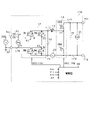
図1に示す電力変換装置100の第1,第2直流側端子TD1,TD2には、不図示の直流電源が接続されており、第1,第2交流側端子TA1,TA2には、交流電源200が接続されている。交流電源200は、例えば商用電源であり、直流電源は、例えばバッテリである。
A DC power supply (not shown) is connected to the first and second DC side terminals TD1 and TD2 of the
電力変換装置100は、コンデンサ16と、ハーフブリッジ回路15と、中間コンデンサ14と、リアクトル13と、フルブリッジ回路12と、第1~第6配線LP1~LP6とを備えている。
The
第1直流側端子TD1には、第1配線LP1の第1端が接続されており、第2直流側端子TD2には第2配線LP2の第1端が接続されている。第1配線LP1と第2配線LP2とは、コンデンサ16により接続されている。
A first end of a first wiring LP1 is connected to the first DC terminal TD1, and a first end of a second wiring LP2 is connected to the second DC terminal TD2. A
第1,第2配線LP1,LP2の第2端には、ハーフブリッジ回路15が接続されている。ハーフブリッジ回路15は、第5スイッチSW5と、第6スイッチSW6とを備えている。第5,第6スイッチSW5,SW6は、電圧駆動型のスイッチであり、本実施形態では、NチャネルMOSFETである。第5スイッチSW5のソースと、第6スイッチSW6のドレインとが接続されている。第5スイッチSW5のドレインが第1配線LP1に接続され、第6スイッチSW6のソースが第2配線LP2に接続されている。本実施形態では、第5スイッチSW5が駆動スイッチに相当する。
A
ハーフブリッジ回路15とフルブリッジ回路12とは、第3配線LP3及び第4配線LP4により接続されている。第3配線LP3の第1端は、第5スイッチSW5のソースと、第6スイッチSW6のドレインとの間の第1接続点K1に接続されている。第3配線LP3には、リアクトル13が設けられている。また、第4配線LP4の第1端は、第6スイッチSW6のソースに接続されている。第3,4配線LP3,LP4それぞれの第2端は、フルブリッジ回路12に接続されている。第3配線LP3と第4配線LP4とは、中間コンデンサ14により接続されている。具体的には、第3配線LP3のうちリアクトル13よりもフルブリッジ回路12側と、第4配線LP4とは、中間コンデンサ14により接続されている。
The
フルブリッジ回路12は、第1~第4スイッチSW1~SW4を備えている。第1~第4スイッチSW1~SW4は、電圧駆動型のスイッチであり、本実施形態では、NチャネルMOSFETである。第1スイッチSW1のソースと、第2スイッチSW2のドレインとが接続されている。第3スイッチSW3のソースと、第4スイッチSW4のドレインとが接続されている。第1,第3スイッチSW1,SW3の各ドレインが第3配線LP3に接続され、第2,第4スイッチSW2,SW4の各ソースが第4配線LP4に接続されている。第1~第4スイッチSW1~SW4それぞれは、逆並列接続された第1~第4ボディーダイオードD1~D4を備えている。
The
第3スイッチSW3のソースと第4スイッチSW4のドレインとの間の第2接続点K2は、第6配線LP6の第1端に接続されており、第6配線LP6の第2端は第2交流側端子TA2に接続されている。第1スイッチSW1と第2スイッチSW2との第3接続点K3は、第5配線LP5の第1端に接続されており、第5配線LP5の第2端は第1交流側端子TA1に接続されている。 A second connection point K2 between the source of the third switch SW3 and the drain of the fourth switch SW4 is connected to the first end of the sixth wiring LP6, and the second end of the sixth wiring LP6 is connected to the second alternating current. It is connected to the side terminal TA2. A third connection point K3 between the first switch SW1 and the second switch SW2 is connected to a first end of the fifth wiring LP5, and a second end of the fifth wiring LP5 is connected to the first AC side terminal TA1. ing.
電力変換装置100は、直流電圧センサ21と、リアクトル電流センサ22と、交流電圧センサ23とを備えている。直流電圧センサ21は、第1,第2配線LP1,LP2の間に接続されており、第1,第2直流側端子TD1,TD2を通じて入力される電圧を直流電圧Vdcとして検出する。リアクトル電流センサ22は、第4配線LP4に設けられており、リアクトル13に流れる電流をリアクトル電流ILrとして検出する。交流電圧センサ23は、第5,第6配線LP5,LP6の間に接続されており、交流電源200の電圧を交流電圧Vacとして検出する。
The
本実施形態では、交流電圧Vacの極性を次のように定めている。第1交流側端子TA1の電圧が第2交流側端子TA2の電圧よりも大きい状態を、交流電圧Vacが正の極性であるとし、第2交流側端子TA2の電圧が第1交流側端子TA1の電圧よりも大きい状態を、交流電圧Vacが負の極性であるとする。 In this embodiment, the polarity of the AC voltage Vac is determined as follows. A state in which the voltage at the first AC-side terminal TA1 is higher than the voltage at the second AC-side terminal TA2 is defined as the AC voltage Vac having a positive polarity, and the voltage at the second AC-side terminal TA2 is higher than that at the first AC-side terminal TA1. Let us assume that the AC voltage Vac is negative in polarity.
電力変換装置100は、第1,第2交流側端子TA1,TA2に流れる電流を出力電流Iacとして検出する出力電流センサ24を備えている。本実施形態では、出力電流センサ24は、第5配線LP5に設けられている。第1交流側端子TA1から交流電源200を介して第2交流側端子TA2の向きに流れる出力電流Iacを正の極性とし、第2交流側端子TA2から交流電源200を介して第1交流側端子TA1の向きに流れる出力電流Iacを負の極性とする。各センサ21~24の検出値は、電力変換装置100の制御装置30に入力される。
The
制御装置30は、第1~第6スイッチSW1~SW6をオンオフ操作する。なお、制御装置30が提供する各機能は、例えば、実体的なメモリ装置に記録されたソフトウェア及びそれを実行するコンピュータ、ハードウェア、又はそれらの組み合わせによって提供することができる。
The
制御装置30は、リアクトル電流センサ22により検出されたリアクトル電流ILrを取得し、取得したリアクトル電流ILrを、交流電圧Vacに基づいて算出した指令電流ILa*に制御すべく、第5,第6スイッチSW5,SW6をオンオフ操作する。本実施形態では、制御装置30は、ピーク電流モード制御により、第5,第6スイッチSW5,SW6をオンオフ操作する。
制御装置30は、交流電圧Vacの極性に基づいて、第1スイッチSW1及び第4スイッチSW4の組と、第2スイッチSW2及び第3スイッチSW3の組とを交互にオン操作する。これにより、交流電圧Vacが正の期間では、第1,第2交流側端子TA1,TA2を介して、交流電源200に正の出力電流Iacが流れる。一方、交流電圧Vacが負の期間では、第1,第2交流側端子TA1,TA2を介して、交流電源200に負の出力電流Iacが流れる。
The
次に、図2を用いて、制御装置30の機能を説明する。制御装置30は、位相推定部31、波形生成部32、乗算器33、絶対値算出部34、加算器35、電流補正部40及び電流制御部50を備えている。本実施形態では、制御装置30が、電流取得部と、交流電圧取得部とに相当する。
Next, the functions of the
位相推定部31は、交流電圧Vacに基づいて、交流電圧Vacの位相θを推定する。この推定方法の一例について説明すると、位相推定部31は、交流電圧Vacの1周期(360°)をカウントし、カウントした値に基づいて位相θを推定する。本実施形態では、交流電圧Vacのゼロアップクロスタイミングをθ=0°とし、交流電圧Vacのゼロダウンクロスタイミングをθ=180°とする。
波形生成部32は、位相推定部31により推定された交流電圧Vacの位相θに基づいて、交流電圧Vacの基準波形sinθを生成する。基準波形sinθは、交流電圧Vacの半周期(T/2)における電圧変化を示す値であり、振幅が1であり、交流電圧Vacと同じ周期で変動する。本実施形態においては、基準波形sinθは、交流電圧Vacと同位相となる。交流電圧Vacが、ゼロクロスタイミングから次のゼロクロスタイミングまで変化する期間が、交流電圧Vacの半周期(T/2)となる。
乗算器33は、リアクトル電流ILrの振幅指令値Ia*と基準波形sinθとを乗算する。振幅指令値Ia*は、リアクトル電流ILrの振幅を定める指令値である。絶対値算出部34は、乗算器33からの出力値の絶対値を、補正前指令電流IL*として設定する。
電流補正部40は、出力電流Iacの歪みを抑制すべく、補正前指令電流IL*に対する補正に用いる電流補正値Icを設定する。本実施形態に係る電流補正部40の構成について図3を用いて説明する。直流電圧を交流電圧に変換する場合、補正前指令電流IL*と、歪みが生じているリアクトル電流ILrの平均値Iaveとの差を示す乖離幅Δiは、ゼロクロスタイミング付近において最も小さな値となる。ここで、乖離幅Δiは、出力電流Iacの歪みの要因となる。乖離幅Δiは、補正前指令電流IL*からリアクトル電流ILrの平均値Iaveを引いた下記式(1)を用いて演算することができる。

上記式(1)により、直流電圧を交流電圧に変換する場合、乖離幅Δiは、交流電圧Vacのゼロクロスタイミングにおいて最小値を取り、交流電圧Vacのピークタイミングにおいて最大値を取る。そのため、上記式(1)により算出される乖離幅Δiに応じて、電流補正値Icを算出することにより、出力電流Iacの歪みを抑制することができる。 When the DC voltage is converted to the AC voltage by the above formula (1), the divergence width Δi takes the minimum value at the zero cross timing of the AC voltage Vac and takes the maximum value at the peak timing of the AC voltage Vac. Therefore, the distortion of the output current Iac can be suppressed by calculating the current correction value Ic according to the divergence width Δi calculated by the above equation (1).
図3に示す電流補正部40は、実効値算出部41と、上限値設定部42と、基準補正値算出部43と、最小値選択部44と、を備えている。実効値算出部41は、交流電圧Vacの実効値Vrmsを算出する。
The
上限値設定部42は、実効値Vrmsと、振幅指令値Ia*とに基づいて上限値Idc設定する。振幅指令値Ia*が大きいほど、リアクトル電流ILrの増加分が大きくなるため、上限値設定部42は、振幅指令値Ia*が大きいほど、上限値Idcを大きな値に設定する。また、実効値Vrmsが大きいほど、第5スイッチSW5のオン期間のデューティ比が大きくなり、乖離幅が増加するため、上限値Idcを大きな値に設定する。
Upper limit
本実施形態では、上限値設定部42は、実効値Vrms毎に、振幅指令値Ia*と、上限値Idcとの関係を示す直流成分マップを備えている。例えば、各実効値Vrmsは、各国の商用電源の実効値Vrmsに対応している。そのため、上限値設定部42は、実効値Vrms毎の直流成分マップを参照することで、振幅指令値Ia*に応じた上限値Idcを設定することができる。
In this embodiment, the upper limit
基準補正値算出部43は、実効値Vrmsに基づいて、基準補正値Ihを設定する。本実施形態では、基準補正値算出部43により設定される基準補正値Ihは、交流電圧Vacのゼロクロスタイミング又はその付近において極小値を取り、ピークタイミングにおいて極大値を取る。具体的には、基準補正値Ihは、時間の推移とともに、その値が変化する。また、本実施形態では、基準補正値Ihは、ゼロクロスタイミングにおいてゼロに定められているが、これに限定されず、ゼロクロスタイミングにおいてゼロより大きい値に定められていても良い。
The reference
基準補正値算出部43は、実効値Vrms毎に、基準補正値Ihを記録した補正値マップを備えている。各補正値マップは、実効値Vrmsが大きいほど、基準補正値Ihが大きな値となるようにその値が定められている。
The reference
最小値選択部44は、上限値設定部42により設定された上限値Idcと、基準補正値算出部43により設定された基準補正値Ihとのうち、小さい方の値を電流補正値Icに設定する。そのため、基準補正値Ihが上限値Idcより小さい値であれば、基準補正値Ihが電流補正値Icとして設定され、基準補正値Ihが上限値Idc以上の値であれば、上限値Idcが電流補正値Icとして設定される。
The minimum
図2の説明に戻り、加算器35は、補正前指令電流IL*に電流補正値Icを加算し、加算後の値を指令電流ILa*として設定する。本実施形態では、指令電流ILa*が電流指令値に相当する。
Returning to the description of FIG. 2, the
電流制御部50は、リアクトル電流センサ22により検出されたリアクトル電流ILrと、指令電流ILa*とに基づいて、第5スイッチSW5を操作する第5ゲート信号GS5と、第6スイッチSW6を操作する第6ゲート信号GS6とを生成する。
Based on the reactor current ILr detected by the
電流制御部50は、DA変換器351と、コンパレータ352と、加算器353と、RSフリップフロップ357と、スロープ補償部60と、を備えている。指令電流ILa*は、DA変換器351に入力される。DA変換器351は、入力された指令電流ILa*をデジタル値からアナログ値に変換する。アナログ値に変換された指令電流ILa*は、コンパレータ352の反転入力端子に入力される。加算器353は、リアクトル電流ILrとスロープ補償部60により設定されたスロープ補償信号Slopeとを加算し、補償したリアクトル電流ILrを出力する。加算器353からの出力は、コンパレータ352の非反転入力端子に入力される。なお、スロープ補償信号Slopeは、リアクトル13に流れる電流の変動に伴う発振を抑制するものである。
The
コンパレータ352は、指令電流ILa*とリアクトル電流ILrとを比較し、リアクトル電流ILrが指令電流ILa*より小さい期間において、ロー状態の信号をRSフリップフロップ357のR端子に入力する。また、コンパレータ352は、リアクトル電流ILrが指令電流ILa*より大きい期間において、ハイ状態の信号をRSフリップフロップ357のR端子に入力する。更に、RSフリップフロップ357のS端子には、クロック信号が入力される。クロック信号の1周期が第5,第6スイッチSW5,SW6の1スイッチング周期Tswとなる。
RSフリップフロップ357のQ端子は、第5スイッチSW5のゲートに接続されている。Q端子から第5スイッチSW5のゲートに出力される信号が、第5ゲート信号GS5となる。また、RSフリップフロップ357の出力端子は、反転器358を介して第6スイッチSW6のゲートに接続されている。Q端子から反転器358を介して第6スイッチSW6のゲートに出力される信号が、第6ゲート信号GS6となる。第6ゲート信号GS6は、第5ゲート信号GS5を反転させた値となる。
A Q terminal of the RS flip-
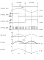
次に、図4を用いて、電力変換装置100の動作を説明する。図4(a)は、交流電圧Vac及び直流電圧Vdcの推移を示している。図4(b)は、第1,第4ゲート信号GS1,GS4の推移を示し、図4(c)は、第2,第3ゲート信号GS2,GS3の推移を示す。図4(d)は、第5ゲート信号GS5と、第6ゲート信号GS6を反転させた信号との推移を示す。図4(e)は、指令電流ILa*の推移を示し、図4(f)は、リアクトル電流ILrの推移を示す。図4(g)は、出力電流Iacの推移を示す。なお、図4において、時刻ta,tc,teは、交流電圧Vacの1周期Tにおいて交流電圧Vacがゼロとなるゼロクロスタイミングである。具体的には、時刻ta,teは交流電圧Vacが負から正に切り替わるゼロアップクロスタイミングであり、時刻tcは交流電圧Vacが正から負に切り替わるゼロダウンクロスタイミングである。また、時刻tbは交流電圧Vacの1周期Tにおける正のピークタイミングであり、時刻tdは交流電圧Vacの1周期Tにおける負のピークタイミングである。
Next, the operation of the
制御装置30は、交流電源200に供給する交流電力の力率を改善するために、交流電圧Vacに基づいて、指令電流ILa*を算出する。そのため、指令電流ILa*は、正弦波の正の半波が周期T/2で繰り返される波形となっている。図4では、指令電流ILa*は、交流電圧Vacのゼロクロスタイミングta,tcから交流電圧Vacのピークタイミングtb,tdに推移するに従い電流が増加する。また、指令電流ILa*は、交流電圧Vacのピークタイミングtb,tdからゼロクロスタイミングtc,teに推移するに従い電流が減少する。
交流電圧Vacの1周期Tにおいて、交流電圧Vacが正となる第1期間P1では、第1,第4ゲート信号GS1,GS4がハイ状態となり、第2,第3ゲート信号GS2,GS3がロー状態となる。これにより、フルブリッジ回路12では、第1,第4スイッチSW1,SW4がオン状態となり、第2,第3スイッチSW2,SW3がオフ状態となる。この第1期間P1において、制御装置30は、ピーク電流モード制御により、リアクトル電流ILrを指令電流ILa*に制御するべく、第5,第6ゲート信号GS5,GS6の1スイッチング周期Tswでのオン期間の比を示すデューティ比(=Ton/Tsw)を変更する。このとき、1スイッチング周期Tswでのリアクトル電流ILrは、第5スイッチのデューティ比に応じた値となる。そのため、リアクトル電流ILrの平均値Iaveは、指令電流ILa*に近い値となる。
In one period T of the AC voltage Vac, in the first period P1 in which the AC voltage Vac is positive, the first and fourth gate signals GS1 and GS4 are in a high state, and the second and third gate signals GS2 and GS3 are in a low state. becomes. As a result, in the
交流電圧Vacが負となる第2期間P2では、第1,第4ゲート信号GS1,GS4がロー状態となり、第2,第3ゲート信号GS2,GS3がハイ状態となる。これにより、フルブリッジ回路12では、第1,第4スイッチSW1,SW4がオフ状態となり、第2,第3スイッチSW2,SW3がオン状態となる。この第2期間P2においても、制御装置30は、ピーク電流モード制御により、リアクトル電流ILrを指令電流ILa*に制御するべく、第5,第6ゲート信号GS5,GS6のデューティ比を変更する。
During the second period P2 in which the AC voltage Vac is negative, the first and fourth gate signals GS1 and GS4 are low, and the second and third gate signals GS2 and GS3 are high. As a result, in the
ここで、交流電源200の実際の交流電圧である実電圧V1の位相に対して、交流電圧センサ23により検出された交流電圧Vacの位相がずれることにより、フルブリッジ回路12を構成する第1~第4スイッチ素子SW1~SW4のオンオフ操作の切り替えタイミングが、実電圧V1の極性が切り替わるタイミングからずれる場合がある。実電圧V1と交流電圧Vacとの間の位相のずれは、例えば、実電圧V1の急な電圧変動や、交流電圧センサ23の検出誤差により生じる。これらの要因によりフルブリッジ回路12内に短絡回路が生じ、第1,第2交流側端子TA1,TA2に過電流が流れる場合がある。
Here, the phase of the AC voltage Vac detected by the
図5,図6を用いて、交流電源200の実電圧V1と交流電圧Vacとの間の位相のずれに起因して過電流が流れる場合について説明する。図5(a)は、交流電圧Vac及び実電圧V1の推移を示し、図5(b)は、第1,第4ゲート信号GS1,GS4の推移を示す。図5(c)は、第2,第3ゲート信号GS2,GS3の推移を示し、図5(d)は、出力電流Iacの推移を示す。図6(a)は、図5の期間P11における、フルブリッジ回路12及び交流電源200に流れる電流を説明する図である。図6(b)は、図5の期間P12における、フルブリッジ回路12及び交流電源200に流れる電流を説明する図である。
A case where an overcurrent flows due to a phase shift between the actual voltage V1 of the
図5(a)で示す交流電圧Vacは、実電圧V1よりも位相が遅れている。これにより、交流電圧Vacが正となる第1期間P1において、第1,第4ゲート信号GS1,GS4の立ち下がりタイミングが、実電圧V1のゼロクロスタイミングよりもΔεだけ遅延している。また、第2,第3ゲート信号GS2,GS3の立ち上がりタイミングが、実電圧V1のゼロクロスタイミングよりもΔεだけ遅延している。更に、期間P11では、実電圧V1が負であるのに対して、交流電圧Vacは正となっている。 The AC voltage Vac shown in FIG. 5(a) is behind the actual voltage V1 in phase. As a result, during the first period P1 in which the AC voltage Vac is positive, the fall timings of the first and fourth gate signals GS1 and GS4 are delayed by Δε from the zero cross timing of the actual voltage V1. Also, the rise timings of the second and third gate signals GS2 and GS3 are delayed by Δε from the zero cross timing of the actual voltage V1. Furthermore, in the period P11, the AC voltage Vac is positive while the actual voltage V1 is negative.
図6(a)に示すように、期間P11では、第1,第2交流側端子TA1,TA2間に印加される負の実電圧V1により、第3スイッチSW3のボディーダイオードD3と、第1スイッチSW1のドレイン・ソース間とを含む閉回路に、第1交流側端子TA1から交流電源200を介して第2交流側端子TA2の向きに、第1電流I1が流れる。同様に、負の実電圧V1により、第4スイッチSW4のドレイン・ソース間と、第2スイッチSW2のボディーダイオードD2とを含む閉回路に、第1交流側端子TA1から交流電源200を介して第2交流側端子TA2の向きに第2電流I2が流れる。そのため、期間P11での出力電流Iacは、第1電流I1と第2電流I2とが足し合わされた過電流となる。
As shown in FIG. 6A, during period P11, the negative actual voltage V1 applied between the first and second AC side terminals TA1 and TA2 causes the body diode D3 of the third switch SW3 and the first switch A first current I1 flows from the first AC side terminal TA1 through the
図5に戻り、期間P12では、第1,第4ゲート信号GS1,GS4の立ち上がりタイミングが、実電圧V1のゼロクロスタイミングよりもΔεだけ遅延している。また、期間P12では、第2,第3ゲート信号GS2,GS3の立ち下がりタイミングが、実電圧V1のゼロクロスタイミングよりもΔεだけ遅延している。更に、期間P12では、実電圧V1が正であるのに対して、交流電圧Vacは負となっている。 Returning to FIG. 5, in the period P12, the rise timings of the first and fourth gate signals GS1 and GS4 are delayed by Δε from the zero cross timing of the actual voltage V1. In period P12, the fall timings of the second and third gate signals GS2 and GS3 are delayed by Δε from the zero crossing timing of the actual voltage V1. Furthermore, in the period P12, the AC voltage Vac is negative while the actual voltage V1 is positive.
図6(b)に示すように、期間P12では、第1,第2交流側端子AT1,AT2間に印加される正の実電圧V1により、第1スイッチSW1のボディーダイオードD1と、第3スイッチSW3のドレイン・ソース間とを含む閉回路に、第2交流側端子TA2から交流電源200を介して第1交流側端子TA1の向きに、第3電流I3が流れる。同様に、正の実電圧V1により、第2スイッチSW2のドレイン・ソース間と、第4スイッチSW4のボディーダイオードD4とを含む閉回路に、第2交流側端子TA2から交流電源200を介して第1交流側端子TA1の向きに第4電流I4が流れる。そのため、期間P12での出力電流Iacは、第3電流I3と第4電流I4とが足し合わされた過電流となる。
As shown in FIG. 6(b), in period P12, the body diode D1 of the first switch SW1 and the third switch SW1 are switched by the positive real voltage V1 applied between the first and second AC side terminals AT1 and AT2. A third current I3 flows from the second AC side terminal TA2 to the first AC side terminal TA1 via the
第1,第2交流側端子TA1,TA2に過電流が流れると、電力変換装置100が安定して動作できなくなるおそれがある。そこで、制御装置30は、出力電流Iacが過電流状態である場合に、過剰な出力電流Iacを低下させるべく、フルブリッジ回路12を形成する第1~第4スイッチSW1~SW4のオンオフ操作を反転させる。詳しくは、図5を参照すると、制御装置30は、期間P11,P12において、第1~第4ゲート信号GS1~GS4のうち、ハイ状態の信号をロー状態に切り換え、ロー状態の信号をハイ状態に切り換える。これにより、交流電圧Vacと実電圧V1との間の位相のずれに起因して第1,第2交流側端子TA1,TA2に過電流が流れるのを抑制することができる。
If overcurrent flows through the first and second AC-side terminals TA1 and TA2, the
制御装置30は、過電流が流れるのを抑制するための構成として、図2に示すように、極性切替部55、反転器359、過電流判定部70及び操作部80を備えている。
As shown in FIG. 2, the
極性切替部55は、推定された位相θに応じて、出力信号の論理を反転させる。本実施形態では、交流電圧Vacのゼロアップクロスタイミングの位相θを0とする。極性切替部55は、0°≦θ<180°の期間においてハイ状態の出力信号を出力する。一方、極性切替部55は、180°≦θ<360°の期間においてロー状態の出力信号を出力する。極性切替部55の出力信号は、反転器359にも入力されており、反転器359により、極性切替部55からの出力信号の論理が反転される。本実施形態では、極性切替部55の出力信号を第1出力信号OUT1と称し、反転器359の出力信号を第2出力信号OUT2と称す。
The
過電流判定部70は、出力電流Iacが過電流状態であるか否かを判定する。操作部80は、第1~第4スイッチSW1~SW4を操作するための第1~第4ゲート信号GS1~GS4を生成する。
過電流判定部70は、極性切替部55から出力された第1出力信号OUT1の論理に応じて過電流閾値TH1を切り換える閾値設定部71と、過電流閾値TH1と出力電流Iacとの比較結果に応じた過電流判定信号DSを出力するコンパレータ72とを備えている。過電流閾値TH1は、過電流状態での出力電流Iacを定めた値であり、本実施形態では、第1~第4スイッチSW1~SW4の定格電流よりも高い値に定められている。
The
図7は、閾値設定部71により出力される過電流閾値TH1を説明する図である。図7(a),(b)に示すように、第1期間P1では、0°≦θ<180°であるため、極性切替部55からの第1出力信号OUT1がハイ状態となり、第2期間P2では、180°≦θ<360°であるため、極性切替部55からの第1出力信号OUT1がロー状態となる。閾値設定部71は、極性切替部55からの第1出力信号OUT1がハイ状態である場合に、正の過電流閾値TH1を出力し、第1出力信号OUT1がロー状態である場合に、負の過電流閾値TH1を出力する。即ち、閾値設定部71は、位相θに応じて交流電圧Vacの極性が変化することから、その極性に応じて、過電流閾値TH1の符号を切り換えている。なお、本実施形態において、正の過電流閾値TH1と負の過電流閾値TH1は、絶対値が同じ値である。
FIG. 7 is a diagram for explaining the overcurrent threshold TH1 output by the
出力電流Iacが過電流状態となった後、下降に転じる際に、出力電流Iacは下降と上昇とを繰り返し、変動が収束するまでには時間を要する。閾値設定部71は、出力電流Iacが過電流状態と判定された後、過電流閾値TH1よりも絶対値が小さな値である解除閾値TH2を設定する。本実施形態では、解除閾値TH2が電流側解除閾値に相当する。出力電流Iacが過電流状態と判定された後、出力電流Iacの絶対値が解除閾値TH2以下になった場合、過電流状態が解除されたと判定される。
After the output current Iac enters an overcurrent state, when it turns to decrease, the output current Iac repeats decrease and increase, and it takes time until the fluctuation converges. After it is determined that the output current Iac is in an overcurrent state, the
図2に戻り、コンパレータ72の一方の入力端子には、出力電流センサ24により検出されたリアクトル電流ILrが入力され、他方の入力端子には、閾値設定部71からの過電流閾値TH1又は解除閾値TH2が入力される。コンパレータ72は、出力電流Iacが過電流閾値TH1よりも大きい場合に、ハイ状態の過電流判定信号DSを出力し、出力電流Iacが過電流閾値TH1以下である場合に、ロー状態の過電流判定信号DSを出力する。また、コンパレータ72は、出力電流Iacが過電流状態と判定された後は、出力電流Iacが解除閾値TH2よりも大きい場合に、ハイ状態の過電流判定信号DSを出力し、出力電流Iacが解除閾値TH2以下である場合に、ロー状態の過電流判定信号DSを出力する。
Returning to FIG. 2, one input terminal of the
操作部80は、補正実行部81と、第1許可判定部82と、第2許可判定部83と、第3許可判定部84と、を備えている。補正実行部81は、極性切替部55から出力される第1出力信号OUT1,及び反転器359から出力される第2出力信号OUT2を補正する。第1~第3許可判定部82~84は、補正実行部81による第1,第2出力信号OUT1,OUT2の補正の可否を判定する。
The
出力電流センサ24により検出された出力電流Iacにノイズが重畳することにより、過電流判定部70が出力電流Iacを過電流状態と誤判定してしまうおそれがある。この場合、第1~第4スイッチSW1~SW4のオンオフ操作を反転させてしまうと、電力変換装置100の動作に悪影響を及ぼすことが懸念される。ここで、交流電圧Vacのゼロクロスタイミング近傍において、実電圧V1と交流電圧Vacとの位相ずれに起因して第1,第2交流側端子TA1,TA2に過電流が流れやすい。第1許可判定部82は、交流電圧Vacの位相θがゼロクロスタイミングの近傍の期間に含まれる場合に、補正実行部81による第1,第2出力信号OUT1,OUT2の補正を許可すべく、ハイ状態の第1許可信号DP1を出力する。一方、第1許可判定部82は、交流電圧Vacの位相θがゼロクロスタイミングの近傍の期間に含まれない場合に、補正実行部81による第1,第2出力信号OUT1,OUT2の補正を禁止すべく、ロー状態の第1許可信号DP1を出力する。
When noise is superimposed on the output current Iac detected by the output
図8を用いて、第1許可信号DP1について説明する。図8(a)は交流電圧Vacの推移を示し、図8(b)は交流電圧Vacの位相θの推移を示し、図8(c)は第1許可信号DP1を示している。第1許可判定部82は、位相推定部31により推定された位相θを監視しており、交流電圧Vacの位相θが補正許可範囲PP1「θ1-X~θ1+X」に含まれていると判定した場合、現在の制御周期が補正許可期間PP1に含まれると判定し、第1許可信号DP1をハイ状態とする。一方、交流電圧Vacの位相θが補正許可範囲PP1に含まれていないと判定した場合、現在の制御周期が補正許可期間PP1に含まれていないと判定し、第1許可信号DP1をロー状態とする。基準となる位相θ1は、交流電圧Vacの1周期Tにおけるゼロクロスタイミング(θ1=0°,180°,360°)である。
The first permission signal DP1 will be described with reference to FIG. 8(a) shows the transition of the AC voltage Vac, FIG. 8(b) shows the transition of the phase θ of the AC voltage Vac, and FIG. 8(c) shows the first permission signal DP1. The first
図9を用いて、第2許可信号DP2について説明する。図9(a)は交流電圧Vacの推移を示し、図9(b)は第2許可信号DP2を示している。補正許可期間PP2は交流電圧Vacのゼロクロスタイミングを含む期間であるため、交流電圧Vacを用いて、補正許可期間PP2を判定することができる。図9(a)では、補正許可期間PP2は、-TH3≦Vac≦TH3となる期間である。電圧閾値TH3は、交流電圧Vacの振幅よりも小さい値である。第2許可判定部83は、取得された交流電圧Vacの絶対値が電圧閾値TH3以下であると判定した場合に、補正実行部81による第1,第2出力信号OUT1,OUT2の補正を許可すべくハイ状態の第2許可信号DP2を出力する。一方、第2許可判定部83は、取得された交流電圧Vacの絶対値が電圧閾値TH3よりも大きいと判定した場合に、補正実行部81による第1,第2出力信号OUT1,OUT2の補正を禁止すべくロー状態の第2許可信号DP2を出力する。
The second permission signal DP2 will be described with reference to FIG. FIG. 9(a) shows transition of the AC voltage Vac, and FIG. 9(b) shows the second permission signal DP2. Since the correction permission period PP2 is a period including the zero-crossing timing of the AC voltage Vac, the correction permission period PP2 can be determined using the AC voltage Vac. In FIG. 9A, the correction permitted period PP2 is a period where −TH3≦Vac≦TH3. Voltage threshold TH3 is a value smaller than the amplitude of AC voltage Vac. The second
続いて、第3許可信号DP3について説明する。電力変換装置100において、フルブリッジ回路12よりも第1,第2直流側端子TD1,TD2側で過電流が流れる場合、リアクトル電流ILrが大きくなることにより、第1,第2交流側端子TA1,TA2に過電流が流れることが懸念される。この場合、第1~第4スイッチSW1~SW4のオンオフ操作を反転させても、出力電流Iacを低減できない可能性が高い。
Next, the third permission signal DP3 will be explained. In the
図10(a)は、リアクトル電流ILrの絶対値の推移を示し、図10(b)は第3許可信号DP3の推移を示している。第3許可判定部84は、リアクトル電流ILrの絶対値を監視している。第3許可判定部84は、リアクトル電流ILrの絶対値が所定のリアクトル電流閾値TH4よりも小さいと判定した場合は、第1,第2出力信号OUT1,OUT2の補正を許可すべくハイ状態の第3許可信号DP3を出力する。一方、第3許可判定部84は、リアクトル電流ILrの絶対値がリアクトル電流閾値TH4以上であると判定した場合に、リアクトル13に過電流が流れていると判定し、第1,第2出力信号OUT1,OUT2の補正を禁止すべくロー状態の第3許可信号DP3を出力する。
FIG. 10(a) shows changes in the absolute value of the reactor current ILr, and FIG. 10(b) shows changes in the third permission signal DP3. Third
図2に戻り、補正実行部81には、極性切替部55からの第1出力信号OUT1、反転器359からの第2出力信号OUT2、過電流判定部70からの過電流判定信号DS、及び第1~第3許可判定部83~85からの第1~第3許可信号DP1~DP3が入力される。補正実行部81の出力部は、第1~第4スイッチSW1~SW4の各ゲートに接続されている。補正実行部81から第1~第4スイッチSW1~SW4の各ゲートに出力される信号が、第1~第4ゲート信号GS1~GS4となる。
Returning to FIG. 2, the correction execution unit 81 includes the first output signal OUT1 from the
補正実行部81は、過電流判定信号DSがロー状態であれば、第1,第2出力信号OUT1,OUT2の論理に応じた第1~第4ゲート信号GS1~GS4を出力する。詳しくは、補正実行部81は、第1出力信号OUT1がハイ状態であれば、ハイ状態の第1,第4ゲート信号GS1,GS4を出力し、第1出力信号OUT1がロー状態であれば、ロー状態の第1,第4ゲート信号GS1,GS4を出力する。また、第2出力信号OUT2がロー状態であれば、ロー状態の第2,第3ゲート信号GS2,GS3を出力し、第2出力信号OUT2がハイ状態であれば、ハイ状態の第2,第3ゲート信号を出力する。 If the overcurrent determination signal DS is low, the correction executing section 81 outputs first to fourth gate signals GS1 to GS4 according to the logic of the first and second output signals OUT1 and OUT2. Specifically, if the first output signal OUT1 is in a high state, the correction execution unit 81 outputs the first and fourth gate signals GS1 and GS4 in a high state, and if the first output signal OUT1 is in a low state, It outputs the first and fourth gate signals GS1 and GS4 in the low state. If the second output signal OUT2 is in a low state, the second and third gate signals GS2 and GS3 in a low state are output. 3 outputs the gate signal.
本実施形態では、第1~第6ゲート信号GS1~GS6がハイ状態となることにより、第1~第6スイッチSW1~SW6は、フルオン状態となる。なお、フルオン状態は、スイッチのゲート電圧が閾値電圧以上となってスイッチのオン状態が維持されつつ、スイッチのオン抵抗が略ゼロとなる状態である。 In the present embodiment, the first to sixth gate signals GS1 to GS6 are in a high state, so that the first to sixth switches SW1 to SW6 are in a full on state. Note that the full-on state is a state in which the on-resistance of the switch becomes substantially zero while the gate voltage of the switch becomes equal to or higher than the threshold voltage and the on-state of the switch is maintained.
補正実行部81は、過電流判定信号DSがハイ状態であっても、第1~第3許可信号DP1~DP3の少なくとも1つがロー状態であれば、上述したように、第1,第2出力信号OUT1,OUT2の論理に応じた第1~第4ゲート信号GS1~GS4を出力する。 Even if the overcurrent determination signal DS is high, if at least one of the first to third permission signals DP1 to DP3 is low, the correction execution unit 81 performs the first and second outputs as described above. It outputs the first to fourth gate signals GS1 to GS4 according to the logic of the signals OUT1 and OUT2.
補正実行部81は、過電流判定信号DSがハイ状態であって、かつ第1~第3許可信号DP1~DP3の全てがハイ状態であれば、第1,第2出力信号OUT1,OUT2の論理を反転させた値に応じた第1~第4ゲート信号GS1~GS4を出力する。詳しくは、補正実行部81は、第1出力信号OUT1がハイ状態であれば、ロー状態の第1,第4ゲート信号GS1,GS4を出力し、第1出力信号OUT1がロー状態であれば、ハイ状態の第1,第4ゲート信号GS1,GS4を出力する。また、補正実行部81は、第2出力信号OUT2がロー状態であれば、ハイ状態の第2,第3ゲート信号GS2,GS3を出力し、第2出力信号OUT2がハイ状態であれば、ロー状態の第2,第3ゲート信号GS2,GS3を出力する。これにより、出力電流Iacが過電流状態と判定されている期間において、第1,第4スイッチSW1,SW4の組と、第2,第3スイッチSW2,SW3の組とのオンオフ操作が反転される。 If the overcurrent determination signal DS is in a high state and all of the first to third permission signals DP1 to DP3 are in a high state, the correction execution unit 81 outputs the logic values of the first and second output signals OUT1 and OUT2. , and outputs the first to fourth gate signals GS1 to GS4 corresponding to the inverted values of . Specifically, if the first output signal OUT1 is in a high state, the correction execution unit 81 outputs the first and fourth gate signals GS1 and GS4 in a low state, and if the first output signal OUT1 is in a low state, It outputs the first and fourth gate signals GS1 and GS4 in a high state. Further, the correction execution unit 81 outputs the second and third gate signals GS2 and GS3 in the high state when the second output signal OUT2 is in the low state, and outputs the second and third gate signals GS2 and GS3 in the high state when the second output signal OUT2 is in the high state. state second and third gate signals GS2 and GS3. As a result, the ON/OFF operation of the set of the first and fourth switches SW1 and SW4 and the set of the second and third switches SW2 and SW3 is reversed during the period in which the output current Iac is determined to be in the overcurrent state. .
次に、本実施形態に係るピーク電流モード制御を用いた第1~第6スイッチSW1~SW6の操作手順を、図11を用いて説明する。図11に示す処理は、制御装置30により所定の制御周期で繰り返し実施される。
Next, a procedure for operating the first to sixth switches SW1 to SW6 using peak current mode control according to this embodiment will be described with reference to FIG. The processing shown in FIG. 11 is repeatedly performed by the
ステップS11では、補正前指令電流IL*を算出する。ステップS12では、交流電圧Vacに基づいて、電流補正値Icを設定する。ステップS13では、電流補正値Icにより補正前指令電流IL*を補正した値を指令電流ILa*として算出する。 In step S11, pre-correction command current IL* is calculated. In step S12, a current correction value Ic is set based on the AC voltage Vac. In step S13, a value obtained by correcting the pre-correction command current IL* using the current correction value Ic is calculated as the command current ILa*.
ステップS14では、ステップS13で算出した指令電流ILa*を用いたピーク電流モード制御により、第5,第6ゲート信号GS5,GS6を出力する。 At step S14, fifth and sixth gate signals GS5 and GS6 are output by peak current mode control using the command current ILa* calculated at step S13.
ステップS15では、交流電圧Vacの極性が正であるか否かを判定する。交流電圧Vacの極性が正であると判定すると、ステップS16に進み、第1出力信号OUT1をハイ状態に設定し、第2出力信号OUT2をロー状態に設定する。一方、交流電圧Vacの極性が負であると判定すると、ステップS17に進み、第1出力信号OUT1をロー状態に設定し、第2出力信号OUT2をハイ状態に設定する。 In step S15, it is determined whether the polarity of the AC voltage Vac is positive. When it is determined that the polarity of the AC voltage Vac is positive, the process advances to step S16 to set the first output signal OUT1 to a high state and the second output signal OUT2 to a low state. On the other hand, if it is determined that the polarity of the AC voltage Vac is negative, the process advances to step S17 to set the first output signal OUT1 to the low state and the second output signal OUT2 to the high state.
ステップS18では、第1,第2出力信号OUT1,OUT2に対する補正許可判定を行う。具体的には、第1~第3許可信号DP1~DP3の全てがハイ状態であると判定すると、第1,第2出力信号OUT1,OUT2の補正を許可し、ステップS19に進む。一方、第1~第3許可信号DP1~DP3の少なくとも1つがロー状態であると判定すると、第1,第2出力信号OUT1,OUT2の補正を禁止し、ステップS25に進む。ステップS25では、第1,第2出力信号OUT1,OUT2を反転させることなく、第1~第4スイッチSW1~SW4に出力する。これにより、交流電圧Vacの極性に応じてステップS16又はステップS17で設定した第1出力信号OUT1の論理に応じた第1,第4ゲート信号GS1,GS4が第1,第4スイッチSW1,SW4に出力され、同様にステップS16又はステップS17で設定した第2出力信号OUT2の論理に応じた第2,第3ゲート信号GS2,GS3が第2,第3スイッチSW2,SW3に出力される。そして、図11の処理を一旦終了する。 In step S18, it is determined whether correction is permitted for the first and second output signals OUT1 and OUT2. Specifically, when it is determined that all of the first to third permission signals DP1 to DP3 are in the high state, correction of the first and second output signals OUT1 and OUT2 is permitted, and the process proceeds to step S19. On the other hand, if it is determined that at least one of the first to third permission signals DP1 to DP3 is in the low state, correction of the first and second output signals OUT1 and OUT2 is prohibited, and the process proceeds to step S25. In step S25, the first and second output signals OUT1 and OUT2 are output to the first to fourth switches SW1 to SW4 without being inverted. As a result, the first and fourth gate signals GS1 and GS4 corresponding to the logic of the first output signal OUT1 set in step S16 or step S17 according to the polarity of the AC voltage Vac are applied to the first and fourth switches SW1 and SW4. Similarly, the second and third gate signals GS2 and GS3 corresponding to the logic of the second output signal OUT2 set in step S16 or step S17 are output to the second and third switches SW2 and SW3. Then, the process of FIG. 11 is temporarily terminated.
ステップS19では、出力電流Iacの絶対値が過電流閾値TH1よりも大きいか否かを判定する。出力電流Iacの絶対値が過電流閾値TH1よりも大きいと判定すると、ステップS20に進み、出力電流Iacが過電流状態であることを示す過電流判定フラグFをハイ状態とする。そして、ステップS24に進み、第1出力信号OUT1及び第2出力信号OUT2の論理を反転させる。具体的には、ステップS16において設定した第1出力信号OUT1をロー状態に切り替え、第2出力信号OUT2をハイ状態に切り替える。または、ステップS17において設定した第1出力信号OUT1をハイ状態に切り替え、第2出力信号OUT2をロー状態に切り替える。これにより、第1出力信号OUT1により定まる第1,第4ゲート信号GS1,GS4が反転し、第2出力信号OUT2により定まる第2,第3ゲート信号GS2,GS3が反転する。 In step S19, it is determined whether or not the absolute value of the output current Iac is greater than the overcurrent threshold TH1. When it is determined that the absolute value of the output current Iac is greater than the overcurrent threshold TH1, the process proceeds to step S20 to set the overcurrent determination flag F, which indicates that the output current Iac is in an overcurrent state, to a high state. Then, in step S24, the logics of the first output signal OUT1 and the second output signal OUT2 are inverted. Specifically, the first output signal OUT1 set in step S16 is switched to the low state, and the second output signal OUT2 is switched to the high state. Alternatively, the first output signal OUT1 set in step S17 is switched to a high state, and the second output signal OUT2 is switched to a low state. As a result, the first and fourth gate signals GS1 and GS4 determined by the first output signal OUT1 are inverted, and the second and third gate signals GS2 and GS3 determined by the second output signal OUT2 are inverted.
ステップS19において出力電流Iacの絶対値が過電流閾値TH1以下であると判定すると、ステップS21に進み、過電流判定フラグFがハイ状態となっているか否かを判定する。過電流判定フラグFがロー状態であると判定すると、ステップS25に進む。一方、出力電流Iacを過電流状態であると判定している場合、ステップS21において過電流判定フラグFがハイ状態であると判定され、ステップS22に進み、過電流状態が解消したか否かを判定する。具合的には、ステップS22では、出力電流Iacの絶対値が解除閾値TH2以下か否かを判定する。出力電流Iacの絶対値が解除閾値TH2よりも大きいと判定すると、ステップS24に進む。この場合、過電流状態の判定を継続する。出力電流Iacの絶対値が解除閾値TH2以下であると判定すると、ステップS23に進み、過電流判定フラグFをロー状態とする。即ち、過電流状態の判定を解除する。 If it is determined in step S19 that the absolute value of the output current Iac is equal to or less than the overcurrent threshold TH1, the process proceeds to step S21 to determine whether or not the overcurrent determination flag F is in a high state. If it is determined that the overcurrent determination flag F is low, the process proceeds to step S25. On the other hand, when it is determined that the output current Iac is in an overcurrent state, it is determined in step S21 that the overcurrent determination flag F is in a high state, and the process proceeds to step S22 to determine whether or not the overcurrent state has been resolved. judge. Specifically, in step S22, it is determined whether or not the absolute value of the output current Iac is equal to or less than the release threshold TH2. If it is determined that the absolute value of the output current Iac is greater than the release threshold TH2, the process proceeds to step S24. In this case, the determination of the overcurrent state is continued. If it is determined that the absolute value of the output current Iac is equal to or less than the release threshold TH2, the process proceeds to step S23, and the overcurrent determination flag F is set to low. That is, the determination of the overcurrent state is canceled.
次に、図12を用いて、制御装置30の処理について説明する。図12(a)は実電圧V1及び交流電圧Vacの推移を示し、図12(b)は第1,第4ゲート信号GS1,GS4の推移を示し、図12(c)は第2,第3ゲート信号GS2,GS3の推移を示し、図12(d)は出力電流Iacの推移を示す。
Next, processing of the
実電圧V1と交流電圧Vacとの間で位相のずれが生じることにより、時刻t1以降において実電圧V1が正であるのに交流電圧Vacが負となる期間が生じる。そのため、フルブリッジ回路12内に短絡回路が生じ、第1,第2交流側端子TA1,TA2に流れる負の出力電流Iacが増加する。
Due to the phase shift between the actual voltage V1 and the AC voltage Vac, there occurs a period after time t1 in which the AC voltage Vac is negative while the actual voltage V1 is positive. Therefore, a short circuit occurs in the
時刻t2において、出力電流Iacの絶対値が過電流閾値TH1よりも大きくなることにより、第1,第4ゲート信号GS1,GS4がロー状態からハイ状態に切り替えられ、第2,第3ゲート信号GS2,GS3がハイ状態からロー状態に切り替えられる。これにより、負の出力電流Iacの増加が抑制され、第1,第2交流側端子TA1,TA2の過電流状態が解消される。なお、図12(b),(c)では、破線にて、制御装置30により第1~第4ゲート信号GS1~GS4の切り替えが実施されないと想定した場合の第1~第4ゲート信号GS1~GS4を示す。
At time t2, the absolute value of the output current Iac becomes greater than the overcurrent threshold TH1, so that the first and fourth gate signals GS1 and GS4 are switched from low to high, and the second and third gate signals GS2 , GS3 are switched from the high state to the low state. As a result, an increase in the negative output current Iac is suppressed, and the overcurrent state of the first and second AC side terminals TA1 and TA2 is eliminated. In FIGS. 12(b) and 12(c), the dashed lines indicate the first to fourth gate signals GS1 to GS4 when it is assumed that the
時刻t3では、交流電圧Vacの極性が負から正に変化することにより、交流電圧Vacと実電圧V1との極性が一致する。これにより、フルブリッジ回路12内には短絡回路が生じない。交流電圧Vac及び実電圧V1が正となる期間では、第1,第2交流側端子TA1,TA2に正の出力電流Iacが流れる。
At time t3, the polarity of AC voltage Vac changes from negative to positive, so that the polarities of AC voltage Vac and actual voltage V1 match. Thereby, no short circuit occurs in the
時刻t4では、実電圧V1の極性が正から負に変化することにより、交流電圧Vacと実電圧V1との極性が不一致となる。これにより、フルブリッジ回路12に短絡回路が生じ、第1,第2交流側端子TA1,TA2に流れる正の出力電流Iacが増加する。
At time t4, the polarity of the actual voltage V1 changes from positive to negative, so that the polarities of the AC voltage Vac and the actual voltage V1 do not match. As a result, a short circuit occurs in the
時刻t5で、出力電流Iacの絶対値が過電流閾値TH1よりも大きくなることにより、第1,第4ゲート信号GS1,GS4がハイ状態からロー状態に切り替えられ、第2,第3ゲート信号GS2,GS3がロー状態からハイ状態に切り替えられる。これにより、正の出力電流Iacが低下し、過電流状態が解消される。なお、時刻t6で、交流電圧Vacの極性が正から負に変化することにより、交流電圧Vacと実電圧V1との極性が一致するため、フルブリッジ回路12内に短絡回路が生じなくなる。 At time t5, the absolute value of the output current Iac becomes larger than the overcurrent threshold TH1, so that the first and fourth gate signals GS1 and GS4 are switched from high to low, and the second and third gate signals GS2 , GS3 are switched from the low state to the high state. This reduces the positive output current Iac and eliminates the overcurrent condition. At time t6, the polarity of the AC voltage Vac changes from positive to negative, so that the polarities of the AC voltage Vac and the actual voltage V1 match.
続いて、先の図3で説明した基準補正値マップの作成方法について図13を用いて説明する。 Next, a method for creating the reference correction value map described with reference to FIG. 3 will be described with reference to FIG.
本実施形態では、乖離幅Δiを、補正前指令電流IL*からリアクトル電流ILrの平均値Iaveを引いた値としている。なお、図13において、Dは、第5スイッチSW5におけるオン期間のデューティ比を示す。 In the present embodiment, the divergence width Δi is a value obtained by subtracting the average value Iave of the reactor current ILr from the pre-correction command current IL*. In FIG. 13, D indicates the duty ratio of the ON period of the fifth switch SW5.
図13より、乖離幅Δiは、オン期間(=D×Tsw)でのスロープ補償信号Slopeの最大増加分Δslopeに、リアクトル電流ILrの最大増加分ΔILの半分の値(ΔIL/2)を加えたものとみなすことができる。そのため、乖離幅Δiは、下記数式(1)により算出される。 From FIG. 13, the divergence width Δi is obtained by adding half the maximum increase ΔIL of the reactor current ILr (ΔIL/2) to the maximum increase Δslope of the slope compensation signal Slope during the ON period (=D×Tsw). can be regarded as Therefore, the divergence width Δi is calculated by the following formula (1).
Δi=IL*-Iave=Δslope+ΔIL/2 … (2)
また、リアクトル電流ILrの最大増加分ΔILは、リアクトル13の両端に生じる電圧と、リアクトル13のインダクタンスLとを用いて、下記式(3)により算出することができる。
Δi=IL*−Iave=Δslope+ΔIL/2 (2)
Also, the maximum increase ΔIL of the reactor current ILr can be calculated by the following equation (3) using the voltage generated across the

Δslope = ms×D×Tsw … (4)
例えば、乖離幅Δiを算出する際のスロープ補償信号Slopeの傾きmsは、傾きmsの平均値を用いればよい。
Δslope=ms×D×Tsw (4)
For example, the average value of the slope ms may be used as the slope ms of the slope compensation signal Slope when calculating the divergence width Δi.
第5スイッチSW5のオン期間のデューティ比Dは、交流電圧acの実効値Vrmsを用いて、下記式(5)により算出することができる。 The duty ratio D of the ON period of the fifth switch SW5 can be calculated by the following formula (5) using the effective value Vrms of the AC voltage ac.

以上説明した本実施形態では、以下の効果を奏することができる。 In the embodiment described above, the following effects can be obtained.
・制御装置30は、第1,第2交流側端子TA1,TA2に流れる出力電流Iacが過電流状態であるか否かを判定する。制御装置30は、過電流状態であると判定した場合に、第1~第4スイッチSW1~SW4のオンオフ操作を反転させる。これにより、交流電源200の急な電圧変動や、交流電圧センサ23の検出誤差に起因して、交流電圧Vacと実電圧V1との間に位相のずれが生じる場合でも、第1,第2交流側端子TA1,TA2に過剰な出力電流Iacが流れるのが抑制される。また、交流電圧Vacと実電圧V1との間の位相のずれが解消した後は、第1~第4スイッチSW1~SW4のオンオフ操作の反転が行われなくなることにより、電力変換装置100の動作を継続させることができる。
- The
・制御装置30は、過電流状態であると判定した場合に、第1,第4スイッチSW1,SW4の組と、第2,第3スイッチSW2,SW3の組とのうち、オン操作されているスイッチの組をオフ操作に切り替え、残りのスイッチの組をオン操作に切り替える。これにより、第1,第4スイッチSW1,SW4の組と、第2,第3スイッチSW2,SW3の組との間のオンオフ操作の切り換えタイミングのずれが解消され、第1,第2交流側端子TA1,TA2に過電流が流れるのをいっそう抑制することができる。
When the
・制御装置30は、出力電流Iacの絶対値が過電流閾値TH1よりも大きい場合に、過電流状態であると判定する。その後、制御装置30は、出力電流Iacの絶対値が、過電流閾値TH1よりも小さい解除閾値TH2以下であると判定した場合に、出力電流Iacの過電流状態が解消されたと判定する。これにより、出力電流Iacが上昇から下降に転じた際に出力電流Iacの変動により、再度、過電流状態であると判定されることが抑制され、第1~第4スイッチSW1~SW4のオンオフ操作が不要に切り換えられるのを防止することができる。
- The
・制御装置30は、位相θが、交流電圧Vacのゼロクロスタイミング近傍の期間であることを条件に、第1,第4スイッチSW1,SW4の組と、第2,第3スイッチSW2,SW3の組とのオンオフ操作を反転させる。これにより、ノイズ等の影響によって過電流状態であることを誤判定した場合でも、第1~第4スイッチSW1~SW4のオンオフ操作を反転させてしまうのを抑制することができる。
The
・制御装置30は、交流電圧Vacの絶対値が所定の電圧閾値TH3よりも小さいことを条件に、第1,第4スイッチSW1,SW4の組と、第2,第3スイッチSW2,SW3の組とのオンオフ操作を反転させる。これにより、ノイズ等の影響によって過電流状態であることを誤判定した場合でも、第1~第4スイッチSW1~SW4のオンオフ操作を反転させてしまうのを抑制することができる。
The
・制御装置30は、リアクトル電流ILrの絶対値がリアクトル電流閾値TH4よりも小さいことを条件に、第1,第4スイッチSW1,SW4の組と、第2,第3スイッチSW2,SW3の組とのオンオフ操作を反転させる。これにより、交流電源200の急な電圧変動や、交流電圧センサ23の検出誤差に起因する過剰な出力電流のみを抑制することができる。
The
<第1実施形態の変形例1>
制御装置30は、過電流状態であると判定している場合に、第1,第4スイッチSW1,SW4の組と、第2,第3スイッチSW2,SW3の組とのうち、オン操作されている組のみをオフ操作に切り換えてもよい。例えば、図6(a)で示したフルブリッジ回路12内に形成された短絡回路のうち、第1,第4スイッチSW1,SW4がオン操作からオフ操作に切り替わることにより、第1電流I1が流れる短絡回路が形成されなくなる。これにより、第1,第2交流側端子TA1,TA2に流れる出力電流が減少し、過電流状態が緩和される。
<
When the
<第2実施形態>
第2実施形態では、第1実施形態と異なる構成を主に説明する。なお、第1実施形態と同一の符号を付した構成は同一の構成を示し、その説明は繰り返さない。
<Second embodiment>
2nd Embodiment mainly demonstrates a different structure from 1st Embodiment. In addition, the structure which attached|subjected the code|symbol same as 1st Embodiment shows the same structure, and the description is not repeated.
ピーク電流モード制御では、指令電流ILa*に応じた出力電流Iacが流れるため、出力電流Iacが過電流状態になっていなければ、出力電流Iacと指令電流ILa*との偏差は相対的に小さくなる。一方、出力電流Iacが過電流状態になっていれば、出力電流Iacと指令電流ILa*との偏差は相対的に大きくなる。 In the peak current mode control, the output current Iac flows according to the command current ILa*. Therefore, unless the output current Iac is in an overcurrent state, the deviation between the output current Iac and the command current ILa* becomes relatively small. . On the other hand, if output current Iac is in an overcurrent state, the deviation between output current Iac and command current ILa* becomes relatively large.
本実施形態では、過電流判定部70は、出力電流Iacの絶対値と指令電流ILa*との差の絶対値が偏差閾値TH5よりも大きい場合に、過電流状態であると判定する。図14は、本実施形態に係る第1~第6スイッチの操作手順を説明するフローチャートである。図14に示す処理は、制御装置30により所定の制御周期で繰り返し実施される。
In this embodiment, the
ステップS18において、第1~第3許可信号DP1~DP3の全てがハイ状態であると判定すると、ステップS30に進む。ステップS30では、出力電流Iacの絶対値と指令電流ILa*との差の絶対値が偏差閾値TH5よりも大きいか否かを判定する。ステップS30において肯定判定すると、ステップS20に進み、過電流判定フラグFをハイ状態に設定する。一方、ステップS30において否定判定すると、ステップS21に進む。 If it is determined in step S18 that all of the first to third permission signals DP1 to DP3 are in a high state, the process proceeds to step S30. In step S30, it is determined whether or not the absolute value of the difference between the absolute value of the output current Iac and the command current ILa* is greater than the deviation threshold TH5. If an affirmative determination is made in step S30, the process proceeds to step S20 to set the overcurrent determination flag F to a high state. On the other hand, if a negative determination is made in step S30, the process proceeds to step S21.
本実施形態においても、出力電流Iacの絶対値と指令電流ILa*との偏差を用いて、過電流状態であると判定した後に、ヒステリシスを考慮して過電流状態の判定からの解除条件を定めている。具体的には、図14のステップS30で否定判定して、ステップS31に進む場合、出力電流Iacの絶対値と指令電流ILa*との差の絶対値が、偏差閾値TH5よりも小さい値である偏差側解除閾値TH6以下であるか否かを判定する。ステップS31で肯定判定すると、ステップS23に進み、過電流判定フラグFをロー状態に設定する。一方、ステップS31で否定判定すると、ステップS24に進み、過電流状態の判定を継続する。 In the present embodiment as well, the deviation between the absolute value of the output current Iac and the command current ILa* is used to determine the overcurrent state, and then the condition for canceling the determination of the overcurrent state is determined in consideration of the hysteresis. ing. Specifically, when a negative determination is made in step S30 of FIG. 14 and the process proceeds to step S31, the absolute value of the difference between the absolute value of the output current Iac and the command current ILa* is a value smaller than the deviation threshold TH5. It is determined whether or not the difference is equal to or less than the deviation side cancellation threshold TH6. If an affirmative determination is made in step S31, the process proceeds to step S23 to set the overcurrent determination flag F to a low state. On the other hand, if a negative determination is made in step S31, the process proceeds to step S24 to continue determination of the overcurrent state.
以上説明した本実施形態では、指令電流ILa*を基準として、出力電流Iacが過電流状態であるか否かを判定することができるため、出力電流Iacが低い値である場合でも、出力電流Iacが過電流状態であるか否かを適正に判定することができる。 In the present embodiment described above, it is possible to determine whether or not the output current Iac is in an overcurrent state based on the command current ILa*. is in an overcurrent state.
<第3実施形態>
第3実施形態では、第1実施形態と異なる構成を主に説明する。なお、第1実施形態と同一の符号を付した構成は同一の構成を示し、その説明は繰り返さない。
<Third Embodiment>
3rd Embodiment mainly demonstrates a different structure from 1st Embodiment. In addition, the structure which attached|subjected the code|symbol same as 1st Embodiment shows the same structure, and the description is not repeated.
電力変換装置100では、第1,第4スイッチSW1,SW4の組がオン操作される期間において、正の出力電流Iacが流れ、第2,第3スイッチSW2,SW3の組がオン操作される期間において、負の出力電流Iacが流れる。本実施形態では、制御装置30は、出力電流Iacが正となる正の過電流状態を判定した場合に、第1,第4スイッチSW1,SW4がオン操作される期間であることを条件に、第1~第4スイッチSW1~SW4の操作をオン操作からオフ操作に反転させる。また、制御装置30は、出力電流Iacが負となる負の過電流状態であると判定した場合に、第2,第3スイッチSW2,SW3がオン操作される期間であることを条件に、第2,第3スイッチSW2,SW3の操作をオン操作からオフ操作に反転させる。
In the
図15は、本実施形態に係る第1~第6スイッチの操作手順を説明するフローチャートである。図15に示す処理は、制御装置30により所定の制御周期で繰り返し実施される。図15に示す処理では、先の図11に示した処理のステップS18,S19に代えて、ステップS40~S42が設けられている。
FIG. 15 is a flow chart for explaining the operation procedure of the first to sixth switches according to this embodiment. The processing shown in FIG. 15 is repeatedly performed by the
ステップS16又はステップS17において、交流電圧Vacの極性に応じて、第1,第2出力信号OUT1,OUT2の論理を切り換えると、ステップS40に進む。ステップS40では、第1,第4スイッチSW1,SW4がオン操作される期間であるか否かを判定する。例えば、第1出力信号OUT1の論理がハイ状態である場合に、第1,第4スイッチSW1,SW4がオン操作される期間であると判定する。ステップS40を肯定判定した場合、ステップS41に進む。 After switching the logic of the first and second output signals OUT1 and OUT2 in step S16 or S17 according to the polarity of the AC voltage Vac, the process proceeds to step S40. In step S40, it is determined whether or not the first and fourth switches SW1 and SW4 are being turned on. For example, when the logic of the first output signal OUT1 is in a high state, it is determined that it is a period in which the first and fourth switches SW1 and SW4 are turned on. If the determination in step S40 is affirmative, the process proceeds to step S41.
ステップS41では、出力電流Iacが正の過電流状態であるか否かを判定する。具体的には、出力電流Iacが過電流閾値TH1よりも大きい場合に、出力電流Iacが正の過電流状態であると判定する。そして、ステップS20に進み、過電流判定フラグFをハイ状態に設定する。一方、出力電流Iacが過電流閾値TH1以下である場合、出力電流Iacが過電流状態でないとして、ステップS21に進む。 In step S41, it is determined whether or not the output current Iac is in a positive overcurrent state. Specifically, when the output current Iac is greater than the overcurrent threshold TH1, it is determined that the output current Iac is in a positive overcurrent state. Then, in step S20, the overcurrent determination flag F is set to a high state. On the other hand, if the output current Iac is equal to or less than the overcurrent threshold TH1, it is determined that the output current Iac is not in an overcurrent state, and the process proceeds to step S21.
ステップS40を否定判定した場合、第2,第3スイッチSW2,SW3がオン操作される期間であるため、ステップS42では、出力電流Iacが負の過電流状態であるか否かを判定する。具体的には、出力電流Iacが過電流閾値TH1の符号を負とした値(=-TH1)よりも小さい場合に、出力電流Iacが負の過電流状態であると判定する。そして、ステップS20に進み、過電流判定フラグFをハイ状態に設定する。一方、ステップS42を否定判定する場合、ステップS21に進む。 If a negative determination is made in step S40, it is a period in which the second and third switches SW2 and SW3 are turned on, so in step S42 it is determined whether or not the output current Iac is in a negative overcurrent state. Specifically, when the output current Iac is smaller than the negative value (=-TH1) of the overcurrent threshold TH1, it is determined that the output current Iac is in the negative overcurrent state. Then, in step S20, the overcurrent determination flag F is set to a high state. On the other hand, if a negative determination is made in step S42, the process proceeds to step S21.
以上説明した第3実施形態では、第1実施形態と同様の効果を奏することができる。 In the third embodiment described above, the same effects as in the first embodiment can be obtained.
<第4実施形態>
第4実施形態では、第1実施形態と異なる構成を主に説明する。なお、第1実施形態と同一の符号を付した構成は同一の構成を示し、その説明は繰り返さない。
<Fourth Embodiment>
4th Embodiment mainly demonstrates a different structure from 1st Embodiment. In addition, the structure which attached|subjected the code|symbol same as 1st Embodiment shows the same structure, and the description is not repeated.
電力変換装置100において、フルブリッジ回路12よりも第1,第2直流側端子TD1,TD2側で過電流が流れる場合、リアクトル電流ILrが大きくなることにより、リアクトル電流ILrと指令電流ILa*との差の絶対値が大きくなる。一方で、交流電圧Vacと実電圧V1との間の位相がずれることにより過剰な出力電流Iacが流れる場合、リアクトル電流ILrと指令電流ILa*との差の絶対値は大きな値とならない。本実施形態では、制御装置30は、リアクトル電流ILrと指令電流ILa*との差の絶対値が所定の電流差閾値TH7よりも小さいことを条件に、第1~第4スイッチSW1~SW4のオンオフ操作を反転させる。
In the
図16は、本実施形態に係る第1~第6スイッチの操作手順を説明するフローチャートである。図16に示す処理は、制御装置30により所定の制御周期で繰り返し実施される。
FIG. 16 is a flow chart for explaining the operation procedure of the first to sixth switches according to this embodiment. The processing shown in FIG. 16 is repeatedly performed by the
ステップS50では、リアクトル電流ILrと指令電流ILa*との差の絶対値が電流差閾値TH7よりも小さいか否かを判定する。ステップS50で肯定判定する場合、フルブリッジ回路12よりも第1,第2直流側端子TD1,TD2側で過電流が流れていないため、ステップS19に進む。一方、ステップS50で否定判定する場合、フルブリッジ回路12よりも第1,第2直流側端子TD1,TD2側で過電流が流れているため、ステップS25に進む。
In step S50, it is determined whether or not the absolute value of the difference between the reactor current ILr and the command current ILa* is smaller than the current difference threshold TH7. If an affirmative determination is made in step S50, no overcurrent is flowing on the side of the first and second DC terminals TD1 and TD2 of the
以上説明した本実施形態では、第1実施形態と同様の効果を奏することができる。 The present embodiment described above can achieve the same effects as those of the first embodiment.
<第5実施形態>
第5実施形態では、第1実施形態と異なる構成を主に説明する。なお、第1実施形態と同一の符号を付した構成は同一の構成を示し、その説明は繰り返さない。
<Fifth Embodiment>
5th Embodiment mainly demonstrates a different structure from 1st Embodiment. In addition, the structure which attached|subjected the code|symbol same as 1st Embodiment shows the same structure, and the description is not repeated.
本実施形態では、制御装置30は、過電流状態であると判定している期間に渡って、第1~第4スイッチSW1~SW4の全てをオフ操作することにより、過剰な出力電流Iacを低減する。具体的には、制御装置30は、過電流状態であると判定している期間に渡って、第1,第4スイッチSW1,SW4の組と、第2,第3スイッチSW2,SW3の組とのうち、オン操作されているスイッチの組のみをオフ操作に切り替える。
In this embodiment, the
図17に示すように、本実施形態に係る制御装置30では、RSフリップフロップ357のQ端子からの出力及び反転器358からの出力は、操作部80の補正実行部81に入力される。本実施形態では、補正実行部81の出力は、第1~第4スイッチSW1~SW4の各ゲートに加えて、第5,第6スイッチSW5,SW5の各ゲートに接続されている。補正実行部81から第5スイッチSW5のゲートに出力される信号が、第5ゲート信号GS5となり、補正実行部81から第6スイッチSW6のゲートに出力される信号が、第6ゲート信号GS6となる。以下では、RSフリップフロップ357のQ端子から補正実行部81に出力される信号を、第3出力信号OUT3と称し、反転器358から補正実行部81に出力される信号を、第4出力信号OUT4と称する。
As shown in FIG. 17 , in the
補正実行部81は、過電流判定信号DSがハイ状態であって、かつ第1~第3許可信号DP1~DP3のすべてがハイ状態であれば、第1,第2出力信号OUT1,OUT2のうち、ハイ状態の出力信号の論理をロー状態に反転させる。この場合、補正実行部81は、第1出力信号OUT1がハイ状態であれば、第1出力信号OUT1の論理を反転させることにより、第1,第4ゲート信号GS1,GS4をロー状態にする。また、補正実行部81は、第2出力信号OUT2がハイ状態であれば、第2出力信号OUT2の論理を反転させることにより、第2,第3ゲート信号GS2,GS3をロー状態にする。これにより、過電流状態であると判定されている期間において、第1~第4ゲート信号GS1~GS4の全てがロー状態に維持される。 If the overcurrent determination signal DS is in a high state and all of the first to third permission signals DP1 to DP3 are in a high state, the correction execution unit 81 outputs one of the first and second output signals OUT1 and OUT2. , inverts the logic of the high state output signal to the low state. In this case, if the first output signal OUT1 is in a high state, the correction executing section 81 inverts the logic of the first output signal OUT1 to bring the first and fourth gate signals GS1 and GS4 to a low state. Further, if the second output signal OUT2 is in a high state, the correction executing section 81 inverts the logic of the second output signal OUT2 to bring the second and third gate signals GS2 and GS3 to a low state. As a result, all of the first to fourth gate signals GS1 to GS4 are maintained in the low state during the period when the overcurrent state is determined.
補正実行部81は、過電流状態でないことが判定されている場合において、第3出力信号OUT3がハイ状態であれば、第5ゲート信号GS5をハイ状態にし、第3出力信号OUT3がロー状態であれば、第5ゲート信号をロー状態にする。補正実行部81は、過電流状態でないことが判定されている場合において、第4出力信号OUT4がハイ状態であれば、第6ゲート信号GS6をハイ状態にし、第4出力信号OUT4がロー状態であれば、第6ゲート信号をロー状態にする。 When it is determined that there is no overcurrent state, the correction execution unit 81 sets the fifth gate signal GS5 to a high state if the third output signal OUT3 is in a high state, and sets the fifth gate signal GS5 to a high state if the third output signal OUT3 is in a low state. If so, the fifth gate signal is brought to a low state. When it is determined that there is no overcurrent state, the correction execution unit 81 sets the sixth gate signal GS6 to a high state if the fourth output signal OUT4 is in a high state, and sets the sixth gate signal GS6 to a high state if the fourth output signal OUT4 is in a low state. If so, the sixth gate signal is brought to a low state.
制御装置30により第1~第4スイッチSW1~SW4の全てがオフ操作されている期間において、リアクトル13から中間コンデンサ14に電流が流れ込むことで、中間コンデンサ14が充電される。そして、制御装置30により過電流状態でないことが判定された場合、第1,第4スイッチSW1,SW4の組と、第2,第3スイッチSW2,SW3の組とのいずれかの組がオン操作される際に、中間コンデンサ14に蓄積された電荷により、オン操作されたスイッチの組に突入電流が流れるおそれがある。
During a period in which all of the first to fourth switches SW1 to SW4 are turned off by the
本実施形態では、補正実行部81は、過電流状態であることが判定されている期間に渡って、第3,第4出力信号OUT3,OUT4の状態に関わらず、第5,第6ゲート信号GS5,GS6をロー状態に維持する。これにより、第1直流側端子TD1側から第5スイッチSW5を介して中間コンデンサ14に電流が流れ込むことを抑制できる。その結果、リアクトル電流ILrの増加が抑制され、ひいては過電流状態が解消された場合にオン操作されたスイッチの組に突入電流が流れることを防止できる。
In this embodiment, the correction execution unit 81 controls the fifth and sixth gate signals over the period in which the overcurrent state is determined, regardless of the states of the third and fourth output signals OUT3 and OUT4. GS5 and GS6 are kept low. Thereby, it is possible to suppress the current from flowing into the
次に、本実施形態に係るピーク電流モード制御を用いた第1~第6スイッチSW1~SW6の操作手順を、図18を用いて説明する。図18に示す処理は、制御装置30により所定周期で繰り返し実施される。
Next, a procedure for operating the first to sixth switches SW1 to SW6 using peak current mode control according to this embodiment will be described with reference to FIG. The processing shown in FIG. 18 is repeatedly performed by the
ステップS13において指令電流ILa*を算出した後、ステップS60では、ピーク電流モード制御により、第3,第4出力信号OUT3,OUT4を出力する。その後、ステップS18において、第1~第3許可信号DP1~DP3の全てがハイ状態であると判定すると、ステップS19に進む。 After calculating the command current ILa* in step S13, in step S60, the third and fourth output signals OUT3 and OUT4 are output by peak current mode control. After that, when it is determined in step S18 that all of the first to third permission signals DP1 to DP3 are in the high state, the process proceeds to step S19.
ステップS19において、出力電流Iacの絶対値が過電流閾値TH1よりも大きいと判定すると、ステップS20を経由してステップS61に進み、第1,第2出力信号OUT1,OUT2のうち、ハイ状態となっている信号の論理を反転させる。これにより、第1~第4ゲート信号GS1~GS4のすべてがロー状態になることで、第1~第4スイッチSW1~SW4の全てがオフ操作される。 If it is determined in step S19 that the absolute value of the output current Iac is greater than the overcurrent threshold TH1, the process proceeds to step S61 via step S20, where one of the first and second output signals OUT1 and OUT2 becomes high. Inverts the logic of the signal that is As a result, all of the first to fourth gate signals GS1 to GS4 are brought to a low state, thereby turning off all of the first to fourth switches SW1 to SW4.
ステップS62では、第3,第4出力信号OUT3,OUT4のうち、ハイ状態となっている信号の論理を反転させる。これにより、第5,第6スイッチSW5,SW6がロー状態となることにより、リアクトル13から中間コンデンサ14に流れ込む電流が抑制される。
In step S62, the logic of the high state signal among the third and fourth output signals OUT3 and OUT4 is inverted. As a result, the current flowing from the
ステップS19において出力電流Iacの絶対値が過電流閾値TH1以下であると判定し、その後、ステップS21で否定判定すると、ステップS25を経由してステップS63に進む。ステップS63では、第3,第4出力信号OUT3,OUT4の論理に応じた第5,第6ゲート信号GS5,GS6を出力する。 In step S19, it is determined that the absolute value of the output current Iac is equal to or less than the overcurrent threshold TH1, and if a negative determination is made in step S21, the process proceeds to step S63 via step S25. In step S63, the fifth and sixth gate signals GS5 and GS6 are output according to the logic of the third and fourth output signals OUT3 and OUT4.
以上説明した本実施形態では以下の効果を奏することができる。 The following effects can be obtained in this embodiment described above.
・制御装置30は、過電流状態であると判定している期間に渡って、第1,第4スイッチSW1,SW4の組と、第2,第3スイッチSW2,SW3の組とのうち、オン操作されているスイッチの組をオフ操作に切り替える。これにより、過電流状態では、フルブリッジ回路12がオフ操作されることにより、過剰な出力電流Iacの抑制効果を高めることができる。
The
・制御装置30は、過電流状態であると判定している期間に渡って、第5,第6スイッチSW5,SW6のオフ操作を維持する。これにより、フルブリッジ回路12のオン操作が再開された際に、中間コンデンサ14に蓄積された電荷に起因してフルブリッジ回路12に突入電流が流れるのを抑制することができる。
- The
<第6実施形態>
第6実施形態では、第5実施形態と異なる構成を主に説明する。なお、第5実施形態と同一の符号を付した構成は同一の構成を示し、その説明は繰り返さない。
<Sixth embodiment>
6th Embodiment mainly demonstrates a different structure from 5th Embodiment. In addition, the structure which attached|subjected the code|symbol same as 5th Embodiment shows the same structure, and the description is not repeated.
本実施形態では、補正実行部81は、過電流状態であると判定されている期間に渡って、第5スイッチSW5を半オン状態とすることにより、リアクトル13から中間コンデンサ14に流れ込む電流を抑制する。第5スイッチSW5の半オン状態は、オン状態が維持されつつ、オン抵抗が第5スイッチSW5のフルオン状態よりも高い値となる状態である。
In the present embodiment, the correction execution unit 81 suppresses the current flowing from the
次に、本実施形態に係るピーク電流モード制御を用いた第1~第6スイッチSW1~SW6の操作手順を、図19を用いて説明する。図19に示す処理は、制御装置30により所定周期で繰り返し実施される。
Next, a procedure for operating the first to sixth switches SW1 to SW6 using peak current mode control according to this embodiment will be described with reference to FIG. The processing shown in FIG. 19 is repeatedly performed by the
ステップS61の処理の完了後、ステップS70に進み、第5,第6スイッチSW5,SW6のうち、オン操作の対象となるスイッチを半オン状態に維持する。具体的には、第3出力信号OUT3がハイ状態となっている場合に、第5ゲート信号GS5の電圧を、第5スイッチSW5が半オン状態となる電圧まで低下させる。また、第4出力信号OUT4がハイ状態となっている場合に、第6ゲート信号GS6の電圧を、第6スイッチSW6が半オン状態となる電圧まで低下させる。 After the processing of step S61 is completed, the process proceeds to step S70, and the switch to be turned on among the fifth and sixth switches SW5 and SW6 is maintained in a semi-on state. Specifically, when the third output signal OUT3 is in a high state, the voltage of the fifth gate signal GS5 is lowered to a voltage at which the fifth switch SW5 is in a half-on state. Also, when the fourth output signal OUT4 is in a high state, the voltage of the sixth gate signal GS6 is lowered to a voltage at which the sixth switch SW6 is in a half-on state.
以上説明した本実施形態では、第5実施形態の効果に準じた効果を奏することができる。 In the present embodiment described above, it is possible to achieve effects similar to those of the fifth embodiment.
<第6実施形態の変形例>
補正実行部81は、過電流状態であると判定している期間に渡って、第1,第4スイッチSW1,SW4の組と、第2,第3スイッチSW2,SW3の組とのうち、オン操作されているスイッチの組を半オン状態にすることにより、オン抵抗を増加させてもよい。これにより、フルブリッジ回路12から第1,第2交流側端子TA1,TA2に流れる出力電流Iacを抑制することができる。この場合、図18,図19のステップS61において、第1出力信号OUT1がハイ状態となっていれば、第1,第4ゲート信号GS1,GS4の電圧を、第1,第4スイッチSW1,SW4が半オン状態となる電圧まで低下させる。一方、第2出力信号OUT2がハイ状態となっていれば、第2,第3ゲート信号GS2,GS3の電圧を、第2,第3スイッチSW2,SW3が半オン状態となる電圧まで低下させる。以上説明した本実施形態では、第6実施形態の効果に準じた効果を奏することができる。
<Modified Example of Sixth Embodiment>
The correction execution unit 81 turns on the set of the first and fourth switches SW1 and SW4 and the set of the second and third switches SW2 and SW3 over the period in which the overcurrent state is determined. The on-resistance may be increased by placing the set of switches being operated in a half-on state. Thereby, the output current Iac flowing from the
<その他の実施形態>
・操作部80は、第1~第3許可判定部82~84のうち、いずれか1つを備えていてもよい。また、操作部80は、第1~第3許可判定部82~84のいずれも備えていなくともよい。この場合、図11,図14,図16,図18,図19において、ステップS18の処理を抹消し、ステップS15において、ステップS40の処理を抹消すればよい。
<Other embodiments>
・The
・第1~第4スイッチSW1~SW4は、IGBTであってもよい。この場合、第1~第4スイッチSW1~SW4には、ボディーダイオードに代えて、フリーホイールダイオードが逆並列接続されている。 - The first to fourth switches SW1 to SW4 may be IGBTs. In this case, instead of body diodes, freewheel diodes are connected in anti-parallel to the first to fourth switches SW1 to SW4.
・電力変換装置100は、直流電圧を交流電圧に変換するもの以外にも、直流電圧と交流電圧とのうち、入力された一方の電圧を他方の電圧に変換する双方向型の電力変換装置であってもよい。電力変換装置100が交流電圧を直流電圧に変換する場合、第6スイッチSW6が駆動スイッチに相当する。
The
・制御装置30は、ピーク電流モード制御により、第5スイッチSW5を操作するための第5ゲート信号GS5を出力することに代えて、平均電流モード制御により、第5ゲート信号GS5を出力するものであってもよい。
The
・本開示に記載の制御装置及びその手法は、コンピュータプログラムにより具体化された一つ乃至は複数の機能を実行するようにプログラムされたプロセッサ及びメモリを構成することによって提供された専用コンピュータにより、実現されてもよい。あるいは、本開示に記載の制御部及びその手法は、一つ以上の専用ハードウエア論理回路によってプロセッサを構成することによって提供された専用コンピュータにより、実現されてもよい。もしくは、本開示に記載の制御部及びその手法は、一つ乃至は複数の機能を実行するようにプログラムされたプロセッサ及びメモリと一つ以上のハードウエア論理回路によって構成されたプロセッサとの組み合わせにより構成された一つ以上の専用コンピュータにより、実現されてもよい。また、コンピュータプログラムは、コンピュータにより実行されるインストラクションとして、コンピュータ読み取り可能な非遷移有形記録媒体に記憶されていてもよい。 - The controller and method described in the present disclosure can be performed by a dedicated computer provided by configuring a processor and memory programmed to perform one or more functions embodied by a computer program; may be implemented. Alternatively, the controls and techniques described in this disclosure may be implemented by a dedicated computer provided by configuring the processor with one or more dedicated hardware logic circuits. Alternatively, the control units and techniques described in this disclosure can be implemented by a combination of a processor and memory programmed to perform one or more functions and a processor configured by one or more hardware logic circuits. It may also be implemented by one or more dedicated computers configured. The computer program may also be stored as computer-executable instructions on a computer-readable non-transitional tangible recording medium.
12…フルブリッジ回路、13…リアクトル、30…制御装置、50…電流制御部、70…過電流判定部、80…操作部、100…電力変換装置、200…交流電源
DESCRIPTION OF
Claims (13)
前記フルブリッジ回路は、第1スイッチ(SW1)及び第2スイッチ(SW2)の直列接続体、並びに第3スイッチ(SW3)及び第4スイッチ(SW4)の直列接続体を有し、前記各直列接続体が並列接続されて構成されており、
前記第1スイッチ、前記第2スイッチ、前記第3スイッチ及び前記第4スイッチそれぞれには、ダイオード(D1~D4)が逆並列に接続されており、
前記第1交流側端子には、前記第1スイッチと前記第2スイッチとの接続点が接続されており、
前記第2交流側端子には、前記第3スイッチと前記第4スイッチとの接続点が接続されており、
前記交流電源の電圧値である交流電圧を取得する交流電圧取得部と、
取得された前記交流電圧の極性に基づいて、前記第1スイッチ及び前記第4スイッチの組と、前記第2スイッチ及び前記第3スイッチの組とを交互にオン操作する操作部(80)と、
前記交流電源に流れる電流が過電流状態であるか否かを判定する過電流判定部(70)と、を備え、
前記操作部は、前記過電流状態であると判定された場合に、前記各交流側端子に流れる電流を低下させるべく、前記第1スイッチ、前記第2スイッチ、前記第3スイッチ及び前記第4スイッチのうち少なくともオン操作されているスイッチの操作態様を変更する電力変換装置の制御装置。 A reactor (13), a drive switch (SW5), a first AC side terminal (TA1), a second AC side terminal (TA2), a first DC side terminal (TD1), a second DC side terminal (TD2), and each of the above A full bridge circuit (12) is provided between the AC side terminal and the reactor, and the AC voltage of the AC power supply input from each AC side terminal is converted into a DC voltage and sent from each DC side terminal. A control device for a power conversion device (100) having at least one of a function of outputting and a function of converting a DC voltage input from each DC side terminal into an AC voltage and outputting it from each AC side terminal. In (30),
The full bridge circuit has a series connection of a first switch (SW1) and a second switch (SW2) and a series connection of a third switch (SW3) and a fourth switch (SW4), and each of the series connections body is connected in parallel,
Diodes (D1 to D4) are connected in antiparallel to each of the first switch, the second switch, the third switch and the fourth switch,
A connection point between the first switch and the second switch is connected to the first AC side terminal,
A connection point between the third switch and the fourth switch is connected to the second AC side terminal,
an AC voltage acquisition unit that acquires an AC voltage that is the voltage value of the AC power supply;
an operation unit (80) for alternately turning on the set of the first switch and the fourth switch and the set of the second switch and the third switch based on the acquired polarity of the AC voltage;
An overcurrent determination unit (70) that determines whether the current flowing in the AC power supply is in an overcurrent state,
The operation unit is configured to reduce the current flowing through each of the AC-side terminals when the overcurrent state is determined to be the first switch, the second switch, the third switch, and the fourth switch. A control device for a power conversion device that changes the operation mode of at least the switch that is turned on.
前記リアクトルに流れる電流値であるリアクトル電流を取得する電流取得部と、
取得された前記リアクトル電流を、取得された前記交流電圧に基づいて生成された電流指令値に制御すべく、前記駆動スイッチをオンオフ操作する電流制御部(50)と、を備え、
前記過電流判定部は、前記各交流側端子に流れる電流と前記電流指令値との差の絶対値が偏差閾値よりも大きい場合に、前記過電流状態であると判定する請求項1~5のいずれか一項に記載の電力変換装置の制御装置。 In a control device for a power conversion device having a function of converting a DC voltage input from each DC side terminal into an AC voltage and outputting it from each AC side terminal,
a current acquisition unit that acquires a reactor current that is a current value flowing through the reactor;
a current control unit (50) that turns on and off the drive switch to control the acquired reactor current to a current command value generated based on the acquired AC voltage,
The overcurrent determination unit determines that the overcurrent state exists when an absolute value of a difference between the current flowing through each AC side terminal and the current command value is larger than a deviation threshold value. A control device for a power conversion device according to any one of claims 1 to 3.
前記過電流判定部は、前記過電流状態として、前記第1交流側端子から前記交流電源を介して前記第2交流側端子へと向かう方向に過電流が流れる正の過電流状態と、前記第2交流側端子から前記交流電源を介して前記第1交流側端子へと向かう方向に過電流が流れる負の過電流状態とを判定し、
前記操作部は、前記正の過電流状態であると判定された場合に、前記第1スイッチ及び前記第4スイッチの組がオン操作される期間であることを条件に、又は前記負の過電流状態であると判定された場合に、前記第2スイッチ及び前記第3スイッチの組がオン操作される期間であることを条件に、前記第1スイッチ、前記第2スイッチ、前記第3スイッチ及び前記第4スイッチのうち少なくともオン操作されているスイッチの操作態様を変更する請求項1~12のいずれか一項に記載の電力変換装置の制御装置。 The operation unit turns on the set of the first switch and the fourth switch and turns off the set of the second switch and the third switch in a period in which the polarity of the acquired AC voltage is positive. during a period in which the polarity of the obtained AC voltage is negative, the set of the second switch and the third switch is turned on, and the set of the first switch and the fourth switch is turned off. ,
The overcurrent determination unit determines, as the overcurrent state, a positive overcurrent state in which an overcurrent flows in a direction from the first AC side terminal to the second AC side terminal via the AC power supply; 2 Determining a negative overcurrent state in which an overcurrent flows in a direction from the AC side terminal to the first AC side terminal via the AC power supply,
The operation unit is operated under the condition that the combination of the first switch and the fourth switch is turned on when the positive overcurrent state is determined, or the negative overcurrent The first switch, the second switch, the third switch and the 13. The control device for a power conversion device according to claim 1, wherein the operation mode of at least one of the fourth switches that is turned on is changed.
Priority Applications (3)
| Application Number | Priority Date | Filing Date | Title |
|---|---|---|---|
| JP2018222788A JP7157640B2 (en) | 2018-11-28 | 2018-11-28 | Power converter controller |
| CN201911182061.3A CN111245222B (en) | 2018-11-28 | 2019-11-27 | Control apparatus for power converter system |
| US16/699,228 US10910958B2 (en) | 2018-11-28 | 2019-11-29 | Control apparatus for power conversion system |
Applications Claiming Priority (1)
| Application Number | Priority Date | Filing Date | Title |
|---|---|---|---|
| JP2018222788A JP7157640B2 (en) | 2018-11-28 | 2018-11-28 | Power converter controller |
Publications (2)
| Publication Number | Publication Date |
|---|---|
| JP2020089146A JP2020089146A (en) | 2020-06-04 |
| JP7157640B2 true JP7157640B2 (en) | 2022-10-20 |
Family
ID=70770126
Family Applications (1)
| Application Number | Title | Priority Date | Filing Date |
|---|---|---|---|
| JP2018222788A Active JP7157640B2 (en) | 2018-11-28 | 2018-11-28 | Power converter controller |
Country Status (3)
| Country | Link |
|---|---|
| US (1) | US10910958B2 (en) |
| JP (1) | JP7157640B2 (en) |
| CN (1) | CN111245222B (en) |
Families Citing this family (4)
| Publication number | Priority date | Publication date | Assignee | Title |
|---|---|---|---|---|
| US11404974B2 (en) * | 2019-01-22 | 2022-08-02 | Sumitomo Electric Industries, Ltd. | Power converter for performing conversion from DC to AC or vice versa, and method for controlling the power converter |
| JP7045346B2 (en) * | 2019-04-25 | 2022-03-31 | 株式会社Soken | Power converter control device |
| JP7161447B2 (en) | 2019-06-24 | 2022-10-26 | 株式会社Soken | power converter |
| US11428717B2 (en) | 2020-09-25 | 2022-08-30 | Apple Inc. | Current measurement circuit |
Citations (3)
| Publication number | Priority date | Publication date | Assignee | Title |
|---|---|---|---|---|
| JP2013172612A (en) | 2012-02-22 | 2013-09-02 | Nippon Soken Inc | Power conversion device |
| JP2013255413A (en) | 2012-05-10 | 2013-12-19 | Nippon Soken Inc | Power conversion device |
| JP2014138450A (en) | 2013-01-15 | 2014-07-28 | Sumitomo Electric Ind Ltd | Conversion device, failure determination method and control program |
Family Cites Families (51)
| Publication number | Priority date | Publication date | Assignee | Title |
|---|---|---|---|---|
| US6545887B2 (en) * | 1999-08-06 | 2003-04-08 | The Regents Of The University Of California | Unified constant-frequency integration control of three-phase power factor corrected rectifiers, active power filters and grid-connected inverters |
| JP3528921B2 (en) * | 2001-08-29 | 2004-05-24 | サンケン電気株式会社 | Switching power supply |
| DE60239764D1 (en) * | 2001-12-26 | 2011-05-26 | Toyota Motor Co Ltd | ELECTRICAL LOAD DEVICE, CONTROL METHOD FOR AN ELECTRICAL LOAD AND COMPUTER READABLE RECORDING MEDIUM WITH A RECORDED PROGRAM THAT MAY LEAD AN ELECTRICAL LOAD TO A COMPUTER |
| JP3624186B2 (en) * | 2002-03-15 | 2005-03-02 | Tdk株式会社 | Control circuit for switching power supply device and switching power supply device using the same |
| JP2005137165A (en) * | 2003-10-31 | 2005-05-26 | Toshiba Corp | Power converter |
| US7723964B2 (en) * | 2004-12-15 | 2010-05-25 | Fujitsu General Limited | Power supply device |
| JP2010161907A (en) * | 2009-01-09 | 2010-07-22 | Toyota Motor Corp | Controller for motor driving control system |
| WO2011052197A1 (en) * | 2009-10-29 | 2011-05-05 | Fuji Electric Systems Co., Ltd. | Switching power supply circuit and power factor controller |
| JP2011130573A (en) | 2009-12-17 | 2011-06-30 | Nippon Soken Inc | Dc-dc converter |
| JP2011130572A (en) | 2009-12-17 | 2011-06-30 | Nippon Soken Inc | Dc-dc converter |
| JP5170117B2 (en) * | 2010-01-18 | 2013-03-27 | 株式会社村田製作所 | Switching control circuit and switching power supply device |
| JP4878645B2 (en) | 2010-01-29 | 2012-02-15 | 三菱電機株式会社 | Power converter |
| CN104883082B (en) * | 2010-05-31 | 2017-09-19 | 三菱电机株式会社 | Power-converting device |
| JP5532135B2 (en) * | 2010-07-26 | 2014-06-25 | 株式会社村田製作所 | Switching control circuit and switching power supply device |
| KR101551048B1 (en) * | 2011-04-08 | 2015-09-07 | 미쓰비시덴키 가부시키가이샤 | Power conversion apparatus, motor drive apparatus, and refrigeration air-conditioning apparatus |
| JP5611470B2 (en) | 2011-09-19 | 2014-10-22 | 三菱電機株式会社 | Voltage conversion circuit |
| CN104205263A (en) * | 2012-01-23 | 2014-12-10 | 犹他州立大学 | Dual side control for inductive power transfer |
| WO2013146338A1 (en) * | 2012-03-30 | 2013-10-03 | 株式会社村田製作所 | Switching power source device |
| JP5633536B2 (en) * | 2012-04-16 | 2014-12-03 | 株式会社村田製作所 | Switching control circuit and switching power supply device |
| AU2013266383A1 (en) * | 2012-05-23 | 2014-12-11 | Sunedison, Inc. | Photovoltaic DC-AC converter with soft switching |
| CN104396129B (en) * | 2012-06-19 | 2017-02-15 | 夏普株式会社 | Switching power supply circuit |
| US9343955B2 (en) * | 2013-01-31 | 2016-05-17 | Infineon Technologies Ag | Active power factor corrector circuit |
| EP2775599B1 (en) * | 2013-03-04 | 2018-09-05 | Nxp B.V. | Boost converter |
| CN105493388B (en) * | 2013-09-30 | 2018-03-06 | 三菱电机株式会社 | Power-converting device |
| JP6242654B2 (en) * | 2013-10-23 | 2017-12-06 | 東芝テック株式会社 | Power converter |
| JP2015112543A (en) | 2013-12-12 | 2015-06-22 | 株式会社リコー | Process liquid coating apparatus, and image forming system |
| JP6204237B2 (en) | 2014-03-26 | 2017-09-27 | 株式会社Soken | Power converter |
| JP6295782B2 (en) * | 2014-03-31 | 2018-03-20 | 株式会社安川電機 | Power conversion device, power generation system, control device, and power conversion method |
| JP6158739B2 (en) | 2014-03-31 | 2017-07-05 | 株式会社デンソー | Power converter |
| JP6007939B2 (en) * | 2014-04-23 | 2016-10-19 | 株式会社デンソー | Switching control device |
| JP6305293B2 (en) * | 2014-09-17 | 2018-04-04 | 株式会社豊田中央研究所 | Magnetically coupled reactor and power converter |
| US10366826B2 (en) | 2014-12-03 | 2019-07-30 | Mitsubishi Electric Corporation | Dual-mode choke coil and high-frequency filter using same, and on-board motor integrated electric power steering and on-board charging device |
| JP6561460B2 (en) | 2014-12-17 | 2019-08-21 | 株式会社デンソー | Coil parts |
| JP6439484B2 (en) * | 2015-02-17 | 2018-12-19 | 富士電機株式会社 | Switching power supply circuit and power factor correction circuit |
| WO2016139745A1 (en) * | 2015-03-03 | 2016-09-09 | 三菱電機株式会社 | Power converter |
| WO2016199497A1 (en) * | 2015-06-11 | 2016-12-15 | 富士電機株式会社 | Power conversion device |
| US10326355B2 (en) * | 2015-07-14 | 2019-06-18 | Mitsubishi Electric Corporation | Power conversion device |
| US9780691B1 (en) * | 2016-07-06 | 2017-10-03 | Kabushiki Kaisha Toshiba | AC-DC power conversion apparatus to output boosted DC voltage |
| JP6663342B2 (en) * | 2016-11-17 | 2020-03-11 | 株式会社Soken | Control device |
| JP6649871B2 (en) * | 2016-11-17 | 2020-02-19 | 株式会社Soken | Current detection device and power conversion device |
| JP7024784B2 (en) * | 2017-03-31 | 2022-02-24 | 日本電産株式会社 | AC / DC conversion circuit and power factor improvement circuit |
| JP6909052B2 (en) * | 2017-05-24 | 2021-07-28 | 株式会社Soken | Control device |
| JP6708175B2 (en) * | 2017-07-20 | 2020-06-10 | 株式会社デンソー | Power converter |
| JP6924103B2 (en) * | 2017-08-30 | 2021-08-25 | 株式会社Soken | Power converter |
| JP6936693B2 (en) * | 2017-10-23 | 2021-09-22 | 株式会社Soken | Power converter |
| JP7005286B2 (en) * | 2017-11-01 | 2022-01-21 | 株式会社東芝 | Power supply for electric cars |
| JP7075199B2 (en) | 2017-11-17 | 2022-05-25 | 株式会社Soken | Power converter control device |
| JP6983082B2 (en) * | 2018-01-25 | 2021-12-17 | 株式会社Soken | DC / AC converter control device |
| JP2019176605A (en) * | 2018-03-28 | 2019-10-10 | Tdk株式会社 | Zero current detection circuit for bridgeless totem-pole power factor improving converter, and bridgeless totem-pole power factor improving converter |
| JP7054358B2 (en) * | 2018-03-30 | 2022-04-13 | 株式会社Soken | Power converter control device |
| US10608552B1 (en) * | 2018-11-13 | 2020-03-31 | Infineon Technologies Austria Ag | Transistor protection in a boost circuit using surge detection |
-
2018
- 2018-11-28 JP JP2018222788A patent/JP7157640B2/en active Active
-
2019
- 2019-11-27 CN CN201911182061.3A patent/CN111245222B/en active Active
- 2019-11-29 US US16/699,228 patent/US10910958B2/en active Active
Patent Citations (3)
| Publication number | Priority date | Publication date | Assignee | Title |
|---|---|---|---|---|
| JP2013172612A (en) | 2012-02-22 | 2013-09-02 | Nippon Soken Inc | Power conversion device |
| JP2013255413A (en) | 2012-05-10 | 2013-12-19 | Nippon Soken Inc | Power conversion device |
| JP2014138450A (en) | 2013-01-15 | 2014-07-28 | Sumitomo Electric Ind Ltd | Conversion device, failure determination method and control program |
Also Published As
| Publication number | Publication date |
|---|---|
| JP2020089146A (en) | 2020-06-04 |
| US20200169187A1 (en) | 2020-05-28 |
| CN111245222A (en) | 2020-06-05 |
| CN111245222B (en) | 2024-01-02 |
| US10910958B2 (en) | 2021-02-02 |
Similar Documents
| Publication | Publication Date | Title |
|---|---|---|
| JP7157640B2 (en) | Power converter controller | |
| JP5928913B2 (en) | Control device for resonant DC-DC converter | |
| US11316433B2 (en) | Power conversion device including first and second bridge circuits | |
| JP5720168B2 (en) | Switching power supply | |
| CN110086367B9 (en) | Device for controlling a DC-AC converter | |
| JP6250160B2 (en) | Power converter | |
| JPWO2018043367A1 (en) | Power conversion system | |
| CN113785484B (en) | Control device for power conversion device | |
| CN107710588B (en) | Conversion apparatus and method of controlling the same | |
| CN111937288B (en) | Control device for power conversion device | |
| WO2020196397A1 (en) | Motor control device, motor system, and motor control method | |
| JP7161447B2 (en) | power converter | |
| JP3551672B2 (en) | PWM converter | |
| EP3952088A1 (en) | Power converting device | |
| JP2018166376A (en) | Switching power supply device and method for controlling the same | |
| JP7128717B2 (en) | Controller for DC/AC converter | |
| JP7132822B2 (en) | Controller for DC/AC converter | |
| JP6098629B2 (en) | Power converter | |
| JP7204489B2 (en) | Controller for DC/AC converter | |
| WO2020196398A1 (en) | Motor control device, motor system, and motor control method | |
| JP2019103200A (en) | Power converter | |
| WO2022249913A1 (en) | Charging device and program | |
| JP6993925B2 (en) | Power converter control device | |
| JP2008295135A (en) | Power conversion equipment | |
| EP3723252A1 (en) | Power converter controller, power converter and corresponding method |
Legal Events
| Date | Code | Title | Description |
|---|---|---|---|
| A621 | Written request for application examination |
Free format text: JAPANESE INTERMEDIATE CODE: A621 Effective date: 20211012 |
|
| A977 | Report on retrieval |
Free format text: JAPANESE INTERMEDIATE CODE: A971007 Effective date: 20220816 |
|
| TRDD | Decision of grant or rejection written | ||
| A01 | Written decision to grant a patent or to grant a registration (utility model) |
Free format text: JAPANESE INTERMEDIATE CODE: A01 Effective date: 20220913 |
|
| A61 | First payment of annual fees (during grant procedure) |
Free format text: JAPANESE INTERMEDIATE CODE: A61 Effective date: 20221007 |
|
| R150 | Certificate of patent or registration of utility model |
Ref document number: 7157640 Country of ref document: JP Free format text: JAPANESE INTERMEDIATE CODE: R150 |