WO2019077808A1 - Milliwave band radio wave absorption sheet and milliwave radio wave absorption method - Google Patents
Milliwave band radio wave absorption sheet and milliwave radio wave absorption method Download PDFInfo
- Publication number
- WO2019077808A1 WO2019077808A1 PCT/JP2018/024462 JP2018024462W WO2019077808A1 WO 2019077808 A1 WO2019077808 A1 WO 2019077808A1 JP 2018024462 W JP2018024462 W JP 2018024462W WO 2019077808 A1 WO2019077808 A1 WO 2019077808A1
- Authority
- WO
- WIPO (PCT)
- Prior art keywords
- radio wave
- wave absorption
- layer
- protective layer
- sheet
- Prior art date
Links
Images


Classifications
-
- H—ELECTRICITY
- H01—ELECTRIC ELEMENTS
- H01Q—ANTENNAS, i.e. RADIO AERIALS
- H01Q17/00—Devices for absorbing waves radiated from an antenna; Combinations of such devices with active antenna elements or systems
- H01Q17/004—Devices for absorbing waves radiated from an antenna; Combinations of such devices with active antenna elements or systems using non-directional dissipative particles, e.g. ferrite powders
-
- B—PERFORMING OPERATIONS; TRANSPORTING
- B32—LAYERED PRODUCTS
- B32B—LAYERED PRODUCTS, i.e. PRODUCTS BUILT-UP OF STRATA OF FLAT OR NON-FLAT, e.g. CELLULAR OR HONEYCOMB, FORM
- B32B15/00—Layered products comprising a layer of metal
- B32B15/04—Layered products comprising a layer of metal comprising metal as the main or only constituent of a layer, which is next to another layer of the same or of a different material
- B32B15/06—Layered products comprising a layer of metal comprising metal as the main or only constituent of a layer, which is next to another layer of the same or of a different material of natural rubber or synthetic rubber
-
- B—PERFORMING OPERATIONS; TRANSPORTING
- B32—LAYERED PRODUCTS
- B32B—LAYERED PRODUCTS, i.e. PRODUCTS BUILT-UP OF STRATA OF FLAT OR NON-FLAT, e.g. CELLULAR OR HONEYCOMB, FORM
- B32B15/00—Layered products comprising a layer of metal
- B32B15/04—Layered products comprising a layer of metal comprising metal as the main or only constituent of a layer, which is next to another layer of the same or of a different material
- B32B15/08—Layered products comprising a layer of metal comprising metal as the main or only constituent of a layer, which is next to another layer of the same or of a different material of synthetic resin
- B32B15/082—Layered products comprising a layer of metal comprising metal as the main or only constituent of a layer, which is next to another layer of the same or of a different material of synthetic resin comprising vinyl resins; comprising acrylic resins
-
- B—PERFORMING OPERATIONS; TRANSPORTING
- B32—LAYERED PRODUCTS
- B32B—LAYERED PRODUCTS, i.e. PRODUCTS BUILT-UP OF STRATA OF FLAT OR NON-FLAT, e.g. CELLULAR OR HONEYCOMB, FORM
- B32B15/00—Layered products comprising a layer of metal
- B32B15/04—Layered products comprising a layer of metal comprising metal as the main or only constituent of a layer, which is next to another layer of the same or of a different material
- B32B15/08—Layered products comprising a layer of metal comprising metal as the main or only constituent of a layer, which is next to another layer of the same or of a different material of synthetic resin
- B32B15/085—Layered products comprising a layer of metal comprising metal as the main or only constituent of a layer, which is next to another layer of the same or of a different material of synthetic resin comprising polyolefins
-
- B—PERFORMING OPERATIONS; TRANSPORTING
- B32—LAYERED PRODUCTS
- B32B—LAYERED PRODUCTS, i.e. PRODUCTS BUILT-UP OF STRATA OF FLAT OR NON-FLAT, e.g. CELLULAR OR HONEYCOMB, FORM
- B32B15/00—Layered products comprising a layer of metal
- B32B15/04—Layered products comprising a layer of metal comprising metal as the main or only constituent of a layer, which is next to another layer of the same or of a different material
- B32B15/08—Layered products comprising a layer of metal comprising metal as the main or only constituent of a layer, which is next to another layer of the same or of a different material of synthetic resin
- B32B15/088—Layered products comprising a layer of metal comprising metal as the main or only constituent of a layer, which is next to another layer of the same or of a different material of synthetic resin comprising polyamides
-
- B—PERFORMING OPERATIONS; TRANSPORTING
- B32—LAYERED PRODUCTS
- B32B—LAYERED PRODUCTS, i.e. PRODUCTS BUILT-UP OF STRATA OF FLAT OR NON-FLAT, e.g. CELLULAR OR HONEYCOMB, FORM
- B32B15/00—Layered products comprising a layer of metal
- B32B15/04—Layered products comprising a layer of metal comprising metal as the main or only constituent of a layer, which is next to another layer of the same or of a different material
- B32B15/08—Layered products comprising a layer of metal comprising metal as the main or only constituent of a layer, which is next to another layer of the same or of a different material of synthetic resin
- B32B15/09—Layered products comprising a layer of metal comprising metal as the main or only constituent of a layer, which is next to another layer of the same or of a different material of synthetic resin comprising polyesters
-
- B—PERFORMING OPERATIONS; TRANSPORTING
- B32—LAYERED PRODUCTS
- B32B—LAYERED PRODUCTS, i.e. PRODUCTS BUILT-UP OF STRATA OF FLAT OR NON-FLAT, e.g. CELLULAR OR HONEYCOMB, FORM
- B32B15/00—Layered products comprising a layer of metal
- B32B15/04—Layered products comprising a layer of metal comprising metal as the main or only constituent of a layer, which is next to another layer of the same or of a different material
- B32B15/08—Layered products comprising a layer of metal comprising metal as the main or only constituent of a layer, which is next to another layer of the same or of a different material of synthetic resin
- B32B15/092—Layered products comprising a layer of metal comprising metal as the main or only constituent of a layer, which is next to another layer of the same or of a different material of synthetic resin comprising epoxy resins
-
- B—PERFORMING OPERATIONS; TRANSPORTING
- B32—LAYERED PRODUCTS
- B32B—LAYERED PRODUCTS, i.e. PRODUCTS BUILT-UP OF STRATA OF FLAT OR NON-FLAT, e.g. CELLULAR OR HONEYCOMB, FORM
- B32B15/00—Layered products comprising a layer of metal
- B32B15/04—Layered products comprising a layer of metal comprising metal as the main or only constituent of a layer, which is next to another layer of the same or of a different material
- B32B15/08—Layered products comprising a layer of metal comprising metal as the main or only constituent of a layer, which is next to another layer of the same or of a different material of synthetic resin
- B32B15/095—Layered products comprising a layer of metal comprising metal as the main or only constituent of a layer, which is next to another layer of the same or of a different material of synthetic resin comprising polyurethanes
-
- B—PERFORMING OPERATIONS; TRANSPORTING
- B32—LAYERED PRODUCTS
- B32B—LAYERED PRODUCTS, i.e. PRODUCTS BUILT-UP OF STRATA OF FLAT OR NON-FLAT, e.g. CELLULAR OR HONEYCOMB, FORM
- B32B15/00—Layered products comprising a layer of metal
- B32B15/18—Layered products comprising a layer of metal comprising iron or steel
-
- B—PERFORMING OPERATIONS; TRANSPORTING
- B32—LAYERED PRODUCTS
- B32B—LAYERED PRODUCTS, i.e. PRODUCTS BUILT-UP OF STRATA OF FLAT OR NON-FLAT, e.g. CELLULAR OR HONEYCOMB, FORM
- B32B15/00—Layered products comprising a layer of metal
- B32B15/20—Layered products comprising a layer of metal comprising aluminium or copper
-
- B—PERFORMING OPERATIONS; TRANSPORTING
- B32—LAYERED PRODUCTS
- B32B—LAYERED PRODUCTS, i.e. PRODUCTS BUILT-UP OF STRATA OF FLAT OR NON-FLAT, e.g. CELLULAR OR HONEYCOMB, FORM
- B32B23/00—Layered products comprising a layer of cellulosic plastic substances, i.e. substances obtained by chemical modification of cellulose, e.g. cellulose ethers, cellulose esters, viscose
- B32B23/04—Layered products comprising a layer of cellulosic plastic substances, i.e. substances obtained by chemical modification of cellulose, e.g. cellulose ethers, cellulose esters, viscose comprising such cellulosic plastic substance as the main or only constituent of a layer, which is next to another layer of the same or of a different material
- B32B23/042—Layered products comprising a layer of cellulosic plastic substances, i.e. substances obtained by chemical modification of cellulose, e.g. cellulose ethers, cellulose esters, viscose comprising such cellulosic plastic substance as the main or only constituent of a layer, which is next to another layer of the same or of a different material of metal
-
- B—PERFORMING OPERATIONS; TRANSPORTING
- B32—LAYERED PRODUCTS
- B32B—LAYERED PRODUCTS, i.e. PRODUCTS BUILT-UP OF STRATA OF FLAT OR NON-FLAT, e.g. CELLULAR OR HONEYCOMB, FORM
- B32B23/00—Layered products comprising a layer of cellulosic plastic substances, i.e. substances obtained by chemical modification of cellulose, e.g. cellulose ethers, cellulose esters, viscose
- B32B23/04—Layered products comprising a layer of cellulosic plastic substances, i.e. substances obtained by chemical modification of cellulose, e.g. cellulose ethers, cellulose esters, viscose comprising such cellulosic plastic substance as the main or only constituent of a layer, which is next to another layer of the same or of a different material
- B32B23/08—Layered products comprising a layer of cellulosic plastic substances, i.e. substances obtained by chemical modification of cellulose, e.g. cellulose ethers, cellulose esters, viscose comprising such cellulosic plastic substance as the main or only constituent of a layer, which is next to another layer of the same or of a different material of synthetic resin
-
- B—PERFORMING OPERATIONS; TRANSPORTING
- B32—LAYERED PRODUCTS
- B32B—LAYERED PRODUCTS, i.e. PRODUCTS BUILT-UP OF STRATA OF FLAT OR NON-FLAT, e.g. CELLULAR OR HONEYCOMB, FORM
- B32B25/00—Layered products comprising a layer of natural or synthetic rubber
- B32B25/04—Layered products comprising a layer of natural or synthetic rubber comprising rubber as the main or only constituent of a layer, which is next to another layer of the same or of a different material
- B32B25/08—Layered products comprising a layer of natural or synthetic rubber comprising rubber as the main or only constituent of a layer, which is next to another layer of the same or of a different material of synthetic resin
-
- B—PERFORMING OPERATIONS; TRANSPORTING
- B32—LAYERED PRODUCTS
- B32B—LAYERED PRODUCTS, i.e. PRODUCTS BUILT-UP OF STRATA OF FLAT OR NON-FLAT, e.g. CELLULAR OR HONEYCOMB, FORM
- B32B25/00—Layered products comprising a layer of natural or synthetic rubber
- B32B25/12—Layered products comprising a layer of natural or synthetic rubber comprising natural rubber
-
- B—PERFORMING OPERATIONS; TRANSPORTING
- B32—LAYERED PRODUCTS
- B32B—LAYERED PRODUCTS, i.e. PRODUCTS BUILT-UP OF STRATA OF FLAT OR NON-FLAT, e.g. CELLULAR OR HONEYCOMB, FORM
- B32B25/00—Layered products comprising a layer of natural or synthetic rubber
- B32B25/14—Layered products comprising a layer of natural or synthetic rubber comprising synthetic rubber copolymers
-
- B—PERFORMING OPERATIONS; TRANSPORTING
- B32—LAYERED PRODUCTS
- B32B—LAYERED PRODUCTS, i.e. PRODUCTS BUILT-UP OF STRATA OF FLAT OR NON-FLAT, e.g. CELLULAR OR HONEYCOMB, FORM
- B32B25/00—Layered products comprising a layer of natural or synthetic rubber
- B32B25/16—Layered products comprising a layer of natural or synthetic rubber comprising polydienes homopolymers or poly-halodienes homopolymers
-
- B—PERFORMING OPERATIONS; TRANSPORTING
- B32—LAYERED PRODUCTS
- B32B—LAYERED PRODUCTS, i.e. PRODUCTS BUILT-UP OF STRATA OF FLAT OR NON-FLAT, e.g. CELLULAR OR HONEYCOMB, FORM
- B32B25/00—Layered products comprising a layer of natural or synthetic rubber
- B32B25/18—Layered products comprising a layer of natural or synthetic rubber comprising butyl or halobutyl rubber
-
- B—PERFORMING OPERATIONS; TRANSPORTING
- B32—LAYERED PRODUCTS
- B32B—LAYERED PRODUCTS, i.e. PRODUCTS BUILT-UP OF STRATA OF FLAT OR NON-FLAT, e.g. CELLULAR OR HONEYCOMB, FORM
- B32B27/00—Layered products comprising a layer of synthetic resin
- B32B27/06—Layered products comprising a layer of synthetic resin as the main or only constituent of a layer, which is next to another layer of the same or of a different material
- B32B27/08—Layered products comprising a layer of synthetic resin as the main or only constituent of a layer, which is next to another layer of the same or of a different material of synthetic resin
-
- B—PERFORMING OPERATIONS; TRANSPORTING
- B32—LAYERED PRODUCTS
- B32B—LAYERED PRODUCTS, i.e. PRODUCTS BUILT-UP OF STRATA OF FLAT OR NON-FLAT, e.g. CELLULAR OR HONEYCOMB, FORM
- B32B27/00—Layered products comprising a layer of synthetic resin
- B32B27/18—Layered products comprising a layer of synthetic resin characterised by the use of special additives
- B32B27/20—Layered products comprising a layer of synthetic resin characterised by the use of special additives using fillers, pigments, thixotroping agents
-
- B—PERFORMING OPERATIONS; TRANSPORTING
- B32—LAYERED PRODUCTS
- B32B—LAYERED PRODUCTS, i.e. PRODUCTS BUILT-UP OF STRATA OF FLAT OR NON-FLAT, e.g. CELLULAR OR HONEYCOMB, FORM
- B32B27/00—Layered products comprising a layer of synthetic resin
- B32B27/28—Layered products comprising a layer of synthetic resin comprising synthetic resins not wholly covered by any one of the sub-groups B32B27/30 - B32B27/42
- B32B27/281—Layered products comprising a layer of synthetic resin comprising synthetic resins not wholly covered by any one of the sub-groups B32B27/30 - B32B27/42 comprising polyimides
-
- B—PERFORMING OPERATIONS; TRANSPORTING
- B32—LAYERED PRODUCTS
- B32B—LAYERED PRODUCTS, i.e. PRODUCTS BUILT-UP OF STRATA OF FLAT OR NON-FLAT, e.g. CELLULAR OR HONEYCOMB, FORM
- B32B27/00—Layered products comprising a layer of synthetic resin
- B32B27/28—Layered products comprising a layer of synthetic resin comprising synthetic resins not wholly covered by any one of the sub-groups B32B27/30 - B32B27/42
- B32B27/283—Layered products comprising a layer of synthetic resin comprising synthetic resins not wholly covered by any one of the sub-groups B32B27/30 - B32B27/42 comprising polysiloxanes
-
- B—PERFORMING OPERATIONS; TRANSPORTING
- B32—LAYERED PRODUCTS
- B32B—LAYERED PRODUCTS, i.e. PRODUCTS BUILT-UP OF STRATA OF FLAT OR NON-FLAT, e.g. CELLULAR OR HONEYCOMB, FORM
- B32B27/00—Layered products comprising a layer of synthetic resin
- B32B27/28—Layered products comprising a layer of synthetic resin comprising synthetic resins not wholly covered by any one of the sub-groups B32B27/30 - B32B27/42
- B32B27/285—Layered products comprising a layer of synthetic resin comprising synthetic resins not wholly covered by any one of the sub-groups B32B27/30 - B32B27/42 comprising polyethers
-
- B—PERFORMING OPERATIONS; TRANSPORTING
- B32—LAYERED PRODUCTS
- B32B—LAYERED PRODUCTS, i.e. PRODUCTS BUILT-UP OF STRATA OF FLAT OR NON-FLAT, e.g. CELLULAR OR HONEYCOMB, FORM
- B32B27/00—Layered products comprising a layer of synthetic resin
- B32B27/28—Layered products comprising a layer of synthetic resin comprising synthetic resins not wholly covered by any one of the sub-groups B32B27/30 - B32B27/42
- B32B27/286—Layered products comprising a layer of synthetic resin comprising synthetic resins not wholly covered by any one of the sub-groups B32B27/30 - B32B27/42 comprising polysulphones; polysulfides
-
- B—PERFORMING OPERATIONS; TRANSPORTING
- B32—LAYERED PRODUCTS
- B32B—LAYERED PRODUCTS, i.e. PRODUCTS BUILT-UP OF STRATA OF FLAT OR NON-FLAT, e.g. CELLULAR OR HONEYCOMB, FORM
- B32B27/00—Layered products comprising a layer of synthetic resin
- B32B27/28—Layered products comprising a layer of synthetic resin comprising synthetic resins not wholly covered by any one of the sub-groups B32B27/30 - B32B27/42
- B32B27/288—Layered products comprising a layer of synthetic resin comprising synthetic resins not wholly covered by any one of the sub-groups B32B27/30 - B32B27/42 comprising polyketones
-
- B—PERFORMING OPERATIONS; TRANSPORTING
- B32—LAYERED PRODUCTS
- B32B—LAYERED PRODUCTS, i.e. PRODUCTS BUILT-UP OF STRATA OF FLAT OR NON-FLAT, e.g. CELLULAR OR HONEYCOMB, FORM
- B32B27/00—Layered products comprising a layer of synthetic resin
- B32B27/30—Layered products comprising a layer of synthetic resin comprising vinyl (co)polymers; comprising acrylic (co)polymers
- B32B27/304—Layered products comprising a layer of synthetic resin comprising vinyl (co)polymers; comprising acrylic (co)polymers comprising vinyl halide (co)polymers, e.g. PVC, PVDC, PVF, PVDF
-
- B—PERFORMING OPERATIONS; TRANSPORTING
- B32—LAYERED PRODUCTS
- B32B—LAYERED PRODUCTS, i.e. PRODUCTS BUILT-UP OF STRATA OF FLAT OR NON-FLAT, e.g. CELLULAR OR HONEYCOMB, FORM
- B32B27/00—Layered products comprising a layer of synthetic resin
- B32B27/30—Layered products comprising a layer of synthetic resin comprising vinyl (co)polymers; comprising acrylic (co)polymers
- B32B27/306—Layered products comprising a layer of synthetic resin comprising vinyl (co)polymers; comprising acrylic (co)polymers comprising vinyl acetate or vinyl alcohol (co)polymers
-
- B—PERFORMING OPERATIONS; TRANSPORTING
- B32—LAYERED PRODUCTS
- B32B—LAYERED PRODUCTS, i.e. PRODUCTS BUILT-UP OF STRATA OF FLAT OR NON-FLAT, e.g. CELLULAR OR HONEYCOMB, FORM
- B32B27/00—Layered products comprising a layer of synthetic resin
- B32B27/30—Layered products comprising a layer of synthetic resin comprising vinyl (co)polymers; comprising acrylic (co)polymers
- B32B27/308—Layered products comprising a layer of synthetic resin comprising vinyl (co)polymers; comprising acrylic (co)polymers comprising acrylic (co)polymers
-
- B—PERFORMING OPERATIONS; TRANSPORTING
- B32—LAYERED PRODUCTS
- B32B—LAYERED PRODUCTS, i.e. PRODUCTS BUILT-UP OF STRATA OF FLAT OR NON-FLAT, e.g. CELLULAR OR HONEYCOMB, FORM
- B32B27/00—Layered products comprising a layer of synthetic resin
- B32B27/32—Layered products comprising a layer of synthetic resin comprising polyolefins
-
- B—PERFORMING OPERATIONS; TRANSPORTING
- B32—LAYERED PRODUCTS
- B32B—LAYERED PRODUCTS, i.e. PRODUCTS BUILT-UP OF STRATA OF FLAT OR NON-FLAT, e.g. CELLULAR OR HONEYCOMB, FORM
- B32B27/00—Layered products comprising a layer of synthetic resin
- B32B27/34—Layered products comprising a layer of synthetic resin comprising polyamides
-
- B—PERFORMING OPERATIONS; TRANSPORTING
- B32—LAYERED PRODUCTS
- B32B—LAYERED PRODUCTS, i.e. PRODUCTS BUILT-UP OF STRATA OF FLAT OR NON-FLAT, e.g. CELLULAR OR HONEYCOMB, FORM
- B32B27/00—Layered products comprising a layer of synthetic resin
- B32B27/38—Layered products comprising a layer of synthetic resin comprising epoxy resins
-
- B—PERFORMING OPERATIONS; TRANSPORTING
- B32—LAYERED PRODUCTS
- B32B—LAYERED PRODUCTS, i.e. PRODUCTS BUILT-UP OF STRATA OF FLAT OR NON-FLAT, e.g. CELLULAR OR HONEYCOMB, FORM
- B32B27/00—Layered products comprising a layer of synthetic resin
- B32B27/40—Layered products comprising a layer of synthetic resin comprising polyurethanes
-
- B—PERFORMING OPERATIONS; TRANSPORTING
- B32—LAYERED PRODUCTS
- B32B—LAYERED PRODUCTS, i.e. PRODUCTS BUILT-UP OF STRATA OF FLAT OR NON-FLAT, e.g. CELLULAR OR HONEYCOMB, FORM
- B32B7/00—Layered products characterised by the relation between layers; Layered products characterised by the relative orientation of features between layers, or by the relative values of a measurable parameter between layers, i.e. products comprising layers having different physical, chemical or physicochemical properties; Layered products characterised by the interconnection of layers
- B32B7/04—Interconnection of layers
- B32B7/12—Interconnection of layers using interposed adhesives or interposed materials with bonding properties
-
- H—ELECTRICITY
- H01—ELECTRIC ELEMENTS
- H01Q—ANTENNAS, i.e. RADIO AERIALS
- H01Q15/00—Devices for reflection, refraction, diffraction or polarisation of waves radiated from an antenna, e.g. quasi-optical devices
- H01Q15/14—Reflecting surfaces; Equivalent structures
-
- H—ELECTRICITY
- H05—ELECTRIC TECHNIQUES NOT OTHERWISE PROVIDED FOR
- H05K—PRINTED CIRCUITS; CASINGS OR CONSTRUCTIONAL DETAILS OF ELECTRIC APPARATUS; MANUFACTURE OF ASSEMBLAGES OF ELECTRICAL COMPONENTS
- H05K9/00—Screening of apparatus or components against electric or magnetic fields
- H05K9/0073—Shielding materials
- H05K9/0081—Electromagnetic shielding materials, e.g. EMI, RFI shielding
- H05K9/0088—Electromagnetic shielding materials, e.g. EMI, RFI shielding comprising a plurality of shielding layers; combining different shielding material structure
-
- B—PERFORMING OPERATIONS; TRANSPORTING
- B32—LAYERED PRODUCTS
- B32B—LAYERED PRODUCTS, i.e. PRODUCTS BUILT-UP OF STRATA OF FLAT OR NON-FLAT, e.g. CELLULAR OR HONEYCOMB, FORM
- B32B2250/00—Layers arrangement
- B32B2250/03—3 layers
-
- B—PERFORMING OPERATIONS; TRANSPORTING
- B32—LAYERED PRODUCTS
- B32B—LAYERED PRODUCTS, i.e. PRODUCTS BUILT-UP OF STRATA OF FLAT OR NON-FLAT, e.g. CELLULAR OR HONEYCOMB, FORM
- B32B2264/00—Composition or properties of particles which form a particulate layer or are present as additives
- B32B2264/10—Inorganic particles
- B32B2264/102—Oxide or hydroxide
-
- B—PERFORMING OPERATIONS; TRANSPORTING
- B32—LAYERED PRODUCTS
- B32B—LAYERED PRODUCTS, i.e. PRODUCTS BUILT-UP OF STRATA OF FLAT OR NON-FLAT, e.g. CELLULAR OR HONEYCOMB, FORM
- B32B2264/00—Composition or properties of particles which form a particulate layer or are present as additives
- B32B2264/10—Inorganic particles
- B32B2264/105—Metal
-
- B—PERFORMING OPERATIONS; TRANSPORTING
- B32—LAYERED PRODUCTS
- B32B—LAYERED PRODUCTS, i.e. PRODUCTS BUILT-UP OF STRATA OF FLAT OR NON-FLAT, e.g. CELLULAR OR HONEYCOMB, FORM
- B32B2264/00—Composition or properties of particles which form a particulate layer or are present as additives
- B32B2264/10—Inorganic particles
- B32B2264/107—Ceramic
- B32B2264/108—Carbon, e.g. graphite particles
-
- B—PERFORMING OPERATIONS; TRANSPORTING
- B32—LAYERED PRODUCTS
- B32B—LAYERED PRODUCTS, i.e. PRODUCTS BUILT-UP OF STRATA OF FLAT OR NON-FLAT, e.g. CELLULAR OR HONEYCOMB, FORM
- B32B2307/00—Properties of the layers or laminate
- B32B2307/20—Properties of the layers or laminate having particular electrical or magnetic properties, e.g. piezoelectric
- B32B2307/204—Di-electric
-
- B—PERFORMING OPERATIONS; TRANSPORTING
- B32—LAYERED PRODUCTS
- B32B—LAYERED PRODUCTS, i.e. PRODUCTS BUILT-UP OF STRATA OF FLAT OR NON-FLAT, e.g. CELLULAR OR HONEYCOMB, FORM
- B32B2307/00—Properties of the layers or laminate
- B32B2307/20—Properties of the layers or laminate having particular electrical or magnetic properties, e.g. piezoelectric
- B32B2307/212—Electromagnetic interference shielding
-
- B—PERFORMING OPERATIONS; TRANSPORTING
- B32—LAYERED PRODUCTS
- B32B—LAYERED PRODUCTS, i.e. PRODUCTS BUILT-UP OF STRATA OF FLAT OR NON-FLAT, e.g. CELLULAR OR HONEYCOMB, FORM
- B32B2307/00—Properties of the layers or laminate
- B32B2307/40—Properties of the layers or laminate having particular optical properties
- B32B2307/402—Coloured
- B32B2307/4026—Coloured within the layer by addition of a colorant, e.g. pigments, dyes
-
- B—PERFORMING OPERATIONS; TRANSPORTING
- B32—LAYERED PRODUCTS
- B32B—LAYERED PRODUCTS, i.e. PRODUCTS BUILT-UP OF STRATA OF FLAT OR NON-FLAT, e.g. CELLULAR OR HONEYCOMB, FORM
- B32B2307/00—Properties of the layers or laminate
- B32B2307/40—Properties of the layers or laminate having particular optical properties
- B32B2307/416—Reflective
-
- B—PERFORMING OPERATIONS; TRANSPORTING
- B32—LAYERED PRODUCTS
- B32B—LAYERED PRODUCTS, i.e. PRODUCTS BUILT-UP OF STRATA OF FLAT OR NON-FLAT, e.g. CELLULAR OR HONEYCOMB, FORM
- B32B2307/00—Properties of the layers or laminate
- B32B2307/70—Other properties
- B32B2307/712—Weather resistant
-
- B—PERFORMING OPERATIONS; TRANSPORTING
- B32—LAYERED PRODUCTS
- B32B—LAYERED PRODUCTS, i.e. PRODUCTS BUILT-UP OF STRATA OF FLAT OR NON-FLAT, e.g. CELLULAR OR HONEYCOMB, FORM
- B32B2307/00—Properties of the layers or laminate
- B32B2307/70—Other properties
- B32B2307/732—Dimensional properties
Definitions
- the present invention relates to a sheet-like radio wave absorber having excellent absorption performance at frequencies in the millimeter wave band and a millimeter wave radio wave absorption method.
- radio waves are also emitted from electronic devices such as mobile phones and personal computers which have been rapidly increased with the recent development of information technology.
- a radio wave absorber Electric Magnetic Absorber, EMA
- EMA Electro Magnetic Absorber
- ETC automatic toll collection system
- ETC uses the microwave of 5.8 GHz frequency to charge information etc. between the roadside machine antenna and the onboard unit side antenna installed in the toll booth. It is a system to replace.
- communication abnormalities are caused because microwaves radiated from the antenna are reflected on the roof of the toll booth or unnecessary radio waves leak from the adjacent ETC lane. There is. Therefore, the communication abnormality is suppressed by installing a radio wave absorber between the toll booth roof and the ETC lane.
- radio wave absorbers are widely used, and radio wave absorbers of various materials and shapes have been developed according to purposes and applications.
- radio wave absorber that absorbs radio waves in a wide band
- the pyramid type radio wave absorber is a type of radio wave absorber in which the energy of the radio wave is attenuated while the radio wave is transmitted through the inside of the absorber.
- Patent Document 2 discloses a radio wave in which a material obtained by mixing and kneading a conductive material such as carbon black or graphite is formed into a shape in which a number of pyramids are connected using a foamable organic resin such as foamed polyethylene as a base material. Absorbers are described. Since the radio wave absorber itself has a pyramidal uneven shape, the cross-sectional area of the surface of the radio wave absorber (direction of arrival of radio waves) can be reduced, and the reflection of incident radio waves on the surface is suppressed. It is thought that radio waves entering the inside of the absorber can be efficiently converted into heat energy as the radio wave easily enters and the absorber cross section increases.
- a laminated wave absorber is a wave absorber absorbed by a wave by laminating a wave reflection layer and a plurality of wave absorption layers.
- Patent Document 3 discloses a metal powder and a binder on the surface of a metal plate.
- An electromagnetic wave absorber is disclosed in which a magnetic loss layer is formed.
- millimeter wave radar is mounted on vehicles for collision prevention of vehicles, and it is in a situation where radio waves of millimeter waves are used also for high power irradiation radars used in aerospace business, etc. Radio waves in the millimeter wave band are used.
- radio wave absorbers that absorb radio waves in the millimeter wave band have been developed, many of them are pyramidal, and there has been a problem that the base material is altered or deformed due to aging or heat and the radio wave absorptivity decreases. .
- the pyramidal wave absorber is bulky, it may be difficult to attach depending on the installation place, and there is also a problem that the manufacturing process is complicated.
- the conventional laminated wave absorber has not reached a sufficient level with respect to the wave absorption in the millimeter wave band, particularly with respect to the absorption frequency bandwidth. For this reason, it has been technically difficult to design a lightweight, flexible radio wave absorber that can be absorbed in a wide range by a millimeter wave bandwidth and attached to a curved surface.
- JP 2001-217645 A Unexamined-Japanese-Patent No. 6-334382 JP-A-8-288684
- the present invention is a lightweight, flexible sheet-like radio wave absorber having excellent radio wave absorption performance in the millimeter wave band at 76 to 81 GHz, and a radio wave absorption method using the same and prevention of radio wave interference. It aims to provide a method.
- the inventors of the present invention have largely exhibited radio wave absorption characteristics in the millimeter wave band when the radio wave absorption layer combined with the radio wave reflection layer and the protective layer disposed thereon satisfy specific conditions. I found it to be.
- the present invention A radio wave reflection layer (A), a radio wave absorption layer (B) disposed parallel to the top of the radio wave reflection layer (A), and a protective layer (C) disposed parallel to the top of the radio wave absorption layer (B)
- a millimeter wave band electromagnetic wave absorbing sheet comprising
- the real part of the relative permittivity at a frequency of 79 GHz of the radio wave absorption layer (B) is in the range of 10 to 20, the absolute value of the imaginary part is in the range of 4 to 10, and the radio wave absorption layer (B)
- the film thickness is in the range of 200 to 400 ⁇ m, and the absolute value of the imaginary part / real part ratio of the relative dielectric constant is in the range of 0.30 to 0.60
- the real part of the relative permittivity at a frequency of 79 GHz of the protective layer (C) is in the range of 1.5 to 8.0, the absolute value of the imaginary part is less than 1.0, and the protective layer (C) Radio wave absorption sheet for millimeter wave band, film
- FIG. 1 is a schematic view showing the relationship between layers constituting a radio wave absorbing sheet.
- FIG. 2 is an example of a radio wave absorption characteristic chart.
- the millimeter wave band means 76 to 81 GHz which is a frequency for collision prevention and automatic traveling.
- FIG. 1 is a schematic view showing the relationship of each layer constituting the radio wave absorption sheet in the present invention.
- a radio wave absorption layer (B) and a protective layer (C) are sequentially laminated on the radio wave reflection layer (A).
- the radio wave absorption sheet is used so that the radio wave ⁇ is incident from the protective layer (C) side.
- the layers are usually in close contact with each other.
- the radio wave reflection layer (A) reflects the radio wave ⁇ that has been transmitted while attenuating the later-described radio wave absorption layer (B) and reached the reflection layer A on the surface thereof.
- the material of the radio wave reflection layer (A) is not limited, a metal sheet is generally used.
- the metal sheet also includes a metal foil. Examples of metal types include tin, brass, copper, iron, nickel, stainless steel, aluminum and the like.
- the thickness of the radio wave reflection layer (A) is not particularly limited, but it is 10 to 500 ⁇ m, particularly 30 to 300 ⁇ m, from the viewpoint of flexibility of the radio wave absorption sheet finally obtained and installation workability and the like. It is preferable to be in the range.
- the film thickness can be determined by observing the cross section of the test body using an SEM, arbitrarily selecting three locations from the obtained image, and calculating the average value thereof.
- Radio wave absorption layer (B) >
- the radio wave absorption layer (B) is disposed in parallel on the top of the radio wave reflection layer (A), and the relative dielectric constant and film thickness at 79 GHz satisfy the specific conditions.
- the frequency for determining the relative permittivity is 79 GHz. If the value is far from this value, even if the material is designed so that the relative dielectric constant at that frequency falls within the scope of the present invention, the finally obtained radio wave absorbing sheet should exhibit desired radio wave absorption in the millimeter wave band. Because it is difficult.
- the relative dielectric constant ⁇ r is a value represented by the following formula (1).
- ⁇ r is the relative dielectric constant
- ⁇ ′ is the real part of the relative dielectric constant
- ⁇ ′ ′ is the imaginary part of the relative dielectric constant
- the dielectric constant ⁇ (F / m) at 79 GHz of the material is a value represented by the following formula (2), and the relative dielectric constant ⁇ r defined in the present invention is relative to the dielectric constant ⁇ 0 (F / m) of vacuum. It shows the ratio of the dielectric constant ⁇ (F / m) of the material and has no unit.
- the measurement of the relative dielectric constant ⁇ r at a frequency of 79 GHz is performed by the free space S-parameter method (reflection transmission method).
- the free space S-parameter method reflection transmission method.
- PNA-X vector network analyzer
- N1500 material property suite trade name, KEYSIGHT It can obtain
- the relative dielectric constant data of each frequency is acquired within the frequency range of 76 to 81 GHz, and the value of the relative dielectric constant at the frequency of 79 GHz is selected from the data. Do.
- the real part ⁇ ′ of the relative dielectric constant at a frequency of 79 GHz is in the range of 10 to 20 and the absolute value of the imaginary part ⁇ ′ ′ of the relative dielectric constant is It is characterized in that it is in the range of 4 to 10, and the absolute value of the real part ⁇ ′ of the relative dielectric constant is 12 to 18 and the imaginary value part ⁇ ′ ′ of the relative permittivity is in the range of 4 to 8 And even better.
- the radio wave absorption amount of the millimeter wave band of the radio wave absorption sheet is low, and even if it exceeds 20, radio waves of the millimeter wave band of the radio wave absorption sheet The amount of absorption tends to decrease, which is not preferable. Further, if the absolute value of the imaginary part ⁇ ′ ′ of the relative dielectric constant of the radio wave absorption layer (B) is less than 4, the radio wave absorption amount is low, and if it exceeds 10, the radio wave absorption amount in the millimeter wave band is preferably reduced. Absent.
- the radio wave absorption layer (B) can be a film containing a dielectric powder and a binder.
- the film may be, for example, a film obtained by molding a dispersion in which dielectric powder is dispersed in a binder into a film, or a radio absorbing coating composition containing a binder, dielectric powder and a solvent is applied. It may be a coated film formed by drying.
- Binder As the above-mentioned binder, a polymer is mainly used.
- ester rubber chlorosulfonated polyethylene rubber, chlorinated rubber, ethylene propylene diene rubber, chloroprene rubber, natural rubber, styrene butadiene rubber, isoprene rubber, butadiene rubber, butyl rubber, ethylene propylene rubber, acrylonitrile butadiene rubber, chlorine Rubber components such as halogenated butyl rubber and brominated butyl rubber; polyimide, polyphenylene sulfide, shellac, rosin, polyolefin resin, hydrocarbon resin, vinylidene chloride resin, polyamide resin, polyether ketone resin, vinyl chloride resin, polyester resin, alkyd resin, phenol Resin components such as resin, epoxy resin, acrylic resin, urethane resin, silicone resin, cellulose resin, vinyl acetate resin and the like: combinations thereof etc. can be mentioned .
- dielectric powder any material and shape can be used as long as it is a powder having dielectricity.
- metals such as Fe, Ni and Cr; alloys such as Sendust, Fe-Cr-Al and Fe-Si-Cr; manganese-zinc ferrite, manganese-nickel ferrite, nickel-zinc ferrite, copper-zinc ferrite
- Spinel ferrites such as ferrites, zinc ferrites, cobalt ferrites and magnetites; barium ferrites, strontium ferrites, M-type ferrites, Y-type ferrites, Z-type ferrites, W-type ferrites, hexagonal ferrites such as U-type ferrites; garnets such as yttrium iron Type ferrite; metal compounds such as carbonyl iron; finely reduced iron powder and permalloy; conductive powder such as ITO; conductive carbon; insulating carbon; These may be used alone or in combination of two or more.
- the average particle size of the dielectric powder is preferably 0.001 to 500 ⁇ m, and more preferably 0.01 to 100 ⁇ m.
- the average minor axis is preferably 0.001 to 500 ⁇ m, and more preferably 0.01 to 100 ⁇ m.
- the average particle size or the average minor axis of the dielectric powder is measured by observing the SEM image of the electromagnetic wave absorbing sheet of the present invention using an SEM.
- ferrites are included as a part of the component as the above-mentioned dielectric powder.
- Ferrites include manganese-zinc ferrite, manganese-nickel ferrite, nickel-zinc ferrite, copper-zinc ferrite, zinc ferrite, cobalt ferrite, spinel ferrite such as magnetite; barium ferrite, strontium ferrite, M type Examples include hexagonal ferrites such as ferrite, Y-type ferrite, Z-type ferrite, W-type ferrite and U-type ferrite; garnet type ferrites such as yttrium iron; and combinations of these two or more.
- ferrite Although ferrite generally acts as a magnetic substance, it does not exhibit magnetism at 76 to 81 GHz, and therefore is treated as a dielectric in the present invention.
- the amount of dielectric powder contained in the radio wave absorption layer (B) can be appropriately adjusted according to the type of dielectric powder, but generally 50 to 500 parts by mass, preferably 100 to 500 parts by mass based on 100 parts by mass of the binder. It is suitable to be at 400 parts by mass.
- the film thickness of the radio wave absorption layer (B) is also an important factor in order to exhibit radio wave absorption in the millimeter wave band region at a high level.
- the film thickness of the radio wave absorption layer (B) is in the range of 200 to 400 ⁇ m, and more preferably 200 to 300 ⁇ m.
- the film thickness of the radio wave absorption layer (B) is less than 200 ⁇ m, the radio wave absorption of the millimeter wave band of the present radio wave absorption sheet is lowered, while the radio wave absorption of the millimeter wave band is lowered even if it exceeds 400 ⁇ m.
- the tangent delta value is important as an index having radio wave absorbability in the millimeter wave band.
- the millimeter of the electromagnetic wave absorbing sheet of the present invention is only when the electromagnetic wave absorbing layer (B) satisfies the conditions of relative dielectric constant and film thickness and the tangent delta value is in the range of 0.30 to 0.60. Radio wave absorption in the wave band can be sufficiently exhibited.
- the tangent delta value is a numerical value that represents the degree of electrical energy loss in the dielectric, and is obtained herein by calculating the absolute value of the imaginary part / real part ratio of the relative permittivity.
- the tangent delta value is more preferably 0.35 to 0.48.
- the radio wave absorption layer (B) may have a single layer structure or a multilayer structure, but in the case of a single layer structure, the time required for manufacturing the final product radio wave absorption sheet is reduced. While being able to do, it can have electromagnetic wave absorptivity and flexibility in the millimeter wave band appropriately and is effective.
- the protective layer (C) is disposed parallel to the upper portion of the radio wave absorption layer (B), and is essential for the radio wave absorption sheet of the present invention to have radio wave absorbability in a desired millimeter wave band. It is a component. As shown in FIG. 1, it is necessary that the radio wave absorption layer (B) is disposed on the radio wave reflection layer (A), and the protective layer (C) is disposed on the radio wave absorption layer (B) in this order. It is. In the present invention, when any of the radio wave reflection layer (A), the radio wave absorption layer (B) or the protective layer (C) is applied, the present radio wave absorption sheet can not exhibit sufficient radio wave absorption in the millimeter wave band.
- each layer located in the lower layer can be protected, and a design can be given to a radio wave absorption sheet.
- the protective layer (C) may be a molded film, or a coating obtained by applying a coating composition and drying it.
- the protective layer (C) may have a single layer structure or a multilayer structure.
- the light reflectance of the protective layer (C) is 50% or more at an incident angle of 60 ° and 25% or more at an incident angle of 20 °. If the light reflectance is out of this range, the radio wave absorbing sheet does not exhibit sufficient millimeter wave absorbability, and the weather resistance and the flexibility are lowered, which is not preferable.
- the light reflectance of the protective layer (C) is 50% or more, preferably 60 to 92%, at an incident angle of 60 °, and 25% or more at an incident angle of 20 °, preferably 30 to 80%. Is suitable.
- the light reflectance light from a light source with an incident angle of X degrees (X is 60 ° or 20 °) is irradiated to the surface of the measurement object which is placed on the black ground of the concealing rate test paper.
- the film thickness and the light reflectance of the protective layer (C) fall within the scope of the present invention, and the material of the protective layer (C) is not particularly limited.
- Films containing resins) are suitable.
- a polymer those similar to the compounds exemplified in the explanation of the radio wave absorption layer (B) can be mentioned, and among these, vinyl chloride resin and polyurethane resin are preferable.
- a film containing a polyurethane resin not only one using a polyurethane resin as a binder but also a film obtained by mixing a component containing a hydroxyl group-containing resin and a polyisocyanate, coating and curing it Include as a film.
- the protective layer (C) contains a vinyl chloride resin as a binder, it may contain only a vinyl chloride resin, but it further contains other resins such as polyurethane resin, (meth) acrylic resin, etc. It may be one.
- the protective layer (C) preferably contains a colorant from the viewpoint of the weather resistance of the radio wave absorption sheet.
- a coloring agent a color pigment or dye can be used.
- color pigment conventionally known ones can be used.
- black pigments such as carbon black, copper oxide, ferric oxide, manganese dioxide, aniline black, activated carbon, etc .
- yellow lead zinc yellow, cadmium yellow, yellow iron oxide, mineral fast yellow, nickel titanium yellow, navels yellow
- Yellow pigments such as naphthol ello S, hanza ello, benzidine yellow G, benzidine yellow GR, quinoline yellow lake, permanent yellow NCG, tartrazine lake, etc .
- bengara cadmium red, red lead, mercury sulfide, cadmium, permanent red 4R, resole red, Red pigments such as pirozolone red, watching red, calcium salt, lake red D, brilliant carmine 6B, eosin lake, rhodamine lake B, alizarin lake, brilliant carmine 3B
- bitumen cobalt Blue pigments such as Ru, Alkali Blue Lake, Victoria Blue Lake, Phthalocyanine Blue, Metal-free Ph
- the dye for example, a basic dye, an acid dye, a disperse dye, a direct dye and the like are used.
- Such dyes include nigrosine, methylene blue, rose bengal, quinoline yellow, ultramarine blue and the like.
- the blending amount of the coloring agent varies depending on the type used, but from the viewpoint of electromagnetic wave absorbability in the millimeter wave band, in general, 0.1 based on the mass of the polymer contained in the colored film constituting the protective layer (C) It is preferably in the range of up to 300 parts by weight, especially 5 to 150 parts by weight.
- the protective layer (C) preferably has a hiding factor of at least 50%, particularly at least 70%.
- the concealing rate of the protective layer (C) can be determined, for example, by placing the protective layer (C) on a concealing rate test paper conforming to method B of JIS K56004-1, and tristimulus through the protective layer (C)
- the value Y is measured in each of the white part (YW) and the black part (YB), and YB / YW is calculated by percentage.
- the film thickness of the protective layer (C) is also important in order to exert radio wave absorption in the millimeter wave band region at a high level.
- the film thickness of the protective layer (C) is characterized by being in the range of 50 to 200 ⁇ m, and more preferably in the range of 50 to 100 ⁇ m. If the film thickness of the protective layer (C) is less than 50 ⁇ m, the wave absorption of the millimeter wave band of the present wave absorbing sheet decreases, while if it exceeds 200 ⁇ m, the wave absorption of the millimeter wave band of the present wave absorbing sheet decreases. The weight will be heavy.
- the real part ⁇ ′ is 1.5 to 8.0, particularly 2.0 to 5.0, and the imaginary number of the relative dielectric constant It is suitable for the absolute value of part ⁇ ′ ′ to be less than 1.0, in particular less than 0.1, and for the tangent delta value to be less than 0.1, in particular less than 0.01. ing.
- the radio wave absorption sheet of the present invention is composed of a radio wave reflection layer (A), a radio wave absorption layer (B) and a protective layer (C), and known methods are used to attach each layer.
- Each layer may be formed by applying and drying a liquid paint, but in the case of forming by film bonding, an adhesive layer (P) may be provided between the respective films as necessary.
- An adhesive layer (P) is a layer provided as needed in order to improve the adhesiveness between each layer and to improve the durability of the present radio wave absorbing sheet.
- the form of the adhesive constituting the adhesive layer (P) may be any of a water dispersion system, a solution system, a two-liquid mixture system, a solid system and a tape system.
- the material is not particularly limited, but may be an organic adhesive or an inorganic adhesive.
- organic adhesive examples include vinyl acetate, vinyl acetate resin emulsion, vinyl resin, ethylene-vinyl acetate resin, polyvinyl acetate resin, epoxy resin, polyvinyl alcohol, ethylene vinyl acetate, chloride Vinyl, ⁇ -olefin, acrylic resin, polyamide, polyimide, cellulose, polyvinyl pyrrolidone, polystyrene, polystyrene resin, cyanoacrylate, polyvinyl acetal, urethane resin, polyolefin resin, polyvinyl butyral Resin system, polyaromatic system, urea resin system, melamine resin system, phenol resin system, resorcinol system, chlorobrene rubber system, nitrile rubber system, nitrile rubber system, styrene butadiene rubber system, polybenzimidasol system, thermoplastic elastomer system, bu Synthetic adhesives such as rubber-based, silicone-based, modified silicone-based, silyl
- inorganic adhesives examples include sodium silicate, cement (portland cement, plaster, gypsum, magnesium cement, lisage cement, dental cement, etc.) and ceramics.
- the use of a synthetic adhesive is suitable from the viewpoint of the flexibility of the present radio wave absorbing sheet and the radio wave absorbability of the millimeter band.
- the thickness of the adhesive layer (P) is not particularly limited, but can be generally 100 ⁇ m or less, particularly in the range of 7 to 80 ⁇ m from the viewpoint of electromagnetic wave absorption in the millimeter wave band.
- Radio wave absorption method The present invention provides a method of absorbing radio waves in the millimeter wave band by using the radio wave absorption sheet as described above.
- the radio wave absorption sheet is installed on the radio wave reflector that causes radio wave interference of malfunction, or the radio wave absorption sheet is placed between the radio wave reflector and the radio wave receiver.
- the present invention provides a method for preventing radio interference to be installed.
- the radio wave reflector for installing the radio wave absorption sheet of the present invention directly or in the vicinity is not particularly limited as long as it is an article or structure in an environment where radio waves in the millimeter wave band are generated.
- a road for driving such as a central division, tunnel inner wall, sound insulation wall, sound barrier, road sign, guard rail, road reflection mirror, telephone pole, traffic light, traffic sign, road tree, road light pole etc. And articles and structures.
- Example 1 A 10 ⁇ m adhesive layer (cyanoacrylate adhesive) is provided on an aluminum foil (Al foil) with a length of 30 cm, a width of 30 cm, and a thickness of 50 ⁇ m, and MnZn ferrite (100 parts of EPDM rubber (ethylene propylene diene rubber) Manganese-zinc ferrite (average particle diameter: 0.7 ⁇ m) 150 parts are kneaded and molded to form a single-layered sheet with a film thickness of 230 ⁇ m, and further a 10 ⁇ m adhesive layer (cyanoacrylate adhesive) thereon And a protective sheet (Note) of 80 ⁇ m thickness was attached to obtain a radio wave absorbing sheet (X-1).
- Al foil aluminum foil
- MnZn ferrite 100 parts of EPDM rubber (ethylene propylene diene rubber)
- Manganese-zinc ferrite average particle diameter: 0.7 ⁇ m
- Protective sheet Colored film containing vinyl chloride resin and titanium oxide.
- the amount of titanium oxide relative to 100 parts by mass of the vinyl chloride resin is 80 parts by mass, the light reflectance at an incident angle of 60 ° is 78, and the light reflectance at an incident angle of 20 ° is 40.
- Examples 2 to 12 and Comparative Examples 1 to 10 Sheet-like radio wave absorbent sheets (X-2) to (X-22) were obtained in the same manner as in Example 1 except that the material and thickness of the radio wave absorption layer and the protective layer were as shown in Table 1.
- phr means the mass ratio of each component to 100 parts by mass of the binder.
- j described in the column of relative dielectric constant of the protective layer is synonymous with i representing the relative dielectric constant of the radio wave absorption layer. Therefore, the real part of the relative dielectric constant of the protective layer of Example 1 is 4.0, and the absolute value of the imaginary part is 0.005.
- MnZn ferrite Manganese-zinc ferrite, average particle size 0.7 ⁇ m
- MnNi ferrite Manganese-nickel ferrite, average particle size 0.4 ⁇ m.
- each wave absorption sheet The wave absorption of each wave absorption sheet is measured by using a wave anechoic chamber with a wave absorption of -30 dB or more on a wall and floor of a room. It measured using the electromagnetic wave absorption measuring apparatus.
- the transmitting horn antenna is arranged such that the incident and reflection angles of the transmitting horn antenna and the receiving horn antenna provided in the radio wave absorption measuring apparatus are each 10 ° with respect to the vertical plane from the floor surface.
- Install a receiving horn antenna place a metal reflector so that the distance from each antenna is 45 cm, receive the reflected signal with the receiving horn antenna, and set the radio wave reflectivity to 100%. .
- the metal reflector is removed and the signal reflected is received by the receiving horn antenna, and the radio wave reflectance is made 0%. Then, place the measurement sample at the position where the metal reflector is placed, measure the amount of reflection of radio waves reflected from the surface of the measurement sample at various frequencies, set the frequency (GHz) as the horizontal axis, and measure the amount of radio absorption (dB) vertically.
- the axis of radio wave absorption characteristic chart was obtained.
- FIG. 2 shows an example of the radio wave absorption characteristic chart.
- the symbol "-" means that the width can not be measured because the radio wave absorption amount has not reached -20 dB.
- Examples 1 to 12 are the radio wave absorbing sheets within the range defined in the present invention.
- Comparative Examples 1 and 2 are radio wave absorption sheets in which the film thickness of the radio wave absorption layer (B) is out of the range defined in the present invention.
- Comparative Example 3 is a radio wave absorption sheet in which the content of manganese and zinc ferrite contained in the radio wave absorption layer (B) is reduced and the imaginary part of the relative dielectric constant of the radio wave absorption layer (B) falls below the range specified in the present invention. .
- Comparative Example 4 is a radio wave absorption sheet in which the content of manganese and zinc ferrite contained in the radio wave absorption layer (B) is increased and the real part of the relative permittivity of the radio wave absorption layer deviates from the range defined in the present invention.
- Comparative Example 5 is a radio wave absorption sheet in which the thickness of the protective layer (C) is out of the range defined in the present invention.
- the comparative example 6 is a radio wave absorption sheet in which the protective layer (C) is not provided.
- the comparative example 7 is a radio wave absorption sheet in which the radio wave reflection layer (A) is not provided.
- the comparative examples 8 and 9 are the electromagnetic wave absorption sheets from which a tangent delta value remove
- Comparative Example 10 is a radio wave absorption sheet in which the light reflectance of the protective layer (C) falls outside the scope of the present invention.
- the following can be said from the radio wave absorption characteristics of the millimeter wave band by the radio wave absorption sheet prepared as described above, the flexibility test, and the weather resistance test results.
- the radio wave reflection layer (A), the radio wave absorption layer (B) and the protective layer (C) are all provided and the arrangement relationship is as specified, and the film thickness of the radio wave absorption layer (B) and the protective layer (C) is within a predetermined range As long as the relative dielectric constant of the radio wave absorption layer and the light reflectance of the protective layer are within the predetermined range of the present invention, the millimeter wave absorption is extremely excellent, the bandwidth is wide, and the flexibility and the weather resistance are excellent. A radio wave absorbing sheet is obtained.
- the radio wave absorption layer (B) does not satisfy the condition of the relative dielectric constant, the millimeter wave absorbability of the radio wave absorption sheet can not be exhibited sufficiently, but the relative dielectric constant of the radio wave absorption layer (B) is within the range defined by the present invention. Only at times, millimeter wave absorption and bandwidth dramatically increase. (Comparison between Example 1 and Comparative Examples 3 and 4).
- the radio wave absorption sheet in which the tangent delta value of the radio wave absorption layer (B) is not within the specified range has a certain degree of millimeter wave absorption, but it is not sufficient at all. Only when the tangent delta value falls within the range defined by the present invention, millimeter wave absorption and bandwidth dramatically increase. (Comparison of Example 1 with Comparative Examples 8 and 9).
Abstract
Provided is a light weight and remarkably flexible sheet-shaped radio wave absorber having excellent radio wave absorbing capacity in milliwave band frequencies. The invention is a milliwave band radio wave absorption sheet comprising a radio wave reflection layer (A), a radio wave absorption layer (B) disposed above the layer (A) so as to be parallel thereto, and a protective layer (C) disposed above the layer (B) so as to be parallel thereto. The layer (B) has, at a frequency of 79 GHz, a dielectric constant, wherein the real part is 10 to 20 and the absolute value of the imaginary part is 4 to 10. The layer (B) has a film thickness of 200 to 400 μm. The absolute value of the imaginary part/real part from the dielectric constant is within a range of 0.30 to 0.60. The layer (C) has, at a frequency of 79 GHz, a dielectric constant, wherein the real part is 1.5 to 8.0 and the absolute value of the imaginary part is less than 1.0, and has a film thickness of 50 to 200 μm. In the milliwave band radio wave absorption sheet, the optical reflectance at an incident angle of 60° is 50% or greater, and the optical reflectance at an incident angle of 20° is 25% or greater. In addition, the invention provides a milliwave band radio wave absorption method using the radio wave absorption sheet, and a radio wave damage prevention method involving the installation of the radio wave absorption sheet.
Description
本発明は、ミリ波帯域の周波数において優れた吸収性能を有するシート状の電波吸収体及びミリ波電波吸収方法に関する。
The present invention relates to a sheet-like radio wave absorber having excellent absorption performance at frequencies in the millimeter wave band and a millimeter wave radio wave absorption method.
ラジオ、テレビ、無線通信などの通信機器からは電波が放射されているが、これに加え、最近の情報技術の進展により急増した携帯電話、パソコンなどの電子機器からも電波は放射されている。従来、電子機器、通信機器などの電波による誤作動を回避するための一手法として、効率よく電波を吸収し、吸収した電波を熱エネルギーに変換するという電波吸収体(Electro Magnetic Absorber、EMA)を電波発生部位近傍又は遠方に設置することが行われている。
In addition to radio waves emitted from communication devices such as radio, television and wireless communication, radio waves are also emitted from electronic devices such as mobile phones and personal computers which have been rapidly increased with the recent development of information technology. Conventionally, a radio wave absorber (Electro Magnetic Absorber, EMA) that absorbs radio waves efficiently and converts the absorbed radio waves into thermal energy as a method for avoiding malfunction due to radio waves of electronic devices, communication devices, etc. Installation in the vicinity of the radio wave generation site or in the distance is performed.
電波発生部位遠方に電波吸収体を設置する例としては、例えば高速道路の自動料金収受システム(ETC)用途がある。ETCは、高速道路の料金所出口を自動車が通過する際に、料金所に備えられた路側機アンテナと車載器側アンテナとの間で周波数5.8GHzのマイクロ波を使用して課金情報等を交換するシステムである。このETCシステムが導入された料金所では、アンテナから放射されたマイクロ波が料金所屋根等にあたって反射されたり、隣接するETCレーンから不要な電波が漏洩する等の理由により、通信に異常を引き起こすことがある。そこで料金所屋根やETCレーンの間に電波吸収体を設置することによって、通信異常を抑制することが行われている。(特許文献1など)。
As an example of installing a radio wave absorber at a distance from a radio wave generation site, for example, there is an application of an automatic toll collection system (ETC) for an expressway. When the vehicle passes the tollgate exit of the expressway, ETC uses the microwave of 5.8 GHz frequency to charge information etc. between the roadside machine antenna and the onboard unit side antenna installed in the toll booth. It is a system to replace. In toll booths where this ETC system has been introduced, communication abnormalities are caused because microwaves radiated from the antenna are reflected on the roof of the toll booth or unnecessary radio waves leak from the adjacent ETC lane. There is. Therefore, the communication abnormality is suppressed by installing a radio wave absorber between the toll booth roof and the ETC lane. (Patent Document 1 and the like).
このように電波吸収体は広く利用され、目的や用途に応じて種々の材質、形状の電波吸収体が開発されてきた。
As described above, radio wave absorbers are widely used, and radio wave absorbers of various materials and shapes have been developed according to purposes and applications.
ところで、広帯域に電波を吸収する電波吸収体としてはピラミッド型電波吸収体と積層型電波吸収体等がある。
As a radio wave absorber that absorbs radio waves in a wide band, there are a pyramidal radio wave absorber, a laminated radio wave absorber, and the like.
ピラミッド型電波吸収体とは吸収材内部を電波が透過する間に電波のエネルギーが減衰していくタイプの電波吸収体である。特許文献2には、発泡ポリエチレンなどの発泡性有機樹脂を基材として、カーボンブラックやグラファイトなどの導電性材料を混錬させた材料を、ピラミッド型がいくつも連なったような形状に成型した電波吸収体が記載されている。電波吸収体自体がピラミッド型のような凹凸形状であることによって、電波吸収体表面部(電波の到来方向)の断面積を小さくでき、表面部での入射電波の反射が抑制されて吸収体内部に電波が進入しやすくなり、吸収体断面積が増加するにしたがって、吸収体内部に進入した電波が効率よく熱エネルギーに変換できると考えられている。
The pyramid type radio wave absorber is a type of radio wave absorber in which the energy of the radio wave is attenuated while the radio wave is transmitted through the inside of the absorber. Patent Document 2 discloses a radio wave in which a material obtained by mixing and kneading a conductive material such as carbon black or graphite is formed into a shape in which a number of pyramids are connected using a foamable organic resin such as foamed polyethylene as a base material. Absorbers are described. Since the radio wave absorber itself has a pyramidal uneven shape, the cross-sectional area of the surface of the radio wave absorber (direction of arrival of radio waves) can be reduced, and the reflection of incident radio waves on the surface is suppressed. It is thought that radio waves entering the inside of the absorber can be efficiently converted into heat energy as the radio wave easily enters and the absorber cross section increases.
一方、積層型の電波吸収体は電波反射層と複数の電波吸収層を積層することで、電波を吸収させたものであり、例えば特許文献3には、金属板の表面に金属粉末及び結合剤を含む磁性損失層を形成した電磁波吸収体が開示されている。
On the other hand, a laminated wave absorber is a wave absorber absorbed by a wave by laminating a wave reflection layer and a plurality of wave absorption layers. For example, Patent Document 3 discloses a metal powder and a binder on the surface of a metal plate. An electromagnetic wave absorber is disclosed in which a magnetic loss layer is formed.
近年、電子機器や通信機器は高周波数の電波を利用する製品へとシフトしてきた。例えば、自動車の衝突防止用にはミリ波レーダーが車に搭載され、また、航空宇宙事業で使用される大電力照射用レーダー等でもミリ波の電波が利用される状況となっており、幅広い分野においてミリ波帯域の電波が使用されている。
In recent years, electronic devices and communication devices have been shifted to products that use high frequency radio waves. For example, millimeter wave radar is mounted on vehicles for collision prevention of vehicles, and it is in a situation where radio waves of millimeter waves are used also for high power irradiation radars used in aerospace business, etc. Radio waves in the millimeter wave band are used.
ミリ波帯域の電波を吸収する電波吸収体は開発されているものの、その多くはピラミッド型であり、経年や熱等により基材が変質・変形して電波吸収性が低下するという問題があった。また、ピラミッド型電波吸収体は嵩高いため、設置場所によっては取り付け困難であり、製造工程が煩雑という問題もある。
Although radio wave absorbers that absorb radio waves in the millimeter wave band have been developed, many of them are pyramidal, and there has been a problem that the base material is altered or deformed due to aging or heat and the radio wave absorptivity decreases. . In addition, since the pyramidal wave absorber is bulky, it may be difficult to attach depending on the installation place, and there is also a problem that the manufacturing process is complicated.
更には、従来の積層型電波吸収体はミリ波帯域の電波吸収性、特に吸収周波数帯域幅に関して十分なレベルに達していなかった。このため、ミリ波帯域幅で広域に吸収し、更には曲面に貼り付けできる軽量で可とう性のある電波吸収体を設計することは技術的に困難であった。
Furthermore, the conventional laminated wave absorber has not reached a sufficient level with respect to the wave absorption in the millimeter wave band, particularly with respect to the absorption frequency bandwidth. For this reason, it has been technically difficult to design a lightweight, flexible radio wave absorber that can be absorbed in a wide range by a millimeter wave bandwidth and attached to a curved surface.
本発明は、76から81GHzにおけるミリ波帯域において優れた電波吸収性能を有し、軽量で可とう性に優れたシート状の電波吸収体、並びに、これを用いた電波吸収方法及び電波障害の防止方法を提供することを目的とするものである。
The present invention is a lightweight, flexible sheet-like radio wave absorber having excellent radio wave absorption performance in the millimeter wave band at 76 to 81 GHz, and a radio wave absorption method using the same and prevention of radio wave interference. It aims to provide a method.
本発明者は、上記した課題について鋭意検討した結果、電波反射層に組み合わせる電波吸収層とその上に配置される保護層が特定の条件を満たす場合に、ミリ波帯域の電波吸収特性が大きく発現することを見出した。
As a result of intensive studies on the above problems, the inventors of the present invention have largely exhibited radio wave absorption characteristics in the millimeter wave band when the radio wave absorption layer combined with the radio wave reflection layer and the protective layer disposed thereon satisfy specific conditions. I found it to be.
即ち本発明は、
電波反射層(A)と、前記電波反射層(A)の上部に平行に配置された電波吸収層(B)と、前記電波吸収層(B)の上部に平行に配置された保護層(C)とを備えてなるミリ波帯域用電波吸収シートであって、
前記電波吸収層(B)の周波数79GHzにおける比誘電率の実数部が10~20の範囲内であり、虚数部の絶対値が4~10の範囲内であり、前記電波吸収層(B)の膜厚が200~400μmの範囲内にあり、前記比誘電率の虚数部/実数部比の絶対値が0.30~0.60の範囲内にあり、
前記保護層(C)の周波数79GHzにおける比誘電率の実数部が1.5~8.0の範囲内であり、虚数部の絶対値が1.0未満であり、前記保護層(C)の膜厚が50~200μmの範囲内にあり、前記保護層(C)の光反射率が入射角60°で50%以上、入射角20°で25%以上にある、ミリ波帯域用電波吸収シート、並びに、
前記電波吸収シートを用いるミリ波帯域の電波吸収方法、及び前記電波吸収シートを設置する電波障害の防止方法、に関する。 That is, the present invention
A radio wave reflection layer (A), a radio wave absorption layer (B) disposed parallel to the top of the radio wave reflection layer (A), and a protective layer (C) disposed parallel to the top of the radio wave absorption layer (B) A millimeter wave band electromagnetic wave absorbing sheet comprising
The real part of the relative permittivity at a frequency of 79 GHz of the radio wave absorption layer (B) is in the range of 10 to 20, the absolute value of the imaginary part is in the range of 4 to 10, and the radio wave absorption layer (B) The film thickness is in the range of 200 to 400 μm, and the absolute value of the imaginary part / real part ratio of the relative dielectric constant is in the range of 0.30 to 0.60,
The real part of the relative permittivity at a frequency of 79 GHz of the protective layer (C) is in the range of 1.5 to 8.0, the absolute value of the imaginary part is less than 1.0, and the protective layer (C) Radio wave absorption sheet for millimeter wave band, film thickness is in the range of 50 to 200 μm, light reflectivity of the protective layer (C) is 50% or more at incident angle 60 °, and 25% or more at incident angle 20 ° , And
The present invention relates to a millimeter wave band radio wave absorption method using the radio wave absorption sheet, and a radio wave interference prevention method of installing the radio wave absorption sheet.
以下、添付図面に基づき、本発明に従うミリ波帯域用電波吸収シートの実施形態を説明する。本明細書において、ミリ波帯域とは衝突防止や自動走行用の周波数である76~81GHzを意味するものとする。
Hereinafter, an embodiment of a millimeter wave band radio wave absorbing sheet according to the present invention will be described based on the attached drawings. In the present specification, the millimeter wave band means 76 to 81 GHz which is a frequency for collision prevention and automatic traveling.
図1は本発明における電波吸収シートを構成する各層の関係を表す概略図である。
FIG. 1 is a schematic view showing the relationship of each layer constituting the radio wave absorption sheet in the present invention.
この図1において、電波反射層(A)の上には電波吸収層(B)、保護層(C)が順に積層されている。本電波吸収シートは、電波αが前記保護層(C)側から入射するように用いる。尚、図1では説明のために各層の間に空間が設けられているが、本発明では通常は各層が互いに密着している。
In FIG. 1, a radio wave absorption layer (B) and a protective layer (C) are sequentially laminated on the radio wave reflection layer (A). The radio wave absorption sheet is used so that the radio wave α is incident from the protective layer (C) side. Although a space is provided between the layers in FIG. 1 for the purpose of explanation, in the present invention, the layers are usually in close contact with each other.
<電波反射層(A)>
前記電波反射層(A)は、後述の電波吸収層(B)を減衰しながら透過し反射層Aに達した電波αを、その表面で反射させるものである。 <Radio wave reflection layer (A)>
The radio wave reflection layer (A) reflects the radio wave α that has been transmitted while attenuating the later-described radio wave absorption layer (B) and reached the reflection layer A on the surface thereof.
前記電波反射層(A)の材質に制限はないが、一般には金属シートが用いられる。金属シートには金属箔も包含される。金属の種類としては例えば、ブリキ、真ちゅう、銅、鉄、ニッケル、ステンレススチール、アルミニウム等を挙げることができる。
Although the material of the radio wave reflection layer (A) is not limited, a metal sheet is generally used. The metal sheet also includes a metal foil. Examples of metal types include tin, brass, copper, iron, nickel, stainless steel, aluminum and the like.
電波反射層(A)の膜厚としては、特に制限されるものではないが、最終的に得られる電波吸収シートの可とう性、設置作業性などの点から10~500μm、特に30~300μmの範囲内にあることが好ましい。
The thickness of the radio wave reflection layer (A) is not particularly limited, but it is 10 to 500 μm, particularly 30 to 300 μm, from the viewpoint of flexibility of the radio wave absorption sheet finally obtained and installation workability and the like. It is preferable to be in the range.
本明細書において、膜厚は、SEMを用いて試験体の断面を観察し、得られた画像から任意に3箇所を選択し、その平均値によって求めることができる。
In the present specification, the film thickness can be determined by observing the cross section of the test body using an SEM, arbitrarily selecting three locations from the obtained image, and calculating the average value thereof.
<電波吸収層(B)>
図1において前記電波吸収層(B)は、電波反射層(A)の上部に平行に配置され、79GHzにおける比誘電率と膜厚が特定条件を満たしている。 <Radio wave absorption layer (B)>
In FIG. 1, the radio wave absorption layer (B) is disposed in parallel on the top of the radio wave reflection layer (A), and the relative dielectric constant and film thickness at 79 GHz satisfy the specific conditions.
《比誘電率》
本発明においては、比誘電率を決定するための周波数が79GHzであることが重要である。この値を大きく外れる場合、その周波数における比誘電率が本発明範囲となるように材料を設計したとしても、最終的に得られる電波吸収シートはミリ波帯域において所望の電波吸収性を発揮することは難しいからである。 << Dielectric Permittivity >>
In the present invention, it is important that the frequency for determining the relative permittivity is 79 GHz. If the value is far from this value, even if the material is designed so that the relative dielectric constant at that frequency falls within the scope of the present invention, the finally obtained radio wave absorbing sheet should exhibit desired radio wave absorption in the millimeter wave band. Because it is difficult.
本明細書において比誘電率εrとは、下記式(1)によって示される値である。
In the present specification, the relative dielectric constant εr is a value represented by the following formula (1).

上記式(1)において、εrは比誘電率であり、ε’は比誘電率の実数部を示し、ε”は比誘電率の虚数部を示す。ただし、i=√(-1)とする。
In the above equation (1), ε r is the relative dielectric constant, ε ′ is the real part of the relative dielectric constant, and ε ′ ′ is the imaginary part of the relative dielectric constant, where i = √ (−1) .
また、材料の79GHzにおける誘電率ε(F/m)は、下記式(2)によって示される値であり、本発明で定義する比誘電率εrは、真空の誘電率ε0(F/m)に対する材料の誘電率ε(F/m)の比を示すものであり、単位は無い。
Further, the dielectric constant ε (F / m) at 79 GHz of the material is a value represented by the following formula (2), and the relative dielectric constant εr defined in the present invention is relative to the dielectric constant ε0 (F / m) of vacuum. It shows the ratio of the dielectric constant ε (F / m) of the material and has no unit.

例えば比誘電率εrがεr=5-3iで表される場合、「比誘電率の実数部ε’」は5であり、「比誘電率の虚数部ε”の絶対値」は3であるものとする。
For example, in the case where the relative permittivity εr is represented by εr = 5-3i, “the real part ε ′ of the relative permittivity is 5 and the“ absolute value of the imaginary part ε ”of the relative permittivity is 3 I assume.
本発明において、周波数79GHzにおける比誘電率εrの測定は、フリースペースSパラメータ法(反射伝送法)により行うものとする。例えば、比誘電率測定機器としてベクトル型ネットワークアナライザー(「PNA-X」商品名、KEYSIGHT社製)を用い、フリースペースフィクチャと校正金属板を用い、「N1500材料特性スイート」(商品名、KEYSIGHT社製、ソフトウェア)を用いて、Sパラメーターの測定値からシミュレーションにより求めることができる。
In the present invention, the measurement of the relative dielectric constant εr at a frequency of 79 GHz is performed by the free space S-parameter method (reflection transmission method). For example, using a vector network analyzer ("PNA-X" trade name, manufactured by KEYSIGHT Co., Ltd.) as a relative dielectric constant measurement device, using a free space fixture and a calibration metal plate, "N1500 material property suite" (trade name, KEYSIGHT It can obtain | require by simulation from the measured value of S parameter using company make, software.
比誘電率は周波数により変化するものであるため、周波数76~81GHzの範囲内で周波数毎の比誘電率データを取得し、そのデータの中から周波数79GHzにおける比誘電率の値を選択するものとする。
Since the relative dielectric constant changes with the frequency, the relative dielectric constant data of each frequency is acquired within the frequency range of 76 to 81 GHz, and the value of the relative dielectric constant at the frequency of 79 GHz is selected from the data. Do.
本発明の電波吸収シートにおいて、電波吸収層(B)は、周波数79GHzのときの比誘電率の実数部ε’が10~20の範囲内、そして比誘電率の虚数部ε”の絶対値が4~10の範囲内にあることを特徴とするものであり、比誘電率の実数部ε’は12~18、比誘電率の虚数部ε”の絶対値が4~8の範囲内にあるとさらによい。
In the radio wave absorption sheet of the present invention, in the radio wave absorption layer (B), the real part ε ′ of the relative dielectric constant at a frequency of 79 GHz is in the range of 10 to 20 and the absolute value of the imaginary part ε ′ ′ of the relative dielectric constant is It is characterized in that it is in the range of 4 to 10, and the absolute value of the real part ε ′ of the relative dielectric constant is 12 to 18 and the imaginary value part ε ′ ′ of the relative permittivity is in the range of 4 to 8 And even better.
電波吸収層(B)の比誘電率の実数部ε’が10未満では、本電波吸収シートのミリ波帯域の電波吸収量が低く、20を超えても本電波吸収シートのミリ波帯域の電波吸収量が低下する傾向にあり好ましくない。また、電波吸収層(B)の比誘電率の虚数部ε”の絶対値が4未満では、電波吸収量が低く、一方で10を超えると、ミリ波帯域の電波吸収量が低下するため好ましくない。
When the real part ε ′ of the relative dielectric constant of the radio wave absorption layer (B) is less than 10, the radio wave absorption amount of the millimeter wave band of the radio wave absorption sheet is low, and even if it exceeds 20, radio waves of the millimeter wave band of the radio wave absorption sheet The amount of absorption tends to decrease, which is not preferable. Further, if the absolute value of the imaginary part ε ′ ′ of the relative dielectric constant of the radio wave absorption layer (B) is less than 4, the radio wave absorption amount is low, and if it exceeds 10, the radio wave absorption amount in the millimeter wave band is preferably reduced. Absent.
電波吸収層(B)は、誘電性粉末及び結合剤を含むフィルムであることができる。当該フィルムとしては例えば、誘電性粉末を結合剤中に分散させた分散物を膜状に成型したフィルムであってもよいし、結合剤、誘電性粉末及び溶媒を含む電波吸収塗料組成物を塗布し、乾燥させて形成された塗膜であってもよい。
The radio wave absorption layer (B) can be a film containing a dielectric powder and a binder. The film may be, for example, a film obtained by molding a dispersion in which dielectric powder is dispersed in a binder into a film, or a radio absorbing coating composition containing a binder, dielectric powder and a solvent is applied. It may be a coated film formed by drying.
《結合剤》
上記結合剤としては、主としてポリマーが用いられる。具体例としては、例えばエステルゴム、クロロスルホン化ポリエチレンゴム、塩化ゴム、エチレンプロピレンジエンゴム、クロロプレンゴム、天然ゴム、スチレンブタジエンゴム、イソプレンゴム、ブタジエンゴム、ブチルゴム、エチレンプロピレンゴム、アクリロニトリルブタジエンゴム、塩素化ブチルゴム、臭素化ブチルゴム等のゴム成分;ポリイミド、ポリフェニレンサルファイド、セラック、ロジン、ポリオレフィン樹脂、炭化水素樹脂、塩化ビニリデン樹脂、ポリアミド樹脂、ポリエーテルケトン樹脂、塩化ビニル樹脂、ポリエステル樹脂、アルキド樹脂、フェノール樹脂、エポキシ樹脂、アクリル樹脂、ウレタン樹脂、シリコン系樹脂、セルロース系樹脂、酢酸ビニル樹脂等の樹脂成分:これら組み合わせ等を挙げることができる。 Binder
As the above-mentioned binder, a polymer is mainly used. As a specific example, for example, ester rubber, chlorosulfonated polyethylene rubber, chlorinated rubber, ethylene propylene diene rubber, chloroprene rubber, natural rubber, styrene butadiene rubber, isoprene rubber, butadiene rubber, butyl rubber, ethylene propylene rubber, acrylonitrile butadiene rubber, chlorine Rubber components such as halogenated butyl rubber and brominated butyl rubber; polyimide, polyphenylene sulfide, shellac, rosin, polyolefin resin, hydrocarbon resin, vinylidene chloride resin, polyamide resin, polyether ketone resin, vinyl chloride resin, polyester resin, alkyd resin, phenol Resin components such as resin, epoxy resin, acrylic resin, urethane resin, silicone resin, cellulose resin, vinyl acetate resin and the like: combinations thereof etc. can be mentioned .
《誘電性粉末》
誘電性粉末としては、誘電性を有する粉末であればどのような材質、形状のものでも使用することができる。例えば、Fe、Ni、Cr等の金属;センダスト、Fe-Cr-Al、Fe-Si-Cr等の合金;マンガン・亜鉛系フェライト、マンガン・ニッケル系フェライト、ニッケル・亜鉛系フェライト、銅・亜鉛系フェライト、亜鉛フェライト、コバルトフェライト、マグネタイト等のスピネルフェライト;バリウムフェライト、ストロンチウムフェライト、M型フェライト、Y型フェライト、Z型フェライト、W型フェライト、U型フェライト等の六方晶フェライト;イットリウム鉄などのガーネット型フェライト;カルボニル鉄等の金属化合物;微細還元鉄粉及びパーマロイ;ITOなどの導電性粉末;導電カーボン;絶縁カーボン;などが挙げられる。これらは単独でも複数組み合わせて使用してもよい。 << dielectric powder >>
As the dielectric powder, any material and shape can be used as long as it is a powder having dielectricity. For example, metals such as Fe, Ni and Cr; alloys such as Sendust, Fe-Cr-Al and Fe-Si-Cr; manganese-zinc ferrite, manganese-nickel ferrite, nickel-zinc ferrite, copper-zinc ferrite Spinel ferrites such as ferrites, zinc ferrites, cobalt ferrites and magnetites; barium ferrites, strontium ferrites, M-type ferrites, Y-type ferrites, Z-type ferrites, W-type ferrites, hexagonal ferrites such as U-type ferrites; garnets such as yttrium iron Type ferrite; metal compounds such as carbonyl iron; finely reduced iron powder and permalloy; conductive powder such as ITO; conductive carbon; insulating carbon; These may be used alone or in combination of two or more.
誘電性粉末の平均粒子径としては0.001~500μmが好ましく、更には、0.01~100μmが好ましい。また、誘電性粉末が針状形状である場合は、平均短径が0.001~500μmが好ましく、更には、0.01~100μmが好ましい。
The average particle size of the dielectric powder is preferably 0.001 to 500 μm, and more preferably 0.01 to 100 μm. When the dielectric powder has a needle-like shape, the average minor axis is preferably 0.001 to 500 μm, and more preferably 0.01 to 100 μm.
本明細書において、誘電性粉末の平均粒子径又は平均短径は、SEMを用い、本発明電波吸収シートのSEM像を観察することにより測定する。
In the present specification, the average particle size or the average minor axis of the dielectric powder is measured by observing the SEM image of the electromagnetic wave absorbing sheet of the present invention using an SEM.
なお、上記誘電性粉末としては、その成分の一部としてフェライト類を含むことが本発明の電波吸収シートのミリ波帯域の電波吸収性の点から適している。
In addition, it is suitable from the point of the electromagnetic wave absorption of the millimeter wave zone of the electromagnetic wave absorption sheet of the present invention that ferrites are included as a part of the component as the above-mentioned dielectric powder.
フェライト類としては、マンガン・亜鉛系フェライト、マンガン・ニッケル系フェライト、ニッケル・亜鉛系フェライト、銅・亜鉛系フェライト、亜鉛系フェライト、コバルトフェライト、マグネタイト等のスピネルフェライト;バリウムフェライト、ストロンチウムフェライト、M型フェライト、Y型フェライト、Z型フェライト、W型フェライト、U型フェライト等の六方晶フェライト;イットリウム鉄などのガーネット型フェライト等;これら2種以上の組み合わせを挙げることができる。
Ferrites include manganese-zinc ferrite, manganese-nickel ferrite, nickel-zinc ferrite, copper-zinc ferrite, zinc ferrite, cobalt ferrite, spinel ferrite such as magnetite; barium ferrite, strontium ferrite, M type Examples include hexagonal ferrites such as ferrite, Y-type ferrite, Z-type ferrite, W-type ferrite and U-type ferrite; garnet type ferrites such as yttrium iron; and combinations of these two or more.
なお、フェライトは一般的には磁性体として作用するが、76~81GHzにおいては磁性を示さないため、本発明においては誘電体として扱うものとする。
Although ferrite generally acts as a magnetic substance, it does not exhibit magnetism at 76 to 81 GHz, and therefore is treated as a dielectric in the present invention.
電波吸収層(B)に含まれる誘電性粉末の量としては、誘電性粉末の種類により適宜調整可能であるが、一般には結合剤100質量部を基準として50~500質量部、好ましくは100~400質量部にあることが適している。
The amount of dielectric powder contained in the radio wave absorption layer (B) can be appropriately adjusted according to the type of dielectric powder, but generally 50 to 500 parts by mass, preferably 100 to 500 parts by mass based on 100 parts by mass of the binder. It is suitable to be at 400 parts by mass.
ミリ波帯領域の電波吸収性を高レベルで発揮するためには電波吸収層(B)の膜厚も重要なファクターである。本発明では電波吸収層(B)の膜厚が200~400μmの範囲内にあり、200~300μmであると尚よい。電波吸収層(B)の膜厚が200μm未満では、本電波吸収シートのミリ波帯域の電波吸収性が低下し、一方、400μmを越えてもミリ波帯域の電波吸収性が低下してしまう。
The film thickness of the radio wave absorption layer (B) is also an important factor in order to exhibit radio wave absorption in the millimeter wave band region at a high level. In the present invention, the film thickness of the radio wave absorption layer (B) is in the range of 200 to 400 μm, and more preferably 200 to 300 μm. When the film thickness of the radio wave absorption layer (B) is less than 200 μm, the radio wave absorption of the millimeter wave band of the present radio wave absorption sheet is lowered, while the radio wave absorption of the millimeter wave band is lowered even if it exceeds 400 μm.
また、本発明では、電波吸収層(B)の比誘電率、膜厚に加えて、タンジェントデルタ値がミリ波帯域での電波吸収性を有する指標として重要である。
Further, in the present invention, in addition to the relative dielectric constant and film thickness of the radio wave absorption layer (B), the tangent delta value is important as an index having radio wave absorbability in the millimeter wave band.
電波吸収層(B)が、比誘電率、膜厚の条件を満たした上で、タンジェントデルタ値が0.30~0.60の範囲内にある場合に限り、本発明の電波吸収シートのミリ波帯域での電波吸収性が十分に発揮することができるものである。
The millimeter of the electromagnetic wave absorbing sheet of the present invention is only when the electromagnetic wave absorbing layer (B) satisfies the conditions of relative dielectric constant and film thickness and the tangent delta value is in the range of 0.30 to 0.60. Radio wave absorption in the wave band can be sufficiently exhibited.
タンジェントデルタ値とは、誘電体内での電気エネルギー損失の度合いを表す数値であり、本明細書では比誘電率の虚数部/実数部比の絶対値を算出することによって得られる。
The tangent delta value is a numerical value that represents the degree of electrical energy loss in the dielectric, and is obtained herein by calculating the absolute value of the imaginary part / real part ratio of the relative permittivity.
タンジェントデルタ値としては0.35~0.48であるとさらに好ましい。
The tangent delta value is more preferably 0.35 to 0.48.
本発明において電波吸収層(B)は、単層構造であっても多層構造であってもよいが、単層構造である場合は、最終生成物である電波吸収シートの製造に要する時間を削減できると共に、ミリ波帯域での電波吸収性及び可とう性を適度に有することができ、効果的である。
In the present invention, the radio wave absorption layer (B) may have a single layer structure or a multilayer structure, but in the case of a single layer structure, the time required for manufacturing the final product radio wave absorption sheet is reduced. While being able to do, it can have electromagnetic wave absorptivity and flexibility in the millimeter wave band appropriately and is effective.
<保護層(C)>
図1において前記保護層(C)は、電波吸収層(B)の上部に平行に配置されるものであり、本発明の電波吸収シートが所望のミリ波帯域の電波吸収性を備えるための必須構成成分である。そして図1のように、電波反射層(A)の上に電波吸収層(B)が、そして電波吸収層(B)の上に保護層(C)が、この順に配置されていることが必要である。本発明では、電波反射層(A)、電波吸収層(B)又は保護層(C)のいずれかがかけてしまうと、本電波吸収シートがミリ波帯域において十分な電波吸収性を発揮できない。 <Protective layer (C)>
In FIG. 1, the protective layer (C) is disposed parallel to the upper portion of the radio wave absorption layer (B), and is essential for the radio wave absorption sheet of the present invention to have radio wave absorbability in a desired millimeter wave band. It is a component. As shown in FIG. 1, it is necessary that the radio wave absorption layer (B) is disposed on the radio wave reflection layer (A), and the protective layer (C) is disposed on the radio wave absorption layer (B) in this order. It is. In the present invention, when any of the radio wave reflection layer (A), the radio wave absorption layer (B) or the protective layer (C) is applied, the present radio wave absorption sheet can not exhibit sufficient radio wave absorption in the millimeter wave band.
また、保護層(C)を設けることによって、その下層に位置する各層を保護し、電波吸収シートに意匠を付与することができる。
Moreover, by providing a protective layer (C), each layer located in the lower layer can be protected, and a design can be given to a radio wave absorption sheet.
保護層(C)は、成型したフィルムであってもよいし、塗料組成物を塗布し、乾燥させた塗膜であってもよい。また、保護層(C)は、単層構造からなってもよいし、多層構造であってもよい。
The protective layer (C) may be a molded film, or a coating obtained by applying a coating composition and drying it. The protective layer (C) may have a single layer structure or a multilayer structure.
また、本発明では保護層(C)の光反射率が入射角60°で50%以上、入射各20°で25%以上にあることを特徴とするものである。光反射率がこの範囲外にあると電波吸収シートが十分なミリ波吸収性を発揮せず、耐候性や可とう性も低下し、好ましくない。
In the present invention, the light reflectance of the protective layer (C) is 50% or more at an incident angle of 60 ° and 25% or more at an incident angle of 20 °. If the light reflectance is out of this range, the radio wave absorbing sheet does not exhibit sufficient millimeter wave absorbability, and the weather resistance and the flexibility are lowered, which is not preferable.
保護層(C)の光反射率としては入射角60°で50%以上、好ましくは60~92%、そして入射角20°で25%以上あり、好ましくは30~80%の範囲内にあることが適している。
The light reflectance of the protective layer (C) is 50% or more, preferably 60 to 92%, at an incident angle of 60 °, and 25% or more at an incident angle of 20 °, preferably 30 to 80%. Is suitable.
本明細書において、光反射率としては、隠蔽率試験紙の黒地上に静置された測定対象物表面に入射角X度(Xは60°又は20°)の光源からの光を照射してその鏡面反射光束(ψs)を測定し、同一条件における屈折率n=1.567のガラス面の鏡面反射光束(ψos)を基準として、その比で表わした数値[Gs(X)=ψs/ψos×100(%)]であり、JIS Z 8741に準拠した方法で測定される値である。例えば「BYKガードナー社製・マイクロトリグロス」(LED光源使用)などの光沢計を用いて測定することができる。
In the present specification, as the light reflectance, light from a light source with an incident angle of X degrees (X is 60 ° or 20 °) is irradiated to the surface of the measurement object which is placed on the black ground of the concealing rate test paper. The specularly reflected luminous flux (ψs) is measured, and the numerical value represented by the ratio [Gs (X) = ψs / ψos] based on the specularly reflected luminous flux (ψos) of the glass surface of refractive index n = 1.567 under the same conditions X 100 (%)], which is a value measured by a method in accordance with JIS Z 8741. For example, it can be measured using a gloss meter such as "BYK Gardner Micro Trigloss" (using an LED light source).
本発明において上記保護層(C)は、膜厚と光反射率が本発明範囲にあることが重要であり、保護層(C)の材質には特に制限はないが、結合剤としてポリマー(合成樹脂)を含むフィルムが適している。かかるポリマーとしては電波吸収層(B)の説明で例示した化合物と同様のものを挙げることができ、中でも塩化ビニル樹脂、ポリウレタン樹脂がよい。
In the present invention, it is important that the film thickness and the light reflectance of the protective layer (C) fall within the scope of the present invention, and the material of the protective layer (C) is not particularly limited. Films containing resins) are suitable. As such a polymer, those similar to the compounds exemplified in the explanation of the radio wave absorption layer (B) can be mentioned, and among these, vinyl chloride resin and polyurethane resin are preferable.
本明細書においてポリウレタン樹脂を含むフィルムとしては、結合剤としてポリウレタン樹脂を使用したもののみならず、水酸基含有樹脂とポリイソシアネートを含む成分を混合し、塗布して硬化させて得たフィルムもポリウレタン樹脂フィルムとして包含する。
In the present specification, as a film containing a polyurethane resin, not only one using a polyurethane resin as a binder but also a film obtained by mixing a component containing a hydroxyl group-containing resin and a polyisocyanate, coating and curing it Include as a film.
保護層(C)が結合剤として塩化ビニル樹脂を含む場合、塩化ビニル樹脂のみを含有するものであってもよいが、その他の樹脂、例えば、ポリウレタン樹脂、(メタ)アクリル樹脂等をさらに含有するものであってもよい。
When the protective layer (C) contains a vinyl chloride resin as a binder, it may contain only a vinyl chloride resin, but it further contains other resins such as polyurethane resin, (meth) acrylic resin, etc. It may be one.
また、保護層(C)は、電波吸収シートの耐候性の観点から着色剤を含有することが適している。着色剤としては、着色顔料又は染料が使用できる。
The protective layer (C) preferably contains a colorant from the viewpoint of the weather resistance of the radio wave absorption sheet. As a coloring agent, a color pigment or dye can be used.
着色顔料としては、従来公知のものを使用することができる。例えば、カーボンブラック、酸化銅、四三酸化鉄、二酸化マンガン、アニリンブラック、活性炭等の黒色顔料;黄鉛、亜鉛黄、カドミウムイエロー、黄色酸化鉄、ミネラルファストイエロー、ニッケルチタンイエロー、ネーブルスエロー、ナフトールエローS、ハンザエロー、ベンジジンエローG、ベンジジンエローGR、キノリンエローレーキ、パーマネントエローNCG、タートラジンレーキ等の黄色顔料;ベンガラ、カドミウムレッド、鉛丹、硫化水銀、カドミウム、パーマネントレッド4R、リソールレッド、ピロゾロンレッド、ウオッチングレッド、カルシウム塩、レーキレッドD、ブリリアントカーミン6B、エオシンレーキ、ローダミンレーキB、アリザリンレーキ、ブリリアントカーミン3B等の赤色顔料;紺青、コバルトブルー、アルカリブルーレーキ、ビクトリアブルーレーキ、フタロシアニンブルー、無金属フタロシアニンブルー、フタロシアニンブルー部分塩素化物、ファーストスカイブルー、インダスレンブルーBC等の青色顔料;クロムグリーン、酸化クロム、ピグメントグリーンB、マラカイトグリーンレーキ、ファイナルイエローグリーンG等の緑色顔料;亜鉛華、酸化チタン、アンチモン白、硫化亜鉛等の白色顔料等;などが挙げられる。これらは単独でも複数組み合わせて使用してもよい。一方、染料としては、例えば、塩基性染料、酸性染料、分散染料、直接染料等が用いられる。このような染料としては、ニグロシン、メチレンブルー、ローズベンガル、キノリンイエロー、ウルトラマリンブルー等が挙げられる。
As the color pigment, conventionally known ones can be used. For example, black pigments such as carbon black, copper oxide, ferric oxide, manganese dioxide, aniline black, activated carbon, etc .; yellow lead, zinc yellow, cadmium yellow, yellow iron oxide, mineral fast yellow, nickel titanium yellow, navels yellow, Yellow pigments such as naphthol ello S, hanza ello, benzidine yellow G, benzidine yellow GR, quinoline yellow lake, permanent yellow NCG, tartrazine lake, etc .; bengara, cadmium red, red lead, mercury sulfide, cadmium, permanent red 4R, resole red, Red pigments such as pirozolone red, watching red, calcium salt, lake red D, brilliant carmine 6B, eosin lake, rhodamine lake B, alizarin lake, brilliant carmine 3B; bitumen, cobalt Blue pigments such as Ru, Alkali Blue Lake, Victoria Blue Lake, Phthalocyanine Blue, Metal-free Phthalocyanine Blue, Partially Chlorinated Phthalocyanine Blue, Fast Sky Blue, Indaslen Blue BC, etc .; Chromium Green, Chromium Oxide, Pigment Green B, Malachite Green Lake Green pigments such as Final Yellow Green G; white pigments such as zinc white, titanium oxide, antimony white, and zinc sulfide; and the like. These may be used alone or in combination of two or more. On the other hand, as the dye, for example, a basic dye, an acid dye, a disperse dye, a direct dye and the like are used. Such dyes include nigrosine, methylene blue, rose bengal, quinoline yellow, ultramarine blue and the like.
着色剤の配合量としては、用いる種類によって異なるが、ミリ波帯域の電波吸収性の観点から、一般には、保護層(C)を構成する着色フィルムに含まれるポリマーの質量を基準として0.1~300質量部、特に5~150質量部の範囲内にあることが好ましい。
The blending amount of the coloring agent varies depending on the type used, but from the viewpoint of electromagnetic wave absorbability in the millimeter wave band, in general, 0.1 based on the mass of the polymer contained in the colored film constituting the protective layer (C) It is preferably in the range of up to 300 parts by weight, especially 5 to 150 parts by weight.
保護層(C)は隠蔽率が50%以上、特に70%以上の範囲内にあることが好ましい。
The protective layer (C) preferably has a hiding factor of at least 50%, particularly at least 70%.
本明細書において保護層(C)の隠蔽率は、例えば、JIS K5600 4-1のB法に準拠した隠蔽率試験紙に保護層(C)を載せ、保護層(C)を介して三刺激値Yを白色部(YW)と黒色部(YB)各々において測定し、YB/YWを百分率で算出したものである。
In the present specification, the concealing rate of the protective layer (C) can be determined, for example, by placing the protective layer (C) on a concealing rate test paper conforming to method B of JIS K56004-1, and tristimulus through the protective layer (C) The value Y is measured in each of the white part (YW) and the black part (YB), and YB / YW is calculated by percentage.
ミリ波帯領域の電波吸収性を高レベルで発揮するためには、保護層(C)の膜厚も重要である。本発明では、保護層(C)の膜厚は50~200μmの範囲にあることを特徴とするものであり、50~100μmの範囲内であるとさらによい。保護層(C)の膜厚が50μm未満では、本電波吸収シートのミリ波帯域の電波吸収性が低下し、一方、200μmを越えると、本電波吸収シートのミリ波帯域の電波吸収性が低下したり、重量が重くなってしまう。
The film thickness of the protective layer (C) is also important in order to exert radio wave absorption in the millimeter wave band region at a high level. In the present invention, the film thickness of the protective layer (C) is characterized by being in the range of 50 to 200 μm, and more preferably in the range of 50 to 100 μm. If the film thickness of the protective layer (C) is less than 50 μm, the wave absorption of the millimeter wave band of the present wave absorbing sheet decreases, while if it exceeds 200 μm, the wave absorption of the millimeter wave band of the present wave absorbing sheet decreases. The weight will be heavy.
本発明において、保護層(C)単独の周波数79GHzにおける比誘電率としては、実数部ε’が1.5~8.0、特に2.0~5.0であり、そして比誘電率の虚数部ε”の絶対値が1.0未満であり、特に0.1未満の範囲内にあることが適している。そしてタンジェントデルタ値は0.1以下、特に0.01以下の範囲内が適している。
In the present invention, as the relative dielectric constant at a frequency of 79 GHz of the protective layer (C) alone, the real part ε ′ is 1.5 to 8.0, particularly 2.0 to 5.0, and the imaginary number of the relative dielectric constant It is suitable for the absolute value of part ε ′ ′ to be less than 1.0, in particular less than 0.1, and for the tangent delta value to be less than 0.1, in particular less than 0.01. ing.
<電波吸収シート>
本発明の電波吸収シートは電波反射層(A)、電波吸収層(B)及び保護層(C)から構成されるものであり、各層を付着させるには公知の手法が用いられる。各層は液状塗料を塗布し乾燥させることによって形成されていてもよいが、フィルム貼り付けによって形成させる場合には各フィルム間に必要に応じて接着層(P)を設けてもよい。 <Radio wave absorption sheet>
The radio wave absorption sheet of the present invention is composed of a radio wave reflection layer (A), a radio wave absorption layer (B) and a protective layer (C), and known methods are used to attach each layer. Each layer may be formed by applying and drying a liquid paint, but in the case of forming by film bonding, an adhesive layer (P) may be provided between the respective films as necessary.
<接着層(P)>
接着層(P)は、各層間の付着性を向上させ、本電波吸収シートの耐久性を向上させる目的で、必要に応じて設けられる層である。 <Adhesive layer (P)>
An adhesive layer (P) is a layer provided as needed in order to improve the adhesiveness between each layer and to improve the durability of the present radio wave absorbing sheet.
接着層(P)は、各層間の付着性を向上させ、本電波吸収シートの耐久性を向上させる目的で、必要に応じて設けられる層である。 <Adhesive layer (P)>
An adhesive layer (P) is a layer provided as needed in order to improve the adhesiveness between each layer and to improve the durability of the present radio wave absorbing sheet.
接着層(P)を構成する接着剤の形態としては、水分散系、溶液系、2液混合系、固体系、テープ系のいずれであってもよい。材質としては特に制限されるものではないが、有機系接着剤であっても、無機系接着剤であってもよい。
The form of the adhesive constituting the adhesive layer (P) may be any of a water dispersion system, a solution system, a two-liquid mixture system, a solid system and a tape system. The material is not particularly limited, but may be an organic adhesive or an inorganic adhesive.
有機系接着剤としては、例えば、酢酸ビニル系、酢酸ビニル樹脂エマルジョン系、ビニル樹脂系、エチレン-酢酸ビニル樹脂系、ポリ酢酸ビニル樹脂系、エポキシ樹脂系、ポリビニルアルコール系、エチレン酢酸ビニル系、塩化ビニル系、α-オレフィン系、アクリル樹脂系、ポリアミド系、ポリイミド系、セルロース系、ポリビニルピロリドン系、ポリスチレン系、ポリスチレン樹脂系、シアノアクリレート系、ポリビニルアセタール系、ウレタン樹脂系、ポリオレフィン樹脂系、ポリビニルブチラール樹脂系、ポリアロマティック系、ユリア樹脂系、メラミン樹脂系、フェノール樹脂系、レゾルシノール系、クロロブレンゴム系、ニトリルゴム系、スチレンブタジエンゴム系、ポリベンズイミダソール系、熱可塑性エラストマー系、ブチルゴム系、シリコーン系、変性シリコン系、シリル化ウレタン系、ウレタンゴム系、ポリサルファイト系、アクリルゴム系などの合成系接着剤;並びにデンプン系、天然ゴム系、アスファルト、膠、アラビアガム、漆、カゼイン、大豆タンパク、松やになどの天然系接着剤;反応性ホットメルト接着剤などが挙げられる。
Examples of the organic adhesive include vinyl acetate, vinyl acetate resin emulsion, vinyl resin, ethylene-vinyl acetate resin, polyvinyl acetate resin, epoxy resin, polyvinyl alcohol, ethylene vinyl acetate, chloride Vinyl, α-olefin, acrylic resin, polyamide, polyimide, cellulose, polyvinyl pyrrolidone, polystyrene, polystyrene resin, cyanoacrylate, polyvinyl acetal, urethane resin, polyolefin resin, polyvinyl butyral Resin system, polyaromatic system, urea resin system, melamine resin system, phenol resin system, resorcinol system, chlorobrene rubber system, nitrile rubber system, nitrile rubber system, styrene butadiene rubber system, polybenzimidasol system, thermoplastic elastomer system, bu Synthetic adhesives such as rubber-based, silicone-based, modified silicone-based, silylated urethane-based, urethane rubber-based, polysulfite-based and acrylic rubber-based; and starch-based, natural rubber-based, asphalt, glue, gum arabic, lacquer Natural case adhesives such as casein, soy protein, pine nuts, reactive hot melt adhesives and the like.
無機系接着剤としては、珪酸ソーダ、セメント系(ポルトランドセメント、漆喰、石膏、マグネシウムセメント、リサージセメント、歯科用セメントなど)及びセラミックなどを挙げることができる。
Examples of inorganic adhesives include sodium silicate, cement (portland cement, plaster, gypsum, magnesium cement, lisage cement, dental cement, etc.) and ceramics.
上記した接着剤の中でも、本電波吸収シートの可とう性、ミリ派帯域の電波吸収性の観点から合成系接着剤の使用が適している。
Among the above-mentioned adhesives, the use of a synthetic adhesive is suitable from the viewpoint of the flexibility of the present radio wave absorbing sheet and the radio wave absorbability of the millimeter band.
また、接着層(P)の膜厚としては、特に制限されるものではないが、ミリ波帯域の電波吸収性の観点からは一般に100μm以下、特に7~80μmの範囲内にあることができる。
The thickness of the adhesive layer (P) is not particularly limited, but can be generally 100 μm or less, particularly in the range of 7 to 80 μm from the viewpoint of electromagnetic wave absorption in the millimeter wave band.
<電波吸収方法>
本発明は、上記した如き電波吸収シートを用いることによってミリ波帯域の電波を吸収する方法を提供するものである。 Radio wave absorption method
The present invention provides a method of absorbing radio waves in the millimeter wave band by using the radio wave absorption sheet as described above.
本発明は、上記した如き電波吸収シートを用いることによってミリ波帯域の電波を吸収する方法を提供するものである。 Radio wave absorption method
The present invention provides a method of absorbing radio waves in the millimeter wave band by using the radio wave absorption sheet as described above.
また、本発明は、誤作動の電波障害を生じる原因となる電波反射体に、上記電波吸収シートを設置するか、又は、前記電波反射体と電波受信装置との間に、上記電波吸収シートを設置する、電波障害の防止方法を提供するものである。
In the present invention, the radio wave absorption sheet is installed on the radio wave reflector that causes radio wave interference of malfunction, or the radio wave absorption sheet is placed between the radio wave reflector and the radio wave receiver. The present invention provides a method for preventing radio interference to be installed.
本発明の電波吸収シートを直接あるいは近傍に設置するための上記電波反射体としては、ミリ波帯域の電波が発生する環境にある物品・構造体であれば特に制限はない。
The radio wave reflector for installing the radio wave absorption sheet of the present invention directly or in the vicinity is not particularly limited as long as it is an article or structure in an environment where radio waves in the millimeter wave band are generated.
具体例として一例を挙げれば、中央分離帯、トンネル内壁、遮音壁、防音壁、道路標識、ガードレール、道路反射ミラー、電柱、信号機、交通標識、街路樹、道路照明灯柱等の自動車走行用道路近辺にある物品・構造体等を挙げることができる。
As a specific example, in the vicinity of a road for driving such as a central division, tunnel inner wall, sound insulation wall, sound barrier, road sign, guard rail, road reflection mirror, telephone pole, traffic light, traffic sign, road tree, road light pole etc. And articles and structures.
以下、本発明を実施例によりさらに具体的に説明するが、本発明はこれらの実施例のみに限定されるものではない。なお、下記例中の「部」及び「%」はそれぞれ「質量部」及び「質量%」を意味する。
Hereinafter, the present invention will be more specifically described by way of examples, but the present invention is not limited to these examples. In the following examples, "parts" and "%" mean "parts by mass" and "% by mass", respectively.
<電波吸収シートの製造>
実施例1
タテが30cm、ヨコが30cm、厚さが50μmのアルミニウム箔(Al箔)に、10μm接着層(シアノアクリレート系接着剤)を設け、EPDMゴム(エチレンプロピレンジエンゴム)100部に対してMnZnフェライト(マンガン・亜鉛系フェライト、平均粒子径0.7μm)150部を混練りし、成型した膜厚230μmの単層構造のシートを積層し、さらにその上に、10μm接着層(シアノアクリレート系接着剤)を設け、膜厚80μmの保護シート(注)を貼り付けて電波吸収シート(X-1)を得た。 <Production of radio wave absorbing sheet>
Example 1
A 10 μm adhesive layer (cyanoacrylate adhesive) is provided on an aluminum foil (Al foil) with a length of 30 cm, a width of 30 cm, and a thickness of 50 μm, and MnZn ferrite (100 parts of EPDM rubber (ethylene propylene diene rubber) Manganese-zinc ferrite (average particle diameter: 0.7 μm) 150 parts are kneaded and molded to form a single-layered sheet with a film thickness of 230 μm, and further a 10 μm adhesive layer (cyanoacrylate adhesive) thereon And a protective sheet (Note) of 80 μm thickness was attached to obtain a radio wave absorbing sheet (X-1).
注)保護シート:塩化ビニル樹脂と酸化チタンとを含有する着色フィルム。塩化ビニル樹脂100質量部に対する酸化チタン量は80質量部であり、入射角60°の光反射率は78、入射角20°の光反射率は40である。
Note) Protective sheet: Colored film containing vinyl chloride resin and titanium oxide. The amount of titanium oxide relative to 100 parts by mass of the vinyl chloride resin is 80 parts by mass, the light reflectance at an incident angle of 60 ° is 78, and the light reflectance at an incident angle of 20 ° is 40.
実施例2~12及び比較例1~10
電波吸収層、保護層の材質、厚さを表1記載の通りとする以外は、実施例1と同様にしてシート状の電波吸収シート(X-2)~(X-22)を得た。尚、表中phrは結合剤100質量部に対する各成分の質量比率を意味する。また、表中、保護層の比誘電率の欄に記載のjは、電波吸収層の比誘電率を表すiと同義である。よって、実施例1の保護層の比誘電率の実数部は4.0であり、虚数部の絶対値は0.005である。 Examples 2 to 12 and Comparative Examples 1 to 10
Sheet-like radio wave absorbent sheets (X-2) to (X-22) were obtained in the same manner as in Example 1 except that the material and thickness of the radio wave absorption layer and the protective layer were as shown in Table 1. In the Table, phr means the mass ratio of each component to 100 parts by mass of the binder. Further, in the table, j described in the column of relative dielectric constant of the protective layer is synonymous with i representing the relative dielectric constant of the radio wave absorption layer. Therefore, the real part of the relative dielectric constant of the protective layer of Example 1 is 4.0, and the absolute value of the imaginary part is 0.005.
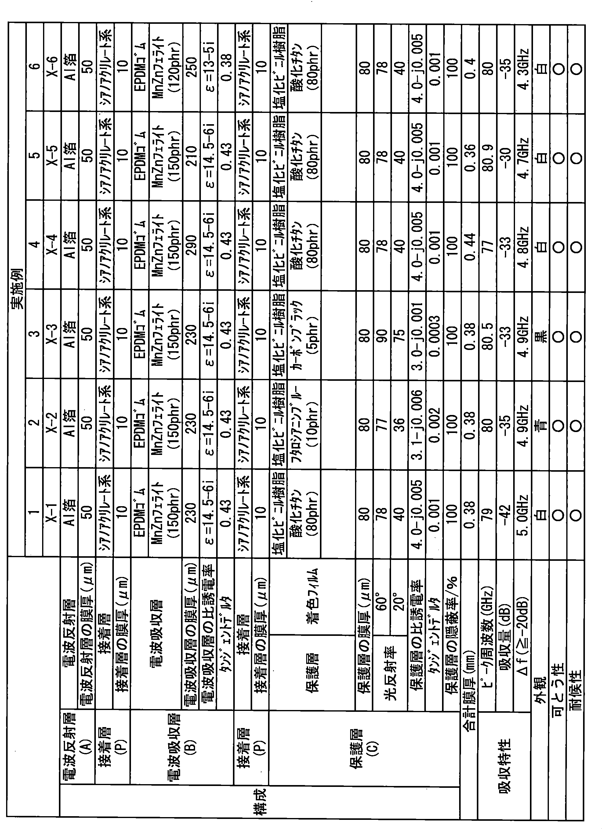

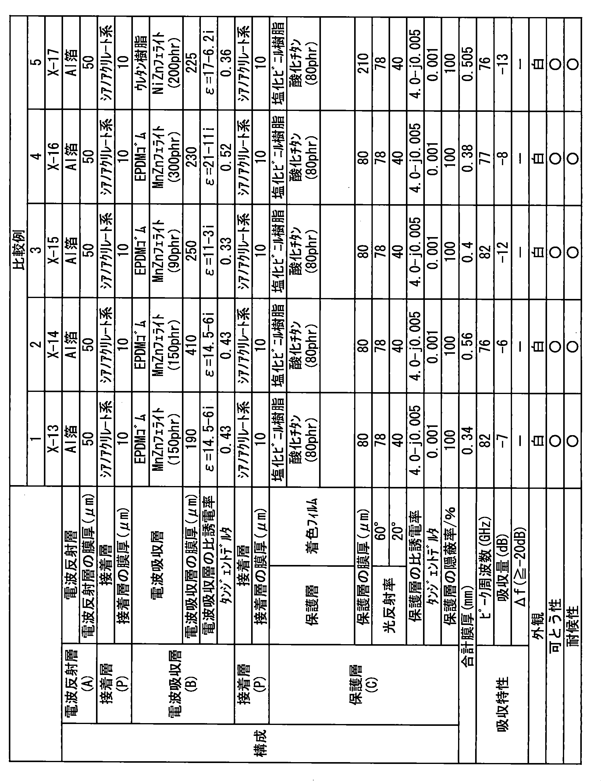

(注)MnZnフェライト:マンガン・亜鉛系フェライト、平均粒子径0.7μm、
(注)MnNiフェライト:マンガン・ニッケル系フェライト、平均粒子径0.4μm。 (Note) MnZn ferrite: Manganese-zinc ferrite, average particle size 0.7 μm,
(Note) MnNi ferrite: Manganese-nickel ferrite, average particle size 0.4 μm.
(注)MnNiフェライト:マンガン・ニッケル系フェライト、平均粒子径0.4μm。 (Note) MnZn ferrite: Manganese-zinc ferrite, average particle size 0.7 μm,
(Note) MnNi ferrite: Manganese-nickel ferrite, average particle size 0.4 μm.
<評価試験>
上記実施例及び比較例で作成した電波吸収シート(X-1)~(X-22)を下記基準、方法にて評価し、各電波吸収シートが有する性状値と共に表1に示した。尚、表1中、電波吸収層(B)の比誘電率、保護層(C)の入射角度60°の光反射率、及び入射角度20°の光反射率は、明細書記載の方法によって求めたものである。 <Evaluation test>
The radio wave absorbing sheets (X-1) to (X-22) prepared in the above Examples and Comparative Examples were evaluated according to the following criteria and methods, and are shown in Table 1 together with the property values possessed by each radio wave absorbing sheet. In Table 1, the relative dielectric constant of the radio wave absorption layer (B), the light reflectivity at an incident angle of 60 ° of the protective layer (C), and the light reflectivity at an incident angle of 20 ° are determined by the method described in the specification. It is
(*)各電波吸収シートの電波吸収性測定
各電波吸収シートの電波吸収性を、電波吸収量が-30dB以上の電波吸収体を部屋の壁面及び床面に設置した電波暗室にて、ミリ波電波吸収測定装置を用いて測定した。具体的には、電波吸収測定装置に備えられた送信用ホーンアンテナと受信用ホーンアンテナの入射及び反射角度が、床面からの垂直面に対し、それぞれ10°となるように、送信用ホーンアンテナと受信用ホーンアンテナを設置し、それぞれのアンテナから45cmの距離となるように金属反射板を置き、反射してくる信号を受信用ホーンアンテナで受信して、その電波反射率を100%とする。次に金属反射板を取除き反射してくる信号を受信用ホーンアンテナで受信してその電波反射率を0%とする。そして金属反射板を置いた位置に測定試料を置き、種々の周波数について測定試料表面から反射してくる電波反射量を測定し、周波数(GHz)を横軸とし、電波吸収量(dB)を縦軸とする電波吸収特性チャートを得た。図2に電波吸収特性チャートの一例を示す。 (*) Measurement of wave absorption of each wave absorption sheet The wave absorption of each wave absorption sheet is measured by using a wave anechoic chamber with a wave absorption of -30 dB or more on a wall and floor of a room. It measured using the electromagnetic wave absorption measuring apparatus. Specifically, the transmitting horn antenna is arranged such that the incident and reflection angles of the transmitting horn antenna and the receiving horn antenna provided in the radio wave absorption measuring apparatus are each 10 ° with respect to the vertical plane from the floor surface. Install a receiving horn antenna, place a metal reflector so that the distance from each antenna is 45 cm, receive the reflected signal with the receiving horn antenna, and set the radio wave reflectivity to 100%. . Next, the metal reflector is removed and the signal reflected is received by the receiving horn antenna, and the radio wave reflectance is made 0%. Then, place the measurement sample at the position where the metal reflector is placed, measure the amount of reflection of radio waves reflected from the surface of the measurement sample at various frequencies, set the frequency (GHz) as the horizontal axis, and measure the amount of radio absorption (dB) vertically. The axis of radio wave absorption characteristic chart was obtained. FIG. 2 shows an example of the radio wave absorption characteristic chart.
各電波吸収シートの電波吸収性を、電波吸収量が-30dB以上の電波吸収体を部屋の壁面及び床面に設置した電波暗室にて、ミリ波電波吸収測定装置を用いて測定した。具体的には、電波吸収測定装置に備えられた送信用ホーンアンテナと受信用ホーンアンテナの入射及び反射角度が、床面からの垂直面に対し、それぞれ10°となるように、送信用ホーンアンテナと受信用ホーンアンテナを設置し、それぞれのアンテナから45cmの距離となるように金属反射板を置き、反射してくる信号を受信用ホーンアンテナで受信して、その電波反射率を100%とする。次に金属反射板を取除き反射してくる信号を受信用ホーンアンテナで受信してその電波反射率を0%とする。そして金属反射板を置いた位置に測定試料を置き、種々の周波数について測定試料表面から反射してくる電波反射量を測定し、周波数(GHz)を横軸とし、電波吸収量(dB)を縦軸とする電波吸収特性チャートを得た。図2に電波吸収特性チャートの一例を示す。 (*) Measurement of wave absorption of each wave absorption sheet The wave absorption of each wave absorption sheet is measured by using a wave anechoic chamber with a wave absorption of -30 dB or more on a wall and floor of a room. It measured using the electromagnetic wave absorption measuring apparatus. Specifically, the transmitting horn antenna is arranged such that the incident and reflection angles of the transmitting horn antenna and the receiving horn antenna provided in the radio wave absorption measuring apparatus are each 10 ° with respect to the vertical plane from the floor surface. Install a receiving horn antenna, place a metal reflector so that the distance from each antenna is 45 cm, receive the reflected signal with the receiving horn antenna, and set the radio wave reflectivity to 100%. . Next, the metal reflector is removed and the signal reflected is received by the receiving horn antenna, and the radio wave reflectance is made 0%. Then, place the measurement sample at the position where the metal reflector is placed, measure the amount of reflection of radio waves reflected from the surface of the measurement sample at various frequencies, set the frequency (GHz) as the horizontal axis, and measure the amount of radio absorption (dB) vertically. The axis of radio wave absorption characteristic chart was obtained. FIG. 2 shows an example of the radio wave absorption characteristic chart.
(*)ピーク周波数における電波吸収量
上記電波吸収量測定で得られた電波吸収特性チャートにおいて、最も電波吸収量が多い周波数をピーク周波数とし、該ピーク周波数における電波吸収量を求め、表中に記載した。尚、表中の電波吸収量は数値が低いほど、電波吸収量が多く、良好であることを意味する。 (*) Radio wave absorption amount at peak frequency In the radio wave absorption characteristic chart obtained by the above radio wave absorption amount measurement, the frequency with the largest radio wave absorption amount is taken as the peak frequency, radio wave absorption amount at the peak frequency is determined, did. The lower the value of the radio wave absorption in the table, the larger the radio wave absorption, which means that the better.
上記電波吸収量測定で得られた電波吸収特性チャートにおいて、最も電波吸収量が多い周波数をピーク周波数とし、該ピーク周波数における電波吸収量を求め、表中に記載した。尚、表中の電波吸収量は数値が低いほど、電波吸収量が多く、良好であることを意味する。 (*) Radio wave absorption amount at peak frequency In the radio wave absorption characteristic chart obtained by the above radio wave absorption amount measurement, the frequency with the largest radio wave absorption amount is taken as the peak frequency, radio wave absorption amount at the peak frequency is determined, did. The lower the value of the radio wave absorption in the table, the larger the radio wave absorption, which means that the better.
(*)電波吸収量が-20dB以上となる帯域幅
電波吸収量-20dBにおける、最大吸収周波数fuと最小吸収周波数flとの差であり、次式で表される。bw=fu-fl。 (*) Bandwidth at which the radio wave absorption amount is -20 dB or more The difference between the maximum absorption frequency fu and the minimum absorption frequency fl at the radio wave absorption amount of -20 dB, which is expressed by the following equation. bw = fu-fl.
電波吸収量-20dBにおける、最大吸収周波数fuと最小吸収周波数flとの差であり、次式で表される。bw=fu-fl。 (*) Bandwidth at which the radio wave absorption amount is -20 dB or more The difference between the maximum absorption frequency fu and the minimum absorption frequency fl at the radio wave absorption amount of -20 dB, which is expressed by the following equation. bw = fu-fl.
表中の数値が大きいほどミリ波領域での帯域幅が広いことを意味し、良好である。尚、表中「-」の記号は電波吸収量が-20dBに達していないために、幅が測定できないことを意味する。
The larger the numerical values in the table, the wider the bandwidth in the millimeter wave region, and the better. In the table, the symbol "-" means that the width can not be measured because the radio wave absorption amount has not reached -20 dB.
(*)可とう性
各電波吸収シート(X-1)~(X-22)を、電波反射層が下となるように180°手で折り曲げ、折り曲げ作業性と折り曲げ部の表面状態を下記基準にて評価した。
○:折り曲げ作業性は良好であり、折り曲げ部に破損が全く認められない、
△:折り曲げ作業性は良好であるが、折り曲げ部に破損が若干認められる、
×:折り曲げ作業が困難であり、折り曲げ部に著しい破損が認められる。 (*) Flexibility Each radio wave absorption sheet (X-1) to (X-22) is bent by 180 ° so that the radio wave reflection layer is on the bottom, and the bending workability and the surface condition of the bent part are based on the following criteria It evaluated by.
○: The bending workability is good, and no breakage is observed at the bending portion at all.
Δ: Although the bending workability is good, some breakage is observed at the bending portion,
X: The bending operation is difficult, and significant breakage is observed at the bending portion.
(*耐候性)
促進耐候性試験には、JIS B 7754に規定されたスーパーキセノンウェザオメーター(商品名、スガ試験機社製)を使用し、1時間42分間のキセノンアークランプの照射と18分間の降雨の条件による合計2時間を1サイクルとして、500サイクルの繰り返し試験終了後の試験体の目視評価を行なった。
○:シート表面に異常が全く認められず
△:シート表面に初期と比較してわずかにツヤビケが認められるもののワレはなし、
×:シート表面にワレが明らかに認められる。 (*Weatherability)
For the accelerated weathering test, using a super xenon weatherometer (trade name, manufactured by Suga Test Instruments Co., Ltd.) defined in JIS B 7754, conditions of irradiation of a xenon arc lamp for 1 hour and 42 minutes and rainfall for 18 minutes Visual evaluation of the test body after the completion of 500 cycles of repeated tests was performed, with a total of 2 hours by 1 cycle as one cycle.
:: no abnormality was observed on the sheet surface :: slight gloss was observed on the sheet surface compared to the initial level, but no cracking was observed,
X: A crack is clearly recognized on the sheet surface.
(考察)
表1の結果より、本発明の効果について以下に考察する。 (Discussion)
From the results of Table 1, the effects of the present invention are discussed below.
表1の結果より、本発明の効果について以下に考察する。 (Discussion)
From the results of Table 1, the effects of the present invention are discussed below.
実施例1~12は本発明で規定した範囲内の電波吸収シートである。
Examples 1 to 12 are the radio wave absorbing sheets within the range defined in the present invention.
比較例1及び2は電波吸収層(B)の膜厚が本発明で規定した範囲を外れる電波吸収 シートである。
Comparative Examples 1 and 2 are radio wave absorption sheets in which the film thickness of the radio wave absorption layer (B) is out of the range defined in the present invention.
比較例3は電波吸収層(B)に含まれるマンガン・亜鉛フェライトの含有量を減量し、電波吸収層(B)の比誘電率虚数部が本発明で規定する範囲を下回る電波吸収シートである。
Comparative Example 3 is a radio wave absorption sheet in which the content of manganese and zinc ferrite contained in the radio wave absorption layer (B) is reduced and the imaginary part of the relative dielectric constant of the radio wave absorption layer (B) falls below the range specified in the present invention. .
比較例4は電波吸収層(B)に含まれるマンガン・亜鉛フェライトの含有量を増量し、電波吸収層の比誘電率実数部が本発明で規定した範囲を外れる電波吸収シートである。
Comparative Example 4 is a radio wave absorption sheet in which the content of manganese and zinc ferrite contained in the radio wave absorption layer (B) is increased and the real part of the relative permittivity of the radio wave absorption layer deviates from the range defined in the present invention.
比較例5は、保護層(C)の膜厚が本発明で規定した範囲を外れる電波吸収シートである。
Comparative Example 5 is a radio wave absorption sheet in which the thickness of the protective layer (C) is out of the range defined in the present invention.
比較例6は、保護層(C)が備えられていない電波吸収シートである。
The comparative example 6 is a radio wave absorption sheet in which the protective layer (C) is not provided.
比較例7は、電波反射層(A)が備えられていない電波吸収シートである。
The comparative example 7 is a radio wave absorption sheet in which the radio wave reflection layer (A) is not provided.
比較例8及び9は、タンジェントデルタ値が本発明範囲を外れる電波吸収シートである。
The comparative examples 8 and 9 are the electromagnetic wave absorption sheets from which a tangent delta value remove | deviates from the scope of the present invention.
比較例10は、保護層(C)の光反射率が本発明範囲を外れる電波吸収シートである。
Comparative Example 10 is a radio wave absorption sheet in which the light reflectance of the protective layer (C) falls outside the scope of the present invention.
以上により調製された電波吸収シートによるミリ波帯域の電波吸収特性及び可とう性試験、耐候性試験結果より、以下のことが言える。
The following can be said from the radio wave absorption characteristics of the millimeter wave band by the radio wave absorption sheet prepared as described above, the flexibility test, and the weather resistance test results.
電波反射層(A)、電波吸収層(B)及び保護層(C)をすべて備えるとともに配置関係が規定どおりであり、電波吸収層(B)と保護層(C)の膜厚が所定範囲内であり、電波吸収層の比誘電率及び保護層の光反射率が本発明所定の範囲内にある限り、ミリ波吸収性に極めて優れ、帯域幅が広く、可とう性、耐候性に優れた電波吸収シートが得られる。
The radio wave reflection layer (A), the radio wave absorption layer (B) and the protective layer (C) are all provided and the arrangement relationship is as specified, and the film thickness of the radio wave absorption layer (B) and the protective layer (C) is within a predetermined range As long as the relative dielectric constant of the radio wave absorption layer and the light reflectance of the protective layer are within the predetermined range of the present invention, the millimeter wave absorption is extremely excellent, the bandwidth is wide, and the flexibility and the weather resistance are excellent. A radio wave absorbing sheet is obtained.
電波吸収層(B)が膜厚の条件を満たさない場合は、電波吸収シートのミリ波吸収性が充分発揮できないが、電波吸収層(B)膜厚が本発明規定の範囲にあるときに限り、ミリ波電波吸収性と帯域幅が飛躍的に増大する。(実施例1と、比較例1、2との対比)。
When the radio wave absorption layer (B) does not satisfy the film thickness condition, the millimeter wave absorption of the radio wave absorption sheet can not be exhibited sufficiently, but only when the film thickness of the radio wave absorption layer (B) is within the range defined by the present invention. , Millimeter wave wave absorption and bandwidth dramatically increase. (Comparison between Example 1 and Comparative Examples 1 and 2).
電波吸収層(B)が比誘電率の条件を満たさない場合は、電波吸収シートのミリ波吸収性が充分発揮できないが、電波吸収層(B)の比誘電率が本発明規定の範囲にあるときに限り、ミリ波電波吸収性と帯域幅が飛躍的に増大する。(実施例1と、比較例3と4との対比)。
When the radio wave absorption layer (B) does not satisfy the condition of the relative dielectric constant, the millimeter wave absorbability of the radio wave absorption sheet can not be exhibited sufficiently, but the relative dielectric constant of the radio wave absorption layer (B) is within the range defined by the present invention. Only at times, millimeter wave absorption and bandwidth dramatically increase. (Comparison between Example 1 and Comparative Examples 3 and 4).
電波反射層(A)がない電波吸収シートでは、電波吸収シートのミリ波吸収性が充分発揮できない。しかしながら、すべての層を組み合わせることによって、ミリ波電波吸収性と帯域幅が飛躍的に増大する。(実施例1と7との対比)。
In the radio wave absorption sheet without the radio wave reflection layer (A), the millimeter wave absorption of the radio wave absorption sheet can not be sufficiently exhibited. However, the combination of all layers dramatically increases millimeter wave absorption and bandwidth. (Comparison with Examples 1 and 7).
保護層(C)がない電波吸収シートでは、ある程度のミリ波吸収性を有するが十分ではない。また、保護層(C)の膜厚を大きくしすぎた場合も、ミリ波吸収性は十分ではない。(実施例1と比較例5、6との対比)。
In the radio wave absorption sheet without the protective layer (C), although it has a certain degree of millimeter wave absorption, it is not sufficient. Also, when the film thickness of the protective layer (C) is too large, the millimeter wave absorption is not sufficient. (Comparison between Example 1 and Comparative Examples 5 and 6).
電波吸収層(B)のタンジェントデルタ値が規定範囲内にない電波吸収シートでは、ある程度のミリ波吸収性を有するが、全く不十分である。タンジェントデルタ値が本発明規定の範囲にあるときに限り、ミリ波電波吸収性と帯域幅が飛躍的に増大する。(実施例1と比較例8と9との対比)。
The radio wave absorption sheet in which the tangent delta value of the radio wave absorption layer (B) is not within the specified range has a certain degree of millimeter wave absorption, but it is not sufficient at all. Only when the tangent delta value falls within the range defined by the present invention, millimeter wave absorption and bandwidth dramatically increase. (Comparison of Example 1 with Comparative Examples 8 and 9).
保護層(C)の光反射率が規定範囲内にない電波吸収シートでは、ある程度のミリ波吸収性を有するが十分ではなく、また耐候性が悪く、実用レベルにはない。(実施例1と比較例10との対比)。
In the radio wave absorption sheet in which the light reflectance of the protective layer (C) is not within the specified range, although it has a certain degree of millimeter wave absorption, it is not sufficient and the weather resistance is poor and it is not in practical use. (Comparison between Example 1 and Comparative Example 10).
Claims (10)
- 電波反射層(A)と、前記電波反射層(A)の上部に平行に配置された電波吸収層(B)と、前記電波吸収層(B)の上部に平行に配置された保護層(C)とを備えてなる、ミリ波帯域用電波吸収シートであって、
前記電波吸収層(B)の周波数79GHzにおける比誘電率の実数部が10~20の範囲内であり、虚数部の絶対値が4~10の範囲内であり、前記電波吸収層(B)の膜厚が200~400μmの範囲内にあり、前記比誘電率の虚数部/実数部の絶対値が0.30~0.60の範囲内にあり、
前記保護層(C)の周波数79GHzにおける比誘電率の実数部が1.5~8.0の範囲内であり、虚数部の絶対値が1.0未満であり、前記保護層(C)の膜厚が50~200μmの範囲内にあり、前記保護層(C)の光反射率が入射角60°で50%以上、入射角20°で25%以上である、ミリ波帯域用電波吸収シート。 A radio wave reflection layer (A), a radio wave absorption layer (B) disposed parallel to the top of the radio wave reflection layer (A), and a protective layer (C) disposed parallel to the top of the radio wave absorption layer (B) A millimeter wave band electromagnetic wave absorbing sheet, comprising
The real part of the relative permittivity at a frequency of 79 GHz of the radio wave absorption layer (B) is in the range of 10 to 20, the absolute value of the imaginary part is in the range of 4 to 10, and the radio wave absorption layer (B) The film thickness is in the range of 200 to 400 μm, and the absolute value of the imaginary part / real part of the relative dielectric constant is in the range of 0.30 to 0.60,
The real part of the relative permittivity at a frequency of 79 GHz of the protective layer (C) is in the range of 1.5 to 8.0, the absolute value of the imaginary part is less than 1.0, and the protective layer (C) Radio wave absorption sheet for millimeter wave band, film thickness is in the range of 50 to 200 μm, light reflectivity of the protective layer (C) is 50% or more at incident angle 60 °, and 25% or more at incident angle 20 ° . - 前記電波吸収層(B)が、誘電性粉末及び結合剤を含むフィルムである、請求項1に記載の電波吸収シート。 The radio wave absorption sheet according to claim 1, wherein the radio wave absorption layer (B) is a film containing a dielectric powder and a binder.
- 前記電波吸収層(B)が、前記電波吸収層(B)に含まれる前記結合剤100質量部を基準として、前記誘電性粉末を50~500質量部含む、請求項2に記載の電波吸収シート。 The radio wave absorption sheet according to claim 2, wherein the radio wave absorption layer (B) contains 50 to 500 parts by mass of the dielectric powder based on 100 parts by mass of the binder contained in the radio wave absorption layer (B). .
- 前記電波吸収層(B)が、前記誘電性粉末を前記結合剤中に分散させた分散物を、膜状に成型したフィルムである、請求項2又は3に記載の電波吸収シート。 The electromagnetic wave absorption sheet according to claim 2 or 3, wherein the electromagnetic wave absorption layer (B) is a film formed by molding a dispersion in which the dielectric powder is dispersed in the binder into a film shape.
- 前記電波吸収層(B)が、前記結合剤、前記誘電性粉末及び溶媒を含む電波吸収塗料組成物を塗布し、乾燥させて形成された塗膜である、請求項2又は3に記載の電波吸収シート。 The radio wave according to claim 2 or 3, wherein the radio wave absorption layer (B) is a coating film formed by applying a radio wave absorption coating composition containing the binder, the dielectric powder and a solvent and drying the composition. Absorbent sheet.
- 前記保護層(C)が、結合剤として塩化ビニル樹脂、ポリウレタン樹脂及びポリオレフィン樹脂から選ばれる少なくとも1種の樹脂を含むフィルムである、請求項1ないし5のいずれか1項に記載の電波吸収シート。 The radio wave absorption sheet according to any one of claims 1 to 5, wherein the protective layer (C) is a film containing at least one resin selected from vinyl chloride resin, polyurethane resin and polyolefin resin as a binder. .
- 前記保護層(C)が、着色剤を含む着色フィルムである、請求項1ないし6のいずれか1項に記載の電波吸収シート。 The radio wave absorption sheet according to any one of claims 1 to 6, wherein the protective layer (C) is a colored film containing a colorant.
- 前記電波反射層(A)、前記電波吸収層(B)及び前記保護層(C)が、この順に平行に配置されてなる、請求項1ないし7のいずれか1項に記載の電波吸収シート。 The radio wave absorption sheet according to any one of claims 1 to 7, wherein the radio wave reflection layer (A), the radio wave absorption layer (B), and the protective layer (C) are disposed in parallel in this order.
- 請求項1ないし8のいずれか1項に記載の電波吸収シートを用いる、ミリ波帯域の電波吸収方法。 A millimeter wave band radio wave absorbing method using the radio wave absorbing sheet according to any one of claims 1 to 8.
- 誤作動の電波障害を生じる原因となる電波反射体に、請求項1~8のいずれか1項に記載の電波吸収シートを設置するか、又は、前記電波反射体と電波受信装置との間に、請求項1~8のいずれか1項に記載の電波吸収シートを設置する、電波障害の防止方法。 A radio wave absorbing sheet according to any one of claims 1 to 8 is installed on a radio wave reflector which causes radio wave interference of malfunction, or between the radio wave reflector and the radio wave receiver. A method for preventing radio wave interference, comprising installing the radio wave absorption sheet according to any one of claims 1 to 8.
Priority Applications (4)
| Application Number | Priority Date | Filing Date | Title |
|---|---|---|---|
| US16/756,925 US11509061B2 (en) | 2017-10-19 | 2018-06-27 | Milliwave band radio wave absorption sheet and milliwave radio wave absorption method |
| JP2018555694A JP6524356B1 (en) | 2017-10-19 | 2018-06-27 | Radio wave absorption sheet for millimeter wave band and millimeter wave radio wave absorption method |
| EP18868717.2A EP3700317B1 (en) | 2017-10-19 | 2018-06-27 | Milliwave band radio wave absorption sheet and milliwave radio wave absorption method |
| CN201880067736.7A CN111226511B (en) | 2017-10-19 | 2018-06-27 | Electromagnetic wave absorbing sheet for millimeter wave band, electromagnetic wave absorbing method, and electromagnetic wave failure preventing method |
Applications Claiming Priority (2)
| Application Number | Priority Date | Filing Date | Title |
|---|---|---|---|
| JP2017202368 | 2017-10-19 | ||
| JP2017-202368 | 2017-10-19 |
Publications (1)
| Publication Number | Publication Date |
|---|---|
| WO2019077808A1 true WO2019077808A1 (en) | 2019-04-25 |
Family
ID=66173960
Family Applications (1)
| Application Number | Title | Priority Date | Filing Date |
|---|---|---|---|
| PCT/JP2018/024462 WO2019077808A1 (en) | 2017-10-19 | 2018-06-27 | Milliwave band radio wave absorption sheet and milliwave radio wave absorption method |
Country Status (5)
| Country | Link |
|---|---|
| US (1) | US11509061B2 (en) |
| EP (1) | EP3700317B1 (en) |
| JP (1) | JP6524356B1 (en) |
| CN (1) | CN111226511B (en) |
| WO (1) | WO2019077808A1 (en) |
Cited By (1)
| Publication number | Priority date | Publication date | Assignee | Title |
|---|---|---|---|---|
| KR20220073553A (en) * | 2020-11-26 | 2022-06-03 | 한국교통대학교산학협력단 | Electromagnetic wave shielding sheet and electronic device comprising the same |
Families Citing this family (2)
| Publication number | Priority date | Publication date | Assignee | Title |
|---|---|---|---|---|
| WO2020230708A1 (en) * | 2019-05-14 | 2020-11-19 | 富士フイルム株式会社 | Radio wave absorber |
| US20230042017A1 (en) * | 2019-12-27 | 2023-02-09 | Maxell, Ltd. | Measurement system and radio wave blocking unit |
Citations (7)
| Publication number | Priority date | Publication date | Assignee | Title |
|---|---|---|---|---|
| JPH06334382A (en) | 1993-03-23 | 1994-12-02 | Mitsubishi Heavy Ind Ltd | Wave absorber |
| JPH08288684A (en) | 1995-04-20 | 1996-11-01 | K Lab:Kk | Electromagnetic wave absorber |
| JP2000261180A (en) * | 1999-03-05 | 2000-09-22 | Murata Mfg Co Ltd | Radio wave absorber |
| JP2001217645A (en) | 2000-02-04 | 2001-08-10 | Tdk Corp | Radio wave absorption panel for automatic toll collection system and suppressing method against unwanted radio waves |
| JP2002271084A (en) * | 2001-03-09 | 2002-09-20 | Yokohama Rubber Co Ltd:The | Manufacturing method and program for electromagnetic wave absorber |
| JP2002353682A (en) * | 2001-05-25 | 2002-12-06 | Mitsubishi Cable Ind Ltd | Wave absorber |
| JP2003133784A (en) * | 2001-10-26 | 2003-05-09 | Nitto Denko Corp | Electromagnetic absorber and material thereof |
Family Cites Families (18)
| Publication number | Priority date | Publication date | Assignee | Title |
|---|---|---|---|---|
| JPS62183599A (en) * | 1986-02-07 | 1987-08-11 | 防衛庁技術研究本部長 | Electromagnetic wave absorber |
| JPH0783195B2 (en) * | 1986-12-19 | 1995-09-06 | 東レ株式会社 | Matched electromagnetic wave absorber |
| JP2000031686A (en) * | 1998-07-09 | 2000-01-28 | Daido Steel Co Ltd | Laminated electromagnetic wave absorber and production thereof |
| JP2001168575A (en) * | 1999-12-08 | 2001-06-22 | Sony Corp | Radio wave absorber and method of its manufacture |
| JP2003198179A (en) | 2001-12-26 | 2003-07-11 | Nitto Denko Corp | Electromagnetic wave absorber |
| KR101067731B1 (en) * | 2004-12-03 | 2011-09-28 | 니타 가부시키가이샤 | Electromagnetic interference inhibitor, antenna device and electronic communication apparatus |
| JP2009021403A (en) * | 2007-07-12 | 2009-01-29 | Alps Electric Co Ltd | Electromagnetic wave suppressing sheet |
| JP2010080911A (en) * | 2008-04-30 | 2010-04-08 | Tayca Corp | Wide band electromagnetic wave absorbing material and method of manufacturing same |
| JP2011233834A (en) * | 2010-04-30 | 2011-11-17 | Shachihata Inc | Electromagnetic wave absorber |
| JP5831921B2 (en) * | 2011-03-30 | 2015-12-09 | 日東電工株式会社 | Electromagnetic wave absorber and method for producing electromagnetic wave absorber |
| GB201117480D0 (en) * | 2011-10-10 | 2011-11-23 | Palikaras George | Filter |
| JP6063631B2 (en) * | 2012-03-26 | 2017-01-18 | 日東電工株式会社 | Electromagnetic wave absorber and method for producing electromagnetic wave absorber |
| JP6266242B2 (en) * | 2013-07-16 | 2018-01-24 | 東レ株式会社 | Electromagnetic wave absorber and method for producing the same |
| CN105101769A (en) * | 2015-07-31 | 2015-11-25 | 武汉理工大学 | Embedded composite meta-material absorber |
| US10843445B2 (en) * | 2015-11-25 | 2020-11-24 | Tomoegawa Co., Ltd. | Matched-type electromagnetic wave absorber |
| WO2017111122A1 (en) * | 2015-12-25 | 2017-06-29 | 日本ゼオン株式会社 | Electromagnetic-wave-absorbing material, electromagnetic wave absorber, and method for manufacturing said material and absorber |
| EP3478046A4 (en) * | 2016-06-22 | 2020-02-19 | Maxell Holdings, Ltd. | Electric wave absorption sheet |
| TWI763888B (en) * | 2017-07-20 | 2022-05-11 | 日商麥克賽爾股份有限公司 | Electromagnetic wave absorbing composition, electromagnetic wave absorber |
-
2018
- 2018-06-27 US US16/756,925 patent/US11509061B2/en active Active
- 2018-06-27 WO PCT/JP2018/024462 patent/WO2019077808A1/en unknown
- 2018-06-27 EP EP18868717.2A patent/EP3700317B1/en active Active
- 2018-06-27 JP JP2018555694A patent/JP6524356B1/en active Active
- 2018-06-27 CN CN201880067736.7A patent/CN111226511B/en active Active
Patent Citations (7)
| Publication number | Priority date | Publication date | Assignee | Title |
|---|---|---|---|---|
| JPH06334382A (en) | 1993-03-23 | 1994-12-02 | Mitsubishi Heavy Ind Ltd | Wave absorber |
| JPH08288684A (en) | 1995-04-20 | 1996-11-01 | K Lab:Kk | Electromagnetic wave absorber |
| JP2000261180A (en) * | 1999-03-05 | 2000-09-22 | Murata Mfg Co Ltd | Radio wave absorber |
| JP2001217645A (en) | 2000-02-04 | 2001-08-10 | Tdk Corp | Radio wave absorption panel for automatic toll collection system and suppressing method against unwanted radio waves |
| JP2002271084A (en) * | 2001-03-09 | 2002-09-20 | Yokohama Rubber Co Ltd:The | Manufacturing method and program for electromagnetic wave absorber |
| JP2002353682A (en) * | 2001-05-25 | 2002-12-06 | Mitsubishi Cable Ind Ltd | Wave absorber |
| JP2003133784A (en) * | 2001-10-26 | 2003-05-09 | Nitto Denko Corp | Electromagnetic absorber and material thereof |
Non-Patent Citations (1)
| Title |
|---|
| See also references of EP3700317A4 |
Cited By (2)
| Publication number | Priority date | Publication date | Assignee | Title |
|---|---|---|---|---|
| KR20220073553A (en) * | 2020-11-26 | 2022-06-03 | 한국교통대학교산학협력단 | Electromagnetic wave shielding sheet and electronic device comprising the same |
| KR102495696B1 (en) * | 2020-11-26 | 2023-02-06 | 한국교통대학교산학협력단 | Electromagnetic wave shielding sheet and electronic device comprising the same |
Also Published As
| Publication number | Publication date |
|---|---|
| CN111226511A (en) | 2020-06-02 |
| JPWO2019077808A1 (en) | 2019-11-14 |
| EP3700317B1 (en) | 2022-07-13 |
| JP6524356B1 (en) | 2019-06-05 |
| CN111226511B (en) | 2022-02-11 |
| US11509061B2 (en) | 2022-11-22 |
| US20210194147A1 (en) | 2021-06-24 |
| EP3700317A1 (en) | 2020-08-26 |
| EP3700317A4 (en) | 2021-07-14 |
Similar Documents
| Publication | Publication Date | Title |
|---|---|---|
| JP6524356B1 (en) | Radio wave absorption sheet for millimeter wave band and millimeter wave radio wave absorption method | |
| WO2020111159A1 (en) | Quasi-millimeter wave/millimeter wave band electric wave absorption sheet and quasi-millimeter wave/millimeter wave band electric wave absorption method | |
| CN101636449B (en) | Resin composition | |
| JP6437168B2 (en) | Radio wave absorption sheet for millimeter wave band and millimeter wave radio wave absorption method | |
| JP4073933B2 (en) | Electromagnetic wave absorber | |
| Kondawar et al. | Theory of EMI shielding | |
| WO2006035912A1 (en) | Electromagnetic wave absorber | |
| US20150042502A1 (en) | Electromagnetic radiation attenuator | |
| JP7442457B2 (en) | Radar standing wave attenuation components and systems | |
| JP4528334B2 (en) | Electromagnetic wave absorber | |
| JP4108677B2 (en) | Electromagnetic wave absorber | |
| CN101395485A (en) | Electronic apparatus test device and electronic apparatus test box | |
| Kim et al. | Microwave absorbers of two-layer composites laminate for wide oblique incidence angles | |
| JP3647447B2 (en) | Electromagnetic wave absorber | |
| CN108092006B (en) | Layered broadband radar wave absorbing plate and preparation method thereof | |
| JP2021145033A (en) | Sheet member and millimeter wave absorber including the same | |
| JP2004128171A (en) | Electric wave absorber | |
| JP2005228939A (en) | Electromagnetic wave absorber and its production process | |
| WO2024029575A1 (en) | Radio wave reflecting body, manufacturing method for radio wave reflecting body, construction method for radio wave reflecting body | |
| CN111562551A (en) | Radar scattering cross section enhanced surface structure for vehicle-mounted radar test | |
| Seng et al. | Improved rice husk ash microwave absorber with CNTs | |
| Liubetski et al. | Creation of radar-absorbing structures based on carbon films | |
| RU2644399C1 (en) | Composite radar absorbent material and method of its manufacture | |
| JP2002245499A (en) | Etc system | |
| JPH11330775A (en) | Transparent laminated-type radio wave anti-reflection body and method thereof |
Legal Events
| Date | Code | Title | Description |
|---|---|---|---|
| ENP | Entry into the national phase |
Ref document number: 2018555694 Country of ref document: JP Kind code of ref document: A |
|
| 121 | Ep: the epo has been informed by wipo that ep was designated in this application |
Ref document number: 18868717 Country of ref document: EP Kind code of ref document: A1 |
|
| NENP | Non-entry into the national phase |
Ref country code: DE |
|
| ENP | Entry into the national phase |
Ref document number: 2018868717 Country of ref document: EP Effective date: 20200519 |