WO2019075698A1 - 模组结构、模组加工方法和终端设备 - Google Patents
模组结构、模组加工方法和终端设备 Download PDFInfo
- Publication number
- WO2019075698A1 WO2019075698A1 PCT/CN2017/106910 CN2017106910W WO2019075698A1 WO 2019075698 A1 WO2019075698 A1 WO 2019075698A1 CN 2017106910 W CN2017106910 W CN 2017106910W WO 2019075698 A1 WO2019075698 A1 WO 2019075698A1
- Authority
- WO
- WIPO (PCT)
- Prior art keywords
- circuit board
- module structure
- chip
- module
- pads
- Prior art date
- Legal status (The legal status is an assumption and is not a legal conclusion. Google has not performed a legal analysis and makes no representation as to the accuracy of the status listed.)
- Ceased
Links
Images



Classifications
-
- G—PHYSICS
- G06—COMPUTING OR CALCULATING; COUNTING
- G06F—ELECTRIC DIGITAL DATA PROCESSING
- G06F1/00—Details not covered by groups G06F3/00 - G06F13/00 and G06F21/00
- G06F1/16—Constructional details or arrangements
Definitions
- Embodiments of the present application relate to the field of module processing, and more particularly, to a module structure, a module processing method, and a terminal device.
- fingerprint recognition technology has been widely used in electronic devices such as smart phones, and other fields that require the use of biometrics. Users are increasingly demanding fingerprint recognition modules.
- the traditional fingerprint module structure is due to the production assembly process. Restrictions have been unable to meet the needs of users. Therefore, how to achieve a thinner and smaller module structure is an urgent problem to be solved.
- the embodiment of the present application provides a module structure, a module processing method, and a terminal device, which can reduce the thickness of the module structure.
- a module structure comprising:
- the first surface of the chip is provided with a plurality of first pads
- circuit board having a plurality of second pads disposed on a second surface thereof, the first surface of the chip being coupled to the second surface of the circuit board;
- An electrical connection assembly for electrically connecting the plurality of first pads and the plurality of second pads
- cover plate being coupled to the first surface of the circuit board.
- the module structure of the embodiment of the present application eliminates the reinforcing structure, simplifies the module structure, helps reduce the thickness of the module structure, and sets the circuit board on the chip and Between the cover plates, the circuit board is absorbing external force, thereby improving the mechanical reliability of the module structure.
- the circuit board is a hollowed out structure.
- the hollow structure may be a hollow structure.
- the module structure further includes:
- a physical connection assembly for connecting a first surface of the chip and a second table of the circuit board And a first surface and the cover plate connecting the circuit board.
- the physical connection component is a non-conductive material.
- the physical connection component may adopt at least one of the following adhesive materials: Thermal Compression Non-Conductive Paste (TCNCP), Thermal Compression Non-Conductive Film (Thermal Compression Non-Conductive Film, TCNCF), Die Attach Film (DAF) or Silver (Epoxy).
- TCNCP Thermal Compression Non-Conductive Paste
- TCNCF Thermal Compression Non-Conductive Film
- DAF Die Attach Film
- Silver Silver
- the physical connection component has a dielectric constant greater than three.
- the circuit board is a flexible circuit board FPC.
- the thickness of the FPC is thin, and the FPC type circuit board is used to reduce the thickness of the module structure.
- the FPC type circuit board can improve the assembly flexibility.
- the electrical connection component is a metal bump or a conductive particle.
- Conductive particles are used as a medium for signal transmission between the chip and the circuit board. Therefore, during the processing of the module, the required processing temperature is low, thereby reducing the influence of high temperature on the warpage of the chip, thereby enabling Improve the reliability of the module structure.
- the metal bumps are gold bumps, copper bumps, tin bumps, and the like.
- the conductive particles are a metal powder, a metal ball or a polymer plastic ball coated with a metal surface.
- the cover material is plexiglass, glass, ceramic or sapphire or the like.
- the chip is a fingerprint sensing chip.
- a module processing method including:
- An electrical connection assembly is fabricated between the first surface of the chip and the second surface of the circuit board, the plurality of first pads and the plurality of second pads being electrically connected by the electrical connection assembly.
- the method further includes:
- a physical connection assembly is prepared on the cover.
- the method further includes:
- a physical connection assembly is fabricated on the second surface of the circuit board.
- the method before the first surface of the circuit board is mounted on the cover, the method further includes:
- the partial area on the circuit board is hollowed out.
- the cover plate in the process of module processing, is placed at the bottom of the module structure to function as an existing reinforcing structure, and in actual use, the cover is used.
- the plate is placed at the top of the module structure and functions as an existing cover plate. Therefore, the cover plate according to the embodiment of the present application has the functions of reinforcing structure and cover plate, and the module structure is simplified. Helps reduce the thickness of the module structure.
- a terminal device including:
- a fourth aspect provides a terminal device, including:
- Figure 1 is a schematic diagram of a module structure.
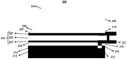
- FIG. 2 is a schematic diagram of a longitudinal section of a module structure in accordance with an embodiment of the present application.
- FIG. 3 is a schematic diagram of a longitudinal section of a module structure in accordance with another embodiment of the present application.
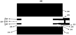
- FIG. 4 is a schematic diagram of a cross-section of a module structure in accordance with another embodiment of the present application.
- FIG. 5 is a schematic flowchart of a module processing method according to an embodiment of the present application.
- FIG. 6 is a schematic structural diagram of a terminal device according to an embodiment of the present application.
- the module structure 100 includes a cover 110, a physical connection component 120, a chip 130, and a circuit board 150 for implementing pads 131 and circuits of the chip 130.
- a connector e.g., solder ball
- solder ball 140 that electrically connects between the pads 151 of the board 150, and a reinforcing structure 160.
- the embodiment of the present application provides a module structure, which can reduce the thickness of the module structure.
- the module structure 200 includes:
- the first surface 212 of the chip is provided with a plurality of first pads 211;
- circuit board 220 the second surface 224 of the circuit board is provided with a plurality of second pads 221, and the first surface 212 of the chip is connected to the second surface 224 of the circuit board;
- the electrical connection component 230 is configured to electrically connect the plurality of first pads 211 and the plurality of second pads 221;
- a cover plate 240 is coupled to the first surface 225 of the circuit board.
- the module structure of the embodiment of the present application is a chip, an electrical connection component, a circuit board and a cover plate in order from the bottom to the top, which can be understood by those skilled in the art, during the processing of the module, or in actual use.
- the embodiment of the present application is described by taking the cover at the top of the module structure as an example, and should not be construed as limiting the embodiment of the present application.
- the cover plate 240 of the embodiment of the present application has the function of the cover plate and the reinforcing structure in the existing module structure.
- the cover plate 240 of the embodiment of the present application may have a cover.
- the function of the board, in the processing of the module structure, the cover 240 of the embodiment of the present application can be placed at the bottom of the module structure, so as to play the role of reinforcing material, the specific implementation process is as follows An embodiment of the module processing method described herein.
- the module structure of the embodiment of the present application eliminates the reinforcing structure, simplifies the module structure, helps reduce the thickness of the module structure, and sets the circuit board on the chip and Between the cover plates, the circuit board is absorbing external force, thereby improving the mechanical reliability of the module structure.
- the upper surface of the structural member may become the lower surface of the structural member, and therefore, the upper surface or the lower surface of each structural member is not absolutely, in relation to the placement state of the structural member, in the embodiment of the present application, the upper surface of each structural member is referred to as the first surface of each structural member when the cover is placed upward, The lower surface of each structural member when the cover is placed upward is referred to as the second surface of each structural member, for example, the first surface 225 of the circuit board is the upper surface of the circuit board when the cover is placed upward, the circuit board The second surface 224 is the lower surface of the circuit board when the cover is placed upward.
- the chip in the embodiment of the present application may be a fingerprint sensing chip, such as an optical fingerprint chip, a capacitive fingerprint chip, or an ultrasonic fingerprint chip, or may be a chip for implementing other functions.
- the fingerprint sensor chip is used as an example, but the present invention should not be limited.
- the module structure of the embodiment of the present application also falls within the protection scope of the embodiment of the present application.
- the plurality of first pads 211 of the chip can be understood as pins that are electrically connected to the other structural components, that is, the chip 210 can be realized by the plurality of first pads 211 and other structural components, for example, a circuit board. 220 electrical connection. It should be understood that, in the embodiment of the present application, the plurality of first pads 210 may be uniformly or unevenly distributed on the first surface 212 of the chip, and the first solder in the module structure 200 shown in FIG. 2 The number and location of the disks 211 are merely examples and are not limiting.
- the plurality of second pads 221 of the circuit board can be understood as the pins that the circuit board 220 is electrically connected to other structural components, that is, the circuit board 220 can be realized with other structural components through the plurality of second pads 221.
- the electrical connection of the chip 210 may be uniformly or unevenly distributed on the second surface 224 of the circuit board, and the second soldering in the module structure 200 shown in FIG.
- the number and location of disks 221 are merely examples and are not limiting.
- the circuit board 220 may be a Flexible Printed Circuit (FPC).
- FPC Flexible Printed Circuit
- the thickness of the FPC is thin, and the FPC type circuit board is used to reduce the thickness of the module structure.
- the FPC type circuit board can be used. Increase the flexibility of assembly.
- other types of circuit boards such as a soft and hard bonding board, may also be used in the embodiment of the present application, which is not limited in this embodiment.
- the circuit board 220 may further include a substrate 222 and a solder resist layer 223.
- the structure and function of the substrate 222 and the solder resist layer 223 are similar to those of the prior art and will not be described in detail herein.
- the electrical connection component 230 can be used to implement electrical connection between the plurality of first pads 211 and the plurality of second pads 221 . That is, the electrical connection assembly can be used to effect the transfer of electrical signals between the chip and the circuit board.
- the plurality of first pads 211 may be part or all of all the pads included in the chip, and similarly, the plurality of second pads 221 may be circuits. Part or all of all the pads included in the board, that is, not necessarily all of the pads of the chip are to be electrically connected to all the pads of the board, which pads of the chip and the board Which pads need to be electrically connected can be determined according to the functions that the module structure needs to implement.
- the plurality of first pads 211 and the plurality of second pads 221 herein may be two sets of pads that require electrical connection to be established.
- the number and location of the electrical connection assemblies 230 shown in FIG. 2 are merely examples and are not limiting, and the number of the electrical connection assemblies 230 may be one, for example, only one first pad needs to follow a second pad.
- the electrical connection may be established, or may be multiple.
- a plurality of first pads may be electrically connected to the plurality of second pads, and the like.
- the electrical connection component 230 may be a metal bump or a conductive particle.
- the metal bumps and the conductive particles can be used to realize the transmission of electrical signals between the chip and the circuit board. It should be understood that those skilled in the art can select other types of electrical connection materials according to actual needs, as long as they can be realized.
- the electrical connection between the pad of the chip and the pad of the circuit board is sufficient.
- the embodiment of the present application does not specifically limit the specific form of the electrical connection component.
- the metal bumps may be gold bumps, copper bumps, or tin bumps.
- the metal bump when the electrical connection component is a metal bump, the metal bump may be a gold bump, a copper bump or a tin bump, and those skilled in the art may select other materials according to actual needs.
- the metal bumps are provided as long as the metal bumps can transmit electrical signals between the chip and the circuit board.
- the electrical connection component When the electrical connection component is a metal bump, on the other hand, the electrical connection component can not only transfer the electrical signal between the chip and the circuit board, but also can fix the chip and the circuit board. The role of the relative movement of the chip and the circuit board is prevented, that is to say, the electrical connection component can not only realize the electrical connection between the chip and the circuit board, but also realize the physical connection between the chip and the circuit board.
- the conductive particles may be a metal powder, a metal ball or a polymer plastic ball coated with a metal surface.
- the conductive particle when the electrical connection component is a conductive particle, the conductive particle may be a metal powder, a metal ball or a polymer plastic ball coated with a metal surface, etc., and those skilled in the art may also select according to actual needs.
- Other types of conductive particles are provided as long as the conductive particles are capable of transmitting electrical signals between the chip and the board.
- the processing temperature required during the processing of the module is low, thereby reducing the influence of high temperature on the warpage of the chip, and further Can improve the reliability of the module structure.
- the first surface 212 of the chip and the second surface 224 of the circuit board may be connected to the first surface 212 of the chip and the second surface of the circuit board.
- 224 is directly or indirectly connected, for example, the first surface 212 of the chip may be connected to the second surface 224 of the circuit board by the electrical connection assembly 230 described above, or the first surface 212 of the chip may pass
- the first surface 212 of the chip may also be coupled to the circuit board by a first connector (eg, a gel or film)
- the second surface 224 is connected. That is, the first connector is used to implement physical connection between the first surface 212 of the chip and the second surface 224 of the circuit board, or the first connector may be used to fix the chip and the Said circuit board.
- connection of the cover plate and the first surface 225 of the circuit board may mean that the cover plate and the first surface 225 of the circuit board are directly or indirectly connected, for example, the first surface of the circuit board.
- 225 may be coupled to the cover plate 240 by a second connector (eg, a glue or a film, etc.), ie, the second connector may be used to implement the physical properties of the first surface 225 of the circuit board and the cover plate 240 Alternatively, the second connector may be used to secure the circuit board and the cover plate 240.
- the upper and lower surfaces of the cover plate are the same, that is, the upper surface can be used as the lower surface, and the lower surface can also be used as the upper surface. Therefore, the first surface 225 and the cover plate of the circuit board are not particularly limited herein. Which surface is connected.
- the module structure 200 may further include:
- the physical connection assembly 250 is configured to connect the first surface 212 of the chip and the second surface 224 of the circuit board, and to connect the first surface 225 of the circuit board and the cover plate 240.
- the physical connection assembly 250 herein may correspond to the first connector and the second connector described above, in particular, the physical connection assembly 250 is for physically connecting the chip and the circuit board, and physically connecting the circuit board And the cover plate, that is, the physical connection component may be located between the chip and the circuit board, and between the circuit board and the cover plate, functioning as a fixing and insulating, that is, the physical connection component may be a chip, a circuit board, and The cover plates are fixed together to reduce the relative movement between the structures, and at the same time to isolate the electrical signal transmission between the two structural members.
- the electrical connection assembly is for transmitting electrical signals, and no electrical signals are transmitted in the physical connection assembly.
- the physical connection component 250 is generally a non-conductive medium, and the non-conductive medium is used to facilitate stable transmission of the sensing signal.
- the physical connection component may adopt the following adhesive material. At least one of: Thermal Compression Non-Conductive Paste (TCNCP), Thermal Compression Non-Conductive Film (TCNCF), Die Attach Film (DAF) or Silver glue (Epoxy) and so on.
- the physical connection component has a dielectric constant greater than 3.
- non-conductive medium having a dielectric constant greater than 3 is advantageous for ensuring stable transmission of the sensing signal in the physical connection component, thereby improving the reliability of fingerprint recognition.
- the physical connection component between the chip and the circuit board may function to insulate and physically fix adjacent electrical connection components.
- the material of the cover plate 240 may be organic glass, glass, ceramic or sapphire.
- the cover plate 240 may be made of other materials than the above materials.
- the material used in the cover plate 240 in the embodiment of the present application is not particularly limited.
- FIG 3 is a schematic diagram of a longitudinal section of a module structure 200 according to another embodiment of the present application.
- the circuit board 220 in the module structure 200 shown in FIG. 3 is a hollow structure, and the hollow structure here may be a hollow structure, that is, the circuit of the embodiment of the present application. Part of the area of the board 220 can be hollowed out before the module is processed.
- the hollow structure may be filled with a colloid (an example of a physical connection component), and the dielectric constant of the colloid is set to a large value, thereby ensuring that the sensing signal is in the colloid.
- a colloid an example of a physical connection component
- Figure 4 is a schematic illustration of a cross-section of a cross-section of the module structure from a circuit board layer. As shown in FIG. 4, the hollow structure of the circuit board can be filled with a colloid (an example of the physical connection assembly 250).
- a colloid an example of the physical connection assembly 250.
- module structure according to the embodiment of the present application is described in detail above with reference to FIG. 2 to FIG. 4 .
- the structures shown in FIG. 2 to FIG. 4 are only a few possible implementations of the embodiments of the present application, and should not be construed as limiting the present application.
- the embodiments of the present application are not limited thereto.
- module processing method shown in the following is only a possible implementation manner for implementing the module structure of the embodiment of the present application, and should not be limited to the present application.
- the processing method prepares the above module structure.
- FIG. 5 shows detailed steps or operations of the module processing method of the embodiment of the present application, but the steps or operations are merely examples, and other operations of the present application or various operations of FIG. 5 may be performed. The deformation. Moreover, the various steps in FIG. 5 may be performed in a different order than that presented in FIG. 5, and it is possible that not all operations in FIG. 5 are to be performed.
- the method 300 includes the following:
- the carrier plate may be glass, ceramic, metal or other material having similar functions.
- the carrier board can be understood as a carrier that plays a supporting role in the processing of the module. It is not a module structure, only used for the processing process, and can be removed after completing the corresponding steps. board.
- the carrier film can be selectively coated with a structural film or a functional film, for example, an adhesive layer, a sacrificial layer, a buffer layer, and a dielectric film. (dielectric layer) and so on.
- the adhesive layer film and the sacrificial layer film may both be an ultraviolet-curable (Ultra-Violet, UV) glue, a light-to-heat conversion (LTHC) film, or have similar functions and are wafer level. Process compatible materials.
- the dielectric layer film may be polyimide (PI), polybenzoxazole (PBO), Benzocyclobutene (BCB), an epoxy resin supplied by Ajinomoto Co., Ltd. AJinomoto Buildup Film (ABF), Solder Resist Film (SR), etc.
- connection of the first surface of the circuit board to the cover plate is achieved.
- the method 300 further includes:
- a physical connection assembly is prepared on the cover.
- the physical connection component may be an adhesive material. If a side of the cover plate and the carrier board is referred to as a first surface, a side of the cover plate connected to the first surface 225 of the circuit board is referred to as a first The two surfaces, then, preparing the physical connection component on the cover plate may specifically include coating an adhesive material on the second surface of the cover plate 240, and further, the circuit board may be A surface 225 is secured to the second surface of the cover.
- the physical connection component may employ at least one of the following adhesive materials: TCNCP, TCNCF, DAF or Epoxy, and the like.
- a first surface of the chip is mounted on the second surface of the circuit board, wherein the first surface of the chip is provided with a plurality of first pads, the circuit board A plurality of second pads are disposed on the second surface.
- connection of the first surface of the chip to the second surface of the circuit board is achieved.
- the method 300 further includes:
- a physical connection assembly is fabricated on the second surface of the circuit board.
- an adhesive material can be applied to the second surface of the circuit board, and further, the first surface 212 of the chip can be secured to the second surface 224 of the circuit board by the adhesive material.
- the method 300 may further include:
- the electrical connection component may be the structure described in the foregoing embodiments, for example, metal bumps or conductive particles or the like.
- the process of preparing the physical connection component on the second surface of the circuit board may be performed after the S304, or may also be performed simultaneously with the S304, for example, if the electrical connection component is a conductive particle, The conductive particles may be prepared together with a physical connection component, and at the same time, electrical connection and physical connection between the chip and the circuit board are realized, or, if the electrical connection component is a metal bump, after the metal bump is prepared, The physical connection component is filled between the chip and the circuit board, and between the gaps of the metal bumps, which is not limited by the embodiment of the present application.
- the cover in the process of module processing, the cover is placed At the bottom of the module structure, it functions as an existing reinforcing structure.
- the cover plate is placed at the top of the module structure to function as an existing cover plate. Therefore, the present application
- the cover plate in the module structure of the embodiment has the functions of reinforcing structure and cover plate, and the module structure is simplified, which is beneficial to reducing the thickness of the module structure.
- module processing method of the embodiment of the present application may also be other alternatives or equivalent modifications of the various operations in the above steps.
- the embodiment of the present application does not limit the operation process or operation mode adopted in each step.
- module processing method enumerated above may be performed by a robot or a numerically controlled machining method, and the device software or process for executing the module processing method may be executed by executing computer program code stored in the memory. Perform the above module processing method.
- FIG. 6 is a schematic structural diagram of a terminal device 400 according to an embodiment of the present application.
- the terminal device may include a module structure 401.
- the structure 401 can be the module structure 200 shown in FIG. 2 to FIG. 4 or the module structure prepared according to the module processing method 300 described in FIG.
- the terminal device 400 may be a mobile phone, a tablet computer, a notebook computer, a desktop computer, an in-vehicle electronic device, or a wearable smart device.
- the size of the sequence numbers of the foregoing processes does not mean the order of execution sequence, and the order of execution of each process should be determined by its function and internal logic, and should not be applied to the embodiment of the present application.
- the implementation process constitutes any limitation.
Landscapes
- Engineering & Computer Science (AREA)
- Theoretical Computer Science (AREA)
- Human Computer Interaction (AREA)
- Physics & Mathematics (AREA)
- General Engineering & Computer Science (AREA)
- General Physics & Mathematics (AREA)
- Combinations Of Printed Boards (AREA)
Abstract
一种模组结构、模组加工方法和终端设备,能够降低模组结构的厚度,该模组结构(200)包括:芯片(210),所述芯片(210)的第一表面(212)上设置有多个第一焊盘(211);电路板(220),所述电路板(220)的第二表面(224)上设置有多个第二焊盘(221),所述芯片(210)的第一表面(212)和所述电路板(220)的第二表面(224)连接;电连接组件(230),用于电连接所述多个第一焊盘(211)和所述多个第二焊盘(221);盖板(240),所述盖板(240)和所述电路板(220)的第一表面(225)连接。
Description
本申请实施例涉及模组加工领域,并且更具体地,涉及一种模组结构、模组加工方法和终端设备。
目前,指纹识别技术已被广泛应用于智能手机等电子设备,以及其他需要使用生物识别技术的领域,用户对指纹识别模组的要求越来越高,传统的指纹模组结构由于生产组装工艺的限制,已经无法满足用户的需求,因此,如何实现模组结构更薄、更小是一项亟需解决的问题。
发明内容
本申请实施例提供了一种模组结构、模组加工方法和终端设备,能够降低模组结构的厚度。
第一方面,提供了一种模组结构,包括:
芯片,所述芯片的第一表面上设置有多个第一焊盘;
电路板,所述电路板的第二表面上设置有多个第二焊盘,所述芯片的第一表面和所述电路板的第二表面连接;
电连接组件,用于电连接所述多个第一焊盘和所述多个第二焊盘;
盖板,所述盖板和所述电路板的第一表面连接。
因此,相对于现有的模组结构,本申请实施例的模组结构省去了补强结构,简化了模组结构,有利于降低模组结构的厚度,并且,将电路板设置于芯片和盖板之间,有利于电路板吸收外力,进而能够提升模组结构的机械可靠性。
结合第一方面,在第一方面的某些可能的实现方式中,所述电路板为镂空结构。
可选的,所述镂空结构可以为中空结构。
结合第一方面,在第一方面的某些可能的实现方式中,所述模组结构还包括:
物理连接组件,用于连接所述芯片的第一表面和所述电路板的第二表
面,以及连接所述电路板的第一表面和所述盖板。
结合第一方面,在第一方面的某些可能的实现方式中,所述物理连接组件为非导电材质。
可选地,所述物理连接组件可以采用如下粘附材料中的至少一种:热压非导电胶(Thermal Compression Non-Conductive Paste,TCNCP)、热压非导电膜(Thermal Compression Non-Conductive Film,TCNCF)、芯片粘接薄膜(Die Attach Film,DAF)或银胶(Epoxy)等。
结合第一方面,在第一方面的某些可能的实现方式中,所述物理连接组件的介电常数大于3。
结合第一方面,在第一方面的某些可能的实现方式中,所述电路板为柔性电路板FPC。
通常,FPC的厚度较薄,采用FPC类型的电路板,有利于降低模组结构的厚度,另外,由于FPC的柔韧度高,因此,采用FPC类型的电路板能够提升装配灵活度。
结合第一方面,在第一方面的某些可能的实现方式中,所述电连接组件为金属凸块或导电粒子。
采用导电粒子作为所述芯片和电路板之间的信号传递的媒介,那么,在模组加工过程中,所需的加工温度较低,因此,有利于降低高温对芯片翘曲的影响,进而能够提升模组结构的可靠性。
结合第一方面,在第一方面的某些可能的实现方式中,所述金属凸块为金凸块、铜凸块或锡凸块等。
结合第一方面,在第一方面的某些可能的实现方式中,所述导电粒子为金属粉末、金属球或表面涂附金属的高分子塑料球等。
结合第一方面,在第一方面的某些可能的实现方式中,所述盖板的材料为有机玻璃、玻璃、陶瓷或蓝宝石等。
结合第一方面,在第一方面的某些可能的实现方式中,所述芯片为指纹传感芯片。
第二方面,提供了一种模组加工方法,包括:
在载板上贴装盖板;
将电路板的第一表面贴装在所述盖板上;
将芯片的第一表面贴装在所述电路板的第二表面上,其中,所述芯片的
第一表面上设置有多个第一焊盘,所述电路板的第二表面上设置有多个第二焊盘;
在所述芯片的第一表面和所述电路板的第二表面之间制备电连接组件,通过所述电连接组件电连接所述多个第一焊盘和所述多个第二焊盘。
结合第二方面,在第二方面的某些可能的实现方式中,所述方法还包括:
在所述盖板上制备物理连接组件。
结合第二方面,在第二方面的某些可能的实现方式中,所述方法还包括:
在所述电路板的第二表面上制备物理连接组件。
结合第二方面,在第二方面的某些可能的实现方式中,在将电路板的第一表面贴装在所述盖板上之前,所述方法还包括:
对所述电路板上的部分区域进行镂空处理。
因此,本申请实施例的模组加工方法,在模组加工的过程中,将盖板置于模组结构的最下方,起到现有的补强结构的作用,在实际使用时,将盖板置于模组结构的最上方,起到现有的盖板的作用,因此,根据本申请实施例的中的盖板兼具补强结构和盖板的作用,精简了模组结构,有利于降低模组结构的厚度。
第三方面,提供了一种终端设备,包括:
如第一方面或第一方面的任一可能的实现方式中的模组结构。
第四方面,提供了一种终端设备,其特征在于,包括:
根据第二方面或第二方面的任一可能的实现方式中的模组加工方法制备的模组结构。
图1是一种模组结构的示意图。
图2是根据本申请一实施例的模组结构的纵切面的示意图。
图3是根据本申请另一实施例的模组结构的纵切面的示意图。
图4是根据本申请另一实施例的模组结构的横切面的示意图。
图5是根据本申请实施例的模组加工方法的示意性流程图。
图6是根据本申请实施例的终端设备的示意性结构图。
下面将结合附图,对本申请实施例中的技术方案进行描述。
图1是一种模组结构的示意图,如图1所示,该模组结构100包括盖板110、物理连接组件120、芯片130、电路板150,用于实现芯片130的焊盘131和电路板150的焊盘151之间的电连接的连接件(例如,锡球)140,以及补强结构160。
由于组装工艺的限制,上述结构缺一不可,因此,导致模组结构的厚度无法做到更薄,有鉴于此,本申请实施例提供了一种模组结构,能够降低模组结构的厚度。
以下,结合图2至图4,详细介绍本申请实施例的模组结构。
需要说明的是,为便于理解,在以下示出的实施例中,对于不同实施例中示出的结构中,相同的结构采用相同的附图标记,并且为了简洁,省略对相同结构的详细说明。
应理解,以下示出的本申请实施例的模组结构中的各种结构件的高度或厚度,以及模组结构的整体厚度等仅为示例性说明,而不应对本申请构成任何限定。
图2是根据本申请一实施例的模组结构200的纵切面的示意图。如图2所示,该模组结构200包括:
芯片210,所述芯片的第一表面212上设置有多个第一焊盘211;
电路板220,所述电路板的第二表面224上设置有多个第二焊盘221,所述芯片的第一表面212和所述电路板的第二表面224连接;
电连接组件230,用于电连接所述多个第一焊盘211和所述多个第二焊盘221;
盖板240,所述盖板和所述电路板的第一表面225连接。
也就是说,本申请实施例的模组结构从下往上依次为芯片、电连接组件、电路板和盖板,本领域技术人员可以理解,在模组加工过程中,或者,在实际使用中,可能存在模组倒置的情况,为便于理解,本申请实施例以盖板处于模组结构的最上方为例来描述,而不应对本申请实施例构成任何限定。
需要说明的是,本申请实施例的盖板240兼具现有模组结构中的盖板和补强结构的作用,具体的,在实际使用中,本申请实施例的盖板240可以具有盖板的功能,在模组结构的加工过程中,可以将本申请实施例的盖板240置于模组结构的最下方,使其起到补强材料的作用,具体的执行过程参见下
文描述的模组加工方法的实施例。
因此,相对于现有的模组结构,本申请实施例的模组结构省去了补强结构,简化了模组结构,有利于降低模组结构的厚度,并且,将电路板设置于芯片和盖板之间,有利于电路板吸收外力,进而能够提升模组结构的机械可靠性。
应理解,在模组结构的加工过程中,可能存在模组倒置的情况,此时,结构件的上表面可能成为该结构件的下表面,因此,每个结构件的上表面或下表面并非绝对的,跟该结构件的放置状态有关,为便于区分和理解,在本申请实施例中,将盖板朝上放置时每个结构件的上表面称为每个结构件的第一表面,将盖板朝上放置时每个结构体的下表面称为每个结构件的第二表面,例如,电路板的第一表面225为盖板朝上放置时该电路板的上表面,电路板的第二表面224为盖板朝上放置时该电路板的下表面。
需要说明的是,本申请实施例中的芯片可以为指纹传感芯片,例如,光学指纹芯片、电容式指纹芯片或超声波指纹芯片等,或者也可以为用于实现其他功能的芯片,本申请实施例以指纹传感芯片为例进行介绍,但不应对本申请构成任何限定,其他芯片若采用本申请实施例的模组结构同样落入本申请实施例的保护范围内。
所述芯片的多个第一焊盘211可以理解为芯片210与其他结构件电连接的管脚,即芯片210可以通过所述多个第一焊盘211实现与其他结构件,例如,电路板220的电连接。应理解,在本申请实施例中,所述多个第一焊盘210可以均匀地或者不均匀地分布在芯片的第一表面212上,图2所示的模组结构200中的第一焊盘211的数量和位置仅为示例而非限定。
类似地,所述电路板的多个第二焊盘221可以理解为电路板220与其他结构件电连接的管脚,即电路板220可以通过多个第二焊盘221实现与其他结构件,例如,芯片210的电连接。应理解,在本申请实施例中,所述多个第二焊盘221可以均匀地或者不均匀地分布在电路板的第二表面224,图2所示的模组结构200中的第二焊盘221的数量和位置仅为示例而非限定。
可选地,在本申请实施例中,所述电路板220可以为柔性电路板(Flexible Printed Circuit,FPC)。
通常,FPC的厚度较薄,采用FPC类型的电路板,有利于降低模组结构的厚度,另外,由于FPC的柔韧度高,因此,采用FPC类型的电路板能
够提升装配灵活度。可选地,本申请实施例也可以采用软硬结合板等其他类型的电路板,本申请实施例对此不作特别限定。
可选地,在本申请实施例中,如图2所示,所述电路板220还可以包括基材222和阻焊层223。
其中,基材222和阻焊层223的结构和作用跟现有技术类似,这里不做详细介绍。
在本申请实施例中,所述电连接组件230可以用于实现所述多个第一焊盘211和所述多个第二焊盘221之间的电连接。即所述电连接组件可以用于实现芯片和电路板之间的电信号的传递。
应理解,在本申请实施例中,所述多个第一焊盘211可以为所述芯片包括的全部焊盘中的部分或全部,同样地,所述多个第二焊盘221可以为电路板包括的全部焊盘中的部分或全部,即并不一定是所述芯片的全部焊盘都要与所述电路板的全部焊盘建立电连接,所述芯片的哪些焊盘与电路板的哪些焊盘需要建立电连接可以根据该模组结构需要实现的功能决定。这里的多个第一焊盘211和多个第二焊盘221可以为需要建立电连接的两组焊盘。
应理解,图2所示的电连接组件230的数量和位置仅为示例而非限定,所述电连接组件230的数量可以为一个,例如,只有一个第一焊盘需要跟一个第二焊盘建立电连接,或者也可以为多个,例如,有多个第一焊盘需要跟多个第二焊盘建立电连接等,本申请实施例对此不作限定。
可选地,在本申请实施例中,所述电连接组件230可以为金属凸块或导电粒子。
其中,所述金属凸块和导电粒子可以用于实现芯片和电路板之间的电信号的传递,应理解,本领域技术人员也可以根据实际需要,选择其他类型的电连接材料,只要能够实现所述芯片的焊盘和电路板的焊盘之间的电连接即可,本申请实施例并不特别限定电连接组件的具体形式。
可选地,在一些具体的实施例中,所述金属凸块可以为金凸块、铜凸块或锡凸块。
也就是说,当所述电连接组件为金属凸块时,所述金属凸块具体可以为金凸块、铜凸块或锡凸块,本领域技术人员也可以根据实际需要,选择其他材质的金属凸块,只要该金属凸块能够实现电信号在芯片和电路板之间的传递即可。
当所述电连接组件为金属凸块时,从另一方面来讲,所述电连接组件除了可以实现芯片和电路板之间的电信号的传递,还可以起到固定所述芯片和电路板,防止所述芯片和电路板的相对移动的作用,也就是说,所述电连接组件不仅能够实现芯片和电路板之间的电连接,还能实现芯片和电路板之间的物理连接。
可选地,在一些具体的实施例中,所述导电粒子可以为金属粉末、金属球或表面涂附金属的高分子塑料球。
也就是说,当所述电连接组件为导电粒子时,所述导电粒子具体可以为金属粉末、金属球或表面涂附金属的高分子塑料球等,本领域技术人员也可以根据实际需要,选择其他类型的导电粒子,只要该导电粒子能够实现电信号在芯片和电路板之间的传递即可。
若采用导电粒子作为所述芯片和电路板之间的信号传递的媒介,那么,在模组加工过程中,所需的加工温度较低,因此,有利于降低高温对芯片翘曲的影响,进而能够提升模组结构的可靠性。
需要说明的是,在本申请实施例中,所述芯片的第一表面212和所述电路板的第二表面224连接可以指所述芯片的第一表面212和所述电路板的第二表面224直接连接或间接连接,例如,所述芯片的第一表面212可以通过上述的电连接组件230与所述电路板的第二表面224连接,或者,所述芯片的第一表面212除了可以通过所述电连接组件230与所述电路板的第二表面224连接之外,所述芯片的第一表面212还可以通过第一连接件(例如,胶体或胶膜等)与所述电路板的第二表面224连接。即所述第一连接件用于实现所述芯片的第一表面212与所述电路板的第二表面224的物理连接,或者说,所述第一连接件可以用于固定所述芯片与所述电路板。
类似地,所述盖板和所述电路板的第一表面225连接可以指所述盖板和所述电路板的第一表面225直接连接或间接连接,例如,所述电路板的第一表面225可以通过第二连接件(例如,胶体或胶膜等)与所述盖板240连接,即所述第二连接件可以用于实现电路板的第一表面225与所述盖板240的物理连接,或者说,所述第二连接件可以用于固定所述电路板与所述盖板240。
应注意,通常情况下,盖板的上下表面相同,即上表面可以用作下表面,下表面也可以用作上表面,因此,这里不特别限定所述电路板的第一表面225与盖板的哪个表面连接。
可选地,在本申请实施例中,所述模组结构200还可以包括:
物理连接组件250,用于连接所述芯片的第一表面212和所述电路板的第二表面224,以及连接所述电路板的第一表面225和所述盖板240。
这里的物理连接组件250可以对应于上文描述的第一连接件和第二连接件,具体地,所述物理连接组件250用于物理连接所述芯片和电路板,以及物理连接所述电路板和所述盖板,也就是说,物理连接组件可以位于芯片和电路板,以及电路板和盖板之间,起到固定和绝缘的作用,即所述物理连接组件可以将芯片、电路板和盖板固定在一起,有利于减少结构体之间的相对移动,同时还能起到隔绝两个结构件之间的电信号传递的作用。与所述电连接组件不同的是,所述电连接组件是用于传递电信号的,而所述物理连接组件中不传递电信号。
应理解,在本申请实施例中,所述物理连接组件250通常为不导电介质,采用不导电介质有利于实现感应信号的稳定传递,可选地,所述物理连接组件可以采用如下粘附材料中的至少一种:热压非导电胶(Thermal Compression Non-Conductive Paste,TCNCP)、热压非导电膜(Thermal Compression Non-Conductive Film,TCNCF)、芯片粘接薄膜(Die Attach Film,DAF)或银胶(Epoxy)等。
可选地,在本申请实施例中,所述物理连接组件的介电常数大于3。
采用介电常数大于3的不导电介质有利于保证感应信号在所述物理连接组件中的稳定传递,进而能够提升指纹识别的可靠性。
可选地,若所述电连接组件的数量为多个,那么所述芯片和电路板之间的物理连接组件可以起到将相邻的电连接组件之间绝缘隔开及物理固定的作用。
可选地,在本申请实施例中,所述盖板240的材料可以为有机玻璃、玻璃、陶瓷或蓝宝石。
可选地,所述盖板240可以采用除上述材料以外的其他材料,本申请实施例对于所述盖板240所采用的材料不作特别限定。
图3是根据本申请另一实施例的模组结构200的纵切面的示意图,
与图2所示的模组结构不同的是,图3所示的模组结构200中的电路板220为镂空结构,这里的镂空结构可以为中空结构,也就是说,本申请实施例的电路板220中的部分区域可以先进行镂空处理,然后再进行模组加工。
可选地,在本申请实施例中,可以在所述镂空结构中填充胶体(物理连接组件中的一例),通过设置胶体的介电常数为较大的值,从而能够保证感应信号在胶体中的稳定传递。
图4所示为从电路板层横切所述模组结构得到的横切面的示意图,。如图4所示,电路板的中空结构中可以填充胶体(物理连接组件250的一例)。
需要说明的是,上文中结合图2至图4详细说明了根据本申请实施例的模组结构。但图2至图4示出的结构仅为本申请实施例的几种可能的实现方式,而不应对本申请构成任何限定,本申请实施例也不应限于此。
以下,结合图5介绍说明本申请实施例的模组加工方法。
应理解,以下所示出的模组加工方法仅为用于实现本申请实施例的模组结构的可能的实现方式,而不应对本申请构成任何限定,本申请实施例也可以采用其他模组加工方法制备上述模组结构。
还应理解,图5示出了本申请实施例的模组加工方法的详细的步骤或操作,但这些步骤或操作仅是示例,本申请实施例还可以执行其它操作或者图5的各种操作的变形。此外,图5中的各个步骤可以分别按照与图5所呈现的不同的顺序来执行,并且有可能并非要执行图5中的全部操作。
如图5所示,该方法300包括以下内容:
S301:在载板(carrier)上贴装盖板;
其中,载板可以是玻璃、陶瓷、金属或者其他具有相似功能的材料。
本领域技术人员可以理解,载板可以理解为在模组加工过程中起支撑作用的载体,它不属于模组结构,仅用于加工过程,并且,在完成相应的步骤后可以移除该载板。
可选地,载板上可以选择性涂覆结构薄膜或功能性薄膜,例如,粘附层薄膜(adhesive layer)、牺牲层薄膜(sacrificial layer)、缓冲层薄膜(buffer layer)、介电层薄膜(dielectric layer)等。更具体地,粘附层薄膜和牺牲层薄膜均可以是紫外线固化(Ultra-Violet,UV)胶,光热转换(light-to-heat conversion,LTHC)薄膜,或者具有相似功能且与晶圆级工艺兼容的材料。介电层薄膜可以是聚酰亚胺(polyimide,PI)、聚苯并噁唑(PolyBenzoxazole,PBO)、苯并环丁烯(BenzoCycloButene,BCB)、日本味之素公司供应的一种环氧树脂绝缘膜(Ajinomoto Buildup Film,ABF)、抗阻焊剂薄膜(Solder Resist film,SR)等。
S302,将电路板的第一表面贴装到盖板上。
即实现所述电路板的第一表面与盖板的连接。
可选地,所述方法300还包括:
在所述盖板上制备物理连接组件。
可选地,所述物理连接组件可以为粘附材料,若将盖板与载板连接的一面记为第一表面,将盖板与所述电路板的第一表面225连接的一面记为第二表面,那么,在所述盖板上制备物理连接组件可以具体包括在所述盖板240的第二表面上涂覆粘附材料,进一步地,可以通过所述粘附材料将电路板的第一表面225固定在盖板的第二表面上。
可选地,所述物理连接组件可以采用如下粘附材料中的至少一种:TCNCP、TCNCF、DAF或银胶(Epoxy)等。
进一步地,在S303中,将芯片的第一表面贴装在所述电路板的第二表面上,其中,所述芯片的第一表面上设置有多个第一焊盘,所述电路板的第二表面上设置有多个第二焊盘。
即实现芯片的第一表面与电路板的第二表面的连接。
可选地,所述方法300还包括:
在所述电路板的第二表面上制备物理连接组件。
跟S312的执行过程类似,可以电路板的第二表面上涂覆粘附材料,进一步地,可以通过所述粘附材料将芯片的第一表面212固定在电路板的第二表面224上。进一步地,所述方法300还可以包括:
S304,在所述芯片的第一表面和电路板的第二表面之间制备电连接组件,通过所述电连接组件电连接所述多个第一焊盘和多个第二焊盘。
可选地,所述电连接组件可以为前述实施例中描述的结构,例如,金属凸块或导电粒子等。
可选地,在所述电路板的第二表面上制备物理连接组件的执行过程可以在所述S304之后,或者也可以与所述S304同时执行,例如,若所述电连接组件为导电粒子,所述导电粒子可以与物理连接组件一起制备,同时实现芯片与电路板的电连接和物理连接,或者,若所述电连接组件为金属凸块,可以在制备所述金属凸块后,再将物理连接组件填充至芯片和电路板之间,以及金属凸块的缝隙之间,本申请实施例对此不作限定。
因此,本申请实施例的模组加工方法,在模组加工的过程中,将盖板置
于模组结构的最下方,起到现有的补强结构的作用,在实际使用时,将盖板置于模组结构的最上方,起到现有的盖板的作用,因此,本申请实施例的模组结构中的盖板兼具补强结构和盖板的作用,精简了模组结构,有利于降低模组结构的厚度。
应理解,本申请实施例的模组加工方法还可以为上述步骤中的各种操作的其他替换或等价变形形式,本申请实施例对于每个步骤采用的操作工艺或操作方式不作限定。
还应理解,上述列举的模组加工方法的各实施例,可以通过机器人或者数控加工方式来执行,用于执行模组加工方法的设备软件或工艺可以通过执行保存在存储器中的计算机程序代码来执行上述模组加工方法。
本申请实施例提供了一种终端设备,图6示出了本申请实施例的终端设备400的示意性结构图,如图6所示,该终端设备可以包括模组结构401,所述模组结构401可以为图2至图4所示的模组结构200,或根据图5所述的模组加工方法300制备的模组结构。
作为示例而非限定,所述终端设备400可以为手机、平板电脑、笔记本电脑、台式机电脑、车载电子设备或穿戴式智能设备等。
应理解,在本申请的各种实施例中,上述各过程的序号的大小并不意味着执行顺序的先后,各过程的执行顺序应以其功能和内在逻辑确定,而不应对本申请实施例的实施过程构成任何限定。
以上所述,仅为本申请的具体实施方式,但本申请的保护范围并不局限于此,任何熟悉本技术领域的技术人员在本申请揭露的技术范围内,可轻易想到变化或替换,都应涵盖在本申请的保护范围之内。因此,本申请的保护范围应以所述权利要求的保护范围为准。
Claims (17)
- 一种模组结构,其特征在于,包括:芯片,所述芯片的第一表面上设置有多个第一焊盘;电路板,所述电路板的第二表面上设置有多个第二焊盘,所述芯片的第一表面和所述电路板的第二表面连接;电连接组件,用于电连接所述多个第一焊盘和所述多个第二焊盘;盖板,所述盖板和所述电路板的第一表面连接。
- 根据权利要求1所述的模组结构,其特征在于,所述电路板为镂空结构。
- 根据权利要求1或2所述的模组结构,其特征在于,所述模组结构还包括:物理连接组件,用于连接所述芯片的第一表面和所述电路板的第二表面,以及连接所述电路板的第一表面和所述盖板。
- 根据权利要求3所述的模组结构,其特征在于,所述物理连接组件为非导电材质。
- 根据权利要求4所述的模组结构,其特征在于,所述物理连接组件的介电常数大于3。
- 根据权利要求1至5中任一项所述的模组结构,其特征在于,所述电路板为柔性电路板FPC。
- 根据权利要求1至6中任一项所述的模组结构,其特征在于,所述电连接组件为金属凸块或导电粒子。
- 根据权利要求7所述的模组结构,其特征在于,所述金属凸块为金凸块、铜凸块或锡凸块。
- 根据权利要求7所述的模组结构,其特征在于,所述导电粒子为金属粉末、金属球或表面涂附金属的高分子塑料球。
- 根据权利要求1至9中任一项所述的模组结构,其特征在于,所述盖板的材料为有机玻璃、玻璃、陶瓷或蓝宝石。
- 根据权利要求1至10中任一项所述的模组结构,其特征在于,所述芯片为指纹传感芯片。
- 一种模组加工方法,其特征在于,包括:在载板上贴装盖板;将电路板的第一表面贴装在所述盖板上;将芯片的第一表面贴装在所述电路板的第二表面上,其中,所述芯片的第一表面上设置有多个第一焊盘,所述电路板的第二表面上设置有多个第二焊盘;在所述芯片的第一表面和所述电路板的第二表面之间制备电连接组件,通过所述电连接组件电连接所述多个第一焊盘和所述多个第二焊盘。
- 根据权利要求12所述的模组加工方法,其特征在于,所述方法还包括:在所述盖板上制备物理连接组件。
- 根据权利要求12或13所述的模组加工方法,其特征在于,所述方法还包括:在所述电路板的第二表面上制备物理连接组件。
- 根据权利要求12至14中任一项所述的模组加工方法,其特征在于,在将电路板的第一表面贴装在所述盖板上之前,所述方法还包括:对所述电路板上的部分区域进行镂空处理。
- 一种终端设备,其特征在于,包括:如权利要求1至11中任一项所述的模组结构。
- 一种终端设备,其特征在于,包括:根据权利要求12至15中任一项所述的模组加工方法制备的模组结构。
Priority Applications (1)
| Application Number | Priority Date | Filing Date | Title |
|---|---|---|---|
| PCT/CN2017/106910 WO2019075698A1 (zh) | 2017-10-19 | 2017-10-19 | 模组结构、模组加工方法和终端设备 |
Applications Claiming Priority (1)
| Application Number | Priority Date | Filing Date | Title |
|---|---|---|---|
| PCT/CN2017/106910 WO2019075698A1 (zh) | 2017-10-19 | 2017-10-19 | 模组结构、模组加工方法和终端设备 |
Publications (1)
| Publication Number | Publication Date |
|---|---|
| WO2019075698A1 true WO2019075698A1 (zh) | 2019-04-25 |
Family
ID=66172980
Family Applications (1)
| Application Number | Title | Priority Date | Filing Date |
|---|---|---|---|
| PCT/CN2017/106910 Ceased WO2019075698A1 (zh) | 2017-10-19 | 2017-10-19 | 模组结构、模组加工方法和终端设备 |
Country Status (1)
| Country | Link |
|---|---|
| WO (1) | WO2019075698A1 (zh) |
Citations (5)
| Publication number | Priority date | Publication date | Assignee | Title |
|---|---|---|---|---|
| CN101959010A (zh) * | 2009-07-17 | 2011-01-26 | 致伸科技股份有限公司 | 摄像模块及其组装方法 |
| CN102821239A (zh) * | 2012-09-14 | 2012-12-12 | 信利光电(汕尾)有限公司 | 一种摄像模组 |
| CN104582263A (zh) * | 2015-01-23 | 2015-04-29 | 京东方科技集团股份有限公司 | 柔性电路板及其组装方法、显示装置 |
| CN105046190A (zh) * | 2015-05-08 | 2015-11-11 | 苏州迈瑞微电子有限公司 | 指纹识别模组 |
| CN106295589A (zh) * | 2016-08-16 | 2017-01-04 | 广东欧珀移动通信有限公司 | 指纹模组和具有其的终端设备、及该指纹模组的加工方法 |
-
2017
- 2017-10-19 WO PCT/CN2017/106910 patent/WO2019075698A1/zh not_active Ceased
Patent Citations (5)
| Publication number | Priority date | Publication date | Assignee | Title |
|---|---|---|---|---|
| CN101959010A (zh) * | 2009-07-17 | 2011-01-26 | 致伸科技股份有限公司 | 摄像模块及其组装方法 |
| CN102821239A (zh) * | 2012-09-14 | 2012-12-12 | 信利光电(汕尾)有限公司 | 一种摄像模组 |
| CN104582263A (zh) * | 2015-01-23 | 2015-04-29 | 京东方科技集团股份有限公司 | 柔性电路板及其组装方法、显示装置 |
| CN105046190A (zh) * | 2015-05-08 | 2015-11-11 | 苏州迈瑞微电子有限公司 | 指纹识别模组 |
| CN106295589A (zh) * | 2016-08-16 | 2017-01-04 | 广东欧珀移动通信有限公司 | 指纹模组和具有其的终端设备、及该指纹模组的加工方法 |
Similar Documents
| Publication | Publication Date | Title |
|---|---|---|
| US9576865B2 (en) | Film for semiconductor package, semiconductor package using film and display device including the same | |
| KR102352237B1 (ko) | 팬 아웃 웨이퍼 레벨 패키지의 제조 방법 및 그의 구조 | |
| US20170287873A1 (en) | Electronic assembly components with corner adhesive for warpage reduction during thermal processing | |
| US10784297B2 (en) | Chip scale package structures | |
| CN106952887A (zh) | 柔性显示面板及其制造方法 | |
| US20030183944A1 (en) | Semiconductor device and manufacturing method for the same, circuit board, and electronic device | |
| US20160225743A1 (en) | Package-on-package type stack package and method for manufacturing the same | |
| CN103035628B (zh) | 具有无线激活功能块的装置 | |
| US9070787B2 (en) | Package-on-package assembly and method | |
| WO2017174007A1 (zh) | 一种芯片封装结构、终端设备及方法 | |
| US8304876B2 (en) | Semiconductor package and method for manufacturing the same | |
| US9041181B2 (en) | Land grid array package capable of decreasing a height difference between a land and a solder resist | |
| US10157860B2 (en) | Component stiffener architectures for microelectronic package structures | |
| US20070252263A1 (en) | Memory package structure | |
| WO2019075698A1 (zh) | 模组结构、模组加工方法和终端设备 | |
| KR20130101192A (ko) | 다수의 단차가 있는 인쇄회로 기판 (pcb)을 갖는 반도체 패키지 및 반도체 패키지 제조 방법 | |
| CN205845930U (zh) | 一种芯片封装结构及终端设备 | |
| CN210092062U (zh) | 芯片模组和电子设备 | |
| US9490187B2 (en) | Semiconductor package on which semiconductor chip is mounted on substrate with window | |
| CN207560068U (zh) | 模组结构和终端设备 | |
| US20200388587A1 (en) | Active package substrate having anisotropic conductive layer | |
| US20070063325A1 (en) | Chip package structure and bumping process | |
| KR20130089115A (ko) | 방열 부재를 갖는 반도체 장치 | |
| CN115020369A (zh) | 电路板组件及其制造方法和电子设备 | |
| CN109411482B (zh) | 玻璃芯片接合封装组件 |
Legal Events
| Date | Code | Title | Description |
|---|---|---|---|
| 121 | Ep: the epo has been informed by wipo that ep was designated in this application |
Ref document number: 17929272 Country of ref document: EP Kind code of ref document: A1 |
|
| NENP | Non-entry into the national phase |
Ref country code: DE |
|
| 122 | Ep: pct application non-entry in european phase |
Ref document number: 17929272 Country of ref document: EP Kind code of ref document: A1 |