WO2019073687A1 - 半導体ウェーハの評価方法および半導体ウェーハの製造方法 - Google Patents
半導体ウェーハの評価方法および半導体ウェーハの製造方法 Download PDFInfo
- Publication number
- WO2019073687A1 WO2019073687A1 PCT/JP2018/030457 JP2018030457W WO2019073687A1 WO 2019073687 A1 WO2019073687 A1 WO 2019073687A1 JP 2018030457 W JP2018030457 W JP 2018030457W WO 2019073687 A1 WO2019073687 A1 WO 2019073687A1
- Authority
- WO
- WIPO (PCT)
- Prior art keywords
- semiconductor wafer
- wafer
- image
- cross
- evaluation
- Prior art date
- Legal status (The legal status is an assumption and is not a legal conclusion. Google has not performed a legal analysis and makes no representation as to the accuracy of the status listed.)
- Ceased
Links
Images




Classifications
-
- G—PHYSICS
- G06—COMPUTING OR CALCULATING; COUNTING
- G06T—IMAGE DATA PROCESSING OR GENERATION, IN GENERAL
- G06T7/00—Image analysis
- G06T7/0002—Inspection of images, e.g. flaw detection
- G06T7/0004—Industrial image inspection
-
- G—PHYSICS
- G01—MEASURING; TESTING
- G01B—MEASURING LENGTH, THICKNESS OR SIMILAR LINEAR DIMENSIONS; MEASURING ANGLES; MEASURING AREAS; MEASURING IRREGULARITIES OF SURFACES OR CONTOURS
- G01B11/00—Measuring arrangements characterised by the use of optical techniques
- G01B11/24—Measuring arrangements characterised by the use of optical techniques for measuring contours or curvatures
-
- G—PHYSICS
- G01—MEASURING; TESTING
- G01R—MEASURING ELECTRIC VARIABLES; MEASURING MAGNETIC VARIABLES
- G01R31/00—Arrangements for testing electric properties; Arrangements for locating electric faults; Arrangements for electrical testing characterised by what is being tested not provided for elsewhere
- G01R31/28—Testing of electronic circuits, e.g. by signal tracer
- G01R31/282—Testing of electronic circuits specially adapted for particular applications not provided for elsewhere
- G01R31/2831—Testing of materials or semi-finished products, e.g. semiconductor wafers or substrates
-
- G—PHYSICS
- G06—COMPUTING OR CALCULATING; COUNTING
- G06T—IMAGE DATA PROCESSING OR GENERATION, IN GENERAL
- G06T7/00—Image analysis
- G06T7/40—Analysis of texture
- G06T7/41—Analysis of texture based on statistical description of texture
- G06T7/44—Analysis of texture based on statistical description of texture using image operators, e.g. filters, edge density metrics or local histograms
-
- H—ELECTRICITY
- H10—SEMICONDUCTOR DEVICES; ELECTRIC SOLID-STATE DEVICES NOT OTHERWISE PROVIDED FOR
- H10P—GENERIC PROCESSES OR APPARATUS FOR THE MANUFACTURE OR TREATMENT OF DEVICES COVERED BY CLASS H10
- H10P74/00—Testing or measuring during manufacture or treatment of wafers, substrates or devices
- H10P74/20—Testing or measuring during manufacture or treatment of wafers, substrates or devices characterised by the properties tested or measured, e.g. structural or electrical properties
- H10P74/203—Structural properties, e.g. testing or measuring thicknesses, line widths, warpage, bond strengths or physical defects
-
- G—PHYSICS
- G06—COMPUTING OR CALCULATING; COUNTING
- G06T—IMAGE DATA PROCESSING OR GENERATION, IN GENERAL
- G06T2207/00—Indexing scheme for image analysis or image enhancement
- G06T2207/30—Subject of image; Context of image processing
- G06T2207/30108—Industrial image inspection
- G06T2207/30148—Semiconductor; IC; Wafer
Definitions
- the present invention relates to a method of evaluating a semiconductor wafer and a method of manufacturing a semiconductor wafer.
- Patent Document 1 the coordinate sequence of the surface contour is obtained from the cross-sectional image of the wafer, and the curve is mathematically processed by expressing it as a curve in a mathematical coordinate system, and shape analysis data on the shape of the wafer is numerically calculated. It has been proposed to use a different expression (see, for example, paragraph 0032 of Patent Document 1).
- a semiconductor wafer is generally manufactured by giving various processes to the wafer cut out from the ingot.
- the outer peripheral edge portion of the wafer cut out from the ingot is likely to be cracked or chipped because it has a corner portion as it is. Therefore, it is usual to chamfer the outer peripheral edge of the wafer to form a chamfered surface.
- the surface (front surface) to be the device formation surface of the semiconductor wafer or the surface (back surface) opposite to the front surface It is possible to observe the shape of the boundary between the) and the chamfered surface.
- the “front surface” of a semiconductor wafer refers to either or both of the above front surface and / or the back surface unless otherwise specified.
- the shape of the boundary portion between the wafer surface and the chamfered surface can be used as an index for predicting the easiness of occurrence of chipping or flaw in the manufacturing process of the semiconductor device.
- the boundary of the contact can be obtained by appropriately setting the shape of the boundary between the wafer surface (for example, the back surface) and the chamfered surface in accordance with the shape of the wafer support that supports the wafer during heat treatment. Since chipping and flaws are less likely to occur, it is possible to reduce the occurrence rate of dislocation (slip) and dust generation caused by chipping and flaws. However, since the method described in Patent Document 1 has a complicated process for digitizing the shape of the wafer, it is desirable that the shape of the boundary between the wafer surface and the chamfered surface can be evaluated by a simpler evaluation method.
- an object of the present invention is to provide a new method for easily evaluating the shape of the boundary between the wafer surface and the chamfered surface of a semiconductor wafer.
- One aspect of the present invention is A method of evaluating a semiconductor wafer Obtaining a cross-sectional image of a semiconductor wafer to be evaluated;
- the cross-sectional image includes a chamfered surface of the outer peripheral edge of the wafer and a boundary between the chamfered surface and the adjacent wafer surface, Creating an enlarged image obtained by enlarging the acquired cross-sectional image only in the wafer thickness direction; Evaluating the shape of the boundary in the generated magnified image; Evaluation method of a semiconductor wafer including (hereinafter, also described as “evaluation method”), About.
- the cross-sectional image can be a cross-sectional image captured on a cleavage plane exposed by cleaving a semiconductor wafer to be evaluated.
- the magnified image can be a magnified image created by magnifying the acquired cross-sectional image at a magnification of 4 or more only in the wafer thickness direction.
- the magnification can be 4 times or more and 15 times or less.
- the magnified image used for the evaluation can be an image subjected to the binarization process after the magnification.
- the evaluation can be performed using, as an index, the size of a circle created by fitting a circle to the shape of the boundary in the enlarged image.
- the evaluation of the boundary portion of the semiconductor wafer to be evaluated can be performed by comparing the generated magnified image with the magnified image to be compared.
- This comparative target magnified image acquires a cross-sectional image including the chamfered surface of the wafer outer peripheral edge of the semiconductor wafer to be compared and the boundary portion between the chamfered surface and the wafer surface adjacent to this chamfered surface. It can be a magnified image created by magnifying at the same magnification as the magnified image of the semiconductor wafer to be evaluated only in the thickness direction.
- a further aspect of the invention is Producing semiconductor wafer lots including multiple semiconductor wafers, Extracting at least one semiconductor wafer from the semiconductor wafer lot, Evaluating the extracted semiconductor wafer by the above evaluation method, and subjecting the semiconductor wafer of the same semiconductor wafer lot as the semiconductor wafer determined to be non-defective as a result of the evaluation to be shipped as a product semiconductor wafer,
- a method of manufacturing a semiconductor wafer including the following (hereinafter, also referred to as “first manufacturing method”), About.
- a further aspect of the invention is Manufacturing a semiconductor wafer for evaluation under test manufacturing conditions, Evaluating the manufactured semiconductor wafer for evaluation by the evaluation method; Based on the result of the evaluation, determining as the actual manufacturing condition the manufacturing condition in which the test manufacturing condition is changed or determining the test manufacturing condition as the actual manufacturing condition Manufacturing a semiconductor wafer under the above determined actual manufacturing conditions, , And a method of manufacturing a semiconductor wafer (hereinafter, also referred to as “second manufacturing method”), About.
- the manufacturing conditions to which the above-mentioned change is added can be at least one of polishing treatment conditions and chamfering conditions of the semiconductor wafer surface.
- an evaluation method capable of easily evaluating the shape of the boundary between the chamfered surface of the semiconductor wafer and the wafer surface.
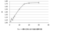
- FIG. 11 is a graph showing the relationship between the value of the ratio described at the rightmost of FIGS. 2 to 10 and the magnifying power in the wafer thickness direction.
- One aspect of the present invention is an evaluation method of a semiconductor wafer, wherein acquiring a cross-sectional image of a semiconductor wafer to be evaluated, the cross-sectional image includes a chamfered surface of the wafer outer peripheral edge and a wafer adjacent to the chamfered surface.
- a semiconductor including: forming an enlarged image obtained by enlarging the acquired cross-sectional image only in the wafer thickness direction, including a boundary with the surface; and evaluating the shape of the boundary in the generated enlarged image.
- the present invention relates to a wafer evaluation method.
- the shape of the boundary is evaluated using an enlarged image obtained by enlarging a cross-sectional image including the boundary between the chamfered surface of the semiconductor wafer and the wafer surface only in the wafer thickness direction.
- the cross-sectional shape of a plurality of semiconductor wafers is compared by a cross-sectional image acquired at an imaging magnification of 1 ⁇ vertical and horizontal magnifications, even if the difference in boundary portions is hardly seen, the difference in shape of the boundary portions of the plurality of semiconductor wafers Because of this, it is possible to distinguish slight differences in the shape of the boundary.
- the shape of the boundary between the chamfered surface of the semiconductor wafer and the wafer surface is evaluated by a simple image processing in which the cross-sectional image is enlarged only in the wafer thickness direction without going through complicated steps. can do. The above evaluation method will be described in more detail below.
- the semiconductor wafer to be evaluated by the above evaluation method may be a semiconductor wafer having a chamfered surface formed by chamfering the outer peripheral edge portion of the wafer.
- the semiconductor wafer to be evaluated can be various semiconductor wafers generally used as a semiconductor substrate.
- various silicon wafers can be mentioned as a specific example of a semiconductor wafer.
- the silicon wafer can be, for example, a silicon single crystal wafer cut out from a silicon single crystal ingot and then subjected to various processes such as chamfering.
- a specific example of such a silicon single crystal wafer there can be mentioned, for example, a polished wafer which has been subjected to polishing and has a polished surface on the surface.
- the silicon wafer can also be various silicon wafers such as an epitaxial wafer having an epitaxial layer on a silicon single crystal wafer, and an annealed wafer in which a modified layer is formed on a silicon single crystal wafer by annealing.
- a cross-sectional image of a semiconductor wafer to be evaluated is acquired.
- the cross-sectional image may be acquired so as to include the chamfered surface and the boundary between the chamfered surface and the wafer surface (front or back surface) adjacent to the chamfered surface.
- a chamfered surface adjacent to the front surface of the wafer and a chamfered surface adjacent to the back surface of the wafer are generally present.
- the cross-sectional image may include one or both of the boundary between the front surface and the chamfered surface of the wafer and the boundary between the back surface of the wafer and the chamfered surface.
- the cross-sectional image can be acquired as a projection image in one aspect without exposing the cross section of the semiconductor wafer to be evaluated.
- the projection image can be acquired by a known projection method.
- the cross-sectional image can be acquired by exposing the cross section of the semiconductor wafer to be evaluated and imaging the exposed cross section.
- the cross section can be exposed by cleaving the semiconductor wafer to be evaluated or by cutting it by a known cutting means.
- the cross-section is preferably a cleavage plane exposed by cleaving the semiconductor wafer to be evaluated perpendicularly to the surface.
- a cleavage plane perpendicular to the surface can be exposed by cleaving at the (110) plane.
- various known microscopes such as an optical microscope, a scanning electron microscope (SEM; Scanning Electron Microscope), and a laser microscope can be used.
- an optical microscope preferably, an optical metallographic microscope (referred to as an epi-illumination microscope or the like) can be used.
- using a differential interference microscope further provided with a differential interference observation function is more preferable because the depth of focus becomes shallow and a slight difference in shape also appears in the cross-sectional image.
- the cross-sectional image may be acquired with an imaging magnification of 1 ⁇ (ie, in the actual size), or may be acquired by enlarging the imaging magnification of over 1 ⁇ .
- the imaging magnification can be, for example, 50 to 1000 times, and preferably 50 to 500 times.
- the magnification is performed with equal magnification in any direction, as performed by the magnifying function provided in a known microscope.
- the cross-sectional image thus acquired is enlarged only in the wafer thickness direction (so-called vertical direction), and an enlarged image is created without being enlarged in the wafer radial direction (so-called horizontal direction).
- the shape of the boundary between the wafer surface and the chamfered surface can be evaluated with high accuracy.
- the creation of an enlarged image in which the cross-sectional image is enlarged only in the wafer thickness direction can be performed using known image processing software capable of enlarging the image.
- the magnifying power in the wafer thickness direction is more than 1 ⁇ , and can be, for example, 2 ⁇ or 3 ⁇ .
- the enlargement magnification in the wafer thickness direction is preferably 4 times or more, more preferably 5 times or more, and 6 times or more More preferably, it is more preferably 7 times or more, and still more preferably 8 times or more.
- the enlargement magnification in the wafer thickness direction can be, for example, 30 times or less, 25 times or less, or 20 times or less, and can also be 19 times or less, 18 times or less, 17 times or less, or 16 times or less. From the viewpoint of evaluating the shape of the boundary between the wafer surface and the chamfered surface more accurately, it is preferably 15 times or less, more preferably 14 times or less, and still more preferably 13 times or less, It is more preferable to make it 12 times or less.
- the obtained image may be binarized before or after the cross-sectional image is enlarged only in the wafer thickness direction.
- the obtained image is binarized. Since the contour of the cross-sectional shape can be displayed more clearly by performing the binarization processing, the shape of the boundary between the wafer surface and the chamfered surface can be evaluated more accurately.
- the binarization process is a process of converting a light and shade image into two gradations of white and black, and is performed with a certain threshold set.
- the threshold value in the binarization processing may be appropriately set so that the contour of the cross-sectional shape is clearly displayed.
- the shape of the boundary between the wafer surface and the chamfered surface adjacent to the wafer surface is evaluated in the magnified image enlarged only in the wafer thickness direction as described above.
- This shape evaluation can be performed as a relative evaluation, for example, by visually comparing magnified images obtained for a plurality of different semiconductor wafers. For example, it is relatively evaluated by visual observation whether the shape of the boundary is more gentle or steep in the created magnified image, and the boundary between the wafer surface of the semiconductor wafer to be evaluated and the chamfered surface The shape of the part can be evaluated.
- the boundary between the wafer surface and the chamfered surface of the semiconductor wafer to be evaluated by visually comparing the magnified image of the standard sample having the desired boundary shape and the magnified image created for the semiconductor wafer to be evaluated. It is also possible to evaluate the shape of the part.
- the plurality of magnified images to be compared are magnified images magnified at the same magnification only in the wafer thickness direction. That is, the evaluation of the boundary portion of the semiconductor wafer to be evaluated is preferably performed by comparing the enlarged image created for the wafer to be evaluated with one or more enlarged images to be compared.
- This comparative target magnified image acquires a cross-sectional image including the chamfered surface of the wafer outer peripheral edge of the semiconductor wafer to be compared and the boundary portion between the chamfered surface and the wafer surface adjacent to this chamfered surface. It is preferable that it is a magnified image created by magnifying at the same magnification as the magnified image of the semiconductor wafer to be evaluated only in the thickness direction.
- the shape of the boundary between the wafer surface and the chamfered surface usually has a curved shape in the contour of the wafer cross-sectional shape. Therefore, the shape of the boundary can also be evaluated based on the curvature circle of this curve. Specifically, on the outline of the wafer cross-sectional shape of an enlarged image expanded only in the wafer thickness direction, a circle having an arc shape approximate to the shape of this curve is fitted to the shape of the curve at the boundary between the wafer surface and the chamfered surface. Or, the shape of the curve at the boundary between the wafer surface and the chamfered surface is fitted with a circle having an arc shape that matches the shape of this curve.
- the fitting of this circle does not necessarily have to be an accurate circle fitting using a fitting equation.
- an arc having a shape that matches or approximates the shape of the curve of the boundary portion on the contour of the wafer cross-sectional shape using known software capable of manually drawing a circle. You can set a circle with.
- circle fitting may be performed using image processing software using a known fitting formula.
- the shape of the boundary between the surface and the chamfered surface can be judged to be steep.
- the shape of the boundary portion between the wafer front surface (front or back surface) of the semiconductor wafer and the chamfered surface adjacent to the front surface is a complicated process. Can easily be evaluated without going through the Furthermore, according to the evaluation method according to one aspect of the present invention, in the contour of the cross-sectional shape of the semiconductor wafer to be evaluated, the difference in the shape of the boundary with respect to the wafer surface can be emphasized. It becomes possible to evaluate the height / steepness with high accuracy.
- a method of manufacturing a semiconductor wafer (a first manufacturing method) according to an aspect of the present invention, Producing semiconductor wafer lots including multiple semiconductor wafers, Extracting at least one semiconductor wafer from the semiconductor wafer lot, Evaluating the extracted semiconductor wafer by the above evaluation method, and subjecting the semiconductor wafer of the same semiconductor wafer lot as the semiconductor wafer determined to be non-defective as a result of the evaluation to be shipped as a product semiconductor wafer, Of manufacturing a semiconductor wafer including It is.
- a method of manufacturing a semiconductor wafer is Manufacturing a semiconductor wafer for evaluation under test manufacturing conditions, Evaluating the manufactured semiconductor wafer for evaluation by the evaluation method; Based on the result of the evaluation, determining as the actual manufacturing condition the manufacturing condition in which the test manufacturing condition is changed or determining the test manufacturing condition as the actual manufacturing condition Manufacturing a semiconductor wafer under the above determined actual manufacturing conditions, Of manufacturing a semiconductor wafer including It is.
- the semiconductor wafer of the same lot as the semiconductor wafer determined to be non-defective as a result of the so-called sampling inspection is subjected to preparation for shipping as a product semiconductor wafer.
- the second manufacturing method semiconductor wafers manufactured under test manufacturing conditions are evaluated, and actual manufacturing conditions are determined based on the evaluation results.
- the evaluation of the semiconductor wafer is performed by the evaluation method according to one aspect of the present invention described above. Therefore, the semiconductor wafer can be easily evaluated, and furthermore, can be evaluated with high accuracy.
- a polished wafer which is one aspect of a silicon wafer, is obtained by cutting (slicing), chamfering, roughing (for example, lapping) a silicon wafer from a silicon single crystal ingot grown by the Czochralski method (CZ method) or the like. It can be manufactured by a manufacturing process including etching, mirror surface polishing (finishing polishing), and cleaning performed between the processing steps or after the processing steps. Also, the annealed wafer can be manufactured by annealing the polished wafer manufactured as described above.
- the epitaxial wafer can be manufactured by vapor phase growing (epitaxial growth) an epitaxial layer on the surface of the polished wafer manufactured as described above.
- the total number of semiconductor wafers included in the semiconductor wafer lot is not particularly limited.
- the number of semiconductor wafers extracted from the manufactured semiconductor wafer lot and subjected to so-called sampling inspection is at least one, and may be two or more, and the number is not particularly limited.
- the shape of the boundary between the wafer surface and the chamfered surface adjacent to the wafer surface is evaluated for the semiconductor wafer extracted from the semiconductor wafer lot by the evaluation method according to one aspect of the present invention.
- the details of the evaluation method are as described above.
- the semiconductor wafer of the same semiconductor wafer lot as the semiconductor wafer determined to be non-defective as a result of the evaluation is prepared for shipping as a product semiconductor wafer.
- the criteria for determining a non-defective product may be determined according to the quality required for the product semiconductor wafer.
- the size of a circle created by fitting a circle to the shape of the boundary between the wafer surface and the chamfered surface as described above is equal to or greater than a certain value (that is, greater than or equal to a threshold). It can be used as a reference for determination.
- the shape of the boundary portion of the standard sample and the evaluation are evaluated by visually comparing the enlarged image of the standard sample having the desired boundary shape with the enlarged image of the semiconductor wafer to be evaluated extracted from the semiconductor wafer lot. It can also be judged as non-defective by visually judging that the shape of the boundary portion of the target semiconductor wafer is similar.
- one or more semiconductor wafers in the same lot as the semiconductor wafers determined to be non-defective are subjected to preparation for shipment as product semiconductor wafers.
- packing etc. can be mentioned, for example.
- test manufacturing conditions and the actual manufacturing conditions various conditions in various steps for manufacturing a semiconductor wafer can be mentioned.
- the various steps for manufacturing the semiconductor wafer are as described above for the first manufacturing method.
- the actual manufacturing conditions shall mean the manufacturing conditions of a product semiconductor wafer.
- test manufacturing conditions are set as a preliminary step for determining actual manufacturing conditions, and a semiconductor wafer for evaluation is manufactured under the test manufacturing conditions.
- the shape of the boundary between the wafer surface and the chamfered surface adjacent to the surface is evaluated by the evaluation method according to one aspect of the present invention.
- the details of the evaluation method are as described above.
- the number of semiconductor wafers for evaluation is at least one, and may be two or more, and the number thereof is not particularly limited.
- the manufacturing conditions in which the test manufacturing conditions are changed Determined as manufacturing conditions.
- the manufacturing conditions to be changed are preferably manufacturing conditions that are considered to affect the shape of the boundary between the wafer surface and the chamfered surface.
- polishing conditions of the front surface (front side and / or back side) of a semiconductor wafer can be mentioned.
- polishing conditions rough polishing conditions and mirror polishing conditions can be mentioned, and more specifically, types of polishing solution, concentration of abrasive particles in the polishing solution, types of polishing pad (eg hardness, etc.) It can be mentioned.
- chamfering conditions can be mentioned, and in detail, machining conditions such as grinding and polishing in chamfering can be mentioned, and more specifically, types of polishing tapes used for chamfering Etc. can be mentioned.
- the manufacturing conditions in which the test manufacturing conditions are changed are determined as the actual manufacturing conditions, and the product semiconductor wafer is manufactured and shipped under the actual manufacturing conditions, so that the shapes of the wafer surface and the chamfered surface are desired shapes.
- Product semiconductor wafers can be stably mass-produced.
- the semiconductor wafer for evaluation is manufactured again under the manufacturing conditions in which the test manufacturing conditions are changed, and the semiconductor wafer for evaluation is evaluated by the evaluation method according to an aspect of the present invention, and the manufacturing conditions are referred to as actual manufacturing conditions. Determining whether to make a change or to make a change may be repeated once or more than once.
- the first manufacturing method is used to determine whether the shape of the boundary between the wafer surface and the chamfered surface of the semiconductor wafer for evaluation is the shape desired for the product semiconductor wafer.
- the description on determination of non-defective items of the method can be referred to.
- the cross-sectional image (imaging magnification: the boundary between the surface (front surface) of the wafer and the adjacent chamfered surface is adjusted by adjusting the brightness and contrast using the differential interference microscope to prepare the cross-sectional observation sample prepared in Obtained 500 times).
- the acquired cross-sectional image is shown in FIG.
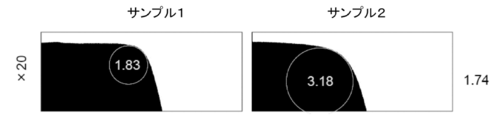
- FIGS. 3 to 10 Magnified images after binarization processing are shown in FIGS. 3 to 10. In FIG. The cross-sectional image acquired by these is shown the binarized image which performed only the binarization process like the above without expanding.
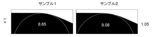
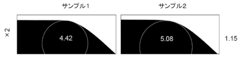
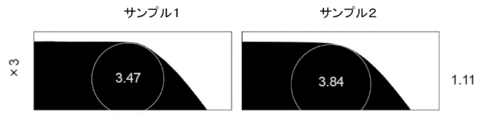
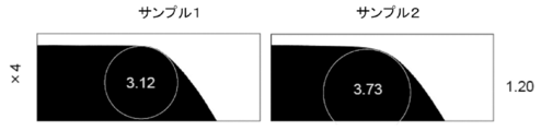
- FIG. 3 shows a magnified image magnified at a magnification of 2 ⁇ only in the wafer thickness direction, “ ⁇ 2” is written on the far left of FIG. The above 3. Since the binarized image of the cross-sectional image (without enlargement) acquired in the above is shown, “ ⁇ 1” is described at the leftmost of FIG. 1. On the other hand, in FIGS. 2 to 10, the numerical values described on the far right are the ratio of the diameter of the circle drawn for sample 2 to the diameter of the circle drawn for sample 1 (the circle of sample 2 drawn Diameter / diameter of circle drawn for sample 1).
- FIG. 11 is a graph showing the relationship between the value of the ratio described at the rightmost in FIGS. 2 to 10 and the magnifying power in the wafer thickness direction. From the graph of FIG. 11, it can be confirmed that the value of the ratio monotonously increases when the magnification is 4 or more. Further, it can be confirmed from the graph of FIG. 11 that the degree of increase in the ratio value decreases when the enlargement ratio exceeds 15 times. Also, in the magnified image at 20 times (FIG.
- the enlargement ratio in the wafer thickness direction is preferably 15 or less. From the above results, it can be judged that the enlargement magnification in the wafer thickness direction is preferably 4 times or more and 15 times or less.
- the shape of the boundary between the wafer surface and the chamfered surface can be easily evaluated. It was confirmed that the differences could also be evaluated accurately.
- the results of such an evaluation can be used for lot inspection, as described above, and can also be used to determine the actual manufacturing conditions of semiconductor wafers.
- the present invention is useful in the field of manufacturing various semiconductor wafers such as silicon wafers.
Landscapes
- Physics & Mathematics (AREA)
- Engineering & Computer Science (AREA)
- General Physics & Mathematics (AREA)
- Computer Vision & Pattern Recognition (AREA)
- Theoretical Computer Science (AREA)
- General Engineering & Computer Science (AREA)
- Probability & Statistics with Applications (AREA)
- Quality & Reliability (AREA)
- Testing Or Measuring Of Semiconductors Or The Like (AREA)
- Mechanical Treatment Of Semiconductor (AREA)
- Length Measuring Devices By Optical Means (AREA)
Abstract
半導体ウェーハの評価方法であって、評価対象の半導体ウェーハの断面像を取得すること、上記断面像はウェーハ外周縁部の面取り面とこの面取り面と隣接するウェーハ表面との境界部を含み、上記取得された断面像をウェーハ厚み方向のみに拡大した拡大像を作成すること、上記作成された拡大像において、上記境界部の形状を評価することを含む半導体ウェーハの評価方法が提供される。
Description
本発明は、半導体ウェーハの評価方法および半導体ウェーハの製造方法に関する。
近年、半導体ウェーハについて、ウェーハ外周縁部を含むウェーハの断面形状を評価することが行われている(例えば特許文献1参照)。
特許文献1には、ウェーハの断面像から表面輪郭の座標列を求め、これを数学的座標系で曲線に表現することにより、曲線を数学的に処理してウェーハの形状に関する形状分析データを数値化して表現することが提案されている(特許文献1の段落0032等参照)。
ところで、半導体ウェーハは、一般に、インゴットから切り出したウェーハに各種加工を施して製造される。インゴットから切り出したウェーハの外周縁部は、そのままでは角部を有するため割れや欠けが生じやすい。そこで、ウェーハの外周縁部に面取り加工を施し面取り面を形成することが通常行われる。
面取り面が形成された半導体ウェーハの断面像を取得することにより、その断面像において、半導体ウェーハのデバイス形成面となる表面(おもて面)またはおもて面とは反対側の表面(裏面)と面取り面との境界部の形状を観察することができる。以下において、半導体ウェーハの「表面」とは、特記しない限り、上記のおもて面または裏面のいずれか一方または両方を言うものする。ウェーハ表面と面取り面との境界部の形状は、半導体デバイスの製造工程における欠け、キズの発生のし易さ等を予測するための指標とすることができる。例えば、半導体デバイスの製造工程において、熱処理時にウェーハを支持するウェーハサポートの形状に合わせてウェーハ表面(例えば裏面)と面取り面との境界部の形状を適切に設定することによって、接触による境界部の欠けやキズが発生し難くなるため、欠けやキズを原因とする転位(スリップ)や発塵の発生率を低減することができる。しかし、特許文献1に記載の方法は、ウェーハの形状を数値化するための工程が複雑であるため、より簡便な評価方法によってウェーハ表面と面取り面との境界部の形状を評価できることが望ましい。
そこで本発明の目的は、半導体ウェーハのウェーハ表面と面取り面との境界部の形状を簡便に評価するための新たな方法を提供することにある。
本発明の一態様は、
半導体ウェーハの評価方法であって、
評価対象の半導体ウェーハの断面像を取得すること、
上記断面像は、ウェーハ外周縁部の面取り面と、この面取り面と隣接するウェーハ表面との境界部を含み、
上記取得された断面像をウェーハ厚み方向のみに拡大した拡大像を作成すること、
上記作成された拡大像において、上記境界部の形状を評価すること、
を含む半導体ウェーハの評価方法(以下、「評価方法」とも記載する。)、
に関する。
半導体ウェーハの評価方法であって、
評価対象の半導体ウェーハの断面像を取得すること、
上記断面像は、ウェーハ外周縁部の面取り面と、この面取り面と隣接するウェーハ表面との境界部を含み、
上記取得された断面像をウェーハ厚み方向のみに拡大した拡大像を作成すること、
上記作成された拡大像において、上記境界部の形状を評価すること、
を含む半導体ウェーハの評価方法(以下、「評価方法」とも記載する。)、
に関する。
一態様では、上記断面像は、評価対象の半導体ウェーハをへき開して露出させたへき開面において撮像された断面像であることができる。
一態様では、上記拡大像は、上記取得された断面像をウェーハ厚み方向のみに4倍以上の拡大倍率で拡大させて作成された拡大像であることができる。
一態様では、上記拡大倍率は、4倍以上15倍以下であることができる。
一態様では、上記評価に用いる拡大像は、上記拡大後に二値化処理が行われた像であることができる。
一態様では、上記評価は、上記拡大像において上記境界部の形状に円をフィッティングさせて作成した円のサイズを指標として行うことができる。
一態様では、評価対象の半導体ウェーハの上記境界部の評価を、上記作成された拡大像と比較対象拡大像と対比することにより行うことができる。この比較対象拡大像は、比較対象の半導体ウェーハのウェーハ外周縁部の面取り面とこの面取り面と隣接するウェーハ表面との境界部を含む断面像を取得し、この取得された断面像を、ウェーハ厚み方向のみに、上記評価対象の半導体ウェーハの拡大像と同じ拡大倍率で拡大して作成された拡大像であることができる。
本発明の更なる態様は、
複数の半導体ウェーハを含む半導体ウェーハロットを製造すること、
上記半導体ウェーハロットから少なくとも1つの半導体ウェーハを抽出すること、
上記抽出された半導体ウェーハを上記評価方法によって評価すること、および
上記評価の結果、良品と判定された半導体ウェーハと同じ半導体ウェーハロットの半導体ウェーハを製品半導体ウェーハとして出荷するための準備に付すこと、
を含む半導体ウェーハの製造方法(以下、「第一の製造方法」とも記載する。)、
に関する。
複数の半導体ウェーハを含む半導体ウェーハロットを製造すること、
上記半導体ウェーハロットから少なくとも1つの半導体ウェーハを抽出すること、
上記抽出された半導体ウェーハを上記評価方法によって評価すること、および
上記評価の結果、良品と判定された半導体ウェーハと同じ半導体ウェーハロットの半導体ウェーハを製品半導体ウェーハとして出荷するための準備に付すこと、
を含む半導体ウェーハの製造方法(以下、「第一の製造方法」とも記載する。)、
に関する。
本発明の更なる態様は、
テスト製造条件下で評価用半導体ウェーハを製造すること、
上記製造された評価用半導体ウェーハを上記評価方法によって評価すること、
上記評価の結果に基づき、上記テスト製造条件に変更を加えた製造条件を実製造条件として決定するか、または上記テスト製造条件を実製造条件として決定すること、
上記決定された実製造条件下で半導体ウェーハを製造すること、
を含む半導体ウェーハの製造方法(以下、「第二の製造方法」とも記載する。)、
に関する。
テスト製造条件下で評価用半導体ウェーハを製造すること、
上記製造された評価用半導体ウェーハを上記評価方法によって評価すること、
上記評価の結果に基づき、上記テスト製造条件に変更を加えた製造条件を実製造条件として決定するか、または上記テスト製造条件を実製造条件として決定すること、
上記決定された実製造条件下で半導体ウェーハを製造すること、
を含む半導体ウェーハの製造方法(以下、「第二の製造方法」とも記載する。)、
に関する。
一態様では、上記変更が加えられる製造条件は、半導体ウェーハ表面の研磨処理条件および面取り加工条件の少なくとも一方であることができる。
本発明の一態様によれば、半導体ウェーハの面取り面とウェーハ表面との境界部の形状を簡便に評価することができる評価方法を提供することができる。
[半導体ウェーハの評価方法]
本発明の一態様は、半導体ウェーハの評価方法であって、評価対象の半導体ウェーハの断面像を取得すること、上記断面像は、ウェーハ外周縁部の面取り面と、この面取り面と隣接するウェーハ表面との境界部を含み、上記取得された断面像をウェーハ厚み方向のみに拡大した拡大像を作成すること、上記作成された拡大像において、上記境界部の形状を評価すること、を含む半導体ウェーハの評価方法に関する。
本発明の一態様は、半導体ウェーハの評価方法であって、評価対象の半導体ウェーハの断面像を取得すること、上記断面像は、ウェーハ外周縁部の面取り面と、この面取り面と隣接するウェーハ表面との境界部を含み、上記取得された断面像をウェーハ厚み方向のみに拡大した拡大像を作成すること、上記作成された拡大像において、上記境界部の形状を評価すること、を含む半導体ウェーハの評価方法に関する。
上記評価方法では、半導体ウェーハの面取り面とウェーハ表面との境界部を含む断面像を、ウェーハ厚み方向のみに拡大した拡大像を用いて境界部の形状を評価する。ウェーハ厚み方向のみに断面像を拡大することにより、断面形状の輪郭において、半導体ウェーハの境界部の形状の違いをウェーハ表面(いわゆる水平面)に対して強調することができるため、境界部のなだらかさ/急峻さを精度よく評価することが可能となる。したがって、例えば、複数の半導体ウェーハの断面形状を縦横等倍の撮影倍率で取得された断面像により比較すると境界部の違いがほぼ見られない場合でも、複数の半導体ウェーハの境界部の形状の違いを強調することができるため、わずかな境界部の形状の違いも判別することができる。また、上記評価方法によれば、複雑な工程を経ることなく、断面像をウェーハ厚み方向のみに拡大するという簡便な画像処理により、半導体ウェーハの面取り面とウェーハ表面との境界部の形状を評価することができる。
以下、上記評価方法について、更に詳細に説明する。
以下、上記評価方法について、更に詳細に説明する。
<評価対象の半導体ウェーハ>
上記評価方法の評価対象の半導体ウェーハは、ウェーハの外周縁部に面取り加工が施されて面取り面が形成された半導体ウェーハであればよい。評価対象の半導体ウェーハは、一般に半導体基板として使用される各種半導体ウェーハであることができる。例えば、半導体ウェーハの具体例としては、各種シリコンウェーハを挙げることができる。シリコンウェーハは、例えば、シリコン単結晶インゴットから切り出された後に面取り加工等の各種加工を経たシリコン単結晶ウェーハであることができる。かかるシリコン単結晶ウェーハの具体例としては、例えば、研磨が施されて表面に研磨面を有するポリッシュドウェーハを挙げることができる。また、シリコンウェーハは、シリコン単結晶ウェーハ上にエピタキシャル層を有するエピタキシャルウェーハ、シリコン単結晶ウェーハにアニール処理により改質層を形成したアニールウェーハ等の各種シリコンウェーハであることもできる。
上記評価方法の評価対象の半導体ウェーハは、ウェーハの外周縁部に面取り加工が施されて面取り面が形成された半導体ウェーハであればよい。評価対象の半導体ウェーハは、一般に半導体基板として使用される各種半導体ウェーハであることができる。例えば、半導体ウェーハの具体例としては、各種シリコンウェーハを挙げることができる。シリコンウェーハは、例えば、シリコン単結晶インゴットから切り出された後に面取り加工等の各種加工を経たシリコン単結晶ウェーハであることができる。かかるシリコン単結晶ウェーハの具体例としては、例えば、研磨が施されて表面に研磨面を有するポリッシュドウェーハを挙げることができる。また、シリコンウェーハは、シリコン単結晶ウェーハ上にエピタキシャル層を有するエピタキシャルウェーハ、シリコン単結晶ウェーハにアニール処理により改質層を形成したアニールウェーハ等の各種シリコンウェーハであることもできる。
<断面像の取得>
上記評価方法では、評価対象の半導体ウェーハの断面像を取得する。この断面像は、面取り面と、この面取り面と隣接するウェーハ表面(おもて面または裏面)との境界部を含むように取得すればよい。面取り加工された半導体ウェーハの外周縁部には、通常、ウェーハのおもて面と隣接する面取り面と、ウェーハの裏面と隣接する面取り面が存在する。断面像には、ウェーハのおもて面と面取り面との境界部、ウェーハの裏面と面取り面との境界部の一方または両方が含まれ得る。
上記評価方法では、評価対象の半導体ウェーハの断面像を取得する。この断面像は、面取り面と、この面取り面と隣接するウェーハ表面(おもて面または裏面)との境界部を含むように取得すればよい。面取り加工された半導体ウェーハの外周縁部には、通常、ウェーハのおもて面と隣接する面取り面と、ウェーハの裏面と隣接する面取り面が存在する。断面像には、ウェーハのおもて面と面取り面との境界部、ウェーハの裏面と面取り面との境界部の一方または両方が含まれ得る。
断面像は、一態様では、評価対象の半導体ウェーハの断面を露出させることなく、投影像として取得することができる。投影像は、公知の投影法によって取得することができる。また、他の一態様では、断面像は、評価対象の半導体ウェーハの断面を露出させ、この露出させた断面を撮像して取得することができる。例えば評価対象の半導体ウェーハをへき開するか、または公知の切断手段によって切断することにより、断面を露出させることができる。断面露出の容易性の観点からは、上記断面は、評価対象の半導体ウェーハを表面に対して垂直にへき開して露出させたへき開面であることが好ましい。例えば、表面が(100)面であるシリコン単結晶ウェーハであれば、(110)面でへき開することにより、表面に対して垂直なへき開面を露出させることができる。露出させた断面の撮像には、光学顕微鏡、走査型電子顕微鏡(SEM;Scanning Electron Microscope)、レーザー顕微鏡等の公知の各種顕微鏡を用いることができる。光学顕微鏡としては、好ましくは光学式の金属顕微鏡(落射照明型顕微鏡等と呼ばれる。)を用いることができる。また、微分干渉観察機能を更に備えた微分干渉顕微鏡を用いると、焦点深度が浅くなり、わずかな形状の違いも断面像に現れるため、より好ましい。
断面像は、撮像倍率を1倍として(即ち実サイズで)取得してもよく、撮像倍率を1倍超として拡大して取得してもよい。拡大する場合、撮像倍率は、例えば50~1000倍とすることができ、50~500倍とすることが好ましい。ただし、ここでの拡大では、公知の顕微鏡に備えられた拡大機能により行われる通り、いずれの方向においても等しい倍率で行われる。そして上記評価方法では、こうして取得された断面像を、ウェーハ厚み方向(いわゆる縦方向)のみに拡大し、ウェーハ径方向(いわゆる横方向)には拡大せずに、拡大像を作成する。このようにウェーハ厚み方向のみに拡大した拡大像を用いることにより、ウェーハ表面と面取り面との境界部の形状を精度よく評価することができる。
<拡大像の作成>
上記断面像をウェーハ厚み方向のみに拡大した拡大像の作成は、画像を拡大することができる公知の画像処理ソフトを使用して行うことができる。ウェーハ厚み方向での拡大倍率は、1倍超であり、例えば2倍以上または3倍以上とすることができる。ウェーハ表面と面取り面との形状をより精度よく評価する観点からは、ウェーハ厚み方向での拡大倍率は4倍以上とすることが好ましく、5倍以上とすることがより好ましく、6倍以上とすることが更に好ましく、7倍以上とすることが一層好ましく、8倍以上とすることがより一層好ましい。また、ウェーハ厚み方向での拡大倍率は、例えば30倍以下、25倍以下または20倍以下とすることができ、19倍以下、18倍以下、17倍以下または16倍以下とすることもできる。ウェーハ表面と面取り面との境界部の形状をより精度よく評価する観点からは、15倍以下とすることが好ましく、14倍以下とすることがより好ましく、13倍以下とすることが更に好ましく、12倍以下とすることが一層好ましい。
上記断面像をウェーハ厚み方向のみに拡大した拡大像の作成は、画像を拡大することができる公知の画像処理ソフトを使用して行うことができる。ウェーハ厚み方向での拡大倍率は、1倍超であり、例えば2倍以上または3倍以上とすることができる。ウェーハ表面と面取り面との形状をより精度よく評価する観点からは、ウェーハ厚み方向での拡大倍率は4倍以上とすることが好ましく、5倍以上とすることがより好ましく、6倍以上とすることが更に好ましく、7倍以上とすることが一層好ましく、8倍以上とすることがより一層好ましい。また、ウェーハ厚み方向での拡大倍率は、例えば30倍以下、25倍以下または20倍以下とすることができ、19倍以下、18倍以下、17倍以下または16倍以下とすることもできる。ウェーハ表面と面取り面との境界部の形状をより精度よく評価する観点からは、15倍以下とすることが好ましく、14倍以下とすることがより好ましく、13倍以下とすることが更に好ましく、12倍以下とすることが一層好ましい。
ウェーハ表面と面取り面との境界部の形状をより一層精度よく評価する観点からは、断面像をウェーハ厚み方向のみに拡大する前または拡大した後に、得られた画像を二値化処理することが好ましく、断面像をウェーハ厚み方向のみに拡大した後に、得られた画像を二値化処理することがより好ましい。二値化処理することにより、断面形状の輪郭をより鮮明に表示させることができるため、ウェーハ表面と面取り面との境界部の形状をより一層精度よく評価することが可能となる。二値化処理は、公知の通り、濃淡のある画像を白と黒との2階調に変換する処理であり、ある閾値を定めて行われる。上記評価方法において二値化処理された断面像を評価に用いる場合、二値化処理における閾値は、断面形状の輪郭が鮮明に表示されるように適宜設定すればよい。
<境界部の形状の評価>
上記評価方法では、以上のようにウェーハ厚み方向のみに拡大した拡大像において、ウェーハ表面と、この表面と隣接する面取り面との境界部の形状を評価する。この形状の評価は、例えば、複数の異なる半導体ウェーハについて得られた拡大像を目視で対比して、相対評価として行うことができる。例えば、作成された拡大像において境界部の形状が、よりなだらかであるか、またはより急峻であるかを目視により相対的に評価して、評価対象の半導体ウェーハのウェーハ表面と面取り面との境界部の形状を評価することができる。また、例えば、所望の境界部形状を有する標準サンプルの拡大像と評価対象の半導体ウェーハについて作成された拡大像とを目視で対比して、評価対象の半導体ウェーハのウェーハ表面と面取り面との境界部の形状を評価することもできる。以上の評価において、対比する複数の拡大像は、ウェーハ厚み方向のみに同じ倍率で拡大された拡大像であることが、評価の精度の観点から好ましい。即ち、評価対象の半導体ウェーハの境界部の評価は、評価対象ウェーハについて作成された拡大像と、1つ以上の比較対象拡大像と対比することにより行うことが好ましい。この比較対象拡大像は、比較対象の半導体ウェーハのウェーハ外周縁部の面取り面とこの面取り面と隣接するウェーハ表面との境界部を含む断面像を取得し、この取得された断面像を、ウェーハ厚み方向のみに、評価対象の半導体ウェーハの拡大像と同じ拡大倍率で拡大して作成された拡大像であることが好ましい。
上記評価方法では、以上のようにウェーハ厚み方向のみに拡大した拡大像において、ウェーハ表面と、この表面と隣接する面取り面との境界部の形状を評価する。この形状の評価は、例えば、複数の異なる半導体ウェーハについて得られた拡大像を目視で対比して、相対評価として行うことができる。例えば、作成された拡大像において境界部の形状が、よりなだらかであるか、またはより急峻であるかを目視により相対的に評価して、評価対象の半導体ウェーハのウェーハ表面と面取り面との境界部の形状を評価することができる。また、例えば、所望の境界部形状を有する標準サンプルの拡大像と評価対象の半導体ウェーハについて作成された拡大像とを目視で対比して、評価対象の半導体ウェーハのウェーハ表面と面取り面との境界部の形状を評価することもできる。以上の評価において、対比する複数の拡大像は、ウェーハ厚み方向のみに同じ倍率で拡大された拡大像であることが、評価の精度の観点から好ましい。即ち、評価対象の半導体ウェーハの境界部の評価は、評価対象ウェーハについて作成された拡大像と、1つ以上の比較対象拡大像と対比することにより行うことが好ましい。この比較対象拡大像は、比較対象の半導体ウェーハのウェーハ外周縁部の面取り面とこの面取り面と隣接するウェーハ表面との境界部を含む断面像を取得し、この取得された断面像を、ウェーハ厚み方向のみに、評価対象の半導体ウェーハの拡大像と同じ拡大倍率で拡大して作成された拡大像であることが好ましい。
また、ウェーハ厚み方向のみに拡大した拡大像において、ウェーハ断面形状の輪郭では、通常、ウェーハ表面と面取り面との境界部の形状は曲線形状となる。そこで、この曲線の曲率円に基づき、境界部の形状を評価することもできる。詳しくは、ウェーハ厚み方向のみに拡大した拡大像のウェーハ断面形状の輪郭上で、ウェーハ表面と面取り面との境界部の曲線の形状に、この曲線の形状に近似する円弧形状を有する円をフィッティングさせるか、またはウェーハ表面と面取り面との境界部の曲線の形状に、この曲線の形状と一致する円弧形状を有する円をフィッティングさせる。この円のフィッティングは、必ずしもフィッティング式を用いた正確な円フィッティングでなくてもよい。例えば、ウェーハ厚み方向のみに拡大した拡大像において、手動での円の描画が可能な公知のソフトを用いて、ウェーハ断面形状の輪郭上の境界部の曲線の形状と一致または近似する形状の円弧を有する円を設定することができる。または、画像処理ソフトを用いて公知のフィッティング式を用いて円のフィッティングを行ってもよい。こうして得られた円(曲率円)のサイズ、例えば直径または半径が大きいほど、ウェーハ表面と面取り面との境界部の形状はなだらかであると判断することができ、上記円のサイズが小さいほどウェーハ表面と面取り面との境界部の形状は急峻であると判断することができる。このように円のサイズを用いて境界部の形状を評価することは、数値に基づき客観的に評価を行うことができるため、評価の信頼性の観点から好ましい。
以上の通り、本発明の一態様にかかる評価方法によれば、半導体ウェーハのウェーハ表面(おもて面または裏面)と、この表面と隣接する面取り面との境界部の形状を、複雑な工程を経ることなく簡便に評価することができる。更に、本発明の一態様にかかる評価方法によれば、評価対象の半導体ウェーハの断面形状の輪郭において、ウェーハ表面に対して境界部の形状の違いを強調することができるため、境界部のなだらかさ/急峻さを精度よく評価することが可能となる。
<半導体ウェーハの製造方法>
本発明の一態様にかかる半導体ウェーハの製造方法(第一の製造方法)は、
複数の半導体ウェーハを含む半導体ウェーハロットを製造すること、
上記半導体ウェーハロットから少なくとも1つの半導体ウェーハを抽出すること、
上記抽出された半導体ウェーハを上記評価方法によって評価すること、および
上記評価の結果、良品と判定された半導体ウェーハと同じ半導体ウェーハロットの半導体ウェーハを製品半導体ウェーハとして出荷するための準備に付すこと、
を含む半導体ウェーハの製造方法、
である。
本発明の一態様にかかる半導体ウェーハの製造方法(第一の製造方法)は、
複数の半導体ウェーハを含む半導体ウェーハロットを製造すること、
上記半導体ウェーハロットから少なくとも1つの半導体ウェーハを抽出すること、
上記抽出された半導体ウェーハを上記評価方法によって評価すること、および
上記評価の結果、良品と判定された半導体ウェーハと同じ半導体ウェーハロットの半導体ウェーハを製品半導体ウェーハとして出荷するための準備に付すこと、
を含む半導体ウェーハの製造方法、
である。
本発明の他の一態様にかかる半導体ウェーハの製造方法(第二の製造方法)は、
テスト製造条件下で評価用半導体ウェーハを製造すること、
上記製造された評価用半導体ウェーハを上記評価方法によって評価すること、
上記評価の結果に基づき、上記テスト製造条件に変更を加えた製造条件を実製造条件として決定するか、または上記テスト製造条件を実製造条件として決定すること、
上記決定された実製造条件下で半導体ウェーハを製造すること、
を含む半導体ウェーハの製造方法、
である。
テスト製造条件下で評価用半導体ウェーハを製造すること、
上記製造された評価用半導体ウェーハを上記評価方法によって評価すること、
上記評価の結果に基づき、上記テスト製造条件に変更を加えた製造条件を実製造条件として決定するか、または上記テスト製造条件を実製造条件として決定すること、
上記決定された実製造条件下で半導体ウェーハを製造すること、
を含む半導体ウェーハの製造方法、
である。
第一の製造方法では、いわゆる抜き取り検査を行った結果、良品と判定された半導体ウェーハと同じロットの半導体ウェーハを製品半導体ウェーハとして出荷するための準備に付す。一方、第二の製造方法では、テスト製造条件下で製造された半導体ウェーハを評価し、この評価結果に基づき実製造条件を決定する。第一の製造方法および第二の製造方法のいずれにおいても、半導体ウェーハの評価は、先に説明した本発明の一態様にかかる評価方法によって行われる。したがって、半導体ウェーハの評価を簡便に行うことができ、更には精度よく行うこともできる。
(第一の製造方法)
第一の製造方法における半導体ウェーハロットの製造は、一般的な半導体ウェーハの製造方法と同様に行うことができる。例えば、シリコンウェーハの一態様であるポリッシュドウェーハは、チョクラルスキー法(CZ法)等により育成されたシリコン単結晶インゴットからのシリコンウェーハの切断(スライシング)、面取り加工、粗研磨(例えばラッピング)、エッチング、鏡面研磨(仕上げ研磨)、上記加工工程間または加工工程後に行われる洗浄を含む製造工程により製造することができる。また、アニールウェーハは、上記のように製造されたポリッシュドウェーハにアニール処理を施して製造することができる。エピタキシャルウェーハは、上記のように製造されたポリッシュドウェーハの表面にエピタキシャル層を気相成長(エピタキシャル成長)させることにより製造することができる。半導体ウェーハロットに含まれる半導体ウェーハの総数は特に限定されるものではない。製造された半導体ウェーハロットから抜き出し、いわゆる抜き取り検査に付す半導体ウェーハの数は少なくとも1つであり、2つ以上であってもよく、その数は特に限定されるものではない。
第一の製造方法における半導体ウェーハロットの製造は、一般的な半導体ウェーハの製造方法と同様に行うことができる。例えば、シリコンウェーハの一態様であるポリッシュドウェーハは、チョクラルスキー法(CZ法)等により育成されたシリコン単結晶インゴットからのシリコンウェーハの切断(スライシング)、面取り加工、粗研磨(例えばラッピング)、エッチング、鏡面研磨(仕上げ研磨)、上記加工工程間または加工工程後に行われる洗浄を含む製造工程により製造することができる。また、アニールウェーハは、上記のように製造されたポリッシュドウェーハにアニール処理を施して製造することができる。エピタキシャルウェーハは、上記のように製造されたポリッシュドウェーハの表面にエピタキシャル層を気相成長(エピタキシャル成長)させることにより製造することができる。半導体ウェーハロットに含まれる半導体ウェーハの総数は特に限定されるものではない。製造された半導体ウェーハロットから抜き出し、いわゆる抜き取り検査に付す半導体ウェーハの数は少なくとも1つであり、2つ以上であってもよく、その数は特に限定されるものではない。
半導体ウェーハロットから抽出された半導体ウェーハは、本発明の一態様にかかる評価方法によって、ウェーハ表面と、この表面と隣接する面取り面との境界部の形状が評価される。評価方法の詳細は、先に記載した通りである。そして評価の結果、良品と判定された半導体ウェーハと同じ半導体ウェーハロットの半導体ウェーハを、製品半導体ウェーハとして出荷するための準備に付す。良品と判定するための基準は、製品半導体ウェーハに求められる品質に応じて決定すればよい。例えば一態様では、先に記載したようにウェーハ表面と面取り面との境界部の形状に円をフィッティングさせて作成した円のサイズが、ある値以上(即ち閾値以上)であることを、良品と判定するための基準とすることができる。または、所望の境界部形状を有する標準サンプルの拡大像と、半導体ウェーハロットから抜き出した評価対象の半導体ウェーハについて作成された拡大像とを目視で対比して、標準サンプルの境界部の形状と評価対象の半導体ウェーハの境界部の形状とが近似していることを目視で判断して、良品と判定することもできる。次いで、良品と判定された半導体ウェーハと同じロットの1つ以上の半導体ウェーハが、製品半導体ウェーハとして出荷するための準備に付される。この準備としては、例えば梱包等を挙げることができる。こうして第一の製造方法によれば、ウェーハ表面と面取り面との境界部の形状が製品半導体ウェーハに望まれる形状である半導体ウェーハを、安定的に量産することが可能となる。
(第二の製造方法)
第二の製造方法について、テスト製造条件および実製造条件としては、半導体ウェーハの製造のための各種工程における各種条件を挙げることができる。半導体ウェーハの製造のための各種工程については、先に第一の製造方法について記載した通りである。なお、「実製造条件」とは、製品半導体ウェーハの製造条件を意味するものとする。
第二の製造方法について、テスト製造条件および実製造条件としては、半導体ウェーハの製造のための各種工程における各種条件を挙げることができる。半導体ウェーハの製造のための各種工程については、先に第一の製造方法について記載した通りである。なお、「実製造条件」とは、製品半導体ウェーハの製造条件を意味するものとする。
第二の製造方法では、実製造条件を決定するための前段階として、テスト製造条件を設定し、このテスト製造条件下で評価用半導体ウェーハを製造する。製造された半導体ウェーハは、本発明の一態様にかかる評価方法によって、ウェーハ表面と、この表面と隣接する面取り面との境界部の形状が評価される。評価方法の詳細は、先に記載した通りである。評価用半導体ウェーハは、少なくとも1つであり、2つ以上であってもよく、その数は特に限定されるものではない。評価の結果、評価用半導体ウェーハのウェーハ表面と面取り面との境界部の形状が、製品半導体ウェーハに望まれる形状であれば、このテスト製造条件を実製造条件として製品半導体ウェーハを製造して出荷することにより、ウェーハ表面と面取り面との形状が所望の形状である製品半導体ウェーハを、安定的に量産することができる。他方、評価の結果、評価用半導体ウェーハのウェーハ表面と面取り面との境界部の形状が、製品半導体ウェーハに望まれる形状とは異なる場合には、テスト製造条件に変更を加えた製造条件を実製造条件として決定する。変更を加える製造条件は、ウェーハ表面と面取り面との境界部の形状に影響を及ぼすと考えられる製造条件であることが好ましい。そのような製造条件の一例としては、半導体ウェーハの表面(おもて面および/または裏面)の研磨条件を挙げることができる。かかる研磨条件の具体例としては、粗研磨条件および鏡面研磨条件を挙げることができ、より詳しくは、研磨液の種類、研磨液の砥粒濃度、研磨パットの種類(例えば硬さ等)等を挙げることができる。また、製造条件の一例としては、面取り加工条件を挙げることもでき、詳しくは、面取り加工における研削、研磨等の機械加工条件を挙げることができ、より詳しくは、面取り加工に用いる研磨テープの種類等を挙げることができる。こうしてテスト製造条件に変更を加えた製造条件を実製造条件として決定し、この実製造条件下で製品半導体ウェーハを製造し出荷することにより、ウェーハ表面と面取り面との形状が所望の形状である製品半導体ウェーハを、安定的に量産することができる。なおテスト製造条件に変更を加えた製造条件下で改めて評価用半導体ウェーハを製造し、この評価用半導体ウェーハを本発明の一態様にかかる評価方法により評価して、この製造条件を実製造条件とするか更に変更を加えるかを判定することを、1回または2回以上繰り返してもよい。
以上の第二の製造方法において、評価用半導体ウェーハのウェーハ表面と面取り面との境界部の形状が製品半導体ウェーハに望まれる形状であるか否かの判定方法については、先に第一の製造方法の良品の判定に関する記載を参照できる。
以上の第二の製造方法において、評価用半導体ウェーハのウェーハ表面と面取り面との境界部の形状が製品半導体ウェーハに望まれる形状であるか否かの判定方法については、先に第一の製造方法の良品の判定に関する記載を参照できる。
第一の製造方法および第二の製造方法のその他の詳細については、半導体ウェーハの製造方法に関する公知技術を適用することができる。
以下に、本発明を実施例に基づき更に説明する。ただし、本発明は実施例に示す態様に限定されるものではない。
1.評価用半導体ウェーハの準備
ウェーハ表面の研磨条件および面取り加工条件が異なる二種類の半導体ウェーハ(直径300mmの表面が(100)面のポリッシュドウェーハ)を準備した。以下において、一方の半導体ウェーハを「サンプル1」、他方の半導体ウェーハを「サンプル2」と記載する。
ウェーハ表面の研磨条件および面取り加工条件が異なる二種類の半導体ウェーハ(直径300mmの表面が(100)面のポリッシュドウェーハ)を準備した。以下において、一方の半導体ウェーハを「サンプル1」、他方の半導体ウェーハを「サンプル2」と記載する。
2.断面観察用試料の作製
サンプル1およびサンプル2を、それぞれ(110)面でへき開して断面観察用試料を作製した。
サンプル1およびサンプル2を、それぞれ(110)面でへき開して断面観察用試料を作製した。
3.断面像の取得
上記2.で作製した断面観察用試料を、微分干渉顕微鏡を用いて、明るさやコントラストを調整して、ウェーハの表面(おもて面)と隣接する面取り面との境界部を含む断面像(撮像倍率:500倍)を取得した。取得した断面像を図1に示す。
上記2.で作製した断面観察用試料を、微分干渉顕微鏡を用いて、明るさやコントラストを調整して、ウェーハの表面(おもて面)と隣接する面取り面との境界部を含む断面像(撮像倍率:500倍)を取得した。取得した断面像を図1に示す。
4.拡大像の作成
上記3.で取得した断面像を画像処理ソフト(Adobe社製ソフト名Photoshop CS5)に取り込み、ウェーハ厚み方向のみに2~30倍に拡大した後、二値化処理を行った。二値化処理後の拡大像を、図3~図10に示す。図2に、上記3.で取得した断面像を、拡大せずに上記と同じく二値化処理のみ行った二値化処理済像を示す。
上記3.で取得した断面像を画像処理ソフト(Adobe社製ソフト名Photoshop CS5)に取り込み、ウェーハ厚み方向のみに2~30倍に拡大した後、二値化処理を行った。二値化処理後の拡大像を、図3~図10に示す。図2に、上記3.で取得した断面像を、拡大せずに上記と同じく二値化処理のみ行った二値化処理済像を示す。
5.円フィッティング
上記4.で作成した各像をソフト(マイクロソフト社製パワーポイント)に取り込み、同ソフトの図形描画ツールを用いて、断面形状の輪郭上、ウェーハ表面と面取り面との境界部の曲線の形状と円弧の形状がほぼ一致する円を描画した。曲線の形状と円弧の形状がほぼ一致することは、目視で判断した。図2~図10には、こうして描画された円または円の一部も示した。各図の円の中に記載されている数字は、円の直径である。
また、図2~図10中、最左に記載されている倍率は、ウェーハ厚み方向のみに拡大した拡大倍率である。例えば図3には、ウェーハ厚み方向のみに2倍の拡大倍率で拡大した拡大像が示されているため、図3の最左には、「×2」と表記されている。図2には上記3.で取得した断面像(拡大なし)の二値化処理済像が示されているため、図1の最左には、「×1」と表記されている。
一方、図2~図10中、最右に記載されている数値は、サンプル2について描画された円の直径の、サンプル1について描画された円の直径に対する比(サンプル2について描画された円の直径/サンプル1について描画された円の直径)である。
上記4.で作成した各像をソフト(マイクロソフト社製パワーポイント)に取り込み、同ソフトの図形描画ツールを用いて、断面形状の輪郭上、ウェーハ表面と面取り面との境界部の曲線の形状と円弧の形状がほぼ一致する円を描画した。曲線の形状と円弧の形状がほぼ一致することは、目視で判断した。図2~図10には、こうして描画された円または円の一部も示した。各図の円の中に記載されている数字は、円の直径である。
また、図2~図10中、最左に記載されている倍率は、ウェーハ厚み方向のみに拡大した拡大倍率である。例えば図3には、ウェーハ厚み方向のみに2倍の拡大倍率で拡大した拡大像が示されているため、図3の最左には、「×2」と表記されている。図2には上記3.で取得した断面像(拡大なし)の二値化処理済像が示されているため、図1の最左には、「×1」と表記されている。
一方、図2~図10中、最右に記載されている数値は、サンプル2について描画された円の直径の、サンプル1について描画された円の直径に対する比(サンプル2について描画された円の直径/サンプル1について描画された円の直径)である。
図2に示されたサンプル1の断面像とサンプル2の断面像を対比しても、ウェーハ表面と面取り面との境界部の形状の違いは目視では確認困難である。また、図2の最右に記載されている比の値が1をわずかに超える程度であることからわかるように、サンプル1について描画された円の直径とサンプル2について描画された円の直径の違いもわずかである。
これに対し、図2に示されている拡大なしの二値化処理像と、図3~図10に示されている拡大像との対比から、断面像をウェーハ厚み方向のみに拡大することにより、サンプル1とサンプル2のウェーハ表面と面取り面との境界部の形状の違いをウェーハ表面に対して強調することができ、境界部の形状の違いを目視で確認することが容易になることがわかる。
更に、図2の最右に記載されている比の値と、図3~図10の最右に記載されている比の値との対比から、断面像をウェーハ厚み方向のみに拡大することにより、ウェーハ表面と面取り面との境界部の曲線形状にフィッティングさせた円のサイズ(直径)の違いが大きくなり、境界部の形状の違いがわずかであっても、その違いを円のサイズを指標として判定することが容易になることが確認できる。
これに対し、図2に示されている拡大なしの二値化処理像と、図3~図10に示されている拡大像との対比から、断面像をウェーハ厚み方向のみに拡大することにより、サンプル1とサンプル2のウェーハ表面と面取り面との境界部の形状の違いをウェーハ表面に対して強調することができ、境界部の形状の違いを目視で確認することが容易になることがわかる。
更に、図2の最右に記載されている比の値と、図3~図10の最右に記載されている比の値との対比から、断面像をウェーハ厚み方向のみに拡大することにより、ウェーハ表面と面取り面との境界部の曲線形状にフィッティングさせた円のサイズ(直径)の違いが大きくなり、境界部の形状の違いがわずかであっても、その違いを円のサイズを指標として判定することが容易になることが確認できる。
拡大倍率については、図2~図10の対比から、ウェーハ厚み方向における拡大倍率を4倍以上とすると、ウェーハ1とウェーハ2のウェーハ表面と面取り面との境界部の形状の違いが目視で容易に確認できることがわかる。
一方、図11は、図2~図10の最右に記載されている比の値とウェーハ厚み方向における拡大倍率との関係を示すグラフである。図11のグラフから、拡大倍率が4倍以上になると比の値が単調に増加することが確認できる。また、図11のグラフから、拡大倍率が15倍を超えると比の値の増加の程度が小さくなることが確認できる。また、ウェーハ厚み方向における拡大倍率が20倍(図9)または30倍(図10)の拡大像では、他の拡大像と比べて、ウェーハ表面側の凹凸が大きい(画像のウェーハ表面側が他の拡大像と比べてぼやけている)。これらのことから、ウェーハ厚み方向の形状の情報をより正確に得る観点からは、ウェーハ厚み方向における拡大倍率は、15倍以下が好ましいと考えられる。
以上の結果から、ウェーハ厚み方向における拡大倍率は、4倍以上15倍以下であることが好適であると判断できる。
一方、図11は、図2~図10の最右に記載されている比の値とウェーハ厚み方向における拡大倍率との関係を示すグラフである。図11のグラフから、拡大倍率が4倍以上になると比の値が単調に増加することが確認できる。また、図11のグラフから、拡大倍率が15倍を超えると比の値の増加の程度が小さくなることが確認できる。また、ウェーハ厚み方向における拡大倍率が20倍(図9)または30倍(図10)の拡大像では、他の拡大像と比べて、ウェーハ表面側の凹凸が大きい(画像のウェーハ表面側が他の拡大像と比べてぼやけている)。これらのことから、ウェーハ厚み方向の形状の情報をより正確に得る観点からは、ウェーハ厚み方向における拡大倍率は、15倍以下が好ましいと考えられる。
以上の結果から、ウェーハ厚み方向における拡大倍率は、4倍以上15倍以下であることが好適であると判断できる。
以上の通り、評価対象の半導体ウェーハの断面像をウェーハ厚み方向のみに拡大した拡大像を用いることにより、ウェーハ表面と面取り面との境界部の形状を簡便に評価することができ、またわずかな違いも精度よく評価できることが確認された。
このような評価の結果は、先に記載したようにロットからの抜き取り検査に用いることができ、半導体ウェーハの実製造条件の決定のために用いることもできる。
このような評価の結果は、先に記載したようにロットからの抜き取り検査に用いることができ、半導体ウェーハの実製造条件の決定のために用いることもできる。
本発明は、シリコンウェーハ等の各種半導体ウェーハの製造分野において有用である。
Claims (10)
- 半導体ウェーハの評価方法であって、
評価対象の半導体ウェーハの断面像を取得すること、
前記断面像は、ウェーハ外周縁部の面取り面と該面取り面と隣接するウェーハ表面との境界部を含み、
前記取得された断面像をウェーハ厚み方向のみに拡大した拡大像を作成すること、
前記作成された拡大像において、前記境界部の形状を評価すること、
を含む半導体ウェーハの評価方法。 - 前記断面像は、評価対象の半導体ウェーハをへき開して露出させたへき開面において撮像された断面像である、請求項1に記載の半導体ウェーハの評価方法。
- 前記拡大像は、前記取得された断面像をウェーハ厚み方向のみに4倍以上の拡大倍率で拡大させて作成された拡大像である、請求項1または2に記載の半導体ウェーハの評価方法。
- 前記拡大倍率は、4倍以上15倍以下である、請求項3に記載の半導体ウェーハの評価方法。
- 前記評価に用いる拡大像は、前記拡大後に二値化処理が行われた像である、請求項1~4のいずれか1項に記載の半導体ウェーハの評価方法。
- 前記評価を、前記拡大像において前記境界部の形状に円をフィッティングさせて作成した円のサイズを指標として行う、請求項1~5のいずれか1項に記載の半導体ウェーハの評価方法。
- 評価対象の半導体ウェーハの前記境界部の評価を、前記作成された拡大像と比較対象拡大像と対比することにより行い、
前記比較対象拡大像は、比較対象の半導体ウェーハのウェーハ外周縁部の面取り面と該面取り面と隣接するウェーハ表面との境界部を含む断面像を取得し、該取得された断面像を、ウェーハ厚み方向のみに、前記評価対象の半導体ウェーハの拡大像と同じ拡大倍率で拡大して作成された拡大像である、請求項1~6のいずれか1項に記載の半導体ウェーハの評価方法。 - 複数の半導体ウェーハを含む半導体ウェーハロットを製造すること、
前記半導体ウェーハロットから少なくとも1つの半導体ウェーハを抽出すること、
前記抽出された半導体ウェーハを請求項1~7のいずれか1項に記載の評価方法によって評価すること、および
前記評価の結果、良品と判定された半導体ウェーハと同じ半導体ウェーハロットの半導体ウェーハを製品半導体ウェーハとして出荷するための準備に付すこと、
を含む半導体ウェーハの製造方法。 - テスト製造条件下で評価用半導体ウェーハを製造すること、
前記製造された評価用半導体ウェーハを請求項1~7のいずれか1項に記載の評価方法によって評価すること、
前記評価の結果に基づき、前記テスト製造条件に変更を加えた製造条件を実製造条件として決定するか、または前記テスト製造条件を実製造条件として決定すること、
前記決定された実製造条件下で半導体ウェーハを製造すること、
を含む半導体ウェーハの製造方法。 - 前記変更が加えられる製造条件は、半導体ウェーハ表面の研磨処理条件および面取り加工条件の少なくとも一方である、請求項9に記載の半導体ウェーハの製造方法。
Priority Applications (3)
| Application Number | Priority Date | Filing Date | Title |
|---|---|---|---|
| CN201880064409.6A CN111201592B (zh) | 2017-10-11 | 2018-08-17 | 半导体晶片的评价方法和半导体晶片的制造方法 |
| KR1020207009961A KR102350245B1 (ko) | 2017-10-11 | 2018-08-17 | 반도체 웨이퍼의 평가 방법 및 반도체 웨이퍼의 제조 방법 |
| DE112018004524.2T DE112018004524T5 (de) | 2017-10-11 | 2018-08-17 | Bewertungsverfahren für Halbleiterwafer sowie Herstellungsverfahren für Halbleiterwafer |
Applications Claiming Priority (2)
| Application Number | Priority Date | Filing Date | Title |
|---|---|---|---|
| JP2017-197421 | 2017-10-11 | ||
| JP2017197421A JP6841202B2 (ja) | 2017-10-11 | 2017-10-11 | 半導体ウェーハの評価方法および半導体ウェーハの製造方法 |
Publications (1)
| Publication Number | Publication Date |
|---|---|
| WO2019073687A1 true WO2019073687A1 (ja) | 2019-04-18 |
Family
ID=66101439
Family Applications (1)
| Application Number | Title | Priority Date | Filing Date |
|---|---|---|---|
| PCT/JP2018/030457 Ceased WO2019073687A1 (ja) | 2017-10-11 | 2018-08-17 | 半導体ウェーハの評価方法および半導体ウェーハの製造方法 |
Country Status (6)
| Country | Link |
|---|---|
| JP (1) | JP6841202B2 (ja) |
| KR (1) | KR102350245B1 (ja) |
| CN (1) | CN111201592B (ja) |
| DE (1) | DE112018004524T5 (ja) |
| TW (1) | TWI705416B (ja) |
| WO (1) | WO2019073687A1 (ja) |
Cited By (1)
| Publication number | Priority date | Publication date | Assignee | Title |
|---|---|---|---|---|
| CN114975212A (zh) * | 2022-04-21 | 2022-08-30 | 理想晶延半导体设备(上海)股份有限公司 | 一种晶圆中心定位方法、装置、设备及介质 |
Families Citing this family (1)
| Publication number | Priority date | Publication date | Assignee | Title |
|---|---|---|---|---|
| CN113325294A (zh) * | 2021-02-24 | 2021-08-31 | 上海先进半导体制造有限公司 | 芯片检测设备 |
Citations (3)
| Publication number | Priority date | Publication date | Assignee | Title |
|---|---|---|---|---|
| WO2008093488A1 (ja) * | 2007-01-31 | 2008-08-07 | Shin-Etsu Handotai Co., Ltd. | シリコンウエーハの面取り装置およびシリコンウエーハの製造方法ならびにエッチドシリコンウエーハ |
| JP2009156686A (ja) * | 2007-12-26 | 2009-07-16 | Kobelco Kaken:Kk | 形状測定装置,形状測定方法 |
| JP2009168634A (ja) * | 2008-01-16 | 2009-07-30 | Kobelco Kaken:Kk | 形状測定方法,形状測定装置 |
Family Cites Families (9)
| Publication number | Priority date | Publication date | Assignee | Title |
|---|---|---|---|---|
| KR100927560B1 (ko) * | 2002-01-29 | 2009-11-23 | 가부시키가이샤 니콘 | 이미지 형성 상태 조정 시스템, 노광 방법 및 노광 장치, 그리고 프로그램 및 정보 기록 매체 |
| JP5423384B2 (ja) * | 2009-12-24 | 2014-02-19 | 株式会社Sumco | 半導体ウェーハおよびその製造方法 |
| JP5862492B2 (ja) * | 2012-07-09 | 2016-02-16 | 信越半導体株式会社 | 半導体ウェーハの評価方法及び製造方法 |
| US9052190B2 (en) * | 2013-03-12 | 2015-06-09 | Kla-Tencor Corporation | Bright-field differential interference contrast system with scanning beams of round and elliptical cross-sections |
| KR101540569B1 (ko) * | 2013-12-24 | 2015-07-31 | 주식회사 엘지실트론 | 웨이퍼의 형상 분석 방법 및 장치 |
| KR101895817B1 (ko) * | 2014-06-02 | 2018-09-07 | 가부시키가이샤 사무코 | 실리콘 웨이퍼 및 그 제조 방법 |
| JP2016165768A (ja) * | 2015-03-09 | 2016-09-15 | 信越半導体株式会社 | ウェーハの面取り加工装置及びウェーハの面取り加工方法 |
| JP6507967B2 (ja) * | 2015-09-24 | 2019-05-08 | 株式会社Sumco | エピタキシャルウェーハ表面検査装置およびそれを用いたエピタキシャルウェーハ表面検査方法 |
| JP6565624B2 (ja) * | 2015-11-16 | 2019-08-28 | 株式会社Sumco | シリコンウェーハの品質評価方法およびシリコンウェーハの製造方法 |
-
2017
- 2017-10-11 JP JP2017197421A patent/JP6841202B2/ja active Active
-
2018
- 2018-08-17 DE DE112018004524.2T patent/DE112018004524T5/de active Pending
- 2018-08-17 CN CN201880064409.6A patent/CN111201592B/zh active Active
- 2018-08-17 WO PCT/JP2018/030457 patent/WO2019073687A1/ja not_active Ceased
- 2018-08-17 KR KR1020207009961A patent/KR102350245B1/ko active Active
- 2018-08-29 TW TW107130085A patent/TWI705416B/zh active
Patent Citations (3)
| Publication number | Priority date | Publication date | Assignee | Title |
|---|---|---|---|---|
| WO2008093488A1 (ja) * | 2007-01-31 | 2008-08-07 | Shin-Etsu Handotai Co., Ltd. | シリコンウエーハの面取り装置およびシリコンウエーハの製造方法ならびにエッチドシリコンウエーハ |
| JP2009156686A (ja) * | 2007-12-26 | 2009-07-16 | Kobelco Kaken:Kk | 形状測定装置,形状測定方法 |
| JP2009168634A (ja) * | 2008-01-16 | 2009-07-30 | Kobelco Kaken:Kk | 形状測定方法,形状測定装置 |
Cited By (1)
| Publication number | Priority date | Publication date | Assignee | Title |
|---|---|---|---|---|
| CN114975212A (zh) * | 2022-04-21 | 2022-08-30 | 理想晶延半导体设备(上海)股份有限公司 | 一种晶圆中心定位方法、装置、设备及介质 |
Also Published As
| Publication number | Publication date |
|---|---|
| JP6841202B2 (ja) | 2021-03-10 |
| TW201923708A (zh) | 2019-06-16 |
| JP2019071375A (ja) | 2019-05-09 |
| CN111201592A (zh) | 2020-05-26 |
| KR102350245B1 (ko) | 2022-01-11 |
| CN111201592B (zh) | 2024-02-20 |
| TWI705416B (zh) | 2020-09-21 |
| KR20200051734A (ko) | 2020-05-13 |
| DE112018004524T5 (de) | 2020-06-25 |
Similar Documents
| Publication | Publication Date | Title |
|---|---|---|
| EP3904825B1 (en) | Semiconductor wafer evaluation method and semiconductor wafer production method | |
| KR102915212B1 (ko) | 실리콘 단결정 잉곳의 평가 방법, 실리콘 에피택셜 웨이퍼의 평가 방법, 실리콘 에피택셜 웨이퍼의 제조 방법 및 실리콘 경면 웨이퍼의 평가 방법 | |
| KR102436876B1 (ko) | 반도체 웨이퍼의 평가 방법 및 반도체 웨이퍼의 제조 방법 | |
| WO2018061337A1 (ja) | シリコンウェーハの評価方法、シリコンウェーハ製造工程の評価方法、シリコンウェーハの製造方法およびシリコンウェーハ | |
| WO2019073687A1 (ja) | 半導体ウェーハの評価方法および半導体ウェーハの製造方法 | |
| KR102518971B1 (ko) | 반도체 웨이퍼의 평가 방법 및 반도체 웨이퍼의 제조 방법 | |
| JP7298557B2 (ja) | 半導体ウェーハの評価方法及び半導体ウェーハの製造方法 |
Legal Events
| Date | Code | Title | Description |
|---|---|---|---|
| 121 | Ep: the epo has been informed by wipo that ep was designated in this application |
Ref document number: 18865520 Country of ref document: EP Kind code of ref document: A1 |
|
| ENP | Entry into the national phase |
Ref document number: 20207009961 Country of ref document: KR Kind code of ref document: A |
|
| 122 | Ep: pct application non-entry in european phase |
Ref document number: 18865520 Country of ref document: EP Kind code of ref document: A1 |