WO2019073608A1 - 蓄電池装置及び起動検出回路 - Google Patents
蓄電池装置及び起動検出回路 Download PDFInfo
- Publication number
- WO2019073608A1 WO2019073608A1 PCT/JP2017/037248 JP2017037248W WO2019073608A1 WO 2019073608 A1 WO2019073608 A1 WO 2019073608A1 JP 2017037248 W JP2017037248 W JP 2017037248W WO 2019073608 A1 WO2019073608 A1 WO 2019073608A1
- Authority
- WO
- WIPO (PCT)
- Prior art keywords
- signal line
- storage battery
- voltage side
- detection circuit
- side signal
- Prior art date
- Legal status (The legal status is an assumption and is not a legal conclusion. Google has not performed a legal analysis and makes no representation as to the accuracy of the status listed.)
- Ceased
Links
Images



Classifications
-
- G—PHYSICS
- G01—MEASURING; TESTING
- G01R—MEASURING ELECTRIC VARIABLES; MEASURING MAGNETIC VARIABLES
- G01R19/00—Arrangements for measuring currents or voltages or for indicating presence or sign thereof
- G01R19/165—Indicating that current or voltage is either above or below a predetermined value or within or outside a predetermined range of values
-
- H—ELECTRICITY
- H01—ELECTRIC ELEMENTS
- H01M—PROCESSES OR MEANS, e.g. BATTERIES, FOR THE DIRECT CONVERSION OF CHEMICAL ENERGY INTO ELECTRICAL ENERGY
- H01M10/00—Secondary cells; Manufacture thereof
- H01M10/42—Methods or arrangements for servicing or maintenance of secondary cells or secondary half-cells
-
- Y—GENERAL TAGGING OF NEW TECHNOLOGICAL DEVELOPMENTS; GENERAL TAGGING OF CROSS-SECTIONAL TECHNOLOGIES SPANNING OVER SEVERAL SECTIONS OF THE IPC; TECHNICAL SUBJECTS COVERED BY FORMER USPC CROSS-REFERENCE ART COLLECTIONS [XRACs] AND DIGESTS
- Y02—TECHNOLOGIES OR APPLICATIONS FOR MITIGATION OR ADAPTATION AGAINST CLIMATE CHANGE
- Y02E—REDUCTION OF GREENHOUSE GAS [GHG] EMISSIONS, RELATED TO ENERGY GENERATION, TRANSMISSION OR DISTRIBUTION
- Y02E60/00—Enabling technologies; Technologies with a potential or indirect contribution to GHG emissions mitigation
- Y02E60/10—Energy storage using batteries
Definitions
- Embodiments of the present invention relate to a storage battery device and a start detection circuit.
- the monitoring circuit is a circuit attached to the battery cell, it has the same potential as the main circuit through which charge / discharge current flows to the battery, but when the main circuit voltage is high, the control input / output of the monitoring circuit is It is desirable to insulate. Therefore, conventionally, a circuit composed of an insulated power supply and a photocoupler has been common.
- the isolated power supply is used at low load (with low efficiency) even when the device is stopped, and the time until the battery is overdischarged when the device is stopped becomes short.
- the present invention has been made in view of the above, and it is possible to reduce the power consumption in the device stop state, that is, in the standby state as much as possible, and to prolong the time until the battery is overdischarged in the device stop state. It is an object of the present invention to provide a storage battery device and a start detection circuit capable of reducing maintenance work and facilitating operation.
- the storage battery device includes a storage battery module, a storage battery monitoring unit that monitors the storage battery module, and a start unit that performs start control of the storage battery monitoring unit by a start signal.
- One end of the start unit is grounded.
- An isolation circuit comprising a high voltage side signal line and a low voltage side signal line having one end grounded to ground, an oscillator connected to the other end of the high voltage side signal line, and a high voltage A detection circuit connected to the other end of the side signal line for detecting the output signal of the oscillator, and a start terminal provided at the other end of the low voltage side signal line comparing the output signal of the detection circuit with a predetermined reference voltage And a comparison unit that detects that the output signal level of the detection circuit is lower than the reference voltage and is short-circuited to ground and outputs a start signal.
- FIG. 1 is a schematic block diagram of a storage battery device of the embodiment.
- FIG. 2 is a schematic block diagram of the startup unit.
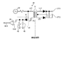
- FIG. 3 is a circuit diagram of a start detection circuit according to the first embodiment.
- FIG. 4 is an operation timing chart of the start detection circuit.
- FIG. 5 is a circuit diagram of a start detection circuit according to a first modification of the first embodiment.
- FIG. 6 is a circuit diagram of a start detection circuit according to a second modification of the first embodiment.
- FIG. 7 is a circuit diagram of a start detection circuit according to the second embodiment.
- FIG. 1 is a schematic block diagram of a storage battery device of the embodiment.
- Storage battery device 10 can be roughly classified into a plurality of (24 in FIG. 1) battery modules 11-1 to 11-24, and a service disk provided between battery module 11-12 and battery module 11-13.
- a connect 12 a current sensor 13, a fuse 14, a BMU (Battery Management Unit) 15, a DC / DC converter 16, a start unit 17, and contactors 18P and 18N are provided.
- BMU Battery Management Unit
- each of the battery modules 11-1 to 11-24 includes a CMU (Cell Monitoring Unit) that monitors the state (temperature, SOC, etc.) of a plurality of cell modules that configure the battery module.
- CMU Cell Monitoring Unit
- a plurality of battery cells are connected in series and parallel to constitute an assembled battery.
- a plurality of cell modules connected in series constitute an assembled battery group.
- each CMU of the battery modules 11-1 to 11-24 performs CAN communication with the BMU 15 and notifies the BMU 15 of the monitoring result.
- BMU 15 notifies the host controller of the end of charge state when it detects the end of charge state in terminal T15A to which the operation start instruction is input from the upper controller not shown and the battery modules 11-1 to 11-24.
- a terminal T15C for notifying the host controller of the near end state a terminal for notifying the host controller of the discharge end state when the end of discharge in the battery modules 11-1 to 11-24 is detected, and the battery module 11- Terminal T1 that notifies the host controller that the high temperature protection state has been reached because 1 to 11-24 become high temperature state It includes a E, a.
- the BMU 15 in order to reduce the power consumption in the standby state, the BMU 15 is stopped in the standby state, and configured to be activated by an activation instruction to the activation unit 17 from the outside.
- FIG. 2 is a schematic block diagram of the startup unit.
- the start unit 17 is in the set state when the start detection circuit 21 for outputting the start detection signal WU1 corresponding to the states of the start terminals 17T1 and 17T2 to the BMU 15 and the start detection signal WU1 at "H" level is input to the set terminal
- An RS flip-flop circuit 24 for causing the power control signal PC1 to transition to the low level to the outside (DC / DC converter 16) to the outside (DC / DC converter 16) in the isolated state via the second photocoupler 23;
- a constant power supply generation circuit 25 for supplying power to the start detection circuit 21 and the RS flip flop circuit 24;
- the base terminal by the dynamic terminal 17T1,17T2 are short-circuited is provided with a transistor 26 for outputting a is the "H" level of the start command WUC grounded, the.
- FIG. 3 is a circuit diagram of a start detection circuit according to a first embodiment.
- the start detection circuit 21 includes an isolation transformer 31 having a high voltage side signal line (primary side winding) LH1 and a low voltage side signal line (secondary side winding) LL1, and a high voltage side signal line LH1 of the isolation transformer 31.
- the oscillator 32 connected to one end of the first detection circuit 33 connected to one end of the high voltage side signal line LH1 of the isolation transformer 31 and the output signal of the first detection circuit 33 are compared with the reference voltage Vref to start up
- a comparator 34 for outputting the detection signal WU1 and a second detection circuit 35 connected between one end of the low voltage side signal line LL1 of the isolation transformer 31 and the start terminal 17T1 are provided.
- the start terminal 17T1 is connected to one end of the low voltage side signal line LL1 of the isolation transformer 31, and the start terminal 17T2 is connected to the ground (frame ground).
- the semiconductor switching element TR is connected between the start terminal 17T1 and the start terminal 17T2.
- the other end of the high voltage side signal line LH1 of the isolation transformer 31 and the first detection circuit 33 are connected to the ground (earth ground), and the other end of the low voltage side signal line LL1 of the isolation transformer 31 is connected to the ground It is done.
- the first detection circuit 33 has an anode terminal connected to the oscillator 32 and one end connected to the diode 41 performing single-wave rectification and a cathode terminal of the diode 41, and the other end connected to ground to smooth the output of the oscillator 32 And a pull-up resistor 43 connected in parallel with the capacitor 42.
- the second detection circuit 35 has an anode terminal connected to one end of the low voltage side signal line LL1 of the isolation transformer 31 and one end connected to a diode 45 performing single-wave rectification and a cathode terminal of the diode 45, and the other end connected to ground. And a capacitor 46 for smoothing the output of the oscillator 32 that is connected and input via the isolation transformer 31.
- FIG. 4 is an operation timing chart of the start detection circuit.
- time t1 is a timing at which the start terminal 17T1 is shorted to the ground via the semiconductor switching element TR connected between the start terminal 17T1 and the start terminal 17T2 and the start terminal 17T2.
- the output waveform of the oscillator 32 is subjected to one-wave rectification, and a smoothed signal is output as the output of the first detection circuit 33.
- a smoothed signal is output as the output of the first detection circuit 33.
- the output of the first detection circuit 33 gradually decreases and falls below the reference voltage Vref of the comparator at time t3. Then, at time t3, the start detection signal WU1 output from the comparator makes a transition from the “H” level to the “L” level, and is output to the DC / DC converter 16. As a result, the DC / DC converter 16 supplies power to the BMU 15, and the BMU 15 starts control of the battery modules 11-1 to 11-24.
- the semiconductor switching element TR is connected between the start terminal 17T1 and the start terminal 17T2 using an isolation transformer which is a passive element to ensure insulation.
- the start terminal 17T1 can be short-circuited to the ground via the start terminal 17T2, and power consumption during standby can be reduced as much as possible, as in the first embodiment. Maintenance work can be reduced and operation can be facilitated by prolonging the time until the battery overdischarges in the stopped state as much as possible.
- FIG. 5 is a circuit diagram of a start detection circuit according to a first modification of the first embodiment.
- the start-up detection circuit 21 of the first modification includes an isolation transformer 31 having a high voltage side signal line (primary side winding) LH1 and a low voltage side signal line (secondary side winding) LL1;
- the oscillator 32 connected to one end of the high voltage side signal line LH1 of the isolation transformer 31, the first detection circuit 33 connected to one end of the high voltage side signal line LH1 of the isolation transformer 31, and the output of the first detection circuit 33
- a comparator 34 which compares the signal with a reference voltage Vref and outputs a start detection signal WU1.
- a mechanical switch may be provided between the start terminal 17T1 and the start terminal 17T2, or a field worker may use both conductors by conductors. Short-circuit between the children 17T1 and 17T2.
- the start terminal 17T1 can be short-circuited to the ground via the start terminal 17T2 by a mechanical switch or conductor, as in the first embodiment, during standby Power consumption as much as possible, and as long as possible until the battery is overdischarged while the device is stopped, maintenance work can be reduced, operation can be facilitated, and the configuration can be simplified. .
- a detection circuit for performing single-wave rectification is used as the second detection circuit 35. This is a case where a detection circuit that performs double-wave rectification is used as the two detection circuit.
- FIG. 6 is a circuit diagram of a start detection circuit according to a second modification of the first embodiment.
- the same parts as those of the first modification of the first embodiment of FIG. 5 are denoted by the same reference numerals.
- the anode terminal is connected to one end of the low voltage side signal line LL1 of the isolation transformer 31, and the diode 45 performing single-wave rectification on the high potential side;
- a capacitor 51 having one end connected to the terminal and the other end connected to the ground via the middle point of the low voltage side signal line LL1 and smoothing the output of the oscillator 32 input via the isolation transformer 31, and an anode A diode 52 having a terminal connected to ground and a cathode terminal connected to the cathode terminal of the diode 45, and a diode 52 connected to one end of the low voltage side signal line LL1 of the isolation transformer 31 to perform single-wave rectification on the low potential side And.
- the diode 45 and the diode 52 cooperate to perform double-wave rectification on the output waveform of the oscillator 32 transmitted to the low voltage side signal line LL1. By doing so, it becomes possible to reduce the influence of noise and operate more stably.
- FIG. 7 is a circuit diagram of a start detection circuit according to a second embodiment.
- Startup detection circuit 60 is connected in series to resistor 62 and oscillator 62 connected to high potential side signal line LH2 via resistor 61, and is a common mode high frequency current for suppressing common mode high frequency current and reducing noise. It is connected to the connection point of the suppression resistor 63, the high potential side insulation capacitors 64-1 and 64-2 connected in series to the common mode high frequency current suppression resistor 63, and the resistor 61 and the common mode high frequency current suppression resistor 63.
- the first detection circuit 65 a comparator 66 that compares the output signal of the first detection circuit 65 with the reference voltage Vref and outputs the start detection signal WU1, and one end is connected to the ground to suppress the common mode high frequency current Low potential side insulation capacitor connected in series with common mode high frequency current suppression resistor 67 and common mode high frequency current suppression resistor 63 to reduce noise 8-1, a low potential side insulating capacitor 68-2 whose one end is connected to the low potential side insulating capacitor 68-1 and whose other end is connected to the ground via the low potential side signal line LL2, and one end is And a second detection circuit 69 connected to the high potential side insulating capacitor 64-2 and having the other end connected to the start terminal 17T1.
- the first detection circuit 65 has the same configuration as the first detection circuit 33 shown in FIG. 5, and the second detection circuit 69 is similar to the second detection circuit 50 shown in FIG. 5 #. It is composed of
- the high potential side insulating capacitor 64-1 and the high potential side insulating capacitor 64-2 are connected in series, and the low potential side insulating capacitor 68-1 and the low potential side insulating capacitor 68-2 are connected.
- the operation of the second embodiment is the same as that of the first modification of the first embodiment, the detailed description thereof is used.
- a capacitor which is a passive element is used to secure the insulation, and when the BMU 15 is activated, the activation terminal 17T1 is grounded via the activation terminal 17T2. It is possible to reduce power consumption during standby, and in the stopped state of BMU 15, insulation can be secured without the need to use an isolated power supply, and power consumption during standby can be reduced as much as possible. The maintenance work can be reduced and the operation can be facilitated by prolonging the time until the battery is overdischarged as long as the device is stopped.
Landscapes
- Physics & Mathematics (AREA)
- General Physics & Mathematics (AREA)
- Engineering & Computer Science (AREA)
- Manufacturing & Machinery (AREA)
- Chemical & Material Sciences (AREA)
- Chemical Kinetics & Catalysis (AREA)
- Electrochemistry (AREA)
- General Chemical & Material Sciences (AREA)
- Secondary Cells (AREA)
- Measurement Of Current Or Voltage (AREA)
Abstract
実施形態の蓄電池装置は、蓄電池モジュールと、蓄電池モジュールを監視する蓄電池監視ユニットと、起動信号により蓄電池監視ユニットの起動制御を行う起動ユニットと、を備え、起動ユニットは、一端がアースに接地された高電圧側信号線及び一端がグランドに接地された低電圧側信号線とを有し、受動素子で構成された絶縁回路と、高電圧側信号線の他端に接続された発振器と、高電圧側信号線の他端に接続され、発振器の出力信号を検波する検波回路と、検波回路の出力信号を所定の基準電圧と比較し、低電圧側信号線の他端に設けられた起動端子がグランドに短絡されて検波回路の出力信号レベルが基準電圧よりも低下したことを検出して起動信号を出力する比較部と、を備えるので、待機時の消費電力を出来る限り低減し、装置停止状態で電池が過放電になるまでの時間を出来る限り長くして、メンテナンス作業を低減し、運用を容易とできる。
Description
本発明の実施形態は、蓄電池装置及び起動検出回路に関する。
従来鉛蓄電池で構成されていた100Vや125V出力の産業機器用直流電源盤をリチウムイオン電池で置き換えることを考えたとき、鉛蓄電池では電池セル毎の監視回路は不要であったがリチウムイオン電池ではそれらが必要である。
一方で、監視回路は電池セルに取り付けられる回路なので電池への充放電電流が流れる主回路と同じ電位を持つが、主回路電圧が高い場合に監視回路の制御入出力は安全面から主回路と絶縁することが望ましい。
そのため、従来は、絶縁電源とフォトカプラで構成される回路が一般的であった。
そのため、従来は、絶縁電源とフォトカプラで構成される回路が一般的であった。
しかしながら、従来技術においては、装置の起動入力については装置が停止状態でも低負荷で(低効率で)絶縁電源を使用しており、装置停止状態で電池が過放電になるまでの時間が短くなってしまうという不具合があった。
本発明は、上記に鑑みてなされたものであって、装置停止状態、すなわち、待機時の消費電力を出来る限り低減し、装置停止状態で電池が過放電になるまでの時間を出来る限り長くして、メンテナンス作業を低減し、運用を容易とすることが可能な蓄電池装置及び起動検出回路を提供することにある。
実施形態の蓄電池装置は、蓄電池モジュールと、蓄電池モジュールを監視する蓄電池監視ユニットと、起動信号により蓄電池監視ユニットの起動制御を行う起動ユニットと、を備え、起動ユニットは、一端がアースに接地された高電圧側信号線及び一端がグランドに接地された低電圧側信号線とを有し、受動素子で構成された絶縁回路と、高電圧側信号線の他端に接続された発振器と、高電圧側信号線の他端に接続され、発振器の出力信号を検波する検波回路と、検波回路の出力信号を所定の基準電圧と比較し、低電圧側信号線の他端に設けられた起動端子がグランドに短絡されて検波回路の出力信号レベルが基準電圧よりも低下したことを検出して起動信号を出力する比較部と、を備える。
次に図面を参照して実施形態の好適な実施形態について説明する。
図1は、実施形態の蓄電池装置の概要構成ブロック図である。
蓄電池装置10は、大別すると、複数(図1では、24個)のバッテリモジュール11-1~11-24と、バッテリモジュール11-12とバッテリモジュール11-13との間に設けられたサービスディスコネクト12と、電流センサ13と、ヒューズ14と、BMU(Battery Management Unit)15と、DC/DCコンバータ16と、起動ユニット17と、コンタクタ18P、18Nと、を備えている。
図1は、実施形態の蓄電池装置の概要構成ブロック図である。
蓄電池装置10は、大別すると、複数(図1では、24個)のバッテリモジュール11-1~11-24と、バッテリモジュール11-12とバッテリモジュール11-13との間に設けられたサービスディスコネクト12と、電流センサ13と、ヒューズ14と、BMU(Battery Management Unit)15と、DC/DCコンバータ16と、起動ユニット17と、コンタクタ18P、18Nと、を備えている。
上記構成において、バッテリモジュール11-1~11-24は、それぞれ当該バッテリモジュールを構成する複数のセルモジュールの状態(温度、SOC等)の監視を行うCMU(Cell Monitoring Unit)を備えている。
ここで、各バッテリモジュール11-1~11-24を構成しているセルモジュールは、電池セルが複数、直並列に接続されて組電池を構成している。そして、複数の直列接続されたセルモジュールで組電池群を構成している。
また、バッテリモジュール11-1~11-24の各CMUは、BMU15との間でCAN通信を行って監視結果をBMU15に通知している。
また、BMU15は,図示しない上位制御装置から運転開始指示が入力される端子T15Aと、バッテリモジュール11-1~11-24における充電末状態を検出した場合に充電末状態を上位制御装置に通知する端子T15B、バッテリモジュール11-1~11-24における放電末近傍状態(未だ放電末には至っていないが、そのまま放電を継続すると放電末に容易に至る可能性のある状態)を検出した場合に放電末近傍状態を上位制御装置に通知する端子T15Cと、バッテリモジュール11-1~11-24における放電末状態を検出した場合に放電末状態を上位制御装置に通知する端子T15Dと、バッテリモジュール11-1~11-24が高温度状態となり、高温度保護状態に至ったことを上位制御装置に通知する端子T15Eと、を備えている。
また、BMU15は,図示しない上位制御装置から運転開始指示が入力される端子T15Aと、バッテリモジュール11-1~11-24における充電末状態を検出した場合に充電末状態を上位制御装置に通知する端子T15B、バッテリモジュール11-1~11-24における放電末近傍状態(未だ放電末には至っていないが、そのまま放電を継続すると放電末に容易に至る可能性のある状態)を検出した場合に放電末近傍状態を上位制御装置に通知する端子T15Cと、バッテリモジュール11-1~11-24における放電末状態を検出した場合に放電末状態を上位制御装置に通知する端子T15Dと、バッテリモジュール11-1~11-24が高温度状態となり、高温度保護状態に至ったことを上位制御装置に通知する端子T15Eと、を備えている。
本実施形態の蓄電池装置においては、待機状態における消費電力を低減するために、待機状態において、BMU15を停止状態として、外部からの起動ユニットに17に対する起動指示により起動するように構成している。
図2は、起動ユニットの概要構成ブロック図である。
起動ユニット17は、起動端子17T1、17T2の状態に対応する起動検出信号WU1をBMU15に出力する起動検出回路21と、“H”レベルの起動検出信号WU1がセット端子に入力されるとセット状態となり、自立遮断信号SD0が第1フォトカプラ22を介して“L”レベルの自立遮断信号SD1(=リセット信号)となることによりによりリセット状態となり、電源制御信号PC0を“H”レベルとすることにより第2フォトカプラ23を介して絶縁状態で外部(DC/DCコンバータ16)に対する電源制御信号PC1を“L”レベルに遷移させるRSフリップフロップ回路24と、主回路から電力信号SPの供給がなされ、起動検出回路21及びRSフリップフロップ回路24に電源を供給する常時電源生成回路25と、起動端子17T1、17T2が短絡されることによりベース端子がグランドに接地されると“H”レベルの起動指令WUCを出力するトランジスタ26と、を備えている。
起動ユニット17は、起動端子17T1、17T2の状態に対応する起動検出信号WU1をBMU15に出力する起動検出回路21と、“H”レベルの起動検出信号WU1がセット端子に入力されるとセット状態となり、自立遮断信号SD0が第1フォトカプラ22を介して“L”レベルの自立遮断信号SD1(=リセット信号)となることによりによりリセット状態となり、電源制御信号PC0を“H”レベルとすることにより第2フォトカプラ23を介して絶縁状態で外部(DC/DCコンバータ16)に対する電源制御信号PC1を“L”レベルに遷移させるRSフリップフロップ回路24と、主回路から電力信号SPの供給がなされ、起動検出回路21及びRSフリップフロップ回路24に電源を供給する常時電源生成回路25と、起動端子17T1、17T2が短絡されることによりベース端子がグランドに接地されると“H”レベルの起動指令WUCを出力するトランジスタ26と、を備えている。
[1]第1実施形態
図3は、第1実施形態の起動検出回路の回路構成図である。
起動検出回路21は、高電圧側信号線(一次側巻線)LH1と低電圧側信号線(二次側巻線)LL1とを有する絶縁トランス31と、絶縁トランス31の高電圧側信号線LH1の一端に接続された発振器32と、絶縁トランス31の高電圧側信号線LH1の一端に接続された第1検波回路33と、第1検波回路33の出力信号を基準電圧Vrefと比較して起動検出信号WU1を出力する比較器34と、絶縁トランス31の低電圧側信号線LL1の一端及び起動端子17T1との間に接続された第2検波回路35と、を備えている。
図3は、第1実施形態の起動検出回路の回路構成図である。
起動検出回路21は、高電圧側信号線(一次側巻線)LH1と低電圧側信号線(二次側巻線)LL1とを有する絶縁トランス31と、絶縁トランス31の高電圧側信号線LH1の一端に接続された発振器32と、絶縁トランス31の高電圧側信号線LH1の一端に接続された第1検波回路33と、第1検波回路33の出力信号を基準電圧Vrefと比較して起動検出信号WU1を出力する比較器34と、絶縁トランス31の低電圧側信号線LL1の一端及び起動端子17T1との間に接続された第2検波回路35と、を備えている。
上記構成において、絶縁トランス31の低電圧側信号線LL1の一端に起動端子17T1が接続され、起動端子17T2がグランド(フレームグランド)に接続されている。
この場合において、起動端子17T1と、起動端子17T2との間には、半導体スイッチング素子TRが接続される。
この場合において、起動端子17T1と、起動端子17T2との間には、半導体スイッチング素子TRが接続される。
また、絶縁トランス31の高電圧側信号線LH1の他端及び第1検波回路33は、アース(大地接地)に接続され、絶縁トランス31の低電圧側信号線LL1の他端は、グランドに接続されている。
第1検波回路33は、アノード端子が発振器32に接続され片波整流を行うダイオード41と、ダイオード41のカソード端子に一端が接続され、他端がアースに接続されて発振器32の出力の平滑化を行うコンデンサ42と、コンデンサ42と並列に接続されたプルアップ抵抗43と、を備えている。
第2検波回路35は、アノード端子が絶縁トランス31の低電圧側信号線LL1の一端に接続され片波整流を行うダイオード45と、ダイオード45のカソード端子に一端が接続され、他端がグランドに接続されて絶縁トランス31を介して入力される発振器32の出力の平滑化を行うコンデンサ46と、を備えている。
次に起動検出回路21の動作について説明する。
図4は、起動検出回路の動作タイミングチャートである。
図4において、時刻t1は、起動端子17T1を、起動端子17T1と起動端子17T2との間に接続した半導体スイッチング素子TR及び起動端子17T2を介してグランドとを短絡したタイミングである。
図4は、起動検出回路の動作タイミングチャートである。
図4において、時刻t1は、起動端子17T1を、起動端子17T1と起動端子17T2との間に接続した半導体スイッチング素子TR及び起動端子17T2を介してグランドとを短絡したタイミングである。
時刻t1より前の期間においては、図4(A)の示すように発振器32の出力として、所定周波数のパルス信号を出力した場合、起動端子17T1においては、図4(B)に示すように、発振器32の出力波形が絶縁トランス31により変圧された電圧波形が出力されているのを検出することができる。
一方、第1検波回路33の出力には図4(C)に示すように、発振器32の出力波形を片波整流し、平滑化した信号が出力される。
そして、時刻t1に至り、起動端子17T1を、起動端子17T1と起動端子17T2との間に接続した半導体スイッチング素子TR及び起動端子17T2を介してグランドに短絡させると、図4(B)に示すように、起動端子17T1-起動端子17T2間の出力電圧は低下し、最終的には時刻t2において、グランドの電圧レベルとなる。
そして、時刻t1に至り、起動端子17T1を、起動端子17T1と起動端子17T2との間に接続した半導体スイッチング素子TR及び起動端子17T2を介してグランドに短絡させると、図4(B)に示すように、起動端子17T1-起動端子17T2間の出力電圧は低下し、最終的には時刻t2において、グランドの電圧レベルとなる。
これと並行して、第1検波回路33の出力は、徐々に低下し、時刻t3において比較器の基準電圧Vrefを下回ることとなる。
そして、時刻t3において、比較器から出力される起動検出信号WU1は、“H”レベルから“L”レベルに遷移し、DC/DCコンバータ16に出力される。
これらの結果、DC/DCコンバータ16は、BMU15に電源を供給し、BMU15は、各バッテリモジュール11-1~11-24の制御を開始することとなる。
そして、時刻t3において、比較器から出力される起動検出信号WU1は、“H”レベルから“L”レベルに遷移し、DC/DCコンバータ16に出力される。
これらの結果、DC/DCコンバータ16は、BMU15に電源を供給し、BMU15は、各バッテリモジュール11-1~11-24の制御を開始することとなる。
以上の説明のように、本第1実施形態によれば、絶縁を確保するのに受動素子である絶縁トランスを用い、さらに起動端子17T1と起動端子17T2との間に半導体スイッチング素子TRを接続し、当該半導体スイッチング素子TRを制御することで、起動端子17T1を起動端子17T2を介してグランドに短絡させることができ、第1実施形態と同様に、待機時の消費電力を出来る限り低減し、装置停止状態で電池が過放電になるまでの時間を出来る限り長くして、メンテナンス作業を低減し、運用を容易とすることができる。
[1.1]第1実施形態の第1変形例
上記第1実施形態においては、起動端子17T1と起動端子17T2との間を半導体スイッチング素子TRにより短絡することにより起動制御を行う場合について説明したが、本第1変形例は、起動端子17T1と起動端子17T2とを機械的スイッチあるいは導体により短絡するためのものである。
上記第1実施形態においては、起動端子17T1と起動端子17T2との間を半導体スイッチング素子TRにより短絡することにより起動制御を行う場合について説明したが、本第1変形例は、起動端子17T1と起動端子17T2とを機械的スイッチあるいは導体により短絡するためのものである。
図5は、第1実施形態の第1変形例の起動検出回路の回路構成図である。
図3の第1実施形態と異なる点は、第2検波回路35を省略した点である。
具体的には、第1変形例の起動検出回路21は、高電圧側信号線(一次側巻線)LH1と低電圧側信号線(二次側巻線)LL1とを有する絶縁トランス31と、絶縁トランス31の高電圧側信号線LH1の一端に接続された発振器32と、絶縁トランス31の高電圧側信号線LH1の一端に接続された第1検波回路33と、第1検波回路33の出力信号を基準電圧Vrefと比較して起動検出信号WU1を出力する比較器34と、を備えている。
図3の第1実施形態と異なる点は、第2検波回路35を省略した点である。
具体的には、第1変形例の起動検出回路21は、高電圧側信号線(一次側巻線)LH1と低電圧側信号線(二次側巻線)LL1とを有する絶縁トランス31と、絶縁トランス31の高電圧側信号線LH1の一端に接続された発振器32と、絶縁トランス31の高電圧側信号線LH1の一端に接続された第1検波回路33と、第1検波回路33の出力信号を基準電圧Vrefと比較して起動検出信号WU1を出力する比較器34と、を備えている。
この場合において、起動端子17T1と起動端子17T2とを短絡する方法としては、起動端子17T1と起動端子17T2との間に機械的スイッチ(リレー等)を設けるか、あるいは、現地作業員が導体により両端子17T1、17T2間を短絡させる。
本第1実施形態の第1変形例の構成によれば、機械的スイッチあるいは導体により起動端子17T1を起動端子17T2を介してグランドに短絡させることができ、第1実施形態と同様に、待機時の消費電力を出来る限り低減し、装置停止状態で電池が過放電になるまでの時間を出来る限り長くして、メンテナンス作業を低減し、運用を容易とすることができるとともに、構成を簡略化できる。
[1.2]第1実施形態の第2変形例
上記第1実施形態においては、第2検波回路35として、片波整流を行う検波回路を用いていたが、本第2変形例は、第2検波回路として、両波整流を行う検波回路を用いた場合のものである。
上記第1実施形態においては、第2検波回路35として、片波整流を行う検波回路を用いていたが、本第2変形例は、第2検波回路として、両波整流を行う検波回路を用いた場合のものである。
図6は、第1実施形態の第2変形例の起動検出回路の回路構成図である。
図6において、図5の第1実施形態の第1変形例と同様の部分には、同一の符号を付すものとする。
図6において、図5の第1実施形態の第1変形例と同様の部分には、同一の符号を付すものとする。
第2の検波回路50は、図6に示すように、アノード端子が絶縁トランス31の低電圧側信号線LL1の一端に接続され高電位側の片波整流を行うダイオード45と、ダイオード45のカソード端子に一端が接続され、他端が低電圧側信号線LL1の中点を介してグランドに接続され、絶縁トランス31を介して入力される発振器32の出力の平滑化を行うコンデンサ51と、アノード端子がグランドに接続され、カソード端子がダイオード45のカソード端子に接続されたダイオード52と、絶縁トランス31の低電圧側信号線LL1の一端に接続され低電位側の片波整流を行うダイオード52と、を備えている。
すなわち、本第1実施形態の第2変形例の構成によれば、ダイオード45及びダイオード52は、共働して低電圧側の信号線LL1に伝送される発振器32の出力波形を両波整流を行うので、ノイズの影響を低減してより安定して動作することが可能となる。
[2]第2実施形態
図7は、第2実施形態の起動検出回路の回路構成図である。
起動検出回路60は、高電位側信号線LH2に抵抗61を介して接続された発振器62と、抵抗61に直列接続され、コモンモード高周波電流を抑制してノイズを低減するためのコモンモード高周波電流抑制抵抗63と、コモンモード高周波電流抑制抵抗63に直列接続された高電位側絶縁用コンデンサ64-1、64-2と、抵抗61とコモンモード高周波電流抑制抵抗63との接続点に接続された第1検波回路65と、第1検波回路65の出力信号を基準電圧Vrefと比較して起動検出信号WU1を出力する比較器66と、一端がアースに接続され、コモンモード高周波電流を抑制してノイズを低減するためのコモンモード高周波電流抑制抵抗67と、コモンモード高周波電流抑制抵抗63に直列接続された低電位側絶縁用コンデンサ68-1と、一端が低電位側絶縁用コンデンサ68-1に接続され、他端が低電位側信号線LL2を介してグランドに接続された低電位側絶縁用コンデンサ68-2と、一端が高電位側絶縁用コンデンサ64-2に接続され、他端が起動端子17T1に接続された第2検波回路69と、を備えている。
図7は、第2実施形態の起動検出回路の回路構成図である。
起動検出回路60は、高電位側信号線LH2に抵抗61を介して接続された発振器62と、抵抗61に直列接続され、コモンモード高周波電流を抑制してノイズを低減するためのコモンモード高周波電流抑制抵抗63と、コモンモード高周波電流抑制抵抗63に直列接続された高電位側絶縁用コンデンサ64-1、64-2と、抵抗61とコモンモード高周波電流抑制抵抗63との接続点に接続された第1検波回路65と、第1検波回路65の出力信号を基準電圧Vrefと比較して起動検出信号WU1を出力する比較器66と、一端がアースに接続され、コモンモード高周波電流を抑制してノイズを低減するためのコモンモード高周波電流抑制抵抗67と、コモンモード高周波電流抑制抵抗63に直列接続された低電位側絶縁用コンデンサ68-1と、一端が低電位側絶縁用コンデンサ68-1に接続され、他端が低電位側信号線LL2を介してグランドに接続された低電位側絶縁用コンデンサ68-2と、一端が高電位側絶縁用コンデンサ64-2に接続され、他端が起動端子17T1に接続された第2検波回路69と、を備えている。
上記構成において、第1検波回路65は、図5に示した第1検波回路33と同様の構成を有し、第2検波回路69は、図5#に示した第2の検波回路50と同様の構成をしている。
また、上記構成において、高電位側絶縁用コンデンサ64-1と高電位側絶縁用コンデンサ64-2とを直列接続し、低電位側絶縁用コンデンサ68-1と低電位側絶縁用コンデンサ68-2とを直列接続しているのは、いずれかのコンデンサが短絡モード故障を起こした場合に漏電を防止するためであり、二個直列接続する構成に限られず、3個以上直列接続する構成を採ることも可能である。なお、原理的には、一つのコンデンサで絶縁を確保することが可能である。
本第2実施形態の動作は第1実施形態の第1変形例と同様であるので、その詳細な説明を援用するものとする。
本第2実施形態によっても、第1実施形態と同様に、絶縁を確保するのに、受動素子であるコンデンサを用い、BMU15を起動させる際には、起動端子17T1を起動端子17T2を介してグランドに短絡させるだけであるため、待機時における消費電力の低減を図ることができ、BMU15の停止状態においては、絶縁電源を使用する必要なしに絶縁を確保でき、待機時の消費電力を出来る限り低減し、装置停止状態で電池が過放電になるまでの時間を出来る限り長くして、メンテナンス作業を低減し、運用を容易とすることができる。
本第2実施形態によっても、第1実施形態と同様に、絶縁を確保するのに、受動素子であるコンデンサを用い、BMU15を起動させる際には、起動端子17T1を起動端子17T2を介してグランドに短絡させるだけであるため、待機時における消費電力の低減を図ることができ、BMU15の停止状態においては、絶縁電源を使用する必要なしに絶縁を確保でき、待機時の消費電力を出来る限り低減し、装置停止状態で電池が過放電になるまでの時間を出来る限り長くして、メンテナンス作業を低減し、運用を容易とすることができる。
本発明のいくつかの実施形態を説明したが、これらの実施形態は、例として提示したものであり、発明の範囲を限定することは意図していない。これら新規な実施形態は、その他の様々な形態で実施されることが可能であり、発明の要旨を逸脱しない範囲で、種々の省略、置き換え、変更を行うことができる。これら実施形態やその変形は、発明の範囲や要旨に含まれるとともに、請求の範囲に記載された発明とその均等の範囲に含まれる。
Claims (5)
- 蓄電池モジュールと、
前記蓄電池モジュールを監視する蓄電池監視ユニットと、
起動信号により前記蓄電池監視ユニットの起動制御を行う起動ユニットと、を備え、
前記起動ユニットは、
一端がアースに接地された高電圧側信号線及び一端がグランドに接地された低電圧側信号線とを有し、受動素子で構成された絶縁回路と、
前記高電圧側信号線の他端に接続された発振器と、
前記高電圧側信号線の他端に接続され、前記発振器の出力信号を検波する検波回路と、
前記検波回路の出力信号を所定の基準電圧と比較し、前記低電圧側信号線の他端に設けられた起動端子が前記グランドに短絡されて前記検波回路の出力信号レベルが前記基準電圧よりも低下したことを検出して前記起動信号を出力する比較部と、
を備えた蓄電池装置。 - 前記低電圧側信号線の他端に接続され、前記絶縁回路を介した前記発振器の出力信号を検波する第2の検波回路を備えた、
請求項1記載の蓄電池装置。 - 前記絶縁回路は、一方の巻線が前記高電圧側信号線とされ、他方の巻線が前記低電圧側信号線とされた絶縁トランスとして構成されている、
請求項1又は請求項2記載の蓄電池装置。 - 前記絶縁回路は、複数のコンデンサが直列接続された一対のコンデンサ群のうち一方が前記高電圧側信号線と前記低電圧側信号線との間で接続され、他方が前記アースと前記グランドとの間で接続されている、
請求項1または請求項2記載の蓄電池装置。 - 蓄電池からの電力供給を受けて駆動される起動対象装置を起動させるための起動信号を出力する起動検出回路であって、
一端がアースに接地された高電圧側信号線及び一端がグランドに接地された低電圧側信号線とを有し、受動素子で構成された絶縁回路と、
前記蓄電池からの電力を供給を受けて動作するとともに、前記高電圧側信号線の他端に接続された発振器と、
前記高電圧側信号線の他端に接続され、前記発振器の出力信号を検波する検波回路と、
前記検波回路の出力信号を所定の基準電圧と比較し、前記低電圧側信号線の他端に設けられた起動端子が前記グランドに短絡されて前記検波回路の出力信号レベルが前記基準電圧よりも低下したことを検出して前記起動信号を出力する比較部と、
を備えた起動検出回路。
Priority Applications (2)
| Application Number | Priority Date | Filing Date | Title |
|---|---|---|---|
| PCT/JP2017/037248 WO2019073608A1 (ja) | 2017-10-13 | 2017-10-13 | 蓄電池装置及び起動検出回路 |
| JP2019547891A JP6866496B2 (ja) | 2017-10-13 | 2017-10-13 | 蓄電池装置及び起動検出回路 |
Applications Claiming Priority (1)
| Application Number | Priority Date | Filing Date | Title |
|---|---|---|---|
| PCT/JP2017/037248 WO2019073608A1 (ja) | 2017-10-13 | 2017-10-13 | 蓄電池装置及び起動検出回路 |
Publications (1)
| Publication Number | Publication Date |
|---|---|
| WO2019073608A1 true WO2019073608A1 (ja) | 2019-04-18 |
Family
ID=66100548
Family Applications (1)
| Application Number | Title | Priority Date | Filing Date |
|---|---|---|---|
| PCT/JP2017/037248 Ceased WO2019073608A1 (ja) | 2017-10-13 | 2017-10-13 | 蓄電池装置及び起動検出回路 |
Country Status (2)
| Country | Link |
|---|---|
| JP (1) | JP6866496B2 (ja) |
| WO (1) | WO2019073608A1 (ja) |
Families Citing this family (1)
| Publication number | Priority date | Publication date | Assignee | Title |
|---|---|---|---|---|
| CN111122957B (zh) * | 2019-12-26 | 2022-08-09 | 上海三菱电机·上菱空调机电器有限公司 | 过电压检测电路、过电压检测方法、逆变器及空气调节器 |
Citations (4)
| Publication number | Priority date | Publication date | Assignee | Title |
|---|---|---|---|---|
| JPS63263822A (ja) * | 1987-04-21 | 1988-10-31 | Hoxan Corp | タツチスイツチ装置 |
| JP2011166867A (ja) * | 2010-02-05 | 2011-08-25 | Hitachi Vehicle Energy Ltd | 電池制御装置および電池システム |
| JP2013024675A (ja) * | 2011-07-20 | 2013-02-04 | Denso Corp | 電池監視装置 |
| JP2014168177A (ja) * | 2013-02-28 | 2014-09-11 | Brother Ind Ltd | 通信装置 |
-
2017
- 2017-10-13 JP JP2019547891A patent/JP6866496B2/ja active Active
- 2017-10-13 WO PCT/JP2017/037248 patent/WO2019073608A1/ja not_active Ceased
Patent Citations (4)
| Publication number | Priority date | Publication date | Assignee | Title |
|---|---|---|---|---|
| JPS63263822A (ja) * | 1987-04-21 | 1988-10-31 | Hoxan Corp | タツチスイツチ装置 |
| JP2011166867A (ja) * | 2010-02-05 | 2011-08-25 | Hitachi Vehicle Energy Ltd | 電池制御装置および電池システム |
| JP2013024675A (ja) * | 2011-07-20 | 2013-02-04 | Denso Corp | 電池監視装置 |
| JP2014168177A (ja) * | 2013-02-28 | 2014-09-11 | Brother Ind Ltd | 通信装置 |
Also Published As
| Publication number | Publication date |
|---|---|
| JPWO2019073608A1 (ja) | 2020-07-27 |
| JP6866496B2 (ja) | 2021-04-28 |
Similar Documents
| Publication | Publication Date | Title |
|---|---|---|
| US10404095B2 (en) | Uninterruptible power supply unit | |
| JP5484597B2 (ja) | 逆接続保護装置及びこれを備えるバックアップ電源 | |
| CN102742140B (zh) | 带有多馈机载供电装置的功率逆变器 | |
| US9461484B2 (en) | Electricity storage system, method for controlling secondary battery packs, and secondary battery pack | |
| CN103733381A (zh) | 保护电池组的元件 | |
| US20190288504A1 (en) | Double fusing of the module store interface | |
| JPWO2014129126A1 (ja) | スイッチング電源装置 | |
| CN103999361B (zh) | 高输出功率放大器 | |
| CN113972817B (zh) | 固态变压器故障处理系统 | |
| US20110057626A1 (en) | Power supply and charging circuit for high energy capacitors | |
| US11909237B2 (en) | Reverse polarity protected battery module | |
| US11955836B2 (en) | Power device terminal backup switch unit | |
| JP2008193757A (ja) | 車両用の電源装置 | |
| CN116094011A (zh) | 储能系统 | |
| JP2016524439A (ja) | 無停電直流電源装置 | |
| CN105391112B (zh) | 一种通信用移动应急电源及其电压自适应方法 | |
| CN104426127B (zh) | 一种负载启动电路 | |
| JP2015042084A (ja) | 組電池モジュール | |
| KR20180099279A (ko) | 에너지 저장 장치를 포함하는 에너지 저장 시스템 | |
| JP5828774B2 (ja) | 2次電池の充放電装置およびそれを用いた充放電検査装置 | |
| JP6866496B2 (ja) | 蓄電池装置及び起動検出回路 | |
| US10305128B2 (en) | Cell system and control method for cell system | |
| EP3091634A1 (en) | Power supply device for hvdc controller | |
| JP6707373B2 (ja) | セルバランス装置 | |
| KR101837548B1 (ko) | 커패시터 관리 시스템 |
Legal Events
| Date | Code | Title | Description |
|---|---|---|---|
| 121 | Ep: the epo has been informed by wipo that ep was designated in this application |
Ref document number: 17928685 Country of ref document: EP Kind code of ref document: A1 |
|
| ENP | Entry into the national phase |
Ref document number: 2019547891 Country of ref document: JP Kind code of ref document: A |
|
| NENP | Non-entry into the national phase |
Ref country code: DE |
|
| 122 | Ep: pct application non-entry in european phase |
Ref document number: 17928685 Country of ref document: EP Kind code of ref document: A1 |