WO2019059102A1 - 炭化珪素半導体基板を用いた半導体装置の製造方法 - Google Patents
炭化珪素半導体基板を用いた半導体装置の製造方法 Download PDFInfo
- Publication number
- WO2019059102A1 WO2019059102A1 PCT/JP2018/034054 JP2018034054W WO2019059102A1 WO 2019059102 A1 WO2019059102 A1 WO 2019059102A1 JP 2018034054 W JP2018034054 W JP 2018034054W WO 2019059102 A1 WO2019059102 A1 WO 2019059102A1
- Authority
- WO
- WIPO (PCT)
- Prior art keywords
- trench
- epitaxial layer
- silicon carbide
- shape
- forming
- Prior art date
- Legal status (The legal status is an assumption and is not a legal conclusion. Google has not performed a legal analysis and makes no representation as to the accuracy of the status listed.)
- Ceased
Links
Images






Classifications
-
- G—PHYSICS
- G03—PHOTOGRAPHY; CINEMATOGRAPHY; ANALOGOUS TECHNIQUES USING WAVES OTHER THAN OPTICAL WAVES; ELECTROGRAPHY; HOLOGRAPHY
- G03F—PHOTOMECHANICAL PRODUCTION OF TEXTURED OR PATTERNED SURFACES, e.g. FOR PRINTING, FOR PROCESSING OF SEMICONDUCTOR DEVICES; MATERIALS THEREFOR; ORIGINALS THEREFOR; APPARATUS SPECIALLY ADAPTED THEREFOR
- G03F9/00—Registration or positioning of originals, masks, frames, photographic sheets or textured or patterned surfaces, e.g. automatically
-
- H—ELECTRICITY
- H10—SEMICONDUCTOR DEVICES; ELECTRIC SOLID-STATE DEVICES NOT OTHERWISE PROVIDED FOR
- H10P—GENERIC PROCESSES OR APPARATUS FOR THE MANUFACTURE OR TREATMENT OF DEVICES COVERED BY CLASS H10
- H10P14/00—Formation of materials, e.g. in the shape of layers or pillars
- H10P14/20—Formation of materials, e.g. in the shape of layers or pillars of semiconductor materials
-
- H—ELECTRICITY
- H10—SEMICONDUCTOR DEVICES; ELECTRIC SOLID-STATE DEVICES NOT OTHERWISE PROVIDED FOR
- H10P—GENERIC PROCESSES OR APPARATUS FOR THE MANUFACTURE OR TREATMENT OF DEVICES COVERED BY CLASS H10
- H10P72/00—Handling or holding of wafers, substrates or devices during manufacture or treatment thereof
- H10P72/50—Handling or holding of wafers, substrates or devices during manufacture or treatment thereof for positioning, orientation or alignment
Definitions
- the present disclosure relates to a method of manufacturing a SiC semiconductor device configured using a silicon carbide (hereinafter referred to as SiC) semiconductor substrate on which alignment marks are formed.
- SiC silicon carbide
- a trench serving as an alignment mark is formed on such a SiC semiconductor substrate, and an impurity region having a planar pattern is formed by ion implantation or the like.
- a predetermined manufacturing process such as growing an epitaxial layer or heat treatment is performed.
- the position of the alignment mark is specified by the reader, and a predetermined semiconductor manufacturing process using resist patterning or the like is subsequently performed based on the alignment mark.
- the epitaxial layer when the epitaxial layer is grown on the SiC semiconductor substrate in which the trench is formed, the epitaxial layer may not grow (that is, deposit) along the wall surface on the downstream side in the off direction of the trench. . That is, when the epitaxial layer is grown on the SiC semiconductor substrate, the epitaxial layer may be grown on the downstream side in the off direction of the trench so as to form a facet of the (0001) plane. In this case, the position of the alignment mark can not be specified with high precision due to the influence of the facets, and pattern deviation may occur before and after formation of the epitaxial layer.
- Patent Document 1 when an epitaxial layer is grown on a SiC semiconductor substrate and a facet is formed on the downstream side in the off direction of the trench, a new trench is formed on the facet. It has been disclosed to form
- the new trench is formed in the facet of the (0001) plane. Therefore, even if the epitaxial layer is further grown on the SiC semiconductor substrate or heat treatment is performed, formation of a facet on the downstream side in the off direction of the new trench can be suppressed. it can. Therefore, by reading the new trench as the alignment mark by the reader, it is possible to suppress the occurrence of positional deviation when specifying the position of the alignment mark.
- the off direction means "a direction parallel to a vector obtained by projecting the normal vector of the growth surface onto the (0001) plane".
- the downstream side in the off direction defines one of the sides, and means "the side where the tip of the vector obtained by projecting the normal vector of the growth surface onto the (0001) plane is facing”.
- An object of the present disclosure is to provide a method of manufacturing a SiC semiconductor device capable of accurately reading a trench formed in an epitaxial layer without increasing or complicating a manufacturing process.
- a SiC semiconductor device in a method of manufacturing a SiC semiconductor device, it is a SiC single crystal having a main surface provided with an off angle in the (0001) plane and having an off direction of ⁇ 11-20>.
- Providing a structured SiC semiconductor substrate, forming a first trench in the main surface, and SiC having a second trench on the main surface that inherits the shape of the first trench formed in the main surface And growing the epitaxial layer formed in the second trench and performing predetermined processing by reading the second trench, and forming the first trench, the opening is rectangular and the longitudinal direction is off.
- a plurality of first trenches parallel to the direction are formed along the direction orthogonal to the off direction.
- the openings are rectangular and a plurality of first trenches having a longitudinal direction parallel to the off direction are formed along the direction orthogonal to the off direction, the first trenches are turned off.
- the length in the direction orthogonal to the direction becomes short. Therefore, when the epitaxial layer is grown, formation of facets can be suppressed on the downstream side in the off direction of each first trench. Therefore, the second trench can be read with high accuracy.
- the manufacturing process is not increased or complicated.
- FIG. 7 is a cross-sectional view showing the manufacturing process of the SiC semiconductor device in the first embodiment. It is sectional drawing which shows the manufacturing process of the SiC semiconductor device in 1st Embodiment following FIG. 1A. It is sectional drawing which shows the manufacturing process of the SiC semiconductor device in 1st Embodiment following FIG. 1B. It is a top view which shows the planar shape and arrangement
- FIG. 16 is a cross sectional view showing a manufacturing step of the SiC semiconductor device in the second embodiment, and a cross sectional view of an alignment mark formation region. It is sectional drawing which shows the manufacturing process of the SiC semiconductor device in 2nd Embodiment following FIG. 5A. It is sectional drawing which shows the manufacturing process of the SiC semiconductor device in 2nd Embodiment following FIG. 5B. It is sectional drawing which shows the manufacturing process of the SiC semiconductor device in 2nd Embodiment following FIG. 5C. It is a top view which shows the planar shape and arrangement of a trench used as a mark for alignment inspection. It is a top view of the test pattern vicinity in FIG. 5D.
- the SiC semiconductor substrate 10 configured by the above is prepared.
- a region for forming an alignment mark is referred to as an alignment mark formation region R1
- a region for forming a device such as a semiconductor element is referred to as a device formation region R2.
- a mask material 11 such as a resist is disposed on the main surface of SiC semiconductor substrate 10, and a region corresponding to a trench formation planned region of mask material 11 is opened. Then, while the SiC semiconductor substrate 10 is covered with the mask material 11, anisotropic dry etching such as RIE (that is, Reactive Ion Etching) is performed to form a trench 12 to be an alignment mark in the alignment mark formation region R1. Do. In the present embodiment, the trench 12 corresponds to a first trench and a first main trench.
- RIE Reactive Ion Etching
- a plurality of trenches 12 having rectangular openings and whose longitudinal direction is parallel to the off direction are formed along the direction orthogonal to the off direction.
- the more detailed shape of the trench 12 will be described later.
- an epitaxial layer 13 composed of SiC is grown on the SiC semiconductor substrate 10 by, for example, a CVD (that is, Chemical Vapor Deposition) method.
- a CVD that is, Chemical Vapor Deposition
- the shape of the SiC semiconductor substrate 10 to be the base is taken over to the surface of the epitaxial layer 13. Therefore, on the surface of epitaxial layer 13, trench 14 is formed at a position corresponding to trench 12. Then, the trench 14 becomes a new alignment mark.
- the trench 14 corresponds to a second trench and a second main trench.
- a facet may be formed on the downstream side of the trench 14 in the off direction, but the facet is formed depending on the length of the trench 14 in the direction orthogonal to the off direction. That is, as the length in the direction orthogonal to the off direction is shorter, the facets are less likely to be formed. Therefore, formation of the facets can be suppressed by forming the trench 12 so that the opening has a rectangular shape and the longitudinal direction is parallel to the off direction as in the present embodiment.
- the epitaxial layer 13 if the growth rate is too fast, defects such as 3C-SiC defects may be generated. For this reason, in the present embodiment, the epitaxial layer 13 is grown under the conditions of a growth rate of 2 ⁇ m / h or less.
- the trench 14 serving as an alignment mark is read by a reader (not shown), and a predetermined manufacturing process such as ion implantation or etching is performed on the device formation region R2.
- the laser diode when reading an alignment mark with a reader, the laser diode is irradiated with a plurality of laser beams while scanning the reader, and the SiC semiconductor substrate 10 on which the epitaxial layer 13 is formed is reflected. Analyze the information contained in the received laser light. Thereby, the formation position of the trench 14 is specified.
- the intensity of the laser beam reflected by the epitaxial layer 13 depends on the distance between the light source and the epitaxial layer 13 in the reader, and is compared with the portion where the alignment mark is not formed. Distance becomes longer and the strength becomes weaker. Therefore, the position of the alignment mark can be specified by reading the intensity signals of the plurality of reflected laser beams, for example.
- the reading device converts the read intensity signal into a signal that causes a peak to appear when the intensity signal changes, for example.
- the position of the alignment mark can also be identified based on the signal.
- the trench 12 has a rectangular shape whose short side is a direction in which the opening is orthogonal to the off direction.
- the formation of facets in the trench 14 is suppressed. Therefore, the reading of the alignment mark by the reader can be performed with high accuracy.
- each trench 12 of the present embodiment will be described with reference to FIGS. 3 and 4.
- the readable range is different between the case where the epitaxial layer 13 is grown to 1.4 ⁇ m and the case where the epitaxial layer 13 is grown to 2.1 ⁇ m, and the film of the epitaxial layer 13 is different.
- the thicker the thickness the narrower the readable range.
- hatched portions that is, portions surrounded by straight lines L1 to L5 each have a shape of trench 12 in which trench 14 can be read with high accuracy.
- the shape of the trench 12 be defined in consideration of the film thickness of the epitaxial layer 13 to be grown, and the trench 12 is formed so as to satisfy all of the following mathematical expressions 1 to 5.
- the length in the direction perpendicular to the longitudinal direction of trench 12 and along the surface direction of SiC semiconductor substrate 10 is also referred to as width w of trench 12, and the depth of trench 12 is the depth of trench 12. It is also called d.
- the width W of the trench 12 is in the vertical direction in the drawing.
- the trench 14 can not be read with high accuracy, the trench 14 can be read with high accuracy by the presence of a plurality of intensity change peaks (that is, facets) in the intensity signal read by the reader. Cases that can not be included are included.
- the case where the intensity change itself can not be read clearly may be included.
- FIG. 3 shows that the trench 14 may be able to be read correctly if the width w is about 1.3 ⁇ m or more. It is shown in FIG. 4 that the trench 14 may be able to be read correctly if the width w is greater than about 1.95 ⁇ m. Therefore, when the film thickness of the epitaxial layer 13 to be grown is t, the trench 12 is formed to satisfy the following equation.
- the trench 12 is easily filled and the trench 14 is not formed in the epitaxial layer 13 if the trench 12 has a small depth d even if the width w is slightly increased. That is, the reading device can not read the alignment mark.
- FIG. 3 shows that it may be possible to read the trench 14 correctly if d ⁇ ⁇ 0.56 w + 1.18.
- FIG. 4 shows that it may be possible to read the trench 14 correctly if d ⁇ ⁇ 0.86 w + 1.76.
- the trench 12 is formed such that the width w and the depth d satisfy the following equation based on the film thickness t of the epitaxial layer 13 to be grown.
- the trench 12 is formed such that the depth d satisfies the following equation based on the thickness t of the epitaxial layer 13 to be grown.
- the trench 12 may not be able to accurately read the trench 14 by the reading device. This is because the shape of the opening of the trench 14 becomes gentle depending on the shape of the trench 12 and the reader can not clearly detect the change of the intensity signal. It is shown in FIG. 3 that it may be possible to read the trench 14 correctly if d ⁇ 0.67 w ⁇ 1.4. It is shown in FIG. 4 that the trench 14 may be able to be read correctly if d ⁇ 1.0 w ⁇ 2.1. For this reason, the trench 12 is formed such that the width w and the depth d satisfy the following equation based on the film thickness t of the epitaxial layer 13 to be grown.
- FIGS. 3 and 4 show that the trench 14 may be able to be read correctly if the width w is less than about 3.0 ⁇ m. Therefore, the trench 12 is formed to satisfy the following equation.
- the trench 12 is formed so as to satisfy the equations 1 to 4 based on the film thickness t of the epitaxial layer 13 while satisfying the equation 5.
- a plurality of the trenches 12 whose opening is rectangular and whose longitudinal direction is parallel to the off direction are formed in the direction orthogonal to the off direction. Therefore, when the epitaxial layer 13 is grown, formation of facets on the downstream side in the off direction of each trench 12 is suppressed. Therefore, trench 14 after epitaxial layer 13 is grown can be read with high accuracy as an alignment mark. Further, in the present embodiment, since it is not necessary to form a new trench, the number of manufacturing steps is not increased or complicated.
- the trench 12 has a width w of 3.0 ⁇ m or less. Thus, the formation of facets in the trench 14 is suppressed.
- the trench 12 is formed so as to satisfy the above formulas (1) to (4). Therefore, it can be suppressed that the trench 14 is not formed in the epitaxial layer 13 and that the trench 14 formed in the epitaxial layer 13 can not be read correctly.
- the region corresponding to the trench formation planned region of the mask material 11 and the region corresponding to the inspection trench formation planned region are opened. Do. Then, while the SiC semiconductor substrate 10 is covered with the mask material 11, anisotropic dry etching such as RIE is performed to form the inspection trench 21 together with the trench 12 in the alignment mark formation region R1.
- the inspection trench 21 has a first direction trench 21a and a second direction trench 21b.
- the first direction trench 21a and the second direction trench 21b are formed such that a region surrounded by the first direction trench 21a and the second direction trench 21b has a substantially shape.
- the first direction trench 21 a has the same shape as the trench 12. Further, in the present embodiment, two rows of first direction trenches 21a are formed along the direction orthogonal to the off direction.
- the second direction trench 21b has a rectangular shape whose longitudinal direction is the off direction, and the length in the longitudinal direction is larger than that of the first direction trench 21a.
- the second direction trenches 21b are formed on both end sides in the arrangement direction of the first direction trenches 21a.
- the first direction trench 21a corresponds to the first trench and the first sub-trench.
- the inspection trench 22 which inherits the shape of the inspection trench 21 is formed together with the trench 14.
- the inspection trench 22 corresponds to a second trench and a second sub-trench.
- a film 23 for pattern formation made of an oxide film or the like is formed by a CVD method or the like.
- the trench 15 corresponding to the shape of the trench 14 and the inspection trench 24 corresponding to the shape of the inspection trench 22 are formed in the film 23 for pattern formation. That is, in the pattern forming film 23, the inspection trench 24 which inherits the shapes of the trench 14 and the inspection trench 22 is formed.
- the trench 15 corresponds to a third main trench
- the inspection trench 24 corresponds to a third sub-trench.
- a resist 25 is formed on the pattern forming film 23 by a coating method or the like.
- the trench 16 corresponding to the shape of the trench 15 and the inspection trench 26 corresponding to the shape of the inspection trench 24 are formed. That is, in the resist 25, the inspection trench 26 which inherits the shape of the trench 15 and the shape of the inspection trench 24 is formed.
- the trench 16 corresponds to a fourth main trench
- the inspection trench 26 corresponds to a fourth sub-trench.
- the resist 25 is exposed and developed to pattern the resist 25.
- an inspection pattern 27 composed of a trench is simultaneously formed in the resist 25.
- the inspection pattern 27 is formed in the region surrounded by the inspection trench 26.
- the inspection pattern 27 and the inspection trench 26 are read by a reading device (not shown), and the distance between the inspection pattern 27 and the inspection trench 26 is measured to inspect the alignment accuracy.
- the inspection trench 26 and the inspection pattern 27 formed on the first direction trench 21a are read along the off direction, and the intervals x1 and x2 are measured.
- the inspection trench 26 and the inspection pattern 27 formed on the second direction trench 21b are read along the direction orthogonal to the off direction, and the interval y1 and the interval y2 are measured. Then, it is determined whether or not each interval x1, x2, y1, y2 is an allowable error, and if it is an allowable error, the subsequent steps are performed using the resist 25 as a mask.
- the resist 25 is removed and a new resist is formed again. Then, new inspection patterns are formed in consideration of the measured intervals x1, x2, y1, and y2 so that the intervals x1, x2, y1, and y2 become tolerances.
- a plurality of first direction trenches 21a having a rectangular opening and a longitudinal direction parallel to the off direction are formed in the direction orthogonal to the off direction. Therefore, when the epitaxial layer 13 is grown, formation of facets is suppressed on the downstream side of the first direction trenches 21 a in the off direction. That is, when the pattern forming film 23 and the resist 25 are formed on the epitaxial layer 13, formation of facets in the inspection trenches 24 and 26 formed on the first direction trench 21 a is suppressed. Therefore, the inspection trench 26 formed on the first direction trench 21a can be read with high accuracy, and in particular, the alignment inspection regarding positional deviation in the off direction can be performed with high accuracy.
- the 4H-type SiC semiconductor substrate 10 has been described as an example, but other polymorphic SiC semiconductor substrates such as 6H-type, 3C-type, 15R-type, etc. may be used. Also, although 4 ° has been exemplified as the off angle with respect to the (0001) plane, other angles may be used.
- the inspection trench 21 may have only the first direction trench 21a. In this case, only one row of first direction trenches 21a may be formed in the direction orthogonal to the off direction.
- a bar (-) should normally be added above the desired number, but since there is a limitation in expression based on the electronic application, it is desirable in the present specification to be a desired one. A bar shall be put in front of the numbers.
Landscapes
- Physics & Mathematics (AREA)
- General Physics & Mathematics (AREA)
- Exposure And Positioning Against Photoresist Photosensitive Materials (AREA)
- Exposure Of Semiconductors, Excluding Electron Or Ion Beam Exposure (AREA)
- Container, Conveyance, Adherence, Positioning, Of Wafer (AREA)
Abstract
(0001)面にオフ角が設けられている主表面を有すると共に、オフ方向が〈11-20〉である炭化珪素単結晶で構成された炭化珪素半導体基板(10)を用意することと、主表面に第1トレンチ(12)を形成することと、主表面の上に、当該主表面に形成された第1トレンチ(12)の形状を引き継ぐ第2トレンチを有する炭化珪素で構成されたエピタキシャル層を成長させることと、を行う。そして、第1トレンチ(12)を形成することでは、開口部が長方形状であって長手方向がオフ方向と平行とされた第1トレンチ(12)をオフ方向と直交する方向に沿って複数形成する。
Description
本出願は、2017年9月19日に出願された日本特許出願番号2017-179509号に基づくもので、ここにその記載内容が参照により組み入れられる。
本開示は、アライメントマークが形成された炭化珪素(以下、SiCという)半導体基板を用いて構成されるSiC半導体装置の製造方法に関する。
従来より、SiC半導体基板上にエピタキシャル層を形成し、所定の半導体製造プロセスを行ってSiC半導体装置を製造することが提案されている。具体的には、SiC半導体基板を用いてSiC半導体装置を製造する場合には、高品質なエピタキシャル層を成長させることができることから、(0001)面に対して<11-20>方向にオフカットされたオフカット基板がSiC半導体基板として用いられる。
そして、SiC半導体装置を製造する場合には、このようなSiC半導体基板に対して、アライメントマークとなるトレンチを形成すると共に、イオン注入等により平面パターンのある不純物領域を形成する。その後、SiC半導体装置を製造する場合には、エピタキシャル層を成長させたり熱処理したりする等の所定の製造プロセスを行う。続いて、SiC半導体装置を製造する場合には、読取装置にてアライメントマークの位置を特定し、アライメントマークに基づいてレジストパターニング等を用いた所定の半導体製造プロセスを引き続き行う。
しかしながら、上記トレンチが形成されたSiC半導体基板に対してエピタキシャル層を成長させた場合、エピタキシャル層は、トレンチのうちのオフ方向の下流側では壁面に沿って成長(すなわち、堆積)しない場合がある。すなわち、SiC半導体基板にエピタキシャル層を成長させた場合、トレンチのオフ方向の下流側では、(0001)面のファセット面を形成するように成長する場合がある。この場合、ファセット面の影響によってアライメントマークの位置を高精度に特定できず、エピタキシャル層の形成前後でパターンずれが発生する可能性がある。
このため、例えば、特許文献1には、SiC半導体基板に対してエピタキシャル層を成長させ、トレンチのうちのオフ方向の下流側にファセット面が形成された場合、当該ファセット面に対して新たなトレンチを形成することが開示されている。
これによれば、新たなトレンチは(0001)面のファセット面に形成されている。このため、SiC半導体基板に対してさらにエピタキシャル層を成長させたり、熱処理を行ったりしても、当該新たなトレンチのうちのオフ方向の下流側にファセット面が形成されることを抑制することができる。したがって、読取装置にて、当該新たなトレンチをアライメントマークとして読み取ることにより、アライメントマークの位置を特定する際に位置ズレが生じることを抑制することができる。
なお、オフ方向とは、「成長面の法線ベクトルを(0001)面に投影したベクトルに平行な方向」のことを言う。オフ方向の下流側とは、そのうちの一方側を定義したものであり、「成長面の法線ベクトルを(0001)面に投影したベクトルの先端が向いている側」を意味している。
しかしながら、特許文献1に記載の製造方法では、ファセット面に対して新たにトレンチを形成しなければならないため、製造工程が増加すると共に複雑になる。
本開示は、製造工程が増加したり複雑化したりすることなく、エピタキシャル層に形成されるトレンチを高精度に読み取ることができるSiC半導体装置の製造方法を提供することを目的とする。
本開示の1つの観点によれば、SiC半導体装置の製造方法では、(0001)面にオフ角が設けられている主表面を有すると共に、オフ方向が〈11-20〉であるSiC単結晶で構成されたSiC半導体基板を用意することと、主表面に第1トレンチを形成することと、主表面の上に、当該主表面に形成された第1トレンチの形状を引き継ぐ第2トレンチを有するSiCで構成されたエピタキシャル層を成長させることと、第2トレンチを読み取って所定の処理を行うことと、を行い、第1トレンチを形成することでは、開口部が長方形状であって長手方向がオフ方向と平行とされた第1トレンチをオフ方向と直交する方向に沿って複数形成している。
これによれば、開口部が長方形状であって、オフ方向と平行な方向を長手方向とする第1トレンチをオフ方向と直交する方向に沿って複数形成しているため、第1トレンチにおけるオフ方向と直交する方向の長さが短くなる。このため、エピタキシャル層を成長させた際、各第1トレンチにおけるオフ方向の下流側において、ファセット面が形成されることを抑制できる。したがって、第2トレンチを高精度に読み取ることができる。また、新たなトレンチを形成する必要もないため、製造工程が増加したり複雑化したりすることもない。
なお、各構成要素等に付された括弧付きの参照符号は、その構成要素等と後述する実施形態に記載の具体的な構成要素等との対応関係の一例を示すものである。
以下、本開示の実施形態について図に基づいて説明する。なお、以下の各実施形態相互において、互いに同一もしくは均等である部分には、同一符号を付して説明を行う。
(第1実施形態)
第1実施形態おけるSiC半導体装置の製造方法について図面を参照しつつ説明する。
第1実施形態おけるSiC半導体装置の製造方法について図面を参照しつつ説明する。
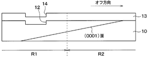
まず、図1Aに示されるように、例えば(0001)Si面に対して主表面の成す角度、つまりオフ角が4°で、オフ方向が<11-20>とされた4H型のSiC単結晶によって構成されたSiC半導体基板10を用意する。以下では、このSiC半導体基板10のうちのアライメントマークを形成する領域をアライメントマーク形成領域R1とし、半導体素子等のデバイスを形成する領域をデバイス形成領域R2とする。
次に、図1Bに示されるように、SiC半導体基板10の主表面にレジスト等のマスク材11を配置し、マスク材11のうちのトレンチ形成予定領域に対応する領域を開口する。そして、SiC半導体基板10をマスク材11で覆った状態で、例えば、RIE(すなわち、Reactive Ion Etching)等の異方性ドライエッチングを行い、アライメントマーク形成領域R1にアライメントマークとなるトレンチ12を形成する。なお、本実施形態では、トレンチ12が第1トレンチおよび第1主トレンチに相当している。
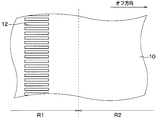
具体的には、図2に示されるように、開口部が長方形状であって長手方向がオフ方向と平行となるトレンチ12を、オフ方向と直交する方向に沿って複数形成する。なお、このトレンチ12のより詳細な形状については、後述する。
続いて、図1Cに示されるように、例えばCVD(すなわち、Chemical Vapor Deposition)法により、SiC半導体基板10にSiCで構成されるエピタキシャル層13を成長させる。これにより、エピタキシャル層13の表面には、下地となるSiC半導体基板10の形状が引き継がれる。このため、エピタキシャル層13の表面には、トレンチ12と対応する位置にトレンチ14が形成される。そして、このトレンチ14が新たなアライメントマークとなる。なお、本実施形態では、トレンチ14が第2トレンチおよび第2主トレンチに相当している。
この際、トレンチ14のうちのオフ方向の下流側では、ファセット面が形成され得るが、ファセット面は、トレンチ14におけるオフ方向と直交する方向の長さに依存して形成される。つまり、オフ方向と直交する方向の長さが短いほどファセット面が形成され難くなる。したがって、本実施形態のように、開口部が長方形状であって長手方向がオフ方向と平行となるようにトレンチ12を形成することにより、ファセット面が形成されることを抑制できる。
なお、エピタキシャル層13は、成長速度が速すぎると3C-SiC欠陥等の欠陥が生成される可能性がある。このため、本実施形態では、エピタキシャル層13は、成長速度が2μm/h以下の条件で成長される。
その後、図示しない読取装置にてアライメントマークとなるトレンチ14を読み取り、デバイス形成領域R2にイオン注入やエッチング等の所定の製造プロセスを行う。
例えば、読取装置にてアライメントマークを読み取る際には、読取装置を走査させながら複数のレーザ光をエピタキシャル層13が形成されたSiC半導体基板10に照射させ、読取装置にてSiC半導体基板10で反射されたレーザ光に含まれる情報を解析する。これにより、トレンチ14の形成位置を特定する。
具体的には、エピタキシャル層13で反射されるレーザ光の強度は、読取装置における光源とエピタキシャル層13との距離に依存し、アライメントマークが形成されている部分では形成されていない部分と比較して距離が長くなって強度が弱くなる。このため、読取装置に、例えば、複数の反射されたレーザ光の強度信号を読み取らせることによりアライメントマークの位置を特定することができる。また、レーザ光の強度が光源とエピタキシャル層13との距離に依存するため、読取装置に、例えば、読み取った強度信号を強度信号が変化するときにピークが表れる信号に変換させることにより、変換した信号に基づいてアライメントマークの位置を特定することもできる。
このとき、アライメントマークとなるトレンチ14にファセット面が形成されていると、ファセット面においてレーザ光が散乱し、読取装置によるアライメントマークの読み取りを高精度に行うことができなくなる。具体的には、アライメントマークの位置を特定する際、ファセット面が形成されていることでオフ方向の位置の特定に位置ズレが生じることがある。このため、エピタキシャル層13上に転写マスクなどのマスクを配置する際等に位置ズレが生じ、高精度なデバイス製造が行えない等の不具合が発生する可能性がある。
しかしながら、本実施形態では、トレンチ12は、開口部がオフ方向と直交する方向を短辺とする長方形状とされている。このため、トレンチ14にファセット面が形成されることが抑制される。したがって、読取装置によるアライメントマークの読み取りを高精度に実行することができる。
そして、このようにしてトレンチ14で形成されるアライメントマークの形成位置を読み取ることにより、エピタキシャル層13へのイオン注入による不純物層の形成工程やトレンチ形成等を行う際のマスクの位置合わせ等を高精度に行うことができる。
次に、本実施形態の各トレンチ12の詳細な形状について、図3および図4を参照しつつ説明する。図3および図4に示されるように、エピタキシャル層13を1.4μm成長させた場合と、エピタキシャル層13を2.1μm成長させた場合とでは、読取可能な範囲が異なり、エピタキシャル層13の膜厚が厚いほど読取可能な範囲が狭くなる。なお、図3および図4中では、ハッチングを施した部分、つまり、共に直線L1~L5で囲まれる部分がトレンチ14を高精度に読み取ることができたトレンチ12の形状となる。
このため、トレンチ12は、成長させるエピタキシャル層13の膜厚も考慮して形状が規定されることが好ましく、下記数式1~5を全て満たすように形成されている。以下では、トレンチ12における長手方向と直交する方向であって、SiC半導体基板10の面方向に沿った方向の長さをトレンチ12の幅wともいい、トレンチ12の深さをトレンチ12の深さdともいう。なお、図2中では、トレンチ12の幅Wは図中の紙面上下方向となる。また、トレンチ14を高精度に読み取ることができない場合には、読取装置で読み取った強度信号中に複数の強度変化のピーク(すなわち、ファセット)が存在することによってトレンチ14を高精度に読み取ることができない場合等が含まれる。さらに、トレンチ14を高精度に読み取ることができない場合には、強度変化自体を明確に読み取ることができない場合等が含まれる。
まず、トレンチ12は、幅wが狭すぎると、エピタキシャル層13を成長させた場合に当該トレンチ12が容易に埋まってしまってエピタキシャル層13にトレンチ14が形成されない。つまり、読取装置にてアライメントマークを読み取ることができない。例えば、図3には、幅wが約1.3μm以上の場合にトレンチ14を正確に読み取ることができる場合があることが示されている。図4には、幅wが約1.95μm以上の場合にトレンチ14を正確に読み取ることができる場合があることが示されている。このため、トレンチ12は、成長させるエピタキシャル層13の膜厚をtとすると、次式を満たすように形成される。
(数1)w≧(1.3/1.4)t=0.93t
なお、直線L1は、w=0.93tとなる。
なお、直線L1は、w=0.93tとなる。
また、トレンチ12は、幅wが多少大きくなっても深さdが浅いと、エピタキシャル層13を成長させた場合に当該トレンチ12が容易に埋まってしまってエピタキシャル層13にトレンチ14が形成されない。つまり、読取装置にてアライメントマークを読み取ることができない。図3には、d≧-0.56w+1.18であればトレンチ14を正確に読み取ることができる場合があることが示されている。図4には、d≧-0.86w+1.76であればトレンチ14を正確に読み取ることができる場合があることが示されている。このため、トレンチ12は、成長させるエピタキシャル層13の膜厚tに基づき、幅wおよび深さdが次式を満たすように形成される。
(数2)d≧(-0.41w+0.84)t
なお、直線L2は、d=(-0.41w+0.84)tとなる。
なお、直線L2は、d=(-0.41w+0.84)tとなる。
さらに、トレンチ12は、深さdが浅すぎると、エピタキシャル層13を成長させた場合に当該トレンチ12が容易に埋まってしまってエピタキシャル層13にトレンチ14が形成されない。つまり、読取装置にてアライメントマークを読み取ることができない。図3には、d≧0.2であればトレンチ14を正確に読み取ることができる場合があることが示されている。図4には、d≧0.29であればトレンチ14を正確に読み取ることができる場合があることが示されている。このため、トレンチ12は、成長させるエピタキシャル層13の膜厚tに基づき、深さdが次式を満たすように形成される。
(数3)d≧(0.2/1.4)t=0.14t
なお、直線L3は、d=0.14tとなる。
なお、直線L3は、d=0.14tとなる。
また、トレンチ12は、幅wが数式1より大きく、深さdが数式3より深くても、読取装置にてトレンチ14を正確に読み取ることができない場合がある。これは、トレンチ12の形状によっては、トレンチ14の開口部の形状がなだらかになってしまい、読取装置にて強度信号の変化を明確に検出できないためである。図3には、d≧0.67w-1.4であればトレンチ14を正確に読み取ることができる場合があることが示されている。図4には、d≧1.0w-2.1であればトレンチ14を正確に読み取ることができる場合があることが示されている。このため、トレンチ12は、成長させるエピタキシャル層13の膜厚tに基づき、幅wおよび深さdが次式を満たすように形成される。
(数4)d≧(0.48w-1.0)t
なお、直線L4は、d=(0.48w-1.0)tとなる。
なお、直線L4は、d=(0.48w-1.0)tとなる。
そして、トレンチ12は、幅wが大きくなり過ぎると、ファセット面が形成される。つまり、読取装置にてアライメントマークを高精度に読み取ることができない。図3および図4には、幅wが約3.0μm以下の場合にトレンチ14を正確に読み取ることができる場合があることが示されている。このため、トレンチ12は、次式を満たすように形成されている。
(数5)w≦3.0
なお、直線L5は、w=3.0となる。
なお、直線L5は、w=3.0となる。
以上より、本実施形態では、上記数式5を満たしつつ、エピタキシャル層13の膜厚tに基づいて上記数式1~数式4を満たすように、トレンチ12が形成されている。
以上説明したように、本実施形態では、開口部が長方形状であって長手方向がオフ方向と平行となるトレンチ12をオフ方向と直交する方向に複数形成している。このため、エピタキシャル層13を成長させた際、各トレンチ12におけるオフ方向の下流側では、ファセット面が形成されることが抑制される。したがって、エピタキシャル層13を成長させた後のトレンチ14をアライメントマークとして高精度に読み取ることができる。また、本実施形態では、新たなトレンチを形成する必要もないため、製造工程が増加したり複雑化したりすることもない。
また、トレンチ12は、幅wが3.0μm以下とされている。このため、トレンチ14にファセット面が形成されることが抑制される。
さらに、トレンチ12は、上記数式1~4を満たすように形成されている。このため、エピタキシャル層13にトレンチ14が形成されないことを抑制でき、またエピタキシャル層13に形成されたトレンチ14が正確に読み取れないことを抑制できる。
(第2実施形態)
第2実施形態について説明する。本実施形態では、アライメントマーク形成領域R1にアライメント検査用マークを形成したものであり、その他に関しては第1実施形態と同様であるため、ここでは説明を省略する。
第2実施形態について説明する。本実施形態では、アライメントマーク形成領域R1にアライメント検査用マークを形成したものであり、その他に関しては第1実施形態と同様であるため、ここでは説明を省略する。
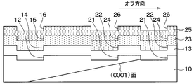
本実施形態では、図5Aに示されるように、トレンチ12を形成する工程では、まず、マスク材11のうちのトレンチ形成予定領域に対応する領域および検査用トレンチ形成予定領域に対応する領域を開口する。そして、SiC半導体基板10をマスク材11で覆った状態で、例えば、RIE等の異方性ドライエッチングを行い、アライメントマーク形成領域R1に、トレンチ12と共に、検査用トレンチ21を形成する。
具体的には、図6に示されるように、検査用トレンチ21は、第1方向用トレンチ21aと第2方向用トレンチ21bとを有している。そして、第1方向用トレンチ21aおよび第2方向用トレンチ21bは、これら第1方向用トレンチ21aおよび第2方向用トレンチ21bで囲まれる領域が略形状となるように形成されている。
より詳しくは、第1方向用トレンチ21aは、トレンチ12と同じ形状とされている。そして、本実施形態では、第1方向用トレンチ21aは、オフ方向と直交する方向に沿って、2列形成されている。第2方向用トレンチ21bは、オフ方向を長手方向とする長方形状とされており、長手方向の長さが第1方向用トレンチ21aよりも大きくされている。そして、第2方向用トレンチ21bは、第1方向用トレンチ21aの配列方向における両端部側に形成されている。なお、本実施形態では、第1方向用トレンチ21aが第1トレンチおよび第1副トレンチに相当している。
次に、図5Bに示されるように、SiC半導体基板10にSiCで構成されるエピタキシャル層13を成長させる。これにより、エピタキシャル層13の表面に、トレンチ14と共に、検査用トレンチ21の形状を引き継ぐ検査用トレンチ22が形成される。なお、本実施形態では、検査用トレンチ22が第2トレンチおよび第2副トレンチに相当している。
その後、図5Cに示されるように、酸化膜等で構成されるパターン形成用膜23をCVD法等で形成する。この際、パターン形成用膜23には、トレンチ14の形状に対応したトレンチ15、および検査用トレンチ22の形状に対応した検査用トレンチ24が形成される。つまり、パターン形成用膜23には、トレンチ14の形状を引き継ぐトレンチ15および検査用トレンチ22の形状を引き継ぐ検査用トレンチ24が形成される。なお、本実施形態では、トレンチ15が第3主トレンチに相当し、検査用トレンチ24が第3副トレンチに相当している。
続いて、パターン形成用膜23上にレジスト25を塗布法等で形成する。この際、レジスト25には、トレンチ15の形状に対応したトレンチ16、および検査用トレンチ24の形状に対応した検査用トレンチ26が形成される。つまり、レジスト25には、トレンチ15の形状を引き継ぐトレンチ16および検査用トレンチ24の形状を引き継ぐ検査用トレンチ26が形成される。なお、本実施形態では、トレンチ16が第4主トレンチに相当し、検査用トレンチ26が第4副トレンチに相当している。
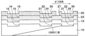
そして、図5Dに示されるように、トレンチ16をアライメントマークとし、レジスト25の露光、現像を行って当該レジスト25をパターニングする。この際、レジスト25にトレンチで構成される検査用パターン27を同時に形成する。なお、本実施形態では、検査用トレンチ26で囲まれる領域内に検査用パターン27を形成する。
次に、図示しない読取装置にて検査用パターン27および検査用トレンチ26をそれぞれ読み込み、検査用パターン27と検査用トレンチ26との間隔を測定することでアライメント精度を検査する。具体的には、図7に示されるように、オフ方向に沿って、第1方向用トレンチ21a上に形成された検査用トレンチ26と検査用パターン27を読み込み、間隔x1、x2を測定する。また、オフ方向と直交する方向に沿って、第2方向用トレンチ21b上に形成された検査用トレンチ26と検査用パターン27を読み込み、間隔y1、間隔y2を測定する。そして、各間隔x1、x2、y1、y2が許容誤差であるか否かを判定し、許容誤差であれば、レジスト25をマスクとしてその後の工程を行う。一方、許容誤差でない場合には、例えば、レジスト25を除去し、再び新たなレジストを形成する。そして、測定した間隔x1、x2、y1、y2を考慮して新たな検査用パターンを形成し、間隔x1、x2、y1、y2が許容誤差となるようにする。
以上説明したように、本実施形態では、開口部が長方形状であって長手方向がオフ方向と平行となる第1方向用トレンチ21aをオフ方向と直交する方向に複数形成している。このため、エピタキシャル層13を成長させた際、各第1方向用トレンチ21aにおけるオフ方向の下流側では、ファセット面が形成されることが抑制される。つまり、エピタキシャル層13上にパターン形成用膜23およびレジスト25を形成した際、第1方向用トレンチ21a上に形成される検査用トレンチ24、26にファセット面が形成されることが抑制される。したがって、第1方向用トレンチ21a上に形成された検査用トレンチ26を高精度に読み取ることができ、特にオフ方向の位置ずれに関するアライメント検査を高精度に行うことができる。
(他の実施形態)
本開示は、実施形態に準拠して記述されたが、本開示は当該実施形態や構造に限定されるものではないと理解される。本開示は、様々な変形例や均等範囲内の変形をも包含する。加えて、様々な組み合わせや形態、さらには、それらに一要素のみ、それ以上、あるいはそれ以下、を含む他の組み合わせや形態をも、本開示の範疇や思想範囲に入るものである。
本開示は、実施形態に準拠して記述されたが、本開示は当該実施形態や構造に限定されるものではないと理解される。本開示は、様々な変形例や均等範囲内の変形をも包含する。加えて、様々な組み合わせや形態、さらには、それらに一要素のみ、それ以上、あるいはそれ以下、を含む他の組み合わせや形態をも、本開示の範疇や思想範囲に入るものである。
例えば、上記各実施形態では、4H型のSiC半導体基板10を例に挙げて説明したが、例えば、6H型、3C型、15R型等の他の多形のSiC半導体基板であっても良い。また、(0001)面に対するオフ角として4°を例に挙げたが、他の角度であっても構わない。
また、上記第2実施形態において、検査用トレンチ21は、第1方向用トレンチ21aのみを有していてもよい。この場合、第1方向用トレンチ21aは、オフ方向と直交する方向に1列のみ形成されていてもよい。
なお、結晶の方位を示す場合、本来ならば所望の数字の上にバー(-)を付すべきであるが、電子出願に基づく表現上の制限が存在するため、本明細書においては、所望の数字の前にバーを付すものとする。
Claims (4)
- 炭化珪素半導体基板(10)の主表面上にエピタキシャル層(13)を形成することを含む炭化珪素半導体装置の製造方法であって、
(0001)面にオフ角が設けられている前記主表面を有すると共に、オフ方向が〈11-20〉である炭化珪素単結晶で構成された前記炭化珪素半導体基板を用意することと、
前記主表面に第1トレンチ(12、21a)を形成することと、
前記主表面の上に、当該主表面に形成された前記第1トレンチの形状を引き継ぐ第2トレンチ(14、22)を有する炭化珪素で構成された前記エピタキシャル層を成長させることと、
前記第2トレンチを読み取って所定の処理を行うことと、を行い、
前記第1トレンチを形成することでは、開口部が長方形状であって長手方向が前記オフ方向と平行とされた前記第1トレンチを前記オフ方向と直交する方向に沿って複数形成する炭化珪素半導体装置の製造方法。 - 前記第1トレンチを形成することでは、前記オフ方向と直交する方向の幅をw[μm]とすると、w≦3.0となる前記第1トレンチを複数形成する請求項1に記載の炭化珪素半導体装置の製造方法。
- 前記第1トレンチを形成することでは、深さをd[μm]、前記エピタキシャル層を成長させることで成長させる前記エピタキシャル層の膜厚をt[μm]とすると、w≧0.93tであり、d≧(-0.41w+0.84)tであり、d≧0.14tであり、かつd≧(0.48w-1.0)tとなる前記第1トレンチを複数形成する請求項2に記載の炭化珪素半導体装置の製造方法。
- 前記第1トレンチを形成することでは、前記第1トレンチとしてアライメントマーク用の第1主トレンチ(12)およびアライメント検査用の第1副トレンチ(21a)をそれぞれ前記オフ方向と直交する方向に沿って複数形成し、
前記エピタキシャル層を成長させることでは、前記第2トレンチとして、前記第1主トレンチの形状を引き継ぐ第2主トレンチ(14)、および前記第1副トレンチの形状を引き継ぐ第2副トレンチ(22)を含む前記エピタキシャル層を成長させ、
前記エピタキシャル層上に、前記第2主トレンチの形状を引き継ぐ第3主トレンチ(15)、および前記第2副トレンチの形状を引き継ぐ第3副トレンチ(24)が形成されたパターン形成用膜(23)を形成することと、
前記パターン形成用膜上に、前記第3主トレンチの形状を引き継ぐ第4主トレンチ(16)、および前記第3副トレンチの形状を引き継ぐ第4副トレンチ(26)が形成されたレジスト(25)を形成することと、
前記レジストに対し、前記第4主トレンチをアライメントマークとして読み取り、前記アライメントマークに基づいて前記レジストに検査用パターン(27)を含む所定のパターンを形成することと、
前記第4副トレンチと前記検査用パターンとの間隔に基づいてアライメント精度を検査することと、を行う請求項1ないし3のいずれか1つに記載の炭化珪素半導体装置の製造方法。
Applications Claiming Priority (2)
| Application Number | Priority Date | Filing Date | Title |
|---|---|---|---|
| JP2017179509A JP2019056725A (ja) | 2017-09-19 | 2017-09-19 | 炭化珪素半導体基板を用いた半導体装置の製造方法 |
| JP2017-179509 | 2017-09-19 |
Publications (1)
| Publication Number | Publication Date |
|---|---|
| WO2019059102A1 true WO2019059102A1 (ja) | 2019-03-28 |
Family
ID=65809874
Family Applications (1)
| Application Number | Title | Priority Date | Filing Date |
|---|---|---|---|
| PCT/JP2018/034054 Ceased WO2019059102A1 (ja) | 2017-09-19 | 2018-09-13 | 炭化珪素半導体基板を用いた半導体装置の製造方法 |
Country Status (2)
| Country | Link |
|---|---|
| JP (1) | JP2019056725A (ja) |
| WO (1) | WO2019059102A1 (ja) |
Citations (7)
| Publication number | Priority date | Publication date | Assignee | Title |
|---|---|---|---|---|
| JPH04127551A (ja) * | 1990-09-19 | 1992-04-28 | Fujitsu Ltd | 露光パターンの検査方法 |
| JP2002031885A (ja) * | 2000-07-17 | 2002-01-31 | Nikon Corp | マスク、露光装置の検査方法、並びに露光方法 |
| JP2003142357A (ja) * | 2001-11-05 | 2003-05-16 | Denso Corp | 半導体装置の製造方法、エピタキシャル膜の膜厚測定方法及び半導体装置 |
| JP2005328014A (ja) * | 2004-04-14 | 2005-11-24 | Denso Corp | 半導体装置の製造方法 |
| JP2008053363A (ja) * | 2006-08-23 | 2008-03-06 | Matsushita Electric Ind Co Ltd | 半導体基板およびその製造方法 |
| JP2009170558A (ja) * | 2008-01-14 | 2009-07-30 | Denso Corp | 炭化珪素半導体装置の製造方法 |
| WO2014199749A1 (ja) * | 2013-06-13 | 2014-12-18 | 住友電気工業株式会社 | 炭化珪素半導体装置の製造方法 |
-
2017
- 2017-09-19 JP JP2017179509A patent/JP2019056725A/ja active Pending
-
2018
- 2018-09-13 WO PCT/JP2018/034054 patent/WO2019059102A1/ja not_active Ceased
Patent Citations (7)
| Publication number | Priority date | Publication date | Assignee | Title |
|---|---|---|---|---|
| JPH04127551A (ja) * | 1990-09-19 | 1992-04-28 | Fujitsu Ltd | 露光パターンの検査方法 |
| JP2002031885A (ja) * | 2000-07-17 | 2002-01-31 | Nikon Corp | マスク、露光装置の検査方法、並びに露光方法 |
| JP2003142357A (ja) * | 2001-11-05 | 2003-05-16 | Denso Corp | 半導体装置の製造方法、エピタキシャル膜の膜厚測定方法及び半導体装置 |
| JP2005328014A (ja) * | 2004-04-14 | 2005-11-24 | Denso Corp | 半導体装置の製造方法 |
| JP2008053363A (ja) * | 2006-08-23 | 2008-03-06 | Matsushita Electric Ind Co Ltd | 半導体基板およびその製造方法 |
| JP2009170558A (ja) * | 2008-01-14 | 2009-07-30 | Denso Corp | 炭化珪素半導体装置の製造方法 |
| WO2014199749A1 (ja) * | 2013-06-13 | 2014-12-18 | 住友電気工業株式会社 | 炭化珪素半導体装置の製造方法 |
Also Published As
| Publication number | Publication date |
|---|---|
| JP2019056725A (ja) | 2019-04-11 |
Similar Documents
| Publication | Publication Date | Title |
|---|---|---|
| TWI427736B (zh) | 改良基板載體效能之方法 | |
| JP6950396B2 (ja) | 炭化珪素半導体基板およびそれを用いた炭化珪素半導体装置の製造方法 | |
| JP2011100928A (ja) | 炭化珪素半導体装置の製造方法 | |
| KR100500469B1 (ko) | 정렬마크와 이를 이용하는 노광정렬시스템 및 그 정렬방법 | |
| JP6153117B2 (ja) | 結晶方位マーク付き処理基板、結晶方位検出方法及び結晶方位マーク読出装置 | |
| JPH0321901B2 (ja) | ||
| JP4772565B2 (ja) | 半導体装置の製造方法 | |
| EP1806770A1 (en) | Gallium nitride wafer | |
| WO2019059102A1 (ja) | 炭化珪素半導体基板を用いた半導体装置の製造方法 | |
| KR100392744B1 (ko) | 반도체 장치, 그 제조에 이용하는 포토마스크, 및 그 중첩정밀도 향상 방법 | |
| JP4531713B2 (ja) | アライメントマーク及びその形成方法、半導体装置及びその製造方法 | |
| JP2013065650A (ja) | 炭化珪素半導体装置の製造方法 | |
| US20050244729A1 (en) | Method of measuring the overlay accuracy of a multi-exposure process | |
| US20040135232A1 (en) | Semiconductor wafer and method of marking a crystallographic direction on a semiconductor wafer | |
| CN102931219B (zh) | 半导体器件及其制备方法 | |
| JP4626909B2 (ja) | 半導体ウエハ | |
| KR100859493B1 (ko) | 반도체 소자의 제조방법 | |
| KR100866747B1 (ko) | 반도체 소자의 오버레이 버니어 및 그 형성 방법 | |
| US7236245B2 (en) | Overlay key with a plurality of crossings and method of measuring overlay accuracy using the same | |
| US20230275033A1 (en) | Semiconductor substrate having an alignment structure | |
| JP4225358B2 (ja) | 半導体装置及び半導体装置の製造方法 | |
| JPS59165421A (ja) | 半導体装置の位置合わせマ−ク | |
| JPS63307727A (ja) | 化合物半導体ウエ−ハのマスク合わせ方法 | |
| CN119937263A (zh) | 一种零层光刻对准标记的制作方法及半导体结构 | |
| KR100352836B1 (ko) | 반도체 소자의 중첩 정밀도 측정 마크 |
Legal Events
| Date | Code | Title | Description |
|---|---|---|---|
| 121 | Ep: the epo has been informed by wipo that ep was designated in this application |
Ref document number: 18858660 Country of ref document: EP Kind code of ref document: A1 |
|
| NENP | Non-entry into the national phase |
Ref country code: DE |
|
| 122 | Ep: pct application non-entry in european phase |
Ref document number: 18858660 Country of ref document: EP Kind code of ref document: A1 |