WO2019044488A1 - 水晶振動子 - Google Patents
水晶振動子 Download PDFInfo
- Publication number
- WO2019044488A1 WO2019044488A1 PCT/JP2018/030254 JP2018030254W WO2019044488A1 WO 2019044488 A1 WO2019044488 A1 WO 2019044488A1 JP 2018030254 W JP2018030254 W JP 2018030254W WO 2019044488 A1 WO2019044488 A1 WO 2019044488A1
- Authority
- WO
- WIPO (PCT)
- Prior art keywords
- electrode
- sealing material
- conductive sealing
- quartz substrate
- main surface
- Prior art date
- Legal status (The legal status is an assumption and is not a legal conclusion. Google has not performed a legal analysis and makes no representation as to the accuracy of the status listed.)
- Ceased
Links
Images





Classifications
-
- H—ELECTRICITY
- H03—ELECTRONIC CIRCUITRY
- H03H—IMPEDANCE NETWORKS, e.g. RESONANT CIRCUITS; RESONATORS
- H03H9/00—Networks comprising electromechanical or electro-acoustic elements; Electromechanical resonators
- H03H9/15—Constructional features of resonators consisting of piezoelectric or electrostrictive material
- H03H9/17—Constructional features of resonators consisting of piezoelectric or electrostrictive material having a single resonator
- H03H9/19—Constructional features of resonators consisting of piezoelectric or electrostrictive material having a single resonator consisting of quartz
-
- H—ELECTRICITY
- H03—ELECTRONIC CIRCUITRY
- H03H—IMPEDANCE NETWORKS, e.g. RESONANT CIRCUITS; RESONATORS
- H03H9/00—Networks comprising electromechanical or electro-acoustic elements; Electromechanical resonators
- H03H9/02—Details
- H03H9/05—Holders or supports
- H03H9/10—Mounting in enclosures
- H03H9/1007—Mounting in enclosures for bulk acoustic wave [BAW] devices
- H03H9/1035—Mounting in enclosures for bulk acoustic wave [BAW] devices the enclosure being defined by two sealing substrates sandwiching the piezoelectric layer of the BAW device
-
- H—ELECTRICITY
- H03—ELECTRONIC CIRCUITRY
- H03H—IMPEDANCE NETWORKS, e.g. RESONANT CIRCUITS; RESONATORS
- H03H9/00—Networks comprising electromechanical or electro-acoustic elements; Electromechanical resonators
- H03H9/02—Details
- H03H9/02007—Details of bulk acoustic wave devices
- H03H9/02086—Means for compensation or elimination of undesirable effects
- H03H9/02094—Means for compensation or elimination of undesirable effects of adherence
-
- H—ELECTRICITY
- H03—ELECTRONIC CIRCUITRY
- H03H—IMPEDANCE NETWORKS, e.g. RESONANT CIRCUITS; RESONATORS
- H03H9/00—Networks comprising electromechanical or electro-acoustic elements; Electromechanical resonators
- H03H9/02—Details
- H03H9/05—Holders or supports
-
- H—ELECTRICITY
- H03—ELECTRONIC CIRCUITRY
- H03H—IMPEDANCE NETWORKS, e.g. RESONANT CIRCUITS; RESONATORS
- H03H9/00—Networks comprising electromechanical or electro-acoustic elements; Electromechanical resonators
- H03H9/02—Details
- H03H9/125—Driving means, e.g. electrodes, coils
- H03H9/13—Driving means, e.g. electrodes, coils for networks consisting of piezoelectric or electrostrictive materials
Definitions
- the present invention relates to a quartz oscillator used for timing devices, load sensors and the like.
- the piezoelectric vibrator is mounted on a mobile communication device or the like, and is used as, for example, a timing device or a load sensor.
- a quartz oscillator which is a type of piezoelectric oscillator, uses artificial quartz for the piezoelectric body and has high frequency accuracy. With the miniaturization of electronic devices in recent years, miniaturization of crystal units is also required.
- Patent Document 1 a process of forming an electrode pad and a connection electrode, a process of joining two package members by a sealing material formed on both sides of a quartz substrate, and a laser beam from outside the package member And irradiating the connection electrode, and connecting the electrode pad and the connection electrode to form an internal wiring conductor.
- the internal wiring conductor is one in which an electrode pad and a connection electrode are integrated, and is electrically connected to a via electrode penetrating the exterior member. According to this, it is possible to reliably connect the wiring conductors while responding to the reduction in height of the quartz oscillator.
- interposed by such two exterior members is called sandwich structure below.
- a crystal unit is considered in which the extraction electrode and the conductive sealing material are integrally formed, and a voltage is applied to the excitation electrode through the conductive sealing material.
- a quartz oscillator can omit a through hole, and can be miniaturized.
- the voltage is also applied to the conductive sealing material when applying a voltage to the excitation electrode, so that the conductive materials facing each other across the quartz substrate Sealing material may cause unnecessary vibration. Such unnecessary vibration propagates through the quartz substrate and degrades the vibration characteristics of the quartz oscillator.
- the present invention has been made in view of such circumstances, and it is an object of the present invention to provide a quartz oscillator capable of suppressing the deterioration of vibration characteristics while reducing the size.
- a quartz oscillator comprises a quartz substrate having a first main surface and a second main surface facing each other, a first excitation electrode provided on the first main surface of the quartz substrate, and a quartz substrate.
- a second excitation electrode provided on the second main surface and facing the first excitation electrode with the quartz substrate interposed therebetween, and a first conductive sealing material provided on the first main surface of the quartz substrate and surrounding the first excitation electrode;
- the second conductive sealing material is provided on the second main surface of the quartz substrate and is joined to the quartz substrate with the second conductive sealing material surrounding the second excitation electrode and the first conductive sealing material, and the first excitation electrode is A first exterior member for covering, and a second exterior member which is joined to the quartz substrate with the second conductive sealing material interposed therebetween and which opens the space to cover the second excitation electrode, and the first main surface of the quartz substrate is provided
- a first lead-out electrode electrically connecting the first excitation electrode and the first conductive sealing material, and the second principal surface of the quartz substrate is provided with a first lead
- a second lead-out electrode electrically connecting the second conductive sealing material to the second conductive sealing material, and at least a portion of the first conductive sealing material, when the first main surface of the quartz substrate is viewed in plan,
- the first lead-out electrode is located outside the second conductive sealing material, and intersects the second conductive sealing material with the quartz substrate interposed therebetween.
- the present invention it is possible to provide a quartz oscillator capable of suppressing the deterioration of the vibration characteristics while reducing the size.
- FIG. 1 is an exploded perspective view schematically showing the configuration of a quartz oscillator according to the first embodiment.
- FIG. 2 is a perspective view schematically showing the configuration of the crystal unit shown in FIG.
- FIG. 3 is a cross-sectional view schematically showing a configuration of a cross section taken along line III-III of the quartz oscillator shown in FIG.
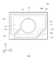
- FIG. 4 is a plan view schematically showing the configuration of the crystal substrate according to the first embodiment.
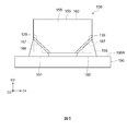
- FIG. 5 is a view schematically showing an example of a mounting aspect of the crystal unit according to the first embodiment on an external substrate.
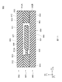
- FIG. 6 is a plan view schematically showing the configuration of a quartz substrate according to a second embodiment.
- FIG. 7 is a plan view schematically showing the configuration of a quartz substrate according to a third embodiment.
- FIG. 8 is a plan view schematically showing the configuration of a crystal unit according to a fourth embodiment.
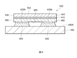
- FIG. 9 is a view schematically showing an example of a mounting aspect of the crystal unit according to the fourth embodiment on an external substrate.
- FIG. 10 is an exploded perspective view schematically showing a configuration of a crystal unit according to a fifth embodiment.
- FIG. 11 is a cross-sectional view schematically showing a configuration of a crystal unit according to a fifth embodiment.
- FIG. 1 is an exploded perspective view schematically showing the configuration of a quartz oscillator according to the first embodiment.
- FIG. 2 is a perspective view schematically showing the configuration of the crystal unit shown in FIG.
- FIG. 3 is a cross-sectional view schematically showing a configuration of a cross section taken along line III-III of the quartz oscillator shown in FIG.
- FIG. 4 is a plan view schematically showing the configuration of the crystal substrate according to the first embodiment.
- first direction D1, the second direction D2 and the third direction D3 shown in the drawing are directions orthogonal to each other, the present invention is not limited to this as long as they are directions intersecting each other, The directions may cross each other at an angle other than 90 °.
- a quartz crystal resonator unit (Quartz Crystal Resonator Unit) 100 is a type of piezoelectric vibrator, and excites a quartz crystal resonator element (Quartz Crystal Resonator) 101 according to an applied voltage.
- the crystal vibrating element 101 utilizes a quartz crystal element (Quartz Crystal Element) as a piezoelectric body that vibrates according to an applied voltage.
- the crystal unit 100 includes a crystal vibrating element 101, a first exterior member 150, and a second exterior member 160.
- the crystal unit 100 has a so-called sandwich structure in which the crystal vibrating element 101 is sandwiched between the first exterior member 150 and the second exterior member 160.
- the quartz crystal vibrating element 101 includes a plate-like quartz crystal substrate 110.
- the quartz substrate 110 has a first main surface 110A and a second main surface 110B facing each other.
- the first major surface 110A is located on the side facing the first exterior member 150
- the second major surface 110B is located on the side facing the second exterior member 160.
- the quartz substrate 110 is, for example, an AT-cut-type quartz piece.
- the AT cut type crystal piece has a plane parallel to the plane specified by the X axis and the Z 'axis (hereinafter referred to as "XZ' plane". The same applies to the planes specified by the other axes).
- It is a flaky crystal of quartz cut out of artificial quartz so as to be a main surface.
- the X-axis, Y-axis and Z-axis are crystal axes of artificial quartz, and the Y'-axis and Z'-axis are Y-axis and Z-axis respectively in the direction from Y-axis to Z-axis It is an axis rotated at 35 degrees 15 minutes ⁇ 1 minute 30 seconds.
- the first major surface 110A and the second major surface 110B respectively correspond to the XZ ′ plane.
- the cut angle of a crystal piece may apply different cut (for example, BT cut etc.) other than AT cut.
- the AT cut type crystal substrate 110 has a long side direction in which a long side parallel to the X axis direction extends, a short side direction in which a short side parallel to the Z ′ axis direction extends, and a parallel side in the Y ′ axis direction. Thickness has an extending thickness direction.
- the quartz substrate 110 has a rectangular shape when the first main surface 110A is viewed in plan, and includes an excitation portion 111 located at the center and contributing to excitation and a peripheral portion 112 surrounding the excitation portion 111. .
- the excitation portion 111 and the peripheral portion 112 are continuous, and the crystal substrate 110 has a flat plate structure in which the thickness of the excitation portion 111 and the thickness of the peripheral portion 112 are substantially uniform.
- the crystal substrate 110 is not limited to this as long as it has a plate shape.
- the excitation portion 111 may have a mesa structure thicker than the peripheral portion 112.
- the quartz substrate 110 may have a reverse mesa structure in which the excitation portion 111 is thinner than the peripheral portion 112, and has a convex shape or a bevel shape in which the thicknesses of the excitation portion 111 and the peripheral portion 112 change continuously. It is also good.
- the quartz substrate 110 has a plate shape, the excitation portion 111 of the quartz substrate 110 is easily deformed by a load acting from the outside of the quartz oscillator 100, so the vibration characteristics change sensitively according to the load. Therefore, the crystal unit 100 suitable for a load sensor can be provided. As described later, a slit may be formed between the excitation portion 111 and the peripheral portion 112.
- the X axis is parallel to the first direction D1
- the Z 'axis is parallel to the second direction D2
- the Y' axis is parallel to the third direction D3. It is arranged to become.
- the quartz crystal vibrating element using the AT-cut type quartz crystal piece has high frequency stability in a wide temperature range and is excellent in aging characteristics, and can be manufactured at low cost. Therefore, it can be suitably used as a timing device. Moreover, since it is sensitive to the load from the outside and the excitation frequency changes according to the strain, it can be suitably used as a load sensor.
- the AT cut type quartz crystal vibrating element is used as a main vibration in a thickness shear vibration mode (Thickness Shear Mode).
- the quartz crystal vibrating element 101 includes a first excitation electrode 121 and a second excitation electrode 131 which constitute a pair of electrodes.
- the first excitation electrode 121 and the second excitation electrode 131 are provided in the excitation unit 111.
- the first excitation electrode 121 is provided on the first major surface 110 ⁇ / b> A of the quartz substrate 110.
- the second excitation electrode 131 is provided on the second major surface 110 B of the quartz substrate 110.
- the first excitation electrode 121 and the second excitation electrode 131 are provided to face each other with the quartz substrate 110 interposed therebetween.
- the first excitation electrode 121 and the second excitation electrode 131 are arranged such that substantially the whole overlap in the XZ ′ plane.
- the first excitation electrode 121 and the second excitation electrode 131 are respectively provided in a circular shape when the first main surface 110A and the second main surface 110B are viewed in plan.
- the first excitation electrode 121 and the second excitation electrode 131 are not limited to the above, and may have a polygonal shape, an elliptical shape, or a shape combining these, for example, a rectangular shape.
- the quartz crystal vibrating element 101 includes a first conductive sealing material 123 and a second conductive sealing material 133 having conductivity.
- the first conductive sealing material 123 and the second conductive sealing material 133 are provided on the peripheral portion 112 of the quartz substrate 110.
- the first conductive sealing material 123 is provided on the first major surface 110 ⁇ / b> A of the quartz substrate 110.
- the first conductive sealing material 123 is formed in a frame shape surrounding the first excitation electrode 121 when the first main surface 110A is viewed in plan.
- the second conductive sealing material 133 is provided on the second major surface 110 ⁇ / b> B of the quartz substrate 110.
- the second conductive sealing material 133 is formed in a frame shape surrounding the second excitation electrode 131 when the second main surface 110B is viewed in plan.
- the quartz crystal vibrating element 101 includes a first extraction electrode 125 and a second extraction electrode 135.
- the first lead electrode 125 is provided on the first major surface 110 ⁇ / b> A of the quartz substrate 110.
- the first lead-out electrode 125 electrically connects the first excitation electrode 121 and the first conductive sealing material 123.
- the second lead electrode 135 is provided on the second major surface 110 ⁇ / b> B of the quartz substrate 110.
- the second lead-out electrode 135 electrically connects the second excitation electrode 131 and the second conductive sealing material 133.
- the crystal vibrating element 101 includes a first connection electrode 127 and a second connection electrode 137.
- the first connection electrode 127 and the second connection electrode 137 are provided at the peripheral portion 112 of the quartz substrate 110.
- the first connection electrode 127 is provided on the first major surface 110 ⁇ / b> A of the quartz substrate 110.
- the second connection electrode 137 is provided on the second main surface 110 ⁇ / b> B of the quartz substrate 110.
- the first connection electrode 127 is continuous with the first conductive sealing material 123. In other words, the first connection electrode 127 forms a part of the first conductive sealing material 123. In addition, the first lead electrode 125 is directly connected to the first connection electrode 127.
- the second connection electrode 137 is provided on the outer side away from the second conductive sealing material 133, and is electrically connected to the second conductive sealing material 133 by the third lead electrode 136.
- the third lead electrode 136 is provided on the second major surface 110 ⁇ / b> B of the quartz substrate 110. That is, the first connection electrode 127 is electrically connected to the first conductive sealing material 123, and the second connection electrode 137 is electrically connected to the second conductive sealing material 133.
- the first connection electrode 127 and the second connection electrode 137 are limited to the above configuration as long as they are electrically connected to the first conductive sealing material 123 and the second conductive sealing material 133, respectively. is not.
- the first connection electrode 127 may be separated from the first conductive sealing material 123, and the first connection electrode 127 and the first conductive sealing material 123 may be electrically connected by the lead-out electrode.
- the third lead-out electrode 136 may be omitted, and the second connection electrode 137 may be continuous with the second conductive sealing material 133.
- an electrode group including the first excitation electrode 121, the first conductive sealing material 123, the first lead electrode 125, and the first connection electrode 127 is formed on the first major surface 110A of the quartz substrate 110.
- An electrode group including the second excitation electrode 131, the second conductive sealing material 133, the second lead electrode 135, and the second connection electrode 137 is formed on the second main surface 110B of the quartz substrate 110. .
- the first conductive sealing material 123 and the second conductive sealing material 133 are separated, the first extraction electrode 125 and the second extraction electrode 135 are separated, and the first connection electrode 127 and the second connection electrode 137 are is seperated.
- the first conductive sealing material 123 does not overlap with the second conductive sealing material 133, so it is located outside the second conductive sealing material 133, that is, on the side away from the excitation portion 111. It is provided. That is, the second conductive sealing material 133 surrounds the first excitation electrode 121 and the second excitation electrode 131, and the first conductive sealing material 123 surrounds the second conductive sealing material 133. According to this, the excitation of the quartz substrate 110 between the first conductive sealing material 123 and the second conductive sealing material 133 is suppressed, and the mixing of unnecessary vibration into the vibration in the excitation portion 111 is reduced. be able to. In addition, as an aspect different from the example shown in FIG.
- the first conductive sealing material 123 and the second conductive sealing material 133 overlap each other if at least a part does not overlap each other. May be For example, a part of the inner side of the first conductive sealing material 123 overlaps the second conductive sealing material 133, and a part of the outer side of the first conductive sealing material 123 is the second conductive sealing material 133 It may be a non-overlapping arrangement.
- the first connection electrode 127 and the second connection electrode 137 are provided at the end of the quartz substrate 110. Specifically, the first connection electrode 127 is disposed at a corner formed by the short side of the quartz substrate 110 in the negative direction D1 and the long side in the negative direction D2.
- the second connection electrode 137 is disposed at a corner formed by the short side of the crystal substrate 110 in the positive direction D1 and the long side in the negative direction of the second direction D2. That is, the first connection electrode 127 and the second connection electrode 137 are provided on the same side of the quartz substrate 110. According to this, it is possible to suppress the excitation of the quartz crystal substrate 110 between the first connection electrode 127 and the second connection electrode 137, and to reduce the mixing of the unnecessary vibration into the vibration in the excitation unit 111.
- the first connection electrode 127 and the second connection electrode 137 are not limited to the above as long as they extend to the end of the quartz substrate 110, and may be provided at diagonally opposite corners. , And may be provided at a central portion of the edge remote from the
- the second connection electrode 137 is disposed outside the first conductive sealing material 123 so as not to overlap with the first conductive sealing material 123. According to this, it is possible to suppress the excitation of the quartz crystal substrate 110 between the second connection electrode 137 and the first conductive sealing material 123.
- the second connection electrode 137 and the first conductive sealing material 123 may be disposed so that at least a part of each other does not overlap. For example, a part of the second connection electrode 137 on the excitation portion 111 side overlaps the first conductive sealing material 123, and the other part of the second connection electrode 137 does not overlap the first conductive sealing material 123. It may be arranged.
- first connection electrode 127 is disposed outside the second conductive sealing material 133 so as not to overlap with the second conductive sealing material 133, but the first connection electrode 127 and the second conductive property are not
- the sealing material 133 may be disposed so that at least a part of each does not overlap.
- the first lead-out electrode 125 extends in the direction connecting the first excitation electrode 121 and the first connection electrode 127, and the second lead-out electrode 135 connects the second excitation electrode 131 and the second connection electrode 137. It extends in the direction. That is, the first extraction electrode 125 and the second extraction electrode 135 extend in different directions as viewed from the excitation unit 111.
- the third lead-out electrode 136 is aligned with the second lead-out electrode 135 on the same straight line. According to this, it is possible to suppress the excitation of the quartz crystal substrate 110 between the first extraction electrode 125 and the second extraction electrode 135, and to reduce the mixing of the unnecessary vibration into the vibration in the excitation portion 111.
- the first lead-out electrode 125 intersects the second conductive sealing material 133 at one point with the quartz substrate 110 interposed therebetween.
- the third lead electrode 136 intersects the first conductive sealing material 123 at one point with the quartz substrate 110 interposed therebetween. According to this, the facing area of the electrode group on the first main surface 110A side and the electrode group on the second main surface 110B side can be reduced. That is, the excitation of the unnecessary vibration in the peripheral portion 112 can be suppressed, and the mixing of the unnecessary vibration into the vibration in the excitation unit 111 can be reduced.
- the first lead electrode 125 and the second conductive sealing material 133 are substantially orthogonal to each other, and the third lead electrode 136 and the first conductive sealing material 123 are substantially orthogonal to each other. As a result, the facing area between the electrode group on the first main surface 110A and the electrode group on the second main surface 110B can be further reduced.
- the electrode group formed on the first major surface 110A of the quartz substrate 110 is integrally formed of the same material.
- An electrode group formed on the second major surface 110B of the quartz substrate 110 is also integrally formed of the same material.
- the material of each electrode group is not particularly limited.
- a chromium (Cr) layer is provided on the side in contact with the quartz substrate 110 as an underlayer, and the layer further away from the quartz substrate 110 than the underlayer as a surface layer. Have a gold (Au) layer.
- the adhesion between the quartz substrate 110 and the electrode group is improved by providing a metal layer having high reactivity with oxygen in the underlayer, and the excitation electrode is deteriorated by providing a metal layer having low reactivity with oxygen in the surface layer.
- the electrical reliability is improved.
- the first exterior member 150 corresponds to one of a pair of holders that accommodates the excitation portion 111 of the quartz crystal substrate 110.
- the first exterior member 150 has a concave shape, and has a box shape opened toward the first main surface 110A of the quartz substrate 110.
- the first exterior member 150 is bonded to the crystal substrate 110 with the first conductive sealing material 123 interposed therebetween, and the internal space 115 is opened to cover the first excitation electrode 121.
- the shape of the first exterior member 150 is not particularly limited as long as the excitation portion 111 can excite.
- the shape of the first exterior member 150 is a flat plate having a planar main surface facing the quartz substrate 110, the quartz substrate 110 It may be in the form of a cylinder, etc., which can be accommodated inside.
- the first exterior member 150 includes a top wall 151 and a side wall 152.
- the top wall portion 151 is opposed to the first major surface 110 ⁇ / b> A of the quartz substrate 110.
- Side wall portion 152 is connected to the outer edge of top wall portion 151 and extends in a direction intersecting the main surface of top wall portion 151.
- the first exterior member 150 has an opposing surface 153, an inner surface 154, an outer major surface 155, and an outer surface 156.
- the opposing surface 153 is a surface of the quartz substrate 110 that faces the first major surface 110A of the peripheral portion 112 at the tip of the side wall portion 152, and the first excitation when the first major surface 110A of the quartz substrate 110 is viewed in plan. It extends in a frame shape so as to surround the electrode 121.
- the inner surface 154 is located on the inner space 115 side of the top wall portion 151 and the side wall portion 152, and an inner main surface and a first excitation electrode overlapping the first main surface 110A when the first main surface 110A of the quartz substrate 110 is viewed in plan.
- the outer major surface 155 is located on the opposite side to the internal space 115 of the top wall portion 151, and is a surface overlapping with the first major surface 110A when the first major surface 110A of the quartz substrate 110 is viewed in plan.
- the outer side surface 156 is located on the opposite side of the inner space 115 of the side wall portion 152 and is a surface connecting the opposing surface 153 and the outer major surface 155.
- a first terminal portion 157 is formed in the first exterior member 150.
- the first terminal portion 157 is a structure for exposing at least a part of the first connection electrode 127.
- the first terminal portion 157 is a recess formed at a corner of the first exterior member 150 when the outer major surface 155 of the first exterior member 150 is viewed in plan, and is connected to the outer side surface 156. That is, the first terminal portion 157 exposes at least a part of the first connection electrode 127 from the end of the first exterior member 150.
- the first terminal portion 157 is formed along the third direction D3 so as to extend from the facing surface 153 side to the outer major surface 155 side.
- the second exterior member 160 corresponds to the other of the pair of holders accommodating the excitation portion 111 of the crystal substrate 110.
- the second exterior member 160 is concave like the first exterior member 150, and has a box shape opened toward the second major surface 110B of the quartz substrate 110.
- the second exterior member 160 is joined to the quartz substrate 110 with the second conductive sealing material 133 interposed therebetween, and the second exterior member 160 opens the internal space 116 to cover the second excitation electrode 131.
- the 2nd exterior member 160 is the structure similar to the 1st exterior member 150, the detailed description of a structure is abbreviate
- the second exterior member 160 includes a top wall portion 161 and a side wall portion 162.
- the top wall portion 161 faces the second main surface 110 ⁇ / b> B of the quartz substrate 110.
- Side wall portion 162 is connected to the outer edge of top wall portion 161 and extends in a direction intersecting the main surface of top wall portion 161.
- the second exterior member 160 has an opposing surface 163, an inner surface 164, an outer major surface 165, and an outer surface 166.
- the opposing surface 163 is a surface of the quartz crystal substrate 110 that faces the second major surface 110 ⁇ / b> B of the peripheral portion 112.
- the inner surface 164 is a surface located on the inner space 116 side of the top wall portion 161 and the side wall portion 162.
- the outer main surface 165 is a surface located on the opposite side to the inner space 116 of the top wall 151.
- the outer side surface 166 is a surface connecting the opposing surface 163 and the outer major surface 165.
- the second terminal portion 167 is also formed on the second exterior member 160.
- the second terminal portion 167 is a structure for exposing at least a part of the second connection electrode 137.
- the first terminal portion 157 is a recess formed at a corner of the second exterior member 160 when the outer major surface 155 of the first exterior member 150 is viewed in plan, and is connected to the outer side surface 166.
- the second terminal portion 167 is formed along the third direction D3 so as to extend from the facing surface 163 side to the outer major surface 165 side.
- the first exterior member 150 and the second exterior member 160 are formed of the same material as that constituting the quartz substrate 110, that is, artificial quartz. According to this, it is possible to suppress the distortion caused by the difference in thermal expansion coefficient between the first exterior member 150 and the second exterior member 160 and the quartz substrate 110.
- One of the first exterior member 150 and the second exterior member 160 may be formed of artificial quartz, and the other may be formed of a material different from artificial quartz. According to this, it is possible to suppress distortion due to the difference in thermal expansion coefficient between at least one of the exterior members and the quartz substrate.
- the material which comprises the 1st exterior member 150 and the 2nd exterior member 160 is not limited to a quartz crystal.
- the first exterior member 150 and the second exterior member 160 may be formed of ceramic. In that case, it is desirable that the thermal expansion coefficient be formed of ceramic close to quartz.
- the first terminal portion 157 and the second terminal portion 167 are formed on the same side of the crystal substrate 110 so as to overlap with different corner portions of the crystal substrate 110 when the first main surface 110A of the crystal substrate 110 is viewed in plan. It is done. That is, the first terminal portion 157 and the second terminal portion 167 are arranged along the long side of the quartz substrate 110 in the second direction D2 negative direction side.
- the corner where the first terminal portion 157 and the second terminal portion 167 are formed is not limited to the second direction D2 negative direction side, and the second direction D2 positive direction side, the first direction D1 positive direction It may be the side and the first direction D1 negative direction side.
- the first terminal portion 157 and the second terminal portion 167 may be formed to overlap corner portions of the crystal substrate 110 located diagonally, and are formed in a central portion of an edge away from the corner portions. It is also good.
- the location to be formed is not limited to the corner portion.
- the first connection electrode 127 is provided at the central portion of the end side (long side or short side in the case of the rectangular crystal substrate 110) away from the corner of the quartz substrate 110
- the first terminal portion 157 is The outer main surface 155 of the first exterior member 150 may be formed at the center of the edge of the first exterior member 150 when viewed in plan.
- the second terminal portion 167 is a second when the outer major surface 165 of the second exterior member 160 is viewed in plan You may form in the edge-central part of the exterior member 160.
- the first terminal portion 157 may be a recess formed on the opposing surface 153 side and separated from the outer major surface 155, and the second terminal portion 167 may be formed on the opposing surface 163 side away from the outer major surface 165. It may be a dent.
- first terminal portion 157 may be a through hole penetrating the side wall portion 152 of the first exterior member 150
- second terminal portion 167 is a through hole penetrating the side wall portion 162 of the second exterior member 160. It may be
- the opposing surface 153 of the first exterior member 150 is joined to the first major surface 110A of the peripheral portion 112 of the quartz substrate 110 with the first conductive sealing material 123 interposed therebetween.
- the first exterior member 150 seals the first excitation electrode 121 in the internal space 115 so that the excitation portion 111 of the quartz substrate 110 can be excited.
- the opposing surface 163 of the second exterior member 160 is bonded to the second major surface 110 B of the peripheral portion 112 of the quartz substrate 110 with the second conductive sealing material 133 interposed therebetween.
- the second exterior member 160 seals the second excitation electrode 131 in the internal space 116 so that the excitation portion 111 of the quartz substrate 110 can be excited.
- At least one member may be provided between the facing surface 153 of the first exterior member 150 and the first major surface 110A of the quartz substrate 110.
- a metallized layer may be formed on the facing surface 153 of the first exterior member 150 to improve the adhesion to a metal.
- a brazing material made of a eutectic gold-tin (Au-Sn) alloy may be provided on the first conductive sealing material 123.
- a metallized layer, a brazing material, or the like may be provided between the facing surface 163 of the second exterior member 160 and the second major surface 110 B of the quartz substrate 110.
- the pressure in the inner space 115 and the inner space 116 is preferably in a vacuum state lower than atmospheric pressure. According to this, it is possible to reduce the temporal fluctuation of the vibration characteristic of the crystal unit 100 caused by the weight change due to the oxidation of the first excitation electrode 121 and the second excitation electrode 131. In addition, it is possible to suppress the operation failure of the crystal unit 100 caused by the decrease in the conductivity due to the oxidation of the first extraction electrode 125 and the second extraction electrode 135.
- the residual gas in the inner space 115 and the inner space 116 is, for example, air containing oxygen (O 2 ), but it may be an inert gas having a low reactivity with metal, a reducing gas having a high reactivity with oxygen, etc. It may be substituted. According to this, oxidation of various electrodes can be suppressed.
- the first exterior member 150 is not limited to the above-mentioned concave shape as long as it can form the internal space 115 with the first excitation electrode 121.
- the second exterior member 160 is not limited to the above-described concave shape as long as the internal space 116 can be formed between the second exterior member 160 and the second excitation electrode 131.
- the peripheral portion 112 of the quartz substrate 110 is thicker than the excitation portion 111, at least one of the first exterior member 150 and the second exterior member 160 may be flat.
- a first external electrode 129 and a second external electrode 139 electrically connected to the first excitation electrode 121 and the second excitation electrode 131 are formed.
- the first outer electrode 129 covers a part of the outer major surface 155 and the outer surface 156 of the first exterior member 150 and covers the first terminal portion 157. Furthermore, the first outer electrode 129 covers a part of the outer major surface 165 and the outer surface 166 of the second exterior member 160.
- the second outer electrode 139 covers a part of the outer major surface 165 and the outer side surface 166 of the second exterior member 160 and covers the second terminal portion 167. Furthermore, the second outer electrode 139 covers a part of the outer major surface 155 and the outer surface 156 of the first exterior member 150.
- the first external electrode 129 can be electrically connected to the first connection electrode 127 at the end of the crystal vibrating element 101 without providing the via hole in the first exterior member 150.
- the second external electrode 139 can be electrically connected to the second connection electrode 137 at the end of the crystal vibrating element 101 without providing a via hole in the second exterior member 160. Therefore, it is possible to suppress the decrease in the airtightness of the internal space 115 and the internal space 116, and to suppress the decrease in the mechanical strength of the first exterior member 150 and the second exterior member 160.
- the first external electrode 129 covers the portion of the first connection electrode 127 exposed from the first exterior member 150 by the first terminal portion 157.
- the second excitation electrode 131 covers a portion of the second connection electrode 137 exposed from the second exterior member 160 by the second terminal portion 167. According to this, the contact area between the first external electrode 129 and the first connection electrode 127 can be enlarged. Therefore, the electrical connection between the first outer electrode 129 and the first connection electrode 127 can be stabilized. Further, the contact area between the second external electrode 139 and the second connection electrode 137 can be enlarged, and the electrical connection between the second external electrode 139 and the second connection electrode 137 can be stabilized.
- the first external electrode 129 and the second external electrode 139 overlap with parts of the first connection electrode 127 and the second connection electrode 137, respectively. Therefore, when the first main surface 110A of the crystal substrate 110 is viewed in plan, the crystal substrate It is provided at the corner of 110. According to this, compared to the configuration in which the first connection electrode 127 and the first external electrode 129 are provided at the center of the edge of the quartz substrate 110, the distance between the first external electrode 129 and the first excitation electrode 121 is It can be extended. Therefore, the vibration leakage from the excitation part 111 which propagates the 1st extraction electrode 125 can be suppressed. Similarly, it is possible to suppress vibration leakage from the excitation unit 111 propagating through the second extraction electrode 135.
- first external electrode 129 and the second external electrode 139 are arranged at the same end of the quartz substrate 110, specifically, the end along the longer side in the second direction D2 negative direction. According to this, with the side on which the first external electrode 129 and the second external electrode 139 are provided facing the external substrate, the first main surface 110A and the second main surface 110B of the crystal substrate 110 stand against the external substrate
- the crystal unit 100 can be mounted in a so-called vertical arrangement.
- the arrangement of the first external electrode 129 and the second external electrode 139 is not limited as long as the first external electrode 129 and the second external electrode 139 are electrically connected to the first connection electrode 127 and the second connection electrode 137, respectively. It may be provided at a corner located at the center of the edge side away from the corner.
- an alternating voltage is applied between the first excitation electrode 121 and the second excitation electrode 131 through the first external electrode 129 and the second external electrode 139.
- the excitation portion 111 of the quartz substrate 110 vibrates in a predetermined vibration mode such as a thickness shear vibration mode, and vibration characteristics associated with the vibration can be obtained.
- the crystal oscillator 100 can be used as a timing device that vibrates at a specific frequency by utilizing this vibration characteristic.
- the quartz crystal vibrator 100 can be used as a load sensor that measures a load by using the change in the vibration characteristic.
- FIG. 5 is a view schematically showing an example of a mounting aspect of the crystal unit according to the first embodiment on an external substrate.
- the crystal unit 100 is mounted on the external substrate 190 by the solder 191 and the solder 192.
- the solder 191 electrically connects the first external electrode 129 and the external substrate 190
- the solder 192 electrically connects the second external electrode 139 and the external substrate 190.
- the first terminal portion 157, the second terminal portion 167, the outer side surface 156, and the outer side surface 166 face the external substrate 190
- the outer major surface 155 of the first exterior member 150 is mounted on the external substrate 190. It extends in a direction substantially orthogonal to the plane 190A. That is, the crystal substrate 110 is placed in a so-called vertical arrangement, standing with respect to the external substrate 190.
- the mounting area of the crystal unit 100 can be reduced. Further, as compared with the horizontal arrangement in which the quartz substrate 110 lies on the external substrate 190, distortion of the excitation portion 111 based on the load along the normal direction of the mounting surface 190A of the external substrate 190 is large. That is, the quartz vibrator 100 in the vertical arrangement has a large change in vibration characteristics with respect to the load. Therefore, it can be suitably used as a load sensor that detects a load along the normal direction of the mounting surface 190A of the external substrate 190.
- the solder 191 and the solder 192 wet and spread along the first terminal portion 157 and the second terminal portion 167, respectively. In other words, the solder 191 and the solder 192 enter the recesses of the first exterior member 150 and the second exterior member 160. According to this, the mounting attitude of the crystal unit 100 can be stabilized, and the bonding strength of the crystal unit 100 to the external substrate 190 can be improved.
- FIG. 6 is a plan view schematically showing the configuration of a quartz substrate according to a second embodiment.
- the first exterior member and the second exterior member of the crystal unit according to the second embodiment are the same as those of the first embodiment, and their illustration and description will be omitted.
- a first excitation electrode 221, a first conductive sealing material 223, a first lead electrode 225, and a first connection electrode 227 are provided on the first main surface 210 ⁇ / b> A of the quartz substrate 210.
- a second excitation electrode 231, a second conductive sealing material 233, a second lead electrode 235, and a second connection electrode 237 are provided on the second main surface 210B of the quartz substrate 210.
- the crystal vibrating element 201 according to the second embodiment is different from the crystal vibrating element 101 according to the first embodiment in that the first conductive sealing material 223 and the second conductive sealing material 233 intersect with each other. doing.
- the second lead-out electrode 235 extends from the second excitation electrode 231 toward a corner located diagonally to the corner in the direction in which the first lead-out electrode 225 extends, and the second excitation electrode 231 and the second lead-out electrode 235
- the conductive sealing material 233 is electrically connected.
- the second lead electrode 235 does not overlap with the first conductive sealing material 223.
- the extension direction of the second lead electrode 235 is not limited to the above.
- the second lead-out electrode 235 may extend toward a corner located diagonally to the corner where the second connection electrode 237 is provided, and the second lead-out electrode 235 may extend toward the central edge away from the corner You may extend it.
- the second lead electrode 235 may extend toward the corner where the second connection electrode 237 is provided, and may intersect the first conductive sealing material 223 with the quartz substrate 210 interposed therebetween.
- the second connection electrode 237 is continuous with the second conductive sealing material 233, and forms a part of the second conductive sealing material 233.
- the second conductive sealing material 233 intersects the first conductive sealing material 223 at two points across the quartz substrate 210 at the corner portion where the second connection electrode 237 is provided.
- the facing area between the electrode group on the first main surface 210A side of the quartz substrate 210 and the electrode group on the second main surface 210B is increased as compared with the first embodiment.
- the facing area between the electrode groups can be reduced as compared with the configuration in which the conductive sealing material faces over the entire circumference, and the first embodiment The same effect can be obtained.
- FIG. 7 is a plan view schematically showing the configuration of a quartz substrate according to a third embodiment.
- illustration and description of a 1st exterior member and a 2nd exterior member are abbreviate
- a first excitation electrode 321, a first conductive sealing material 323, a first lead electrode 325, and a first connection electrode 327 are provided on the first main surface 310A of the quartz substrate 310.
- a second excitation electrode 331, a second conductive sealing material 333, a second lead electrode 335, and a second connection electrode 337 are provided on the second main surface 310 ⁇ / b> B of the quartz substrate 310.
- the quartz crystal vibrating element 301 according to the third embodiment differs from the quartz crystal vibrating element 101 according to the first embodiment in that the second lead electrode 335 and the third lead electrode 336 extend in different directions. There is.
- the second lead-out electrode 335 extends from the second excitation electrode 331 toward a corner that is located diagonally to the corner in the direction in which the first lead-out electrode 325 extends.
- the conductive sealing material 333 is electrically connected. That is, the connection portion between the third lead-out electrode 336 and the second conductive sealing member 333 is separated from the connection portion between the second lead-out electrode 335 and the second conductive sealing member 333.
- the extension direction of the second lead-out electrode 335 is not limited to the above as long as the connection portion between the second lead-out electrode 335 and the third lead-out electrode 336 is separated.
- the second lead-out electrode 335 may extend toward a corner located diagonally to the corner where the second connection electrode 337 is provided, and the second lead-out electrode 335 may extend toward the central edge away from the corner You may extend it.
- the same effect as that of the first embodiment can be obtained.
- the electrode group provided on the second main surface 310B of the quartz substrate 310 can be a propagation path of the vibration excited between the first excitation electrode 321 and the second excitation electrode 331, the propagation path becomes longer. Thus, vibration leakage to the outside can be suppressed.
- FIG. 8 is a plan view schematically showing the configuration of a crystal unit according to a fourth embodiment.
- FIG. 9 is a view schematically showing an example of a mounting aspect of the crystal unit according to the fourth embodiment on an external substrate.
- the crystal vibrating element can have the same configuration as the crystal vibrating element shown in the other embodiments, illustration and description thereof will be omitted.
- the crystal unit 400 includes a crystal substrate 410, a first exterior member 450, a second exterior member 460, a first external electrode 429, and a second external electrode 439.
- the first external electrode 429 is provided on the outer major surface 455, the outer surface 456, and the first terminal portion 457 of the first exterior member 450, and the outer major surface 465 of the second exterior member 460 and It is provided on the outer side 466.
- the second outer electrode 439 is provided on the outer main surface 455 and the outer surface 456 of the first outer covering member 450, and the outer main surface 465, the outer outer surface 466, and the second terminal of the second outer covering member 460. It is provided in the part 467.
- the crystal unit 400 according to the fourth embodiment has a bonding portion 429A in which the first external electrode 429 extends to the outer major surface 465 of the second exterior member 460, and the second external electrode 439 is the second exterior member 460. It differs from the crystal unit 100 according to the first embodiment in that it has a joint 439A extending to the outer principal surface 465 of the first embodiment.
- the bonding portion 429A of the first outer electrode 429 extends to the central portion of the outer major surface 465 of the second exterior member 460.
- the bonding portion 439A of the second outer electrode 439 extends in the center of the outer major surface 465 of the second exterior member 460.
- the bonding portion 429A and the bonding portion 439A are arranged at an interval in the first direction D1.
- the crystal unit 400 is mounted such that the outer major surface 465 of the second exterior member 460 faces the mounting surface 490 A of the outer substrate 490. That is, the quartz substrate 410 is disposed in a so-called horizontal arrangement in which the crystal substrate 410 lies on the external substrate 490.
- the bonding portion 429 A of the first outer electrode 429 is bonded to the solder 491, and the bonding portion 439 A of the second outer electrode 439 is bonded to the solder 492.
- the area of the first external electrode 429 and the second external electrode 439 can be expanded, so that the bonding strength between the crystal unit 400 and the external substrate 490 can be improved.
- the stability of the electrical connection between the crystal unit 400 and the external substrate 490 can be improved. Since the quartz vibrator 400 is arranged horizontally, the distortion of the excitation portion based on the load along the normal direction of the mounting surface 490A of the external substrate 490 is small. That is, in the crystal unit 400, the change in the vibration characteristic with respect to the load along the normal direction of the mounting surface 490A of the external substrate 490 is small. For this reason, the horizontally-arranged crystal oscillator 400 can be suitably used as a reference for a timing device or load sensor for which the stability of vibration characteristics is required.
- FIG. 10 is an exploded perspective view schematically showing a configuration of a crystal unit according to a fifth embodiment.
- FIG. 11 is a cross-sectional view schematically showing a configuration of a crystal unit according to a fifth embodiment.
- the quartz crystal vibrator 900 includes a quartz crystal vibrating element 901, a first exterior member 950, and a second exterior member 960.
- the quartz crystal vibrating element 901 includes a quartz crystal substrate 910 including an excitation portion 911 and a peripheral portion 912. A slit is provided between the excitation portion 911 and the peripheral portion 912.
- the excitation unit 911 has a first major surface 911A and a second major surface 911B.
- the peripheral portion 912 has a first major surface 912A and a second major surface 912B.
- the first major surface 911A and the first major surface 912A are major surfaces on the side of the first exterior member 950, and the second major surface 911B and the second major surface 912B are major surfaces on the side of the second exterior member 960.
- the excitation unit 911 When the first main surface 911A of the excitation unit 911 is viewed in plan, the excitation unit 911 has a rectangular shape having a long side along the first direction D1 and a short side along the second direction D2. Further, the peripheral portion 912 surrounds the excitation portion 911 with a space, and has a rectangular frame shape having a long side along the first direction D1 and a short side along the second direction D2. The thickness (hereinafter simply referred to as “thickness”) of the peripheral edge portion 912 along the third direction D 3 is larger than the thickness of the excitation portion 911.
- the first major surface 912 A of the peripheral portion 912 is closer to the first exterior member 950 than the first major surface 911 A of the excitation portion 911, and the second major surface 912 B of the peripheral portion 912 is the second major surface 911 B of the excitation portion 911. It is closer to the second exterior member 960 than it is.
- the confinement efficiency of the vibration excited in the excitation portion 911 can be improved. Further, the freedom of displacement and deformation of the excitation portion 911 can be improved by releasing the excitation portion 911 from the restriction of displacement and deformation due to being continuous with the peripheral portion 912. Further, it is possible to suppress the propagation of the unnecessary vibration generated in the peripheral portion 912 to the excitation portion 911. From the above, it is possible to improve the vibration characteristics of the quartz oscillator 900. Further, by forming the slits in the quartz substrate 910, distortion of the excitation portion 911 based on a load acting on the quartz oscillator 900 from the outside can be suppressed. For this reason, the quartz crystal vibrator 900 can suppress the change of the vibration characteristic with respect to the load, and can be suitably used as a timing device for which the stability of the vibration characteristic is required.
- the excitation portion 911 is supported by the peripheral portion 912 by the first support portion 913 a and the second support portion 913 b.
- the first support 913 a and the second support 913 b are connected to the short side of the peripheral portion 912 on the negative direction side of the first direction D 1.
- the first support 913a and the second support 913b extend along the first direction D1 and are aligned along the second direction D2.
- the thicknesses of the first support portion 913 a and the second support portion 913 b in the third direction D 3 are smaller than the thickness of the excitation portion 911. According to this, the confinement efficiency of the vibration in the excitation part 911 can be improved. Further, the thickness of the first support portion 913 a and the second support portion 913 b is smaller than the thickness of the peripheral portion 912. According to this, it is possible to suppress the propagation of the unnecessary vibration generated in the peripheral portion 912 to the excitation portion 911.
- a first excitation electrode 921 is provided on a first main surface 911A of the excitation unit 911 and a second excitation electrode 931 is provided on a second main surface 911B.
- the first conductive sealing material 923 and the first connection electrode 927 are provided on the first main surface 912A of the peripheral portion 912, and the second conductive sealing material 933 and the second connection electrode 937 are provided on the second main surface 912B.
- the first lead-out electrode 925 extends on the surface of the first support portion 913 a and electrically connects the first excitation electrode 921 and the first conductive sealing material 923.
- the second lead-out electrode 935 extends on the surface of the second support 913 b, and electrically connects the second excitation electrode 931 and the second conductive sealing material 933.
- the first exterior member 950 and the second exterior member 960 are flat.
- the inner surface 954 and the opposite surface 953 of the first exterior member 950 form the same plane parallel to the outer main surface 955.
- the inner surface 964 and the opposite surface 963 of the second exterior member 960 form the same plane parallel to the outer major surface 965.
- a first terminal portion 957 is formed at the corner of the first exterior member 950, and a second terminal portion 967 is formed at the corner of the second exterior member 960.
- a first external electrode 929 is provided in the first terminal portion 957, and the first external electrode 929 covers a part of the first connection electrode 927 to which the first terminal portion 957 is exposed.
- a second external electrode 939 is provided on the second terminal portion 967, and the second external electrode 939 covers a part of the second connection electrode 937 to which the second terminal portion 967 is exposed.
- the shapes of the first exterior member 950 and the second exterior member 960 are not particularly limited, and may be concave, that is, a box-like shape opened toward the quartz substrate 910.
- the crystal substrate 110 having the first main surface 110A and the second main surface 110B facing each other, and the first provided on the first main surface 110A of the crystal substrate 110.
- the first exterior member 150 is bonded to the quartz substrate 110 with the sealing material 123 interposed therebetween, and is bonded to the quartz substrate 110 with the second conductive encapsulant 133 interposed therebetween.
- a first lead-out electrode electrically connected to the first excitation electrode 121 and the first conductive sealing material 123 on the first major surface 110A of the quartz substrate 110.
- 125 is provided, and a second lead-out electrode 135 for electrically connecting the second excitation electrode 131 and the second conductive sealing material 133 is provided on the second major surface 110 B of the quartz substrate 110, and the first conductivity At least a part of the sealing material 123 is located outside the second conductive sealing material 133 when the first main surface 110A of the quartz substrate 110 is viewed in plan, and the first lead-out electrode 125 is a quartz substrate A crystal unit 100 is provided, which intersects the second conductive sealing material 133 with 110 interposed therebetween.
- the quartz oscillator can be miniaturized, and a reduction in the mechanical strength of the quartz substrate can be suppressed. Since the bonding between the quartz substrate and the package member is a bonding via the conductive sealing material, the airtightness of the internal space surrounding the excitation portion can be improved. In addition, the opposing area in which the electrode group on the first main surface side and the electrode group on the second main surface side oppose each other across the crystal substrate at the peripheral portion of the crystal substrate can be reduced, and the excitation portion is excited. It is possible to suppress the occurrence of unnecessary vibration at the peripheral portion. Therefore, it is possible to suppress the mixing of the unnecessary vibration into the vibration in the excitation unit. That is, it is possible to provide a quartz oscillator capable of suppressing deterioration of the vibration characteristics while achieving downsizing.
- the first conductive sealing material 123 is provided outside the second conductive sealing material 133 so as not to overlap with the second conductive sealing material 133 when the first main surface 110A of the quartz substrate 110 is viewed in plan. It may be located. According to this, generation
- a part of the first conductive sealing material 223 does not overlap the second conductive sealing material 233 when the first main surface 210A of the quartz substrate 210 is viewed in plan, and the second conductive sealing material 233 does not overlap
- the first conductive sealing material 223 may cross the second conductive sealing material 233 with the quartz substrate 210 interposed therebetween.
- the facing area of the electrode groups in the peripheral portion can be reduced as compared with, for example, a configuration in which the conductive sealing materials overlap over the entire circumference. That is, the generation of the unnecessary vibration at the peripheral portion can be suppressed, and the mixing of the unnecessary vibration into the vibration at the excitation portion can be suppressed.
- a first connection electrode 127 which is electrically connected to the first conductive sealing material 123 and extends to an end portion of the quartz substrate 110 is further provided on the first main surface 110 A of the quartz substrate 110.
- the second connection electrode 137 which is electrically connected to the second conductive sealing material 133 and extends to the end of the quartz substrate 110 is further provided on the second main surface 110B of the The second connection electrode 137 may be provided at a different position when the first main surface 110A of the quartz crystal substrate 110 is viewed in plan. According to this, since the first lead electrode and the first connection electrode on the first main surface side are separated from the second lead electrode and the second connection electrode on the second main surface side, generation of unnecessary vibration in the peripheral portion is suppressed can do. Further, since the connection electrode is separated from the excitation unit, it is possible to suppress the vibration leakage through the connection electrode of the vibration excited in the excitation unit.
- a third lead-out electrode 136 for electrically connecting the second conductive sealing material 133 and the second connection electrode 137 is further provided on the second major surface 110B of the quartz substrate 110, and the third lead-out electrode 136 is made of quartz.
- the first conductive sealing material 123 may intersect with the substrate 110. According to this, it is possible to reduce the facing area of the electrode group on the second main surface side in the peripheral portion and the first conductive sealing material. That is, the generation of the unnecessary vibration at the peripheral portion can be suppressed, and the mixing of the unnecessary vibration into the vibration at the excitation portion can be suppressed.
- connection portion between the second conductive sealing material 333 and the third lead-out electrode 336 may be at a position different from the connection portion between the second conductive sealing material 333 and the second lead-out electrode 335. According to this, it is possible to lengthen the propagation path of the unnecessary vibration composed of the electrode group on the second main surface side between the generation part of the unnecessary vibration and the excitation portion. Therefore, it is possible to suppress the mixing of the unnecessary vibration into the vibration in the excitation unit. In addition, it is possible to suppress vibration leakage due to the vibration in the excitation portion propagating through the electrode group on the second main surface side.
- a first external electrode 129 provided at least on the side surface 156 of the first exterior member 150 and electrically connected to the first connection electrode 127, and at least provided on the side surface 166 of the second exterior member 160 and electrically supplied to the second connection electrode 137 And the second external electrode 139 connected as described above.
- the external electrode can be electrically connected to the connection electrode without providing the via electrode in the package member. Therefore, the quartz oscillator can be miniaturized, and a reduction in mechanical strength of the quartz oscillator can be suppressed. In addition, since leakage does not occur through the via hole, it is possible to suppress the reduction in the airtightness of the internal space surrounding the excitation portion.
- the first external electrode 129 covers at least a portion of the first connection electrode 127 exposed from the end of the first exterior member 150, and the second external electrode 139 is at least one exposed from the end of the second exterior member 160. It may cover the second connection electrode 137 of the part. According to this, since the contact area between the external electrode and the connection electrode can be expanded, the stability of the electrical connection between the external electrode and the connection electrode can be improved.
- the quartz substrate 110 has a rectangular outer shape when the first main surface is viewed in plan, and when the first main surface 110A of the quartz substrate 110 is viewed in plan, the first external electrode 129 is any of the quartz substrate 110.
- the second external electrode 139 may be provided at the other corner of the quartz substrate 110. According to this, since the portion overlapping the external electrode of the connection electrode is separated from the excitation portion, it is possible to suppress the vibration leakage through the external electrode of the vibration excited in the excitation portion.
- the quartz substrate 110 has a rectangular outer shape when the first major surface 110A is viewed in plan, and when the first major surface 110A of the quartz substrate 110 is viewed in plan, the first outer electrode 129 and the second outer electrode 139 May be provided on the same side of the quartz substrate 110.
- the crystal oscillator can be mounted on the external substrate in a so-called vertical arrangement in which the outer surface of the exterior member faces the external substrate and the main surface of the quartz substrate is substantially orthogonal to the mounting surface of the external substrate. it can. By arranging vertically, the quartz oscillator can reduce the mounting area.
- the first outer electrode 429 and the second outer electrode 439 may extend to an outer major surface 465 facing the crystal substrate 410 in the first outer covering member 450 or the second outer covering member 460. According to this, it is possible to mount the crystal unit on the external substrate in a so-called horizontal arrangement in which the outer major surface of the exterior member faces the external substrate. By arranging horizontally, the area of the external electrode in contact with the solder can be expanded, so that the bonding strength between the crystal unit and the external substrate can be improved. In addition, the stability of the electrical connection between the crystal unit and the external substrate can be improved. In a horizontally placed quartz oscillator, distortion of the excitation portion of the quartz substrate is small when a load is applied along the normal direction of the mounting surface of the external substrate. For this reason, it is possible to provide a quartz oscillator that can be suitably used as a reference for a timing device or load sensor for which the stability of vibration characteristics is required.
- the quartz substrate 110 may have a plate shape in which a region in which the first excitation electrode 121 is provided and a region in which the first conductive sealing material 123 is provided. According to this, since the load acting on the peripheral portion is propagated to the excitation portion and the excitation portion is distorted, it is possible to provide a quartz oscillator that can be suitably used as a load sensor.
- the quartz substrate 910 may have a slit formed between the area where the first excitation electrode 921 is provided and the area where the first conductive sealing material 923 is provided. According to this, it is possible to improve the freedom of displacement and deformation of the excitation unit. In addition, it is possible to suppress leakage of the vibration excited in the excitation portion to the peripheral portion, and improve the confinement efficiency of the vibration in the excitation portion. Further, it is possible to suppress the propagation of the unnecessary vibration generated at the peripheral portion to the excitation portion. That is, the vibration characteristics of the quartz oscillator can be improved. Moreover, since distortion in the excitation portion based on the load acting from the outside can be suppressed, it is possible to suppress a change in vibration characteristics with respect to the load. That is, it is possible to provide a quartz oscillator that can be suitably used as a reference for a timing device or load sensor for which the stability of vibration characteristics is required.
- At least one of the first exterior member 150 and the second exterior member 160 may be provided by the same material as the crystal substrate 110. According to this, it is possible to suppress the occurrence of distortion due to the difference in the coefficient of thermal expansion between the exterior member and the quartz substrate. That is, it is possible to suppress the fluctuation of the vibration characteristic caused by the heat history of the quartz oscillator.
Landscapes
- Physics & Mathematics (AREA)
- Acoustics & Sound (AREA)
- Piezo-Electric Or Mechanical Vibrators, Or Delay Or Filter Circuits (AREA)
Abstract
互いに対向する第1主面110A及び第2主面110Bを有する水晶基板110と、水晶基板110の第1主面110Aに設けられた第1励振電極121と、水晶基板110の第2主面110Bに設けられ水晶基板110を挟んで第1励振電極121と対向する第2励振電極131と、水晶基板110の第1主面110Aに設けられ第1励振電極121を囲む第1導電性封止材123と、水晶基板110の第2主面110Bに設けられ第2励振電極131を囲む第2導電性封止材133と、第1導電性封止材123を挟んで水晶基板110に接合され、空間を空けて第1励振電極121を覆う第1外装部材150と、第2導電性封止材133を挟んで水晶基板110に接合され、空間を空けて第2励振電極131を覆う第2外装部材160とを備え、水晶基板110の第1主面110Aには、第1励振電極121と第1導電性封止材123を電気的に接続する第1引出電極125が設けられ、水晶基板110の第2主面110Bには、第2励振電極131と第2導電性封止材133を電気的に接続する第2引出電極135が設けられ、第1導電性封止材123の少なくとも一部は、水晶基板110の第1主面110Aを平面視したときに、第2導電性封止材133の外側に位置しており、第1引出電極125が水晶基板110を挟んで第2導電性封止材133と交差している。
Description
本発明は、タイミングデバイスや荷重センサなどに利用される水晶振動子に関する。
圧電振動子は、移動体通信機などに搭載されており、例えばタイミングデバイスや荷重センサとして利用されている。圧電振動子の一種である水晶振動子は、圧電体に人工水晶を利用しており、高い周波数精度を有している。近年の電子機器の小型化に伴い、水晶振動子にも小型化が求められている。
例えば、特許文献1には、電極パッド及び接続電極を形成する工程と、2つの外装部材を水晶基板の両面に形成した封止材によって接合する工程と、外装部材の外部からレーザービームを電極パッド及び接続電極に照射し、電極パッドと接続電極とを接続して内部配線導体を形成する工程と、を有する水晶振動子の製造方法が開示されている。内部配線導体は、電極パッド及び接続電極が一体化したものであり、外装部材を貫通するビア電極に電気的に接続されている。これによれば、水晶振動子の低背化に対応しつつも確実な配線導体の接続を可能としている。なお、このような2つの外装部材によって水晶基板が挟まれる積層形態を、以下においてサンドイッチ構造という。
しかしながら、水晶基板にビア電極を設けるための貫通孔を形成した場合、貫通孔を形成するための領域を確保する必要があり、水晶振動子の小型化が阻害されるという課題が生じていた。そこで、引出電極と導電性封止材とを一体的に形成し、導電性封止材を通して励振電極に電圧を印加する水晶振動子が検討される。このような水晶振動子は、貫通孔を省略することができ、小型化が可能となる。しかし、引出電極と導電性封止材とを一体的に形成した場合、励振電極に電圧を印加する際に導電性封止材にも電圧が印加されるため、水晶基板を挟んで対向する導電性封止材が不要振動を発生させる恐れがある。このような不要振動は、水晶基板を伝搬し、水晶振動子としての振動特性を劣化させることとなる。
本発明はこのような事情に鑑みてなされたものであり、小型化しつつ振動特性の劣化の抑制を図ることが可能な水晶振動子を提供することを目的とする。
本発明の一態様に係る水晶振動子は、互いに対向する第1主面及び第2主面を有する水晶基板と、水晶基板の第1主面に設けられた第1励振電極と、水晶基板の第2主面に設けられ水晶基板を挟んで第1励振電極と対向する第2励振電極と、水晶基板の第1主面に設けられ第1励振電極を囲む第1導電性封止材と、水晶基板の第2主面に設けられ第2励振電極を囲む第2導電性封止材と、第1導電性封止材を挟んで水晶基板に接合され、空間を空けて第1励振電極を覆う第1外装部材と、第2導電性封止材を挟んで水晶基板に接合され、空間を空けて第2励振電極を覆う第2外装部材とを備え、水晶基板の第1主面には、第1励振電極と第1導電性封止材を電気的に接続する第1引出電極が設けられ、水晶基板の第2主面には、第2励振電極と第2導電性封止材を電気的に接続する第2引出電極が設けられ、第1導電性封止材の少なくとも一部は、水晶基板の第1主面を平面視したときに、第2導電性封止材の外側に位置しており、第1引出電極が水晶基板を挟んで第2導電性封止材と交差している。
本発明によれば、小型化しつつ振動特性の劣化の抑制を図ることが可能な水晶振動子を提供することが可能となる。
以下、図面を参照しながら本発明の実施形態について説明する。但し、第2実施形態以降において、第1実施形態と同一又は類似の構成要素は、第1実施形態と同一又は類似の符号で表し、詳細な説明を適宜省略する。また、第2実施形態以降の実施形態において得られる効果について、第1実施形態と同様のものについては説明を適宜省略する。各実施形態の図面は例示であり、各部の寸法や形状は模式的なものであり、本願発明の技術的範囲を当該実施形態に限定して解するべきではない。
<第1実施形態>
まず、図1~図4を参照しつつ、本発明の第1実施形態に係る水晶振動子100の構成について説明する。図1は、第1実施形態にかかる水晶振動子の構成を概略的に示す分解斜視図である。図2は、図1に示した水晶振動子の構成を概略的に示す斜視図である。図3は、図2に示した水晶振動子のIII-III線に沿った断面の構成を概略的に示す断面図である。図4は、第1実施形態にかかる水晶基板の構成を概略的に示す平面図である。なお、図中に示した第1方向D1、第2方向D2、及び第3方向D3は、それぞれ互いに直交する方向であるが、それぞれ互いに交差する方向であればこれに限定されるものではなく、互いに90°以外の角度で交差する方向であってもよい。
まず、図1~図4を参照しつつ、本発明の第1実施形態に係る水晶振動子100の構成について説明する。図1は、第1実施形態にかかる水晶振動子の構成を概略的に示す分解斜視図である。図2は、図1に示した水晶振動子の構成を概略的に示す斜視図である。図3は、図2に示した水晶振動子のIII-III線に沿った断面の構成を概略的に示す断面図である。図4は、第1実施形態にかかる水晶基板の構成を概略的に示す平面図である。なお、図中に示した第1方向D1、第2方向D2、及び第3方向D3は、それぞれ互いに直交する方向であるが、それぞれ互いに交差する方向であればこれに限定されるものではなく、互いに90°以外の角度で交差する方向であってもよい。
水晶振動子(Quartz Crystal Resonator Unit)100は圧電振動子の一種であり、印加電圧に応じて水晶振動素子(Quartz Crystal Resonator)101を励振させるものである。水晶振動素子101は、印加電圧に応じて振動する圧電体として水晶片(Quartz Crystal Element)を利用する。
水晶振動子100は、水晶振動素子101、第1外装部材150、及び第2外装部材160を備えている。水晶振動子100は、水晶振動素子101が第1外装部材150及び第2外装部材160に挟まれた、いわゆるサンドイッチ構造となっている。
水晶振動素子101は、板状の水晶基板110を備えている。水晶基板110は、互いに対向する第1主面110A及び第2主面110Bを有している。第1主面110Aは、第1外装部材150と対向する側に位置し、第2主面110Bは、第2外装部材160と対向する側に位置している。
水晶基板110は、例えば、ATカット型の水晶片である。ATカット型の水晶片は、X軸及びZ´軸によって特定される面と平行な面(以下、「XZ´面」と呼ぶ。他の軸によって特定される面についても同様である。)が主面となるように、人工水晶から切り出された水晶の薄片状結晶である。なお、X軸、Y軸、Z軸は、人工水晶の結晶軸であり、Y´軸及びZ´軸は、それぞれ、Y軸及びZ軸をX軸の周りにY軸からZ軸の方向に35度15分±1分30秒回転させた軸である。つまり、ATカット型水晶片である水晶基板110において、第1主面110A及び第2主面110Bは、それぞれXZ´面に相当する。なお、水晶片のカット角度は、ATカット以外の異なるカット(例えばBTカットなど)を適用してもよい。
ATカット型の水晶基板110は、X軸方向に平行な長辺が延在する長辺方向と、Z´軸方向に平行な短辺が延在する短辺方向と、Y´軸方向に平行な厚さが延在する厚さ方向を有する。水晶基板110は、第1主面110Aを平面視したときに矩形状をなしており、中央に位置し励振に寄与する励振部111と、励振部111を囲む周縁部112とを有している。励振部111及び周縁部112は連続しており、水晶基板110は、励振部111の厚さと周縁部112の厚さが略均一な平板構造である。但し、水晶基板110は板状であればこれに限定されるものではなく、例えば、励振部111が周縁部112よりも厚いメサ型構造であってもよい。また、水晶基板110は、励振部111が周縁部112よりも薄い逆メサ構造であってもよく、励振部111と周縁部112との厚みが連続的に変化するコンベックス形状又はベヘル形状であってもよい。水晶基板110が板状である場合、水晶基板110の励振部111は、水晶振動子100の外部から作用する荷重によって変形しやすいため、振動特性が荷重に応じて敏感に変化する。したがって、荷重センサに好適な水晶振動子100を提供することができる。なお、後述するように、励振部111と周縁部112との間にスリットが形成されてもよい。
図1及び図2に示した構成例では、水晶基板110は、X軸が第1方向D1と平行となり、Z´軸が第2方向D2と平行となり、Y´軸が第3方向D3と平行となるように配置されている。
ATカット型の水晶片を用いた水晶振動素子は、広い温度範囲で高い周波数安定性を有し、また、経時変化特性にも優れている上、低コストで製造することが可能である。このため、タイミングデバイスとして好適に利用することができる。また、外部からの荷重に敏感であり、歪みに応じて励振周波数が変化するため、荷重センサとしても好適に利用することができる。なお、ATカット型の水晶振動素子は、厚みすべり振動モード(Thickness Shear Mode)を主振動として用いられる。
水晶振動素子101は、一対の電極を構成する第1励振電極121及び第2励振電極131を備えている。第1励振電極121及び第2励振電極131は、励振部111に設けられている。第1励振電極121は、水晶基板110の第1主面110Aに設けられている。第2励振電極131は、水晶基板110の第2主面110Bに設けられている。第1励振電極121と第2励振電極131は、水晶基板110を挟んで互いに対向して設けられている。第1励振電極121と第2励振電極131とは、XZ´面において略全体が重なり合うように配置されている。第1励振電極121及び第2励振電極131は、それぞれ、第1主面110A及び第2主面110Bを平面視したとき円形状に設けられている。但し、第1励振電極121及び第2励振電極131は上記に限定されるものではなく、多角形状、楕円形状、及びこれらを組み合わせた形状であってもよく、例えば矩形状であってもよい。
水晶振動素子101は、導電性を有する第1導電性封止材123及び第2導電性封止材133を備えている。第1導電性封止材123及び第2導電性封止材133は、水晶基板110の周縁部112に設けられている。第1導電性封止材123は、水晶基板110の第1主面110Aに設けられている。第1導電性封止材123は、第1主面110Aを平面視したとき、第1励振電極121を囲む枠状に形成されている。第2導電性封止材133は、水晶基板110の第2主面110Bに設けられている。第2導電性封止材133は、第2主面110Bを平面視したとき、第2励振電極131を囲む枠状に形成されている。
水晶振動素子101は、第1引出電極125及び第2引出電極135を備えている。第1引出電極125は、水晶基板110の第1主面110Aに設けられている。第1引出電極125は、第1励振電極121と第1導電性封止材123とを電気的に接続している。第2引出電極135は、水晶基板110の第2主面110Bに設けられている。第2引出電極135は、第2励振電極131と第2導電性封止材133とを電気的に接続している。
水晶振動素子101は、第1接続電極127及び第2接続電極137を備えている。第1接続電極127及び第2接続電極137は、水晶基板110の周縁部112に設けられている。第1接続電極127は、水晶基板110の第1主面110Aに設けられている。第2接続電極137は、水晶基板110の第2主面110Bに設けられている。
第1接続電極127は、第1導電性封止材123と連続している。言い換えると、第1接続電極127が第1導電性封止材123の一部を形成している。また、第1接続電極127には第1引出電極125が直接繋がっている。第2接続電極137は、第2導電性封止材133から離れた外側に設けられており、第3引出電極136によって第2導電性封止材133に電気的に接続されている。第3引出電極136は、水晶基板110の第2主面110Bに設けられている。つまり、第1接続電極127は第1導電性封止材123に電気的に接続され、第2接続電極137は第2導電性封止材133に電気的に接続されている。なお、第1接続電極127及び第2接続電極137は、それぞれ第1導電性封止材123及び第2導電性封止材133に電気的に接続されていれば上記の構成に限定されるものではない。例えば、第1接続電極127が第1導電性封止材123から離れており、第1接続電極127と第1導電性封止材123とが引出電極によって電気的に接続されていてもよい。また、第3引出電極136が省略され、第2接続電極137が第2導電性封止材133と連続していてもよい。
上記したように、水晶基板110の第1主面110Aには、第1励振電極121、第1導電性封止材123、第1引出電極125、及び第1接続電極127からなる電極群が形成され、水晶基板110の第2主面110Bには、第2励振電極131、第2導電性封止材133、第2引出電極135、及び第2接続電極137からなる電極群が形成されている。
ここで、図4に示すように水晶基板110の第1主面110Aを平面視した場合における、第1主面110A側の電極群と第2主面110B側の電極群との位置関係について説明する。第1導電性封止材123及び第2導電性封止材133は離れており、第1引出電極125及び第2引出電極135は離れており、第1接続電極127及び第2接続電極137は離れている。
図4に示す例では、第1導電性封止材123は、第2導電性封止材133と重ならないように、第2導電性封止材133の外側、すなわち励振部111から離れる側に設けられている。つまり、第2導電性封止材133が第1励振電極121及び第2励振電極131を囲み、第1導電性封止材123が第2導電性封止材133を囲んでいる。これによれば、第1導電性封止材123と第2導電性封止材133との間での水晶基板110の励振を抑制し、励振部111における振動への不要振動の混入を低減することができる。なお、図4に示す例とは別の態様として、第1導電性封止材123及び第2導電性封止材133は、互いに少なくとも一部が重なっていなければ、互いの一部が重なっていてもよい。例えば、第1導電性封止材123の内側の一部が第2導電性封止材133と重なり、第1導電性封止材123の外側の一部が第2導電性封止材133と重なっていない配置であってもよい。
第1接続電極127及び第2接続電極137は、水晶基板110の端部に設けられている。具体的には、第1接続電極127は、水晶基板110の第1方向D1負方向側の短辺と第2方向D2負方向側の長辺とによって形成される角部に配置されている。第2接続電極137は、水晶基板110の第1方向D1正方向側の短辺と第2方向D2負方向側の長辺とによって形成される角部に配置されている。つまり、第1接続電極127及び第2接続電極137は、水晶基板110の同じ端辺側に設けられている。これによれば、第1接続電極127と第2接続電極137との間での水晶基板110の励振を抑制し、励振部111における振動への不要振動の混入を低減することができる。なお、第1接続電極127及び第2接続電極137は、水晶基板110の端部に延在していれば上記に限定されるものではなく、対角に位置する角部に設けられてもよく、角部から離れた端辺中央部に設けられてもよい。
第2接続電極137は、第1導電性封止材123の外側において、第1導電性封止材123と重ならないように配置されている。これによれば、第2接続電極137と第1導電性封止材123との間での水晶基板110の励振を抑制することができる。なお、第2接続電極137と第1導電性封止材123とは、少なくとも互いの一部が重ならないように配置されていればよい。例えば、第2接続電極137の励振部111側の一部が第1導電性封止材123と重なり、且つ第2接続電極137の他部が第1導電性封止材123と重ならないように配置されてもよい。同様に、第1接続電極127は、第2導電性封止材133の外側において第2導電性封止材133と重ならないように配置されているが、第1接続電極127と第2導電性封止材133とは、少なくとも互いの一部が重ならないように配置されていればよい。
第1引出電極125は、第1励振電極121と第1接続電極127とを繋ぐ方向に延在しており、第2引出電極135は、第2励振電極131と第2接続電極137とを繋ぐ方向に延在している。つまり、第1引出電極125及び第2引出電極135は、励振部111から見て、互いに異なる方向に延在している。なお、第3引出電極136は、第2引出電極135と同一直線上に並んでいる。これによれば、第1引出電極125と第2引出電極135との間での水晶基板110の励振を抑制し、励振部111における振動への不要振動の混入を低減することができる。
第1引出電極125は、水晶基板110を挟んで、第2導電性封止材133と1点で交差している。また、第3引出電極136は、水晶基板110を挟んで、第1導電性封止材123と1点で交差している。これによれば、第1主面110A側の電極群と第2主面110B側の電極群との対向面積を小さくすることができる。つまり、周縁部112での不要振動の励振を抑制し、励振部111における振動への不要振動の混入を低減することができる。なお、第1引出電極125及び第2導電性封止材133は略直交しており、第3引出電極136及び第1導電性封止材123は略直交している。これによって、第1主面110A側の電極群と第2主面110B側の電極群との対向面積をさらに小さくすることができる。
水晶基板110の第1主面110Aに形成された電極群は、同一材料によって一体的に形成されている。水晶基板110の第2主面110Bに形成された電極群も、同一材料によって一体的に形成されている。各々の電極群の材料は、特に限定されるものではないが、例えば、下地層として水晶基板110に接する側にクロム(Cr)層を有し、表層として下地層よりも水晶基板110から遠い側に金(Au)層を有している。下地層に酸素との反応性が高い金属層を設けることで水晶基板110と電極群との密着力が向上し、表層に酸素との反応性が低い金属層を設けることで励振電極の劣化が抑制され電気的信頼性が向上する。
第1外装部材150は、水晶基板110の励振部111を収容する一対の保持器の一方に相当する。第1外装部材150は、凹状をなしており、水晶基板110の第1主面110Aに向かって開口した箱状である。第1外装部材150は、第1導電性封止材123を挟んで水晶基板110に接合されて、内部空間115を空けて第1励振電極121を覆っている。なお、第1外装部材150の形状は、励振部111が励振可能であれば特に限定されるものではなく、例えば、水晶基板110に対向する平面状の主面を有する平板状や、水晶基板110を内側に収容可能な筒状、などであってもよい。
図3に示すように、第1外装部材150は、天壁部151及び側壁部152を備えている。天壁部151は、水晶基板110の第1主面110Aに対向している。側壁部152は、天壁部151の外縁に接続されており且つ天壁部151の主面に対して交差する方向に延在している。
第1外装部材150は、対向面153、内面154、外主面155、及び外側面156を有している。対向面153は、側壁部152の先端において、水晶基板110のうち周縁部112の第1主面110Aに対向する面であり、水晶基板110の第1主面110Aを平面視したとき第1励振電極121を囲むように枠状に延在している。内面154は、天壁部151及び側壁部152の内部空間115側に位置し、水晶基板110の第1主面110Aを平面視したとき第1主面110Aと重なる内主面と第1励振電極121を囲む内側面とからなる面である。外主面155は、天壁部151の内部空間115とは反対側に位置し、水晶基板110の第1主面110Aを平面視したとき第1主面110Aと重なる面である。外側面156は、側壁部152の内部空間115とは反対側に位置し、対向面153と外主面155とを繋ぐ面である。
図2に示すように、第1外装部材150には、第1端子部157が形成されている。第1端子部157は、第1接続電極127の少なくとも一部を露出させるための構造である。第1端子部157は、第1外装部材150の外主面155を平面視したとき、第1外装部材150の角部に形成された凹みであり、外側面156と繋がっている。つまり、第1端子部157は、第1接続電極127の少なくとも一部を第1外装部材150の端部から露出させている。第1端子部157は、第3方向D3に沿って、対向面153側から外主面155側に亘って形成されている。
第2外装部材160は、水晶基板110の励振部111を収容する一対の保持器の他方に相当する。第2外装部材160は、第1外装部材150同様に凹状をなしており、水晶基板110の第2主面110Bに向かって開口した箱状である。第2外装部材160は、第2導電性封止材133を挟んで水晶基板110に接合されて、内部空間116を空けて第2励振電極131を覆っている。なお、第2外装部材160は、第1外装部材150と同様の構成であるため、構成の詳細な説明は適宜省略する。
第2外装部材160は、天壁部161及び側壁部162を備えている。天壁部161は、水晶基板110の第2主面110Bに対向している。側壁部162は、天壁部161の外縁に接続されており且つ天壁部161の主面に対して交差する方向に延在している。第2外装部材160は、対向面163、内面164、外主面165、及び外側面166を有している。対向面163は、水晶基板110のうち周縁部112の第2主面110Bに対向する面である。内面164は、天壁部161及び側壁部162の内部空間116側に位置する面である。外主面165は、天壁部151の内部空間116とは反対側に位置する面である。外側面166は、対向面163と外主面165とを繋ぐ面である。
第2外装部材160にも、第1外装部材150と同様に、第2端子部167が形成されている。第2端子部167は、第2接続電極137の少なくとも一部を露出させるための構造である。第1端子部157は、第1外装部材150の外主面155を平面視したとき、第2外装部材160の角部に形成された凹みであり、外側面166と繋がっている。第2端子部167は、第3方向D3に沿って、対向面163側から外主面165側に亘って形成されている。
第1外装部材150及び第2外装部材160は、水晶基板110を構成する材料と同じ材料、すなわち人工水晶によって形成されている。これによれば、第1外装部材150及び第2外装部材160と水晶基板110との熱膨張率の違いに起因した歪みを抑制することができる。第1外装部材150及び第2外装部材160の一方が人工水晶によって形成され、他方が人工水晶とは異なる材料によって形成されてもよい。これによれば、少なくとも外装部材の一方と水晶基板との間での熱膨張率の違いに起因した歪みを抑制することができる。なお、第1外装部材150及び第2外装部材160を構成する材料は、水晶に限定されるものではない。例えば、第1外装部材150及び第2外装部材160は、セラミックによって形成されてもよい。その場合、熱膨張率が水晶に近いセラミックによって形成されることが望ましい。
水晶基板110の第1主面110Aを平面視したとき、第1端子部157及び第2端子部167は、それぞれ水晶基板110の異なる角部と重なるように、且つ水晶基板110の同じ側に形成されている。すなわち、第1端子部157及び第2端子部167は、水晶基板110の第2方向D2負方向側の長辺に沿って並んでいる。なお、第1端子部157及び第2端子部167が形成される角部は、第2方向D2負方向側に限定されるものではなく、第2方向D2正方向側、第1方向D1正方向側、及び第1方向D1負方向側であってもよい。また、第1端子部157及び第2端子部167は、水晶基板110の対角に位置する角部に重なるように形成されていてもよく、角部から離れた端辺中央部に形成されてもよい。
第1端子部157及び第2端子部167は、それぞれ、第1接続電極127及び第2接続電極137を露出させることができるのであれば、形成される箇所を角部に限定されるものではない。第1接続電極127が水晶基板110の角部から離れた端辺(矩形状の水晶基板110にあっては長辺又は短辺)中央部に設けられる場合には、第1端子部157が第1外装部材150の外主面155を平面視したときの第1外装部材150の端辺中央部に形成されてもよい。第2接続電極137が水晶基板110の角部から離れた端辺中央部に設けられる場合には、第2端子部167が第2外装部材160の外主面165を平面視したときの第2外装部材160の端辺中央部に形成されてもよい。第1端子部157は、対向面153側に形成され且つ外主面155から離れた凹みであってもよく、第2端子部167は、対向面163側に形成され且つ外主面165から離れた凹みであってもよい。また、第1端子部157は、第1外装部材150の側壁部152を貫通する貫通孔であってもよく、第2端子部167は、第2外装部材160の側壁部162を貫通する貫通孔であってもよい。
第1外装部材150の対向面153が、第1導電性封止材123を挟んで、水晶基板110の周縁部112の第1主面110Aに接合される。これによって、第1外装部材150は、水晶基板110の励振部111が励振可能となるように、第1励振電極121を内部空間115に封止している。また、第2外装部材160の対向面163が、第2導電性封止材133を挟んで、水晶基板110の周縁部112の第2主面110Bに接合される。これによって、第2外装部材160は、水晶基板110の励振部111が励振可能となるように、第2励振電極131を内部空間116に封止している。なお、第1外装部材150の対向面153と水晶基板110の第1主面110Aとの間には、第1導電性封止材123の他に少なくとも1つの部材が設けられてもよい。例えば、第1外装部材150の対向面153に、金属との密着性を向上させるメタライズ層が形成されていてもよい。また、第1導電性封止材123の上に共晶金錫(Au-Sn)合金からなるろう材が設けられてもよい。第2外装部材160の対向面163と水晶基板110の第2主面110Bとの間にも、メタライズ層やろう材等が設けられてもよい。
内部空間115及び内部空間116の気圧は、大気圧よりも低圧な真空状態であることが好ましい。これによれば、第1励振電極121及び第2励振電極131の酸化による重量変化に起因した、水晶振動子100の振動特性の経時的な変動を低減することができる。また、第1引出電極125及び第2引出電極135の酸化による導電性の低下に起因した、水晶振動子100動作不良を抑制することができる。なお、内部空間115及び内部空間116の残留ガスは例えば酸素(O2)を含む空気であるが、金属との反応性が低い不活性ガス、酸素との反応性が高い還元性ガス、などに置換されてもよい。これによれば、各種電極の酸化を抑制することができる。
第1外装部材150は、第1励振電極121との間に内部空間115を形成できるものであれば上記の凹状に限定されない。同様に、第2外装部材160も、第2励振電極131との間に内部空間116を形成できるものであれば上記の凹状に限定されない。例えば、水晶基板110の周縁部112が励振部111より厚い場合には、第1外装部材150及び第2外装部材160の少なくとも一方が平板状であってもよい。
水晶振動子100には、第1励振電極121及び第2励振電極131のそれぞれに電気的に接続された第1外部電極129及び第2外部電極139が形成されている。第1外部電極129は、第1外装部材150の外主面155及び外側面156の一部を覆い、第1端子部157を覆っている。さらに、第1外部電極129は、第2外装部材160の外主面165及び外側面166の一部を覆っている。第2外部電極139は、第2外装部材160の外主面165及び外側面166の一部を覆い、第2端子部167を覆っている。さらに、第2外部電極139は、第1外装部材150の外主面155及び外側面156の一部を覆っている。これによれば、第1外部電極129は、第1外装部材150にビアホールを設けることなく、水晶振動素子101の端部において第1接続電極127に電気的に接続することができる。また、第2外部電極139は、第2外装部材160にビアホールを設けることなく、水晶振動素子101の端部において第2接続電極137に電気的に接続することができる。したがって、内部空間115及び内部空間116の気密性の低下を抑制し、第1外装部材150及び第2外装部材160の機械的強度の低下を抑制することができる。
第1外部電極129は、第1端子部157によって第1外装部材150から露出した部分の第1接続電極127を覆っている。第2励振電極131は、第2端子部167によって第2外装部材160から露出した部分の第2接続電極137を覆っている。これによれば、第1外部電極129と第1接続電極127との接触面積を拡大することができる。したがって、第1外部電極129と第1接続電極127との電気的接続を安定化させることができる。また、第2外部電極139と第2接続電極137との接触面積を拡大させることができ、第2外部電極139と第2接続電極137との電気的接続を安定化させることができる。
第1外部電極129及び第2外部電極139は、それぞれ第1接続電極127及び第2接続電極137の一部と重なっているので、水晶基板110の第1主面110Aを平面視したとき水晶基板110の角部に設けられている。これによれば、第1接続電極127及び第1外部電極129が水晶基板110の端辺中央部に設けられる構成に比べて、第1外部電極129と第1励振電極121との間の距離を長大化することができる。したがって、第1引出電極125を伝搬する励振部111からの振動漏れを抑制することができる。同様に、第2引出電極135を伝搬する励振部111からの振動漏れを抑制することができる。
また、第1外部電極129及び第2外部電極139は、水晶基板110の同じ側の端部、具体的には第2方向D2負方向側の長辺に沿った端部に並んでいる。これによれば、第1外部電極129及び第2外部電極139が設けられた側を外部基板に向けて、水晶基板110の第1主面110A及び第2主面110Bが外部基板に対して立っている、いわゆる縦置き配置で水晶振動子100を実装することができる。なお、第1外部電極129及び第2外部電極139は、それぞれ第1接続電極127及び第2接続電極137に電気的に接続されれば配置を限定されるものではなく、水晶基板110の対角に位置する角部や、角部から離れた端辺中央部に設けられてもよい。
水晶振動子100は、第1外部電極129及び第2外部電極139を通して、第1励振電極121と第2励振電極131との間に交番電圧が印加される。これにより、厚みすべり振動モードなどの所定の振動モードによって水晶基板110の励振部111が振動し、該振動に伴う振動特性が得られる。この振動特性を利用し、特定の周波数で振動するタイミングデバイスとして水晶振動子100を利用することができる。また、水晶基板110の第1主面110Aに沿った方向の荷重を受けた場合、励振部111に歪みが生じ、水晶振動子100の振動特性が変化する。この振動特性の変化を利用し、荷重を測定する荷重センサとして水晶振動子100を利用することができる。
次に、図5を参照しつつ、水晶振動子100の実装態様の一例について説明する。図5は、第1実施形態にかかる水晶振動子の外部基板への実装態様の一例を概略的に示す図である。
水晶振動子100は、はんだ191及びはんだ192によって、外部基板190に実装される。はんだ191は、第1外部電極129と外部基板190を電気的に接続し、はんだ192は、第2外部電極139と外部基板190を電気的に接続している。水晶振動子100は、第1端子部157、第2端子部167、外側面156、及び外側面166が外部基板190と対向し、第1外装部材150の外主面155が外部基板190の実装面190Aと略直交する方向に延在している。つまり、水晶基板110が外部基板190に対して立っている、いわゆる縦置き配置となっている。これによれば、水晶振動子100の実装面積を低減することができる。また、水晶基板110が外部基板190に対して寝ている横置き配置と比較すると、外部基板190の実装面190Aの法線方向に沿った荷重に基づく励振部111の歪みが大きい。すなわち、縦置き配置の水晶振動子100は、荷重に対する振動特性の変化が大きい。このため、外部基板190の実装面190Aの法線方向に沿った荷重を検知する荷重センサとして好適に利用することができる。
はんだ191及びはんだ192は、それぞれ、第1端子部157及び第2端子部167に沿って濡れ広がっている。言い換えると、はんだ191及びはんだ192は、第1外装部材150及び第2外装部材160の凹みに入り込んでいる。これによれば、水晶振動子100の実装姿勢を安定化し、水晶振動子100の外部基板190に対する接合強度を向上させることができる。
以下に、他の実施形態について説明する。以下のそれぞれの実施形態では、上記の第1実施形態と共通の事柄については記述を省略し、異なる点についてのみ説明する。第1実施形態と同様の符号が付された構成は、第1実施形態における構成と同様の構成及び機能を有するものとし、詳細な説明を省略する。同様の構成による同様の作用効果については言及しない。
<第2実施形態>
図6を参照しつつ、第2実施形態にかかる水晶振動子の水晶振動素子の構成について説明する。図6は、第2実施形態に係る水晶基板の構成を概略的に示す平面図である。なお、第2実施形態にかかる水晶振動子の第1外装部材及び第2外装部材は第1実施形態と同様のものとし、図示及び説明は省略する。
図6を参照しつつ、第2実施形態にかかる水晶振動子の水晶振動素子の構成について説明する。図6は、第2実施形態に係る水晶基板の構成を概略的に示す平面図である。なお、第2実施形態にかかる水晶振動子の第1外装部材及び第2外装部材は第1実施形態と同様のものとし、図示及び説明は省略する。
水晶基板210の第1主面210Aには、第1励振電極221、第1導電性封止材223、第1引出電極225、及び第1接続電極227が設けられている。水晶基板210の第2主面210Bには、第2励振電極231、第2導電性封止材233、第2引出電極235、及び第2接続電極237が設けられている。
第2実施形態にかかる水晶振動素子201は、第1導電性封止材223と第2導電性封止材233とが交差している点で、第1実施形態にかかる水晶振動素子101と相違している。
第2引出電極235は、第2励振電極231から、第1引出電極225が延出する方向の角部とは対角に位置する角部に向かって延出し、第2励振電極231と第2導電性封止材233とを電気的に接続している。第2引出電極235は、第1導電性封止材223と重なっていない。但し、第2引出電極235の延出方向は上記に限定されるものではない。例えば、第2引出電極235は、第2接続電極237が設けられた角部とは対角に位置する角部に向かって延出してもよく、角部から離れた端辺中央部に向かって延出してもよい。第2引出電極235は、第2接続電極237が設けられた角部に向かって延出し、水晶基板210を挟んで第1導電性封止材223と交差してもよい。
第2接続電極237は、第2導電性封止材233と連続しており、第2導電性封止材233の一部を形成している。第2導電性封止材233は、第2接続電極237が設けられた角部において、水晶基板210を挟んで、第1導電性封止材223と2点で交差している。
このように、第2実施形態では、第1実施形態と比べて、水晶基板210の第1主面210A側の電極群と第2主面210B側の電極群との対向面積が増加している。しかし、このような第2実施形態においても、例えば導電性封止材が全周に亘って対向する構成と比較して電極群同士の対向面積を低減することができており、第1実施形態と同様の効果を得ることができる。
<第3実施形態>
図7を参照しつつ、第3実施形態にかかる水晶振動子の水晶振動素子の構成について説明する。図7は、第3実施形態に係る水晶基板の構成を概略的に示す平面図である。なお、第2実施形態と同様、第1外装部材及び第2外装部材の図示及び説明は省略する。
図7を参照しつつ、第3実施形態にかかる水晶振動子の水晶振動素子の構成について説明する。図7は、第3実施形態に係る水晶基板の構成を概略的に示す平面図である。なお、第2実施形態と同様、第1外装部材及び第2外装部材の図示及び説明は省略する。
水晶基板310の第1主面310Aには、第1励振電極321、第1導電性封止材323、第1引出電極325、及び第1接続電極327が設けられている。水晶基板310の第2主面310Bには、第2励振電極331、第2導電性封止材333、第2引出電極335、及び第2接続電極337が設けられている。
第3実施形態にかかる水晶振動素子301は、第2引出電極335及び第3引出電極336が互いに異なる方向に延在している点で、第1実施形態にかかる水晶振動素子101と相違している。
第2引出電極335は、第2励振電極331から、第1引出電極325が延出する方向の角部とは対角に位置する角部に向かって延出し、第2励振電極331と第2導電性封止材333とを電気的に接続している。つまり、第3引出電極336と第2導電性封止材333との接続部分は、第2引出電極335と第2導電性封止材333との接続部分から離れている。但し、第2引出電極335の延出方向は、第2引出電極335及び第3引出電極336の接続部分が離れていれば上記に限定されるものではない。例えば、第2引出電極335は、第2接続電極337が設けられた角部とは対角に位置する角部に向かって延出してもよく、角部から離れた端辺中央部に向かって延出してもよい。
このような第3実施形態では、第1実施形態と同様の効果を得ることができる。また、水晶基板310の第2主面310Bに設けられた電極群は、第1励振電極321と第2励振電極331との間で励振された振動の伝搬経路となり得るため、伝搬経路が長くなることによって外部への振動漏れを抑制することができる。
<第4実施形態>
図8及び図9を参照しつつ、第4実施形態にかかる水晶振動子400の構成及び外部基板490への搭載態様について説明する。図8は、第4実施形態に係る水晶振動子の構成を概略的に示す平面図である。図9は、第4実施形態にかかる水晶振動子の外部基板への実装態様の一例を概略的に示す図である。なお、水晶振動素子は、他の実施形態に示した水晶振動素子と同様の構成とすることができるため、図示及び説明を省略する。
図8及び図9を参照しつつ、第4実施形態にかかる水晶振動子400の構成及び外部基板490への搭載態様について説明する。図8は、第4実施形態に係る水晶振動子の構成を概略的に示す平面図である。図9は、第4実施形態にかかる水晶振動子の外部基板への実装態様の一例を概略的に示す図である。なお、水晶振動素子は、他の実施形態に示した水晶振動素子と同様の構成とすることができるため、図示及び説明を省略する。
水晶振動子400は、水晶基板410、第1外装部材450、第2外装部材460、第1外部電極429、及び第2外部電極439を備えている。角部の1つにおいて、第1外部電極429は、第1外装部材450の外主面455、外側面456、及び第1端子部457に設けられ、第2外装部材460の外主面465及び外側面466に設けられている。別の角部において、第2外部電極439は、第1外装部材450の外主面455及び外側面456に設けられ、第2外装部材460の外主面465、外側面466、及び第2端子部467に設けられている。
第4実施形態にかかる水晶振動子400は、第1外部電極429が第2外装部材460の外主面465に延在する接合部429Aを有し、第2外部電極439が第2外装部材460の外主面465に延在する接合部439Aを有している点で、第1実施形態にかかる水晶振動子100と相違している。
第1外部電極429の接合部429Aは、第2外装部材460の外主面465の中央部に延在している。第2外部電極439の接合部439Aは、第2外装部材460の外主面465の中央部に延在している。接合部429A及び接合部439Aは、第1方向D1において間隔を空けて並んでいる。
図9に示すように、水晶振動子400は、第2外装部材460の外主面465が外部基板490の実装面490Aと対向するように実装される。つまり、水晶基板410が外部基板490に対して寝ている、いわゆる横置き配置となっている。第1外部電極429の接合部429Aがはんだ491に接合され、第2外部電極439の接合部439Aがはんだ492に接合されている。
これによれば、第1外部電極429及び第2外部電極439の面積を拡大することができるため、水晶振動子400と外部基板490との接合強度を向上させることができる。また、水晶振動子400と外部基板490との電気的接続の安定性を向上させることができる。なお、横置き配置であるため、水晶振動子400は、外部基板490の実装面490Aの法線方向に沿った荷重に基づく励振部の歪みが小さい。すなわち、水晶振動子400は、外部基板490の実装面490Aの法線方向に沿った荷重に対する振動特性の変化が小さい。このため、横置き配置の水晶振動子400は、振動特性の安定性を求められるタイミングデバイスや荷重センサのリファレンスとして好適に利用することができる。
<第5実施形態>
図10及び図11を参照しつつ、第5実施形態にかかる水晶振動子900の構成について説明する。図10は、第5実施形態にかかる水晶振動子の構成を概略的に示す分解斜視図である。図11は、第5実施形態にかかる水晶振動子の構成を概略的に示す断面図である。
図10及び図11を参照しつつ、第5実施形態にかかる水晶振動子900の構成について説明する。図10は、第5実施形態にかかる水晶振動子の構成を概略的に示す分解斜視図である。図11は、第5実施形態にかかる水晶振動子の構成を概略的に示す断面図である。
水晶振動子900は、水晶振動素子901、第1外装部材950、及び第2外装部材960を備えている。
水晶振動素子901は、励振部911及び周縁部912からなる水晶基板910を備えている。励振部911と周縁部912との間にはスリットが設けられている。励振部911は、第1主面911A及び第2主面911Bを有する。周縁部912は、第1主面912A及び第2主面912Bを有する。第1主面911A及び第1主面912Aは第1外装部材950側の主面であり、第2主面911B及び第2主面912Bは第2外装部材960側の主面である。
励振部911の第1主面911Aを平面視したとき、励振部911は、第1方向D1に沿った長辺と第2方向D2に沿った短辺を有する矩形状である。また、周縁部912は、間隔を空けて励振部911を囲み、第1方向D1に沿った長辺と第2方向D2に沿った短辺を有する矩形枠状である。周縁部912の第3方向D3に沿った厚み(以下、単に「厚み」と表現する。)は、励振部911の厚みよりも大きい。そして、周縁部912の第1主面912Aは励振部911の第1主面911Aよりも第1外装部材950に近く、周縁部912の第2主面912Bは励振部911の第2主面911Bよりも第2外装部材960に近い。
水晶基板910にスリットが形成されることにより、励振部911において励振された振動の閉じ込め効率を向上させることができる。また、周縁部912と連続することによる変位・変形の制限から励振部911を解放することにより、励振部911の変位・変形の自由度を向上させることができる。また、周縁部912において生じる不要振動の励振部911への伝搬を抑制することができる。以上のことから、水晶振動子900の振動特性を改善することができる。また、水晶基板910にスリットが形成されることにより、水晶振動子900へ外部から作用する荷重に基づく励振部911の歪みを抑制することができる。このため、水晶振動子900は、荷重に対する振動特性の変化を抑制することができ、振動特性の安定性を求められるタイミングデバイスとして好適に利用することができる。
励振部911は、第1支持部913a及び第2支持部913bによって、周縁部912に支持されている。第1支持部913a及び第2支持部913bは、周縁部912の第1方向D1負方向側の短辺に接続されている。第1支持部913a及び第2支持部913bは、第1方向D1に沿って延在し、第2方向D2に沿って並んでいる。第1支持部913a及び第2支持部913bの第3方向D3に沿った厚みは、励振部911の厚みよりも小さい。これによれば、励振部911における振動の閉じ込め効率を向上させることができる。また、第1支持部913a及び第2支持部913bの厚みは、周縁部912の厚みよりも小さい。これによれば、周縁部912において生じた不要振動の励振部911への伝搬を抑制することができる。
励振部911の第1主面911Aには第1励振電極921が設けられ、第2主面911Bには第2励振電極931が設けられている。周縁部912の第1主面912Aには第1導電性封止材923及び第1接続電極927が設けられ、第2主面912Bには第2導電性封止材933及び第2接続電極937が設けられている。第1引出電極925は、第1支持部913aの表面を延在し、第1励振電極921と第1導電性封止材923とを電気的に接続している。第2引出電極935は、第2支持部913bの表面を延在し、第2励振電極931と第2導電性封止材933とを電気的に接続している。
第1外装部材950及び第2外装部材960は、平板状である。第1外装部材950の内面954及び対向面953は、外主面955と平行な同一平面を形成している。第2外装部材960の内面964及び対向面963は、外主面965と平行な同一平面を形成している。第1外装部材950の角部には第1端子部957が形成され、第2外装部材960の角部には第2端子部967が形成されている。第1端子部957には第1外部電極929が設けられ、第1外部電極929は、第1端子部957が露出させる第1接続電極927の一部を覆っている。第2端子部967には第2外部電極939が設けられ、第2外部電極939は、第2端子部967が露出させる第2接続電極937の一部を覆っている。なお、第1外装部材950及び第2外装部材960の形状は特に限定されるものではなく、凹状、すなわち水晶基板910に向かって開口した箱状であってもよい。
以上のように、本発明の一態様によれば、互いに対向する第1主面110A及び第2主面110Bを有する水晶基板110と、水晶基板110の第1主面110Aに設けられた第1励振電極121と、水晶基板110の第2主面110Bに設けられ水晶基板110を挟んで第1励振電極121と対向する第2励振電極131と、水晶基板110の第1主面110Aに設けられ第1励振電極121を囲む第1導電性封止材123と、水晶基板110の第2主面110Bに設けられ第2励振電極131を囲む第2導電性封止材133と、第1導電性封止材123を挟んで水晶基板110に接合され、空間を空けて第1励振電極121を覆う第1外装部材150と、第2導電性封止材133を挟んで水晶基板110に接合され、空間を空けて第2励振電極131を覆う第2外装部材160とを備え、水晶基板110の第1主面110Aには、第1励振電極121と第1導電性封止材123を電気的に接続する第1引出電極125が設けられ、水晶基板110の第2主面110Bには、第2励振電極131と第2導電性封止材133を電気的に接続する第2引出電極135が設けられ、第1導電性封止材123の少なくとも一部は、水晶基板110の第1主面110Aを平面視したときに、第2導電性封止材133の外側に位置しており、第1引出電極125が水晶基板110を挟んで第2導電性封止材133と交差している、水晶振動子100が提供される。
上記態様によれば、水晶基板を貫通するビア電極が不要であるため、水晶振動子を小型化することができ、水晶基板の機械的強度の低下を抑制するとこができる。水晶基板と外装部材との接合が導電性封止材を介した接合であるため、励振部を囲む内部空間の気密性を向上させることができる。その上で、水晶基板の周縁部において第1主面側の電極群と第2主面側の電極群とが水晶基板を挟んで対向する対向面積を低減することができ、励振部の励振時に周縁部での不要振動の発生を抑制することができる。したがって、励振部での振動への不要振動の混入を抑制することができる。つまり、小型化を図りつつ振動特性の劣化を抑制することができる水晶振動子を提供することが可能となる。
第1導電性封止材123は、水晶基板110の第1主面110Aを平面視したときに、第2導電性封止材133と重ならないように第2導電性封止材133の外側に位置していてもよい。これによれば、導電性封止材同士の間での不要振動の発生を抑制することができる。
第1導電性封止材223の一部は、水晶基板210の第1主面210Aを平面視したときに、第2導電性封止材233と重ならないように第2導電性封止材233の外側に位置しており、第1導電性封止材223が水晶基板210を挟んで第2導電性封止材233と交差していてもよい。これにおいても、例えば導電性封止材同士が全周に亘って重なる構成などと比較して、周縁部における電極群同士の対向面積を低減することができる。つまり、周縁部での不要振動の発生を抑制し、励振部での振動への不要振動の混入を抑制することができる。
水晶基板110の第1主面110Aには、第1導電性封止材123に電気的に接続され、水晶基板110の端部に延在する第1接続電極127がさらに設けられ、水晶基板110の第2主面110Bには、第2導電性封止材133に電気的に接続され、水晶基板110の端部に延在する第2接続電極137がさらに設けられ、第1接続電極127及び第2接続電極137は、水晶基板110の第1主面110Aを平面視したとき、異なる位置に設けられていてもよい。これによれば、第1主面側の第1引出電極及び第1接続電極が、第2主面側の第2引出電極及び第2接続電極から離れるため、周縁部における不要振動の発生を抑制することができる。また、接続電極が励振部から離れるため、励振部において励振された振動の接続電極を通した振動漏れを抑制することができる。
水晶基板110の第2主面110Bには、第2導電性封止材133と第2接続電極137とを電気的に接続する第3引出電極136がさらに設けられ、第3引出電極136が水晶基板110を挟んで第1導電性封止材123と交差していてもよい。これによれば、周縁部における第2主面側の電極群と第1導電性封止材との対向面積を低減することができる。つまり、周縁部での不要振動の発生を抑制し、励振部での振動への不要振動の混入を抑制することができる。
第2導電性封止材333における第3引出電極336との接続部分は、第2導電性封止材333における第2引出電極335との接続部分とは異なる位置であってもよい。これによれば、不要振動の発生個所と励振部との間における、第2主面側の電極群からなる不要振動の伝搬経路を長くすることができる。したがって、励振部での振動への不要振動の混入を抑制することができる。また、励振部での振動が第2主面側の電極群を伝搬することによる振動漏れを抑制することができる。
少なくとも第1外装部材150の側面156に設けられ第1接続電極127に電気的に接続された第1外部電極129と、少なくとも第2外装部材160の側面166に設けられ第2接続電極137に電気的に接続された第2外部電極139とをさらに備えていてもよい。これによれば、外装部材にビア電極を設けることなく、接続電極に外部電極を電気的に接続させることができる。したがって、水晶振動子を小型化することができ、水晶振動子の機械的強度の低下を抑制することができる。また、ビアホールを通したリークが発生しないため、励振部を囲む内部空間の気密性の低下を抑制することができる。
第1外部電極129は、第1外装部材150の端部から露出した少なくとも一部の第1接続電極127を覆い、第2外部電極139は、第2外装部材160の端部から露出した少なくとも一部の第2接続電極137を覆っていてもよい。これによれば、外部電極と接続電極との接触面積を拡大することができるため、外部電極と接続電極との電気的接続の安定性を向上させることができる。
水晶基板110は、第1主面を平面視したとき矩形状の外形をなしており、水晶基板110の第1主面110Aを平面視したとき、第1外部電極129は、水晶基板110のいずれかの角部に設けられ、第2外部電極139は、水晶基板110の他の角部に設けられていてもよい。これによれば、接続電極の外部電極と重なる部分が励振部から離れるため、励振部において励振された振動の外部電極を通した振動漏れを抑制することができる。
水晶基板110は、第1主面110Aを平面視したとき矩形状の外形をなしており、水晶基板110の第1主面110Aを平面視したとき、第1外部電極129及び第2外部電極139は、水晶基板110の同じ辺側に設けられていてもよい。これによれば、外装部材の外側面が外部基板と対向し、水晶基板の主面が外部基板の実装面と略直交する、いわゆる縦置き配置で、水晶振動子を外部基板に搭載することができる。縦置き配置とすることで、水晶振動子は実装面積を低減することができる。また、縦置き配置の水晶振動子に対して外部基板の実装面の法線方向に沿った荷重が作用すると、水晶基板の励振部が歪み、水晶振動子の振動特性が変化する。このため、荷重センサとして好適に利用することが可能な水晶振動子を提供することができる。
第1外部電極429及び第2外部電極439は、第1外装部材450又は第2外装部材460における水晶基板410と反対側を向く外主面465に延在していてもよい。これによれば、外装部材の外主面が外部基板と対向する、いわゆる横置き配置で、水晶振動子を外部基板に搭載することができる。横置き配置とすることで、外部電極のはんだと接触する面積を拡大することができるため、水晶振動子と外部基板との接合強度を向上させることができる。また、水晶振動子と外部基板との電気的接続の安定性を向上させることができる。横置き配置の水晶振動子では、外部基板の実装面の法線方向に沿った荷重が作用した場合の、水晶基板の励振部の歪みが小さい。このため、振動特性の安定性を求められるタイミングデバイスや荷重センサのリファレンスとして好適に利用することが可能な水晶振動子を提供することができる。
水晶基板110は、第1励振電極121が設けられた領域と第1導電性封止材123が設けられた領域とが連続した板状であってもよい。これによれば、周縁部に作用した荷重が励振部に伝搬し励振部が歪むため、荷重センサとして好適に利用することが可能な水晶振動子を提供することができる。
水晶基板910は、第1励振電極921が設けられた領域と第1導電性封止材923が設けられた領域との間にスリットが形成されていてもよい。これによれば励振部の変位・変形の自由度を向上させることができる。また、励振部において励振された振動の周縁部への漏出を抑制し、励振部における振動の閉じ込め効率を向上させることができる。また、周縁部で発生した不要振動の励振部への伝搬を抑制することができる。つまり、水晶振動子の振動特性を向上させることができる。また、外部から作用する荷重に基づく励振部での歪みを抑制することができるため、荷重に対する振動特性の変化を抑制することができる。つまり、振動特性の安定性を求められるタイミングデバイスや荷重センサのリファレンスとして好適に利用することが可能な水晶振動子を提供することができる。
第1外装部材150及び第2外装部材160の少なくとも1つは、水晶基板110と同じ材料によって設けられていてもよい。これによれば、外装部材と水晶基板との熱膨張率の違いによる歪みの発生を抑制することができる。つまり、水晶振動子の熱履歴に起因した振動特性の変動を抑制することができる。
以上説明したように、本発明の一態様によれば、小型化しつつ振動特性の劣化の抑制を図ることが可能な水晶振動子を提供することが可能となる。
なお、以上説明した実施形態は、本発明の理解を容易にするためのものであり、本発明を限定して解釈するためのものではない。本発明は、その趣旨を逸脱することなく、変更/改良され得るととともに、本発明にはその等価物も含まれる。即ち、各実施形態に当業者が適宜設計変更を加えたものも、本発明の特徴を備えている限り、本発明の範囲に包含される。例えば、各実施形態が備える各要素及びその配置、材料、条件、形状、サイズなどは、例示したものに限定されるわけではなく適宜変更することができる。また、各実施形態が備える各要素は、技術的に可能な限りにおいて組み合わせることができ、これらを組み合わせたものも本発明の特徴を含む限り本発明の範囲に包含される。
100…水晶振動子
101…水晶振動素子
110…水晶基板
110A,110B…主面
121,131…励振電極
123,133…導電性封止材
125,135,136…引出電極
127,137…接続電極
129,139…外部電極
150,160…外装部材
151,161…天壁部
152,162…側壁部
153,163…対向面
154,164…内面
155,165…外主面
156,166…外側面
157,167…端子部
101…水晶振動素子
110…水晶基板
110A,110B…主面
121,131…励振電極
123,133…導電性封止材
125,135,136…引出電極
127,137…接続電極
129,139…外部電極
150,160…外装部材
151,161…天壁部
152,162…側壁部
153,163…対向面
154,164…内面
155,165…外主面
156,166…外側面
157,167…端子部
Claims (14)
- 互いに対向する第1主面及び第2主面を有する水晶基板と、
前記水晶基板の前記第1主面に設けられた第1励振電極と、
前記水晶基板の前記第2主面に設けられ前記水晶基板を挟んで前記第1励振電極と対向する第2励振電極と、
前記水晶基板の前記第1主面に設けられ前記第1励振電極を囲む第1導電性封止材と、
前記水晶基板の前記第2主面に設けられ前記第2励振電極を囲む第2導電性封止材と、
前記第1導電性封止材を挟んで前記水晶基板に接合され、空間を空けて前記第1励振電極を覆う第1外装部材と、
前記第2導電性封止材を挟んで前記水晶基板に接合され、空間を空けて前記第2励振電極を覆う第2外装部材と
を備え、
前記水晶基板の前記第1主面には、前記第1励振電極と前記第1導電性封止材を電気的に接続する第1引出電極が設けられ、
前記水晶基板の前記第2主面には、前記第2励振電極と前記第2導電性封止材を電気的に接続する第2引出電極が設けられ、
前記第1導電性封止材の少なくとも一部は、前記水晶基板の前記第1主面を平面視したときに、前記第2導電性封止材の外側に位置しており、前記第1引出電極が前記水晶基板を挟んで前記第2導電性封止材と交差している、水晶振動子。 - 前記第1導電性封止材は、前記水晶基板の前記第1主面を平面視したときに、前記第2導電性封止材と重ならないように前記第2導電性封止材の外側に位置している、
請求項1に記載の水晶振動子。 - 前記第1導電性封止材の一部は、前記水晶基板の前記第1主面を平面視したときに、前記第2導電性封止材と重ならないように前記第2導電性封止材の外側に位置しており、
前記第1導電性封止材が前記水晶基板を挟んで前記第2導電性封止材と交差している、
請求項1に記載の水晶振動子。 - 前記水晶基板の前記第1主面には、前記第1導電性封止材に電気的に接続され、前記水晶基板の端部に延在する第1接続電極がさらに設けられ、
前記水晶基板の前記第2主面には、前記第2導電性封止材に電気的に接続され、前記水晶基板の端部に延在する第2接続電極がさらに設けられ、
前記第1接続電極及び前記第2接続電極は、前記水晶基板の前記第1主面を平面視したとき、異なる位置に設けられている、
請求項1から3のいずれか1項に記載の水晶振動子。 - 前記水晶基板の前記第2主面には、前記第2導電性封止材と前記第2接続電極とを電気的に接続する第3引出電極がさらに設けられ、
前記第3引出電極が前記水晶基板を挟んで前記第1導電性封止材と交差している、
請求項4に記載の水晶振動子。 - 前記第2導電性封止材における前記第3引出電極との接続部分は、前記第2導電性封止材における前記第2引出電極との接続部分とは異なる位置である、
請求項5に記載の水晶振動子。 - 少なくとも前記第1外装部材の側面に設けられ前記第1接続電極に電気的に接続された第1外部電極と、
少なくとも前記第2外装部材の側面に設けられ前記第2接続電極に電気的に接続された第2外部電極と
をさらに備えている、
請求項4から6のいずれか1項に記載の水晶振動子。 - 前記第1外部電極は、前記第1外装部材の端部から露出した少なくとも一部の前記第1接続電極を覆い、
前記第2外部電極は、前記第2外装部材の端部から露出した少なくとも一部の前記第2接続電極を覆っている、
請求項7に記載の水晶振動子。 - 前記水晶基板は、前記第1主面を平面視したとき矩形状の外形をなしており、
前記水晶基板の前記第1主面を平面視したとき、前記第1外部電極は、前記水晶基板のいずれかの角部に設けられ、前記第2外部電極は、前記水晶基板の他の角部に設けられている、
請求項8に記載の水晶振動子。 - 前記水晶基板は、前記第1主面を平面視したとき矩形状の外形をなしており、
前記水晶基板の前記第1主面を平面視したとき、前記第1外部電極及び前記第2外部電極は、前記水晶基板の同じ辺側に設けられている、
請求項8又は9に記載の水晶振動子。 - 前記第1外部電極及び前記第2外部電極は、前記第1外装部材又は前記第2外装部材における前記水晶基板と反対側を向く外主面に延在している、
請求項7から10のいずれか1項に記載の水晶振動子。 - 前記水晶基板は、前記第1励振電極が設けられた領域と前記第1導電性封止材が設けられた領域とが連続した板状である、
請求項1から11のいずれか1項に記載の水晶振動子。 - 前記水晶基板は、前記第1励振電極が設けられた領域と前記第1導電性封止材が設けられた領域との間にスリットが形成されている、
請求項1から11のいずれか1項に記載の水晶振動子。 - 前記第1外装部材及び前記第2外装部材の少なくとも1つは、前記水晶基板と同じ材料によって設けられている、
請求項1から13のいずれか1項に記載の水晶振動子。
Priority Applications (2)
| Application Number | Priority Date | Filing Date | Title |
|---|---|---|---|
| JP2019539331A JP6836749B2 (ja) | 2017-09-01 | 2018-08-14 | 水晶振動子 |
| US16/799,008 US11251774B2 (en) | 2017-09-01 | 2020-02-24 | Quartz crystal resonator unit |
Applications Claiming Priority (2)
| Application Number | Priority Date | Filing Date | Title |
|---|---|---|---|
| JP2017168783 | 2017-09-01 | ||
| JP2017-168783 | 2017-09-01 |
Related Child Applications (1)
| Application Number | Title | Priority Date | Filing Date |
|---|---|---|---|
| US16/799,008 Continuation US11251774B2 (en) | 2017-09-01 | 2020-02-24 | Quartz crystal resonator unit |
Publications (1)
| Publication Number | Publication Date |
|---|---|
| WO2019044488A1 true WO2019044488A1 (ja) | 2019-03-07 |
Family
ID=65526427
Family Applications (1)
| Application Number | Title | Priority Date | Filing Date |
|---|---|---|---|
| PCT/JP2018/030254 Ceased WO2019044488A1 (ja) | 2017-09-01 | 2018-08-14 | 水晶振動子 |
Country Status (3)
| Country | Link |
|---|---|
| US (1) | US11251774B2 (ja) |
| JP (1) | JP6836749B2 (ja) |
| WO (1) | WO2019044488A1 (ja) |
Cited By (1)
| Publication number | Priority date | Publication date | Assignee | Title |
|---|---|---|---|---|
| JP2025169855A (ja) * | 2024-05-03 | 2025-11-14 | 台灣晶技股▲ふん▼有限公司 | 共振装置 |
Families Citing this family (1)
| Publication number | Priority date | Publication date | Assignee | Title |
|---|---|---|---|---|
| US12242159B2 (en) * | 2022-07-25 | 2025-03-04 | Meta Platforms Technologies, Llc | Optical devices with active components coupled with passive components |
Citations (4)
| Publication number | Priority date | Publication date | Assignee | Title |
|---|---|---|---|---|
| JPS58197909A (ja) * | 1982-05-13 | 1983-11-17 | Murata Mfg Co Ltd | チツプ状圧電振動部品の実装構造 |
| JP2012060628A (ja) * | 2010-08-07 | 2012-03-22 | Nippon Dempa Kogyo Co Ltd | 圧電デバイス及びその製造方法 |
| JP2017085327A (ja) * | 2015-10-27 | 2017-05-18 | 株式会社大真空 | 水晶振動板、及び水晶振動デバイス |
| WO2017126185A1 (ja) * | 2016-01-21 | 2017-07-27 | 株式会社村田製作所 | 水晶振動子及びその製造方法 |
Family Cites Families (2)
| Publication number | Priority date | Publication date | Assignee | Title |
|---|---|---|---|---|
| JP5251224B2 (ja) | 2008-04-18 | 2013-07-31 | 株式会社大真空 | 圧電振動デバイスの製造方法および圧電振動デバイス |
| JP5839025B2 (ja) * | 2013-12-24 | 2016-01-06 | 株式会社大真空 | 圧電振動デバイス |
-
2018
- 2018-08-14 WO PCT/JP2018/030254 patent/WO2019044488A1/ja not_active Ceased
- 2018-08-14 JP JP2019539331A patent/JP6836749B2/ja active Active
-
2020
- 2020-02-24 US US16/799,008 patent/US11251774B2/en active Active
Patent Citations (4)
| Publication number | Priority date | Publication date | Assignee | Title |
|---|---|---|---|---|
| JPS58197909A (ja) * | 1982-05-13 | 1983-11-17 | Murata Mfg Co Ltd | チツプ状圧電振動部品の実装構造 |
| JP2012060628A (ja) * | 2010-08-07 | 2012-03-22 | Nippon Dempa Kogyo Co Ltd | 圧電デバイス及びその製造方法 |
| JP2017085327A (ja) * | 2015-10-27 | 2017-05-18 | 株式会社大真空 | 水晶振動板、及び水晶振動デバイス |
| WO2017126185A1 (ja) * | 2016-01-21 | 2017-07-27 | 株式会社村田製作所 | 水晶振動子及びその製造方法 |
Cited By (2)
| Publication number | Priority date | Publication date | Assignee | Title |
|---|---|---|---|---|
| JP2025169855A (ja) * | 2024-05-03 | 2025-11-14 | 台灣晶技股▲ふん▼有限公司 | 共振装置 |
| JP7778194B2 (ja) | 2024-05-03 | 2025-12-01 | 台灣晶技股▲ふん▼有限公司 | 共振装置 |
Also Published As
| Publication number | Publication date |
|---|---|
| JP6836749B2 (ja) | 2021-03-03 |
| US20200195225A1 (en) | 2020-06-18 |
| US11251774B2 (en) | 2022-02-15 |
| JPWO2019044488A1 (ja) | 2020-08-27 |
Similar Documents
| Publication | Publication Date | Title |
|---|---|---|
| TWI649963B (zh) | Crystal vibration element | |
| JP4718284B2 (ja) | 表面実装水晶発振器 | |
| JP5466537B2 (ja) | 圧電振動子、発振器及び発振器パッケージ | |
| JP2010135890A (ja) | 水晶デバイス | |
| TWI729621B (zh) | 壓電振動器件 | |
| CN107615648B (zh) | 压电振动器件 | |
| JP6836749B2 (ja) | 水晶振動子 | |
| JP6868201B2 (ja) | 圧電振動子 | |
| JP2018110292A (ja) | 圧電振動子 | |
| WO2023048051A1 (ja) | 圧電振動デバイス | |
| JP4692277B2 (ja) | 圧電振動デバイス | |
| TWI824717B (zh) | 壓電振動裝置 | |
| US20240113688A1 (en) | Vibrator Element | |
| US11689183B2 (en) | Resonator device | |
| US20240113689A1 (en) | Vibrator Element | |
| JP2018074344A (ja) | 水晶素子および水晶デバイス | |
| JP2024051472A (ja) | 振動素子および振動デバイス | |
| CN115483886A (zh) | 振动器件 | |
| WO2022158028A1 (ja) | 圧電振動子 | |
| JP2023032382A (ja) | 電子部品用のベース | |
| JP2020014043A (ja) | 振動素子用の台座、振動子及び発振器 | |
| JP2018088656A (ja) | 水晶素子および水晶デバイス | |
| JP2011199333A (ja) | 圧電振動片および圧電デバイス | |
| JP2009170748A (ja) | 電子部品の本体筐体部材、電子部品、および電子部品の製造方法 |
Legal Events
| Date | Code | Title | Description |
|---|---|---|---|
| 121 | Ep: the epo has been informed by wipo that ep was designated in this application |
Ref document number: 18850743 Country of ref document: EP Kind code of ref document: A1 |
|
| ENP | Entry into the national phase |
Ref document number: 2019539331 Country of ref document: JP Kind code of ref document: A |
|
| NENP | Non-entry into the national phase |
Ref country code: DE |
|
| 122 | Ep: pct application non-entry in european phase |
Ref document number: 18850743 Country of ref document: EP Kind code of ref document: A1 |