WO2019044225A1 - 撮像装置、および、撮像装置の制御方法 - Google Patents
撮像装置、および、撮像装置の制御方法 Download PDFInfo
- Publication number
- WO2019044225A1 WO2019044225A1 PCT/JP2018/026808 JP2018026808W WO2019044225A1 WO 2019044225 A1 WO2019044225 A1 WO 2019044225A1 JP 2018026808 W JP2018026808 W JP 2018026808W WO 2019044225 A1 WO2019044225 A1 WO 2019044225A1
- Authority
- WO
- WIPO (PCT)
- Prior art keywords
- pixel
- circuit
- signal
- comparison result
- unit
- Prior art date
- Legal status (The legal status is an assumption and is not a legal conclusion. Google has not performed a legal analysis and makes no representation as to the accuracy of the status listed.)
- Ceased
Links
Images













Classifications
-
- H—ELECTRICITY
- H04—ELECTRIC COMMUNICATION TECHNIQUE
- H04N—PICTORIAL COMMUNICATION, e.g. TELEVISION
- H04N25/00—Circuitry of solid-state image sensors [SSIS]; Control thereof
- H04N25/70—SSIS architectures; Circuits associated therewith
- H04N25/76—Addressed sensors, e.g. MOS or CMOS sensors
- H04N25/77—Pixel circuitry, e.g. memories, A/D converters, pixel amplifiers, shared circuits or shared components
Definitions
- the present technology relates to an imaging device and a control method of the imaging device. More particularly, the present invention relates to an imaging apparatus that extracts feature quantities of an image, and a control method of the imaging apparatus.
- LBP Local Binary Pattern
- a recognition system that performs image recognition using an image in which 8-bit LBPs are calculated for each pixel, with 8 neighboring pixels, and the LBPs are arranged in a two-dimensional grid (for example, non-image recognition) Patent Document 1).
- feature amount image an image in which feature amounts such as LBP are arranged in a two-dimensional lattice
- normal image a general image in which pixel data of values according to the amount of light reception are arranged in a two-dimensional grid.
- the image recognition is performed using the feature amount image composed of LBP that is robust against the change in brightness of the entire image, so that the fluctuation of the recognition result of the image recognition due to the change in brightness is suppressed can do.
- a feature amount image made of LBP generally has a lower image quality than a normal image. If the image quality is low, the accuracy of the image recognition is reduced, so it is desirable to improve the image quality of the feature amount image.
- the present technology is produced in view of such a situation, and an object of the present technology is to improve the image quality of a feature amount image in an imaging device that captures a feature amount image.
- a first aspect of the present technology is directed to a plurality of pixel circuits each of which generates an analog signal according to the amount of light received and outputs it as a pixel signal.
- a feature quantity representing the magnitude of the difference between the pixel signal from the neighboring pixel circuit in the vicinity of the focused pixel circuit of interest and the pixel circuit of interest for each neighboring pixel circuit It is an imaging device provided with the feature-value extraction part to extract, and its control method. This brings about an effect of extracting a feature quantity that represents the magnitude of the difference between pixel signals from the neighboring pixel circuit and the pixel circuit of interest for each neighboring pixel circuit in multiple values.
- the image processing apparatus further includes a reference signal supply unit that sequentially supplies a plurality of reference signals having different offset voltages, and the feature amount extraction unit further comprises each of the pixel signal and the plurality of reference signals.
- the above-mentioned feature quantity can also be extracted based on the comparison result which compared. This brings about the effect
- the feature extraction unit compares the pixel signal with each of the plurality of reference signals and outputs the comparison result, and a plurality of comparison units based on the comparison result.
- a storage unit that sequentially generates and stores local bit patterns, and a feature amount conversion unit that converts data including the plurality of local bit patterns into the feature amounts may be provided. This brings about the effect
- the storage unit includes a plurality of data storage units that generate and store different local bit patterns
- the feature amount conversion unit includes the plurality of data storage units. After the local bit pattern is stored, each of the local bit patterns can be read and converted into the feature value. This brings about the effect that each of the local bit patterns is read out after the local bit patterns are stored in all of the plurality of data storage units.
- the storage unit may further store a time code indicating a time when the comparison result is inverted. This has the effect that a normal image is generated from the time code.
- the comparison unit outputs the comparison result between the pixel signal from the pixel circuit of interest and each of the plurality of reference signals as a pixel comparison result of interest and from the neighboring pixel circuit Outputting the comparison result between the pixel signal and each of the plurality of reference signals as a neighboring pixel comparison result
- the data storage unit includes a latch circuit that holds the neighboring pixel comparison result;
- a latch control circuit that causes the latch circuit to hold the neighboring pixel comparison result when inverted, and delaying one of the target pixel comparison result and the neighboring pixel comparison result for a predetermined time to control the latch circuit and the latch control
- a delay circuit that outputs to any of the circuits may be provided. This brings about an effect that one of the target pixel comparison result and the neighboring pixel comparison result is delayed.
- the delay circuit can also delay the target pixel comparison result and output it to the latch control circuit. This brings about the effect
- the delay circuit can delay the adjacent pixel comparison result and output it to the latch circuit. This brings about the effect that the neighboring pixel comparison result is delayed.
- a comparison unit that compares each of the pixel signals with a predetermined reference signal and outputs the result as a comparison result, the time when the comparison result corresponding to the pixel circuit of interest is inverted, and the vicinity It is also possible to provide a counting unit that counts the count value and outputs it as the feature amount over a period between the time when the comparison result corresponding to the pixel circuit is inverted. This brings about the effect that the count value is counted over the period between the time when the comparison result corresponding to the pixel circuit of interest is inverted and the time when the comparison result corresponding to the neighboring pixel circuit is inverted.
- the counting unit when one of the comparison result corresponding to the pixel circuit of interest and the comparison result corresponding to the neighboring pixel circuit is inverted earlier than the other, the counting unit It is also possible to increment the count value and to decrement the count value if the other is reversed earlier than the one. This brings about the effect that the count value is incremented or decremented depending on which of the comparison result corresponding to the pixel circuit of interest and the comparison result corresponding to the neighboring pixel circuit is reversed first.
- the plurality of pixel circuits are disposed in each of the plurality of area blocks, and each of the plurality of area blocks is supplied by the plurality of pixel circuits and the plurality of pixel circuits.
- a floating diffusion layer may be provided. This brings about the effect that the feature quantity which expresses the size of the difference of the pixel signal from each of a plurality of pixel circuits which share a floating diffusion layer is extracted.
- the neighboring pixel circuit includes a pair of neighboring pixel circuits in a point symmetrical position with respect to the target pixel circuit, and the feature quantity extraction unit selects one of the pair of neighboring pixel circuits. It is also possible to extract the feature quantity representing the magnitude of the difference between the pixel signals from each of the target pixel circuits and the target pixel circuit in multiple values. This brings about the effect that the above-mentioned feature quantity which expresses the size of the difference of the pixel signal from each of one side of a pair of neighborhood pixel circuits, and an attention pixel circuit by multi-value is extracted.
- an image processing unit may be further provided which performs processing of recognizing a predetermined object based on the feature amount. This brings about the effect that a predetermined object is recognized.
- an imaging device for capturing a feature amount image it is possible to achieve an excellent effect that the image quality of the feature amount image can be improved.
- the effect described here is not necessarily limited, and may be any effect described in the present disclosure.
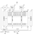
- FIG. 1 is a block diagram illustrating an exemplary configuration of an imaging device according to a first embodiment of the present technology.
- 1 is a block diagram showing an example of configuration of a solid-state imaging device according to a first embodiment of the present technology. It is a block diagram showing an example of 1 composition of a pixel in a 1st embodiment of this art. It is a block diagram showing an example of 1 composition of ADC (Analog to Digital Converter) in a 1st embodiment of this art. It is a figure showing an example of the connection form between pixels in a 1st embodiment of this art. It is a circuit diagram showing an example of 1 composition of a comparison circuit in a 1st embodiment of this art.
- ADC Analog to Digital Converter
- First embodiment example of extracting feature quantities that represent pixel signal differences by multiple values
- Second embodiment example of extracting a feature amount representing a difference between pixel signals by multiple values using a counter
- Third embodiment an example of holding a plurality of LBPs and extracting feature quantities representing pixel signal differences by multiple values from those LBPs
- Fourth embodiment example of extracting the feature amount by delaying the comparison result of the pixel of interest
- Fifth embodiment example of delaying comparison results of neighboring pixels to extract feature quantities
- FIG. 1 is a block diagram showing an exemplary configuration of an imaging device 100 according to a first embodiment of the present technology.
- the imaging apparatus 100 captures image data, and includes an optical unit 110, a solid-state imaging device 200, a digital signal processor 120, a display unit 130, an operation unit 140, a bus 150, a frame memory 160, a recording unit 170, and a power supply unit 180.
- a digital camera such as a digital still camera or a digital video camera, or an electronic device having an imaging function such as a cellular phone is assumed.
- the optical unit 110 captures incident light (image light) from a subject and forms an image on the imaging surface of the solid-state imaging device 200.
- the solid-state imaging device 200 picks up image data.
- the solid-state imaging device 200 captures image data in synchronization with a vertical synchronization signal VSYNC of a predetermined frequency (for example, 30 Hz), and supplies the image data to the digital signal processor 120 through a signal line 209.
- a vertical synchronization signal VSYNC of a predetermined frequency (for example, 30 Hz)
- the enable signal LBP_EN is input to the solid-state imaging device 200 through the signal line 208.
- the enable signal LBP_EN is a signal indicating whether to enable the function of extracting a feature and generating a feature image.
- the enable signal LBP_EN is set to enable
- the solid-state imaging device 200 generates a feature amount image and outputs the image data to the digital signal processor 120.
- the enable signal LBP_EN is set to be disabled, the solid-state imaging device 200 generates a normal image composed of pixel data according to the amount of received light, and outputs the image data to the digital signal processor 120.
- feature extraction mode the state of the imaging device 100 when the enable signal LBP_EN is enabled
- imaging mode the state of the imaging device 100 when the enable signal LBP_EN is disabled
- the digital signal processor 120 performs predetermined signal processing on image data.
- the digital signal processor 120 causes the frame memory 160 to hold image data as needed in signal processing.
- the digital signal processor 120 sets the enable signal LBP_EN based on the type of signal processing to be performed. For example, when performing image recognition, the digital signal processor 120 sets the enable signal LBP_EN to enable.
- the digital signal processor 120 sets the enable signal LBP_EN to disable.
- the digital signal processor 120 supplies the enable signal LBP_EN to the solid-state imaging device 200 via the signal line 208.
- the display unit 130 displays image data.
- a liquid crystal panel or an organic EL (Electro Luminescence) panel is used as the display unit 130.
- the operation unit 140 issues operation commands for various functions of the imaging apparatus 100 according to the operation by the user.
- the bus 150 is a common path for the solid-state imaging device 200, the digital signal processor 120, the display unit 130, the operation unit 140, the frame memory 160, the recording unit 170, and the power supply unit 180 to exchange information with each other.
- the frame memory 160 temporarily holds image data.
- the recording unit 170 records image data.
- a recording medium such as a hard disk or a semiconductor memory is used.
- the power supply unit 180 supplies power to each unit in the imaging device 100.
- FIG. 2 is a block diagram showing a configuration example of the solid-state imaging device 200 according to the first embodiment of the present technology.
- the solid-state imaging device 200 includes a DAC (Digital to Analog Converter) 211, a plurality of time code generation units 212, a vertical drive circuit 213, and a pixel array unit 220.
- the solid-state imaging device 200 further includes a pixel drive circuit 214, a timing generation circuit 215, and an output unit 250. These circuits are provided on a single semiconductor substrate.
- DAC Digital to Analog Converter
- the DAC 211 generates a reference signal by DA (Digital to Analog) conversion and supplies the reference signal to the pixel array unit 220.
- a reference signal for example, a ramp signal whose level monotonously decreases with the passage of time is used.
- the DAC 211 is an example of a reference signal supply unit described in the claims.
- the pixel array unit 220 further includes a plurality of pixels 230 arranged in a two-dimensional grid and a plurality of time code transfer units 221.
- a set of pixels 230 arranged in a predetermined direction horizontal direction or the like
- a set of pixels 230 arranged in a direction perpendicular to the row will be referred to as a “column”.
- the timing generation circuit 215 controls the operation timing of the DAC 211, the vertical drive circuit 213 and the pixel drive circuit 214 in synchronization with the vertical synchronization signal VSYNC.
- the timing generation circuit 215 is constituted by, for example, a timing generator.
- the enable signal LBP_EN is input to the timing generation circuit 215. When the enable signal LBP_EN is enabled, the timing generation circuit 215 controls the offset voltage of the reference signal by the control signal to the DAC 211.
- the time code generation unit 212 generates a time code indicating relative time within the cycle of the vertical synchronization signal VSYNC.
- the time code generation unit 212 is disposed for each time code transfer unit 221, and supplies the generated time code to the corresponding time code transfer unit 221.
- the time code transfer unit 221 transfers a time code.
- the pixel drive circuit 214 drives the pixels 230 in a predetermined order to generate an analog pixel signal.
- the vertical drive circuit 213 drives the pixels 230 in a predetermined order to convert pixel signals into digital signals and output them.
- the pixel 230 generates an analog pixel signal according to the amount of light received. Then, the pixel 230 converts the pixel signal into a digital signal, and supplies the digital signal to the output unit 250 through the time code transfer unit 221.
- the present invention is not limited to this configuration.
- the circuits can be distributed and arranged on a plurality of stacked semiconductor substrates.
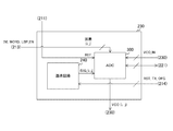
- FIG. 3 is a block diagram showing a configuration example of the pixel 230 according to the first embodiment of the present technology.
- the pixel 230 includes a pixel circuit 240 and an ADC 300.
- the pixel circuit 240 generates an analog signal according to the amount of received light as a pixel signal SIG_ (i, j) according to the control of the pixel drive circuit 214.
- i is an integer indicating the vertical coordinate of the pixel 230
- j is an integer indicating the horizontal coordinate.
- the pixel circuit 240 supplies the pixel signal SIG_ (i, j) to the ADC 300.
- the ADC 300 converts the pixel signal SIG_ (i, j) into a digital signal according to the control of the vertical drive circuit 213.
- the ADC 300 compares the reference signal REF from the DAC 211 with the pixel signal SIG_ (i, j), and generates a digital signal based on the comparison result VCO_ (i, j). Then, the ADC 300 supplies the generated digital signal to the time code transfer unit 221.
- the ADC 300 outputs the comparison result VCO_ (i, j) to the pixel 230 in the vicinity (hereinafter, referred to as “nearby pixel”). Further, VCO_IN, which is the comparison result of the adjacent pixels, is input to the ADC 300.
- “nearby” means that the Euclidean distance from the coordinates of a certain pixel to the coordinates of the other pixels is within a certain distance.
- a pixel whose Euclidean distance from the focused pixel of interest is less than “2” is set as a neighboring pixel.
- the neighboring pixels are eight pixels above and below, left and right, upper left, upper right, lower left and lower right of the pixel of interest.
- the pixel at coordinate (i, j) has coordinates (i-1, j-1), (i-1, j), (i-1, j + 1), (i, j-1), (i,
- the comparison result VCO_ (i, j) is output to the neighboring pixels of j + 1), (i + 1, j-1), (i + 1, j) and (i + 1, j + 1).
- 8-bit VCO_IN which is the comparison result of eight neighboring pixels, is input.
- the number of neighboring pixels is not limited to eight, and, for example, four pixels in the upper, lower, left, and right directions may be considered as neighboring pixels.
- the pixel circuit 240 of the pixel of interest is an example of the pixel circuit of interest described in the claims
- the pixel circuit 240 of the neighboring pixels is an example of the pixel circuit of claims described in the claims.
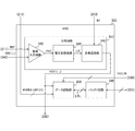
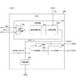
- FIG. 4 is a block diagram showing one configuration example of the ADC 300 according to the first embodiment of the present technology.
- the ADC 300 includes a comparison circuit 310, a data storage unit 350, and a buffer circuit 360.
- the comparison circuit 310 includes a differential input circuit 320, a voltage conversion circuit 330 and a positive feedback circuit 340.
- the circuit including the comparison circuits 310 of all the pixels is an example of the comparison unit described in the claims.
- the differential input circuit 320 compares the reference signal REF from the DAC 211 with the pixel signal SIG_ (i, j) from the pixel circuit 240.
- the differential input circuit 320 outputs a predetermined differential output signal HVO to the voltage conversion circuit 330 when the pixel signal SIG_ (i, j) is higher than the reference signal REF.
- the voltage conversion circuit 330 converts the voltage of the differential output signal HVO into a low potential at which the positive feedback circuit 340 can operate, and supplies it to the positive feedback circuit 340 as a conversion signal LVI.
- the positive feedback circuit 340 Inverts the comparison result VCO_ (i, j) to be inverted when the pixel signal SIG_ (i, j) is higher than the reference signal REF. And output. Also, the positive feedback circuit 340 is initialized by the initialization signal INI from the vertical drive circuit 213.
- the data storage unit 350 generates and stores LBP_ (i, j) based on the comparison result VCO_ (i, j) and VCO_IN when the enable signal LBP_EN is enabled. On the other hand, when the enable signal LBP_EN is disabled, the data storage unit 350 stores a time code when the comparison result VCO_ (i, j) is inverted as pixel data. The data storage unit 350 supplies those digital signals (LBP_ (i, j) or pixel data) to the buffer circuit 360 via the local bit line LBL.
- the data storage unit 350 is an example of a storage unit described in the claims.
- the buffer circuit 360 transfers a time code from the time code transfer unit 221 to the data storage unit 350, and transfers LBP_ (i, j) or pixel data from the data storage unit 350 to the time code transfer unit 221.
- the buffer circuit 360 is disposed in the pixel 230, this circuit can also be disposed in the time code transfer unit 221.
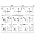
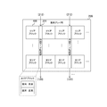
- FIG. 5 is a diagram illustrating an example of a connection form between pixels according to the first embodiment of the present technology.
- a pixel surrounded by a thick frame is set as a target pixel, and its coordinates are set as (i, j). Also, for example, coordinates (i-1, j-1), (i-1, j), (i-1, j + 1), (i, j-1), (i, j + 1), (i + 1, j- 1) Let eight pixels of (i + 1, j) and (i + 1, j + 1) be neighboring pixels.
- the target pixel is connected to each of the eight neighboring pixels through eight input signal lines.
- the 8-bit comparison result VCO_IN is input to the pixel of interest via the input signal lines. Further, the pixel of interest is connected to each of the neighboring pixels through one output signal line branched into eight.
- the target pixel outputs the 1-bit comparison result VCO_ (i, j) to each of the neighboring pixels through the output signal line.
- FIG. 6 is a circuit diagram showing one configuration example of the comparison circuit 310 in the first embodiment of the present technology.
- the differential input circuit 320 in the comparison circuit 310 includes pMOS (p-channel Metal-Oxide-Semiconductor) transistors 321 to 323 and nMOS (n-channel MOS) transistors 324 to 326.
- pMOS p-channel Metal-Oxide-Semiconductor
- nMOS n-channel MOS
- the pMOS transistors 321 and 322 form a current mirror circuit.
- the power supply voltage VDD1 is applied to the sources of the pMOS transistors 321, 322 and 323.
- the drain of the pMOS transistor 321 is commonly connected to the gates of the pMOS transistors 321 and 322 and the drain of the nMOS transistor 324.
- the drain of the pMOS transistor 322 is commonly connected to the drain of the nMOS transistor 325 and the gate of the pMOS transistor 323. Let the potential at this connection point be VO.
- the drain of the pMOS transistor 323 is connected to the voltage conversion circuit 330.
- the nMOS transistors 324 and 325 form a differential pair, and the sources of these transistors are commonly connected to the drain of the nMOS transistor 326.
- the source of the nMOS transistor 326 is connected to a predetermined reference potential VSS. Further, the reference signal REF from the DAC 211 is input to the gate of the nMOS transistor 324, and the pixel signal SIG_ (i, j) from the pixel circuit 240 is input to the gate of the nMOS transistor 325.
- a predetermined bias voltage Vb is applied to the gate of the nMOS transistor 326, and a predetermined reference potential VSS is applied to the source of the nMOS transistor 326.
- the voltage conversion circuit 330 includes an nMOS transistor 331.
- a predetermined bias voltage VBIAS is applied to the gate of the nMOS transistor 331.
- the drain of the nMOS transistor 331 is connected to the drain of the pMOS transistor 323, and the source is connected to the positive feedback circuit 340.
- the bias voltage VBIAS may be any value that can convert the transistor in the positive feedback circuit 340 operating at a constant voltage into a voltage that does not destroy the transistor.
- the bias voltage VBIAS can be the same as the power supply voltage of the positive feedback circuit 340.
- Positive feedback circuit 340 includes pMOS transistors 341, 342 and 343, and nMOS transistors 344 and 345.
- the pMOS transistors 341 and 342 and the nMOS transistor 344 are connected in series to the power supply voltage VDD2.
- the pMOS transistor 342 and the nMOS transistor 345 are connected in series to the power supply voltage VDD2.
- the magnitude relationship between the reference potential VSS and the power supply voltages VDD1 and VDD2 is expressed by the following equation. Note that, as described above, the bias voltage VBIAS is set to, for example, the same value as the power supply voltage VDD2. VSS ⁇ VDD2 ⁇ VDD1
- the initialization signal INI from the vertical drive circuit 213 is input to the gates of the pMOS transistor 341 and the nMOS transistor 344.
- the gate of the pMOS transistor 343 is connected to the connection point of the pMOS transistor 342 and the nMOS transistor 345.
- the gates of the pMOS transistor 342 and the nMOS transistor 345 are commonly connected to the voltage conversion circuit 330 and the connection node of the pMOS transistor 343 and the nMOS transistor 344.
- the potential at the connection point of the pMOS transistor 342 and the nMOS transistor 345 is output to the data storage unit 350 or the like as the comparison result VCO_ (i, j).
- the differential input circuit 320, the voltage conversion circuit 330, and the positive feedback circuit 340 are not limited to the circuits illustrated in FIG. 6 as long as they have the functions described with reference to FIG.
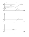
- FIG. 7 is a timing chart showing an example of the operation of the comparison circuit 310 in the first embodiment of the present technology.
- a in the same figure is a timing chart which shows an example of operation of differential input circuit 320 in comparison circuit 310.
- B in the figure is a timing chart showing an example of the operation of the voltage conversion circuit 330.
- C in the figure is a timing chart showing an example of the operation of the positive feedback circuit 340.
- the vertical axis in the figure is voltage, and the horizontal axis is time.
- the reference signal REF is set to a voltage higher than the pixel signals SIG of all the pixels 230 by the DAC 211, and the comparison circuit 310 is initialized by the high level initialization signal INI.
- the reference signal REF is input to one of the gates of the nMOS transistors 324 and 325 of the differential pair, and the pixel signal SIG_ (i, j) is input to the other gate.
- the voltage of the reference signal REF is higher than the voltage of the pixel signal SIG_ (i, j).
- most of the current output from the nMOS transistor 326 of the current source flows to the diode-connected pMOS transistor 321 via the nMOS transistor 324 on the reference signal REF side.
- the positive feedback circuit 340 as a charging circuit does not charge the conversion signal LVI.
- the high level initialization signal INI is supplied, the nMOS transistor 344 on the reference potential VSS side is turned on, and the positive feedback circuit 340 discharges the conversion signal LVI.
- the pMOS transistor 341 on the power supply side is shut off, the positive feedback circuit 340 does not charge the conversion signal LVI via the pMOS transistor 343. As a result, the conversion signal LVI is discharged to the reference potential VSS.
- the positive feedback circuit 340 outputs the comparison result VCO_ (i, j) at a high level by the pMOS transistor 342 and the nMOS transistor 345 of the output stage constituting the inverter, and the comparison circuit 310 is initialized.
- the vertical drive circuit 213 sets the initialization signal INI to the low level.
- the sweep of the reference signal REF is started after the timing Ts.
- the pMOS transistor 323 is turned off and is shut off, and the comparison result VCO is a high level signal, so the pMOS transistor 343 is turned off and shut off Be done.
- the nMOS transistor 344 is also cut off because the initialization signal INI is at low level.
- the conversion signal LVI maintains the reference potential VSS in the high impedance state, and a high level comparison result VCO is output.
- the output current of the nMOS transistor 326 of the current source does not flow in the nMOS transistor 324 on the reference signal REF side.
- the gate potentials of the pMOS transistors 321 and 322 constituting the current mirror circuit rise, and the channel resistance of the pMOS transistor 322 becomes high.
- the gate potential of the pMOS transistor 323 is lowered by the voltage drop caused by the current flowing through the nMOS transistor 325 on the pixel side, and the nMOS transistor 331 in the voltage conversion circuit 330 is conducted.
- the differential output signal HVO output from the pMOS transistor 323 is converted into a conversion signal LVI by the nMOS transistor 331 in the voltage conversion circuit 330, and is supplied to the positive feedback circuit 340.
- the positive feedback circuit 340 as a charging circuit charges the conversion signal LVI and gradually raises the potential from the reference potential VSS to the power supply voltage VDD2.
- the positive feedback circuit 340 rapidly charges the conversion signal LVI via the pMOS transistor 342 and the nMOS transistor 345, and raises the potential to the power supply voltage VDD2 at a stretch.
- the nMOS transistor 331 shuts off if the voltage of the conversion signal LVI reaches a voltage value lower than the bias voltage VBIAS by the threshold of the transistor. Even if the pMOS transistor 323 remains conductive, the conversion signal LVI is not charged more than that, and the voltage conversion circuit 330 also functions as a voltage clamp circuit.
- the charging of the conversion signal LVI due to the conduction of the pMOS transistor 343 is a positive feedback operation that accelerates its movement, starting from the fact that the conversion signal LVI has risen to the threshold of the inverter.
- the current source nMOS transistor 326 in the differential input circuit 320 is set to a very small current per circuit because the number of circuits simultaneously operating in parallel in the solid-state imaging device 200 is huge.
- the reference signal REF is swept very slowly because the voltage changing in unit time when the time code switches is the LSB (Least Significant Bit) step of AD conversion. Therefore, the change of the gate potential of the pMOS transistor 323 is also slow, and the change of the output current of the pMOS transistor 323 driven thereby is also slow.
- the comparison result VCO can make a transition quickly enough.
- the transition time of the comparison result VCO is a fraction of the unit time of the time code, and is typically 1 nanosecond (ns) or less.
- this output transition time can be achieved only by setting a small current of, for example, 0.1 microampere ( ⁇ A) in the nMOS transistor 326 of the current source.
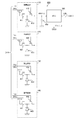
- FIG. 8 is a circuit diagram showing a configuration example of the pixel circuit 240 in the first embodiment of the present technology.
- the pixel circuit 240 includes a reset transistor 241, a transfer transistor 242, a floating diffusion layer 243, a photodiode 244, and a discharge transistor 245.
- a reset transistor 241 for example, an nMOS transistor is used as the reset transistor 241, the transfer transistor 242, the photodiode 244 and the discharge transistor 245.
- the photodiode 244 photoelectrically converts incident light to generate charge.
- the discharge transistor 245 discharges the charge of the photodiode 244 in accordance with the discharge control signal OFG from the pixel drive circuit 214.
- the transfer transistor 242 transfers charge from the photodiode 244 to the floating diffusion layer 243 in accordance with the transfer signal TX from the pixel drive circuit 214.
- the floating diffusion layer 243 stores the transferred charge, and generates a voltage according to the amount of the stored charge. A signal of this voltage is output to the differential input circuit 320 as a pixel signal SIG_ (i, j).
- the reset transistor 241 initializes the charge amount of the floating diffusion layer 243 in accordance with a reset signal RST from the pixel drive circuit 214.
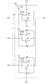
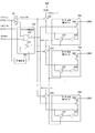
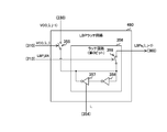
- FIG. 9 is a circuit diagram showing one configuration example of the data storage unit 350 in the first embodiment of the present technology.
- the data storage unit 350 includes a multiplexer 351, a latch control circuit 352, a plurality of switches 355, and a plurality of latch circuits 356.
- the switch 355 and the latch circuit 356 are provided for each neighboring pixel. When there are eight neighboring pixels, eight switches 355 and eight latch circuits 356 are provided.
- the multiplexer 351 switches the output destination of the comparison result VCO_ (i, j) according to the enable signal LBP_EN.
- the multiplexer 351 outputs the comparison result VCO_ (i, j) to all the switches 355 when the enable signal LBP_EN is enabled.
- the multiplexer 351 outputs the comparison result VCO_ (i, j) to the latch control circuit 352.
- the latch control circuit 352 controls each operation of the latch circuit 356.
- the latch control circuit 352 includes an OR (logical sum) gate 353 and an inverter 354.
- the OR gate 353 calculates the logical sum of the WORD signal for controlling the read timing of the pixel data and the comparison result VCO_ (i, j).
- the WORD signal is supplied from the vertical drive circuit 213.
- the OR gate 353 supplies the signal of the logical sum to all the latch circuits 356 as the control signal T.
- the inverter 354 inverts the comparison result VCO_ (i, j).
- the inverter 354 supplies the inverted signal as a control signal L to all the latch circuits 356.
- the switch 355 inputs the comparison result VCO from the corresponding neighboring pixel to the corresponding latch circuit 356 during a period until the comparison result VCO_ (i, j) from the multiplexer 351 is inverted.
- the latch circuit 356 holds one bit of data.
- the latch circuit 356 includes inverters 357 and 358 and a switch 359.
- the nth (n is an integer of 0 to 7) latch circuit 356 holds the nth bit of the time code.
- the nth bit of the local bit pattern is held in the nth latch circuit 356.
- the inverter 357 inverts the signal from the inverter 358 and outputs it to the input terminal of the inverter 358 and the switch 359 when the control signal L is at high level.
- the inverter 358 inverts one of the comparison result VCO of the corresponding neighboring pixels, the signal from the inverter 357, and the signal from the switch 359, and outputs the result to the input terminal of the inverter 357.
- These looped inverters 357 and 358 hold (latch) a 1-bit signal.
- Switch 359 switches the path between buffer circuit 360 and the loop circuit formed of inverters 357 and 358 in accordance with control signal T.
- control signal T When the control signal T is high, the switch 359 is controlled to be in the closed state, and when it is low, it is controlled to be in the open state.
- the latch control circuit 352 latches eight time codes updated at each unit time from the time code transfer unit 221 while the high level comparison result VCO_ (i, j) is input in the write operation. It is stored in the circuit 356. Then, when the reference signal REF and the pixel signal SIG_ (i, j) become the same voltage and the comparison result VCO is inverted to the low level, the latch control circuit 352 stops the writing (updating) of the time code. The latch control circuit 352 causes the latch circuit 356 to hold the time code finally stored in the latch circuit 356.
- the time code stored in eight latch circuits 356 represents the time when the pixel signal SIG_ (i, j) and the reference signal REF become equal, and the pixel signal SIG_ (i, j) is the reference of that time. It represents pixel data indicating that it is a voltage, that is, a digitized light quantity value.
- the latch control circuit 352 causes the time code transfer unit 221 to output the stored time code when the read timing comes, based on the WORD signal that controls the read timing.
- the time code transfer unit 221 sequentially transfers the supplied time code in the column direction (vertical direction), and supplies the time code to the output unit 250.
- VCO_IN when the comparison result VCO_ (i, j) is inverted is written to the eight latch circuits 356.
- the written data corresponds to LBP. Then, this LBP is read according to the WORD signal.
- the DAC 211 sequentially supplies a plurality of reference signals REF having different offset voltages, and the data storage unit 350 sequentially executes writing and reading of LBP each time the reference signal REF is supplied. For example, when four reference signals REF are supplied, writing and reading of LBP are performed four times each.
- the number of bits of pixel data and the number of bits of LBP are the same, the number of bits of these may be different.
- the same number of latch circuits 356 as the larger one of the number of bits of pixel data and the number of bits of LBP is provided, and the switches 355 of the number equal to or larger than the number of bits of LBP are provided.
- pixel data is 16 bits and LBP is 8 bits
- 16 latch circuits 356 and 8 or more switches 355 are provided.
- FIG. 10 is a circuit diagram showing an exemplary configuration of buffer circuit 360.
- the buffer circuit 360 includes a bidirectional buffer 361 for each latch circuit 356. In the case of eight latch circuits 356, eight bidirectional buffers 361 are provided.
- the bidirectional buffer 361 transfers data bidirectionally in accordance with the WR signal instructing writing and the RD signal instructing reading from the vertical drive circuit 213.
- the bidirectional buffer 361 includes a buffer 362 and an inverter 363.
- the buffer 362 outputs the nth bit of the time code to the data storage unit 350 via the local bit line LBL in accordance with the WR signal.
- the inverter 363 inverts the n-th bit of the digital signal (pixel data or LBL) from the data storage unit 350 according to the RD signal and supplies it to the time code transfer unit 221.
- FIG. 11 is a timing chart showing an example of the reset level sampling operation according to the first embodiment of the present technology. This operation is started when the enable signal LBP_EN is set to disable (that is, imaging mode) and imaging is instructed.
- the reference signal REF is set to the reset voltage Vrst from the standby voltage Vstb so far. Thereby, the floating diffusion layer 243 is reset.
- the initialization signal INI for the positive feedback circuit 340 is set to the high level, whereby the positive feedback circuit 340 is initialized.
- the reference signal REF is raised to a predetermined voltage Vu, and comparison of the reference signal REF with the pixel signal SIG_ (i, j) is started.
- the comparison result VCO_ (i, j) is at the high level because the reference signal REF is larger than the pixel signal SIG_ (i, j).
- the comparison result VCO_ (i, j) is inverted from the high level to the low level.
- the time code (that is, pixel data) at the time of the inversion is stored in the data storage unit 350.
- the voltage of the reference signal REF is lowered to the standby voltage Vstb to such an extent that the nMOS transistor 324 in the comparison circuit 310 is turned off.
- the current consumption of the comparison circuit 310 during the read period is suppressed.
- the WORD signal that controls the readout timing becomes high level, and for example, 8-bit pixel data is output from the data storage unit 350.
- the data acquired here is P phase data of a reset level when performing CDS (Correlated Double Sampling) processing.
- FIG. 12 is a timing chart illustrating an example of a signal level sampling operation according to the first embodiment of the present technology.
- the reference signal REF is raised to the predetermined voltage Vu, the initialization signal INI is set to the high level, and the positive feedback circuit 340 is initialized again.
- the charge generated by the photodiode 244 is transferred to the floating diffusion layer 243 by the high level transfer signal TX.
- comparison of the reference signal REF and the pixel signal SIG_ (i, j) is started. Then, at time t8 when the reference signal REF and the pixel signal SIG_ (i, j) become identical, the comparison result VCO_ (i, j) is inverted, and the time code (that is, the time code) is stored in the data storage unit 350. Pixel data is stored.
- the voltage of the reference signal REF is lowered to the standby voltage Vstb such that the nMOS transistor 324 in the comparison circuit 310 is turned off.
- the WORD signal that controls the readout timing becomes high level, and for example, 8-bit pixel data is output from the data storage unit 350.
- the data acquired here is D-phase data of signal level at the time of performing CDS processing.
- each pixel 230 in the solid-state imaging device 200 is capable of global shutter operation in which all pixels are simultaneously reset and all pixels are simultaneously exposed. Since all the pixels can be exposed and read out simultaneously, there is usually no need for a holding portion provided in the pixel for holding the electric charge until it is read out.
- a selection transistor or the like for selecting a pixel to be driven which is required in a column parallel readout type solid-state imaging device, is not necessary.
- FIG. 13 is a timing chart showing an example of the operation of the solid-state imaging device 200 at the time of latching the low level in the LBP extraction mode according to the first embodiment of the present technology. This operation is started when the enable signal LBP_EN is set to enable (ie, LBP extraction mode) and imaging is instructed.
- the vertical axis in the figure is voltage, and the horizontal axis is time.
- the DAC 211 sequentially supplies a plurality of reference signals REF having different offset voltages for each period of the vertical synchronization signal VSYNC.
- the offset voltage is a fixed voltage applied to the entire reference signal REF.
- the two reference signals REF having different offset voltages have the same slope slope, but have a difference in potential at a predetermined phase of the slope (for example, the sweep start time).
- the DAC 211 sequentially generates four reference signals in the cycle of the vertical synchronization signal VSYNC, and sets them as REFa, REFb, REFc, and REFd.
- the shape of these reference signals is assumed to be stepped.
- the offset voltage of the reference signal REFa is “0” (V)
- the offset voltage of the reference signal REFb is the negative voltage ofs1.
- the offset voltage of the reference signal REFc is a negative voltage ofs2 which is larger in absolute value than ofs1
- the offset voltage of the reference signal REFd is a negative voltage ofs3 which is larger in absolute value than ofs2.
- the DAC 211 supplies the reference signal REFa at time TL1 and supplies the reference signal REFb at time TL2. Then, the DAC 211 supplies the reference signal REFc at time TL3 and supplies the reference signal REFd at time TL4.
- the pixel drive circuit 214 outputs a pixel signal to each pixel by the transfer signal TX.
- the potential of the pixel signal SIG_ (i, j) of the pixel of interest is equal to or less than the potential of the pixel signal SIG_ (i-1, j-1) of the neighboring pixel at the upper left.
- the comparison result VCO_ (i-1, j-1) of the neighboring pixels is inverted at time T12 and becomes low level, and after that time, for example, the comparison result VCO_ (i, j) of the target pixel at time T13. Is reversed.
- the switch 355 is closed until time T13 when the comparison result VCO_ (i, j) of the target pixel is inverted, and the comparison result VCO_ (i-1, j-1) is written to the corresponding latch circuit 356.
- This bit is, for example, a latch L7.
- the latch L7 corresponds to a bit corresponding to a neighboring pixel in LBP.
- the latch circuit 356 holds the low level latch L7. Ru. As described above, when the potential of the pixel signal of the pixel of interest is equal to or less than that of the nearby pixel, the corresponding latch circuit 356 holds a low level bit.
- the charge to be stored is electrons
- the larger the amount of light received by the pixel the larger the amount of stored electrons, and the lower the potential of the pixel signal. Therefore, when the pixel value of the pixel of interest is equal to or greater than that of a nearby pixel, a low level bit is held in the corresponding latch circuit 356.
- FIG. 14 is a timing chart showing an example of the operation of the solid-state imaging device 200 at the time of latching a high level in the LBP extraction mode according to the first embodiment of the present technology.
- the vertical axis in the figure is voltage, and the horizontal axis is time.
- the potential of the pixel signal SIG_ (i, j) of the pixel of interest is higher than the pixel signal SIG_ (i + 1, j + 1) of the neighboring pixel at the lower right.
- the comparison result VCO_ (i, j) of the target pixel is first inverted at time T12 and becomes low level, and then the comparison result VCO_ (i + 1, j + 1) of the neighboring pixels is inverted at time T13.
- the switch 355 is closed until time T12 when the comparison result VCO_ (i, j) of the target pixel is inverted, and the comparison result VCO_ (i + 1, j + 1) is written to the corresponding latch circuit 356.
- This bit is, for example, a latch L3.
- the latch circuit 356 holds the high level latch L3.
- the corresponding latch circuit 356 holds a high level bit. That is, when the pixel value of the pixel of interest is smaller than that of the neighboring pixels, the corresponding latch circuit 356 holds a high level bit.
- FIG. 15 is a diagram for describing LBP in the first embodiment of the present technology.
- a in the same figure is a figure which shows the pixel value of an analog pixel signal for every pixel.
- B in the same figure is a figure which represented the magnitude correlation of each pixel signal of a vicinity pixel and an attention pixel by 2 values.
- the data storage unit 350 of the pixel of interest holds the LBP value of low level when the pixel value of the pixel of interest is equal to or greater than that of the neighboring pixel, and holds the bit of high level otherwise. For example, since the pixel values of the neighboring pixels at the upper left, upper and lower, and right positions of the pixel of interest are less than or equal to the pixel of interest, "0" bits are retained for these pixels. The “1” bit is held for neighboring pixels other than those.
- the target pixel arranges the held 8 bits clockwise, for example, from the bit corresponding to the left neighboring pixel and outputs the result.
- the feature quantity representing the comparison result of the pixel values of the neighboring pixel and the target pixel in binary notation is called LBP.
- noise reduction by CDS processing performed in the imaging mode can not be performed in principle, so it is effective to reduce noise by a method not using CDS processing.
- a method can be applied in which the pulse of the reset signal RST to the reset transistor 241 is transitioned to a low level more slowly than in the imaging mode when the pixel drive circuit 214 performs a reset.
- a method of band limitation can be applied by inserting a low pass filter or the like.
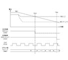
- FIG. 16 is a diagram illustrating an example of LBP for each reference signal in the first embodiment of the present technology.
- the DAC 211 sequentially supplies four reference signals with different offset voltages to all the pixels.
- the vertical axis in the figure is voltage, and the horizontal axis is time.
- a solid line indicates the pixel signal of the pixel of interest, and a dotted line indicates the pixel signal of a nearby pixel.
- the DAC 211 supplies a reference signal REFb to which a negative offset voltage is added.
- This offset voltage changes the timing at which the comparison result VCO is inverted for each pixel. For example, when the potential of the pixel signal of the target pixel becomes lower than the reference signal REFb at time TL6, the comparison result VCO_ (i, j) of the target pixel is inverted. At this time TL6, the potentials of the three neighboring pixels are higher than the reference signal REFb, and the LBP value of “0” is held for those neighboring pixels. As a result, “00011111” is generated as LBPb_ (i, j).
- the DAC 211 supplies a reference signal REFc to which an offset voltage having a larger absolute value than the reference signal REFb is added.
- This offset voltage changes the timing at which the comparison result VCO is inverted for each pixel. For example, when the potential of the pixel signal of the target pixel becomes lower than the reference signal REFc at time TL7, the comparison result VCO_ (i, j) of the target pixel is inverted. At this time TL7, the potentials of the four neighboring pixels are higher than that of the reference signal REFb, and the LBP value of “0” is held for those neighboring pixels. As a result, “00001111” is generated as LBPc_ (i, j).
- the DAC 211 supplies a reference signal REFd to which an offset voltage having a larger absolute value than the reference signal REFc is added.
- This offset voltage changes the timing at which the comparison result VCO is inverted for each pixel. For example, when the potential of the pixel signal of the target pixel becomes lower than the reference signal REFd at time TL8, the comparison result VCO_ (i, j) of the target pixel is inverted. At this time TL8, the potentials of the five neighboring pixels are higher than that of the reference signal REFb, and the LBP value of “0” is held for those neighboring pixels. As a result, “00000111” is generated as LBPd_ (i, j).
- the timing at which the comparison result VCO_ (i, j) of the target pixel is inverted that is, the timing at which the comparison result VCO of the neighboring pixels is latched changes. Due to the change of the timing, the comparison result VCO is likely to change in the neighboring pixels where the potential difference with the target pixel is small. For example, the neighboring pixels at coordinates (i + 1, j + 1) have the smallest potential difference with the target pixel. In this neighboring pixel, the comparison result VCO_ (i + 1, j + 1) is at the low level at time TL5, but the comparison result VCO_ (i + 1, j + 1) changes to the high level at time TL6.
- the comparison result VCO hardly changes even if the offset voltage is changed.
- the neighboring pixels at coordinates (i-1, j-1) have the largest potential difference with the target pixel.
- the comparison result VCO_ (i ⁇ 1, j ⁇ 1) remains at the high level at the times TL5 to TL8.
- the comparison result VCO does not change regardless of the potential difference.
- the potential of the neighboring pixel at the coordinate (i + 1, j) is equal to or higher than the potential of the pixel of interest.
- the comparison result VCO_ (i + 1, j) remains at the low level at times TL5 to TL8.
- the number of “1” bits in the corresponding bits LBPa to LBPd increases as the potential difference with the target pixel increases.
- the DAC 211 supplies four reference signals having different offset voltages, the DAC 211 can supply other than four reference signals. Also, although the DAC 211 applies a negative offset voltage, it may apply a positive offset voltage. In this case, the magnitude of the potential difference can be represented by the number of “1” bits for neighboring pixels whose potential is equal to or higher than the pixel of interest. The DAC 211 can also sequentially supply a reference signal to which a negative offset voltage is added and a reference signal to which a positive offset voltage is added.
- FIG. 17 is a block diagram illustrating an exemplary configuration of the output unit 250 according to the first embodiment of the present technology.
- the output unit 250 includes a switch 251, a feature amount converter 252, a signal processor 253, and an output circuit 254.
- the switch 251 switches the output destination of data from the pixel array unit 220 according to the enable signal LBP_EN.
- the switch 251 When the enable signal LBP_EN is enabled, the switch 251 outputs LBPa_ (i, j) to LBPd_ (i, j) from the pixel array unit 220 to the feature amount conversion unit 252.
- the switch 251 when the enable signal LBP_EN is disabled, the switch 251 outputs the pixel data PIX_ (i, j) from the pixel array unit 220 to the signal processing unit 253.
- the feature amount conversion unit 252 converts LBPa_ (i, j) to LBPd_ (i, j) into a feature amount Fv_ (i, j) that represents the difference between the pixel signal and the pixel of interest for each neighboring pixel by multiple values. It is a thing.
- the feature amount conversion unit 252 counts the number of “1” for each digit of LBPa_ (i, j) to LBPd_ (i, j). Then, the feature amount conversion unit 252 outputs data in which those count values are arranged to the output circuit 254 as a feature amount Fv_ (i, j).
- the range of count values of the number of “1” s in a certain digit is “0” to “4”.
- the count value represents the magnitude of the potential difference.
- the signal processing unit 253 executes predetermined signal processing such as black level correction processing for correcting the black level and CDS processing on the pixel data PIX_ (i, j).
- predetermined signal processing such as black level correction processing for correcting the black level and CDS processing on the pixel data PIX_ (i, j).
- the signal processing unit 253 subtracts the D phase data from the P phase data, it is possible to cancel the variation of the comparison circuit 310, the charge injection of the reset operation, the feedthrough, and the like.
- the signal processing unit 253 supplies the pixel data after the signal processing to the output circuit 254.
- the output circuit 254 outputs the data from the feature amount conversion unit 252 or the signal processing unit 253 to the digital signal processor 120 according to the control of the timing generation circuit 215.
- the output unit 250 performs conversion to the feature amount Fv_ (i, j)
- a circuit in the subsequent stage such as the digital signal processor 120 in place of the output unit 250 has the feature amount Fv_ (i, j). It can also be configured to perform conversion to.
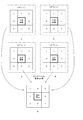
- FIG. 18 is a diagram for describing conversion processing by the feature amount conversion unit 252 in the first embodiment of the present technology.
- a indicates an example of LBPa_ (i, j)
- b in the figure indicates an example of LBPb_ (i, j).
- C in the same figure shows an example of LBPc_ (i, j)
- d in the same figure shows an example of LBPd_ (i, j).
- E in the same figure shows an example of feature-value Fv_ (i, j).
- the feature amount conversion unit 252 counts the number of “1” for each digit of LBPa_ (i, j) to LBPd_ (i, j). For example, the digits corresponding to the upper left neighboring pixel are all “1” in LBPa_ (i, j) to LBPd_ (i, j). Therefore, "4" is set to the digit corresponding to the upper left neighboring pixel of the feature amount Fv_ (i, j). The digits corresponding to the lower left neighboring pixel are all “0” in LBPa_ (i, j) to LBPd_ (i, j). Therefore, “0” is set to the digit corresponding to the lower left neighboring pixel of the feature amount Fv_ (i, j).
- the feature amount Fv_ (i, j) represents the difference between the pixel signal and the pixel of interest in multiple values for each neighboring pixel. Therefore, the amount of information of the feature amount Fv_ (i, j) is large, and the image quality of the feature amount image is improved, as compared with LBP in which the magnitude relationship of the pixel signal with the target pixel is represented by two values for each neighboring pixel. For this reason, the digital signal processor 120 performs image recognition using the feature amount image including the feature amount Fv_ (i, j), thereby improving the recognition accuracy as compared to the case where the feature amount image including LBP is used. It can be done.
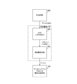
- FIG. 19 is a diagram summarizing the processing flow in the imaging device 100 according to the first embodiment of the present technology.
- the pixel circuit 240 generates an analog signal corresponding to the amount of received light as a pixel signal, and supplies the analog signal to the ADC 300.
- the ADC 300 generates LBPa_ (i, j) to LBPd_ (i, j) using four reference signals REF with different offset voltages, and supplies the LBPa_ (i, j) to the feature quantity conversion unit 252.
- the feature amount conversion unit 252 is a feature amount Fv_ (i, j) that represents LBPa_ (i, j) to LBPd_ (i, j) for each pixel and the difference between the pixel signal and the target pixel for each neighboring pixel by multiple values. And supply the digital signal processor 120. In other words, the feature amount Fv_ (i, j) is extracted for each pixel.
- the circuit including the ADC 300 and the feature amount conversion unit 252 is an example of the feature amount extraction unit described in the claims.
- the digital signal processor 120 performs an image recognition process or the like on the feature amount image formed of the feature amount Fv_ (i, j).
- a solid-state imaging device AD converts a pixel signal to generate a normal image
- an external processor extracts LBP from the normal image.
- the LBP is directly extracted from the pixel signal in the solid-state imaging device 200, not in the processor outside the solid-state imaging device 200. Therefore, it is not necessary to perform AD conversion of the pixel signal, and power consumption of the imaging device 100 can be reduced accordingly.
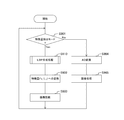
- FIG. 20 is a flowchart illustrating an example of the operation of the imaging device 100 according to the first embodiment of the present technology. This operation is started, for example, when a predetermined application for capturing image data is executed in the imaging device 100.
- the imaging apparatus 100 determines whether the feature amount extraction mode has been set (step S901). When the feature amount extraction mode is set (step S901: Yes), the imaging device 100 performs LBP generation processing for generating LBP (step S910). Then, the imaging apparatus 100 converts LBP into feature quantity Fv_ (i, j) for each pixel (step S902), and performs image recognition on the feature quantity image (step S903).
- step S901 When the feature amount extraction mode is not set (step S901: No), the imaging device 100 AD converts the pixel signal for each pixel to generate a normal image (step S904), and performs various operations on the normal image. Image processing is executed (step S905). After step S 903 or S 905, the imaging device 100 repeatedly executes step S 901 and subsequent steps.
- FIG. 21 is a flowchart illustrating an example of LBP generation processing according to the first embodiment of the present technology.
- the solid-state imaging device 200 in the imaging device 100 generates LBPa_ (i, j) for each pixel using the reference signal REFa (step S911). Then, the solid-state imaging device 200 changes the offset voltage of the reference signal (step S912), and generates LBPb_ (i, j) for each pixel using the changed reference signal REFb (step S913).
- the solid-state imaging device 200 changes the offset voltage of the reference signal (step S914), and generates LBPc_ (i, j) for each pixel using the changed reference signal REFc (step S915). Then, the solid-state imaging device 200 changes the offset voltage of the reference signal (step S916), and generates LBPd_ (i, j) for each pixel using the changed reference signal REFd (step S917). After step S917, the solid-state imaging device 200 ends the LBP generation process.
- the solid-state imaging device 200 extracts the feature amount Fv_ (i, j) that represents the difference between the pixel signals of the neighboring pixels and the pixel of interest in multiple values. Therefore, it is possible to increase the information amount of the feature amount as compared with LBP which expresses the difference by two values. Thereby, the image quality of the feature amount image can be improved, and the recognition accuracy of the image recognition can be enhanced.
- the solid-state imaging device 200 extracts the feature amount Fv_ (i, j) using a plurality of reference signals generated in order, but the ADC 300 is more likely to be used as the number of reference signals increases. Conversion time will be longer. When the conversion time becomes long, the time for which the pixel circuit 240 holds the analog pixel signal SIG_ (i, j) becomes long, and there is a high possibility that the signal level may fluctuate due to the influence of the leak current or the like. As a result, the accuracy of AD conversion is reduced. In order to shorten the AD conversion time, only one reference signal may be used and AD conversion may be performed using a counter. The solid-state imaging device 200 of the second embodiment is different from that of the first embodiment in that AD conversion is performed using a counter.
- FIG. 22 is a block diagram illustrating a configuration example of the ADC 300 according to the second embodiment of the present technology.
- the ADC 300 of the second embodiment differs from that of the first embodiment in that a counting unit 370 is provided instead of the data storage unit 350.
- the counting unit 370 includes a counting circuit 371 for each neighboring pixel.
- the counting circuit 371 counts the count value over the period between the time when the comparison result VCO_ (i, j) of the target pixel is inverted and the time when the comparison result VCO of the corresponding neighboring pixels is inverted. .
- the counting unit 370 outputs data consisting of these count values to the buffer circuit 360 via the local bit line LBL as the feature amount Fv_ (i, j).
- the feature amount conversion unit 252 is not provided in the output unit 250 of the second embodiment.
- FIG. 23 is a circuit diagram showing one configuration example of the counting circuit 371 in the second embodiment of the present technology.
- the counting circuit 371 includes a NAND (negative logical product) gate 372, a NOR (negative logical sum) gate 373 and an up / down counter 380.
- the NAND gate 372 uses the negative logical product of the comparison result (VCO_ (i, j-1) or the like) of the corresponding neighboring pixels and the comparison result VCO_ (i, j) of the target pixel as the start flag STA. Output.
- the start flag STA is set to the high level when the comparison result of any of the pixel of interest and the corresponding neighboring pixel is inverted by the NAND operation, and the counting of the up / down counter 380 is started.
- the NOR gate 373 outputs the NOR of the comparison result of the corresponding neighboring pixels and the comparison result VCO_ (i, j) of the target pixel to the up / down counter 380 as the stop flag STP.
- the stop flag STP is set to the high level when the comparison result of both the target pixel and the corresponding neighboring pixel is inverted by the NOR operation, and the counting of the up / down counter 380 ends.
- the up / down counter 380 counts the count value of the code according to the comparison result of the corresponding neighboring pixels.
- the comparison result of the corresponding neighboring pixels is input to the up / down counter 380 as the up / down flag UD. Further, the clock signal CLK from the vertical drive circuit 213 is input to the up / down counter 380.
- the up / down counter 380 increments (that is, up counts) the count value in synchronization with the clock signal CLK if the up / down flag UD is high. On the other hand, if the up / down flag UD is at low level, the up / down counter 380 decrements (that is, down counts) the count value in synchronization with the clock signal CLK.
- the stop flag STP goes high, the up / down counter 380 stops counting. Then, the up / down counter 380 outputs the count value to the buffer circuit 360.
- the count value is a multi-value and is represented by a bit string of 2 bits or more.
- the number of bits may be smaller than the number of bits (eg, 10 bits or more) of pixel data in the imaging mode. For example, when the range of the count value is in the range of “ ⁇ 3” to “+3”, 3 bits including 1 bit indicating the sign and 2 bits indicating the absolute value are output as the count value.
- the frequency of the clock signal CLK in the LBP extraction mode may be lower than the frequency of the clock signal in the imaging mode.
- the imaging mode is set to several tens to several hundreds of megahertz (MHz)
- the LBP extraction mode is set to several kilohertz (kHz) to several tens of hertz (Hz).
- FIG. 24 is a circuit diagram showing one configuration example of the up / down counter 380 in the second embodiment of the present technology.
- the up / down counter 380 includes an inverter 381, a NAND gate 382, a NOR gate 383 and a JK flip flop 384.
- the up / down counter 380 also includes XOR (exclusive OR) gates 385 and 387, JK flip flops 386 and 389, and an AND (logical product) gate 388.
- the inverter 381 inverts the up / down flag UD.
- the inverter 381 supplies the inverted signal to the XOR gates 385 and 387.
- the NAND gate 382 outputs the negative logical product of the clock signal CLK and the start flag STA to the NOR gate 383.
- the NOR gate 383 outputs the NOR of the signal from the NAND gate 382 and the stop flag STP to the JK flip flops 384, 386 and 389.
- the JK flip flop 384 holds the zeroth bit of the count value. A high level is input to the input terminals J and K of the JK flip flop 384, and the inverted value of the signal from the NOR gate 383 is input to the clock terminal. Further, the JK flip flop 384 outputs the held value to the XOR gate 385 and the buffer circuit 360 from the output terminal Q.
- the XOR gate 385 outputs an exclusive OR of the signal from the inverter 381 and the signal from the flip flop 384 to the JK flip flop 386 and the AND gate 388.
- the JK flip flop 386 holds the first bit of the count value.
- the signal from the XOR gate 385 is input to the input terminals J and K of the JK flip flop 386, and the inverted value of the signal from the NOR gate 383 is input to the clock terminal. Further, the JK flip flop 386 outputs the held value to the XOR gate 387 and the buffer circuit 360 from the output terminal Q.
- the XOR gate 387 outputs an exclusive OR of the signal from the inverter 381 and the signal from the flip flop 386 to the AND gate 388.
- the AND gate 388 outputs the logical product of the signals from each of the XOR gates 385 and 387 to the JK flip flop 389.
- the JK flip flop 389 holds the second bit of the count value.
- the signal from the AND gate 388 is input to the input terminals J and K of the JK flip flop 389, and the inverted value of the signal from the NOR gate 383 is input to the clock terminal.
- the JK flip flop 389 outputs the held value to the buffer circuit 360.
- the circuit in the up / down counter 380 is not limited to the configuration illustrated in FIG. 24 as long as the function described in FIG. 23 can be realized.
- FIG. 25 is a timing chart illustrating an example of an operation of performing up-counting according to the second embodiment of the present technology. As illustrated in the figure, the DAC 211 of the second embodiment supplies the sloped reference signal REF only once.
- the potential of the pixel signal SIG_ (i-1, j-1) of the neighboring pixel at the coordinate (i-1, j-1) is higher than the potential of the pixel signal SIG_ (i, j) of the target pixel.
- the comparison result VCO_ (i-1, j-1) of the neighboring pixels is first inverted at time T51, and then the comparison result VCO_ (i, j) of the target pixel is inverted at time T52.
- the up / down counter 380 counts up from time T51 to time T52, and acquires, for example, a count value of “+1”.
- a count value As described above, when the potential of the pixel signal of the nearby pixel is higher than the potential of the pixel signal of the target pixel, the up-counting is performed. Then, the larger the potential difference between the target pixel and the neighboring pixels, the longer the counting period and the larger the count value. Therefore, the count value indicates the magnitude of the potential difference between the pixel signals of the pixel of interest and the neighboring pixels.
- FIG. 26 is a timing chart illustrating an example of an operation of performing down-counting according to the second embodiment of the present technology.
- the potential of the pixel signal SIG_ (i + 1, j + 1) of the neighboring pixel at the coordinate (i + 1, j + 1) is lower than the potential of the pixel signal SIG_ (i, j) of the target pixel.
- the comparison result VCO_ (i, j) of the target pixel is inverted first at time T53, and then the comparison result VCO_ (i + 1, j + 1) of the target pixel is inverted at time T54.
- the up / down counter 380 counts down from time T53 to time T54, and acquires, for example, a count value of “ ⁇ 3”. As described above, when the potential of the pixel signal of the nearby pixel is lower than the potential of the pixel signal of the target pixel, down-counting is performed.
- the sign of the count value indicates which of the pixel signal of the target pixel and the pixel signal of the neighboring pixel is larger. When the values of these pixel signals substantially match, the count value is “0”.
- the DAC 211 does not have to supply a plurality of reference signals. Therefore, the conversion time of the ADC 300 can be shortened as compared with the first embodiment.
- FIG. 27 is a diagram summarizing the processing flow in the imaging device 100 according to the second embodiment of the present technology.
- the pixel circuit 240 generates an analog signal corresponding to the amount of received light as a pixel signal as in the first embodiment, and supplies the analog signal to the ADC 300.
- the ADC 300 counts the count value based on the comparison result of the pixel signal and the reference signal, and extracts the feature value Fv_ (i, j) similar to that of the first embodiment for each pixel.
- the ADC 300 is an example of the feature quantity extraction unit described in the claims.
- the digital signal processor 120 performs an image recognition process or the like on the feature amount image formed of the feature amount Fv_ (i, j).
- the feature amount Fv_ (i, j) differs from LBP which indicates only the magnitude relationship between the pixel signal of the pixel of interest and the neighboring pixels, and indicates the magnitude of the difference between those pixel signals. Therefore, by using the feature amount Fv_ (i, j), is the difference between the pixel signals sufficiently buried in various noises such as kTC noise and the offset of the comparison circuit 310, or a significant value It can be determined whether it was. Therefore, the recognition accuracy of image recognition can be improved.
- the ADC 300 sequentially supplies a plurality of reference signals in order to extract the feature amount by counting the count value based on the comparison result of the pixel signal and the reference signal.
- the conversion time of the ADC 300 can be shortened compared to the first embodiment. Thereby, the accuracy of AD conversion can be improved.
- the ADC 300 performs LBP writing and reading each time a reference signal is supplied, but the number of readings increases as the number of reference signals increases. Resulting in. If the number of readings increases, the conversion time of the ADC 300 may be increased, and the accuracy of AD conversion may be reduced.
- the solid-state imaging device 200 of the third embodiment is different from that of the first embodiment in that the number of times of data readout is reduced by reading out a plurality of data collectively.
- FIG. 28 is a block diagram showing a configuration example of the ADC 300 according to the third embodiment of the present technology.
- the ADC 300 of the third embodiment is different from the first embodiment in that a plurality of data storage units 350 are provided.
- the number of data storage units 350 is, for example, the same as the number (4) of reference signals. Further, the number of buffer circuits 360 is the same as that of the data storage unit 350.
- the vertical drive circuit 213 supplies the enable signal LBPa_EN to the data storage unit 350 corresponding to the reference signal REFa when the reference signal REFa is supplied.
- the data storage unit 350 holds LBPa.
- the vertical drive circuit 213 supplies the enable signal LBPb_EN to the data storage unit 350 corresponding to the reference signal REFb when the reference signal REFb is supplied.
- the data storage unit 350 holds LBPb.
- the vertical drive circuit 213 sequentially supplies the enable signals LBPc_EN and LBPd_EN, and the corresponding data storage unit 350 holds LBPc and LBPd.
- the vertical drive circuit 213 When LBP is held in all the data storage units 350, the vertical drive circuit 213 supplies a WORD signal to all the data storage units 350 to execute the read operation of LBPa to LBPd. Thus, when the data storage unit 350 holds all of LBPa to LBPd, the vertical drive circuit 213 can read those data collectively.
- the solid-state imaging device 200 writes the plurality of LBPs in the plurality of data storage units 350 after reading out all the LBPs.
- the conversion time of the ADC 300 can be shortened.
- the accuracy of AD conversion can be improved without using the up / down counter 380.
- the solid-state imaging device 200 holds the high level bit when the potential of the pixel signal is higher than that of the neighboring pixel.
- a high level bit may be held even when the relationship is not satisfied. For example, when the potential difference between the pixel signal of the pixel of interest and the neighboring pixels is less than a predetermined value, it is determined that the potential difference is generated due to noise, and the pixel 230 holds a high level bit if the potential difference is larger than a predetermined value. , Can reduce the effects of noise.
- the ADC 300 according to the fourth embodiment is different from the first embodiment in that the pixel 230 holds a high level bit when the potential difference is larger than a predetermined value.
- FIG. 29 is a circuit diagram showing a configuration example of a data storage unit 350 in the fourth embodiment of the present technology.
- the data storage unit 350 of the fourth embodiment is different from the first embodiment in that a delay circuit 390 is further provided.
- the delay circuit 390 delays the comparison result VCO_ (i, j) of the pixel of interest over a predetermined delay time dT.
- the delay circuit 390 supplies the delayed comparison result VCO_ (i, j) to the latch control circuit 352.
- the amount of fluctuation of the reference signal during the delay time dT is fixed, and when the amount of fluctuation is dV fix , a high level bit is held when the potential difference between the pixel signals of the pixel of interest and the neighboring pixels is larger than dV fix. Be done.
- the delay circuit 390 delays the comparison result VCO_ (i, j) of the pixel of interest, the pixel of interest is more than the fixed value dV fix according to the delay time.
- the potential difference between the adjacent pixels is large, "1" can be reliably held. This can reduce the influence of noise.
- the ADC 300 holds the bit at the high level when the potential of the pixel signal is higher than that of the neighboring pixels.
- a high level bit may be held even when the relationship is not satisfied. For example, when the potential difference between the pixel signal of the pixel of interest and the neighboring pixels is less than a predetermined value, it is determined that the potential difference is generated due to noise, and the pixel 230 holds a high level bit if the potential difference is larger than a predetermined value. , Can reduce the effects of noise.
- the ADC 300 according to the fifth embodiment is different from the ADC 300 according to the first embodiment in which the pixel 230 holds a high level bit when the potential difference is larger than a predetermined value.
- FIG. 30 is a block diagram showing a configuration example of the ADC 300 according to the fifth embodiment of the present technology.
- the ADC 300 of the fifth embodiment is different from the first embodiment in that a delay circuit 390 is further provided.
- the delay circuit 390 delays the comparison result VCO of adjacent pixels for a predetermined delay time dT.
- the delay circuit 390 supplies the delayed comparison result VCO to the respective data storage units 350 of the neighboring pixels.
- the delay circuit 390 delays the comparison result VCO of the neighboring pixels, the potential difference between the pixel of interest and the neighboring pixels than the fixed value dV fix according to the delay time. Is large, it is possible to hold "1" reliably. This makes it possible to reduce the influence of noise without delaying the comparison result VCO_ (i, j) of the pixel of interest.
- the ADC 300 is disposed for each pixel in the pixel array unit 220.
- the circuit scale per pixel may increase. For example, if a floating diffusion layer or a transistor is shared by a plurality of pixels, the circuit scale per pixel can be reduced.
- the pixel array unit 220 of the sixth embodiment is different from that of the first embodiment in that a plurality of pixels share a floating diffusion layer.
- FIG. 31 is a plan view showing a configuration example of the pixel array unit 220 according to the sixth embodiment of the present technology.
- a plurality of area blocks 400 are arranged in a two-dimensional grid.
- a plurality of pixels are arranged.
- four pixels are arranged in two rows and two columns.
- the pixels in the area block 400 share the floating diffusion layer and the ADC 300.
- FIG. 32 is a circuit diagram showing a configuration example of the area block 400 in the sixth embodiment of the present technology.
- the area block 400 includes pixel circuits 410, 420, 430 and 440, a floating diffusion layer 450, and an ADC 300.
- the pixel circuit 410 includes a discharge transistor 411, a transfer transistor 412, and a photodiode 413.
- the pixel circuit 420 includes a discharge transistor 421, a transfer transistor 422, and a photodiode 423.
- the pixel circuit 430 includes a discharge transistor 431, a transfer transistor 432 and a photodiode 433.
- the pixel circuit 440 includes a discharge transistor 441, a transfer transistor 442 and a photodiode 443.
- the photodiode 413 photoelectrically converts incident light to generate charge.
- the discharge transistor 411 discharges the charge of the photodiode 413 according to the discharge control signal OFG.
- the transfer transistor 412 transfers charge from the photodiode 413 to the floating diffusion layer 450 in accordance with the transfer signal TX0.
- transfer signals TX1, TX2, and TX3 are supplied to the pixel circuits 420, 430, and 440.
- the pixel drive circuit 214 sequentially supplies the transfer signals TX0, TX1, TX2, and TX3 to transfer charges in order.
- the number of shared pixels is not limited to four.
- eight pixels may share the floating diffusion layer 450 or the like.
- a circuit per pixel is compared with a configuration in which the floating diffusion layer 450 and the like are arranged for each pixel. Can be reduced in size.
- the solid-state imaging device 200 performs the exposure for each image when capturing both the normal image and the feature amount image. That is, at least two exposures had to be performed. However, when one of the normal image and the feature amount image is generated and held by exposure, if the other is also generated and held subsequently, it is not necessary to perform the exposure again.
- the solid-state imaging device 200 according to the seventh embodiment is different from the first embodiment in that both a normal image and a feature amount image are generated by one exposure.
- FIG. 33 is a circuit diagram showing one configuration example of the data storage unit 350 in the seventh embodiment of the present technology.
- the data storage unit 350 of the seventh embodiment includes a latch control circuit 352, a plurality of LBP latch circuits 460, and a plurality of time code latch circuits 470.
- the LBP latch circuit 460 is arranged for each neighboring pixel. Further, the number of time code latch circuits 470 is the same as the number of bits of the time code. For example, in the case where the neighboring pixels are eight pixels and the time code is eight bits, eight LBP latch circuits 460 and eight time code latch circuits 470 are respectively arranged.
- the LBP latch circuit 460 holds the comparison result VCO of the corresponding neighboring pixels according to the control of the latch control circuit 352.
- Time code latch circuit 470 holds corresponding bits of the time code under the control of latch control circuit 352.
- FIG. 34 is a circuit diagram showing a configuration example of the LBP latch circuit 460 in the seventh embodiment of the present technology.
- the LBP latch circuit 460 includes a switch 355 and a latch circuit 356. These functions are the same as the circuit of the same name in the first embodiment.
- FIG. 35 is a circuit diagram showing a configuration example of the time code latch circuit 470 according to the seventh embodiment of the present technology.
- the time code latch circuit 470 includes inverters 461 and 462 and a switch 463.
- the inverter 461 inverts the signal from the inverter 462 according to the control signal L, and outputs the inverted signal to the input terminal of the inverter 462 and the switch 463.
- the inverter 462 inverts the signal from the switch 463 or the inverter 461 and outputs the inverted signal to the input terminal of the inverter 461.
- the switch 463 opens and closes the path between the loop circuit formed of the inverters 461 and 462 and the buffer circuit 360 according to the control signal T.
- the vertical drive circuit 213 causes the eight LBP latch circuits 460 to hold LBP at the end of exposure, and then causes the eight time code latch circuits 470 to hold time codes as pixel data. Then, the vertical drive circuit 213 sequentially outputs LBPa to LBPd and a normal image composed of pixel data.
- the data storage unit 350 since the data storage unit 350 further holds the time code in addition to LBP, it is possible to generate both the feature image and the normal image by one exposure. it can.
- the pixel of interest in the pixel array unit 220 outputs the comparison result VCO_ (i, j) to all eight neighboring pixels. It is desirable to reduce the number of wires because the number of wires for transmitting data increases. However, in order to reduce the number of wires, it is necessary to perform processing to restore LBP whose number of bits has decreased due to the reduction in the number of wires to the original number of bits.
- the solid-state imaging device 200 according to the eighth embodiment is different from the first embodiment in that the number of wirings for transmitting the comparison result is reduced and the LBP is restored.
- FIG. 36 is a diagram for describing wiring connection of signal lines in the eighth embodiment of the present technology.
- a in the same figure is a figure which shows the connection relation of the attention pixel in a 1st embodiment, and a neighboring pixel.
- B in the same figure is a figure which shows the connection relation of the attention pixel in a 8th embodiment, and a neighboring pixel.
- thick arrows represent the wiring of the neighboring pixels connected to the latch of the pixel of interest
- thin solid arrows represent the wiring connected to the latches of the neighboring pixels.
- the direction of the arrow indicates the connection direction.
- the first embodiment there are a plurality of sets of arrows overlapping in directions opposite to each other. This indicates that the relative relationship between the pixel value of the pixel of interest and the pixel values of the neighboring pixels is acquired redundantly.
- the LBP values obtained by the pixels linked by a pair of overlapping arrows facing in opposite directions are equivalent as information (the size relation of two pixels), and the LBP value itself is the other bit inversion value. is there.
- the wiring connection between neighboring pixels can be reduced to half.
- one of the pair of neighboring pixels in a point-symmetrical position with respect to the target pixel is connected to the target pixel.
- the upper left neighboring pixel and the lower right neighboring pixel of the target pixel are point symmetrical with respect to the target pixel, the upper left neighboring pixel is connected and the lower right neighboring pixel is not connected.
- the number of LBP bits acquired in each pixel is half (for example, 4 bits), a desired LBP can be completely restored by arithmetic processing described later.
- FIG. 37 is a circuit diagram showing a configuration example of a data storage unit 350 in the eighth embodiment of the present technology.
- the number of switches 355 and latch circuits 356 is reduced to half (for example, four) as compared with the first embodiment.
- FIG. 38 is a circuit diagram showing a configuration example of the output unit 250 in the eighth embodiment of the present technology.
- the output unit 250 of the eighth embodiment differs from that of the first embodiment in that the output processing unit 250 further includes an interpolation processing unit 255.
- the interpolation processing unit 255 interpolates a bit corresponding to the other in LBP composed of bits corresponding to one of a pair of neighboring pixels in a position symmetrical with respect to the pixel of interest.
- the interpolation processing unit 255 performs interpolation, for example, by the following processing.
- the 0th bit of the LBP value obtained for the target pixel is used as it is as the 0th bit of the target pixel.
- the first bit of the LBP value obtained for the target pixel is also used as the first bit of the target pixel.
- the second bit of the LBP value obtained for the target pixel is used directly as the second bit value of the target pixel, and the third bit of the LBP value obtained for the target pixel is directly used as the third bit value of the target pixel.
- the 0th bit of the LBP value obtained at the neighboring pixel at the coordinate (i + 1, j + 1) is inverted to obtain the value of the 4th bit of the target pixel.
- the first bit of the LBP value obtained at the neighboring pixel at the coordinate (i + 1, j) is inverted to obtain the value of the fifth bit of the target pixel.
- the second bit of the LBP value obtained in the neighboring pixel is inverted to (i-1, j + 1) of the target pixel to obtain the sixth bit value of the target pixel.
- the third bit of the LBP value obtained at the neighboring pixel of the coordinate (i, j-1) is inverted to obtain the value of the seventh bit of the target pixel.
- the imaging device 100 performs the interpolation processing in the solid-state imaging device 200
- the interpolation processing may be performed outside the solid-state imaging device 200 (such as the digital signal processor 120).
- the connection is made with all the neighboring pixels.
- the number of wirings of the pixel array unit 220 can be reduced compared to the case of FIG.
- the circuit scale of the data storage unit 350 can be reduced.
- the technology according to the present disclosure can be applied to various products.
- the technology according to the present disclosure is realized as a device mounted on any type of mobile object such as a car, an electric car, a hybrid electric car, a motorcycle, a bicycle, personal mobility, an airplane, a drone, a ship, a robot May be
- FIG. 39 is a block diagram showing a schematic configuration example of a vehicle control system that is an example of a mobile control system to which the technology according to the present disclosure can be applied.
- Vehicle control system 12000 includes a plurality of electronic control units connected via communication network 12001.
- the vehicle control system 12000 includes a drive system control unit 12010, a body system control unit 12020, an external information detection unit 12030, an in-vehicle information detection unit 12040, and an integrated control unit 12050.
- a microcomputer 12051, an audio image output unit 12052, and an in-vehicle network I / F (interface) 12053 are illustrated as a functional configuration of the integrated control unit 12050.
- the driveline control unit 12010 controls the operation of devices related to the driveline of the vehicle according to various programs.
- the drive system control unit 12010 includes a drive force generation device for generating a drive force of a vehicle such as an internal combustion engine or a drive motor, a drive force transmission mechanism for transmitting the drive force to the wheels, and a steering angle of the vehicle. adjusting steering mechanism, and functions as a control device of the braking device or the like to generate a braking force of the vehicle.
- Body system control unit 12020 controls the operation of the camera settings device to the vehicle body in accordance with various programs.
- the body system control unit 12020 functions as a keyless entry system, a smart key system, a power window device, or a control device of various lamps such as a headlamp, a back lamp, a brake lamp, a blinker or a fog lamp.
- the body system control unit 12020 the signal of the radio wave or various switches is transmitted from wireless controller to replace the key can be entered.
- Body system control unit 12020 receives an input of these radio or signal, the door lock device for a vehicle, the power window device, controls the lamp.
- Outside vehicle information detection unit 12030 detects information outside the vehicle equipped with vehicle control system 12000.
- an imaging unit 12031 is connected to the external information detection unit 12030.
- the out-of-vehicle information detection unit 12030 causes the imaging unit 12031 to capture an image outside the vehicle, and receives the captured image.
- the external information detection unit 12030 may perform object detection processing or distance detection processing of a person, a vehicle, an obstacle, a sign, characters on a road surface, or the like based on the received image.
- Imaging unit 12031 receives light, an optical sensor for outputting an electric signal corresponding to the received light amount of the light.
- the imaging unit 12031 can output an electric signal as an image or can output it as distance measurement information.
- the light image pickup unit 12031 is received may be a visible light, it may be invisible light such as infrared rays.
- Vehicle information detection unit 12040 detects the vehicle information.
- a driver state detection unit 12041 that detects a state of a driver is connected to the in-vehicle information detection unit 12040.
- the driver state detection unit 12041 includes, for example, a camera for imaging the driver, and the in-vehicle information detection unit 12040 determines the degree of fatigue or concentration of the driver based on the detection information input from the driver state detection unit 12041. It may be calculated or it may be determined whether the driver does not go to sleep.
- the microcomputer 12051 calculates a control target value of the driving force generation device, the steering mechanism or the braking device based on the information inside and outside the vehicle acquired by the outside information detecting unit 12030 or the in-vehicle information detecting unit 12040, and a drive system control unit A control command can be output to 12010.
- the microcomputer 12051 is collision avoidance or cushioning of the vehicle, follow-up running based on inter-vehicle distance, vehicle speed maintained running, functions realized in the vehicle collision warning, or ADAS including lane departure warning of the vehicle (Advanced Driver Assistance System) It is possible to perform coordinated control aiming at
- the microcomputer 12051 the driving force generating device on the basis of the information around the vehicle acquired by the outside information detection unit 12030 or vehicle information detection unit 12040, by controlling the steering mechanism or braking device, the driver automatic operation such that autonomously traveling without depending on the operation can be carried out cooperative control for the purpose of.
- the microcomputer 12051 can output a control command to the body system control unit 12020 based on the information outside the vehicle acquired by the external information detection unit 12030.
- the microcomputer 12051 controls the headlamps in response to the preceding vehicle or the position where the oncoming vehicle is detected outside the vehicle information detection unit 12030, the cooperative control for the purpose of achieving the anti-glare such as switching the high beam to the low beam It can be carried out.
- Audio and image output unit 12052 transmits, to the passenger or outside of the vehicle, at least one of the output signal of the voice and image to be output device to inform a visually or aurally information.
- an audio speaker 12061, a display unit 12062, and an instrument panel 12063 are illustrated as the output device.
- Display unit 12062 may include at least one of the on-board display and head-up display.
- FIG. 40 is a diagram illustrating an example of the installation position of the imaging unit 12031.
- imaging units 12101, 12102, 12103, 12104, and 12105 are provided as the imaging unit 12031.
- the imaging units 12101, 12102, 12103, 12104, and 12105 are provided, for example, at positions such as the front nose of the vehicle 12100, a side mirror, a rear bumper, a back door, and an upper portion of a windshield of a vehicle interior.
- the imaging unit 12101 provided in the front nose and the imaging unit 12105 provided in the upper part of the windshield in the vehicle cabin mainly acquire an image in front of the vehicle 12100.
- the imaging units 12102 and 12103 included in the side mirror mainly acquire an image of the side of the vehicle 12100.
- the imaging unit 12104 provided in the rear bumper or the back door mainly acquires an image of the rear of the vehicle 12100.
- the imaging unit 12105 provided on the top of the windshield in the passenger compartment is mainly used to detect a leading vehicle or a pedestrian, an obstacle, a traffic light, a traffic sign, a lane, or the like.
- FIG. 40 illustrates an example of the imaging range of the imaging units 12101 to 12104.
- Imaging range 12111 indicates an imaging range of the imaging unit 12101 provided in the front nose
- imaging range 12112,12113 are each an imaging range of the imaging unit 12102,12103 provided on the side mirror
- an imaging range 12114 is The imaging range of the imaging part 12104 provided in the rear bumper or the back door is shown. For example, by overlaying the image data captured by the imaging units 12101 to 12104, a bird's eye view of the vehicle 12100 viewed from above can be obtained.
- At least one of the imaging unit 12101 through 12104 may have a function of obtaining distance information.
- at least one of the imaging units 12101 to 12104 may be a stereo camera including a plurality of imaging devices, or an imaging device having pixels for phase difference detection.
- the microcomputer 12051 based on the distance information obtained from to no imaging unit 12101 12104, and the distance to the three-dimensional object in to no imaging range 12111 in 12114, the temporal change of the distance (relative speed with respect to the vehicle 12100) In particular, it is possible to extract a three-dimensional object traveling at a predetermined speed (for example, 0 km / h or more) in substantially the same direction as the vehicle 12100 as a leading vehicle, in particular by finding the it can. Further, the microcomputer 12051 can set an inter-vehicle distance to be secured in advance before the preceding vehicle, and can perform automatic brake control (including follow-up stop control), automatic acceleration control (including follow-up start control), and the like. Automatic operation or the like for autonomously traveling without depending on the way of the driver operation can perform cooperative control for the purpose.
- automatic brake control including follow-up stop control
- automatic acceleration control including follow-up start control
- the microcomputer 12051 converts three-dimensional object data relating to three-dimensional objects into two-dimensional vehicles such as two-wheeled vehicles, ordinary vehicles, large vehicles, classification and extracted, can be used for automatic avoidance of obstacles.
- the microcomputer 12051 identifies obstacles around the vehicle 12100 into obstacles visible to the driver of the vehicle 12100 and obstacles difficult to see.
- the microcomputer 12051 determines a collision risk which indicates the risk of collision with the obstacle, when a situation that might collide with the collision risk set value or more, through an audio speaker 12061, a display portion 12062 By outputting a warning to the driver or performing forcible deceleration or avoidance steering via the drive system control unit 12010, driving support for collision avoidance can be performed.
- At least one of the imaging unit 12101 to 12104 may be an infrared camera that detects infrared rays.
- the microcomputer 12051 can recognize a pedestrian by determining whether a pedestrian is present in the images captured by the imaging units 12101 to 12104.
- Such pedestrian recognition is, for example, a procedure for extracting feature points in images captured by the imaging units 12101 to 12104 as an infrared camera, and pattern matching processing on a series of feature points indicating the outline of an object to determine whether it is a pedestrian or not
- the procedure is to determine Microcomputer 12051 is, determines that the pedestrian in the captured image of the imaging unit 12101 to 12104 is present, recognizing the pedestrian, the sound image output unit 12052 is rectangular outline for enhancement to the recognized pedestrian to superimpose, controls the display unit 12062.
- the audio image output unit 12052 is, an icon or the like indicating a pedestrian may control the display unit 12062 to display the desired position.
- the example of the vehicle control system to which the technology according to the present disclosure can be applied has been described above.
- the technology according to the present disclosure may be applied to, for example, the imaging unit 12031 among the configurations described above.
- the imaging device 100 described in FIG. 1 can be applied to the imaging unit 12031.
- the processing procedure described in the above embodiment may be regarded as a method having a series of these procedures, and a program for causing a computer to execute the series of procedures or a recording medium storing the program. You may catch it.
- a recording medium for example, a CD (Compact Disc), an MD (Mini Disc), a DVD (Digital Versatile Disc), a memory card, a Blu-ray disc (Blu-ray (registered trademark) Disc) or the like can be used.
- the present technology can also be configured as follows.
- a plurality of pixel circuits each of which generates an analog signal according to the amount of light received and outputs it as a pixel signal, Among the plurality of pixel circuits, a feature value representing the magnitude of the difference between the pixel signal from the neighboring pixel circuit in the vicinity of the focused pixel circuit of interest and each focused pixel circuit by multiple values for each neighboring pixel circuit
- An imaging apparatus comprising a feature quantity extraction unit to be extracted.
- the feature quantity extraction unit A comparison unit that compares the pixel signal with each of the plurality of reference signals and outputs the comparison result; A storage unit that sequentially generates and stores a plurality of local bit patterns based on the comparison result;
- the image pickup apparatus according to (2) further including: a feature amount conversion unit configured to convert data including the plurality of local bit patterns into the feature amount.
- the storage unit includes a plurality of data storage units that generate and store different local bit patterns.
- the image pickup apparatus according to (3), wherein the feature amount conversion unit reads each of the local bit patterns after the local bit pattern is stored in all of the plurality of data storage units, and converts it into the feature amount.
- the imaging device according to (3) or (4), wherein the storage unit further stores a time code indicating a time when the comparison result is inverted.
- the comparison unit outputs the comparison result of the pixel signal from the target pixel circuit and each of the plurality of reference signals as a target pixel comparison result and the pixel signal from the neighboring pixel circuit Outputting the comparison result with each of a plurality of reference signals as a neighboring pixel comparison result;
- the data storage unit is A latch circuit that holds the neighboring pixel comparison result; A latch control circuit for holding the neighboring pixel comparison result in the latch circuit when the target pixel comparison result is inverted;
- the delay circuit according to any one of (3) to (5), including: a delay circuit that delays one of the target pixel comparison result and the neighboring pixel comparison result for a predetermined time and outputs the result to either the latch circuit or the latch control circuit.
- the imaging device according to any of the above. (7) The imaging device according to (6), wherein the delay circuit delays the target pixel comparison result and outputs the result to the latch control circuit. (8) The imaging device according to (6), wherein the delay circuit delays the neighboring pixel comparison result and outputs the result to the latch circuit.
- the feature quantity extraction unit A comparison unit that compares each of the pixel signals with a predetermined reference signal and outputs the result as a comparison result; Counting a count value over a period between the time when the comparison result corresponding to the pixel circuit of interest is inverted and the time when the comparison result corresponding to the neighboring pixel circuit is inverted, and output as the feature quantity
- the imaging apparatus according to (1) comprising: (10) The counting unit increments the count value when one of the comparison result corresponding to the target pixel circuit and the comparison result corresponding to the neighboring pixel circuit is inverted earlier than the other.
- the imaging device according to (9), wherein the count value is decremented when the other is reversed earlier than the one.
- the plurality of pixel circuits are disposed in each of a plurality of area blocks, Each of the plurality of area blocks is The imaging device according to any one of (1) to (10), including the plurality of pixel circuits and a floating diffusion layer supplied by the plurality of pixel circuits.
- the near pixel circuit includes a pair of near pixel circuits in a point symmetrical position with respect to the target pixel circuit,
- the feature quantity extraction unit extracts the feature quantity representing the magnitude of the difference between the pixel signals from one of the pair of neighboring pixel circuits and the target pixel circuit from each of the plurality of (1)
- the imaging device in any one of 11).
- the imaging apparatus according to any one of (1) to (12), further including an image processing unit that performs processing of recognizing a predetermined object based on the feature amount.
- a feature value representing the magnitude of the difference between the pixel signal from the neighboring pixel circuit in the vicinity of the focused pixel circuit of interest and each focused pixel circuit by multiple values for each neighboring pixel circuit A control method of an imaging device comprising a feature quantity extraction procedure to be extracted.
- Reference Signs List 100 image pickup apparatus 110 optical unit 120 digital signal processor 130 display unit 140 operation unit 150 bus 160 frame memory 170 recording unit 180 power supply unit 200 solid-state imaging device 211 DAC 212 time code generation unit 213 vertical drive circuit 214 pixel drive circuit 215 timing generation circuit 220 pixel array unit 221 time code transfer unit 230 pixel 240, 410, 420, 430, 440 pixel circuit 241 reset transistor 242, 412, 422, 432, 442 transfer transistor 243, 450 floating diffusion layer 244, 413, 423, 433, 443 photodiode 245, 411, 421, 431, 441 discharge transistor 250 output part 251, 355, 359, 463 switch 252 feature amount conversion part 253 signal processing Block 254 Output circuit 255 Interpolation processor 300 ADC 310 comparison circuit 320 differential input circuit 321, 322, 323, 341, 342, 343 pMOS transistor 324, 325, 326, 331, 344, 345 nMOS transistor 330 voltage conversion circuit 340 positive feedback circuit 350 data storage unit
Landscapes
- Engineering & Computer Science (AREA)
- Multimedia (AREA)
- Signal Processing (AREA)
- Transforming Light Signals Into Electric Signals (AREA)
Abstract
特徴量画像を撮像する撮像装置において、特徴量画像の画質を向上させる。 撮像装置は、複数の画素回路と、特徴量抽出部とを具備する。この撮像装置において複数の画素回路のそれぞれは、受光量に応じたアナログ信号を生成して画素信号として出力する。また、撮像装置において特徴量抽出部は、複数の画素回路のうち注目した注目画素回路の近傍の近傍画素回路と注目画素回路とのそれぞれからの画素信号の差の大きさを近傍画素回路ごとに多値により表す特徴量を抽出する。
Description
本技術は、撮像装置、および、撮像装置の制御方法に関する。詳しくは、画像の特徴量を抽出する撮像装置、および、撮像装置の制御方法に関する。
従来より、画像認識、テクスチャ分割やリアルタイム動画解析などの画像処理を行うシステムなどにおいて、LBP(Local Binary Pattern)が用いられている。LBPは、注目画素の近傍の近傍画素毎に、その近傍画素と注目画素との画素値の大小関係を2値(1ビット)で表した特徴量である。このLBPは、画像全体の明るさの変化に対して頑健(ロバスト)であるという特性を有している。例えば、近傍画素を8画素として、画素ごとに8ビットのLBPを算出し、それらのLBPを二次元格子状に配列した画像を用いて画像認識を行う認識システムが提案されている(例えば、非特許文献1参照。)。以下、LBPなどの特徴量を二次元格子状に配列した画像を「特徴量画像」と称する。また、受光量に応じた値の画素データを二次元格子状に配列した一般的な画像を「通常画像」と称する。
Timo Ojala, et al., Multiresolution Gray-Scale and Rotation invariant Texture Classification with Local Binary Patterns, IEEE Transactions on Pattern Analysis and Machine Intelligence, vol.24, no.7, July 2002
上述の従来技術では、画像全体の明るさの変化に対して頑健なLBPからなる特徴量画像を用いて画像認識を行うため、その明るさの変化に起因する画像認識の認識結果の変動を抑制することができる。しかしながら、LBPからなる特徴量画像は、一般に通常画像と比較して画質が低いという問題がある。画質が低いと画像認識の精度が低下するため、特徴量画像の画質を向上することが望ましい。
本技術はこのような状況に鑑みて生み出されたものであり、特徴量画像を撮像する撮像装置において、特徴量画像の画質を向上させることを目的とする。
本技術は、上述の問題点を解消するためになされたものであり、その第1の側面は、それぞれが受光量に応じたアナログ信号を生成して画素信号として出力する複数の画素回路と、上記複数の画素回路のうち注目した注目画素回路の近傍の近傍画素回路と上記注目画素回路とのそれぞれからの上記画素信号の差の大きさを上記近傍画素回路ごとに多値により表す特徴量を抽出する特徴量抽出部とを具備する撮像装置、および、その制御方法である。これにより、近傍画素回路と注目画素回路とのそれぞれからの画素信号の差の大きさを近傍画素回路ごとに多値により表す特徴量が抽出されるという作用をもたらす。
また、この第1の側面において、オフセット電圧が互いに異なる複数の参照信号を順に供給する参照信号供給部をさらに具備し、上記特徴量抽出部は、上記画素信号と上記複数の参照信号のそれぞれとを比較した比較結果に基づいて上記特徴量を抽出することもできる。これにより、画素信号と複数の参照信号のそれぞれとを比較した比較結果から特徴量が抽出されるという作用をもたらす。
また、この第1の側面において、上記特徴量抽出部は、上記画素信号と上記複数の参照信号のそれぞれとを比較して上記比較結果を出力する比較部と、上記比較結果に基づいて複数のローカルビットパターンを順に生成して記憶する記憶部と、上記複数のローカルビットパターンからなるデータを上記特徴量に変換する特徴量変換部とを備えてもよい。これにより、複数のローカルビットパターンからなるデータが特徴量に変換されるという作用をもたらす。
また、この第1の側面において、上記記憶部は、互いに異なるローカルビットパターンを生成して記憶する複数のデータ記憶部を備え、上記特徴量変換部は、上記複数のデータ記憶部の全てに上記ローカルビットパターンが記憶された後に上記ローカルビットパターンのそれぞれを読み出して上記特徴量に変換することもできる。これにより、複数のデータ記憶部の全てにローカルビットパターンが記憶された後にローカルビットパターンのそれぞれが読み出されるという作用をもたらす。
また、この第1の側面において、上記記憶部は、上記比較結果が反転したときの時刻を示す時刻コードをさらに記憶することもできる。これにより、時刻コードから通常画像が生成されるという作用をもたらす。
また、この第1の側面において、上記比較部は、上記注目画素回路からの上記画素信号と上記複数の参照信号のそれぞれとの上記比較結果を注目画素比較結果として出力するとともに上記近傍画素回路からの上記画素信号と上記複数の参照信号のそれぞれとの上記比較結果を近傍画素比較結果として出力し、上記データ記憶部は、上記近傍画素比較結果を保持するラッチ回路と、上記注目画素比較結果が反転したときに上記近傍画素比較結果を上記ラッチ回路に保持させるラッチ制御回路と、上記注目画素比較結果および上記近傍画素比較結果の一方を所定時間に亘って遅延させて上記ラッチ回路および上記ラッチ制御回路のいずれかに出力する遅延回路とを備えてもよい。これにより、注目画素比較結果および近傍画素比較結果との一方が遅延するという作用をもたらす。
また、この第1の側面において、上記遅延回路は、上記注目画素比較結果を遅延させて上記ラッチ制御回路に出力することもできる。これにより、注目画素比較結果が遅延するという作用をもたらす。
また、この第1の側面において、上記遅延回路は、上記近傍画素比較結果を遅延させて上記ラッチ回路に出力することもできる。これにより、近傍画素比較結果が遅延するという作用をもたらす。
また、この第1の側面において、上記画素信号のそれぞれと所定の参照信号とを比較して比較結果として出力する比較部と、上記注目画素回路に対応する上記比較結果が反転する時刻と上記近傍画素回路に対応する上記比較結果が反転する時刻との間の期間に亘って計数値を計数して上記特徴量として出力する計数部とを具備することもできる。これにより、注目画素回路に対応する比較結果が反転する時刻と近傍画素回路に対応する比較結果が反転する時刻との間の期間に亘って計数値が計数されるという作用をもたらす。
また、この第1の側面において、上記計数部は、上記注目画素回路に対応する上記比較結果と上記近傍画素回路に対応する上記比較結果との一方が他方よりも先に反転した場合には上記計数値を増分し、上記他方が上記一方よりも先に反転した場合には上記計数値を減分することもできる。これにより、注目画素回路に対応する比較結果と近傍画素回路に対応する比較結果とのいずれが先に反転するかにより計数値が増分または減分されるという作用をもたらす。
また、この第1の側面において、上記複数の画素回路は、複数のエリアブロックのそれぞれに配置され、上記複数のエリアブロックのそれぞれは、上記複数の画素回路と上記複数の画素回路により供給される浮遊拡散層とを備えてもよい。これにより、浮遊拡散層を共有する複数の画素回路のそれぞれからの画素信号の差の大きさを表す特徴量が抽出されるという作用をもたらす。
また、この第1の側面において、上記近傍画素回路は、上記注目画素回路に対して点対称の位置の一対の近傍画素回路を含み、上記特徴量抽出部は、上記一対の近傍画素回路の一方と上記注目画素回路とのそれぞれからの上記画素信号の差の大きさを多値により表す上記特徴量を抽出することもできる。これにより、一対の近傍画素回路の一方と注目画素回路とのそれぞれからの画素信号の差の大きさを多値により表す上記特徴量が抽出されるという作用をもたらす。
また、この第1の側面において、上記特徴量に基づいて所定の物体を認識する処理を行う画像処理部をさらに具備してもよい。これにより、所定の物体が認識されるという作用をもたらす。
本技術によれば、特徴量画像を撮像する撮像装置において、特徴量画像の画質を向上させることができるという優れた効果を奏し得る。なお、ここに記載された効果は必ずしも限定されるものではなく、本開示中に記載されたいずれかの効果であってもよい。
以下、本技術を実施するための形態(以下、実施の形態と称する)について説明する。説明は以下の順序により行う。
1.第1の実施の形態(画素信号の差を多値により表す特徴量を抽出する例)
2.第2の実施の形態(画素信号の差を多値により表す特徴量を、カウンタを用いて抽出する例)
3.第3の実施の形態(複数のLBPを保持し、画素信号の差を多値により表す特徴量を、それらのLBPから抽出する例)
4.第4の実施の形態(注目画素の比較結果を遅延させて特徴量を抽出する例)
5.第5の実施の形態(近傍画素の比較結果を遅延させて特徴量を抽出する例)
6.第6の実施の形態(画素共有型の素子において、画素信号の差を多値により表す特徴量を抽出する例)
7.第7の実施の形態(時刻コードおよびLBPを保持し、画素信号の差を多値により表す特徴量をLBPから抽出し、時刻コードから通常画像を生成する例)
8.第8の実施の形態(配線数を削減した固体撮像素子において画素信号の差を多値により表す特徴量を抽出する例)
9.移動体への応用例
1.第1の実施の形態(画素信号の差を多値により表す特徴量を抽出する例)
2.第2の実施の形態(画素信号の差を多値により表す特徴量を、カウンタを用いて抽出する例)
3.第3の実施の形態(複数のLBPを保持し、画素信号の差を多値により表す特徴量を、それらのLBPから抽出する例)
4.第4の実施の形態(注目画素の比較結果を遅延させて特徴量を抽出する例)
5.第5の実施の形態(近傍画素の比較結果を遅延させて特徴量を抽出する例)
6.第6の実施の形態(画素共有型の素子において、画素信号の差を多値により表す特徴量を抽出する例)
7.第7の実施の形態(時刻コードおよびLBPを保持し、画素信号の差を多値により表す特徴量をLBPから抽出し、時刻コードから通常画像を生成する例)
8.第8の実施の形態(配線数を削減した固体撮像素子において画素信号の差を多値により表す特徴量を抽出する例)
9.移動体への応用例
<1.第1の実施の形態>
[撮像装置の構成例]
図1は、本技術の第1の実施の形態における撮像装置100の一構成例を示すブロック図である。撮像装置100は、画像データを撮像するものであり、光学部110、固体撮像素子200、デジタルシグナルプロセッサ120、表示部130、操作部140、バス150、フレームメモリ160、記録部170および電源部180を備える。撮像装置100としては、デジタルスチルカメラやデジタルビデオカメラ等のデジタルカメラや、携帯電話機等の撮像機能を有する電子機器が想定される。
[撮像装置の構成例]
図1は、本技術の第1の実施の形態における撮像装置100の一構成例を示すブロック図である。撮像装置100は、画像データを撮像するものであり、光学部110、固体撮像素子200、デジタルシグナルプロセッサ120、表示部130、操作部140、バス150、フレームメモリ160、記録部170および電源部180を備える。撮像装置100としては、デジタルスチルカメラやデジタルビデオカメラ等のデジタルカメラや、携帯電話機等の撮像機能を有する電子機器が想定される。
光学部110は、被写体からの入射光(像光)を取り込んで固体撮像素子200の撮像面上に結像するものである。
固体撮像素子200は、画像データを撮像するものである。この固体撮像素子200は、所定周波数(例えば、30ヘルツ)の垂直同期信号VSYNCに同期して画像データを撮像し、その画像データをデジタルシグナルプロセッサ120に信号線209を介して供給する。
また、固体撮像素子200には、信号線208を介してイネーブル信号LBP_ENが入力される。このイネーブル信号LBP_ENは、特徴量を抽出して特徴量画像を生成する機能を有効にするか否かを指示する信号である。イネーブル信号LBP_ENがイネーブルに設定された場合に固体撮像素子200は、特徴量画像を生成して、その画像データをデジタルシグナルプロセッサ120に出力する。一方、イネーブル信号LBP_ENがディセーブルに設定された場合に固体撮像素子200は、受光量に応じた画素データからなる通常画像を生成して、その画像データをデジタルシグナルプロセッサ120に出力する。以下、イネーブル信号LBP_ENがイネーブルのときの撮像装置100の状態を「特徴量抽出モード」と称し、イネーブル信号LBP_ENがディセーブルのときの撮像装置100の状態を「撮像モード」と称する。
デジタルシグナルプロセッサ120は、画像データに対して所定の信号処理を行うものである。このデジタルシグナルプロセッサ120は、信号処理において、必要に応じてフレームメモリ160に画像データを保持させる。また、デジタルシグナルプロセッサ120は、実行する信号処理の種類に基づいてイネーブル信号LBP_ENを設定する。例えば、画像認識を行う場合にデジタルシグナルプロセッサ120は、イネーブル信号LBP_ENをイネーブルに設定する。一方、デモザイク処理やホワイトバランス処理などの通常画像に対する信号処理を行う場合にデジタルシグナルプロセッサ120は、イネーブル信号LBP_ENをディセーブルに設定する。デジタルシグナルプロセッサ120は、イネーブル信号LBP_ENを固体撮像素子200に信号線208を介して供給する。
表示部130は、画像データを表示するものである。表示部130として、例えば、液晶パネルや有機EL(Electro Luminescence)パネルが用いられる。
操作部140は、ユーザによる操作に従って、撮像装置100が持つ様々な機能について操作指令を発するものである。バス150は、固体撮像素子200、デジタルシグナルプロセッサ120、表示部130、操作部140、フレームメモリ160、記録部170および電源部180が互いに情報をやりとりするための共通の経路である。
フレームメモリ160は、画像データを一時的に保持するものである。記録部170は、画像データを記録するものである。記録部170として、ハードディスクや半導体メモリ等の記録媒体が用いられる。電源部180は、撮像装置100内の各部に電源を供給するものである。
[固体撮像素子の構成例]
図2は、本技術の第1の実施の形態における固体撮像素子200の一構成例を示すブロック図である。この固体撮像素子200は、DAC(Digital to Analog Converter)211と、複数の時刻コード発生部212と、垂直駆動回路213と、画素アレイ部220とを備える。また、固体撮像素子200は、画素駆動回路214、タイミング生成回路215および出力部250を備える。これらの回路は、単一の半導体基板に設けられる。
図2は、本技術の第1の実施の形態における固体撮像素子200の一構成例を示すブロック図である。この固体撮像素子200は、DAC(Digital to Analog Converter)211と、複数の時刻コード発生部212と、垂直駆動回路213と、画素アレイ部220とを備える。また、固体撮像素子200は、画素駆動回路214、タイミング生成回路215および出力部250を備える。これらの回路は、単一の半導体基板に設けられる。
DAC211は、DA(Digital to Analog)変換により参照信号を生成して画素アレイ部220に供給するものである。参照信号として、例えば、時間の経過に伴ってレベルが単調に減少するランプ信号が用いられる。なお、DAC211は、特許請求の範囲に記載の参照信号供給部の一例である。
また、画素アレイ部220は、二次元格子状に配列された複数の画素230と、複数の時刻コード転送部221とを備える。以下、所定方向(水平方向など)に配列された画素230の集合を「行」と称し、行に垂直な方向に配列された画素230の集合を「列」と称する。
タイミング生成回路215は、垂直同期信号VSYNCに同期してDAC211、垂直駆動回路213および画素駆動回路214の動作タイミングを制御するものである。このタイミング生成回路215は、例えば、タイミングジェネレータにより構成される。また、タイミング生成回路215にはイネーブル信号LBP_ENが入力される。イネーブル信号LBP_ENがイネーブルの場合に、タイミング生成回路215は、DAC211への制御信号により、参照信号のオフセット電圧を制御する。
時刻コード発生部212は、垂直同期信号VSYNCの周期内の相対時刻を示す時刻コードを生成するものである。時刻コード発生部212は、時刻コード転送部221ごとに配置され、生成した時刻コードを対応する時刻コード転送部221へ供給する。時刻コード転送部221は、時刻コードを転送するものである。
画素駆動回路214は、画素230を所定の順序で駆動してアナログの画素信号を生成させるものである。垂直駆動回路213は、画素230を所定の順序で駆動して、画素信号をデジタル信号に変換して出力させるものである。
画素230は、受光量に応じたアナログの画素信号を生成するものである。そして、画素230は、画素信号をデジタル信号に変換し、時刻コード転送部221を介してデジタル信号を出力部250に供給する。
なお、DAC211、時刻コード発生部212、垂直駆動回路213、画素アレイ部220、画素駆動回路214、タイミング生成回路215および出力部250を単一の半導体基板に設けているが、この構成に限定されない。例えば、それらの回路を積層された複数の半導体基板に分散して配置することもできる。
[画素の構成例]
図3は、本技術の第1の実施の形態における画素230の一構成例を示すブロック図である。この画素230は、画素回路240およびADC300を備える。
図3は、本技術の第1の実施の形態における画素230の一構成例を示すブロック図である。この画素230は、画素回路240およびADC300を備える。
画素回路240は、画素駆動回路214の制御に従って、受光量に応じたアナログ信号を画素信号SIG_(i,j)として生成するものである。ここで、iは、画素230の垂直座標を示す整数であり、jは水平座標を示す整数である。画素回路240は、画素信号SIG_(i,j)をADC300に供給する。
ADC300は、垂直駆動回路213の制御に従って画素信号SIG_(i,j)をデジタル信号に変換するものである。このADC300は、DAC211からの参照信号REFと画素信号SIG_(i,j)とを比較し、その比較結果VCO_(i,j)に基づいてデジタル信号を生成する。そして、ADC300は、生成したデジタル信号を時刻コード転送部221へ供給する。
また、ADC300は、近傍の画素230(以下、「近傍画素」と称する。)へ比較結果VCO_(i,j)を出力する。また、ADC300には、近傍画素のそれぞれの比較結果からなるVCO_INが入力される。
ここで、「近傍」は、ある画素の座標から、それ以外の画素の座標までのユークリッド距離が一定距離内であることを意味する。画素アレイ部220においては、例えば、注目した注目画素からのユークリッド距離が「2」未満の画素を近傍画素とする。この場合に、近傍画素は、注目画素の上下左右、左上、右上、左下および右下の8画素となる。すなわち、座標(i,j)の画素は、座標(i-1,j-1)、(i-1,j)、(i-1,j+1)、(i,j-1)、(i,j+1)、(i+1,j-1)、(i+1,j)および(i+1,j+1)の近傍画素へ比較結果VCO_(i,j)を出力する。また、座標(i,j)の画素には、8個の近傍画素のそれぞれの比較結果からなる8ビットのVCO_INが入力される。
なお、近傍画素の画素数は8個に限定されず、例えば、上下左右の4画素を近傍画素としてもよい。
また、注目画素の画素回路240は、特許請求の範囲に記載の注目画素回路の一例であり、近傍画素の画素回路240は、特許請求の範囲に記載の近傍画素回路の一例である。
[ADCの構成例]
図4は、本技術の第1の実施の形態におけるADC300の一構成例を示すブロック図である。このADC300は、比較回路310、データ記憶部350およびバッファ回路360を備える。比較回路310は、差動入力回路320、電圧変換回路330および正帰還回路340を備える。なお、全画素のそれぞれの比較回路310からなる回路は、特許請求の範囲に記載の比較部の一例である。
図4は、本技術の第1の実施の形態におけるADC300の一構成例を示すブロック図である。このADC300は、比較回路310、データ記憶部350およびバッファ回路360を備える。比較回路310は、差動入力回路320、電圧変換回路330および正帰還回路340を備える。なお、全画素のそれぞれの比較回路310からなる回路は、特許請求の範囲に記載の比較部の一例である。
差動入力回路320は、DAC211からの参照信号REFと、画素回路240からの画素信号SIG_(i,j)とを比較するものである。この差動入力回路320は、画素信号SIG_(i,j)が参照信号REFよりも高いときに所定の差動出力信号HVOを電圧変換回路330に出力する。
電圧変換回路330は、差動出力信号HVOの電圧を、正帰還回路340が動作可能な低電位に変換し、変換信号LVIとして正帰還回路340に供給するものである。
正帰還回路340は、変換信号LVIに基づいて、画素信号SIG_(i,j)が参照信号REFよりも高いときに反転する比較結果VCO_(i,j)をデータ記憶部350と近傍の画素230とに出力するものである。また、正帰還回路340は、垂直駆動回路213からの初期化信号INIにより、初期化される。
データ記憶部350は、イネーブル信号LBP_ENがイネーブルの場合に比較結果VCO_(i,j)およびVCO_INに基づいてLBP_(i,j)を生成し、記憶するものである。一方、イネーブル信号LBP_ENがディセーブルの場合にデータ記憶部350は、比較結果VCO_(i,j)が反転したときの時刻コードを画素データとして記憶する。データ記憶部350は、それらのデジタル信号(LBP_(i,j)または画素データ)をローカルビット線LBLを介して、バッファ回路360に供給する。なお、データ記憶部350は、特許請求の範囲に記載の記憶部の一例である。
バッファ回路360は、時刻コード転送部221からデータ記憶部350へ時刻コードを転送し、データ記憶部350から時刻コード転送部221へLBP_(i,j)または画素データを転送するものである。
なお、バッファ回路360を画素230内に配置しているが、この回路を時刻コード転送部221内に配置することもできる。
図5は、本技術の第1の実施の形態における画素間の接続形態の一例を示す図である。同図において太枠で囲った画素を注目画素とし、その座標を(i,j)とする。また、例えば、座標(i-1,j-1)、(i-1,j)、(i-1,j+1)、(i,j-1)、(i,j+1)、(i+1,j-1)、(i+1,j)および(i+1,j+1)の8画素を近傍画素とする。
注目画素は、8本の入力信号線を介して8個の近傍画素のそれぞれと接続される。それらの入力信号線を介して注目画素には、8ビットの比較結果VCO_INが入力される。また、注目画素は、8つに分岐する1本の出力信号線を介して近傍画素のそれぞれと接続される。注目画素は、その出力信号線を介して1ビットの比較結果VCO_(i,j)を近傍画素のそれぞれに出力する。
[比較回路の構成例]
図6は、本技術の第1の実施の形態における比較回路310の一構成例を示す回路図である。比較回路310内の差動入力回路320は、pMOS(p-channel Metal-Oxide-Semiconductor)トランジスタ321乃至323と、nMOS(n-channel MOS)トランジスタ324乃至326とを備える。
図6は、本技術の第1の実施の形態における比較回路310の一構成例を示す回路図である。比較回路310内の差動入力回路320は、pMOS(p-channel Metal-Oxide-Semiconductor)トランジスタ321乃至323と、nMOS(n-channel MOS)トランジスタ324乃至326とを備える。
pMOSトランジスタ321および322は、カレントミラー回路を構成する。pMOSトランジスタ321、322および323のソースには、電源電圧VDD1が印加される。pMOSトランジスタ321のドレインは、pMOSトランジスタ321および322のゲートと、nMOSトランジスタ324のドレインとに共通に接続される。pMOSトランジスタ322のドレインは、nMOSトランジスタ325のドレインと、pMOSトランジスタ323のゲートとに共通に接続される。この接続点の電位をVOとする。また、pMOSトランジスタ323のドレインは、電圧変換回路330に接続される。
nMOSトランジスタ324および325は、差動対を構成し、これらのトランジスタのソースは、nMOSトランジスタ326のドレインに共通に接続される。nMOSトランジスタ326のソースは、所定の基準電位VSSに接続される。また、nMOSトランジスタ324のゲートにはDAC211からの参照信号REFが入力され、nMOSトランジスタ325のゲートには、画素回路240からの画素信号SIG_(i,j)が入力される。
nMOSトランジスタ326のゲートには、所定のバイアス電圧Vbが印加され、nMOSトランジスタ326のソースには、所定の基準電位VSSが印加される。
電圧変換回路330は、nMOSトランジスタ331を備える。このnMOSトランジスタ331のゲートには所定のバイアス電圧VBIASが印加される。また、nMOSトランジスタ331のドレインは、pMOSトランジスタ323のドレインに接続され、ソースは、正帰還回路340に接続される。
ここで、バイアス電圧VBIASは、定電圧で動作する正帰還回路340内のトランジスタを破壊しない電圧に変換することができる値であればよい。例えば、バイアス電圧VBIASは、正帰還回路340の電源電圧と同じ電圧とすることができる。
正帰還回路340はpMOSトランジスタ341、342、343と、nMOSトランジスタ344および345とを備える。pMOSトランジスタ341および342とnMOSトランジスタ344とは、電源電圧VDD2に直列に接続される。また、pMOSトランジスタ342およびnMOSトランジスタ345は、電源電圧VDD2に直列に接続される。
ここで、基準電位VSSと、電源電圧VDD1およびVDD2との大小関係は、次の式により表される。なお、バイアス電圧VBIASは、前述したように、例えば、電源電圧VDD2と同じ値に設定される。
VSS<VDD2<VDD1
VSS<VDD2<VDD1
また、pMOSトランジスタ341およびnMOSトランジスタ344のゲートには、垂直駆動回路213からの初期化信号INIが入力される。pMOSトランジスタ343のゲートは、pMOSトランジスタ342およびnMOSトランジスタ345の接続点に接続される。また、pMOSトランジスタ342およびnMOSトランジスタ345のゲートは、電圧変換回路330と、pMOSトランジスタ343およびnMOSトランジスタ344の接続ノードとに共通に接続される。pMOSトランジスタ342およびnMOSトランジスタ345の接続点の電位は、比較結果VCO_(i,j)として、データ記憶部350などに出力される。
なお、差動入力回路320、電圧変換回路330および正帰還回路340のそれぞれは、図5で説明した機能を持つのであれば、図6に例示した回路に限定されない。
図7は、本技術の第1の実施の形態における比較回路310の動作の一例を示すタイミングチャートである。同図におけるaは、比較回路310内の差動入力回路320の動作の一例を示すタイミングチャートである。同図におけるbは、電圧変換回路330の動作の一例を示すタイミングチャートである。同図におけるcは、正帰還回路340の動作の一例を示すタイミングチャートである。同図における縦軸は電圧であり、横軸は時間である。
まず、DAC211により参照信号REFが、全ての画素230の画素信号SIGよりも高い電圧に設定されるとともに、ハイレベルの初期化信号INIにより比較回路310が初期化される。
また、差動対のnMOSトランジスタ324および325の一方のゲートに、参照信号REFが入力され、他方のゲートに画素信号SIG_(i,j)が入力される。参照信号REFの電圧が、画素信号SIG_(i,j)の電圧よりも高い電圧であるときを考える。このときには電流源のnMOSトランジスタ326が出力した電流のほとんどが、参照信号REF側のnMOSトランジスタ324を経由してダイオード接続されたpMOSトランジスタ321に流れる。そのpMOSトランジスタ321と共通のゲートを持つpMOSトランジスタ322のチャネル抵抗は十分低くなりpMOSトランジスタ323のゲートをほぼ電源電圧VDD1に保ち、pMOSトランジスタ323は遮断される。
したがって、電圧変換回路330内のnMOSトランジスタ331が導通していたとしても、充電回路としての正帰還回路340が変換信号LVIを充電することは無い。一方、ハイレベルの初期化信号INIが供給されていることから、基準電位VSS側のnMOSトランジスタ344は導通し、正帰還回路340は変換信号LVIを放電する。また、電源側のpMOSトランジスタ341は遮断するため、正帰還回路340がpMOSトランジスタ343を介して変換信号LVIを充電することもない。その結果、変換信号LVIは、基準電位VSSまで放電される。正帰還回路340は、インバータを構成する出力段のpMOSトランジスタ342およびnMOSトランジスタ345によりハイレベルの比較結果VCO_(i,j)を出力し、比較回路310が初期化される。
初期化終了時のタイミングTsにおいて垂直駆動回路213は、初期化信号INIをローレベルにする。タイミングTsの後に参照信号REFの掃引が開始される。
参照信号REFが画素信号SIG_(i,j)よりも高い電圧の期間では、pMOSトランジスタ323はオフとなるため遮断され、比較結果VCOはハイレベルの信号となるので、pMOSトランジスタ343もオフとなり遮断される。nMOSトランジスタ344も、初期化信号INIがローレベルとなっているため遮断される。変換信号LVIは、高インピーダンス状態のまま基準電位VSSを保ち、ハイレベルの比較結果VCOが出力される。
タイミングTvにおいて参照信号REFが画素信号SIG_(i,j)よりも低くなると、電流源のnMOSトランジスタ326の出力電流は参照信号REF側のnMOSトランジスタ324を流れなくなる。これにより、カレントミラー回路を構成するpMOSトランジスタ321および322のゲート電位が上昇して、pMOSトランジスタ322のチャネル抵抗は高くなる。そして、画素側のnMOSトランジスタ325を介して流れ込む電流に起因する電圧降下により、pMOSトランジスタ323のゲート電位が低下し、電圧変換回路330内のnMOSトランジスタ331が導通する。pMOSトランジスタ323から出力された差動出力信号HVOは、電圧変換回路330内のnMOSトランジスタ331によって変換信号LVIに変換され、正帰還回路340に供給される。充電回路としての正帰還回路340は、変換信号LVIを充電し、電位を基準電位VSSから電源電圧VDD2へと徐々に上昇させる。
そして、変換信号LVIの電圧が、pMOSトランジスタ342およびnMOSトランジスタ345で構成されるインバータの閾値電圧を超えると、比較結果VCOはローレベルとなり、帰還先のpMOSトランジスタ343が導通する。pMOSトランジスタ341も、ローレベルの初期化信号INIにより導通している。このため、正帰還回路340は、pMOSトランジスタ342およびnMOSトランジスタ345を介して、変換信号LVIを急速に充電し、電位を電源電圧VDD2まで一気に持ち上げる。
電圧変換回路330内のnMOSトランジスタ331は、ゲートにバイアス電圧VBIASが印加されているので、変換信号LVIの電圧が、バイアス電圧VBIASからトランジスタの閾値分、下がった電圧値に到達すれば遮断する。pMOSトランジスタ323が導通したままだとしても、それ以上に変換信号LVIを充電することは無く、電圧変換回路330は、電圧クランプ回路としても機能する。
pMOSトランジスタ343の導通による変換信号LVIの充電は、そもそもが変換信号LVIがインバータの閾値まで上昇してきたことを発端とし、その動きを加速する正帰還動作である。差動入力回路320内の電流源のnMOSトランジスタ326は、固体撮像素子200内で並列同時に動作する回路数が膨大であることから1回路あたりの電流がきわめて僅かな電流に設定される。さらに、参照信号REFは、時刻コードが切り替わる単位時間に変化する電圧がAD変換のLSB(Least Significant Bit)ステップとなるために極めて緩慢に掃引される。従って、pMOSトランジスタ323のゲート電位の変化も緩慢であり、それによって駆動されるpMOSトランジスタ323の出力電流の変化も緩慢である。しかし、その出力電流で充電される変換信号LVIに、後段から正帰還をかけることで、比較結果VCOは十分急速に遷移することができる。望ましくは、比較結果VCOの遷移時間は、時刻コードの単位時間の数分の1であり、典型例としては1ナノ秒(ns)以下である。比較回路310では、電流源のnMOSトランジスタ326に、例えば、0.1マイクロアンペア(μA)の僅かな電流を設定しただけで、この出力遷移時間を達成することができる。
[画素回路の構成例]
図8は、本技術の第1の実施の形態における画素回路240の一構成例を示す回路図である。この画素回路240は、リセットトランジスタ241、転送トランジスタ242、浮遊拡散層243、フォトダイオード244および排出トランジスタ245を備える。例えば、nMOSトランジスタが、リセットトランジスタ241、転送トランジスタ242、フォトダイオード244および排出トランジスタ245として用いられる。
図8は、本技術の第1の実施の形態における画素回路240の一構成例を示す回路図である。この画素回路240は、リセットトランジスタ241、転送トランジスタ242、浮遊拡散層243、フォトダイオード244および排出トランジスタ245を備える。例えば、nMOSトランジスタが、リセットトランジスタ241、転送トランジスタ242、フォトダイオード244および排出トランジスタ245として用いられる。
フォトダイオード244は、入射光を光電変換して電荷を生成するものである。排出トランジスタ245は、画素駆動回路214からの排出制御信号OFGに従ってフォトダイオード244の電荷を排出するものである。
転送トランジスタ242は、画素駆動回路214からの転送信号TXに従って、フォトダイオード244から浮遊拡散層243へ電荷を転送するものである。
浮遊拡散層243は、転送された電荷を蓄積し、蓄積した電荷の量に応じた電圧を生成するものである。この電圧の信号が画素信号SIG_(i,j)として差動入力回路320へ出力される。
リセットトランジスタ241は、画素駆動回路214からのリセット信号RSTに従って、浮遊拡散層243の電荷量を初期化するものである。
[データ記憶部の構成例]
図9は、本技術の第1の実施の形態におけるデータ記憶部350の一構成例を示す回路図である。このデータ記憶部350は、マルチプレクサ351と、ラッチ制御回路352と、複数のスイッチ355と、複数のラッチ回路356とを備える。スイッチ355およびラッチ回路356は、近傍画素ごとに設けられる。近傍画素が8個である場合には、スイッチ355およびラッチ回路356のそれぞれは8個ずつ設けられる。
図9は、本技術の第1の実施の形態におけるデータ記憶部350の一構成例を示す回路図である。このデータ記憶部350は、マルチプレクサ351と、ラッチ制御回路352と、複数のスイッチ355と、複数のラッチ回路356とを備える。スイッチ355およびラッチ回路356は、近傍画素ごとに設けられる。近傍画素が8個である場合には、スイッチ355およびラッチ回路356のそれぞれは8個ずつ設けられる。
マルチプレクサ351は、イネーブル信号LBP_ENに従って、比較結果VCO_(i,j)の出力先を切り替えるものである。このマルチプレクサ351は、イネーブル信号LBP_ENがイネーブルである場合に、比較結果VCO_(i,j)を全てのスイッチ355へ出力する。一方、イネーブル信号LBP_ENがディセーブルである場合にマルチプレクサ351は、ラッチ制御回路352に比較結果VCO_(i,j)を出力する。
ラッチ制御回路352は、ラッチ回路356のそれぞれの動作を制御するものである。このラッチ制御回路352は、OR(論理和)ゲート353およびインバータ354を備える。
ORゲート353は、画素データの読出しタイミングを制御するためのWORD信号と比較結果VCO_(i,j)との論理和を演算するものである。WORD信号は、垂直駆動回路213から供給される。また、ORゲート353は、論理和の信号を制御信号Tとして全てのラッチ回路356に供給する。
インバータ354は、比較結果VCO_(i,j)を反転ものである。このインバータ354、反転した信号を制御信号Lとして全てのラッチ回路356に供給する。
スイッチ355は、マルチプレクサ351からの比較結果VCO_(i,j)が反転するまでの期間に亘って、対応する近傍画素からの比較結果VCOを、対応するラッチ回路356に入力するものである。
ラッチ回路356は、1ビットのデータを保持するものである。このラッチ回路356は、インバータ357および358とスイッチ359とを備える。撮像モードにおいてn(nは0乃至7の整数)個目のラッチ回路356には、時刻コードのうち第nビットが保持される。一方、LBP抽出モードにおいて、n個目のラッチ回路356には、ローカルビットパターンのうち第nビットが保持される。
インバータ357は、制御信号Lがハイレベルである場合にインバータ358からの信号を反転してインバータ358の入力端子およびスイッチ359に出力するものである。
インバータ358は、対応する近傍画素の比較結果VCOと、インバータ357からの信号と、スイッチ359からの信号とのいずれかを反転してインバータ357の入力端子に出力するものである。これらのループ状のインバータ357および358により、1ビットの信号が保持(ラッチ)される。
スイッチ359は、制御信号Tに従って、バッファ回路360と、インバータ357および358からなるループ回路との間の経路を開閉するものである。制御信号Tがハイレベルの場合に、スイッチ359は閉状態に制御され、ローレベルの場合に開状態に制御される。
イネーブル信号LBP_ENがディセーブル(撮像モード)の場合、時刻コードのデータ記憶部350への書込みと、読出しとが順に実行される。ラッチ制御回路352は、書き込み動作において、ハイレベルの比較結果VCO_(i,j)が入力されている間、時刻コード転送部221からの、単位時間ごとに更新される時刻コードを8個のラッチ回路356に記憶させる。そして、参照信号REFと画素信号SIG_(i,j)とが同一の電圧になり、比較結果VCOがローレベルに反転したときにラッチ制御回路352は、時刻コードの書き込み(更新)を中止させる。ラッチ制御回路352は、最後にラッチ回路356に記憶された時刻コードをラッチ回路356に保持させる。8個のラッチ回路356に記憶された時刻コードは、画素信号SIG_(i,j)と参照信号REFとが等しくなった時刻を表しており、画素信号SIG_(i,j)がその時刻の基準電圧であったことを示す画素データ、即ち、デジタル化された光量値を表す。
参照信号REFの掃引が終了し、画素アレイ部220内の全ての画素230に時刻コードが記憶された後、その時刻コード(すなわち、画素データ)の読出しが開始される。
ラッチ制御回路352は、読み出し動作において、読み出しタイミングを制御するWORD信号に基づいて、読み出しタイミングとなったときに、記憶されている時刻コードを、時刻コード転送部221に出力させる。時刻コード転送部221は、供給された時刻コードを、列方向(垂直方向)に順次転送し、出力部250に供給する。
また、イネーブル信号LBP_ENがイネーブル(LBP抽出モード)である場合、比較結果VCO_(i,j)が反転したときのVCO_INが8個のラッチ回路356に書き込まれる。書き込まれたデータは、LBPに該当する。そして、このLBPは、WORD信号に従って読み出される。
また、DAC211は、オフセット電圧の異なる複数の参照信号REFを順に供給し、参照信号REFが供給されるたびに、データ記憶部350は、LBPの書込み、読出しを順に実行する。例えば、4つの参照信号REFが供給される場合、LBPの書込み、読出しは、4回ずつ行われる。
なお、画素データのビット数とLBPのビット数とを同一としているが、これらのビット数が異なる構成であってもよい。この場合、画素データのビット数とLBPのビット数とのうち多い方と同じ個数のラッチ回路356が設けられ、LBPのビット数以上の個数のスイッチ355が設けられる。例えば、画素データを16ビットとし、LBPを8ビットとする場合、16個のラッチ回路356と8個以上のスイッチ355とが設けられる。
[バッファ回路の構成例]
図10は、バッファ回路360の一構成例を示す回路図である。このバッファ回路360は、ラッチ回路356ごとに双方向バッファ361を備える。ラッチ回路356が8個の場合には、8個の双方向バッファ361が設けられる。
図10は、バッファ回路360の一構成例を示す回路図である。このバッファ回路360は、ラッチ回路356ごとに双方向バッファ361を備える。ラッチ回路356が8個の場合には、8個の双方向バッファ361が設けられる。
双方向バッファ361は、垂直駆動回路213からの、書込みを指示するWR信号と読出しを指示するRD信号とに従って双方向にデータを転送するものである。この双方向バッファ361は、バッファ362およびインバータ363を備える。
バッファ362は、WR信号に従って、時刻コードの第nビットをローカルビット線LBLを介してデータ記憶部350に出力するものである。
インバータ363は、RD信号に従ってデータ記憶部350からのデジタル信号(画素データまたはLBL)の第nビットを反転して時刻コード転送部221に供給するものである。
図11は、本技術の第1の実施の形態におけるリセットレベルのサンプリング動作の一例を示すタイミングチャートである。この動作は、イネーブル信号LBP_ENがディセーブル(すなわち、撮像モード)に設定され、撮像が指示されたときに開始される。
まず、露光が終了する直前の時刻t1において、参照信号REFが、それまでのスタンバイ電圧Vstbから、リセット電圧Vrstに設定される。これにより、浮遊拡散層243がリセットされる。また、時刻t1では、正帰還回路340への初期化信号INIがハイレベルに設定され、これにより、正帰還回路340が初期化される。
次に時刻t2において、参照信号REFが所定の電圧Vuまで持ち上げられ、参照信号REFと画素信号SIG_(i,j)との比較が開始される。この時点では、参照信号REFが画素信号SIG_(i,j)よりも大きいため比較結果VCO_(i,j)はハイレベルである。
参照信号REFと画素信号SIG_(i,j)とが同一となった時刻t3において、比較結果VCO_(i,j)がハイレベルからローレベルに反転する。比較結果VCO_(i,j)が反転するとデータ記憶部350において、その反転した時点の時刻コード(すなわち、画素データ)が記憶される。
時刻コードの書込みが完了した後の時刻t4において、参照信号REFの電圧が、比較回路310内のnMOSトランジスタ324がオフする程度のスタンバイ電圧Vstbまで引き下げられる。これにより、読み出し期間中の比較回路310の消費電流が抑制される。
そして、時刻t5において、読み出しタイミングを制御するWORD信号がハイレベルとなり、例えば、8ビットの画素データが、データ記憶部350から出力される。ここで取得されるデータは、CDS(Correlated Double Sampling)処理を行う際のリセットレベルのP相データとなる。
図12は、本技術の第1の実施の形態における信号レベルのサンプリング動作の一例を示すタイミングチャートである。
リセットレベルが読み出された後の時刻t6において、参照信号REFが所定の電圧Vuまで持ち上げられるともに、初期化信号INIがハイレベルに設定され、正帰還回路340が再び初期化される。
そして、時刻t7において、ハイレベルの転送信号TXによりフォトダイオード244で生成された電荷が浮遊拡散層243へ転送される。
初期化信号INIがローレベルに戻された後、参照信号REFと画素信号SIG_(i,j)の比較が開始される。そして、参照信号REFと画素信号SIG_(i,j)とが同一となった時刻t8において、比較結果VCO_(i,j)が反転し、データ記憶部350に、その時点の時刻コード(すなわち、画素データ)が記憶される。
時刻コードの書込みが完了した後の時刻t9において、参照信号REFの電圧が、比較回路310内のnMOSトランジスタ324がオフする程度のスタンバイ電圧Vstbまで引き下げられる。
時刻t10において、読み出しタイミングを制御するWORD信号がハイレベルとなり、例えば、8ビットの画素データが、データ記憶部350から出力される。ここで取得されるデータは、CDS処理を行う際の信号レベルのD相データとなる。
上述のリセットレベルおよび信号レベルのサンプリングが、垂直同期信号VSYNCの周期毎に実行される。また、固体撮像素子200内の各画素230は、全画素同時にリセットし、かつ、全画素同時に露光するグローバルシャッタ動作が可能である。全画素が同時に露光及び読み出しを行うことができるため、通常、画素内に設けられる、電荷が読み出されるまでの間に亘って電荷を保持する保持部が不要である。また、画素230では、カラム並列読み出し型の固体撮像装置で必要であった、駆動する画素を選択するための選択トランジスタ等も不要である。
図13は、本技術の第1の実施の形態におけるLBP抽出モードでローレベルをラッチする際の固体撮像素子200の動作の一例を示すタイミングチャートである。この動作は、イネーブル信号LBP_ENがイネーブル(すなわち、LBP抽出モード)に設定され、撮像が指示されたときに開始される。同図における縦軸は、電圧であり、横軸は時間である。
DAC211は、垂直同期信号VSYNCの周期ごとに、オフセット電圧の異なる複数の参照信号REFを順に供給する。ここで、オフセット電圧は、参照信号REF全体に印加される固定電圧である。オフセット電圧の異なる2つの参照信号REFは、スロープの傾きは同一であるが、スロープの所定の位相(例えば、掃引開始時点)の電位に差が生じる。例えば、DAC211が垂直同期信号VSYNCの周期内において4つの参照信号を順に生成するものとし、それぞれREFa、REFb、REFcおよびREFdとする。また、これらの参照信号の形状は、階段状であるものとする。
例えば、参照信号REFaのオフセット電圧は「0」ボルト(V)であり、参照信号REFbのオフセット電圧は負電圧ofs1である。参照信号REFcのオフセット電圧は、ofs1より絶対値の大きな負電圧ofs2であり、参照信号REFdのオフセット電圧は、ofs2より絶対値の大きな負電圧ofs3である。
DAC211は、時刻TL1に参照信号REFaを供給し、時刻TL2に参照信号REFbを供給する。そして、DAC211は、時刻TL3に参照信号REFcを供給し、時刻TL4に参照信号REFdを供給する。
参照信号REFaの掃引開始直前の時刻T11において画素駆動回路214は、転送信号TXにより、それぞれの画素に画素信号を出力させる。ここで、注目画素の画素信号SIG_(i,j)の電位は、その左上の近傍画素の画素信号SIG_(i-1,j-1)の電位以下であるものとする。
この場合、近傍画素の比較結果VCO_(i-1,j-1)が時刻T12で反転してローレベルになり、その時刻以降、例えば、時刻T13に注目画素の比較結果VCO_(i,j)が反転する。
注目画素の比較結果VCO_(i,j)が反転する時刻T13までは、スイッチ355は閉状態となり、対応するラッチ回路356には、比較結果VCO_(i-1,j-1)が書き込まれる。このビットを、例えば、ラッチL7とする。ラッチL7は、LBPにおける近傍画素に対応するビットに該当する。
そして、比較結果VCO_(i,j)が反転した時刻T13において、既に比較結果VCO_(i-1,j-1)が反転しているため、ラッチ回路356に、ローレベルのラッチL7が保持される。このように、注目画素の画素信号の電位が、近傍画素以下の場合には、対応するラッチ回路356にローレベルのビットが保持される。
また、蓄積する電荷を電子とすると、画素の受光量が多いほど電子の蓄積量が多くなり、画素信号の電位が低下するため、画素信号の電位が低いほど、画素値は大きくなる。したがって、注目画素の画素値が、近傍画素以上の場合には、対応するラッチ回路356にローレベルのビットが保持される。
図14は、本技術の第1の実施の形態におけるLBP抽出モードでハイレベルをラッチする際の固体撮像素子200の動作の一例を示すタイミングチャートである。同図における縦軸は、電圧であり、横軸は時間である。
ここで、注目画素の画素信号SIG_(i,j)の電位は、その右下の近傍画素の画素信号SIG_(i+1,j+1)より高いものとする。
この場合、注目画素の比較結果VCO_(i,j)が時刻T12で先に反転してローレベルになり、次に近傍画素の比較結果VCO_(i+1,j+1)が時刻T13で反転する。
注目画素の比較結果VCO_(i,j)が反転する時刻T12までは、スイッチ355は閉状態となり、対応するラッチ回路356には、比較結果VCO_(i+1,j+1)が書き込まれる。このビットを、例えば、ラッチL3とする。
そして、比較結果VCO_(i,j)が反転した時刻T12において、比較結果VCO_(i+1,j+1)は反転していないため、ラッチ回路356に、ハイレベルのラッチL3が保持される。このように、注目画素の画素信号の電位が、近傍画素より高い場合には、対応するラッチ回路356にハイレベルのビットが保持される。すなわち、注目画素の画素値が、近傍画素より小さい場合には、対応するラッチ回路356にハイレベルのビットが保持される。
図15は、本技術の第1の実施の形態におけるLBPを説明するための図である。同図におけるaは、アナログの画素信号の画素値を画素ごとに示す図である。同図におけるbは、近傍画素および注目画素のそれぞれの画素信号の大小関係を2値により表した図である。
3行×3列の画素において、中央を注目画素とし、残り8画素を近傍画素とする。注目画素のデータ記憶部350は、注目画素の画素値が近傍画素以上の場合に、ローレベルのLBP値を保持し、そうでない場合にハイレベルのビットを保持する。例えば、注目画素の左上、上下および右の位置の近傍画素の画素値は、注目画素以下であるため、これらの画素について「0」のビットが保持される。それら以外の近傍画素について、「1」のビットが保持される。
注目画素は、保持した8ビットを例えば、左の近傍画素に対応するビットから時計回りに並べて出力する。このように、近傍画素と注目画素との画素値の比較結果を2進数で表した特徴量はLBPと呼ばれる。
なお、LBP抽出モードでは、撮像モードで行うCDS処理によるノイズの低減を原理的に行うことができないため、CDS処理によらない方法でノイズを低減することが有効である。例えば、画素駆動回路214がリセットを行う際にリセットトランジスタ241へのリセット信号RSTのパルスを撮像モードよりもゆっくりと、ローレベルに遷移させる方法を適用することができる。また、ローパスフィルタなどの挿入により帯域制限を掛ける方法も適用することができる。
図16は、本技術の第1の実施の形態における参照信号ごとのLBPの一例を示す図である。前述したように、LBP抽出モードにおいて、DAC211は、オフセット電圧の異なる4つの参照信号を順に、全画素へ供給する。同図における縦軸は、電圧であり、横軸は時間である。また、実線の直線は、注目画素の画素信号を示し、点線の直線は、近傍画素の画素信号を示す。
時刻TL5において注目画素の画素信号の電位が参照信号REFaより低くなると、注目画素の比較結果VCO_(i,j)が反転する。この時刻TL5において近傍画素の電位が参照信号REFaより高いと、その近傍画素について「0」のLBP値が保持される。この例では、6つの近傍画素の電位が、注目画素の電位-dVvarより高いため、それらについて「0」のビットが保持され、残りの2ビットは「1」となる。この結果、最初のLBPa_(i,j)として、「00000011」が生成される。
次に、DAC211は、負のオフセット電圧を加えた参照信号REFbを供給する。このオフセット電圧により、それぞれの画素について比較結果VCOが反転するタイミングが変化する。例えば、時刻TL6において注目画素の画素信号の電位が参照信号REFbより低くなると、注目画素の比較結果VCO_(i,j)が反転する。この時刻TL6において、3つの近傍画素の電位が参照信号REFbより高く、それらの近傍画素について「0」のLBP値が保持される。この結果、LBPb_(i,j)として、「00011111」が生成される。
続いてDAC211は、参照信号REFbより絶対値の大きなオフセット電圧を加えた参照信号REFcを供給する。このオフセット電圧により、それぞれの画素について比較結果VCOが反転するタイミングが変化する。例えば、時刻TL7において注目画素の画素信号の電位が参照信号REFcより低くなると、注目画素の比較結果VCO_(i,j)が反転する。この時刻TL7において、4つの近傍画素の電位が参照信号REFbより高く、それらの近傍画素について「0」のLBP値が保持される。この結果、LBPc_(i,j)として、「00001111」が生成される。
そして、DAC211は、参照信号REFcより絶対値の大きなオフセット電圧を加えた参照信号REFdを供給する。このオフセット電圧により、それぞれの画素について比較結果VCOが反転するタイミングが変化する。例えば、時刻TL8において注目画素の画素信号の電位が参照信号REFdより低くなると、注目画素の比較結果VCO_(i,j)が反転する。この時刻TL8において、5つの近傍画素の電位が参照信号REFbより高く、それらの近傍画素について「0」のLBP値が保持される。この結果、LBPd_(i,j)として、「00000111」が生成される。
上述したように、参照信号REFのオフセット電圧を変更すると、注目画素の比較結果VCO_(i,j)が反転するタイミング、すなわち近傍画素の比較結果VCOをラッチするタイミングが変わる。このタイミングの変更により、注目画素との電位差が小さい近傍画素では、比較結果VCOが変化しやすくなる。例えば、座標(i+1,j+1)の近傍画素は、注目画素との電位差が最も小さい。この近傍画素では、時刻TL5において、比較結果VCO_(i+1,j+1)がローレベルであったが、時刻TL6において、比較結果VCO_(i+1,j+1)はハイレベルに変化する。
一方、注目画素との電位差が大きな近傍画素では、オフセット電圧が変更されても比較結果VCOがほとんど変化しない。例えば、座標(i-1,j-1)の近傍画素は、注目画素との電位差が最も大きい。この近傍画素では、時刻TL5乃至TL8において、比較結果VCO_(i-1,j-1)はハイレベルのままである。また、電位が注目画素の電位以上の近傍画素については、電位差に関わらず、比較結果VCOが変化しない。例えば、座標(i+1,j)の近傍画素は、その電位が注目画素の電位以上である。この近傍画素では、時刻TL5乃至TL8において、比較結果VCO_(i+1,j)はローレベルのままである。
したがって、電位が注目画素より低い近傍画素については、注目画素との電位差が大きいほど、LBPa乃至LBPdの対応するビットにおいて「1」のビット数が多くなる。
なお、DAC211は、オフセット電圧の異なる4つの参照信号を供給しているが、4つ以外の個数の参照信号を供給することもできる。また、DAC211は、負のオフセット電圧を加えているが、正のオフセット電圧を加えてもよい。この場合には、電位が注目画素以上の近傍画素について、電位差の大きさを「1」のビットの個数により表すことができる。また、DAC211は、負のオフセット電圧を加えた参照信号と、正のオフセット電圧を加えた参照信号とを順に供給することもできる。
[出力部の構成例]
図17は、本技術の第1の実施の形態における出力部250の一構成例を示すブロック図である。この出力部250は、スイッチ251、特徴量変換部252、信号処理部253および出力回路254を備える。
図17は、本技術の第1の実施の形態における出力部250の一構成例を示すブロック図である。この出力部250は、スイッチ251、特徴量変換部252、信号処理部253および出力回路254を備える。
スイッチ251は、イネーブル信号LBP_ENに応じて、画素アレイ部220からのデータの出力先を切り替えるものである。イネーブル信号LBP_ENがイネーブルの場合にスイッチ251は、画素アレイ部220からのLBPa_(i,j)乃至LBPd_(i,j)を特徴量変換部252に出力する。一方、イネーブル信号LBP_ENがディセーブルの場合にスイッチ251は、画素アレイ部220からの画素データPIX_(i,j)を信号処理部253に出力する。
特徴量変換部252は、LBPa_(i,j)乃至LBPd_(i,j)を、近傍画素毎に注目画素との画素信号の差を多値により表す特徴量Fv_(i,j)に変換するものである。この特徴量変換部252は、LBPa_(i,j)乃至LBPd_(i,j)のそれぞれの桁ごとに、「1」の個数を計数する。そして、特徴量変換部252は、それらの計数値を並べたデータを特徴量Fv_(i,j)として出力回路254に出力する。
LBPは4つあるため、ある桁の「1」の個数の計数値の範囲は、「0」乃至「4」となる。前述したように、近傍画素と注目画素との電位差が大きいほど、LBPa乃至LBPdの対応するビットにおいて「1」のビット数が多くなるため、計数値は、電位差の大きさを表す。「0」乃至「4」の計数値に3ビットを割り当てる場合、それぞれ8ビットのLBPa_(i,j)乃至LBPd_(i,j)は、24ビットの特徴量Fv_(i,j)に変換される。
信号処理部253は、画素データPIX_(i,j)に対して、黒レベルを補正する黒レベル補正処理やCDS処理などの所定の信号処理を実行するものである。CDS処理において、信号処理部253がP相データからD相データを差し引くことにより、比較回路310のばらつき、リセット動作のチャージインジェクションやフィードスルーなどをキャンセルすることができる。信号処理部253は、信号処理後の画素データを出力回路254に供給する。
出力回路254は、特徴量変換部252または信号処理部253からのデータをタイミング生成回路215の制御に従ってデジタルシグナルプロセッサ120へ出力するものである。
なお、出力部250が、特徴量Fv_(i,j)への変換を行っているが、出力部250の代わりに、後段の回路(デジタルシグナルプロセッサ120など)が、特徴量Fv_(i,j)への変換を行う構成とすることもできる。
図18は、本技術の第1の実施の形態における特徴量変換部252による変換処理を説明するための図である。同図におけるaは、LBPa_(i,j)の一例を示し、同図におけるbは、LBPb_(i,j)の一例を示す。同図におけるcは、LBPc_(i,j)の一例を示し、同図におけるdは、LBPd_(i,j)の一例を示す。同図におけるeは、特徴量Fv_(i,j)の一例を示す。
特徴量変換部252は、LBPa_(i,j)乃至LBPd_(i,j)のそれぞれの桁ごとに、「1」の個数を計数する。例えば、左上の近傍画素に対応する桁は、LBPa_(i,j)乃至LBPd_(i,j)において全て「1」である。したがって、特徴量Fv_(i,j)の左上の近傍画素に対応する桁に「4」が設定される。また、左下の近傍画素に対応する桁は、LBPa_(i,j)乃至LBPd_(i,j)において全て「0」である。したがって、特徴量Fv_(i,j)の左下の近傍画素に対応する桁に「0」が設定される。
この特徴量Fv_(i,j)は、近傍画素ごとに、注目画素との画素信号の差を多値で表している。したがって、近傍画素毎に注目画素との画素信号の大小関係を2値で表すLBPと比較して、特徴量Fv_(i,j)の情報量は多く、特徴量画像の画質が向上する。このため、デジタルシグナルプロセッサ120が、特徴量Fv_(i,j)からなる特徴量画像を用いて画像認識を行うことにより、LBPからなる特徴量画像を用いる場合と比較して、認識精度を向上させることができる。
図19は、本技術の第1の実施の形態における撮像装置100内の処理フローをまとめた図である。画素回路240は、受光量に応じたアナログ信号を画素信号として生成し、ADC300に供給する。
ADC300は、オフセット電圧の異なる4つの参照信号REFを用いてLBPa_(i,j)乃至LBPd_(i,j)を生成し、特徴量変換部252に供給する。特徴量変換部252は、画素毎にLBPa_(i,j)乃至LBPd_(i,j)を、近傍画素毎に注目画素との画素信号の差を多値により表す特徴量Fv_(i,j)に変換し、デジタルシグナルプロセッサ120に供給する。言い換えれば、画素毎に特徴量Fv_(i,j)が抽出される。なお、ADC300および特徴量変換部252からなる回路は、特許請求の範囲に記載の特徴量抽出部の一例である。
そして、デジタルシグナルプロセッサ120は、特徴量Fv_(i,j)からなる特徴量画像に対して画像認識処理などを行う。
一般的な撮像装置では、固体撮像素子が画素信号をAD変換して通常画像を生成し、外部のプロセッサが通常画像からLBPを抽出する。これに対して、固体撮像素子200では、その外部のプロセッサではなく、固体撮像素子200の内部で画素信号から直接にLBPを抽出している。このため、画素信号のAD変換を行う必要が無くなり、その分、撮像装置100の消費電力を削減することができる。
[撮像装置の動作例]
図20は、本技術の第1の実施の形態における撮像装置100の動作の一例を示すフローチャートである。この動作は、例えば、撮像装置100において、画像データを撮像するための所定のアプリケーションが実行されたときに開始される。
図20は、本技術の第1の実施の形態における撮像装置100の動作の一例を示すフローチャートである。この動作は、例えば、撮像装置100において、画像データを撮像するための所定のアプリケーションが実行されたときに開始される。
撮像装置100は、特徴量抽出モードが設定されたか否かを判断する(ステップS901)。特徴量抽出モードが設定された場合に(ステップS901:Yes)、撮像装置100は、LBPを生成するためのLBP生成処理を実行する(ステップS910)。そして、撮像装置100は、画素毎にLBPを特徴量Fv_(i,j)に変換し(ステップS902)、特徴量画像に対して画像認識を行う(ステップS903)。
特徴量抽出モードが設定されていない場合に(ステップS901:No)、撮像装置100は、画素毎に画素信号をAD変換して通常画像を生成し(ステップS904)、通常画像に対して様々な画像処理を実行する(ステップS905)。ステップS903またはS905の後に撮像装置100は、ステップS901以降を繰り返し実行する。
図21は、本技術の第1の実施の形態におけるLBP生成処理の一例を示すフローチャートである。撮像装置100内の固体撮像素子200は、参照信号REFaを用いて画素毎にLBPa_(i,j)を生成する(ステップS911)。そして、固体撮像素子200は、参照信号のオフセット電圧を変更し(ステップS912)、変更後の参照信号REFbを用いて画素毎にLBPb_(i,j)を生成する(ステップS913)。
続いて固体撮像素子200は、参照信号のオフセット電圧を変更し(ステップS914)、変更後の参照信号REFcを用いて画素毎にLBPc_(i,j)を生成する(ステップS915)。そして、固体撮像素子200は、参照信号のオフセット電圧を変更し(ステップS916)、変更後の参照信号REFdを用いて画素毎にLBPd_(i,j)を生成する(ステップS917)。ステップS917の後に、固体撮像素子200は、LBP生成処理を終了する。
このように、本技術の第1の実施の形態では、固体撮像素子200が、近傍画素と注目画素とのそれぞれの画素信号の差を多値で表す特徴量Fv_(i,j)を抽出するため、その差を2値で表すLBPと比較して、特徴量の情報量を多くすることができる。これにより、特徴量画像の画質を向上させて、画像認識の認識精度を高くすることができる。
<2.第2の実施の形態>
上述の第1の実施の形態では、固体撮像素子200は、順に生成した複数の参照信号を用いて特徴量Fv_(i,j)を抽出していたが、参照信号の個数が多いほど、ADC300の変換時間が長くなる。変換時間が長くなると、画素回路240がアナログの画素信号SIG_(i,j)を保持する時間が長くなり、リーク電流の影響などにより、信号レベルが変動するおそれが高くなる。この結果、AD変換の精度が低下してしまう。AD変換時間を短くするには、参照信号を1つのみとし、カウンタを用いてAD変換を行えばよい。この第2の実施の形態の固体撮像素子200は、カウンタを用いてAD変換を行う点において第1の実施の形態と異なる。
上述の第1の実施の形態では、固体撮像素子200は、順に生成した複数の参照信号を用いて特徴量Fv_(i,j)を抽出していたが、参照信号の個数が多いほど、ADC300の変換時間が長くなる。変換時間が長くなると、画素回路240がアナログの画素信号SIG_(i,j)を保持する時間が長くなり、リーク電流の影響などにより、信号レベルが変動するおそれが高くなる。この結果、AD変換の精度が低下してしまう。AD変換時間を短くするには、参照信号を1つのみとし、カウンタを用いてAD変換を行えばよい。この第2の実施の形態の固体撮像素子200は、カウンタを用いてAD変換を行う点において第1の実施の形態と異なる。
図22は、本技術の第2の実施の形態におけるADC300の一構成例を示すブロック図である。この第2の実施の形態のADC300は、データ記憶部350の代わりに計数部370を備える点において第1の実施の形態と異なる。
計数部370は、近傍画素ごとに計数回路371を備える。計数回路371は、注目画素の比較結果VCO_(i,j)が反転する時刻と、対応する近傍画素の比較結果VCOが反転する時刻との間の期間に亘って計数値を計数するものである。計数部370は、これらの計数値からなるデータを特徴量Fv_(i,j)としてローカルビット線LBLを介してバッファ回路360に出力する。
また、ADC300が特徴量Fv_(i,j)を抽出するため、第2の実施形態の出力部250には、特徴量変換部252が設けられない。
図23は、本技術の第2の実施の形態における計数回路371の一構成例を示す回路図である。この計数回路371は、NAND(否定論理積)ゲート372、NOR(否定論理和)ゲート373およびアップダウンカウンタ380を備える。
NANDゲート372は、対応する近傍画素の比較結果(VCO_(i,j-1)など)と、注目画素の比較結果VCO_(i,j)との否定論理積をスタートフラグSTAとしてアップダウンカウンタ380に出力するものである。否定論理積演算により、注目画素と、対応する近傍画素とのいずれかの比較結果が反転した際にスタートフラグSTAがハイレベルに設定され、アップダウンカウンタ380の計数が開始される。
NORゲート373は、対応する近傍画素の比較結果と、注目画素の比較結果VCO_(i,j)との否定論理和をストップフラグSTPとしてアップダウンカウンタ380に出力するものである。否定論理和演算により、注目画素と、対応する近傍画素との両方の比較結果が反転した際にストップフラグSTPがハイレベルに設定され、アップダウンカウンタ380の計数が終了する。
アップダウンカウンタ380は、対応する近傍画素の比較結果に応じた符号の計数値を計数するものである。このアップダウンカウンタ380には、対応する近傍画素の比較結果がアップダウンフラグUDとして入力される。また、アップダウンカウンタ380には、垂直駆動回路213からのクロック信号CLKが入力される。
アップダウンカウンタ380は、スタートフラグSTAがハイレベルになると、アップダウンフラグUDがハイレベルであれば、クロック信号CLKに同期して計数値を増分(すなわち、アップカウント)する。一方、アップダウンフラグUDがローレベルであれば、アップダウンカウンタ380は、クロック信号CLKに同期して計数値を減分(すなわち、ダウンカウント)する。そして、ストップフラグSTPがハイレベルになるとアップダウンカウンタ380は計数を停止する。そして、アップダウンカウンタ380は計数値をバッファ回路360に出力する。ここで、計数値は、多値であり、2ビット以上のビット列により表される。ただし、そのビット数は、撮像モードの画素データのビット数(10ビット以上など)より小さくてよい。例えば、計数値の範囲が「-3」乃至「+3」の範囲である場合には、符号を示す1ビットと、絶対値を示す2ビットとからなる3ビットが計数値として出力される。
また、LBP抽出モードにおけるクロック信号CLKの周波数は、撮像モードにおける当該クロック信号の周波数よりも低くてよい。例えば、撮像モードでは数十から数百メガヘルツ(MHz)に設定されるのに対し、LBP抽出モードでは数キロヘルツ(kHz)乃至数十ヘルツ(Hz)に設定される。
図24は、本技術の第2の実施の形態におけるアップダウンカウンタ380の一構成例を示す回路図である。このアップダウンカウンタ380は、インバータ381、NANDゲート382、NORゲート383、JKフリップフロップ384を備える。また、アップダウンカウンタ380は、XOR(排他的論理和)ゲート385および387と、JKフリップフロップ386および389と、AND(論理積)ゲート388とを備える。
インバータ381は、アップダウンフラグUDを反転するものである。このインバータ381は、反転した反転信号をXORゲート385および387に供給する。
NANDゲート382は、クロック信号CLKとスタートフラグSTAとの否定論理積をNORゲート383に出力するものである。
NORゲート383は、NANDゲート382からの信号とストップフラグSTPとの否定論理和をJKフリップフロップ384、386および389に出力するものである。
JKフリップフロップ384は、計数値の第0ビットを保持するものである。このJKフリップフロップ384の入力端子JおよびKには、ハイレベルが入力され、クロック端子には、NORゲート383からの信号の反転値が入力される。また、JKフリップフロップ384は、出力端子Qから、保持値をXORゲート385とバッファ回路360とに出力する。
XORゲート385は、インバータ381からの信号とフリップフロップ384からの信号との排他的論理和をJKフリップフロップ386およびANDゲート388に出力するものである。
JKフリップフロップ386は、計数値の第1ビットを保持するものである。このJKフリップフロップ386の入力端子JおよびKには、XORゲート385からの信号が入力され、クロック端子には、NORゲート383からの信号の反転値が入力される。また、JKフリップフロップ386は、出力端子Qから、保持値をXORゲート387とバッファ回路360とに出力する。
XORゲート387は、インバータ381からの信号とフリップフロップ386からの信号との排他的論理和をANDゲート388に出力するものである。
ANDゲート388は、XORゲート385および387のそれぞれからの信号の論理積をJKフリップフロップ389に出力するものである。
JKフリップフロップ389は、計数値の第2ビットを保持するものである。このJKフリップフロップ389の入力端子JおよびKには、ANDゲート388からの信号が入力され、クロック端子には、NORゲート383からの信号の反転値が入力される。また、JKフリップフロップ389は、保持値をバッファ回路360に出力する。
なお、アップダウンカウンタ380内の回路は、図23で説明した機能を実現することができるのであれば、図24に例示した構成に限定されない。
図25は、本技術の第2の実施の形態におけるアップカウントを行う動作の一例を示すタイミングチャートである。同図に例示するように第2の実施の形態のDAC211は、スロープ状の参照信号REFを1回のみ供給する。
ここで、座標(i-1,j-1)の近傍画素の画素信号SIG_(i-1,j-1)の電位が、注目画素の画素信号SIG_(i,j)の電位より高いものとする。この場合には、時刻T51において近傍画素の比較結果VCO_(i-1,j-1)が先に反転し、その後に時刻T52において注目画素の比較結果VCO_(i,j)が反転する。
アップダウンカウンタ380は、時刻T51から時刻T52に亘ってアップカウントを行い、例えば、「+1」の計数値を取得する。このように、近傍画素の画素信号の電位が、注目画素の画素信号の電位より高い場合には、アップカウントが行われる。そして、注目画素と近傍画素との電位差が大きいほど、計数期間が長くなり、計数値が大きくなる。このため、計数値は、注目画素と近傍画素とのそれぞれの画素信号の電位差の大きさを示す。
図26は、本技術の第2の実施の形態におけるダウンカウントを行う動作の一例を示すタイミングチャートである。
ここで、座標(i+1,j+1)の近傍画素の画素信号SIG_(i+1,j+1)の電位が、注目画素の画素信号SIG_(i,j)の電位より低いものとする。この場合には、時刻T53において注目画素の比較結果VCO_(i,j)が先に反転し、その後に時刻T54において注目画素の比較結果VCO_(i+1,j+1)が反転する。
アップダウンカウンタ380は、時刻T53から時刻T54に亘ってダウンカウントを行い、例えば、「-3」の計数値を取得する。このように、近傍画素の画素信号の電位が、注目画素の画素信号の電位より低い場合には、ダウンカウントが行われる。
図25および図26に例示したように、計数値の符号は、注目画素の画素信号と近傍画素の画素信号とのいずれが大きいかを示す。これらの画素信号の値が略一致する場合には、計数値は「0」となる。
また、上述したように、第2の実施の形態では、DAC211は、複数の参照信号を供給する必要が無い。このため、第1の実施の形態と比較してADC300の変換時間を短くすることができる。
図27は、本技術の第2の実施の形態における撮像装置100内の処理フローをまとめた図である。画素回路240は、第1の実施の形態と同様に受光量に応じたアナログ信号を画素信号として生成し、ADC300に供給する。
ADC300は、画素信号と参照信号との比較結果に基づいて計数値を計数し、画素毎に第1の実施の形態と同様の特徴量Fv_(i,j)を抽出する。なお、ADC300は、特許請求の範囲に記載の特徴量抽出部の一例である。
そして、デジタルシグナルプロセッサ120は、特徴量Fv_(i,j)からなる特徴量画像に対して画像認識処理などを行う。特徴量Fv_(i,j)は、注目画素と近傍画素とのそれぞれの画素信号の大小関係のみを示すLBPと異なり、それらの画素信号の差の大きさを示す。このため、特徴量Fv_(i,j)を用いることにより、画素信号の差は、kTCノイズや、比較回路310のオフセットなどの各種のノイズに埋もれるほどの値であったのか、それとも有意な値であったのかを判別することができる。したがって、画像認識の認識精度を向上させることができる。
このように、本技術の第2の実施の形態では、ADC300は、画素信号と参照信号との比較結果に基づいて計数値を計数して特徴量を抽出するため、複数の参照信号を順に供給する第1の実施の形態と比較してADC300の変換時間を短くすることができる。これにより、AD変換の精度を向上させることができる。
<3.第3の実施の形態>
上述の第1の実施の形態では、ADC300は、参照信号が供給されるたびにLBPの書込みと、読出しとを行っていたが、参照信号の個数が増大するに伴って、読出しの回数が増大してしまう。読出しの回数が増大すると、ADC300の変換時間が長くなってAD変換の精度が低下するおそれがある。この第3の実施の形態の固体撮像素子200は、複数のデータをまとめて読み出すことにより、データの読出しの回数を削減する点において第1の実施の形態と異なる。
上述の第1の実施の形態では、ADC300は、参照信号が供給されるたびにLBPの書込みと、読出しとを行っていたが、参照信号の個数が増大するに伴って、読出しの回数が増大してしまう。読出しの回数が増大すると、ADC300の変換時間が長くなってAD変換の精度が低下するおそれがある。この第3の実施の形態の固体撮像素子200は、複数のデータをまとめて読み出すことにより、データの読出しの回数を削減する点において第1の実施の形態と異なる。
図28は、本技術の第3の実施の形態におけるADC300の一構成例を示すブロック図である。この第3の実施の形態のADC300は、複数のデータ記憶部350を備える点において第1の実施の形態と異なる。データ記憶部350の個数は、例えば、参照信号の個数(4個)と同じである。また、バッファ回路360の個数は、データ記憶部350と同じである。
垂直駆動回路213は、参照信号REFaの供給時に、イネーブル信号LBPa_ENを、参照信号REFaに対応するデータ記憶部350に供給する。そのデータ記憶部350は、LBPaを保持する。
次に垂直駆動回路213は、参照信号REFbの供給時に、イネーブル信号LBPb_ENを、参照信号REFbに対応するデータ記憶部350に供給する。そのデータ記憶部350は、LBPbを保持する。
同様に、垂直駆動回路213は、イネーブル信号LBPc_ENおよびLBPd_ENを順に供給し、対応するデータ記憶部350は、LBPcおよびLBPdを保持する。
全てのデータ記憶部350にLBPが保持されると、垂直駆動回路213は、WORD信号を全てのデータ記憶部350に供給して、LBPa乃至LBPdの読出し動作を実行させる。これにより、データ記憶部350がLBPa乃至LBPdを全て保持した際に、垂直駆動回路213は、それらのデータをまとめて読み出すことができる。
このように、本技術の第3の実施の形態では、固体撮像素子200は、複数のデータ記憶部350に複数のLBPを全て書き込んだ後に読み出すため、書込みのたびにLBPを読み出す場合と比較してADC300の変換時間を短くすることができる。これにより、アップダウンカウンタ380を用いることなく、AD変換の精度を向上させることができる。
<4.第4の実施の形態>
上述の第1の実施の形態では、固体撮像素子200は、画素信号の電位が近傍画素より高い場合にハイレベルのビットを保持していた。しかし、画素230内でノイズが生じた場合には、その関係性が満たされない場合にもハイレベルのビットが保持されてしまうおそれがある。例えば、注目画素および近傍画素のそれぞれの画素信号の電位差が一定以下の際は、ノイズにより生じた電位差と判断して、電位差が一定値より大きい場合に画素230がハイレベルのビットを保持すれば、ノイズの影響を軽減することができる。この第4の実施の形態のADC300は、電位差が一定値より大きい場合に画素230がハイレベルのビットを保持する点において第1の実施の形態と異なる。
上述の第1の実施の形態では、固体撮像素子200は、画素信号の電位が近傍画素より高い場合にハイレベルのビットを保持していた。しかし、画素230内でノイズが生じた場合には、その関係性が満たされない場合にもハイレベルのビットが保持されてしまうおそれがある。例えば、注目画素および近傍画素のそれぞれの画素信号の電位差が一定以下の際は、ノイズにより生じた電位差と判断して、電位差が一定値より大きい場合に画素230がハイレベルのビットを保持すれば、ノイズの影響を軽減することができる。この第4の実施の形態のADC300は、電位差が一定値より大きい場合に画素230がハイレベルのビットを保持する点において第1の実施の形態と異なる。
図29は、本技術の第4の実施の形態におけるデータ記憶部350の一構成例を示す回路図である。この第4の実施の形態のデータ記憶部350は、遅延回路390をさらに備える点において第1の実施の形態と異なる。
遅延回路390は、注目画素の比較結果VCO_(i,j)を一定の遅延時間dTに亘って遅延させるものである。この遅延回路390は、遅延させた比較結果VCO_(i,j)をラッチ制御回路352に供給する。
遅延時間dTの間の参照信号の変動量は固定であり、その変動量をdVfixとすると、注目画素および近傍画素のそれぞれの画素信号の電位差がdVfixより大きい場合にハイレベルのビットが保持される。
このように、本技術の第4の実施の形態では、遅延回路390が注目画素の比較結果VCO_(i,j)を遅延させるため、その遅延時間に応じた固定値dVfixよりも、注目画素および近傍画素の電位差が大きい場合に「1」を確実に保持することができる。これにより、ノイズの影響を軽減することができる。
<5.第5の実施の形態>
上述の第1の実施の形態では、ADC300は、画素信号の電位が近傍画素より高い場合にハイレベルのビットを保持していた。しかし、画素230内でノイズが生じた場合には、その関係性が満たされない場合にもハイレベルのビットが保持されてしまうおそれがある。例えば、注目画素および近傍画素のそれぞれの画素信号の電位差が一定以下の際は、ノイズにより生じた電位差と判断して、電位差が一定値より大きい場合に画素230がハイレベルのビットを保持すれば、ノイズの影響を軽減することができる。この第5の実施の形態のADC300は、電位差が一定値より大きい場合に画素230がハイレベルのビットを保持する第1の実施の形態と異なる。
上述の第1の実施の形態では、ADC300は、画素信号の電位が近傍画素より高い場合にハイレベルのビットを保持していた。しかし、画素230内でノイズが生じた場合には、その関係性が満たされない場合にもハイレベルのビットが保持されてしまうおそれがある。例えば、注目画素および近傍画素のそれぞれの画素信号の電位差が一定以下の際は、ノイズにより生じた電位差と判断して、電位差が一定値より大きい場合に画素230がハイレベルのビットを保持すれば、ノイズの影響を軽減することができる。この第5の実施の形態のADC300は、電位差が一定値より大きい場合に画素230がハイレベルのビットを保持する第1の実施の形態と異なる。
図30は、本技術の第5の実施の形態におけるADC300の一構成例を示すブロック図である。この第5の実施の形態のADC300は、遅延回路390をさらに備える点において第1の実施の形態と異なる。
遅延回路390は、近傍画素の比較結果VCOを一定の遅延時間dTに亘って遅延させるものである。この遅延回路390は、遅延させた比較結果VCOを近傍画素のそれぞれのデータ記憶部350に供給する。
このように、本技術の第5の実施の形態では、遅延回路390が近傍画素の比較結果VCOを遅延させるため、その遅延時間に応じた固定値dVfixよりも、注目画素および近傍画素の電位差が大きい場合に「1」を確実に保持することができる。これにより、注目画素の比較結果VCO_(i,j)を遅延させることなく、ノイズの影響を軽減することができる。
<6.第6の実施の形態>
上述の第1の実施の形態では、画素アレイ部220内に画素ごとにADC300を配置していたが、微細化の進展に伴って、画素当たりの回路規模が増大するおそれがある。例えば、浮遊拡散層やトランジスタを複数の画素が共有する画素共有型の構成とすれば、画素当たりの回路規模を削減することができる。この第6の実施の形態の画素アレイ部220は、複数の画素が浮遊拡散層を共有する点において第1の実施の形態と異なる。
上述の第1の実施の形態では、画素アレイ部220内に画素ごとにADC300を配置していたが、微細化の進展に伴って、画素当たりの回路規模が増大するおそれがある。例えば、浮遊拡散層やトランジスタを複数の画素が共有する画素共有型の構成とすれば、画素当たりの回路規模を削減することができる。この第6の実施の形態の画素アレイ部220は、複数の画素が浮遊拡散層を共有する点において第1の実施の形態と異なる。
図31は、本技術の第6の実施の形態における画素アレイ部220の一構成例を示す平面図である。この第6の実施の形態の画素アレイ部220には、複数のエリアブロック400が二次元格子状に配列される。それぞれのエリアブロック400には、複数の画素が配置される。例えば、エリアブロック400には、4つの画素が2行×2列に配列される。エリアブロック400内の画素は、浮遊拡散層とADC300とを共有する。
図32は、本技術の第6の実施の形態におけるエリアブロック400の一構成例を示す回路図である。このエリアブロック400は、画素回路410、420、430および440と、浮遊拡散層450と、ADC300とを備える。
画素回路410は、排出トランジスタ411、転送トランジスタ412およびフォトダイオード413を備える。画素回路420は、排出トランジスタ421、転送トランジスタ422およびフォトダイオード423を備える。画素回路430は、排出トランジスタ431、転送トランジスタ432およびフォトダイオード433を備える。画素回路440は、排出トランジスタ441、転送トランジスタ442およびフォトダイオード443を備える。
フォトダイオード413は、入射光を光電変換して電荷を生成するものである。排出トランジスタ411は、排出制御信号OFGに従ってフォトダイオード413の電荷を排出するものである。転送トランジスタ412は、転送信号TX0に従って、フォトダイオード413から浮遊拡散層450へ電荷を転送するものである。
画素回路420、430および440内の素子の機能は、画素回路410内の同名の素子と同一である。ただし、画素回路420、430および440には、転送信号TX1、TX2およびTX3が供給される。画素駆動回路214は、転送信号TX0、TX1、TX2およびTX3を順に供給して、電荷を順に転送させる。
なお、4画素が浮遊拡散層450およびADC300を共有しているが、共有する画素数は4画素に限定されない。例えば、8画素が浮遊拡散層450等を共有する構成であってもよい。
このように、本技術の第6の実施の形態では、4画素が浮遊拡散層450およびADC300を共有するため、浮遊拡散層450等を画素毎に配置する構成と比較して、画素当たりの回路の規模を削減することができる。
<7.第7の実施の形態>
上述の第1の実施の形態では、固体撮像素子200は、通常画像と特徴量画像との両方を撮像する場合に、画像毎に露光を行っていた。すなわち、少なくとも2回の露光を行う必要があった。しかし、露光により通常画像および特徴量画像の一方を生成して保持した際に続けて他方も生成して保持すれば、露光を再度行う必要がなくなる。この第7の実施の形態の固体撮像素子200は、一度の露光により、通常画像と特徴量画像との両方を生成する点において第1の実施の形態と異なる。
上述の第1の実施の形態では、固体撮像素子200は、通常画像と特徴量画像との両方を撮像する場合に、画像毎に露光を行っていた。すなわち、少なくとも2回の露光を行う必要があった。しかし、露光により通常画像および特徴量画像の一方を生成して保持した際に続けて他方も生成して保持すれば、露光を再度行う必要がなくなる。この第7の実施の形態の固体撮像素子200は、一度の露光により、通常画像と特徴量画像との両方を生成する点において第1の実施の形態と異なる。
図33は、本技術の第7の実施の形態におけるデータ記憶部350の一構成例を示す回路図である。この第7の実施の形態のデータ記憶部350は、ラッチ制御回路352と、複数のLBPラッチ回路460と、複数の時刻コードラッチ回路470とを備える。LBPラッチ回路460は、近傍画素ごとに配置される。また、時刻コードラッチ回路470の個数は、時刻コードのビット数と同じである。例えば、近傍画素が8画素で、時刻コードが8ビットである場合には、LBPラッチ回路460および時刻コードラッチ回路470は、それぞれ8個ずつ配置される。
LBPラッチ回路460は、ラッチ制御回路352の制御に従って対応する近傍画素の比較結果VCOを保持するものである。また、時刻コードラッチ回路470は、ラッチ制御回路352の制御に従って、時刻コードのうち対応するビットを保持するものである。
図34は、本技術の第7の実施の形態におけるLBPラッチ回路460の一構成例を示す回路図である。このLBPラッチ回路460は、スイッチ355とラッチ回路356とを備える。これらの機能は、第1の実施の形態の同名の回路と同一である。
図35は、本技術の第7の実施の形態における時刻コードラッチ回路470の一構成例を示す回路図である。この時刻コードラッチ回路470は、インバータ461および462とスイッチ463とを備える。
インバータ461は、制御信号Lに従って、インバータ462からの信号を反転してインバータ462の入力端子とスイッチ463とに出力するものである。
インバータ462は、スイッチ463またはインバータ461からの信号を反転してインバータ461の入力端子に出力するものである。
スイッチ463は、制御信号Tに従って、インバータ461および462からなるループ回路と、バッファ回路360との間の経路を開閉するものである。
垂直駆動回路213は、露光終了時に、8個のLBPラッチ回路460にLBPを保持させ、次に8個の時刻コードラッチ回路470に時刻コードを画素データとして保持させる。そして垂直駆動回路213は、LBPa乃至LBPdと、画素データからなる通常画像とを順に出力させる。
このように、本技術の第7の実施の形態では、データ記憶部350がLBPに加えて時刻コードをさらに保持するため、一度の露光により、特徴量画像および通常画像の両方を生成することができる。
<8.第8の実施の形態>
上述の第1の実施の形態では、画素アレイ部220において、注目画素は、8個の近傍画素の全てに比較結果VCO_(i,j)を出力していたが、微細化に伴って比較結果を伝送する配線数が増大してしまうため、配線数を削減することが望ましい。ただし、配線数を削減するには、配線数の削減に伴いビット数が減少したLBPを元のビット数に復元する処理を行う必要がある。この第8の実施の形態の固体撮像素子200は、比較結果を伝送する配線の数を削減し、LBPを復元する点において第1の実施の形態と異なる。
上述の第1の実施の形態では、画素アレイ部220において、注目画素は、8個の近傍画素の全てに比較結果VCO_(i,j)を出力していたが、微細化に伴って比較結果を伝送する配線数が増大してしまうため、配線数を削減することが望ましい。ただし、配線数を削減するには、配線数の削減に伴いビット数が減少したLBPを元のビット数に復元する処理を行う必要がある。この第8の実施の形態の固体撮像素子200は、比較結果を伝送する配線の数を削減し、LBPを復元する点において第1の実施の形態と異なる。
図36は、本技術の第8の実施の形態における信号線の配線接続について説明するための図である。同図におけるaは、第1の実施の形態における注目画素と近傍画素との接続関係を示す図である。同図におけるbは、第8の実施の形態における注目画素と近傍画素との接続関係を示す図である。同図において、太線の矢印は、注目画素のラッチに接続される近傍画素の配線を表し、細い実線の矢印は近傍画素のラッチに接続される配線を表している。また、矢印の向きは接続方向を表す。
第1の実施の形態では、互いに反対方向を向いて重なる矢印の組みが複数存在する。これは、すなわち、注目画素の画素値と近傍画素の画素値の相対関係を重複して取得していることを示している。互いに反対方向を向いて重なる矢印の組みで関連付けられる画素で互いに取得したLBP値は、情報(=2つの画素の大小関係)としては等価で、LBP値自体は他方のビット反転値となる関係である。
したがって、図36におけるbに例示するように、近傍画素間の配線接続を半分に減らすことができる。この例では、注目画素に対して点対称の位置の一対の近傍画素の一方と、注目画素とが接続される。例えば、注目画素の左上の近傍画素と、右下の近傍画素とが、注目画素に対して点対称であるため、それらのうち左上の近傍画素が接続され、右下の近傍画素は接続されない。これにより、各画素で取得されるLBPのビット数は半分(4ビットなど)となるが、後述する演算処理により所望のLBPを完全に復元できる。
図37は、本技術の第8の実施の形態におけるデータ記憶部350の一構成例を示す回路図である。このデータ記憶部350では、スイッチ355およびラッチ回路356のそれぞれの個数が、第1の実施の形態と比べて半分(例えば、4個)に削減されている。
図38は、本技術の第8の実施の形態における出力部250の一構成例を示す回路図である。この第8の実施の形態の出力部250は、補間処理部255をさらに備える点において第1の実施の形態と異なる。
補間処理部255は、注目画素に対して点対称の位置の一対の近傍画素の一方に対応するビットからなるLBPにおいて、他方に対応するビットを補間するものである。この補間処理部255は、例えば、次の処理により補間を行う。
まず、注目画素で得られたLBP値の0ビット目をそのまま注目画素の0ビット目の値とする。注目画素で得られたLBP値の1ビット目もそのまま注目画素の1ビット目の値とする。同様に、注目画素で得られたLBP値の2ビット目をそのまま注目画素の2ビット目の値とし、注目画素で得られたLBP値の3ビット目をそのまま注目画素の3ビット目の値とする。
また、座標(i+1,j+1)の近傍画素で得られたLBP値の0ビット目を反転し、注目画素の4ビット目の値とする。座標(i+1,j)の近傍画素で得られたLBP値の1ビット目を反転し、注目画素の5ビット目の値とする。さらに、注目画素の(i-1,j+1)に近傍画素で得られたLBP値の2ビット目を反転し、注目画素の6ビット目の値とする。座標(i,j-1)の近傍画素で得られたLBP値の3ビット目を反転し、注目画素の7ビット目の値とする。
なお、撮像装置100は、補間処理を固体撮像素子200内で行っているが、固体撮像素子200の外部(デジタルシグナルプロセッサ120など)で行ってもよい。
このように、本技術の第8の実施の形態では、注目画素に対して点対称な一対の近傍画素の一方と注目画素とを接続してLBPを復元するため、近傍画素全てと接続する場合と比較して、画素アレイ部220の配線数を削減することができる。また、データ記憶部350の回路規模を削減することができる。
<9.移動体への応用例>
本開示に係る技術(本技術)は、様々な製品へ応用することができる。例えば、本開示に係る技術は、自動車、電気自動車、ハイブリッド電気自動車、自動二輪車、自転車、パーソナルモビリティ、飛行機、ドローン、船舶、ロボット等のいずれかの種類の移動体に搭載される装置として実現されてもよい。
本開示に係る技術(本技術)は、様々な製品へ応用することができる。例えば、本開示に係る技術は、自動車、電気自動車、ハイブリッド電気自動車、自動二輪車、自転車、パーソナルモビリティ、飛行機、ドローン、船舶、ロボット等のいずれかの種類の移動体に搭載される装置として実現されてもよい。
図39は、本開示に係る技術が適用され得る移動体制御システムの一例である車両制御システムの概略的な構成例を示すブロック図である。
車両制御システム12000は、通信ネットワーク12001を介して接続された複数の電子制御ユニットを備える。図39に示した例では、車両制御システム12000は、駆動系制御ユニット12010、ボディ系制御ユニット12020、車外情報検出ユニット12030、車内情報検出ユニット12040、及び統合制御ユニット12050を備える。また、統合制御ユニット12050の機能構成として、マイクロコンピュータ12051、音声画像出力部12052、及び車載ネットワークI/F(interface)12053が図示されている。
駆動系制御ユニット12010は、各種プログラムにしたがって車両の駆動系に関連する装置の動作を制御する。例えば、駆動系制御ユニット12010は、内燃機関又は駆動用モータ等の車両の駆動力を発生させるための駆動力発生装置、駆動力を車輪に伝達するための駆動力伝達機構、車両の舵角を調節するステアリング機構、及び、車両の制動力を発生させる制動装置等の制御装置として機能する。
ボディ系制御ユニット12020は、各種プログラムにしたがって車体に装備された各種装置の動作を制御する。例えば、ボディ系制御ユニット12020は、キーレスエントリシステム、スマートキーシステム、パワーウィンドウ装置、あるいは、ヘッドランプ、バックランプ、ブレーキランプ、ウィンカー又はフォグランプ等の各種ランプの制御装置として機能する。この場合、ボディ系制御ユニット12020には、鍵を代替する携帯機から発信される電波又は各種スイッチの信号が入力され得る。ボディ系制御ユニット12020は、これらの電波又は信号の入力を受け付け、車両のドアロック装置、パワーウィンドウ装置、ランプ等を制御する。
車外情報検出ユニット12030は、車両制御システム12000を搭載した車両の外部の情報を検出する。例えば、車外情報検出ユニット12030には、撮像部12031が接続される。車外情報検出ユニット12030は、撮像部12031に車外の画像を撮像させるとともに、撮像された画像を受信する。車外情報検出ユニット12030は、受信した画像に基づいて、人、車、障害物、標識又は路面上の文字等の物体検出処理又は距離検出処理を行ってもよい。
撮像部12031は、光を受光し、その光の受光量に応じた電気信号を出力する光センサである。撮像部12031は、電気信号を画像として出力することもできるし、測距の情報として出力することもできる。また、撮像部12031が受光する光は、可視光であっても良いし、赤外線等の非可視光であっても良い。
車内情報検出ユニット12040は、車内の情報を検出する。車内情報検出ユニット12040には、例えば、運転者の状態を検出する運転者状態検出部12041が接続される。運転者状態検出部12041は、例えば運転者を撮像するカメラを含み、車内情報検出ユニット12040は、運転者状態検出部12041から入力される検出情報に基づいて、運転者の疲労度合い又は集中度合いを算出してもよいし、運転者が居眠りをしていないかを判別してもよい。
マイクロコンピュータ12051は、車外情報検出ユニット12030又は車内情報検出ユニット12040で取得される車内外の情報に基づいて、駆動力発生装置、ステアリング機構又は制動装置の制御目標値を演算し、駆動系制御ユニット12010に対して制御指令を出力することができる。例えば、マイクロコンピュータ12051は、車両の衝突回避あるいは衝撃緩和、車間距離に基づく追従走行、車速維持走行、車両の衝突警告、又は車両のレーン逸脱警告等を含むADAS(Advanced Driver Assistance System)の機能実現を目的とした協調制御を行うことができる。
また、マイクロコンピュータ12051は、車外情報検出ユニット12030又は車内情報検出ユニット12040で取得される車両の周囲の情報に基づいて駆動力発生装置、ステアリング機構又は制動装置等を制御することにより、運転者の操作に拠らずに自律的に走行する自動運転等を目的とした協調制御を行うことができる。
また、マイクロコンピュータ12051は、車外情報検出ユニット12030で取得される車外の情報に基づいて、ボディ系制御ユニット12020に対して制御指令を出力することができる。例えば、マイクロコンピュータ12051は、車外情報検出ユニット12030で検知した先行車又は対向車の位置に応じてヘッドランプを制御し、ハイビームをロービームに切り替える等の防眩を図ることを目的とした協調制御を行うことができる。
音声画像出力部12052は、車両の搭乗者又は車外に対して、視覚的又は聴覚的に情報を通知することが可能な出力装置へ音声及び画像のうちの少なくとも一方の出力信号を送信する。図39の例では、出力装置として、オーディオスピーカ12061、表示部12062及びインストルメントパネル12063が例示されている。表示部12062は、例えば、オンボードディスプレイ及びヘッドアップディスプレイの少なくとも一つを含んでいてもよい。
図40は、撮像部12031の設置位置の例を示す図である。
図40では、撮像部12031として、撮像部12101,12102,12103,12104,12105を有する。
撮像部12101,12102,12103,12104,12105は、例えば、車両12100のフロントノーズ、サイドミラー、リアバンパ、バックドア及び車室内のフロントガラスの上部等の位置に設けられる。フロントノーズに備えられる撮像部12101及び車室内のフロントガラスの上部に備えられる撮像部12105は、主として車両12100の前方の画像を取得する。サイドミラーに備えられる撮像部12102,12103は、主として車両12100の側方の画像を取得する。リアバンパ又はバックドアに備えられる撮像部12104は、主として車両12100の後方の画像を取得する。車室内のフロントガラスの上部に備えられる撮像部12105は、主として先行車両又は、歩行者、障害物、信号機、交通標識又は車線等の検出に用いられる。
なお、図40には、撮像部12101ないし12104の撮影範囲の一例が示されている。撮像範囲12111は、フロントノーズに設けられた撮像部12101の撮像範囲を示し、撮像範囲12112,12113は、それぞれサイドミラーに設けられた撮像部12102,12103の撮像範囲を示し、撮像範囲12114は、リアバンパ又はバックドアに設けられた撮像部12104の撮像範囲を示す。例えば、撮像部12101ないし12104で撮像された画像データが重ね合わせられることにより、車両12100を上方から見た俯瞰画像が得られる。
撮像部12101ないし12104の少なくとも1つは、距離情報を取得する機能を有していてもよい。例えば、撮像部12101ないし12104の少なくとも1つは、複数の撮像素子からなるステレオカメラであってもよいし、位相差検出用の画素を有する撮像素子であってもよい。
例えば、マイクロコンピュータ12051は、撮像部12101ないし12104から得られた距離情報を基に、撮像範囲12111ないし12114内における各立体物までの距離と、この距離の時間的変化(車両12100に対する相対速度)を求めることにより、特に車両12100の進行路上にある最も近い立体物で、車両12100と略同じ方向に所定の速度(例えば、0km/h以上)で走行する立体物を先行車として抽出することができる。さらに、マイクロコンピュータ12051は、先行車の手前に予め確保すべき車間距離を設定し、自動ブレーキ制御(追従停止制御も含む)や自動加速制御(追従発進制御も含む)等を行うことができる。このように運転者の操作に拠らずに自律的に走行する自動運転等を目的とした協調制御を行うことができる。
例えば、マイクロコンピュータ12051は、撮像部12101ないし12104から得られた距離情報を元に、立体物に関する立体物データを、2輪車、普通車両、大型車両、歩行者、電柱等その他の立体物に分類して抽出し、障害物の自動回避に用いることができる。例えば、マイクロコンピュータ12051は、車両12100の周辺の障害物を、車両12100のドライバが視認可能な障害物と視認困難な障害物とに識別する。そして、マイクロコンピュータ12051は、各障害物との衝突の危険度を示す衝突リスクを判断し、衝突リスクが設定値以上で衝突可能性がある状況であるときには、オーディオスピーカ12061や表示部12062を介してドライバに警報を出力することや、駆動系制御ユニット12010を介して強制減速や回避操舵を行うことで、衝突回避のための運転支援を行うことができる。
撮像部12101ないし12104の少なくとも1つは、赤外線を検出する赤外線カメラであってもよい。例えば、マイクロコンピュータ12051は、撮像部12101ないし12104の撮像画像中に歩行者が存在するか否かを判定することで歩行者を認識することができる。かかる歩行者の認識は、例えば赤外線カメラとしての撮像部12101ないし12104の撮像画像における特徴点を抽出する手順と、物体の輪郭を示す一連の特徴点にパターンマッチング処理を行って歩行者か否かを判別する手順によって行われる。マイクロコンピュータ12051が、撮像部12101ないし12104の撮像画像中に歩行者が存在すると判定し、歩行者を認識すると、音声画像出力部12052は、当該認識された歩行者に強調のための方形輪郭線を重畳表示するように、表示部12062を制御する。また、音声画像出力部12052は、歩行者を示すアイコン等を所望の位置に表示するように表示部12062を制御してもよい。
以上、本開示に係る技術が適用され得る車両制御システムの一例について説明した。本開示に係る技術は、以上説明した構成のうち、例えば、撮像部12031に適用され得る。具体的には、図1に記載の撮像装置100は、撮像部12031に適用することができる。撮像部12031に本開示に係る技術を適用することにより、障害物などの画像認識の精度を向上させることができるため、車両制御システムの安全性を向上させることができる。
なお、上述の実施の形態は本技術を具現化するための一例を示したものであり、実施の形態における事項と、特許請求の範囲における発明特定事項とはそれぞれ対応関係を有する。同様に、特許請求の範囲における発明特定事項と、これと同一名称を付した本技術の実施の形態における事項とはそれぞれ対応関係を有する。ただし、本技術は実施の形態に限定されるものではなく、その要旨を逸脱しない範囲において実施の形態に種々の変形を施すことにより具現化することができる。
また、上述の実施の形態において説明した処理手順は、これら一連の手順を有する方法として捉えてもよく、また、これら一連の手順をコンピュータに実行させるためのプログラム乃至そのプログラムを記憶する記録媒体として捉えてもよい。この記録媒体として、例えば、CD(Compact Disc)、MD(MiniDisc)、DVD(Digital Versatile Disc)、メモリカード、ブルーレイディスク(Blu-ray(登録商標)Disc)等を用いることができる。
なお、本明細書に記載された効果はあくまで例示であって、限定されるものではなく、また、他の効果があってもよい。
なお、本技術は以下のような構成もとることができる。
(1)それぞれが受光量に応じたアナログ信号を生成して画素信号として出力する複数の画素回路と、
前記複数の画素回路のうち注目した注目画素回路の近傍の近傍画素回路と前記注目画素回路とのそれぞれからの前記画素信号の差の大きさを前記近傍画素回路ごとに多値により表す特徴量を抽出する特徴量抽出部と
を具備する撮像装置。
(2)オフセット電圧が互いに異なる複数の参照信号を順に供給する参照信号供給部をさらに具備し、
前記特徴量抽出部は、前記画素信号と前記複数の参照信号のそれぞれとを比較した比較結果に基づいて前記特徴量を抽出する
前記(1)記載の撮像装置。
(3)前記特徴量抽出部は、
前記画素信号と前記複数の参照信号のそれぞれとを比較して前記比較結果を出力する比較部と、
前記比較結果に基づいて複数のローカルビットパターンを順に生成して記憶する記憶部と、
前記複数のローカルビットパターンからなるデータを前記特徴量に変換する特徴量変換部と
を備える前記(2)記載の撮像装置。
(4)前記記憶部は、互いに異なるローカルビットパターンを生成して記憶する複数のデータ記憶部を備え、
前記特徴量変換部は、前記複数のデータ記憶部の全てに前記ローカルビットパターンが記憶された後に前記ローカルビットパターンのそれぞれを読み出して前記特徴量に変換する
前記(3)記載の撮像装置。
(5)前記記憶部は、前記比較結果が反転したときの時刻を示す時刻コードをさらに記憶する前記(3)または(4)に記載の撮像装置。
(6)前記比較部は、前記注目画素回路からの前記画素信号と前記複数の参照信号のそれぞれとの前記比較結果を注目画素比較結果として出力するとともに前記近傍画素回路からの前記画素信号と前記複数の参照信号のそれぞれとの前記比較結果を近傍画素比較結果として出力し、
前記データ記憶部は、
前記近傍画素比較結果を保持するラッチ回路と、
前記注目画素比較結果が反転したときに前記近傍画素比較結果を前記ラッチ回路に保持させるラッチ制御回路と、
前記注目画素比較結果および前記近傍画素比較結果の一方を所定時間に亘って遅延させて前記ラッチ回路および前記ラッチ制御回路のいずれかに出力する遅延回路と
を備える前記(3)から(5)のいずれかに記載の撮像装置。
(7)前記遅延回路は、前記注目画素比較結果を遅延させて前記ラッチ制御回路に出力する前記(6)記載の撮像装置。
(8)前記遅延回路は、前記近傍画素比較結果を遅延させて前記ラッチ回路に出力する前記(6)記載の撮像装置。
(9)前記特徴量抽出部は、
前記画素信号のそれぞれと所定の参照信号とを比較して比較結果として出力する比較部と、
前記注目画素回路に対応する前記比較結果が反転する時刻と前記近傍画素回路に対応する前記比較結果が反転する時刻との間の期間に亘って計数値を計数して前記特徴量として出力する計数部と
を具備する前記(1)記載の撮像装置。
(10)前記計数部は、前記注目画素回路に対応する前記比較結果と前記近傍画素回路に対応する前記比較結果との一方が他方よりも先に反転した場合には前記計数値を増分し、前記他方が前記一方よりも先に反転した場合には前記計数値を減分する
前記(9)記載の撮像装置。
(11)前記複数の画素回路は、複数のエリアブロックのそれぞれに配置され、
前記複数のエリアブロックのそれぞれは、
前記複数の画素回路と
前記複数の画素回路により供給される浮遊拡散層と
を備える前記(1)から(10)のいずれかに記載の撮像装置。
(12)前記近傍画素回路は、前記注目画素回路に対して点対称の位置の一対の近傍画素回路を含み、
前記特徴量抽出部は、前記一対の近傍画素回路の一方と前記注目画素回路とのそれぞれからの前記画素信号の差の大きさを多値により表す前記特徴量を抽出する
前記(1)から(11)のいずれかに記載の撮像装置。
(13)前記特徴量に基づいて所定の物体を認識する処理を行う画像処理部をさらに具備する
前記(1)から(12)のいずれかに記載の撮像装置。
(14)複数の画素回路のそれぞれが受光量に応じたアナログ信号を生成して画素信号として出力する出力手順と、
前記複数の画素回路のうち注目した注目画素回路の近傍の近傍画素回路と前記注目画素回路とのそれぞれからの前記画素信号の差の大きさを前記近傍画素回路ごとに多値により表す特徴量を抽出する特徴量抽出手順と
を具備する撮像装置の制御方法。
(1)それぞれが受光量に応じたアナログ信号を生成して画素信号として出力する複数の画素回路と、
前記複数の画素回路のうち注目した注目画素回路の近傍の近傍画素回路と前記注目画素回路とのそれぞれからの前記画素信号の差の大きさを前記近傍画素回路ごとに多値により表す特徴量を抽出する特徴量抽出部と
を具備する撮像装置。
(2)オフセット電圧が互いに異なる複数の参照信号を順に供給する参照信号供給部をさらに具備し、
前記特徴量抽出部は、前記画素信号と前記複数の参照信号のそれぞれとを比較した比較結果に基づいて前記特徴量を抽出する
前記(1)記載の撮像装置。
(3)前記特徴量抽出部は、
前記画素信号と前記複数の参照信号のそれぞれとを比較して前記比較結果を出力する比較部と、
前記比較結果に基づいて複数のローカルビットパターンを順に生成して記憶する記憶部と、
前記複数のローカルビットパターンからなるデータを前記特徴量に変換する特徴量変換部と
を備える前記(2)記載の撮像装置。
(4)前記記憶部は、互いに異なるローカルビットパターンを生成して記憶する複数のデータ記憶部を備え、
前記特徴量変換部は、前記複数のデータ記憶部の全てに前記ローカルビットパターンが記憶された後に前記ローカルビットパターンのそれぞれを読み出して前記特徴量に変換する
前記(3)記載の撮像装置。
(5)前記記憶部は、前記比較結果が反転したときの時刻を示す時刻コードをさらに記憶する前記(3)または(4)に記載の撮像装置。
(6)前記比較部は、前記注目画素回路からの前記画素信号と前記複数の参照信号のそれぞれとの前記比較結果を注目画素比較結果として出力するとともに前記近傍画素回路からの前記画素信号と前記複数の参照信号のそれぞれとの前記比較結果を近傍画素比較結果として出力し、
前記データ記憶部は、
前記近傍画素比較結果を保持するラッチ回路と、
前記注目画素比較結果が反転したときに前記近傍画素比較結果を前記ラッチ回路に保持させるラッチ制御回路と、
前記注目画素比較結果および前記近傍画素比較結果の一方を所定時間に亘って遅延させて前記ラッチ回路および前記ラッチ制御回路のいずれかに出力する遅延回路と
を備える前記(3)から(5)のいずれかに記載の撮像装置。
(7)前記遅延回路は、前記注目画素比較結果を遅延させて前記ラッチ制御回路に出力する前記(6)記載の撮像装置。
(8)前記遅延回路は、前記近傍画素比較結果を遅延させて前記ラッチ回路に出力する前記(6)記載の撮像装置。
(9)前記特徴量抽出部は、
前記画素信号のそれぞれと所定の参照信号とを比較して比較結果として出力する比較部と、
前記注目画素回路に対応する前記比較結果が反転する時刻と前記近傍画素回路に対応する前記比較結果が反転する時刻との間の期間に亘って計数値を計数して前記特徴量として出力する計数部と
を具備する前記(1)記載の撮像装置。
(10)前記計数部は、前記注目画素回路に対応する前記比較結果と前記近傍画素回路に対応する前記比較結果との一方が他方よりも先に反転した場合には前記計数値を増分し、前記他方が前記一方よりも先に反転した場合には前記計数値を減分する
前記(9)記載の撮像装置。
(11)前記複数の画素回路は、複数のエリアブロックのそれぞれに配置され、
前記複数のエリアブロックのそれぞれは、
前記複数の画素回路と
前記複数の画素回路により供給される浮遊拡散層と
を備える前記(1)から(10)のいずれかに記載の撮像装置。
(12)前記近傍画素回路は、前記注目画素回路に対して点対称の位置の一対の近傍画素回路を含み、
前記特徴量抽出部は、前記一対の近傍画素回路の一方と前記注目画素回路とのそれぞれからの前記画素信号の差の大きさを多値により表す前記特徴量を抽出する
前記(1)から(11)のいずれかに記載の撮像装置。
(13)前記特徴量に基づいて所定の物体を認識する処理を行う画像処理部をさらに具備する
前記(1)から(12)のいずれかに記載の撮像装置。
(14)複数の画素回路のそれぞれが受光量に応じたアナログ信号を生成して画素信号として出力する出力手順と、
前記複数の画素回路のうち注目した注目画素回路の近傍の近傍画素回路と前記注目画素回路とのそれぞれからの前記画素信号の差の大きさを前記近傍画素回路ごとに多値により表す特徴量を抽出する特徴量抽出手順と
を具備する撮像装置の制御方法。
100 撮像装置
110 光学部
120 デジタルシグナルプロセッサ
130 表示部
140 操作部
150 バス
160 フレームメモリ
170 記録部
180 電源部
200 固体撮像素子
211 DAC
212 時刻コード発生部
213 垂直駆動回路
214 画素駆動回路
215 タイミング生成回路
220 画素アレイ部
221 時刻コード転送部
230 画素
240、410、420、430、440 画素回路
241 リセットトランジスタ
242、412、422、432、442 転送トランジスタ
243、450 浮遊拡散層
244、413、423、433、443 フォトダイオード
245、411、421、431、441 排出トランジスタ
250 出力部
251、355、359、463 スイッチ
252 特徴量変換部
253 信号処理部
254 出力回路
255 補間処理部
300 ADC
310 比較回路
320 差動入力回路
321、322、323、341、342、343 pMOSトランジスタ
324、325、326、331、344、345 nMOSトランジスタ
330 電圧変換回路
340 正帰還回路
350 データ記憶部
351 マルチプレクサ
352 ラッチ制御回路
353 OR(論理和)ゲート
354、357、358、363、381、461、462 インバータ
356 ラッチ回路
360 バッファ回路
361 双方向バッファ
362 バッファ
370 計数部
371 計数回路
372、382 NAND(否定論理積)ゲート
373、383 NOR(否定論理和)ゲート
380 アップダウンカウンタ
384、386、389 JKフリップフロップ
385、387 XOR(排他的論理和)ゲート
388 AND(論理積)ゲート
390 遅延回路
400 エリアブロック
460 LBPラッチ回路
470 時刻コードラッチ回路
12031 撮像部
110 光学部
120 デジタルシグナルプロセッサ
130 表示部
140 操作部
150 バス
160 フレームメモリ
170 記録部
180 電源部
200 固体撮像素子
211 DAC
212 時刻コード発生部
213 垂直駆動回路
214 画素駆動回路
215 タイミング生成回路
220 画素アレイ部
221 時刻コード転送部
230 画素
240、410、420、430、440 画素回路
241 リセットトランジスタ
242、412、422、432、442 転送トランジスタ
243、450 浮遊拡散層
244、413、423、433、443 フォトダイオード
245、411、421、431、441 排出トランジスタ
250 出力部
251、355、359、463 スイッチ
252 特徴量変換部
253 信号処理部
254 出力回路
255 補間処理部
300 ADC
310 比較回路
320 差動入力回路
321、322、323、341、342、343 pMOSトランジスタ
324、325、326、331、344、345 nMOSトランジスタ
330 電圧変換回路
340 正帰還回路
350 データ記憶部
351 マルチプレクサ
352 ラッチ制御回路
353 OR(論理和)ゲート
354、357、358、363、381、461、462 インバータ
356 ラッチ回路
360 バッファ回路
361 双方向バッファ
362 バッファ
370 計数部
371 計数回路
372、382 NAND(否定論理積)ゲート
373、383 NOR(否定論理和)ゲート
380 アップダウンカウンタ
384、386、389 JKフリップフロップ
385、387 XOR(排他的論理和)ゲート
388 AND(論理積)ゲート
390 遅延回路
400 エリアブロック
460 LBPラッチ回路
470 時刻コードラッチ回路
12031 撮像部
Claims (14)
- それぞれが受光量に応じたアナログ信号を生成して画素信号として出力する複数の画素回路と、
前記複数の画素回路のうち注目した注目画素回路の近傍の近傍画素回路と前記注目画素回路とのそれぞれからの前記画素信号の差の大きさを前記近傍画素回路ごとに多値により表す特徴量を抽出する特徴量抽出部と
を具備する撮像装置。 - オフセット電圧が互いに異なる複数の参照信号を順に供給する参照信号供給部をさらに具備し、
前記特徴量抽出部は、前記画素信号と前記複数の参照信号のそれぞれとを比較した比較結果に基づいて前記特徴量を抽出する
請求項1記載の撮像装置。 - 前記特徴量抽出部は、
前記画素信号と前記複数の参照信号のそれぞれとを比較して前記比較結果を出力する比較部と、
前記比較結果に基づいて複数のローカルビットパターンを順に生成して記憶する記憶部と、
前記複数のローカルビットパターンからなるデータを前記特徴量に変換する特徴量変換部と
を備える請求項2記載の撮像装置。 - 前記記憶部は、互いに異なるローカルビットパターンを生成して記憶する複数のデータ記憶部を備え、
前記特徴量変換部は、前記複数のデータ記憶部の全てに前記ローカルビットパターンが記憶された後に前記ローカルビットパターンのそれぞれを読み出して前記特徴量に変換する
請求項3記載の撮像装置。 - 前記記憶部は、前記比較結果が反転したときの時刻を示す時刻コードをさらに記憶する請求項3記載の撮像装置。
- 前記比較部は、前記注目画素回路からの前記画素信号と前記複数の参照信号のそれぞれとの前記比較結果を注目画素比較結果として出力するとともに前記近傍画素回路からの前記画素信号と前記複数の参照信号のそれぞれとの前記比較結果を近傍画素比較結果として出力し、
前記データ記憶部は、
前記近傍画素比較結果を保持するラッチ回路と、
前記注目画素比較結果が反転したときに前記近傍画素比較結果を前記ラッチ回路に保持させるラッチ制御回路と、
前記注目画素比較結果および前記近傍画素比較結果の一方を所定時間に亘って遅延させて前記ラッチ回路および前記ラッチ制御回路のいずれかに出力する遅延回路と
を備える請求項3記載の撮像装置。 - 前記遅延回路は、前記注目画素比較結果を遅延させて前記ラッチ制御回路に出力する請求項6記載の撮像装置。
- 前記遅延回路は、前記近傍画素比較結果を遅延させて前記ラッチ回路に出力する請求項6記載の撮像装置。
- 前記特徴量抽出部は、
前記画素信号のそれぞれと所定の参照信号とを比較して比較結果として出力する比較部と、
前記注目画素回路に対応する前記比較結果が反転する時刻と前記近傍画素回路に対応する前記比較結果が反転する時刻との間の期間に亘って計数値を計数して前記特徴量として出力する計数部と
を具備する請求項1記載の撮像装置。 - 前記計数部は、前記注目画素回路に対応する前記比較結果と前記近傍画素回路に対応する前記比較結果との一方が他方よりも先に反転した場合には前記計数値を増分し、前記他方が前記一方よりも先に反転した場合には前記計数値を減分する
請求項9記載の撮像装置。 - 前記複数の画素回路は、複数のエリアブロックのそれぞれに配置され、
前記複数のエリアブロックのそれぞれは、
前記複数の画素回路と
前記複数の画素回路により供給される浮遊拡散層と
を備える請求項1記載の撮像装置。 - 前記近傍画素回路は、前記注目画素回路に対して点対称の位置の一対の近傍画素回路を含み、
前記特徴量抽出部は、前記一対の近傍画素回路の一方と前記注目画素回路とのそれぞれからの前記画素信号の差の大きさを多値により表す前記特徴量を抽出する
請求項1記載の撮像装置。 - 前記特徴量に基づいて所定の物体を認識する処理を行う画像処理部をさらに具備する
請求項1記載の撮像装置。 - 複数の画素回路のそれぞれが受光量に応じたアナログ信号を生成して画素信号として出力する出力手順と、
前記複数の画素回路のうち注目した注目画素回路の近傍の近傍画素回路と前記注目画素回路とのそれぞれからの前記画素信号の差の大きさを前記近傍画素回路ごとに多値により表す特徴量を抽出する特徴量抽出手順と
を具備する撮像装置の制御方法。
Applications Claiming Priority (2)
| Application Number | Priority Date | Filing Date | Title |
|---|---|---|---|
| JP2017-169768 | 2017-09-04 | ||
| JP2017169768A JP2019047383A (ja) | 2017-09-04 | 2017-09-04 | 撮像装置、および、固体撮像素子の制御方法 |
Publications (1)
| Publication Number | Publication Date |
|---|---|
| WO2019044225A1 true WO2019044225A1 (ja) | 2019-03-07 |
Family
ID=65526305
Family Applications (1)
| Application Number | Title | Priority Date | Filing Date |
|---|---|---|---|
| PCT/JP2018/026808 Ceased WO2019044225A1 (ja) | 2017-09-04 | 2018-07-18 | 撮像装置、および、撮像装置の制御方法 |
Country Status (2)
| Country | Link |
|---|---|
| JP (1) | JP2019047383A (ja) |
| WO (1) | WO2019044225A1 (ja) |
Families Citing this family (7)
| Publication number | Priority date | Publication date | Assignee | Title |
|---|---|---|---|---|
| JP7361514B2 (ja) * | 2019-07-09 | 2023-10-16 | キヤノン株式会社 | 撮像素子および撮像装置 |
| JP7204694B2 (ja) | 2020-02-26 | 2023-01-16 | キヤノン株式会社 | 比較器、ad変換器、光電変換装置及び撮像システム |
| US20230228875A1 (en) * | 2020-04-22 | 2023-07-20 | Sony Group Corporation | Solid-state imaging element, sensing system, and control method of solid-state imaging element |
| JP2022034709A (ja) | 2020-08-19 | 2022-03-04 | ソニーセミコンダクタソリューションズ株式会社 | 固体撮像素子、および、撮像装置 |
| KR20220123953A (ko) * | 2021-03-02 | 2022-09-13 | 삼성전자주식회사 | 이미지 센서 장치 |
| JP2022137595A (ja) * | 2021-03-09 | 2022-09-22 | ソニーグループ株式会社 | センサ装置 |
| CN117063485A (zh) * | 2021-04-08 | 2023-11-14 | 索尼半导体解决方案公司 | 摄像装置及模数转换电路 |
Citations (6)
| Publication number | Priority date | Publication date | Assignee | Title |
|---|---|---|---|---|
| JP2006033452A (ja) * | 2004-07-16 | 2006-02-02 | Sony Corp | データ処理方法およびデータ処理装置並びに物理量分布検知の半導体装置および電子機器 |
| JP2010028624A (ja) * | 2008-07-23 | 2010-02-04 | Sony Corp | アナログデジタル変換器及びアナログデジタル変換方法、並びに撮像装置及びその駆動方法 |
| JP2011128990A (ja) * | 2009-12-18 | 2011-06-30 | Canon Inc | 画像処理装置とその方法 |
| WO2013105513A1 (ja) * | 2012-01-12 | 2013-07-18 | パナソニック株式会社 | 特徴抽出装置、特徴抽出方法、および特徴抽出プログラム |
| JP2015104021A (ja) * | 2013-11-26 | 2015-06-04 | キヤノン株式会社 | 撮像素子、撮像装置及び携帯電話機 |
| WO2016053764A1 (en) * | 2014-09-30 | 2016-04-07 | Qualcomm Incorporated | Feature computation in a sensor element array |
-
2017
- 2017-09-04 JP JP2017169768A patent/JP2019047383A/ja active Pending
-
2018
- 2018-07-18 WO PCT/JP2018/026808 patent/WO2019044225A1/ja not_active Ceased
Patent Citations (6)
| Publication number | Priority date | Publication date | Assignee | Title |
|---|---|---|---|---|
| JP2006033452A (ja) * | 2004-07-16 | 2006-02-02 | Sony Corp | データ処理方法およびデータ処理装置並びに物理量分布検知の半導体装置および電子機器 |
| JP2010028624A (ja) * | 2008-07-23 | 2010-02-04 | Sony Corp | アナログデジタル変換器及びアナログデジタル変換方法、並びに撮像装置及びその駆動方法 |
| JP2011128990A (ja) * | 2009-12-18 | 2011-06-30 | Canon Inc | 画像処理装置とその方法 |
| WO2013105513A1 (ja) * | 2012-01-12 | 2013-07-18 | パナソニック株式会社 | 特徴抽出装置、特徴抽出方法、および特徴抽出プログラム |
| JP2015104021A (ja) * | 2013-11-26 | 2015-06-04 | キヤノン株式会社 | 撮像素子、撮像装置及び携帯電話機 |
| WO2016053764A1 (en) * | 2014-09-30 | 2016-04-07 | Qualcomm Incorporated | Feature computation in a sensor element array |
Also Published As
| Publication number | Publication date |
|---|---|
| JP2019047383A (ja) | 2019-03-22 |
Similar Documents
| Publication | Publication Date | Title |
|---|---|---|
| WO2019044225A1 (ja) | 撮像装置、および、撮像装置の制御方法 | |
| US10939062B2 (en) | Solid-state imaging apparatus and electronic equipment | |
| CN110024377B (zh) | 固态成像元件、固态成像装置和固态成像元件的控制方法 | |
| JP2018186478A (ja) | 固体撮像素子、撮像装置、および、固体撮像素子の制御方法 | |
| EP3890311A1 (en) | Solid-state imaging element and imaging device | |
| WO2018198691A1 (ja) | 固体撮像素子、撮像装置、および、固体撮像素子の制御方法 | |
| US20210385402A1 (en) | Solid-state image sensor | |
| WO2020100427A1 (ja) | 固体撮像素子、撮像装置、および、固体撮像素子の制御方法 | |
| WO2023062944A1 (ja) | 光検出素子、および、光検出装置 | |
| WO2022064867A1 (ja) | 固体撮像素子、および、撮像装置 | |
| CN111066248B (zh) | 电压转换电路、固体摄像元件及电压转换电路的控制方法 | |
| JP7535515B2 (ja) | 固体撮像素子、撮像装置および固体撮像素子の制御方法 | |
| WO2022038895A1 (ja) | 固体撮像素子、および、撮像装置 | |
| WO2019167608A1 (ja) | センサ素子および電子機器 | |
| JP2021176206A (ja) | 固体電子回路、撮像素子および撮像素子の制御方法、並びに電子機器 | |
| WO2020090311A1 (ja) | 固体撮像素子 | |
| WO2020017115A1 (ja) | 固体撮像素子、および、撮像装置 | |
| WO2020100399A1 (ja) | 固体撮像素子、撮像装置、および、固体撮像素子の制御方法 | |
| WO2023090211A1 (ja) | 撮像装置及び半導体記憶装置 | |
| WO2023112594A1 (ja) | 物理量検出装置及び撮像装置 | |
| WO2023074522A1 (ja) | 物理量検出装置及び撮像装置 | |
| WO2025192024A1 (ja) | イメージセンサ、および、イメージセンサの制御方法 | |
| WO2025249098A1 (ja) | センシングデバイス、電子機器およびセンシングデバイスの制御方法 | |
| WO2024157599A1 (ja) | 固体撮像素子、撮像装置、および、固体撮像素子の制御方法 | |
| WO2025239025A1 (ja) | 電子回路 |
Legal Events
| Date | Code | Title | Description |
|---|---|---|---|
| 121 | Ep: the epo has been informed by wipo that ep was designated in this application |
Ref document number: 18851215 Country of ref document: EP Kind code of ref document: A1 |
|
| NENP | Non-entry into the national phase |
Ref country code: DE |
|
| 122 | Ep: pct application non-entry in european phase |
Ref document number: 18851215 Country of ref document: EP Kind code of ref document: A1 |