WO2019044209A1 - 半導体装置及び電子機器 - Google Patents
半導体装置及び電子機器 Download PDFInfo
- Publication number
- WO2019044209A1 WO2019044209A1 PCT/JP2018/026529 JP2018026529W WO2019044209A1 WO 2019044209 A1 WO2019044209 A1 WO 2019044209A1 JP 2018026529 W JP2018026529 W JP 2018026529W WO 2019044209 A1 WO2019044209 A1 WO 2019044209A1
- Authority
- WO
- WIPO (PCT)
- Prior art keywords
- layer
- conductivity type
- semiconductor substrate
- semiconductor device
- type layer
- Prior art date
- Legal status (The legal status is an assumption and is not a legal conclusion. Google has not performed a legal analysis and makes no representation as to the accuracy of the status listed.)
- Ceased
Links
Images











Classifications
-
- H—ELECTRICITY
- H10—SEMICONDUCTOR DEVICES; ELECTRIC SOLID-STATE DEVICES NOT OTHERWISE PROVIDED FOR
- H10D—INORGANIC ELECTRIC SEMICONDUCTOR DEVICES
- H10D62/00—Semiconductor bodies, or regions thereof, of devices having potential barriers
- H10D62/10—Shapes, relative sizes or dispositions of the regions of the semiconductor bodies; Shapes of the semiconductor bodies
- H10D62/102—Constructional design considerations for preventing surface leakage or controlling electric field concentration
- H10D62/103—Constructional design considerations for preventing surface leakage or controlling electric field concentration for increasing or controlling the breakdown voltage of reverse-biased devices
- H10D62/105—Constructional design considerations for preventing surface leakage or controlling electric field concentration for increasing or controlling the breakdown voltage of reverse-biased devices by having particular doping profiles, shapes or arrangements of PN junctions; by having supplementary regions, e.g. junction termination extension [JTE]
-
- H—ELECTRICITY
- H10—SEMICONDUCTOR DEVICES; ELECTRIC SOLID-STATE DEVICES NOT OTHERWISE PROVIDED FOR
- H10D—INORGANIC ELECTRIC SEMICONDUCTOR DEVICES
- H10D62/00—Semiconductor bodies, or regions thereof, of devices having potential barriers
- H10D62/10—Shapes, relative sizes or dispositions of the regions of the semiconductor bodies; Shapes of the semiconductor bodies
- H10D62/117—Shapes of semiconductor bodies
-
- H—ELECTRICITY
- H10—SEMICONDUCTOR DEVICES; ELECTRIC SOLID-STATE DEVICES NOT OTHERWISE PROVIDED FOR
- H10D—INORGANIC ELECTRIC SEMICONDUCTOR DEVICES
- H10D8/00—Diodes
- H10D8/50—PIN diodes
-
- H—ELECTRICITY
- H10—SEMICONDUCTOR DEVICES; ELECTRIC SOLID-STATE DEVICES NOT OTHERWISE PROVIDED FOR
- H10D—INORGANIC ELECTRIC SEMICONDUCTOR DEVICES
- H10D84/00—Integrated devices formed in or on semiconductor substrates that comprise only semiconducting layers, e.g. on Si wafers or on GaAs-on-Si wafers
-
- H—ELECTRICITY
- H10—SEMICONDUCTOR DEVICES; ELECTRIC SOLID-STATE DEVICES NOT OTHERWISE PROVIDED FOR
- H10D—INORGANIC ELECTRIC SEMICONDUCTOR DEVICES
- H10D84/00—Integrated devices formed in or on semiconductor substrates that comprise only semiconducting layers, e.g. on Si wafers or on GaAs-on-Si wafers
- H10D84/01—Manufacture or treatment
- H10D84/02—Manufacture or treatment characterised by using material-based technologies
- H10D84/03—Manufacture or treatment characterised by using material-based technologies using Group IV technology, e.g. silicon technology or silicon-carbide [SiC] technology
- H10D84/038—Manufacture or treatment characterised by using material-based technologies using Group IV technology, e.g. silicon technology or silicon-carbide [SiC] technology using silicon technology, e.g. SiGe
-
- H—ELECTRICITY
- H10—SEMICONDUCTOR DEVICES; ELECTRIC SOLID-STATE DEVICES NOT OTHERWISE PROVIDED FOR
- H10D—INORGANIC ELECTRIC SEMICONDUCTOR DEVICES
- H10D89/00—Aspects of integrated devices not covered by groups H10D84/00 - H10D88/00
- H10D89/60—Integrated devices comprising arrangements for electrical or thermal protection, e.g. protection circuits against electrostatic discharge [ESD]
- H10D89/601—Integrated devices comprising arrangements for electrical or thermal protection, e.g. protection circuits against electrostatic discharge [ESD] for devices having insulated gate electrodes, e.g. for IGFETs or IGBTs
- H10D89/611—Integrated devices comprising arrangements for electrical or thermal protection, e.g. protection circuits against electrostatic discharge [ESD] for devices having insulated gate electrodes, e.g. for IGFETs or IGBTs using diodes as protective elements
-
- H—ELECTRICITY
- H10—SEMICONDUCTOR DEVICES; ELECTRIC SOLID-STATE DEVICES NOT OTHERWISE PROVIDED FOR
- H10F—INORGANIC SEMICONDUCTOR DEVICES SENSITIVE TO INFRARED RADIATION, LIGHT, ELECTROMAGNETIC RADIATION OF SHORTER WAVELENGTH OR CORPUSCULAR RADIATION
- H10F39/00—Integrated devices, or assemblies of multiple devices, comprising at least one element covered by group H10F30/00, e.g. radiation detectors comprising photodiode arrays
- H10F39/10—Integrated devices
- H10F39/12—Image sensors
-
- H—ELECTRICITY
- H10—SEMICONDUCTOR DEVICES; ELECTRIC SOLID-STATE DEVICES NOT OTHERWISE PROVIDED FOR
- H10P—GENERIC PROCESSES OR APPARATUS FOR THE MANUFACTURE OR TREATMENT OF DEVICES COVERED BY CLASS H10
- H10P95/00—Generic processes or apparatus for manufacture or treatments not covered by the other groups of this subclass
-
- H—ELECTRICITY
- H10—SEMICONDUCTOR DEVICES; ELECTRIC SOLID-STATE DEVICES NOT OTHERWISE PROVIDED FOR
- H10D—INORGANIC ELECTRIC SEMICONDUCTOR DEVICES
- H10D8/00—Diodes
- H10D8/825—Diodes having bulk potential barriers, e.g. Camel diodes, planar doped barrier diodes or graded bandgap diodes
Definitions
- the present disclosure relates to a semiconductor device and an electronic device.
- a PN junction diode in which a P-type semiconductor and an N-type semiconductor are joined is known as a general breakdown voltage element.
- the PN junction diode has a low breakdown voltage, it has been difficult to apply it to a breakdown voltage element that requires high breakdown voltage as described above.
- a breakdown voltage element having high breakdown voltage for example, as disclosed in Patent Document 1 below, a PIN (P-Intrinsic) in which a P-type semiconductor and an N-type semiconductor are joined via a low dose intermediate layer.
- PIN P-Intrinsic
- N-N A diode of structure is proposed.
- a depletion layer is formed between the low dose intermediate layer, the P-type semiconductor and the N-type semiconductor, and the electric field between the P-type semiconductor and the N-type semiconductor is generated by the formed depletion layer. Be relieved.
- the diode having the PIN structure can have a breakdown voltage higher than that of the PN junction diode, it can be applied to a higher breakdown voltage element.
- the voltage-resistant device disclosed in Patent Document 1 increases the area occupied by the voltage-resistant device in the semiconductor substrate, and is unsuitable for miniaturization of the semiconductor device. there were.
- the withstand voltage element having a large occupied area is a constraint in reducing the chip size of the semiconductor device.
- the width of the depletion layer formed between the P-type semiconductor and the N-type semiconductor needs to be larger. Therefore, there is a possibility that the occupied area becomes larger as the breakdown voltage element is required to have higher breakdown voltage, and the semiconductor device becomes larger.
- a first conductivity type layer into which a first conductivity type impurity is introduced a second conductivity type layer into which a second conductivity type impurity having a polarity different from the first conductivity type impurity is introduced, and
- the first conductive type layer and the second conductive type layer are interposed between the first conductive type layer and the second conductive type layer and do not contain the first conductive type impurity or the second conductive type impurity, or the concentration of the first conductive type impurity or the second conductive type impurity is
- An intermediate layer lower than the first conductive type layer and the second conductive type layer, wherein the first conductive type layer, the intermediate layer, and the second conductive type layer have a thickness of the semiconductor substrate inside the semiconductor substrate A semiconductor device is provided which is provided stacked in a direction.
- the semiconductor device includes a semiconductor device provided inside a semiconductor substrate, and the semiconductor device includes a first conductivity type layer into which a first conductivity type impurity is introduced, the first conductivity type impurity, and a polarity.
- An electronic device is provided, in which the layer and the second conductive type layer are stacked in the thickness direction of the semiconductor substrate.
- the first conductivity type layer including the first conductivity type impurity, the intermediate layer including no conductivity type impurity or including the conductivity type impurity at a low concentration, and the second conductivity type impurity in the stacking direction It is possible to form a PIN structure consisting of the second conductivity type layer including.
- FIG. 6A is a top view and a cross-sectional view illustrating the configuration of the semiconductor device according to the same embodiment.
- FIG. 18 is a cross-sectional view showing an example in which the semiconductor device according to the same embodiment is applied to a single-layer semiconductor device.
- FIG. 18 is a cross-sectional view showing another example in which the semiconductor device according to the same embodiment is applied to a single-layer semiconductor device. It is sectional drawing which shows the further another example which applied the semiconductor device concerning the embodiment to a single layer type semiconductor device.
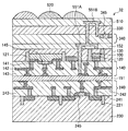
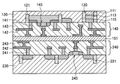
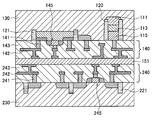
- FIG. 2 is a cross-sectional view showing an example in which the semiconductor device according to the same embodiment is applied to a stacked semiconductor device.
- FIG. 19 is a cross-sectional view showing another example in which the semiconductor device according to the same embodiment is applied to a stacked semiconductor device.
- FIG. 26 is a cross-sectional view showing still another example in which the semiconductor device according to the same embodiment is applied to a stacked semiconductor device.
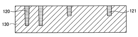
- FIG. 5 is a longitudinal cross-sectional view for schematically explaining one step of the first manufacturing method of the stacked semiconductor device.
- FIG. 5 is a longitudinal cross-sectional view for schematically explaining one step of the first manufacturing method of the stacked semiconductor device.
- FIG. 5 is a longitudinal cross-sectional view for schematically explaining one step of the first manufacturing method of the stacked semiconductor device.
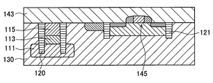
- FIG. 5 is a longitudinal cross-sectional view for schematically explaining one step of the first manufacturing method of the stacked semiconductor device.
- FIG. 5 is a longitudinal cross-sectional view for schematically explaining one step of the first manufacturing method of the stacked semiconductor device.
- FIG. 5 is a longitudinal cross-sectional view for schematically explaining one step of the first manufacturing method of the stacked semiconductor device.
- FIG. 5 is a longitudinal cross-sectional view for schematically explaining one step of the first manufacturing method of the stacked semiconductor device. It is a longitudinal cross-sectional view which illustrates typically 1 process of the 2nd manufacturing method of a lamination type semiconductor device. It is a longitudinal cross-sectional view which illustrates typically 1 process of the 2nd manufacturing method of a lamination type semiconductor device. It is a longitudinal cross-sectional view which illustrates typically 1 process of the 2nd manufacturing method of a lamination type semiconductor device. It is a longitudinal cross-sectional view which illustrates typically 1 process of the 2nd manufacturing method of a lamination type semiconductor device.
- FIG. 1 is an external view showing an example of an electronic device according to an embodiment of the present disclosure. It is an external view which shows the other example of the electronic device which concerns on the same embodiment. It is an external view which shows the further another example of the electronic device which concerns on the embodiment.
- FIG. 1 is a perspective view for explaining the configuration of a semiconductor device 100 according to the present embodiment.
- the semiconductor device 100 includes a first conductivity type layer 111, an intermediate layer 113, and a second conductivity type layer 115.
- the semiconductor device 100 may be covered with the separation layer 120 around the side surface for electrical insulation.
- the first conductivity type layer 111 is formed of a semiconductor material into which a first conductivity type impurity is introduced.
- the first conductivity type layer 111 may be formed of silicon (Si) into which an n-type impurity such as phosphorus (P) or arsenic (As) is introduced.
- the first conductivity type layer 111 is a silicon in which n-type impurities are introduced at a concentration of 1.0 ⁇ 10 16 / cm 3 to 1.0 ⁇ 10 19 / cm 3 using an ion implantation method or the like. It may be formed as a layer.
- the second conductivity type layer 115 is formed of a semiconductor material into which a second conductivity type impurity is introduced.
- the second conductivity type layer 115 may be formed of silicon (Si) into which a p-type impurity such as boron (B) or aluminum (Al) is introduced.
- the second conductivity type layer 115 is a silicon in which a p-type impurity is introduced at a concentration of 1.0 ⁇ 10 16 / cm 3 to 1.0 ⁇ 10 19 / cm 3 using an ion implantation method or the like. It may be formed as a layer.
- the first conductivity type impurity and the second conductivity type impurity represent conductivity type impurities having different polarities. Therefore, as exemplified above, when the first conductivity type impurity is an n-type impurity, the second conductivity type impurity is a p-type impurity. Conversely, when the first conductivity type impurity is a p-type impurity, the second conductivity type impurity is an n-type impurity.
- the intermediate layer 113 is provided between the first conductive type layer 111 and the second conductive type layer 115 in the stacking direction.
- the intermediate layer 113 is formed of a semiconductor material which does not contain a conductive impurity, or a semiconductor material which has a lower concentration of conductive impurities than the first conductive layer 111 or the second conductive layer 115.
- the intermediate layer 113 is a silicon layer not containing p-type impurities or n-type impurities, or the concentration of p-type impurities or n-type impurities contained in the first conductivity type layer 111 or the second conductivity type layer 115. Is a low silicon layer.
- the intermediate layer 113 is formed as a silicon layer in which n-type impurities are introduced at a concentration of 1.0 ⁇ 10 14 / cm 3 to 1.0 ⁇ 10 15 / cm 3 by ion implantation or the like. It may be done.
- the intermediate layer 113 is a layer characterized in that the doping concentration of the p-type impurity or the n-type impurity is lower than that of the first conductive type layer 111 and the second conductive type layer 115. It is not particularly limited whether or not an n-type impurity is contained.
- the first conductive type layer 111, the intermediate layer 113 and the second conductive type layer 115 described above are all formed of a semiconductor material, and in these layers, the presence or absence, type and concentration of conductive type impurities contained in the semiconductor material At least one is different. Therefore, the first conductivity type layer 111, the intermediate layer 113, and the second conductivity type layer 115 may be made of the same semiconductor material. For example, all of the first conductivity type layer 111, the intermediate layer 113, and the second conductivity type layer 115 may be formed of silicon.
- the first conductive type layer 111, the intermediate layer 113 and the second conductive type layer 115 may be made of a semiconductor material other than silicon.
- the first conductivity type layer 111, the intermediate layer 113, and the second conductivity type layer 115 may be other element semiconductors such as germanium (Ge) or gallium arsenide (GaAs), gallium nitride (GaN) or silicon carbide (SiC) And the like may be made of a compound semiconductor such as
- the separation layer 120 is provided with an insulating material so as to surround the side surface of the stack of the first conductivity type layer 111, the intermediate layer 113, and the second conductivity type layer 115.
- the separation layer 120 may be provided with an insulating material such as silicon oxide (SiO x ), silicon nitride (SiN x ), or silicon oxynitride (SiON).
- the separation layer 120 suppresses the leak current from the semiconductor device 100 by forming an electrical insulating layer on the side surface of the stacked body of the first conductivity type layer 111, the intermediate layer 113, and the second conductivity type layer 115. Can.
- the upper surface of the second conductive layer 115 and the lower surface of the first conductive layer 111 which face each other in the stacking direction, are separated. It is not covered with the layer 120 and is exposed.
- the exposed upper surface of the second conductivity type layer 115 and the lower surface of the first conductivity type layer 111 function as terminals of the semiconductor device 100, and can be electrically connected to various wirings through, for example, vias or the like.
- the exposed upper surface of the second conductivity type layer 115 and the lower surface of the first conductivity type layer 111 are doped with a higher concentration conductivity type impurity to reduce the contact resistance between the semiconductor device 100 and the via. May be
- the p-type semiconductor and the n-type semiconductor are interposed through the lightly doped or non-doped semiconductor layer (that is, the intermediate layer 113).
- a PIN structure is formed in which the first conductivity type layer 111 and the second conductivity type layer 115) are joined in the stacking direction.
- a depletion layer having an extremely low carrier concentration is formed from the first conductivity type layer 111 and the second conductivity type layer 115 toward the intermediate layer 113.
- the breakdown voltage can be increased by the depletion layer, so high withstand voltage can be ensured.
- the intermediate layer 113 needs to have a thickness of more than several ⁇ m.
- the planar area occupied by the semiconductor device 100 can be reduced as compared to the case where the PIN structure is formed in the planar direction. .
- a layer containing conductivity type impurities of different polarity is provided on the surface opposite to the surface on which the intermediate layer 113 of the first conductivity type layer 111 or the second conductivity type layer 115 is provided.
- a layer containing a second conductivity type impurity may be provided on the surface of the first conductivity type layer 111 opposite to the surface on which the intermediate layer 113 is provided.
- a layer containing a first conductivity type impurity may be provided on the surface of the second conductivity type layer 115 opposite to the surface on which the intermediate layer 113 is provided.
- the semiconductor device 100 has an NPIN (NP-Intrinsic-N) structure or PINP (P-Intrinsic-NP) in which the PN junction of a bipolar transistor having an NPN structure or a PNP structure is replaced with a PIN junction. It will have a structure. Also with this structure, the semiconductor device 100 can function as a high breakdown voltage element.
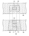
- FIG. 2 is a top view and a cross-sectional view for explaining the configuration of the semiconductor device 100 according to the present embodiment.
- the top view of the semiconductor device 100 in FIG. 2 is a top view of the semiconductor device 100
- the bottom view is a cross-sectional view of the semiconductor device 100.
- the semiconductor device 100 may be provided inside the semiconductor substrate 130 and electrically isolated from the semiconductor substrate 130 by the separation layer 120.
- the semiconductor substrate 130 is a substrate formed of a semiconductor material.
- the semiconductor substrate 130 may be a silicon substrate.
- the semiconductor substrate 130 is a silicon substrate that can be easily processed, the semiconductor device 100 can be more easily formed inside the semiconductor substrate 130.
- the semiconductor substrate 130 is a substrate formed of another elemental semiconductor such as germanium or a substrate formed of a compound semiconductor such as gallium arsenide (GaAs), gallium nitride (GaN) or silicon carbide (SiC), It is also good.
- GaAs gallium arsenide
- GaN gallium nitride
- SiC silicon carbide
- the semiconductor substrate 130 may be thinned by CMP (Chemical Mechanical Polishing) or the like.
- the semiconductor device 100 according to the present embodiment can be provided to penetrate the semiconductor substrate 130. Therefore, in order to make the pressure resistance of the semiconductor device 100 a desired characteristic, the thickness of the semiconductor substrate 130 is several ⁇ m to several tens of ⁇ m so that the thickness of the intermediate layer 113 falls within a range of several ⁇ m to several tens of ⁇ m.
- the thickness may be reduced to a certain extent, for example, about 2 ⁇ m to 20 ⁇ m. Since the thickness of a general semiconductor substrate 130 marketed for forming a semiconductor device is about several hundreds of ⁇ m, a semiconductor device having desired characteristics by thinning the semiconductor substrate 130 to the above range It is possible to form 100 more easily.
- the semiconductor device 100 is provided to penetrate the semiconductor substrate 130 in a stacked structure of the first conductivity type layer 111, the intermediate layer 113, and the second conductivity type layer 115.
- a predetermined conductivity type impurity (a first conductivity type impurity or a second conductivity type impurity or a second conductivity type) is formed in a region in the thickness direction of the semiconductor substrate 130 corresponding to the first conductivity type layer 111 and the second conductivity type layer 115. It can be formed by introducing any of conductive impurities.
- the region into which the first conductivity type impurity is introduced becomes the first conductivity type layer 111
- the region into which the second conductivity type impurity is introduced becomes the second conductivity type layer 115.
- the region sandwiched by the first conductive type layer 111 and the second conductive type layer 115 described above becomes the intermediate layer 113.
- the semiconductor device 100 Since the semiconductor device 100 is provided to penetrate the semiconductor substrate 130, the first conductivity type layer 111 and the second conductivity type layer 115 can be exposed on both opposing main surfaces of the semiconductor substrate 130, respectively. Thereby, in the semiconductor device 100, since the exposed first conductivity type layer 111 and the second conductivity type layer 115 can be used as a terminal of the PIN structure diode, electrical connection between the semiconductor device 100 and various wirings can be realized. It can be easily formed.
- the first conductive type layer 111 and the second conductive type layer 115 may not be exposed on both opposing main surfaces of the semiconductor substrate 130 from the time when they are formed.
- the first conductivity type layer 111 and the second conductivity type layer 115 are formed on the inside of the semiconductor substrate 130, and are then performed on both opposing main surfaces of the semiconductor substrate 130 by thinning of the semiconductor substrate 130 performed later. It may be exposed.
- the separation layer 120 is provided to penetrate the semiconductor substrate 130 so as to surround the side surface of the semiconductor device 100 provided as a stacked body of the first conductivity type layer 111, the intermediate layer 113, and the second conductivity type layer 115.
- the separation layer 120 can be formed by removing the semiconductor substrate 130 around the semiconductor device 100 by etching or the like and then embedding the removed region with an insulating material.
- the separation layer 120 may be formed by embedding an insulating material such as silicon oxide (SiO x ), silicon nitride (SiN x ), or silicon oxynitride (SiON) in the opening of the semiconductor substrate 130. That is, the separation layer 120 may be formed by the same method as a so-called STI (Shallow Trench Isolation) method.
- STI Shallow Trench Isolation
- the separation layer 120 may be formed by embedding an opening formed by etching from one main surface of the semiconductor substrate 130 with an insulating material, and is formed by etching from both opposing main surfaces of the semiconductor substrate 130. It may be formed by respectively embedding each of the formed openings with an insulating material.
- the etching direction at the time of forming the separation layer 120 can be determined by, for example, how the taper of the cross-sectional shape of the separation layer 120 in the thickness direction of the semiconductor substrate 130 is applied. Specifically, when the direction of the taper of the cross-sectional shape of the separation layer 120 is the same, it can be determined that the separation layer 120 is formed only by etching from one main surface of the semiconductor substrate 130. On the other hand, when the direction of the taper of the cross-sectional shape of the separation layer 120 is reversed in the middle, it can be determined that the separation layer 120 is formed by etching from each of both opposing main surfaces of the semiconductor substrate 130. . In the separation layer 120 shown in FIG. 2, since the direction of the taper of the cross-sectional shape of the separation layer 120 is constant, only by etching from one main surface of the semiconductor substrate 130 on the side on which the first conductivity type layer 111 is provided. It can be judged that it was formed.
- the semiconductor device 100 having such a configuration since the PIN structure can be provided in the thickness direction of the semiconductor substrate 130, the semiconductor device can be compared to the case where the PIN structure is provided in the in-plane direction of the semiconductor substrate 130. The planar area occupied by 100 can be reduced. Further, since the semiconductor device 100 is provided to penetrate the semiconductor substrate 130, electrical connection with various wirings can be easily formed.
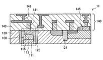
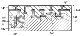
- FIGS. 3A to 4C are cross-sectional views showing an example in which the semiconductor device 100 according to the present embodiment is applied to a single-layer semiconductor device.
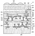
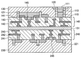
- 4A to 4C are cross-sectional views showing an example in which the semiconductor device 100 according to the present embodiment is applied to a stacked semiconductor device.
- the single-layer semiconductor device 11 includes one semiconductor substrate 130 and one multilayer wiring layer 140 formed on the semiconductor substrate 130.
- the semiconductor substrate 130 is, for example, a silicon substrate thinned to a thickness of several ⁇ m to several tens of ⁇ m (eg, 2 ⁇ m to 20 ⁇ m).
- the PIN diode 100 that is, the semiconductor device 100 described above
- the field effect transistor 145 and the like are provided to be separated by the separation layer 120 and the element separation layer 121.
- the PIN diode 100 is configured by stacking the first conductivity type layer 111, the intermediate layer 113, and the second conductivity type layer 115 in the thickness direction of the semiconductor substrate 130, and functions as a breakdown voltage element.
- the field effect transistor 145 is, for example, a MOSFET (Metal-Oxide-Semiconductor Field-Effect Transistor), and executes signal processing or the like in the single-layer semiconductor device 11.
- the field effect transistor 145 is an example of an active element and a passive element provided on the semiconductor substrate 130, and the element provided on the semiconductor substrate 130 is not limited to the field effect transistor 145. Further, the semiconductor substrate 130 may be provided with a plurality of other active elements and passive elements.
- the isolation layer 120 and the element isolation layer 121 are formed of, for example, an insulating material such as silicon oxide, and electrically isolate the PIN diode 100 and the field effect transistor 145 from each other so as not to conduct through the semiconductor substrate 130.
- the separation layer 120 is provided to penetrate the semiconductor substrate 130 in order to electrically separate the PIN diode 100.
- the element isolation layer 121 may not be provided through the semiconductor substrate 130, as long as the element isolation layer 121 has a predetermined depth at which the field effect transistor 145 can be electrically isolated.
- the multilayer wiring layer 140 is provided on the semiconductor substrate 130 by, for example, stacking a plurality of interlayer insulating films 143 made of an insulating material.
- a wiring layer 142 for transmitting a signal from, for example, the PIN diode 100 and the field effect transistor 145 is provided in the multilayer wiring layer 140, for example.
- the wiring layer 142 is electrically connected to the PIN diode 100 or the field effect transistor 145 or the like provided in the semiconductor substrate 130 by the via 141 provided in the lowermost layer.
- the wiring layer 142 can extract a signal from the PIN diode 100, the field effect transistor 145, and the like through the via 141.
- the interlayer insulating film 143 may be formed of, for example, a known insulating material such as SiO 2 or SiN.
- the interlayer insulating film 143 may be formed of one type of insulating material, or may be formed of a plurality of types of insulating materials.
- the wiring layer 142 may be formed of, for example, a metal material such as copper (Cu) or aluminum (Al), which has relatively low resistance, in order to enable faster signal transmission.
- the via 141 may be formed of, for example, a metal material such as tungsten (W) or the like that has a high embedding property to the opening at the time of film formation.
- the PIN diode 100 (that is, the above-described semiconductor device 100) can be applied to such a single layer semiconductor device 11 as a breakdown voltage element.
- the PIN diode 100 connects the first conductive type layer 111 exposed on the back surface of the semiconductor substrate 130 (that is, the surface opposite to the surface on which the multilayer wiring layer 140 is provided) to bumps or the like, It is possible to use it as a pressure protection element which protects an internal circuit from a surge voltage of
- the single-layer semiconductor device 12 includes one semiconductor substrate 130 and one multilayer interconnection layer 140 formed on the semiconductor substrate 130.
- a PIN diode 100A, a field effect transistor 145, and the like are provided to be separated by the separation layer 120A and the element separation layer 121.
- the PIN diode 100A is configured by laminating a first conductivity type layer 111A, an intermediate layer 113A, and a second conductivity type layer 115A in the thickness direction of the semiconductor substrate 130.
- each configuration of the single layer semiconductor device 12 shown in FIG. 3B is substantially the same as each configuration of the single layer semiconductor device 11 shown in FIG. It is similar. Therefore, the description of these configurations is omitted here.
- the single-layer semiconductor device 12 shown in FIG. 3B differs from the single-layer semiconductor device 11 shown in FIG. 3A only in the cross-sectional shapes of the PIN diode 100A and the separation layer 120A.
- the cross-sectional shapes of the PIN diode 100A and the separation layer 120A are hexagonal shapes in which the direction of the taper is reversed halfway through.
- the cross-sectional shapes of the PIN diode 100 and the separation layer 120 are trapezoidal in one direction.
- Such a difference in cross-sectional shape of the separation layer 120A can occur due to a difference in the process of forming the separation layer 120A.
- the formed opening has an inverse tapered shape in which the bottom portion has a smaller area than the top portion on the opening side.
- the separation layer 120A of the single layer type semiconductor device 12 shown in FIG. 3B is formed by embedding each of the openings by etching from both opposing main surfaces of the semiconductor substrate 130 with an insulating material, the taper direction is It becomes the cross-sectional shape of the inverted hexagonal shape.
- the separation layer 120 of the single-layer type semiconductor device 11 shown in FIG. 3A is formed by embedding the opening by etching from one main surface of the semiconductor substrate 130 with an insulating material, and therefore, it has a trapezoidal shape tapered in one direction. It becomes a shape.
- part of the separation layer 120A is formed simultaneously with the element separation layer 121 from the side of the semiconductor substrate 130 on which the field effect transistor 145 is formed.
- the remaining portion of the separation layer 120A is formed from the surface facing the surface on which the separation layer 121 is formed.
- the degree of difficulty of etching when forming the separation layer 120A is It can be reduced.
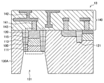
- the single-layer semiconductor device 13 includes one semiconductor substrate 130A and one multilayer wiring layer 140 formed on the semiconductor substrate 130A.
- a PIN diode 100 and a field effect transistor are provided by being separated by the separation layer 120 and the element separation layer 121.
- the PIN diode 100 is configured by laminating a first conductivity type layer 111, an intermediate layer 113, and a second conductivity type layer 115 in the thickness direction of the semiconductor substrate 130.
- the semiconductor substrate 130A is not thinned and has a thickness of about several hundred ⁇ m. Therefore, when the PIN diode 100 is formed to penetrate the semiconductor substrate 130A, the entire height of the PIN diode 100 is about several hundred ⁇ m, so that the PIN diode 100 having desired characteristics can be realized. It will be difficult.
- the PIN diode 100 is formed to a height having desired characteristics. Thereafter, by providing an opening 131 for exposing the PIN diode 100 from the surface facing the surface of the semiconductor substrate 130A on which the multilayer wiring layer 140 is provided, electrical connection to the PIN diode 100 is enabled.
- the semiconductor substrate 130 is not thinned and has a thickness of about several hundreds of ⁇ m, so that the mechanical strength of the single-layer semiconductor device 13 can be increased.
- the configuration of the single-layer semiconductor device 13 shown in FIG. 3C is substantially the same as the configuration of the single-layer semiconductor device 11 shown in FIG. 3A, except for the thickness of the semiconductor substrate 130A. Therefore, the description of these configurations is omitted here.
- the stacked semiconductor device 21 is formed on a semiconductor substrate 130 and a semiconductor substrate 230 and the semiconductor substrate 130.
- the substrate comprises a semiconductor substrate 130 and a multilayer wiring layer 140 formed on the semiconductor substrate 130.
- a substrate comprising the multilayer wiring layer 240. That is, the stacked semiconductor device 21 is a semiconductor device in which two semiconductor substrates are bonded to each other, and may be, for example, a back-illuminated solid-state imaging device.
- the substrate includes the semiconductor substrate 130 and the multilayer wiring layer 140 formed on the semiconductor substrate 130, and the semiconductor substrate 230 and the multilayer wiring layer 240 formed on the semiconductor substrate 230.
- the substrates are bonded such that the multilayer wiring layers 140 and 240 face each other (that is, in the face to face) with the insulating layer 151 interposed therebetween.
- the stacked semiconductor device 21 is bonded such that the semiconductor substrate 130 and the multilayer wiring layer 240 face each other, or the multilayer wiring layer 140 and the semiconductor substrate 230 face each other (that is, face to back). It goes without saying that it may be
- the semiconductor substrate 130 is, for example, a silicon substrate thinned to a thickness of several ⁇ m to several tens of ⁇ m (eg, 2 ⁇ m to 20 ⁇ m).
- the PIN diode 100 that is, the semiconductor device 100 described above
- the field effect transistor 145 and the like are provided to be separated by the separation layer 120 and the element separation layer 121.
- the PIN diode 100 is configured by laminating the first conductivity type layer, the intermediate layer, and the second conductivity type layer in the thickness direction of the semiconductor substrate 130, and functions as a breakdown voltage element.
- the field effect transistor 145 is, for example, a MOSFET, and executes signal processing and the like in the stacked semiconductor device 21.
- the field effect transistor 145 is an example of an active element and a passive element provided on the semiconductor substrate 130, and the element provided on the semiconductor substrate 130 is not limited to the field effect transistor 145. Further, the semiconductor substrate 130 may be provided with a plurality of other active elements and passive elements.
- the isolation layer 120 and the element isolation layer 121 are formed of, for example, an insulating material such as silicon oxide, are formed on the semiconductor substrate 130, and electrically isolate the PIN diode 100, the field effect transistor 145, and the like.
- the separation layer 120 is provided to penetrate the semiconductor substrate 130 in order to electrically separate the PIN diode 100.
- the element isolation layer 121 may not be provided to penetrate the semiconductor substrate 130.
- the multilayer wiring layer 140 is provided on the semiconductor substrate 130 by, for example, stacking a plurality of interlayer insulating films 143 made of an insulating material.
- a wiring layer 142 for transmitting a signal from, for example, the PIN diode 100 and the field effect transistor 145 is provided in the multilayer wiring layer 140, for example.
- the wiring layer 142 is electrically connected to the PIN diode 100 and the field effect transistor 145 provided in the semiconductor substrate 130 by the via 141 provided in the lowermost layer.
- the wiring layer 142 can extract a signal from the PIN diode 100, the field effect transistor 145, and the like through the via 141.
- the twin contacts 551 are provided on the surface of the semiconductor substrate 130 opposite to the surface on which the multilayer wiring layer 140 is provided, and the signal from the PIN diode 100 is taken out.
- the twin contact 551 is a metal such as copper (Cu) for an opening for exposing either the first conductivity type layer or the second conductivity type layer of the PIN diode 100 and an opening for exposing the wiring layer 142. It is formed by embedding with a material etc. and connecting both embedded.
- the interlayer insulating film 143 may be formed of, for example, a known insulating material such as SiO 2 or SiN.
- the interlayer insulating film 143 may be formed of one type of insulating material, or may be formed of a plurality of types of insulating materials.
- the wiring layer 142 may be formed of, for example, a metal material such as copper (Cu) or aluminum (Al) which has relatively low resistance. Thus, the wiring layer 142 can perform signal transmission at higher speed.
- the via 141 may be formed of, for example, a metal material such as tungsten (W) or the like that has a high embedding property to the opening at the time of film formation.
- the semiconductor substrate 230 is, for example, a silicon substrate.
- the semiconductor substrate 230 may be thinned or may not be thinned.
- the semiconductor substrate 230 is provided with, for example, a field effect transistor 245 and the like separated by an element isolation layer 221.
- the field effect transistor 245 is, for example, a MOSFET, and executes signal processing and the like in the stacked semiconductor device 21.
- the field effect transistor 245 is an example of an active element and a passive element provided on the semiconductor substrate 230, and the element provided on the semiconductor substrate 230 is not limited to the field effect transistor 245. Further, the semiconductor substrate 230 may be provided with a plurality of other active elements and passive elements.
- the element isolation layer 221 is formed of, for example, an insulating material such as silicon oxide, and electrically isolates the field effect transistor 245 and the like formed on the semiconductor substrate 230 from each other.
- the multilayer wiring layer 240 is provided on the semiconductor substrate 230 by, for example, stacking a plurality of interlayer insulating films 243 made of an insulating material.
- a wiring layer 242 for transmitting a signal from the field effect transistor 245 or the like is provided in the inside of the multilayer wiring layer 240.
- the wiring layer 242 is electrically connected to the field effect transistor 245 or the like provided in the semiconductor substrate 230 by the via 241 provided in the lowermost layer.
- the wiring layer 242 can extract a signal from the field effect transistor 245 or the like through the via 241.
- the interlayer insulating film 243 may be formed of, for example, a known insulating material such as SiO x or SiN x .
- the interlayer insulating film 243 may be formed of one type of insulating material, or may be formed of a plurality of types of insulating materials.
- the wiring layer 242 may be formed of, for example, a metal material such as copper (Cu) or aluminum (Al), which has relatively low resistance, in order to enable faster signal transmission.
- the vias 241 may be formed of, for example, a metal material such as tungsten (W) that has a high ability to be embedded in the opening during film formation.
- the insulating layer 151 is formed of, for example, a known insulating material such as SiO x or SiN x, and is provided between the multilayer wiring layer 140 and the multilayer wiring layer 240.
- the insulating layer 151 electrically insulates the wiring layer 142 in the multilayer wiring layer 140 and the wiring layer 242 in the multilayer wiring layer 240.
- the electrical connection between the wiring layer 142 in the multilayer wiring layer 140 and the wiring layer 242 in the multilayer wiring layer 240 can be formed by a known method.
- the electrical connection between the wiring layer 142 in the multilayer wiring layer 140 and the wiring layer 242 in the multilayer wiring layer 240 may be, for example, a contact via provided through the insulating layer 151, a plurality of through holes It is possible to form a twin contact via in which an electrical connection is formed by embedding the conductive material with a conductive material, and an electrode junction structure in which an electrical connection is formed by joining electrodes exposed on the bonding surface. is there.
- the pad 533 is a metal layer exposed by the opening 531 and functions as an input / output unit (I / O unit) of the stacked semiconductor device 21. By connecting a wire bonding or the like to the pad 533, an electrical connection between the stacked semiconductor device 21 and the external circuit can be formed.
- the pad 533 may be formed of, for example, a metal material such as aluminum (Al) which facilitates electrical connection by wire bonding or the like.
- the insulating layer 510 is provided on the side opposite to the surface of the semiconductor substrate 130 on which the multilayer wiring layer 140 is provided, and functions as a protective layer that protects the internal circuits and the like of the stacked semiconductor device 21.
- the insulating layer 510 may be formed of a transparent insulating material such as, for example, SiO x , SiN x , Al 2 O 3 or TiO 2 .
- the microlens 520 is provided when the stacked semiconductor device 21 is a solid-state imaging device, and condenses light from an imaging target to improve the sensitivity of the solid-state imaging device.
- the microlens 520 is provided with a color filter having any of red, green and blue colors in order to enable imaging in color. It may be
- the PIN diode 100 (that is, the above-described semiconductor device 100) can be applied to the stacked semiconductor device 21 having such a two-layer stacked structure as a breakdown voltage element.
- the stacked semiconductor device 21 since the multilayer wiring layer or the semiconductor substrate is provided on both opposing main surfaces of the semiconductor substrate 130 on which the PIN diode 100 is provided, electrical connection with the PIN diode 100 is more easily formed. can do.
- the PIN diode 100 can be used as a withstand voltage protection element that protects the internal circuit from the surge voltage generated in the stacked semiconductor device 21.
- the stacked semiconductor device 31 is formed on a semiconductor substrate 130 and a semiconductor substrate 230 and the semiconductor substrate 230, the substrate including the semiconductor substrate 130 and the multilayer wiring layer 140 formed on the semiconductor substrate 130. And a substrate formed of a semiconductor substrate 330 and a multilayer wiring layer 340 formed on the semiconductor substrate 330. That is, the stacked semiconductor device 31 is a semiconductor device in which three semiconductor substrates are bonded to each other, and may be, for example, a back-illuminated solid-state imaging device.
- the substrate includes the semiconductor substrate 130 and the multilayer wiring layer 140 formed on the semiconductor substrate 130, and the semiconductor substrate 230 and the multilayer wiring layer 240 formed on the semiconductor substrate 230.
- the substrates are pasted together such that the multilayer wiring layers 140 and 240 face each other with the insulating layer 151 interposed therebetween.
- the substrate formed of the semiconductor substrate 130 and the multilayer wiring layer 140 formed on the semiconductor substrate 130 is insulated from the substrate formed of the semiconductor substrate 330 and the multilayer wiring layer 340 formed on the semiconductor substrate 330.
- the semiconductor substrate 130 and the multilayer wiring layer 340 are attached to face each other through the layer 152.
- the PIN diode 100 can be electrically connected to the field effect transistor 345 or the like provided in the multilayer wiring layer 340 by the electrode junction structure 552.
- the configurations having the same names and the same reference numerals as the configuration described in the stacked semiconductor device 21 shown in FIG. 4A are substantially described in the stacked semiconductor device 21 shown in FIG. Since it is as it is, description here is abbreviate
- the semiconductor substrate 330 is, for example, a silicon substrate thinned to a thickness of several ⁇ m to several tens of ⁇ m (for example, 2 ⁇ m to 20 ⁇ m).
- the semiconductor substrate 330 is provided with, for example, a field effect transistor 345 or the like.
- the field effect transistor 345 is, for example, a MOSFET, and executes signal processing and the like in the stacked semiconductor device 31.
- the field effect transistor 345 is an example of an active element and a passive element provided on the semiconductor substrate 330, and the element provided on the semiconductor substrate 330 is not limited to the field effect transistor 345. Further, the semiconductor substrate 330 may be provided with a plurality of other active elements and passive elements.
- the multilayer wiring layer 340 is provided on the semiconductor substrate 230 by laminating a plurality of interlayer insulating films made of a known insulating material such as SiO x or SiN x , for example.
- a wiring layer (not shown) that transmits a signal from, for example, a field effect transistor 345 or the like may be provided inside the multilayer wiring layer 340.
- the wiring layer is electrically connected to a field effect transistor 345 or the like provided in the semiconductor substrate 330 by a via (not shown) provided in the lowermost layer.
- the wiring layer and the via may be formed of, for example, a metal material such as copper (Cu), aluminum (Al) or (W) which has relatively low resistance.
- the insulating layer 152 is formed of, for example, a known insulating material such as SiO x or SiN x , and is provided between the multilayer wiring layer 340 and the semiconductor substrate 130.
- the insulating layer 152 electrically insulates the multilayer wiring layer 340 and the semiconductor substrate 130.
- the electrode bonding structure 552 is an electrical connection structure formed by bonding electrodes exposed on the bonding surfaces of the insulating layer 152 and the multilayer wiring layer 340. Specifically, the electrode bonding structure 552 brings an electrode made of copper (Cu) formed in the insulating layer 152 into contact with an electrode made of copper (Cu) formed in the multilayer wiring layer 340, and both are processed by heat treatment. Formed by joining together.
- the PIN diode 100 can be applied as a breakdown voltage element also to the stacked semiconductor device 31 having such a three-layer stacked structure. Further, the structure for forming the electrical connection between the multilayer wiring layer 340 and the PIN diode 100 or the multilayer wiring layer 140 is not limited to the above-described electrode junction structure 552, and various structures such as contact vias or twin contact vias are used. It is also possible.
- the PIN diode 100 is provided inside the semiconductor substrate 130.
- the PIN diode 100 may be provided inside the semiconductor substrate 230 or the semiconductor substrate 330. Needless to say.
- the stacked semiconductor device 32 is formed on a semiconductor substrate 130 and a semiconductor substrate 230 and the semiconductor substrate 230.
- the substrate comprises the semiconductor substrate 130 and the multilayer wiring layer 140 formed on the semiconductor substrate 130.
- the substrate includes the semiconductor substrate 130 and the multilayer wiring layer 140 formed on the semiconductor substrate 130, and the semiconductor substrate 230 and the multilayer wiring layer 240 formed on the semiconductor substrate 230.
- the substrates are pasted together such that the multilayer wiring layers 140 and 240 face each other with the insulating layer 151 interposed therebetween.
- the substrate formed of the semiconductor substrate 130 and the multilayer wiring layer 140 formed on the semiconductor substrate 130 is insulated from the substrate formed of the semiconductor substrate 330 and the multilayer wiring layer 340 formed on the semiconductor substrate 330.
- the semiconductor substrate 130 and the multilayer wiring layer 340 are attached to face each other through the layer 152.
- the PIN diode 100 is electrically connected to the field effect transistor 345 provided on the multilayer wiring layer 340 by the twin contacts 551A and 551B, and the wiring layer 142 provided on the multilayer wiring layer 140. Can be connected.
- the configurations having the same names and the same reference numerals as those of the stacked semiconductor devices 21 and 31 shown in FIGS. 4A and 4B substantially correspond to the stacked layers shown in FIGS. Since it is as having demonstrated by the type
- the twin contacts 551A and 551B are provided on the surface of the semiconductor substrate 130 opposite to the surface on which the multilayer wiring layer 140 is provided, and the signal from the PIN diode 100 is extracted.
- an opening for exposing either the first conductivity type layer or the second conductivity type layer of the PIN diode 100 and an opening for exposing the wiring layer 142 are metal such as copper (Cu) or the like. It is formed by embedding with a material etc. and connecting both embedded.
- the twin contact 551B is formed by embedding the opening for exposing the twin contact 551A and the opening for exposing the terminal of the field effect transistor 345 with a metal material such as copper (Cu) and connecting the embedded Ru.
- the PIN diode 100 can be applied as a breakdown voltage element also to the stacked semiconductor device 32 having such a three-layer stacked structure.
- FIGS. 5A to 5E are longitudinal cross-sectional views for schematically explaining the steps of the first method of manufacturing the stacked semiconductor device 21. First, as shown in FIG.
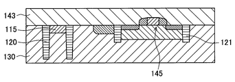
- the separation layer 120 and the element separation layer 121 are formed in a predetermined region of the semiconductor substrate 130.
- the opening is formed by etching a predetermined region of one main surface of the semiconductor substrate 130 made of silicon or the like. After that, the opening formed by etching is filled with an insulating material and planarized to form the separation layer 120 and the element separation layer 121.
- the separation layer 120 is formed to a region which is equal to or deeper than the depth at which the element separation layer 121 is formed.
- an interlayer insulating film 143 is formed on the semiconductor substrate 130.
- the second conductivity type layer 115 is formed by ion-implanting a second conductivity type impurity into a region surrounded by the separation layer 120 of the semiconductor substrate 130 and performing heat treatment.
- the field effect transistor 145 is formed in a region surrounded by the element isolation layer 121 of the semiconductor substrate 130 by a known method.
- an interlayer insulating film 143 is formed using silicon oxide or the like on the one main surface on which the second conductivity type layer 115 of the semiconductor substrate 130 and the field effect transistor 145 are formed.
- the heat treatment at the time of forming the second conductivity type layer 115 may be performed simultaneously with the heat treatment for the other components.
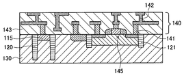
- the multilayer wiring layer 140 is formed on the semiconductor substrate 130.
- the multilayer wiring layer 140 is formed on the semiconductor substrate 130 by repeating the film formation of the interlayer insulating film 143, the formation of the wiring layer 142, and the formation of the via 141 penetrating the interlayer insulating film 143.
- the materials described above can be used.
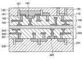
- the semiconductor substrate 130 on which the multilayer wiring layer 140 is formed in the above process and the semiconductor substrate 230 on which the multilayer wiring layer 240 is formed in the same process are interposed through the insulating layer 151. Paste it together. Specifically, the semiconductor substrate 130 on which the multilayer wiring layer 140 is formed and the semiconductor substrate 230 on which the multilayer wiring layer 240 is formed are bonded so that the multilayer wiring layers 140 and 240 face each other. At this time, by providing the insulating layer 151 on the bonding surface of the multilayer wiring layers 140 and 240, the wiring layer 142 in the multilayer wiring layer 140 and the wiring layer 242 in the multilayer wiring layer 240 are electrically insulated. The electrical connection (not shown) between the wiring layer 142 in the multilayer wiring layer 140 and the wiring layer 242 in the multilayer wiring layer 240 can be formed separately using a known method.
- the semiconductor substrate 130 is thinned by polishing the semiconductor substrate 130 until the separation layer 120 is exposed. Specifically, the surface of the semiconductor substrate 130 opposite to the surface on which the multilayer wiring layer 140 is provided is polished using CMP or the like until the separation layer 120 is exposed, so that the semiconductor substrate 130 is several ⁇ m to several tens of ⁇ m. The thickness is reduced to about ⁇ m (eg, 2 ⁇ m to 20 ⁇ m).
- the first conductivity type layer 111 is formed in a predetermined region of the semiconductor substrate 130. Specifically, the first conductive type impurity is ion-implanted in a region surrounded by the separation layer 120 of the semiconductor substrate 130, and heat treatment is performed to form the first conductive type layer 111.
- the first conductivity type layer 111 is formed in a region of a depth not in contact with the second conductivity type layer 115, and a region between the first conductivity type layer 111 and the second conductivity type layer 115 is an intermediate layer 113.
- a semiconductor device 100 in which the first conductivity type layer 111, the intermediate layer 113, and the second conductivity type layer 115 are stacked, and a stacked semiconductor device including the semiconductor device 100 can be formed.
- FIGS. 6A to 6E are vertical cross-sectional views for explaining each step of the second method for manufacturing the stacked semiconductor device 21. First, as shown in FIG.
- the separation layer 120 and the element separation layer 121 are formed in a predetermined region of the semiconductor substrate 130.
- the opening is formed by etching a predetermined region of one main surface of the semiconductor substrate 130 made of silicon or the like. After that, the opening formed by etching is filled with an insulating material and planarized to form the separation layer 120 and the element separation layer 121.
- the separation layer 120 is formed to a region which is equal to or deeper than the depth at which the element separation layer 121 is formed.
- an interlayer is formed on the semiconductor substrate 130.
- the insulating film 143 is formed.
- the first conductive type impurity and the second conductive type impurity are respectively ion-implanted in a region surrounded by the separation layer 120 of the semiconductor substrate 130, and heat treatment is performed to form the first conductive type layer 111 and the second conductive type impurity.
- a two conductivity type layer 115 is formed.
- the depth at which the first conductivity type layer 111 and the second conductivity type layer 115 are formed can be controlled by the energy of the first conductivity type impurity and the second conductivity type impurity at the time of ion implantation. Therefore, by controlling the conditions of ion implantation, it is possible to form a stacked structure of the first conductivity type layer 111, the intermediate layer 113, and the second conductivity type layer 115. Further, the field effect transistor 145 is formed in a region surrounded by the element isolation layer 121 of the semiconductor substrate 130 by a known method. Thereafter, an interlayer insulating film 143 is formed using silicon oxide or the like on the one main surface on which the second conductivity type layer 115 of the semiconductor substrate 130 and the field effect transistor 145 are formed.
- a multilayer wiring layer 140 is formed on the semiconductor substrate 130.
- the multilayer wiring layer 140 is formed on the semiconductor substrate 130 by repeating the film formation of the interlayer insulating film 143, the formation of the wiring layer 142, and the formation of the via 141 penetrating the interlayer insulating film 143.
- the materials described above can be used.
- the semiconductor substrate 130 on which the multilayer wiring layer 140 is formed in the above process and the semiconductor substrate 230 on which the multilayer wiring layer 240 is formed in the same process are interposed through the insulating layer 151. Paste it together. Specifically, the semiconductor substrate 130 on which the multilayer wiring layer 140 is formed and the semiconductor substrate 230 on which the multilayer wiring layer 240 is formed are bonded so that the multilayer wiring layers 140 and 240 face each other. At this time, by providing the insulating layer 151 on the bonding surface of the multilayer wiring layers 140 and 240, the wiring layer 142 in the multilayer wiring layer 140 and the wiring layer 242 in the multilayer wiring layer 240 are electrically insulated. The electrical connection (not shown) between the wiring layer 142 in the multilayer wiring layer 140 and the wiring layer 242 in the multilayer wiring layer 240 can be formed separately using a known method.
- the semiconductor substrate 130 is thinned by polishing the semiconductor substrate 130 until the first conductivity type layer 111 is exposed. Specifically, the surface of the semiconductor substrate 130 opposite to the surface provided with the multilayer wiring layer 140 is polished using CMP or the like until the first conductive type layer 111 is exposed, so that the number of semiconductor substrates 130 can be increased. The thickness is reduced to a thickness of about ⁇ m to several tens of ⁇ m (eg, 2 ⁇ m to 20 ⁇ m). As a result, a semiconductor device 100 in which the first conductivity type layer 111, the intermediate layer 113, and the second conductivity type layer 115 are stacked, and a stacked semiconductor device including the semiconductor device 100 can be formed.
- FIGS. 7A to 7E are schematic longitudinal sectional views for explaining the steps of the third method of manufacturing the stacked semiconductor device 21. First, as shown in FIG.
- the separation layer 120 of which a part is the diffusion layer 123 and the element separation layer 121 are formed.
- the opening is formed by etching a predetermined region of one main surface of the semiconductor substrate 130 made of silicon or the like.
- the diffusion layer 123 is formed by embedding a part of the opening with a material obtained by adding the first conductive type impurity to the inorganic insulator, and then the remaining part of the opening is embedded
- the separation layer 120 is formed by planarization.
- the opening where the element isolation layer 121 is formed the opening is filled with an insulating material and the element isolation layer 121 is formed by planarization.
- the first conductivity type impurity contained in the diffusion layer 123 is solid phase diffused to form the first conductivity type layer 111.
- a stacked structure of the first conductivity type layer 111, the intermediate layer 113, and the second conductivity type layer 115 can be formed.
- the field effect transistor 145 is formed in a region surrounded by the element isolation layer 121 of the semiconductor substrate 130 by a known method. Thereafter, an interlayer insulating film 143 is formed using silicon oxide or the like on the one main surface on which the second conductivity type layer 115 of the semiconductor substrate 130 and the field effect transistor 145 are formed.
- the multilayer wiring layer 140 is formed on the semiconductor substrate 130.
- the multilayer wiring layer 140 is formed on the semiconductor substrate 130 by repeating the film formation of the interlayer insulating film 143, the formation of the wiring layer 142, and the formation of the via 141 penetrating the interlayer insulating film 143.
- the materials described above can be used.
- the semiconductor substrate 130 on which the multilayer wiring layer 140 is formed in the above process and the semiconductor substrate 230 on which the multilayer wiring layer 240 is formed in the same process are interposed through the insulating layer 151. Paste it together. Specifically, the semiconductor substrate 130 on which the multilayer wiring layer 140 is formed and the semiconductor substrate 230 on which the multilayer wiring layer 240 is formed are bonded so that the multilayer wiring layers 140 and 240 face each other. At this time, by providing the insulating layer 151 on the bonding surface of the multilayer wiring layers 140 and 240, the wiring layer 142 in the multilayer wiring layer 140 and the wiring layer 242 in the multilayer wiring layer 240 are electrically insulated. The electrical connection (not shown) between the wiring layer 142 in the multilayer wiring layer 140 and the wiring layer 242 in the multilayer wiring layer 240 can be formed separately using a known method.
- the semiconductor substrate 130 is thinned by polishing the semiconductor substrate 130 until the separation layer 120 is exposed. Specifically, the surface of the semiconductor substrate 130 opposite to the surface provided with the multilayer wiring layer 140 is polished using CMP or the like until the separation layer 120 is exposed, whereby the semiconductor substrate 130 is several ⁇ m to several ⁇ m The thickness is reduced to about 10 ⁇ m (eg, 2 ⁇ m to 20 ⁇ m). As a result, a semiconductor device 100 in which the first conductivity type layer 111, the intermediate layer 113, and the second conductivity type layer 115 are stacked, and a stacked semiconductor device including the semiconductor device 100 can be formed.
- Electronic devices according to an embodiment of the present disclosure are various electronic devices in which a circuit including the semiconductor device 100 described above is mounted.
- An example of the electronic device according to the present embodiment will be described with reference to FIGS. 8A to 8C.
- 8A to 8C are external views showing an example of the electronic device according to the present embodiment.
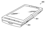
- the electronic device may be an electronic device such as a smartphone.
- the smartphone 900 includes a display unit 901 that displays various information, and an operation unit 903 configured of a button or the like that receives an operation input by the user.
- the semiconductor device 100 according to an embodiment of the present disclosure may be provided in a control circuit that controls various operations of the smartphone 900.
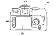
- the electronic device may be an electronic device such as a digital camera.
- the digital camera 910 includes a main body (camera body) 911, an interchangeable lens unit 913, a grip 915 gripped by the user at the time of photographing, A monitor unit 917 for displaying information and an EVF (Electronic View Finder) 919 for displaying a through image observed by the user at the time of shooting are provided.
- 8B is an external view of the digital camera 910 as viewed from the front (ie, object side)
- FIG. 8C is an external view of the digital camera 910 as viewed from the rear (ie, photographer side).
- the semiconductor device 100 according to an embodiment of the present disclosure may be provided.
- the electronic device which concerns on this embodiment is not limited to the said illustration.
- the electronic device according to the present embodiment may be an electronic device in any field.
- an electronic device for example, a glasses-type wearable device, an HMD (Head Mounted Display), a television device, an electronic book, a PDA (Personal Digital Assistant), a notebook personal computer, a video camera, a game device, etc. are illustrated. be able to.
- the semiconductor device 100 according to an embodiment of the present disclosure functions as a breakdown voltage element that withstands higher voltages. Therefore, the semiconductor device 100 according to an embodiment of the present disclosure can be more suitably used for an electronic device in an in-vehicle field or an IoT field in which a higher voltage power source is used in an internal circuit.
- the semiconductor device 100 according to the embodiment of the present disclosure the PIN structure including the first conductive type layer 111, the intermediate layer 113, and the second conductive type layer 115 in the stacking direction is formed. be able to. Therefore, the semiconductor device 100 according to the present embodiment can further reduce the occupied area in the planar direction as compared with the case where the PIN structure is formed in the planar direction. Therefore, the semiconductor device 100 according to the present embodiment can provide a withstand voltage element that can withstand a higher voltage with a more efficient occupied area.
- the semiconductor device 100 according to the present embodiment is applied to a solid-state imaging device in the above embodiment, the present technology is not limited to such an example.
- the semiconductor device 100 according to the present embodiment may be applied to a logic circuit, a memory device, or various sensor devices.
- the semiconductor device according to (1) further including a separation layer separating the first conductivity type layer, the intermediate layer, the second conductivity type layer, and the semiconductor substrate from each other.
- (4) The laminate of the first conductivity type layer, the intermediate layer, and the second conductivity type layer is provided to penetrate the semiconductor substrate in the thickness direction, according to any one of (1) to (3).
- Semiconductor devices (5) The semiconductor device according to (4), wherein the first conductivity type layer and the second conductivity type layer are exposed on both opposing main surfaces of the semiconductor substrate.
- the semiconductor device according to (4) wherein at least one of the first conductivity type layer and the second conductivity type layer is exposed by an opening provided in the semiconductor substrate.
- the intermediate layer has a concentration lower than the concentration of the first conductivity type impurity or the second conductivity type impurity of the first conductivity type layer and the second conductivity type layer, the first conductivity type impurity or the second.
- the semiconductor device according to any one of the above (1) to (6) which contains a conductive impurity.
- (8) The above (1) to (1), wherein the first conductive type layer or the second conductive type layer is electrically connected to a via provided in a multilayer wiring layer formed on any of the main surfaces of the semiconductor substrate.
- the semiconductor device is A first conductivity type layer having a first conductivity type impurity introduced therein; A second conductivity type layer introduced with a second conductivity type impurity different in polarity from the first conductivity type impurity;
- the first conductive type layer and the second conductive type layer are sandwiched, and do not contain the first conductive type impurity or the second conductive type impurity, or the concentration of the first conductive type impurity or the second conductive type impurity
- An intermediate layer having a lower value than the first conductive type layer and the second conductive type layer; Equipped with The electronic device, wherein the first conductive type layer, the intermediate layer, and the second conductive type layer are provided stacked in the thickness direction of the semiconductor substrate.
Landscapes
- Semiconductor Integrated Circuits (AREA)
- Element Separation (AREA)
- Solid State Image Pick-Up Elements (AREA)
- Metal-Oxide And Bipolar Metal-Oxide Semiconductor Integrated Circuits (AREA)
- Internal Circuitry In Semiconductor Integrated Circuit Devices (AREA)
Abstract
【課題】より効率的な占有面積で、より高電圧に耐えられる半導体装置を提供する。 【解決手段】第1導電型不純物が導入された第1導電型層と、前記第1導電型不純物と極性が異なる第2導電型不純物が導入された第2導電型層と、前記第1導電型層及び前記第2導電型層に挟持され、前記第1導電型不純物又は前記第2導電型不純物を含まない、又は前記第1導電型不純物又は前記第2導電型不純物の濃度が前記第1導電型層及び第2導電型層よりも低い中間層と、を備え、前記第1導電型層、前記中間層及び前記第2導電型層は、半導体基板の内部に前記半導体基板の厚み方向に積層されて設けられる、半導体装置。
Description
本開示は、半導体装置及び電子機器に関する。
近年、IoT(Internet of Things)分野及び自動車分野にて使用される半導体装置において、電源の高電圧化が進んでいる。このため、このような半導体装置において、内部回路を保護するために入出力部(I/O部ともいう)等に設けられる耐圧素子には、より高いサージ電圧に耐えることが求められている。
例えば、一般的な耐圧素子として、P型半導体及びN型半導体を接合したPN接合ダイオードが知られている。しかしながら、PN接合ダイオードは、ブレークダウン電圧が低いため、上述したような高耐圧性が求められる耐圧素子への適用は困難であった。
ここで、高耐圧性を有する耐圧素子としては、例えば、下記の特許文献1に開示されるように、低ドーズの中間層を介してP型半導体及びN型半導体を接合したPIN(P-Intrinsic-N)構造のダイオードが提案されている。PIN構造のダイオードでは、低ドーズの中間層と、P型半導体及びN型半導体との間で空乏層が形成されるため、形成された空乏層によってP型半導体及びN型半導体の間の電界が緩和される。これにより、PIN構造のダイオードは、PN接合ダイオードよりもブレークダウン電圧を高くすることができるため、より高耐圧性の耐圧素子に適用することが可能となる。
しかし、特許文献1に開示された耐圧素子は、半導体基板の面内方向にPIN構造が形成されるため、半導体基板内での耐圧素子の占有面積が大きくなり、半導体装置の微細化に不向きであった。特に、入出力部ごとに耐圧素子を設ける場合、占有面積の大きな耐圧素子は、半導体装置のチップサイズを縮小する際の制約になっていた。
また、PIN構造のダイオードでブレークダウン電圧をより高くするためには、P型半導体及びN型半導体との間に形成される空乏層の幅をより大きくする必要がある。したがって、より高耐圧性が要求される耐圧素子ほど占有面積が大きくなり、半導体装置が大型化してしまう可能性があった。
そこで、より効率的な占有面積で、より高電圧に耐えられる半導体装置が求められていた。
本開示によれば、第1導電型不純物が導入された第1導電型層と、前記第1導電型不純物と極性が異なる第2導電型不純物が導入された第2導電型層と、前記第1導電型層及び前記第2導電型層に挟持され、前記第1導電型不純物又は前記第2導電型不純物を含まない、又は前記第1導電型不純物又は前記第2導電型不純物の濃度が前記第1導電型層及び第2導電型層よりも低い中間層と、を備え、前記第1導電型層、前記中間層及び前記第2導電型層は、半導体基板の内部に前記半導体基板の厚み方向に積層されて設けられる、半導体装置が提供される。
また、本開示によれば、半導体基板の内部に設けられた半導体装置を含み、前記半導体装置は、第1導電型不純物が導入された第1導電型層と、前記第1導電型不純物と極性が異なる第2導電型不純物が導入された第2導電型層と、前記第1導電型層及び前記第2導電型層に挟持され、前記第1導電型不純物又は前記第2導電型不純物を含まない、又は前記第1導電型不純物又は前記第2導電型不純物の濃度が前記第1導電型層及び第2導電型層よりも低い中間層と、を備え、前記第1導電型層、前記中間層及び前記第2導電型層は、前記半導体基板の厚み方向に積層されて設けられる、電子機器が提供される。
本開示によれば、積層方向に、第1導電型不純物を含む第1導電型層と、導電型不純物を含まない、又は導電型不純物を低濃度で含む中間層と、第2導電型不純物を含む第2導電型層とからなるPIN構造を形成することができる。
以上説明したように本開示によれば、より効率的な占有面積で、より高電圧に耐えられる半導体装置を提供することが可能である。
なお、上記の効果は必ずしも限定的なものではなく、上記の効果とともに、または上記の効果に代えて、本明細書に示されたいずれかの効果、または本明細書から把握され得る他の効果が奏されてもよい。
以下に添付図面を参照しながら、本開示の好適な実施の形態について詳細に説明する。なお、本明細書及び図面において、実質的に同一の機能構成を有する構成要素については、同一の符号を付することにより重複説明を省略する。
なお、説明は以下の順序で行うものとする。
1.半導体装置の構成
2.半導体装置の適用例
2.1.単層型半導体装置への適用例
2.2.積層型半導体装置への適用例
3.半導体装置の製造方法
3.1.第1の製造方法
3.2.第2の製造方法
3.3.第3の製造方法
4.電子機器
5.まとめ
1.半導体装置の構成
2.半導体装置の適用例
2.1.単層型半導体装置への適用例
2.2.積層型半導体装置への適用例
3.半導体装置の製造方法
3.1.第1の製造方法
3.2.第2の製造方法
3.3.第3の製造方法
4.電子機器
5.まとめ
<1.半導体装置の構成>
まず、図1を参照して、本開示の一実施形態に係る半導体装置の構成について説明する。図1は、本実施形態に係る半導体装置100の構成を説明する斜視図である。
まず、図1を参照して、本開示の一実施形態に係る半導体装置の構成について説明する。図1は、本実施形態に係る半導体装置100の構成を説明する斜視図である。
図1に示すように、半導体装置100は、第1導電型層111と、中間層113と、第2導電型層115と、を備える。また、半導体装置100は、電気的な絶縁のために、側面の周囲を分離層120で覆われていてもよい。
第1導電型層111は、第1導電型不純物が導入された半導体材料にて形成される。具体的には、第1導電型層111は、リン(P)又はヒ素(As)などのn型不純物が導入されたシリコン(Si)にて形成されてもよい。例えば、第1導電型層111は、イオン注入法などを用いて、n型不純物を1.0×10¹⁶個/cm3~1.0×1019個/cm3の濃度で導入されたシリコン層として形成されてもよい。
第2導電型層115は、第2導電型不純物が導入された半導体材料にて形成される。具体的には、第2導電型層115は、ホウ素(B)又はアルミニウム(Al)などのp型不純物が導入されたシリコン(Si)にて形成されてもよい。例えば、第2導電型層115は、イオン注入法などを用いて、p型不純物を1.0×10¹⁶個/cm3~1.0×1019個/cm3の濃度で導入されたシリコン層として形成されてもよい。
本実施形態に係る半導体装置100において、第1導電型不純物と、第2導電型不純物とは、互いに極性が異なる導電型不純物を表す。したがって、上記で例示したように、第1導電型不純物がn型不純物である場合、第2導電型不純物はp型不純物である。逆に、第1導電型不純物がp型不純物である場合、第2導電型不純物はn型不純物である。
中間層113は、第1導電型層111及び第2導電型層115の間に、積層方向に挟持されて設けられる。中間層113は、導電型不純物を含まない半導体材料、又は第1導電型層111若しくは第2導電型層115よりも含まれる導電型不純物の濃度が低い半導体材料にて形成される。
具体的には、中間層113は、p型不純物又はn型不純物を含まないシリコン層、又は第1導電型層111又は第2導電型層115よりも含まれるp型不純物又はn型不純物の濃度が低いシリコン層であってもよい。例えば、中間層113は、イオン注入法などを用いて、n型不純物を1.0×10¹⁴個/cm3~1.0×1015個/cm3の濃度で導入されたシリコン層として形成されてもよい。なお、中間層113は、第1導電型層111及び第2導電型層115よりもp型不純物又はn型不純物のドーピング濃度が低いことを特徴とする層であり、中間層113にp型不純物又はn型不純物が含まれるか否かは特に限定されない。
上記の第1導電型層111、中間層113及び第2導電型層115は、いずれも半導体材料で形成され、これらの層では、該半導体材料に含まれる導電型不純物の有無、種類及び濃度の少なくともいずれかが異なる。そのため、第1導電型層111、中間層113及び第2導電型層115は、同一の半導体材料で構成されてもよい。例えば、第1導電型層111、中間層113及び第2導電型層115は、いずれもシリコンで形成されてもよい。
ただし、第1導電型層111、中間層113及び第2導電型層115は、シリコン以外の半導体材料で構成されてもよいことは言うまでもない。例えば、第1導電型層111、中間層113及び第2導電型層115は、ゲルマニウム(Ge)などの他の元素半導体、又はガリウムヒ素(GaAs)、窒化ガリウム(GaN)若しくはシリコンカーバイド(SiC)等の化合物半導体で構成されてもよい。
分離層120は、第1導電型層111、中間層113及び第2導電型層115の積層体の側面を取り囲むように絶縁材料にて設けられる。例えば、分離層120は、酸化シリコン(SiOx)、窒化シリコン(SiNx)又は酸窒化シリコン(SiON)などの絶縁材料にて設けられてもよい。分離層120は、第1導電型層111、中間層113及び第2導電型層115の積層体の側面に電気的な絶縁層を形成することによって、半導体装置100からのリーク電流を抑制することができる。
第1導電型層111、中間層113及び第2導電型層115からなる積層体において、積層方向に互いに対向する第2導電型層115の上面、及び第1導電型層111の下面は、分離層120にて覆われておらず、露出される。露出された第2導電型層115の上面、及び第1導電型層111の下面は、半導体装置100の端子として機能し、例えば、ビア等を介して各種配線と電気的に接続され得る。露出された第2導電型層115の上面、及び第1導電型層111の下面は、半導体装置100とビアとの接触抵抗を低減するために、より高濃度の導電型不純物にてドーピングされていてもよい。
これらの構成により、本実施形態に係る半導体装置100では、低濃度でドーピングされた、又はドーピングされていない半導体層(すなわち、中間層113)を介して、p型半導体及びn型半導体(すなわち、第1導電型層111及び第2導電型層115)が積層方向にて接合されたPIN構造が形成される。PIN構造では、第1導電型層111及び第2導電型層115から中間層113に向かって、キャリア濃度が極めて低い空乏層が形成される。本実施形態に係る半導体装置100では、該空乏層によって、ブレークダウン電圧を上昇させることができるため、高耐圧性を確保することができる。
例えば、PIN構造ダイオードにおいて、PN接合ダイオードの耐圧性(例えば、10V程度)を超える高耐圧性(例えば、20V超)を達成するためには、中間層113は、数μmを超える厚みが必要となる。本実施形態に係る半導体装置100では、PIN構造を積層方向に形成することによって、PIN構造が平面方向に形成された場合と比較して、半導体装置100が占有する平面面積を縮小することができる。
なお、半導体装置100では、第1導電型層111又は第2導電型層115の中間層113が設けられた面と対向する面に、異なる極性の導電型不純物を含む層が設けられていてもよい。具体的には、第1導電型層111の中間層113が設けられた面と対向する面には、第2導電型不純物を含む層が設けられていてもよい。または、第2導電型層115の中間層113が設けられた面と対向する面には、第1導電型不純物を含む層が設けられていてもよい。このような場合、半導体装置100は、NPN構造又はPNP構造を備えるバイポーラトランジスタのPN接合をPIN接合に置き換えたNPIN(N-P-Intrinsic-N)構造又はPINP(P-Intrinsic-N-P)構造を備えることになる。この構造によっても、半導体装置100は、高耐圧素子として機能することが可能である。
次に、図2を参照して、本実施形態に係る半導体装置100のより具体的な構成について説明する。図2は、本実施形態に係る半導体装置100の構成を説明する上面図及び断面図である。なお、図2を正対視して上側の図が半導体装置100の上面図であり、下側の図が半導体装置100の断面図である。
図2に示すように、例えば、半導体装置100は、半導体基板130の内部に設けられ、分離層120によって半導体基板130と電気的に絶縁されてもよい。
半導体基板130は、半導体材料で形成された基板である。例えば、半導体基板130は、シリコン基板であってもよい。半導体基板130が容易に加工可能なシリコン基板である場合、半導体基板130の内部における半導体装置100の形成をより容易に行うことができる。ただし、半導体基板130は、ゲルマニウムなどの他の元素半導体で形成された基板、又はガリウムヒ素(GaAs)、窒化ガリウム(GaN)若しくはシリコンカーバイド(SiC)等の化合物半導体で形成された基板であってもよい。
また、半導体基板130は、CMP(Chemical Mechanical Polishing)等によって薄肉化されていてもよい。本実施形態に係る半導体装置100は、半導体基板130を貫通して設けられ得る。したがって、半導体装置100の耐圧性を所望の特性とするためには、半導体基板130の厚みは、中間層113の厚みが数μm~数十μmの範囲に収まるように、数μm~数十μm程度に薄肉化されてもよく、例えば、2μm~20μm程度に薄肉化されてもよい。半導体装置の形成のために市販されている一般的な半導体基板130の厚さは、数百μm程度であるため、半導体基板130を上記範囲まで薄肉化することで、所望の特性を備える半導体装置100をより容易に形成することが可能である。
半導体装置100は、上述したように、第1導電型層111、中間層113及び第2導電型層115の積層構造にて、半導体基板130を貫通して設けられる。具体的には、半導体装置100は、第1導電型層111及び第2導電型層115に対応する半導体基板130の厚み方向の領域に、所定の導電型不純物(第1導電型不純物又は第2導電型不純物のいずれか)を導入することで、形成することができる。すなわち、半導体基板130のうち、第1導電型不純物が導入された領域が第1導電型層111となり、第2導電型不純物が導入された領域が第2導電型層115となる。また、半導体基板130の厚み方向で、前述の第1導電型層111及び第2導電型層115によって挟持された領域が中間層113となる。
半導体装置100は、半導体基板130を貫通して設けられるため、第1導電型層111及び第2導電型層115は、それぞれ半導体基板130の対向する両主面にて露出され得る。これにより、半導体装置100では、露出された第1導電型層111及び第2導電型層115をPIN構造ダイオードの端子として用いることができるため、半導体装置100と各種配線との電気的な接続を容易に形成することができる。
ただし、第1導電型層111及び第2導電型層115は、形成された時点から半導体基板130の対向する両主面にて露出されていなくともよい。例えば、第1導電型層111及び第2導電型層115は、半導体基板130の内部に形成された後、後段で行われる半導体基板130の薄肉化によって、半導体基板130の対向する両主面に露出されてもよい。
分離層120は、第1導電型層111、中間層113及び第2導電型層115の積層体として設けられた半導体装置100の側面を囲むように、半導体基板130を貫通して設けられる。具体的には、分離層120は、半導体装置100の周囲の半導体基板130をエッチング等で除去した後、除去した領域を絶縁材料で埋め込むことで形成することができる。例えば、分離層120は、酸化シリコン(SiOx)、窒化シリコン(SiNx)又は酸窒化シリコン(SiON)などの絶縁材料を半導体基板130の開口に埋め込むことで形成されてもよい。すなわち、分離層120は、いわゆるSTI(Shallow Trench Isolation)法と同様の方法によって形成されてもよい。
ここで、分離層120は、半導体基板130の一主面からのエッチングによって形成された開口を絶縁材料で埋め込むことで形成されてもよく、半導体基板130の対向する両主面からのエッチングによって形成された開口の各々を絶縁材料でそれぞれ埋め込むことで形成されてもよい。
分離層120の形成時におけるエッチング方向は、例えば、半導体基板130の厚み方向における分離層120の断面形状のテーパの掛かり方によって判断することが可能である。具体的には、分離層120の断面形状のテーパの向きが同一である場合、分離層120は、半導体基板130の一主面からのエッチングのみにて形成されたと判断することができる。一方、分離層120の断面形状のテーパの向きが途中で反転している場合、分離層120は、半導体基板130の対向する両主面の各々からのエッチングにて形成されたと判断することができる。図2で示す分離層120は、分離層120の断面形状のテーパの向きが一定であるため、第1導電型層111が設けられた側の半導体基板130の一主面からのエッチングのみにて形成されたと判断することができる。
このような構成を備える半導体装置100によれば、半導体基板130の厚み方向にPIN構造を設けることができるため、半導体基板130の面内方向にPIN構造を設けた場合と比較して、半導体装置100の占有する平面面積を縮小させることができる。また、半導体装置100は、半導体基板130を貫通して設けられるため、各種配線との電気的接続を容易に形成することができる。
<2.半導体装置の適用例>
続いて、図3A~図4Cを参照して、本実施形態に係る半導体装置100の適用例について説明する。図3A~図3Cは、本実施形態に係る半導体装置100を単層型半導体装置に適用した一例を示す断面図である。図4A~図4Cは、本実施形態に係る半導体装置100を積層型半導体装置に適用した一例を示す断面図である。
続いて、図3A~図4Cを参照して、本実施形態に係る半導体装置100の適用例について説明する。図3A~図3Cは、本実施形態に係る半導体装置100を単層型半導体装置に適用した一例を示す断面図である。図4A~図4Cは、本実施形態に係る半導体装置100を積層型半導体装置に適用した一例を示す断面図である。
(2.1.単層型半導体装置への適用例)
まず、図3A~図3Cを参照して、本実施形態に係る半導体装置100の単層型半導体装置への適用例について説明する。
まず、図3A~図3Cを参照して、本実施形態に係る半導体装置100の単層型半導体装置への適用例について説明する。
図3Aに示すように、単層型半導体装置11は、1つの半導体基板130と、半導体基板130の上に形成された1つの多層配線層140と、を備える。
半導体基板130は、例えば、数μm~数十μm(例えば、2μm~20μm)の厚みに薄肉化されたシリコン基板である。半導体基板130には、例えば、PINダイオード100(すなわち、上述した半導体装置100)及び電界効果トランジスタ145等が分離層120及び素子分離層121によって離隔されて設けられる。
PINダイオード100は、上述したように、半導体基板130の厚み方向に第1導電型層111、中間層113及び第2導電型層115が積層されることで構成され、耐圧素子として機能する。電界効果トランジスタ145は、例えば、MOSFET(Metal-Oxide-Semiconductor Field-Effect Transistor)であり、単層型半導体装置11における信号処理等を実行する。
なお、電界効果トランジスタ145は、半導体基板130に設けられる能動素子及び受動素子の一例であり、半導体基板130に設けられる素子が電界効果トランジスタ145に限定されるわけではない。また、半導体基板130には、他の能動素子及び受動素子が複数設けられていてもよい。
分離層120及び素子分離層121は、例えば、酸化シリコンなどの絶縁材料で形成され、PINダイオード100及び電界効果トランジスタ145が半導体基板130を介して導通しないように、互いを電気的に離隔する。なお、分離層120は、PINダイオード100を電気的に離隔するために、半導体基板130を貫通して設けられる。一方、素子分離層121は、半導体基板130を貫通して設けられなくともよく、電界効果トランジスタ145を電気的に離隔することができる所定の深さまで設けられていればよい。
多層配線層140は、例えば、絶縁材料からなる複数の層間絶縁膜143を積層することで、半導体基板130の上に設けられる。加えて、多層配線層140の内部には、例えば、PINダイオード100及び電界効果トランジスタ145等からの信号を伝達する配線層142が設けられる。配線層142は、最下層に設けられたビア141によって、半導体基板130に設けられたPINダイオード100又は電界効果トランジスタ145等と電気的に接続される。配線層142は、ビア141を介してPINダイオード100及び電界効果トランジスタ145等から信号を取り出すことができる。
層間絶縁膜143は、例えば、SiO2又はSiN等の公知の絶縁材料によって形成されてもよい。また、層間絶縁膜143は、1種の絶縁材料によって形成されてもよく、複数種の絶縁材料によって形成されてもよい。配線層142は、より高速での信号伝達を可能とするために、例えば、比較的低抵抗である銅(Cu)又はアルミニウム(Al)などの金属材料によって形成されてもよい。ビア141は、例えば、成膜時における開口への埋め込み性が高いタングステン(W)等の金属材料によって形成されてもよい。
このような単層型半導体装置11に対して、PINダイオード100(すなわち、上述した半導体装置100)を耐圧素子として適用することができる。PINダイオード100は、例えば、半導体基板130の裏面(すなわち、多層配線層140が設けられた面と対向する面)に露出した第1導電型層111をバンプ等に接続することで、外部回路からのサージ電圧から内部回路を保護する耐圧保護素子として使用することが可能である。
次に、図3Bを参照して、単層型半導体装置の他の例について説明する。
図3Bに示すように、単層型半導体装置12は、1つの半導体基板130と、半導体基板130の上に形成された1つの多層配線層140と、を備える。半導体基板130には、例えば、PINダイオード100A及び電界効果トランジスタ145等が、分離層120A及び素子分離層121によって離隔されて設けられる。PINダイオード100Aは、半導体基板130の厚み方向に第1導電型層111A、中間層113A及び第2導電型層115Aが積層されることで構成される。
なお、PINダイオード100A及び分離層120Aの断面形状以外の構成については、図3Bに示す単層型半導体装置12の各構成は、図3Aに示す単層型半導体装置11の各構成と実質的に同様である。よって、これらの構成についての説明はここでは省略する。
図3Bに示す単層型半導体装置12は、図3Aに示す単層型半導体装置11と比較して、PINダイオード100A及び分離層120Aの断面形状のみが異なる。具体的には、図3Bに示す単層型半導体装置12では、PINダイオード100A及び分離層120Aの断面形状は、途中からテーパの向きが反転した六角形形状となっている。一方、図3Aに示す単層型半導体装置11では、PINダイオード100及び分離層120の断面形状は、一方向のテーパが掛かった台形形状となっている。
このような分離層120Aの断面形状の差異は、分離層120Aの形成工程の差異によって生じ得る。具体的には、アスペクト比が高い開口をエッチングにて形成する場合、形成された開口は、底部の方が開口側の上部よりも面積が小さい逆テーパ形状となる。
図3Bに示す単層型半導体装置12の分離層120Aは、半導体基板130の対向する両主面からのエッチングによる開口の各々を絶縁材料で埋め込むことで形成されるため、途中からテーパの向きが反転した六角形形状の断面形状となる。一方、図3Aに示す単層型半導体装置11の分離層120は、半導体基板130の一主面からのエッチングによる開口を絶縁材料で埋め込むことで形成されるため、一方向のテーパが掛かった台形形状となる。
図3Bに示す単層型半導体装置12では、半導体基板130の電界効果トランジスタ145が形成された面側から素子分離層121と同時に分離層120Aの一部を形成し、その後、半導体基板130の素子分離層121を形成した面と対向する面から分離層120Aの残部を形成する。これにより、図3Bに示す単層型半導体装置12では、半導体基板130を貫通する分離層120Aを形成することができる。
図3Bに示す単層型半導体装置12では、分離層120Aの形成時に半導体基板130を貫通する高アスペクト比の開口を形成しなくともよいため、分離層120Aを形成する際のエッチングの難易度を低減することができる。
さらに、図3Cを参照して、単層型半導体装置のさらに他の例について説明する。
図3Cに示すように、単層型半導体装置13は、1つの半導体基板130Aと、半導体基板130Aの上に形成された1つの多層配線層140と、を備える。半導体基板130Aには、例えば、PINダイオード100及び電界効果トランジスタ(図示せず)等が、分離層120及び素子分離層121によって離隔されて設けられる。PINダイオード100は、半導体基板130の厚み方向に第1導電型層111、中間層113及び第2導電型層115が積層されることで構成される。
ここで、図3Cに示す単層型半導体装置13では、半導体基板130Aは、薄肉化されておらず、数百μm程度の厚みを有する。したがって、半導体基板130Aを貫通するようにPINダイオード100を形成した場合、PINダイオード100の全体の高さが数百μm程度になってしまうため、所望の特性を有するPINダイオード100を実現することが困難となる。
そこで、図3Cに示す単層型半導体装置13では、まず、PINダイオード100を所望の特性を有する高さに形成する。その後、半導体基板130Aの多層配線層140が設けられた面と対向する面からPINダイオード100を露出させる開口131を設けることで、PINダイオード100への電気的な接続を可能とする。
図3Cに示す単層型半導体装置13では、半導体基板130が薄肉化されず、数百μm程度の厚みを有するため、単層型半導体装置13の機械的強度を高めることが可能である。
なお、半導体基板130Aの厚み以外の構成については、図3Cに示す単層型半導体装置13の各構成は、図3Aに示す単層型半導体装置11の各構成と実質的に同様である。よって、これらの構成についての説明はここでは省略する。
(2.2.積層型半導体装置への適用例)
次に、図4A~図4Cを参照して、本実施形態に係る半導体装置100の積層型半導体装置への適用例について説明する。
次に、図4A~図4Cを参照して、本実施形態に係る半導体装置100の積層型半導体装置への適用例について説明する。
図4Aに示すように、積層型半導体装置21は、半導体基板130及び該半導体基板130の上に形成された多層配線層140からなる基板と、半導体基板230及び該半導体基板130の上に形成された多層配線層240からなる基板とを備える。すなわち、積層型半導体装置21は、2つの半導体基板を貼り合わせた半導体装置であり、例えば、裏面照射型固体撮像装置であってもよい。
積層型半導体装置21では、半導体基板130及び該半導体基板130の上に形成された多層配線層140からなる基板と、半導体基板230及び該半導体基板230の上に形成された多層配線層240からなる基板とが、絶縁層151を介して互いの多層配線層140、240が対向するように(すなわち、Face to Faceにて)貼り合わされている。ただし、積層型半導体装置21は、半導体基板130と多層配線層240とが対向するように、又は多層配線層140と半導体基板230とが対向するように(すなわち、Face to Backにて)貼り合わされていてもよいことは言うまでもない。
半導体基板130は、例えば、数μm~数十μm(例えば、2μm~20μm)の厚みに薄肉化されたシリコン基板である。半導体基板130には、例えば、PINダイオード100(すなわち、上述した半導体装置100)及び電界効果トランジスタ145等が分離層120及び素子分離層121によって離隔されて設けられる。
PINダイオード100は、上述したように、半導体基板130の厚み方向に第1導電型層、中間層及び第2導電型層が積層されることで構成され、耐圧素子として機能する。電界効果トランジスタ145は、例えば、MOSFETであり、積層型半導体装置21における信号処理等を実行する。
なお、電界効果トランジスタ145は、半導体基板130に設けられる能動素子及び受動素子の一例であり、半導体基板130に設けられる素子が電界効果トランジスタ145に限定されるわけではない。また、半導体基板130には、他の能動素子及び受動素子が複数設けられていてもよい。
分離層120及び素子分離層121は、例えば、酸化シリコンなどの絶縁材料で形成され、半導体基板130に形成されPINダイオード100及び電界効果トランジスタ145等を電気的に離隔する。なお、分離層120は、PINダイオード100を電気的に離隔するために、半導体基板130を貫通して設けられる。一方、素子分離層121は、半導体基板130を貫通して設けられなくともよい。
多層配線層140は、例えば、絶縁材料からなる複数の層間絶縁膜143を積層することで、半導体基板130の上に設けられる。加えて、多層配線層140の内部には、例えば、PINダイオード100及び電界効果トランジスタ145等からの信号を伝達する配線層142が設けられる。配線層142は、最下層に設けられたビア141によって、半導体基板130に設けられたPINダイオード100及び電界効果トランジスタ145等と電気的に接続される。配線層142は、ビア141を介してPINダイオード100及び電界効果トランジスタ145等から信号を取り出すことができる。
ツインコンタクト551は、半導体基板130の多層配線層140が設けられた面と対向する面に設けられ、PINダイオード100からの信号を取り出す。具体的には、ツインコンタクト551は、PINダイオード100の第1導電型層又は第2導電型層のいずれかを露出させる開口と、配線層142を露出させる開口とを銅(Cu)などの金属材料等で埋め込み、埋め込んだ両者を接続することで形成される。
層間絶縁膜143は、例えば、SiO2又はSiN等の公知の絶縁材料によって形成されてもよい。また、層間絶縁膜143は、1種の絶縁材料によって形成されてもよく、複数種の絶縁材料によって形成されてもよい。配線層142は、例えば、比較的低抵抗である銅(Cu)又はアルミニウム(Al)などの金属材料によって形成されてもよい。これにより、配線層142は、より高速での信号伝達が可能となる。ビア141は、例えば、成膜時における開口への埋め込み性が高いタングステン(W)等の金属材料によって形成されてもよい。
半導体基板230は、例えば、シリコン基板である。半導体基板230は、薄肉化されていてもよく、薄肉化されていなくともよい。半導体基板230には、例えば、電界効果トランジスタ245等が素子分離層221によって離隔されて設けられる。電界効果トランジスタ245は、例えば、MOSFETであり、積層型半導体装置21における信号処理等を実行する。
なお、電界効果トランジスタ245は、半導体基板230に設けられる能動素子及び受動素子の一例であり、半導体基板230に設けられる素子が電界効果トランジスタ245に限定されるわけではない。また、半導体基板230には、他の能動素子及び受動素子が複数設けられていてもよい。
素子分離層221は、例えば、酸化シリコンなどの絶縁材料で形成され、半導体基板230に形成された電界効果トランジスタ245等を互いに電気的に離隔する。
多層配線層240は、例えば、絶縁材料からなる複数の層間絶縁膜243を積層することで、半導体基板230の上に設けられる。加えて、多層配線層240の内部には、例えば、電界効果トランジスタ245等からの信号を伝達する配線層242が設けられる。配線層242は、最下層に設けられたビア241によって、半導体基板230に設けられた電界効果トランジスタ245等と電気的に接続される。配線層242は、ビア241を介して電界効果トランジスタ245等から信号を取り出すことができる。
層間絶縁膜243は、例えば、SiOx又はSiNx等の公知の絶縁材料によって形成されてもよい。また、層間絶縁膜243は、1種の絶縁材料によって形成されてもよく、複数種の絶縁材料によって形成されてもよい。配線層242は、より高速での信号伝達を可能とするために、例えば、比較的低抵抗である銅(Cu)又はアルミニウム(Al)などの金属材料によって形成されてもよい。ビア241は、例えば、成膜時における開口への埋め込み性が高いタングステン(W)等の金属材料によって形成されてもよい。
絶縁層151は、例えば、SiOx又はSiNx等の公知の絶縁材料によって形成され、多層配線層140と、多層配線層240との間に設けられる。絶縁層151は、多層配線層140内の配線層142と、多層配線層240内の配線層242とを電気的に絶縁する。
なお、多層配線層140内の配線層142と、多層配線層240内の配線層242との間の電気的な接続は、公知の方法にて形成することが可能である。例えば、多層配線層140内の配線層142と、多層配線層240内の配線層242との間の電気的な接続は、例えば、絶縁層151を貫通して設けられるコンタクトビア、複数の貫通孔を導電材料で埋め込むことで電気的な接続を形成したツインコンタクトビア、貼り合わせ面に露出させた電極同士を接合することで電気的な接続を形成した電極接合構造などによって形成することが可能である。
パッド533は、開口531によって露出された金属層であり、積層型半導体装置21の入出力部(I/O部)として機能する。パッド533にワイヤボンディング等を接続することによって、積層型半導体装置21と外部回路との間の電気的な接続を形成することができる。パッド533は、例えば、ワイヤボンディングなどによる電気的接続が容易なアルミニウム(Al)などの金属材料にて形成されてもよい。
絶縁層510は、半導体基板130の多層配線層140が設けられた面と対向する面側に設けられ、積層型半導体装置21の内部回路等を保護する保護層として機能する。絶縁層510は、例えば、SiOx、SiNx、Al2O3又はTiO2等の透明な絶縁材料で形成されてもよい。
マイクロレンズ520は、積層型半導体装置21が固体撮像装置である場合に設けられ、撮像対象からの光を集光することで、固体撮像装置の感度を向上させる。また、積層型半導体装置21が固体撮像装置である場合、カラーでの撮像を可能とするために、マイクロレンズ520には、それぞれ赤色、緑色又は青色のいずれかの色を有するカラーフィルタが設けられていてもよい。
このような2層積層構造の積層型半導体装置21に対して、PINダイオード100(すなわち、上述した半導体装置100)を耐圧素子として適用することができる。積層型半導体装置21では、PINダイオード100が設けられる半導体基板130の対向する両主面に、それぞれ多層配線層又は半導体基板が設けられるため、より容易にPINダイオード100との電気的な接続を形成することができる。これによれば、PINダイオード100は、積層型半導体装置21にて発生するサージ電圧から内部回路を保護する耐圧保護素子として使用することが可能である。
なお、図4Aに示す積層型半導体装置21では、PINダイオード100が半導体基板130の内部に設けられる例を示したが、PINダイオード100は、半導体基板230の内部に設けられてもよいことは言うまでもない。
次に、図4Bを参照して、積層型半導体装置の他の例について説明する。
図4Bに示すように、積層型半導体装置31は、半導体基板130及び該半導体基板130の上に形成された多層配線層140からなる基板と、半導体基板230及び該半導体基板230の上に形成された多層配線層240からなる基板と、半導体基板330及び該半導体基板330の上に形成された多層配線層340からなる基板と、を備える。すなわち、積層型半導体装置31は、3つの半導体基板を貼り合わせた半導体装置であり、例えば、裏面照射型固体撮像装置であってもよい。
積層型半導体装置31では、半導体基板130及び該半導体基板130の上に形成された多層配線層140からなる基板と、半導体基板230及び該半導体基板230の上に形成された多層配線層240からなる基板とが、絶縁層151を介して互いの多層配線層140、240が対向するように貼り合わされている。一方、半導体基板130及び該半導体基板130の上に形成された多層配線層140からなる基板と、半導体基板330及び該半導体基板330の上に形成された多層配線層340からなる基板とは、絶縁層152を介して半導体基板130及び多層配線層340が対向するように貼り合わされている。
図4Bに示す積層型半導体装置31では、PINダイオード100は、電極接合構造552によって、多層配線層340に設けられた電界効果トランジスタ345等と電気的に接続され得る。図4Bに示す積層型半導体装置31において、図4Aに示す積層型半導体装置21にて説明した構成と同名及び同符号の構成は、実質的に図4Aに示す積層型半導体装置21にて説明したとおりであるため、ここでの説明は省略する。
半導体基板330は、例えば、数μm~数十μm(例えば、2μm~20μm)の厚みに薄肉化されたシリコン基板である。半導体基板330には、例えば、電界効果トランジスタ345等が設けられる。電界効果トランジスタ345は、例えば、MOSFETであり、積層型半導体装置31における信号処理等を実行する。
なお、電界効果トランジスタ345は、半導体基板330に設けられる能動素子及び受動素子の一例であり、半導体基板330に設けられる素子が電界効果トランジスタ345に限定されるわけではない。また、半導体基板330には、他の能動素子及び受動素子が複数設けられていてもよい。
多層配線層340は、例えば、SiOx又はSiNx等の公知の絶縁材料からなる複数の層間絶縁膜を積層することで、半導体基板230の上に設けられる。加えて、多層配線層340の内部には、例えば、電界効果トランジスタ345等からの信号を伝達する配線層(図示せず)が設けられてもよい。配線層は、最下層に設けられたビア(図示せず)によって、半導体基板330に設けられた電界効果トランジスタ345等と電気的に接続される。なお、配線層及びビアは、例えば、比較的低抵抗である銅(Cu)、アルミニウム(Al)又は(W)等の金属材料によって形成されてもよい。
絶縁層152は、例えば、SiOx又はSiNx等の公知の絶縁材料によって形成され、多層配線層340と、半導体基板130との間に設けられる。絶縁層152は、多層配線層340と、半導体基板130とを電気的に絶縁する。
電極接合構造552は、絶縁層152及び多層配線層340の貼り合わせ面に露出させた電極同士を接合することで形成された電気的接続構造である。具体的には、電極接合構造552は、絶縁層152に形成された銅(Cu)からなる電極と、多層配線層340に形成された銅(Cu)からなる電極とを接触させ、熱処理によって両者を接合することで形成される。
このような3層積層構造の積層型半導体装置31に対しても、PINダイオード100を耐圧素子として適用することができる。また、多層配線層340と、PINダイオード100又は多層配線層140との電気的接続を形成する構造は、上記の電極接合構造552に限定されず、コンタクトビア又はツインコンタクトビアなど多様な構造を用いることも可能である。
図4Bに示す積層型半導体装置31では、PINダイオード100は、半導体基板130の内部に設けられる例を示したが、PINダイオード100は、半導体基板230又は半導体基板330の内部に設けられてもよいことは言うまでもない。
続いて、図4Cを参照して、積層型半導体装置のさらに他の例について説明する。
図4Cに示すように、積層型半導体装置32は、半導体基板130及び該半導体基板130の上に形成された多層配線層140からなる基板と、半導体基板230及び該半導体基板230の上に形成された多層配線層240からなる基板と、半導体基板330及び該半導体基板330の上に形成された多層配線層340からなる基板と、を備える。すなわち、積層型半導体装置32は、3つの半導体基板を貼り合わせた半導体装置であり、例えば、裏面照射型固体撮像装置であってもよい。
積層型半導体装置32では、半導体基板130及び該半導体基板130の上に形成された多層配線層140からなる基板と、半導体基板230及び該半導体基板230の上に形成された多層配線層240からなる基板とが、絶縁層151を介して互いの多層配線層140、240が対向するように貼り合わされている。一方、半導体基板130及び該半導体基板130の上に形成された多層配線層140からなる基板と、半導体基板330及び該半導体基板330の上に形成された多層配線層340からなる基板とは、絶縁層152を介して半導体基板130及び多層配線層340が対向するように貼り合わされている。
図4Cに示す積層型半導体装置32では、PINダイオード100は、ツインコンタクト551A、551Bによって、多層配線層340に設けられた電界効果トランジスタ345、及び多層配線層140に設けられた配線層142と電気的に接続され得る。図4Cに示す積層型半導体装置32において、図4A及び図4Bに示す積層型半導体装置21、31にて説明した構成と同名及び同符号の構成は、実質的に図4A及び図4Bに示す積層型半導体装置21、31にて説明したとおりであるため、ここでの説明は省略する。
ツインコンタクト551A、551Bは、半導体基板130の多層配線層140が設けられた面と対向する面に設けられ、PINダイオード100からの信号を取り出す。具体的には、ツインコンタクト551Aは、PINダイオード100の第1導電型層又は第2導電型層のいずれかを露出させる開口と、配線層142を露出させる開口とを銅(Cu)などの金属材料等で埋め込み、埋め込んだ両者を接続することで形成される。また、ツインコンタクト551Bは、ツインコンタクト551Aを露出させる開口と、電界効果トランジスタ345の端子を露出させる開口とを銅(Cu)などの金属材料等で埋め込み、埋め込んだ両者を接続することで形成される。
このような3層積層構造の積層型半導体装置32に対しても、PINダイオード100を耐圧素子として適用することができる。
<3.半導体装置の製造方法>
次に、図5A~図7Eを参照して、図4Aに示す積層型半導体装置21の製造方法を説明する。
次に、図5A~図7Eを参照して、図4Aに示す積層型半導体装置21の製造方法を説明する。
(3.1.第1の製造方法)
図5A~図5Eを参照して、積層型半導体装置21の第1の製造方法について説明する。図5A~図5Eは、積層型半導体装置21の第1の製造方法の各工程を模式的に説明する縦断面図である。
図5A~図5Eを参照して、積層型半導体装置21の第1の製造方法について説明する。図5A~図5Eは、積層型半導体装置21の第1の製造方法の各工程を模式的に説明する縦断面図である。
まず、図5Aに示すように、半導体基板130の所定の領域に、分離層120及び素子分離層121を形成する。具体的には、シリコンなどで構成された半導体基板130の一主面の所定の領域をエッチングすることで、開口を形成する。その後、エッチングによって形成された開口を絶縁材料で埋め込み、平坦化することで分離層120及び素子分離層121を形成する。なお、分離層120は、素子分離層121が形成された深さと同等又はよりも深い領域まで形成される。
次に、図5Bに示すように、半導体基板130の所定の領域に、第2導電型層115、及び電界効果トランジスタ145を形成した後、半導体基板130の上に層間絶縁膜143を形成する。具体的には、半導体基板130の分離層120にて囲まれた領域に、第2導電型不純物をイオン注入し、熱処理することで、第2導電型層115を形成する。また、半導体基板130の素子分離層121にて囲まれた領域に、公知の方法によって電界効果トランジスタ145を形成する。その後、半導体基板130の第2導電型層115、及び電界効果トランジスタ145が形成された一主面の上に、酸化シリコンなどを用いて層間絶縁膜143を形成する。なお、第2導電型層115を形成する際の熱処理は、他の構成に対する熱処理と同時に行われてもよい。
続いて、図5Cに示すように、半導体基板130の上に多層配線層140が形成される。具体的には、層間絶縁膜143の成膜、配線層142の形成、及び層間絶縁膜143を貫通するビア141の形成を繰り返すことで、半導体基板130の上に多層配線層140を形成する。層間絶縁膜143、配線層142及びビア141を形成する材料は、上述した材料を用いることが可能である。
次に、図5Dに示すように、上記工程にて多層配線層140が形成された半導体基板130と、同様の工程にて多層配線層240が形成された半導体基板230とを絶縁層151を介して貼り合わせる。具体的には、多層配線層140が形成された半導体基板130と、多層配線層240が形成された半導体基板230とを互いの多層配線層140、240が対向するように貼り合わせる。このとき、多層配線層140、240の貼り合わせ面に絶縁層151を設けることで、多層配線層140内の配線層142と、多層配線層240内の配線層242とを電気的に絶縁する。多層配線層140内の配線層142と、多層配線層240内の配線層242との電気的接続(図示せず)は、別途、公知の方法を用いることで形成することができる。
その後、図5Eに示すように、分離層120が露出するまで半導体基板130を研磨することで、半導体基板130を薄肉化する。具体的には、CMPなどを用いて半導体基板130の多層配線層140が設けられた面と対向する面側を分離層120が露出するまで研磨することで、半導体基板130を数μm~数十μm程度(例えば、2μm~20μm)の厚さに薄肉化する。
次に、図5Fに示すように、半導体基板130の所定の領域に、第1導電型層111を形成する。具体的には、半導体基板130の分離層120にて囲まれた領域に、第1導電型不純物をイオン注入し、熱処理することで、第1導電型層111を形成する。第1導電型層111は、第2導電型層115と接触しない深さの領域に形成され、第1導電型層111及び第2導電型層115の間の領域が中間層113となる。これにより、第1導電型層111、中間層113及び第2導電型層115を積層した半導体装置100、及び半導体装置100を備える積層型半導体装置を形成することができる。
(3.2.第2の製造方法)
図6A~図6Eを参照して、積層型半導体装置21の第2の製造方法について説明する。図6A~図6Eは、積層型半導体装置21の第2の製造方法の各工程を説明する縦断面図である。
図6A~図6Eを参照して、積層型半導体装置21の第2の製造方法について説明する。図6A~図6Eは、積層型半導体装置21の第2の製造方法の各工程を説明する縦断面図である。
まず、図6Aに示すように、半導体基板130の所定の領域に、分離層120及び素子分離層121を形成する。具体的には、シリコンなどで構成された半導体基板130の一主面の所定の領域をエッチングすることで、開口を形成する。その後、エッチングによって形成された開口を絶縁材料で埋め込み、平坦化することで分離層120及び素子分離層121を形成する。なお、分離層120は、素子分離層121が形成された深さと同等又はよりも深い領域まで形成される。
次に、図6Bに示すように、半導体基板130の所定の領域に、第1導電型層111、第2導電型層115、及び電界効果トランジスタ145を形成した後、半導体基板130の上に層間絶縁膜143を形成する。具体的には、半導体基板130の分離層120にて囲まれた領域に、第1導電型不純物及び第2導電型不純物をそれぞれイオン注入し、熱処理することで、第1導電型層111及び第2導電型層115を形成する。第1導電型層111及び第2導電型層115が形成される深さは、イオン注入時の第1導電型不純物及び第2導電型不純物のエネルギーによって制御することが可能である。したがって、イオン注入の条件を制御することで、第1導電型層111、中間層113及び第2導電型層115の積層構造を形成することが可能である。また、半導体基板130の素子分離層121にて囲まれた領域に、公知の方法によって電界効果トランジスタ145を形成する。その後、半導体基板130の第2導電型層115、及び電界効果トランジスタ145が形成された一主面の上に酸化シリコンなどを用いて層間絶縁膜143を形成する。
続いて、図6Cに示すように、半導体基板130の上に多層配線層140が形成される。具体的には、層間絶縁膜143の成膜、配線層142の形成、及び層間絶縁膜143を貫通するビア141の形成を繰り返すことで、半導体基板130の上に多層配線層140を形成する。層間絶縁膜143、配線層142及びビア141を形成する材料は、上述した材料を用いることが可能である。
次に、図6Dに示すように、上記工程にて多層配線層140が形成された半導体基板130と、同様の工程にて多層配線層240が形成された半導体基板230とを絶縁層151を介して貼り合わせる。具体的には、多層配線層140が形成された半導体基板130と、多層配線層240が形成された半導体基板230とを互いの多層配線層140、240が対向するように貼り合わせる。このとき、多層配線層140、240の貼り合わせ面に絶縁層151を設けることで、多層配線層140内の配線層142と、多層配線層240内の配線層242とを電気的に絶縁する。多層配線層140内の配線層142と、多層配線層240内の配線層242との電気的接続(図示せず)は、別途、公知の方法を用いることで形成することができる。
その後、図6Eに示すように、第1導電型層111が露出するまで半導体基板130を研磨することで、半導体基板130を薄肉化する。具体的には、CMPなどを用いて、半導体基板130の多層配線層140が設けられた面と対向する面側を第1導電型層111が露出するまで研磨することで、半導体基板130を数μm~数十μm程度(例えば、2μm~20μm)の厚さに薄肉化する。これにより、第1導電型層111、中間層113及び第2導電型層115を積層した半導体装置100、及び半導体装置100を備える積層型半導体装置を形成することができる。
(3.3.第3の製造方法)
図7A~図7Eを参照して、積層型半導体装置21の第3の製造方法について説明する。図7A~図7Eは、積層型半導体装置21の第3の製造方法の各工程を説明する模式的な縦断面図である。
図7A~図7Eを参照して、積層型半導体装置21の第3の製造方法について説明する。図7A~図7Eは、積層型半導体装置21の第3の製造方法の各工程を説明する模式的な縦断面図である。
まず、図7Aに示すように、半導体基板130の所定の領域に、一部が拡散層123となった分離層120と、素子分離層121とを形成する。具体的には、シリコンなどで構成された半導体基板130の一主面の所定の領域をエッチングすることで、開口を形成する。分離層120が形成される開口では、まず、無機絶縁物に第1導電型不純物を添加した材料で開口の一部を埋め込むことで拡散層123を形成した後、絶縁材料で開口の残部を埋め込み、平坦化することで分離層120を形成する。一方、素子分離層121が形成される開口では、絶縁材料で開口を埋め込み、平坦化することで素子分離層121を形成する。
次に、図7Bに示すように、半導体基板130の所定の領域に、第2導電型不純物を導入した後、熱処理を行うことで、第1導電型層111及び第2導電型層115を形成する。その後、半導体基板130の所定の領域に電界効果トランジスタ145を形成した後、半導体基板130の上に層間絶縁膜143を形成する。具体的には、半導体基板130の分離層120に囲まれた領域に、第2導電型不純物を導入した後、熱処理を行うことで、導入された第2導電型不純物が活性化し、第2導電型層115が形成される。また、熱処理によって、拡散層123に含まれる第1導電型不純物が固相拡散し、第1導電型層111が形成される。これにより、第1導電型層111、中間層113及び第2導電型層115の積層構造を形成することが可能である。また、半導体基板130の素子分離層121にて囲まれた領域に、公知の方法によって電界効果トランジスタ145を形成する。その後、半導体基板130の第2導電型層115、及び電界効果トランジスタ145が形成された一主面の上に酸化シリコンなどを用いて層間絶縁膜143を形成する。
続いて、図7Cに示すように、半導体基板130の上に多層配線層140が形成される。具体的には、層間絶縁膜143の成膜、配線層142の形成、及び層間絶縁膜143を貫通するビア141の形成を繰り返すことで、半導体基板130の上に多層配線層140を形成する。層間絶縁膜143、配線層142及びビア141を形成する材料は、上述した材料を用いることが可能である。
次に、図7Dに示すように、上記工程にて多層配線層140が形成された半導体基板130と、同様の工程にて多層配線層240が形成された半導体基板230とを絶縁層151を介して貼り合わせる。具体的には、多層配線層140が形成された半導体基板130と、多層配線層240が形成された半導体基板230とを互いの多層配線層140、240が対向するように貼り合わせる。このとき、多層配線層140、240の貼り合わせ面に絶縁層151を設けることで、多層配線層140内の配線層142と、多層配線層240内の配線層242とを電気的に絶縁する。多層配線層140内の配線層142と、多層配線層240内の配線層242との電気的接続(図示せず)は、別途、公知の方法を用いることで形成することができる。
その後、図7Eに示すように、分離層120が露出するまで半導体基板130を研磨することで、半導体基板130を薄肉化する。具体的には、CMPなどを用いて、半導体基板130の多層配線層140が設けられた面と対向する面側を分離層120が露出するまで研磨することで、半導体基板130を数μm~数十μm程度(例えば、2μm~20μm)の厚さに薄肉化する。これにより、第1導電型層111、中間層113及び第2導電型層115を積層した半導体装置100、及び半導体装置100を備える積層型半導体装置を形成することができる。
<4.電子機器>
続いて、本開示の一実施形態に係る電子機器について説明する。本開示の一実施形態に係る電子機器は、上述した半導体装置100を含む回路が搭載された種々の電子機器である。図8A~図8Cを参照して、本実施形態に係る電子機器の例について説明する。図8A~図8Cは、本実施形態に係る電子機器の一例を示す外観図である。
続いて、本開示の一実施形態に係る電子機器について説明する。本開示の一実施形態に係る電子機器は、上述した半導体装置100を含む回路が搭載された種々の電子機器である。図8A~図8Cを参照して、本実施形態に係る電子機器の例について説明する。図8A~図8Cは、本実施形態に係る電子機器の一例を示す外観図である。
例えば、本実施形態に係る電子機器は、スマートフォンなどの電子機器であってもよい。具体的には、図8Aに示すように、スマートフォン900は、各種情報を表示する表示部901と、ユーザによる操作入力を受け付けるボタン等から構成される操作部903と、を備える。ここで、スマートフォン900の各種動作を制御する制御回路内には、本開示の一実施形態に係る半導体装置100が設けられてもよい。
例えば、本実施形態に係る電子機器は、デジタルカメラなどの電子機器であってもよい。具体的には、図8B及び図8Cに示すように、デジタルカメラ910は、本体部(カメラボディ)911と、交換式のレンズユニット913と、撮影時にユーザによって把持されるグリップ部915と、各種情報を表示するモニタ部917と、撮影時にユーザによって観察されるスルー画を表示するEVF(Electronic View Finder)919と、を備える。なお、図8Bは、デジタルカメラ910を前方(すなわち、被写体側)から眺めた外観図であり、図8Cは、デジタルカメラ910を後方(すなわち、撮影者側)から眺めた外観図である。ここで、デジタルカメラ910の各種動作を制御する制御回路内には、本開示の一実施形態に係る半導体装置100が設けられてもよい。
なお、本実施形態に係る電子機器は、上記例示に限定されない。本実施形態に係る電子機器は、あらゆる分野の電子機器であってもよい。このような電子機器としては、例えば、眼鏡型ウェアラブルデバイス、HMD(Head Mounted Display)、テレビジョン装置、電子ブック、PDA(Personal Digital Assistant)、ノート型パーソナルコンピュータ、ビデオカメラ又はゲーム機器等を例示することができる。
特に、本開示の一実施形態に係る半導体装置100は、より高電圧に耐える耐圧素子として機能する。したがって、本開示の一実施形態に係る半導体装置100は、内部回路にてより高圧の電源が使用される車載分野又はIoT分野の電子機器に対して、より好適に用いることができる。
<5.まとめ>
以上にて説明したように、本開示の一実施形態に係る半導体装置100によれば、積層方向に第1導電型層111、中間層113及び第2導電型層115を含むPIN構造を形成することができる。したがって、本実施形態に係る半導体装置100は、平面方向にPIN構造を形成した場合と比較して、平面方向の占有面積をより縮小することができる。よって、本実施形態に係る半導体装置100は、より効率的な占有面積で、より高電圧に耐える耐圧素子を提供することが可能である。
以上にて説明したように、本開示の一実施形態に係る半導体装置100によれば、積層方向に第1導電型層111、中間層113及び第2導電型層115を含むPIN構造を形成することができる。したがって、本実施形態に係る半導体装置100は、平面方向にPIN構造を形成した場合と比較して、平面方向の占有面積をより縮小することができる。よって、本実施形態に係る半導体装置100は、より効率的な占有面積で、より高電圧に耐える耐圧素子を提供することが可能である。
以上、添付図面を参照しながら本開示の好適な実施形態について詳細に説明したが、本開示の技術的範囲はかかる例に限定されない。本開示の技術分野における通常の知識を有する者であれば、特許請求の範囲に記載された技術的思想の範疇内において、各種の変更例または修正例に想到し得ることは明らかであり、これらについても、当然に本開示の技術的範囲に属するものと了解される。
例えば、上記実施形態では、本実施形態に係る半導体装置100は、固体撮像装置に適用される例を示したが、本技術はかかる例に限定されない。本実施形態に係る半導体装置100は、論理回路、メモリ装置、又は各種センサ装置などに適用されてもよい。
また、本明細書に記載された効果は、あくまで説明的または例示的なものであって限定的ではない。つまり、本開示に係る技術は、上記の効果とともに、または上記の効果に代えて、本明細書の記載から当業者には明らかな他の効果を奏しうる。
なお、以下のような構成も本開示の技術的範囲に属する。
(1)
第1導電型不純物が導入された第1導電型層と、
前記第1導電型不純物と極性が異なる第2導電型不純物が導入された第2導電型層と、
前記第1導電型層及び前記第2導電型層に挟持され、前記第1導電型不純物又は前記第2導電型不純物を含まない、又は前記第1導電型不純物又は前記第2導電型不純物の濃度が前記第1導電型層及び第2導電型層よりも低い中間層と、
を備え、
前記第1導電型層、前記中間層及び前記第2導電型層は、半導体基板の内部に前記半導体基板の厚み方向に積層されて設けられる、半導体装置。
(2)
前記第1導電型層、前記中間層及び前記第2導電型層と、前記半導体基板との間には、互いを離隔する分離層がさらに設けられる、前記(1)に記載の半導体装置。
(3)
前記半導体基板の厚み方向における前記分離層の断面形状は、テーパが掛かった形状である、前記(2)に記載の半導体装置。
(4)
前記第1導電型層、前記中間層及び前記第2導電型層の積層体は、前記半導体基板を厚み方向に貫通して設けられる、前記(1)~(3)のいずれか一項に記載の半導体装置。
(5)
前記第1導電型層及び前記第2導電型層は、前記半導体基板の互いに対向する両主面にてそれぞれ露出している、前記(4)に記載の半導体装置。
(6)
前記第1導電型層又は前記第2導電型層の少なくともいずれかは、前記半導体基板に設けられた開口によって露出される、前記(4)に記載の半導体装置。
(7)
前記中間層は、前記第1導電型層及び第2導電型層の前記第1導電型不純物又は前記第2導電型不純物の濃度よりも低い濃度にて、前記第1導電型不純物又は前記第2導電型不純物を含む、前記(1)~(6)のいずれか一項に記載の半導体装置。
(8)
前記第1導電型層又は前記第2導電型層は、前記半導体基板のいずれかの主面に形成された多層配線層に設けられたビアと電気的に接続される、前記(1)~(7)のいずれか一項に記載の半導体装置。
(9)
半導体基板の内部に設けられた半導体装置を含み、
前記半導体装置は、
第1導電型不純物が導入された第1導電型層と、
前記第1導電型不純物と極性が異なる第2導電型不純物が導入された第2導電型層と、
前記第1導電型層及び前記第2導電型層に挟持され、前記第1導電型不純物又は前記第2導電型不純物を含まない、又は前記第1導電型不純物又は前記第2導電型不純物の濃度が前記第1導電型層及び第2導電型層よりも低い中間層と、
を備え、
前記第1導電型層、前記中間層及び前記第2導電型層は、前記半導体基板の厚み方向に積層されて設けられる、電子機器。
(1)
第1導電型不純物が導入された第1導電型層と、
前記第1導電型不純物と極性が異なる第2導電型不純物が導入された第2導電型層と、
前記第1導電型層及び前記第2導電型層に挟持され、前記第1導電型不純物又は前記第2導電型不純物を含まない、又は前記第1導電型不純物又は前記第2導電型不純物の濃度が前記第1導電型層及び第2導電型層よりも低い中間層と、
を備え、
前記第1導電型層、前記中間層及び前記第2導電型層は、半導体基板の内部に前記半導体基板の厚み方向に積層されて設けられる、半導体装置。
(2)
前記第1導電型層、前記中間層及び前記第2導電型層と、前記半導体基板との間には、互いを離隔する分離層がさらに設けられる、前記(1)に記載の半導体装置。
(3)
前記半導体基板の厚み方向における前記分離層の断面形状は、テーパが掛かった形状である、前記(2)に記載の半導体装置。
(4)
前記第1導電型層、前記中間層及び前記第2導電型層の積層体は、前記半導体基板を厚み方向に貫通して設けられる、前記(1)~(3)のいずれか一項に記載の半導体装置。
(5)
前記第1導電型層及び前記第2導電型層は、前記半導体基板の互いに対向する両主面にてそれぞれ露出している、前記(4)に記載の半導体装置。
(6)
前記第1導電型層又は前記第2導電型層の少なくともいずれかは、前記半導体基板に設けられた開口によって露出される、前記(4)に記載の半導体装置。
(7)
前記中間層は、前記第1導電型層及び第2導電型層の前記第1導電型不純物又は前記第2導電型不純物の濃度よりも低い濃度にて、前記第1導電型不純物又は前記第2導電型不純物を含む、前記(1)~(6)のいずれか一項に記載の半導体装置。
(8)
前記第1導電型層又は前記第2導電型層は、前記半導体基板のいずれかの主面に形成された多層配線層に設けられたビアと電気的に接続される、前記(1)~(7)のいずれか一項に記載の半導体装置。
(9)
半導体基板の内部に設けられた半導体装置を含み、
前記半導体装置は、
第1導電型不純物が導入された第1導電型層と、
前記第1導電型不純物と極性が異なる第2導電型不純物が導入された第2導電型層と、
前記第1導電型層及び前記第2導電型層に挟持され、前記第1導電型不純物又は前記第2導電型不純物を含まない、又は前記第1導電型不純物又は前記第2導電型不純物の濃度が前記第1導電型層及び第2導電型層よりも低い中間層と、
を備え、
前記第1導電型層、前記中間層及び前記第2導電型層は、前記半導体基板の厚み方向に積層されて設けられる、電子機器。
11、12、13 単層型半導体装置
21、31、32 積層型半導体装置
100 半導体装置
111 第1導電型層
113 中間層
115 第2導電型層
120 分離層
121、221 素子分離層
130、230、330 半導体基板
140、240、340 多層配線層
141、241 ビア
142、242 配線層
143、243 層間絶縁膜
145、245、345 電界効果トランジスタ
510 絶縁層
520 マイクロレンズ
531 開口
533 パッド
551、551A、551B ツインコンタクト
552 電極接合構造
21、31、32 積層型半導体装置
100 半導体装置
111 第1導電型層
113 中間層
115 第2導電型層
120 分離層
121、221 素子分離層
130、230、330 半導体基板
140、240、340 多層配線層
141、241 ビア
142、242 配線層
143、243 層間絶縁膜
145、245、345 電界効果トランジスタ
510 絶縁層
520 マイクロレンズ
531 開口
533 パッド
551、551A、551B ツインコンタクト
552 電極接合構造
Claims (9)
- 第1導電型不純物が導入された第1導電型層と、
前記第1導電型不純物と極性が異なる第2導電型不純物が導入された第2導電型層と、
前記第1導電型層及び前記第2導電型層に挟持され、前記第1導電型不純物又は前記第2導電型不純物を含まない、又は前記第1導電型不純物又は前記第2導電型不純物の濃度が前記第1導電型層及び第2導電型層よりも低い中間層と、
を備え、
前記第1導電型層、前記中間層及び前記第2導電型層は、半導体基板の内部に前記半導体基板の厚み方向に積層されて設けられる、半導体装置。 - 前記第1導電型層、前記中間層及び前記第2導電型層と、前記半導体基板との間には、互いを離隔する分離層がさらに設けられる、請求項1に記載の半導体装置。
- 前記半導体基板の厚み方向における前記分離層の断面形状は、テーパが掛かった形状である、請求項2に記載の半導体装置。
- 前記第1導電型層、前記中間層及び前記第2導電型層の積層体は、前記半導体基板を厚み方向に貫通して設けられる、請求項1に記載の半導体装置。
- 前記第1導電型層及び前記第2導電型層は、前記半導体基板の互いに対向する両主面にてそれぞれ露出している、請求項4に記載の半導体装置。
- 前記第1導電型層又は前記第2導電型層の少なくともいずれかは、前記半導体基板に設けられた開口によって露出される、請求項4に記載の半導体装置。
- 前記中間層は、前記第1導電型層及び第2導電型層の前記第1導電型不純物又は前記第2導電型不純物の濃度よりも低い濃度にて、前記第1導電型不純物又は前記第2導電型不純物を含む、請求項1に記載の半導体装置。
- 前記第1導電型層又は前記第2導電型層は、前記半導体基板のいずれかの主面に形成された多層配線層に設けられたビアと電気的に接続される、請求項1に記載の半導体装置。
- 半導体基板の内部に設けられた半導体装置を含み、
前記半導体装置は、
第1導電型不純物が導入された第1導電型層と、
前記第1導電型不純物と極性が異なる第2導電型不純物が導入された第2導電型層と、
前記第1導電型層及び前記第2導電型層に挟持され、前記第1導電型不純物又は前記第2導電型不純物を含まない、又は前記第1導電型不純物又は前記第2導電型不純物の濃度が前記第1導電型層及び第2導電型層よりも低い中間層と、
を備え、
前記第1導電型層、前記中間層及び前記第2導電型層は、前記半導体基板の厚み方向に積層されて設けられる、電子機器。
Priority Applications (1)
| Application Number | Priority Date | Filing Date | Title |
|---|---|---|---|
| US16/640,504 US11380804B2 (en) | 2017-08-30 | 2018-07-13 | Semiconductor device with higher breakdown voltage and electronic apparatus |
Applications Claiming Priority (2)
| Application Number | Priority Date | Filing Date | Title |
|---|---|---|---|
| JP2017165619A JP2019046864A (ja) | 2017-08-30 | 2017-08-30 | 半導体装置及び電子機器 |
| JP2017-165619 | 2017-08-30 |
Publications (1)
| Publication Number | Publication Date |
|---|---|
| WO2019044209A1 true WO2019044209A1 (ja) | 2019-03-07 |
Family
ID=65525435
Family Applications (1)
| Application Number | Title | Priority Date | Filing Date |
|---|---|---|---|
| PCT/JP2018/026529 Ceased WO2019044209A1 (ja) | 2017-08-30 | 2018-07-13 | 半導体装置及び電子機器 |
Country Status (3)
| Country | Link |
|---|---|
| US (1) | US11380804B2 (ja) |
| JP (1) | JP2019046864A (ja) |
| WO (1) | WO2019044209A1 (ja) |
Families Citing this family (5)
| Publication number | Priority date | Publication date | Assignee | Title |
|---|---|---|---|---|
| US10651110B1 (en) * | 2018-12-31 | 2020-05-12 | Juniper Networks, Inc. | Efficient heat-sinking in PIN diode |
| WO2021115044A1 (en) * | 2019-12-10 | 2021-06-17 | Guangdong Oppo Mobile Telecommunications Corp., Ltd. | User equipment and base station for implementing feedback assisted multicast |
| JP7618392B2 (ja) | 2020-05-14 | 2025-01-21 | キヤノン株式会社 | 光電変換装置、撮像システム、移動体 |
| JP2022092536A (ja) * | 2020-12-10 | 2022-06-22 | ソニーセミコンダクタソリューションズ株式会社 | 撮像素子及び撮像装置 |
| US11949036B2 (en) * | 2022-04-11 | 2024-04-02 | Ciena Corporation | Suppression of phototransistor gain in an optical modulator |
Citations (4)
| Publication number | Priority date | Publication date | Assignee | Title |
|---|---|---|---|---|
| JP2006227445A (ja) * | 2005-02-18 | 2006-08-31 | Sony Corp | 半導体装置およびそれを用いた電子機器 |
| JP2007141937A (ja) * | 2005-11-15 | 2007-06-07 | Canon Inc | 固体撮像素子、半導体装置及び半導体装置の製造方法 |
| JP2011009466A (ja) * | 2009-06-25 | 2011-01-13 | Sony Corp | 固体撮像装置及び電子機器 |
| JP2011035095A (ja) * | 2009-07-31 | 2011-02-17 | Fujitsu Semiconductor Ltd | 半導体装置及びその製造方法 |
Family Cites Families (8)
| Publication number | Priority date | Publication date | Assignee | Title |
|---|---|---|---|---|
| GB2238427A (en) * | 1989-11-24 | 1991-05-29 | Philips Electronic Associated | Thin film diode devices and active matrix addressed display devices incorporating such |
| JPH11251597A (ja) | 1998-02-27 | 1999-09-17 | Denso Corp | 半導体装置 |
| FR2884052B1 (fr) * | 2005-03-30 | 2007-06-22 | St Microelectronics Crolles 2 | Transistor imos |
| US8138583B2 (en) * | 2007-02-16 | 2012-03-20 | Cree, Inc. | Diode having reduced on-resistance and associated method of manufacture |
| US8232585B2 (en) * | 2008-07-24 | 2012-07-31 | Micron Technology, Inc. | JFET devices with PIN gate stacks |
| US7916529B2 (en) * | 2009-02-13 | 2011-03-29 | Spansion Llc | Pin diode device and architecture |
| JP6267403B1 (ja) * | 2014-11-24 | 2018-01-24 | アーティラックス インコーポレイテッドArtilux Inc. | 同じ基板上でトランジスタと共に光検出器を製作するためのモノリシック集積技法 |
| WO2018158631A1 (en) * | 2017-03-01 | 2018-09-07 | G-Ray Switzerland Sa | Electromagnetic radiation detector based on wafer bonding |
-
2017
- 2017-08-30 JP JP2017165619A patent/JP2019046864A/ja active Pending
-
2018
- 2018-07-13 US US16/640,504 patent/US11380804B2/en active Active
- 2018-07-13 WO PCT/JP2018/026529 patent/WO2019044209A1/ja not_active Ceased
Patent Citations (4)
| Publication number | Priority date | Publication date | Assignee | Title |
|---|---|---|---|---|
| JP2006227445A (ja) * | 2005-02-18 | 2006-08-31 | Sony Corp | 半導体装置およびそれを用いた電子機器 |
| JP2007141937A (ja) * | 2005-11-15 | 2007-06-07 | Canon Inc | 固体撮像素子、半導体装置及び半導体装置の製造方法 |
| JP2011009466A (ja) * | 2009-06-25 | 2011-01-13 | Sony Corp | 固体撮像装置及び電子機器 |
| JP2011035095A (ja) * | 2009-07-31 | 2011-02-17 | Fujitsu Semiconductor Ltd | 半導体装置及びその製造方法 |
Also Published As
| Publication number | Publication date |
|---|---|
| JP2019046864A (ja) | 2019-03-22 |
| US20200357933A1 (en) | 2020-11-12 |
| US11380804B2 (en) | 2022-07-05 |
Similar Documents
| Publication | Publication Date | Title |
|---|---|---|
| US20240178263A1 (en) | Dual facing bsi image sensors with wafer level stacking | |
| US10847558B2 (en) | Solid-state imaging apparatus and method for manufacturing the solid-state imaging apparatus having sealing portion disposed in bonded members | |
| US10367022B2 (en) | Solid-state imaging device, members for the same, and imaging system | |
| US9640581B2 (en) | Solid-state image pickup device | |
| WO2019044209A1 (ja) | 半導体装置及び電子機器 | |
| JP5306123B2 (ja) | 裏面照射型固体撮像装置 | |
| US11329088B2 (en) | Semiconductor apparatus and equipment | |
| TWI531053B (zh) | 半導體裝置與其形成方法與影像感測裝置 | |
| JP6124502B2 (ja) | 固体撮像装置およびその製造方法 | |
| TW201106457A (en) | Semiconductor device | |
| US20190386053A1 (en) | Semiconductor device and manufacturing method of semiconductor device | |
| US11282885B2 (en) | Wafer structure and chip structure having through-hole electrical connection for bonded chips | |
| CN102760743B (zh) | 固体拍摄装置及其制造方法 | |
| JP2023055816A (ja) | 固体撮像装置および固体撮像装置の製造方法 | |
| JP6701149B2 (ja) | 撮像装置およびカメラ | |
| JP6236181B2 (ja) | 固体撮像装置およびその製造方法 | |
| JP2020129688A (ja) | 撮像装置 |
Legal Events
| Date | Code | Title | Description |
|---|---|---|---|
| 121 | Ep: the epo has been informed by wipo that ep was designated in this application |
Ref document number: 18852055 Country of ref document: EP Kind code of ref document: A1 |
|
| NENP | Non-entry into the national phase |
Ref country code: DE |
|
| 122 | Ep: pct application non-entry in european phase |
Ref document number: 18852055 Country of ref document: EP Kind code of ref document: A1 |