WO2019030615A1 - 表示装置 - Google Patents
表示装置 Download PDFInfo
- Publication number
- WO2019030615A1 WO2019030615A1 PCT/IB2018/055758 IB2018055758W WO2019030615A1 WO 2019030615 A1 WO2019030615 A1 WO 2019030615A1 IB 2018055758 W IB2018055758 W IB 2018055758W WO 2019030615 A1 WO2019030615 A1 WO 2019030615A1
- Authority
- WO
- WIPO (PCT)
- Prior art keywords
- image
- image data
- transistor
- layer
- electrode
- Prior art date
- Legal status (The legal status is an assumption and is not a legal conclusion. Google has not performed a legal analysis and makes no representation as to the accuracy of the status listed.)
- Ceased
Links
Images







Classifications
-
- G—PHYSICS
- G06—COMPUTING OR CALCULATING; COUNTING
- G06T—IMAGE DATA PROCESSING OR GENERATION, IN GENERAL
- G06T5/00—Image enhancement or restoration
- G06T5/73—Deblurring; Sharpening
-
- G—PHYSICS
- G06—COMPUTING OR CALCULATING; COUNTING
- G06T—IMAGE DATA PROCESSING OR GENERATION, IN GENERAL
- G06T3/00—Geometric image transformations in the plane of the image
- G06T3/40—Scaling of whole images or parts thereof, e.g. expanding or contracting
- G06T3/4053—Scaling of whole images or parts thereof, e.g. expanding or contracting based on super-resolution, i.e. the output image resolution being higher than the sensor resolution
-
- G—PHYSICS
- G06—COMPUTING OR CALCULATING; COUNTING
- G06T—IMAGE DATA PROCESSING OR GENERATION, IN GENERAL
- G06T5/00—Image enhancement or restoration
- G06T5/50—Image enhancement or restoration using two or more images, e.g. averaging or subtraction
-
- G—PHYSICS
- G09—EDUCATION; CRYPTOGRAPHY; DISPLAY; ADVERTISING; SEALS
- G09G—ARRANGEMENTS OR CIRCUITS FOR CONTROL OF INDICATING DEVICES USING STATIC MEANS TO PRESENT VARIABLE INFORMATION
- G09G3/00—Control arrangements or circuits, of interest only in connection with visual indicators other than cathode-ray tubes
- G09G3/20—Control arrangements or circuits, of interest only in connection with visual indicators other than cathode-ray tubes for presentation of an assembly of a number of characters, e.g. a page, by composing the assembly by combination of individual elements arranged in a matrix no fixed position being assigned to or needed to be assigned to the individual characters or partial characters
-
- G—PHYSICS
- G09—EDUCATION; CRYPTOGRAPHY; DISPLAY; ADVERTISING; SEALS
- G09G—ARRANGEMENTS OR CIRCUITS FOR CONTROL OF INDICATING DEVICES USING STATIC MEANS TO PRESENT VARIABLE INFORMATION
- G09G3/00—Control arrangements or circuits, of interest only in connection with visual indicators other than cathode-ray tubes
- G09G3/20—Control arrangements or circuits, of interest only in connection with visual indicators other than cathode-ray tubes for presentation of an assembly of a number of characters, e.g. a page, by composing the assembly by combination of individual elements arranged in a matrix no fixed position being assigned to or needed to be assigned to the individual characters or partial characters
- G09G3/22—Control arrangements or circuits, of interest only in connection with visual indicators other than cathode-ray tubes for presentation of an assembly of a number of characters, e.g. a page, by composing the assembly by combination of individual elements arranged in a matrix no fixed position being assigned to or needed to be assigned to the individual characters or partial characters using controlled light sources
- G09G3/30—Control arrangements or circuits, of interest only in connection with visual indicators other than cathode-ray tubes for presentation of an assembly of a number of characters, e.g. a page, by composing the assembly by combination of individual elements arranged in a matrix no fixed position being assigned to or needed to be assigned to the individual characters or partial characters using controlled light sources using electroluminescent panels
- G09G3/32—Control arrangements or circuits, of interest only in connection with visual indicators other than cathode-ray tubes for presentation of an assembly of a number of characters, e.g. a page, by composing the assembly by combination of individual elements arranged in a matrix no fixed position being assigned to or needed to be assigned to the individual characters or partial characters using controlled light sources using electroluminescent panels semiconductive, e.g. using light-emitting diodes [LED]
-
- G—PHYSICS
- G09—EDUCATION; CRYPTOGRAPHY; DISPLAY; ADVERTISING; SEALS
- G09G—ARRANGEMENTS OR CIRCUITS FOR CONTROL OF INDICATING DEVICES USING STATIC MEANS TO PRESENT VARIABLE INFORMATION
- G09G3/00—Control arrangements or circuits, of interest only in connection with visual indicators other than cathode-ray tubes
- G09G3/20—Control arrangements or circuits, of interest only in connection with visual indicators other than cathode-ray tubes for presentation of an assembly of a number of characters, e.g. a page, by composing the assembly by combination of individual elements arranged in a matrix no fixed position being assigned to or needed to be assigned to the individual characters or partial characters
- G09G3/34—Control arrangements or circuits, of interest only in connection with visual indicators other than cathode-ray tubes for presentation of an assembly of a number of characters, e.g. a page, by composing the assembly by combination of individual elements arranged in a matrix no fixed position being assigned to or needed to be assigned to the individual characters or partial characters by control of light from an independent source
- G09G3/36—Control arrangements or circuits, of interest only in connection with visual indicators other than cathode-ray tubes for presentation of an assembly of a number of characters, e.g. a page, by composing the assembly by combination of individual elements arranged in a matrix no fixed position being assigned to or needed to be assigned to the individual characters or partial characters by control of light from an independent source using liquid crystals
-
- H—ELECTRICITY
- H04—ELECTRIC COMMUNICATION TECHNIQUE
- H04N—PICTORIAL COMMUNICATION, e.g. TELEVISION
- H04N7/00—Television systems
- H04N7/01—Conversion of standards, e.g. involving analogue television standards or digital television standards processed at pixel level
-
- G—PHYSICS
- G06—COMPUTING OR CALCULATING; COUNTING
- G06T—IMAGE DATA PROCESSING OR GENERATION, IN GENERAL
- G06T2207/00—Indexing scheme for image analysis or image enhancement
- G06T2207/20—Special algorithmic details
- G06T2207/20084—Artificial neural networks [ANN]
-
- G—PHYSICS
- G09—EDUCATION; CRYPTOGRAPHY; DISPLAY; ADVERTISING; SEALS
- G09G—ARRANGEMENTS OR CIRCUITS FOR CONTROL OF INDICATING DEVICES USING STATIC MEANS TO PRESENT VARIABLE INFORMATION
- G09G2340/00—Aspects of display data processing
- G09G2340/04—Changes in size, position or resolution of an image
- G09G2340/0407—Resolution change, inclusive of the use of different resolutions for different screen areas
-
- G—PHYSICS
- G09—EDUCATION; CRYPTOGRAPHY; DISPLAY; ADVERTISING; SEALS
- G09G—ARRANGEMENTS OR CIRCUITS FOR CONTROL OF INDICATING DEVICES USING STATIC MEANS TO PRESENT VARIABLE INFORMATION
- G09G2360/00—Aspects of the architecture of display systems
- G09G2360/08—Power processing, i.e. workload management for processors involved in display operations, such as CPUs or GPUs
-
- G—PHYSICS
- G09—EDUCATION; CRYPTOGRAPHY; DISPLAY; ADVERTISING; SEALS
- G09G—ARRANGEMENTS OR CIRCUITS FOR CONTROL OF INDICATING DEVICES USING STATIC MEANS TO PRESENT VARIABLE INFORMATION
- G09G3/00—Control arrangements or circuits, of interest only in connection with visual indicators other than cathode-ray tubes
- G09G3/20—Control arrangements or circuits, of interest only in connection with visual indicators other than cathode-ray tubes for presentation of an assembly of a number of characters, e.g. a page, by composing the assembly by combination of individual elements arranged in a matrix no fixed position being assigned to or needed to be assigned to the individual characters or partial characters
- G09G3/22—Control arrangements or circuits, of interest only in connection with visual indicators other than cathode-ray tubes for presentation of an assembly of a number of characters, e.g. a page, by composing the assembly by combination of individual elements arranged in a matrix no fixed position being assigned to or needed to be assigned to the individual characters or partial characters using controlled light sources
- G09G3/30—Control arrangements or circuits, of interest only in connection with visual indicators other than cathode-ray tubes for presentation of an assembly of a number of characters, e.g. a page, by composing the assembly by combination of individual elements arranged in a matrix no fixed position being assigned to or needed to be assigned to the individual characters or partial characters using controlled light sources using electroluminescent panels
- G09G3/32—Control arrangements or circuits, of interest only in connection with visual indicators other than cathode-ray tubes for presentation of an assembly of a number of characters, e.g. a page, by composing the assembly by combination of individual elements arranged in a matrix no fixed position being assigned to or needed to be assigned to the individual characters or partial characters using controlled light sources using electroluminescent panels semiconductive, e.g. using light-emitting diodes [LED]
- G09G3/3208—Control arrangements or circuits, of interest only in connection with visual indicators other than cathode-ray tubes for presentation of an assembly of a number of characters, e.g. a page, by composing the assembly by combination of individual elements arranged in a matrix no fixed position being assigned to or needed to be assigned to the individual characters or partial characters using controlled light sources using electroluminescent panels semiconductive, e.g. using light-emitting diodes [LED] organic, e.g. using organic light-emitting diodes [OLED]
- G09G3/3225—Control arrangements or circuits, of interest only in connection with visual indicators other than cathode-ray tubes for presentation of an assembly of a number of characters, e.g. a page, by composing the assembly by combination of individual elements arranged in a matrix no fixed position being assigned to or needed to be assigned to the individual characters or partial characters using controlled light sources using electroluminescent panels semiconductive, e.g. using light-emitting diodes [LED] organic, e.g. using organic light-emitting diodes [OLED] using an active matrix
-
- G—PHYSICS
- G09—EDUCATION; CRYPTOGRAPHY; DISPLAY; ADVERTISING; SEALS
- G09G—ARRANGEMENTS OR CIRCUITS FOR CONTROL OF INDICATING DEVICES USING STATIC MEANS TO PRESENT VARIABLE INFORMATION
- G09G3/00—Control arrangements or circuits, of interest only in connection with visual indicators other than cathode-ray tubes
- G09G3/20—Control arrangements or circuits, of interest only in connection with visual indicators other than cathode-ray tubes for presentation of an assembly of a number of characters, e.g. a page, by composing the assembly by combination of individual elements arranged in a matrix no fixed position being assigned to or needed to be assigned to the individual characters or partial characters
- G09G3/34—Control arrangements or circuits, of interest only in connection with visual indicators other than cathode-ray tubes for presentation of an assembly of a number of characters, e.g. a page, by composing the assembly by combination of individual elements arranged in a matrix no fixed position being assigned to or needed to be assigned to the individual characters or partial characters by control of light from an independent source
- G09G3/36—Control arrangements or circuits, of interest only in connection with visual indicators other than cathode-ray tubes for presentation of an assembly of a number of characters, e.g. a page, by composing the assembly by combination of individual elements arranged in a matrix no fixed position being assigned to or needed to be assigned to the individual characters or partial characters by control of light from an independent source using liquid crystals
- G09G3/3611—Control of matrices with row and column drivers
- G09G3/3648—Control of matrices with row and column drivers using an active matrix
Definitions
- One embodiment of the present invention relates to a display device.
- Video with high resolution has a large amount of information.
- speeding up of information transfer speed is required.
- Patent Document 1 prepares a plurality of images of different resolutions, displays a high resolution image in the area viewed by the user, displays a low resolution image in the other area, and transfers the information transfer speed. Patent Document 1 discloses a method of suppressing the increase of
- An object of one embodiment of the present invention is to provide a display device with reduced power consumption by reducing the amount of calculation when applying an upconversion algorithm to original image data.
- the amount of calculation can be reduced and power consumption can be reduced by applying an optimal upconversion algorithm for each specific data in an image data or an area with a subject (also referred to as a target block). It is an object to provide a designed display device. Another object is to provide a novel display device.
- a plurality of super-resolution processes for performing different super-resolution processes on an image analysis unit to which first image data is input, and an image division unit that divides the first image data into a plurality of pieces.
- An image operation processing unit having a circuit, the first image data divided for each super resolution processing circuit being input, and generating a plurality of second image data; A function of acquiring information of a target block in an image to be displayed based on the image data of 1; a function of controlling division of the first image data in the image division unit for each target block; And a function of controlling an input to any one of the plurality of super resolution processing circuits.
- an image analysis unit to which first image data is input, an image division unit that divides the first image data into a plurality of pieces, and a plurality of super resolutions that perform different super resolution processes.
- An image processing unit that has a processing circuit, receives the first image data divided for each super resolution processing circuit, and generates a plurality of second image data, and the image analysis unit A function of acquiring information of a target block in an image to be displayed based on a motion vector of the first image data, a function of controlling division of the first image data in the image division unit for each target block, and division And a function of controlling an input to any one of a plurality of super-resolution processing circuits of any one of the first image data.
- the image analysis unit has a neural network circuit storing learned weight parameters, and the neural network circuit uses the information of the target block as input data to divide the first divided target block including the target block. It is preferable to use a display device having a function of outputting a signal for selecting a super resolution processing circuit to which image data is input as output data.
- the super-resolution processing circuit uses the nearest neighbor method, Bilinear method, Bicubic method, Lanczos method, RAISR method, ANR method, A + method, or SRCNN method as the second method.
- a display device having a function of generating image data is preferable.
- a display device displays an image based on the third image data, and an image combining unit that generates third image data by combining a plurality of second image data.
- the display portion is a pixel including a display element and a transistor, and the display portion is a liquid crystal element or a light emitting element.
- a display device in which the transistor is a bottom gate transistor is preferable.
- the semiconductor layer of the transistor is preferably a display including amorphous silicon.
- a display device in which 7600 or more pixels are arranged in the display portion in the row direction and 4300 or more pixels are arranged in the display portion in the column direction is preferable.
- a display device whose display portion is 60 inches diagonally or more is preferable.
- One embodiment of the present invention can provide a display device with reduced power consumption by reducing the amount of calculation when applying an upconversion algorithm to original image data.
- the amount of calculation can be reduced and power consumption can be reduced by applying an optimal upconversion algorithm for each specific data in an image data or an area with a subject (also referred to as a target block).
- An illustrated display device can be provided.
- a novel display device can be provided.
- FIG. 2 is a block diagram and an overview diagram illustrating a display device.
- FIG. 18 is a block diagram illustrating a display device.
- FIG. 18 is a block diagram illustrating a display device.
- FIG. 18 is a block diagram illustrating a display device.
- 6 is a flowchart for explaining an operation example of a display device.
- FIG. 5 is a schematic view for explaining an operation example of a display device. The figure which shows an example of an algorithm. The figure explaining the structural example of a neural network.
- FIG. 8 illustrates a display device.
- FIG. 8 illustrates a display device.
- 5A and 5B illustrate a configuration example of a transistor.
- 5A and 5B illustrate a configuration example of a transistor.
- FIG. 2 shows an example of the configuration of an electronic device.
- the positions, sizes, ranges, and the like of the components shown in the drawings and the like may not represent actual positions, sizes, ranges, and the like in order to facilitate understanding of the invention. Therefore, the disclosed invention is not necessarily limited to the position, size, range, and the like disclosed in the drawings and the like.
- a layer, a resist mask, and the like may be unintentionally reduced by a process such as etching, but in order to facilitate understanding of the invention, explicit designation in the drawings may be omitted.
- a top view also referred to as a "plan view”
- a perspective view a perspective view
- the description of some of the components may be omitted to facilitate the understanding of the invention.
- the description of some hidden lines may be omitted.
- ordinal numbers such as “first” and “second” are added to avoid confusion of components, and do not indicate any order or order such as a process order or a stacking order.
- ordinal numbers may be added in the claims in order to avoid confusion of components.
- the ordinal numbered in the present specification and the like may differ from the ordinal numbered in the claims. Further, even in the case of terms to which ordinal numbers are attached in the present specification and the like, ordinal numbers may be omitted in the claims and the like.
- electrode and “wiring” in the present specification and the like do not functionally limit these components.
- electrodes may be used as part of “wirings” and vice versa.
- the terms “electrode” and “wiring” include the case where a plurality of “electrodes” and “wirings” are integrally provided.
- membrane and the word “layer” can be interchanged with each other depending on the situation or depending on the situation.
- conductive layer to the term “conductive film”.
- insulating film to the term “insulating layer”.
- a transistor means, unless otherwise specified, a gate (gate terminal or gate electrode), a source (source terminal, source region or source electrode), and a drain (drain terminal, drain region or drain electrode) It is an element having at least three terminals, or an element having at least four terminals including a back gate (back gate terminal or back gate electrode).
- a channel formation region is provided between the source and the drain, and current can flow between the source and the drain through the channel formation region. Note that in this specification and the like, a channel formation region refers to a region through which current mainly flows.
- a transistor described in this specification and the like is an enhancement type (normally off type) field effect transistor unless otherwise specified.
- transistors shown in this specification and the like are n-channel transistors unless otherwise specified. Therefore, the threshold voltage (also referred to as “Vth”) is assumed to be larger than 0 V unless otherwise noted.
- the Vth of a transistor having a back gate refers to the Vth when the potential of the back gate is the same as that of the source or the gate.
- the off current refers to the drain current (also referred to as “Id”) when the transistor is in the off state (also referred to as non-conduction state or cutoff state).
- the potential difference between the gate and the source also referred to as "gate voltage” or "Vg" is based on the threshold voltage in the n-channel transistor unless otherwise specified.
- Vg is higher than the threshold voltage.
- the off-state current of an n-channel transistor may refer to a drain current when Vg is lower than Vth.
- the drain may be read as a source. That is, the off current may refer to the current flowing through the source when the transistor is in the off state.
- an off-state current may indicate a current flowing between a source and a drain, for example, when the transistor is in the off state.
- the potential VDD indicates a power supply potential higher than the potential VSS.
- the potential VSS indicates a power supply potential lower than the potential VDD.
- the ground potential can be used as VDD or VSS. For example, when VDD is a ground potential, VSS is a potential lower than the ground potential, and when VSS is a ground potential, VDD is a potential higher than the ground potential.
- VSS voltage-to-ground potential
- electrode B does not have to be provided in direct contact with the insulating layer A, and another configuration may be provided between the insulating layer A and the electrode B Do not exclude those that contain elements.
- parallel refers to a state in which two straight lines are arranged at an angle of ⁇ 10 ° or more and 10 ° or less, unless otherwise specified. Therefore, the case of -5 degrees or more and 5 degrees or less is also included.
- substantially parallel refers to a state in which two straight lines are arranged at an angle of ⁇ 30 ° or more and 30 ° or less, unless explicitly stated.
- vertical and “orthogonal” mean that two straight lines are arranged at an angle of 80 ° or more and 100 ° or less, unless otherwise specified. Therefore, the case of 85 degrees or more and 95 degrees or less is also included.
- substantially perpendicular refers to a state in which two straight lines are arranged at an angle of 60 ° or more and 120 ° or less, unless otherwise specified.
- an artificial neural network refers to a whole model simulating a biological neural network.
- a neural network units simulating neurons are connected to each other through units simulating synapses.
- the strength (also referred to as a weighting factor) of synapse connection (connection between neurons) can be changed by giving existing information to a neural network. As described above, the process of giving the existing information to the neural network to determine the coupling strength may be called "learning".
- processing for outputting new information based on given information and coupling strength may be referred to as “inference” or “cognition”.
- DNN deep neural network
- FC-NN fully connected neural network
- CNN convolutional neural network
- RNN recurrent neural network
- a transistor in which an oxide semiconductor which is a kind of metal oxide is used for a semiconductor layer in which a channel is formed is also referred to as an “OS transistor”.
- a transistor using silicon in a semiconductor layer in which a channel is formed is also referred to as a "Si transistor”.
- Embodiment 1 In this embodiment, a structural example of the display device 100 of one embodiment of the present invention will be described with reference to the drawings.
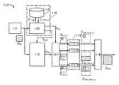
- FIG. 1A is a block diagram of the display device 100.
- FIG. 1B is a view showing a schematic view of the display device 100. As shown in FIG.
- FIG. 1A components are classified according to functions and block diagrams are shown as blocks independent of each other. However, it is difficult to completely divide actual components according to functions, and one component May be associated with multiple functions, or one function may be associated with multiple components.
- the display device 100 includes an image processing device 110 and a display unit 130.
- the image processing apparatus 110 includes an image data input unit 111, an image analysis unit 112, an image division unit 113, a switching circuit 114, an image operation processing unit 115, and an image synthesis unit 116.
- the image operation processing unit 115 includes a plurality of super resolution processing circuits 117 (super resolution processing circuits 117_1 to 117_n (n is a natural number of 2 or more)).
- the image processing apparatus 110 receives image data D IN which is a low resolution video source.
- the image processing apparatus 110 has a function of converting the image data D IN into image data D OUT which is a high resolution video source and outputting it. That is, the image processing apparatus 110 is an apparatus that outputs image data D OUT obtained by up-converting the image data D IN .
- the circuits included in the image processing apparatus 110 is an integrated circuit provided on the printed wiring board 132.
- the image data D IN is input from the input terminal 133, converted into the image data D OUT up-converted by the image processing apparatus 110, and then output to the display unit 130.
- the display unit 130 has a pixel unit 131.
- the pixel portion 131 includes a pixel including a display element and a transistor.
- the display element is preferably a liquid crystal element or a light emitting element.
- the transistor is preferably a bottom gate transistor.
- the semiconductor layer of the transistor preferably contains amorphous silicon.
- the number of masks can be reduced.
- amorphous silicon as the semiconductor layer of the transistor, a manufacturing method of fabricating the transistor on a large substrate can be employed. Therefore, a display device with high mass productivity and capable of increasing the area of the display portion can be provided.
- the image data input to the display unit 130 is the image data D OUT up-converted by the image processing apparatus 110. Therefore, the pixel portion 131 has 7600 or more pixels arranged in the row direction, 4300 or more pixels in the column direction, and has a diagonal of 60 inches or more.
- a high quality display device can be provided.
- a liquid crystal element as a display element
- a thin display device can be achieved, which is preferable.
- a light-emitting element as a display element, a display device with high display quality such as an increase in contrast ratio can be obtained.
- the image data input unit 111 has a function of holding image data D IN input from the outside.
- volatile storage elements such as DRAM (Dynamic RAM) and SRAM (Static RAM) can be applied.
- the image data input unit 111 may have a function such as decoding when the image data D IN is compressed data.
- the image data input unit 111 may have a function of converting the image data D IN into a predetermined format.
- the image data input unit 111 can be omitted.
- the image analysis unit 112 has a function of acquiring information of a target block in an image displayed based on the image data D IN .
- the image analysis unit 112 also has a function of outputting, in the image division unit 113, a control signal S DIV for performing control to divide the image data D IN for each target block.
- the image analysis unit 112 performs different super-resolution processing of any one of the divided image data (image data D DIV , or image data D DIV_1 to image data D DIV n (N is a natural number of 2 or more)). having a plurality of functions of outputting a control signal S UC for controlling the input to the super-resolution processing circuit 117_1 to any one of the super-resolution processing circuit 117_n performed.
- the target block refers to a subject in an image displayed based on the image data D IN , a specific area in the image, and the like. Specifically, it refers to a person, a vehicle, or a landscape.
- the extraction of the target block can be performed by calculating the local feature amount based on the motion vector obtained by comparing the images between a plurality of frames and the data of each pixel in the image data.
- the image data D IN may be input to a neural network circuit, and image recognition may be performed to obtain information of a target block.
- the image analysis unit 112 generates a control signal S DIV for dividing the image data D IN based on information of the target block (hereinafter referred to as target block data D TBIN ).
- the control signal S DIV is output to the image dividing unit 113.
- the plurality of divided image data D DIV generated by the image division unit 113 can be made to be image data D DIV including different target blocks under control of the control signal S DIV .
- control signal S UC for selecting an upconversion algorithm to be applied to the image data D DIV including the image of the target block based on the target block data D TBIN .
- Control signal S UC to the any one of the divided image data D DIV_1 to image data D DIV_n, for selecting whether to apply the algorithm of any up-conversion, a plurality of performing different super-resolution processing
- the input to any one of the super resolution processing circuit 117_1 to the super resolution processing circuit 117_N is controlled.
- Selection algorithm upconverted for the image data D DIV is carried out based on the target block data D TBOUT obtained based on the target block data D TBIN.
- the target block data D TBOUT is output differently for each image of the target block, which is a specific area in the subject or image. For example, an upconversion algorithm that results in a low quality image is applied to image data including a target block such as a vehicle moving at high speed. On the contrary, to image data including target blocks such as a person moving at a low speed, an up-conversion algorithm that results in a high-quality image is applied so as to look natural.
- Image data including a target block moving at a low speed is viewed as if the display quality is extremely degraded when an upconversion algorithm that results in a low quality image is applied.
- image data including a target block moving at high speed is displayed as compared with the case where the upconversion algorithm is used for the high quality image when the upconversion algorithm for the low quality image is applied.
- the grade does not drop extremely. That is, the display device according to one embodiment of the present invention does not apply an upconversion algorithm for uniformly high quality images to image data, but changes an algorithm used for upconversion for each piece of image data including a target block. can do. Therefore, the display device of one embodiment of the present invention can improve the display quality and shorten the processing time of the up conversion of the image data.
- the nearest neighbor algorithm Bilinear method, Bicubic method, Lanczos method, RAISR method, ANR method, A + method, or SRCNN method can be mentioned as an algorithm used for up conversion.
- the above-described low-quality up-conversion algorithm there are the nearest neighbor method, the bilinear method, and the bicubic method.
- RAISR Rapid and Accurate Image Super-Resolution
- ANR Anchored Neighborhood Regression
- a + method As an algorithm for performing high-quality up-conversion as described above, there is a SRCNN (Super-Resolution Convolutional Neural Network) method.
- the image analysis unit 112 includes a signal generation unit 120 and a neural network circuit 118.
- the neural network circuit 118 is a circuit that obtains target block data DTOUT using the target block data DTBIN as input data. Neural network circuit 118, as algorithm for up-conversion corresponding to the target block is obtained, the weighting coefficients of the learned to be capable of outputting the target block data D TBOUT to the input of the target block data D TBIN is stored There is.
- the signal generation unit 120 extracts the target block by calculating the feature amount based on the motion vector obtained by comparing the images between a plurality of frames and the data of each pixel in the image data, and the target block data Generate D TBIN . And the resulting target block data D TBIN to obtain a target block data D TBOUT from the neural network circuit 118 on the basis of a control signal S UC to select the algorithm for up-conversion corresponding to the target block of the image data D IN It can be output.
- the image dividing unit 113 has a function of dividing the image data D IN into a plurality of pieces in accordance with the control signal S DIV .
- the plurality of divided image data D DIV are output to the switching circuit 114.
- the switching circuit 114 has a function of distributing the input image data D DIV to any one of the super-resolution processing circuit 117 _ 1 to the super-resolution processing circuit 117 _ n according to the control signal S UC selecting the upconversion algorithm. .
- image data D DIV image data input to the super-resolution processing circuit 117_1 is illustrated as image data D DIV _ 1 .
- image data D DIV image data input to the super-resolution processing circuit 117_2 is illustrated as image data D DIV_2 .
- image data D DIV image data input to the super-resolution processing circuit 117 _n is illustrated as image data D DIV _ n .
- the image calculation processing unit 115 is a circuit including a plurality of super resolution processing circuits 117_1 to 117_n.
- the super-resolution processing circuits 117_1 to 117_n are circuits that can be up-converted by different algorithms.
- the super resolution processing circuit 117_1 is a circuit that up-converts according to an algorithm of one of the nearest neighbor method, the Bilinear method, the Bicubic method, the Lanczos method, the RAISR method, the ANR method, the A + method, or the SRCNN method.
- the super-resolution processing circuit 117_2 is a circuit that up-converts with an algorithm different from the super-resolution processing circuit 117_1.
- Super-resolution processing circuit 117_1 through 117_n converts the image data obtained by up-converting the image data D DIV_1 to image data D DIV_n (sometimes illustrated with the image data D DIV_1 * UC_1 to image data D DIV_n * UC_n) , Output to the image combining unit 116.
- the image combining unit 116 combines a plurality of pieces of image data up-converted by different algorithms, and outputs the image data D OUT obtained by the up-conversion of the image data D IN to the display unit 130.
- FIG. 1 and 2 illustrate the configuration in which the image data divided using the switching circuit 114 is input to the super-resolution processing circuit that performs up-conversion using an appropriate algorithm, but other configurations may be used. .
- FIG. 3A illustrates a configuration in which a plurality of super resolution processing circuits 119 are provided in the image calculation processing unit 115.
- the super resolution processing circuit 119 receives any one of the image data D DIV _ 1 to D DIV _ n divided by the image division unit 113 and the control signal S UC .
- the super resolution processing circuit 119 is upped by an algorithm of one of the nearest neighbor method, bilinear method, bicubic method, bicubic method, Lanczos method, RAISR method, ANR method, A + method, or SRCNN method according to the input of the control signal S UC. It is a circuit that can be switched to convert. Therefore, any one of the image data D DIV_1 to D DIV n can be up-converted by an algorithm according to the target block.
- FIGS. 1 and 2 has been described as the configuration of generating the target block data DTBIN using the image data D IN input to the image analysis unit 112, other configurations may be used.
- a feature value extraction circuit 122 is provided separately from the signal generation unit 120 and the neural network circuit 118.
- the feature quantity extraction circuit 122 outputs a motion vector obtained by comparing images between a plurality of frames based on the image data D IN, and data D CH including the feature quantity based on data of each pixel in the image data Input to the generation unit 120.
- the signal generation unit 120 can generate the target block data DTBIN based on the image data D IN and the data D CH .
- FIG. 4 is a block diagram of the image processing apparatus 110 shown in FIG. 2 to which a schematic view of an image corresponding to image data is added.
- a hatched square attached together with the image data D IN represents an image based on the original image data.
- hatched rectangles surrounded by broken-line squares, which are added together with the image data D DIV _ 1 to D DIV _ 3 represent an image based on the image data divided for each target block.
- hatched rectangles surrounded by broken-line squares added together with image data D DIV _1 * UC _ 1 to D DIV s 3 * UC _3 are image data up-converted by different algorithms in super resolution processing circuits 117 _ 1 to 117 _ 3.
- the hatched squares attached together with the image data D OUT represent an image based on the up-converted image data.
- an image based on the up-converted image data is illustrated larger than an image based on the image data before up-converted.
- the display device does not apply an upconversion algorithm for uniformly high quality images to image data, but performs upconversion for each image data including a target block.
- An algorithm used can be changed. Therefore, the display device of one embodiment of the present invention can improve the display quality and shorten the processing time of the up conversion of the image data.
- FIG. 5 is a flowchart for explaining the operation of the image processing apparatus 110, focusing on the image analysis unit 112.
- the image data D IN is input (step S01).
- step S02 analysis of the image data D IN is performed (step S02).
- identification of a target block that is, detection of a target block V11 is performed.
- control signal S DIV for dividing the image data for each target block is output to the image dividing unit 113 (step S03).
- the division V12 of the image data is performed by step S03.
- step S04 data DTBIN of the target block for selecting an upconversion algorithm to be applied to each target block is output to the neural network circuit 118 (step S04).
- target block data D TBOUT relating to the upconversion algorithm corresponding to the target block is input from the neural network circuit 118 (step S05).
- step S06 a control signal SUC for selecting an upconversion algorithm to be applied to the divided image data is output to the switching circuit 114 (step S06).
- step S06 selection V14 of an algorithm to be applied to the divided image data is performed.
- FIG. 6 illustrates an image displayed based on the image data D IN in order to explain a specific operation example.
- FIG. 6 (A) illustrates, as an image displayed based on image data, a pedestrian walking near a standing tree along a planted road on which the vehicle travels. Note that FIG. 6A is drawn with a thin line in order to illustrate that the image is a low resolution image before up-conversion.
- FIG. 6A standing trees, pedestrians, vehicles, planting, etc. are illustrated, and in such a case, standing trees, pedestrians in a region surrounded by an alternate long and short dash line in FIG. 6B as a target block.
- Vehicles, and planting are extracted as target blocks, and can be divided into five, such as a roadway and a sidewalk, as other configurations. That is, the image data D IN can be divided into five image data D DIV _ 1 to D DIV _ 5 illustrated in FIGS. 6 (C- 1) to (C- 5). That is, the image analysis unit 112 in FIG. 1 outputs the control signal D DIV so as to be divided into five image data in (C-1) to (C-5) in FIG.
- FIG. 6 (C-2) of FIG. 6 is a vehicle and is a target block that moves at high speed. Therefore, as described above, an upconversion algorithm that results in a low quality image is applied.
- FIG. 6 (C-4) is a pedestrian among FIG. 6 (C-1) thru
- FIG. 6 (C-1) to (C-5) FIG. 6 (C-1), (C-3) and (C-5) are stationary target blocks. In this case, it is sufficient to apply an upconversion algorithm that results in a high quality or low quality image.
- the upconversion algorithm for high quality images is applied to FIG. 6C-3, and the upconversion algorithm for low quality images is applied to FIGS. 6C-1 and 6C-5.
- the image analysis unit 112 in FIG. 1 outputs the control signal S UC so that the above-described up-conversion algorithm is applied to the five image data in (C-1) to (C-5) in FIG. .
- the image data D DIV_1 to D DIV_5 perform up conversion according to the algorithm. It is input to any one of the super resolution processing circuits 117_1 to 117_5 (see FIG. 6D).
- FIG. 6D the fact that the image has been upconverted to a high quality image is drawn with a thick line, and the fact that the image has been upconverted to a low quality image is drawn with a thin line.
- the up-converted image data D DIV_1 * UC_1 to the image data D DIV_5 * UC_5 output from the super-resolution processing circuits 117_1 to 117_5 are synthesized to obtain the up-converted image data D OUT (see FIG. 6D). ).
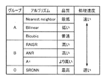
- FIG. 7 shows an example of an algorithm for performing up-conversion.
- each algorithm is classified into groups A, B, or C.
- Group A is an algorithm that performs upconversion by simple calculation
- group B is an algorithm that performs upconversion by machine learning
- group C is an algorithm that performs upconversion by deep learning using a neural network.
- the nearest neighbor method, the bilinear method, and the bicubic method are shown as the group A.
- group B a rapid and accurate image super-resolution (RAISR) method, an anchored proximity regression (ANR) method, and an A + method are shown.
- group C a SRCNN (Super-Resolution Convolutional Neural Network) method is shown.
- the image quality after up conversion is the worst for the nearest neighbor method and the best for the SRCNN method.
- FIG. 7 shows the permutation of the image quality and processing speed obtained by each algorithm when the image quality obtained by the nearest neighbor method is “minimum” and the image quality obtained by the SRCNN method is “high”. .
- the better the image quality after up-conversion the slower the processing speed.
- the up-conversion method using a neural network of a plurality of layers, such as the SRCNN method high-quality images can be obtained, but the processing time becomes long.
- the processing time for upconversion can be shortened by changing the algorithm used for upconversion corresponding to the target block of the image data D IN . Also, the user can view high-quality images with high resolution.
- the neural network circuit 118 preferably has a configuration in which weighting coefficients (weight data) are updated by learning in advance so that target block data DTBOUT corresponding to the target block data DTBIN to be input can be output.
- a learning neural network apparatus 140 is prepared separately from the neural network circuit 118. Then, a large number of image data 145 is prepared in the database 141, target block data DTBIN is extracted from the image data 145, and a data set 142 to which a label of the target block data DTOUT is attached is prepared. The data set 142 is input as training data 143 to the learning neural network circuit 144, and the weight data 146 in the learning neural network circuit 144 is updated.
- Weight data 146 obtained by the learning neural network circuit 144 illustrated in FIG. 8A is weight data 146 in the neural network circuit 118 illustrated in FIG. 2 and the like as illustrated in FIG. 8B. .
- the neural network circuit 118 given the learned weight data 146 can obtain the set target block data D TBOUT as the output data OUT by giving the target block data D TBIN as the input data IN.
- the neural network circuit 118 has an input layer IL, an intermediate layer HL1 (hidden layer), an intermediate layer HL2 (hidden layer), and an output layer OL.
- a hierarchical neural network circuit 118 is configured by the input layer IL, the intermediate layer HL1, the intermediate layer HL2, and the output layer OL.
- the intermediate layer HL1 and the intermediate layer HL2 have an arbitrary number of nodes.
- the middle layer is not limited to two layers. The number of intermediate layers may be one, or three or more.
- the target block data D TBIN is input to the input layer IL, and the weighted information is input to the intermediate layer HL1.
- the information input to the intermediate layer HL1 is weighted by the synapse layer 151 and input to the intermediate layer HL2.
- the information input to the intermediate layer HL2 is weighted by the synapse layer 151 and input to the output layer OL.
- target block data D TBOUT is output from the output layer OL.
- the neural network circuit 118 is configured to increase the number of neurons as the hierarchy advances. That is, the number of neurons in the intermediate layer HL1 is larger than the number of neurons in the input layer IL, and the number of neurons in the intermediate layer HL2 is larger than the number of neurons in the intermediate layer HL1. Further, the number of neurons in the output layer OL is larger than the number of neurons in the intermediate layer HL2. In FIG. 8C, the number of neurons is indicated by the number of arrows connecting the layers. By the number of neurons is configured to increase each time the neural network circuit 118 is hierarchical advances, based on the target block data D TBIN, it is possible to generate the target block data D TBOUT.
- a hierarchical neural network can be fully coupled between each layer or can be partially coupled between each layer.
- a configuration using a convolution layer or a pooling layer can be used between each layer.
- the algorithm used for up-conversion is changed for each image data including a target block. It can be done. Therefore, the display device of one embodiment of the present invention can improve the display quality and shorten the processing time of the up conversion of the image data. Further, according to one embodiment of the present invention, the amount of calculation when applying the upconversion algorithm can be reduced, so power consumption can be reduced.
- This embodiment can be implemented in appropriate combination with the structures described in the other embodiments and the like.
- a configuration example of the display portion 130 using a liquid crystal element as a display element and a configuration example of the display portion 130 using an EL element as a display element are described.
- a sealant 4005 is provided so as to surround the pixel portion 131 provided over the first substrate 4001, and the pixel portion 131 is sealed with the sealant 4005 and the second substrate 4006. .
- the data driver 211a, the data driver 211b, the gate driver 212a, and the gate driver 212b each include a plurality of integrated circuits 4042 provided over a print substrate 4041.
- the integrated circuit 4042 is formed of a single crystal semiconductor or a polycrystalline semiconductor.
- the integrated circuit 4042 included in the gate driver 212 a and the gate driver 212 b has a function of supplying a selection signal to the pixel portion 131.
- the integrated circuit 4042 included in the data driver 211 a and the data driver 211 b has a function of supplying a video signal to the pixel portion 131.
- the integrated circuit 4042 is mounted in a region different from a region surrounded by the sealant 4005 on the first substrate 4001 by a TAB (Tape Automated Bonding) method.
- connection method of the integrated circuit 4042 is not particularly limited, and wire bonding, COG (chip on glass), TCP (tape carrier package), COF (chip on film), or the like may be used. it can.
- FIG. 9B illustrates an example in which the integrated circuit 4042 included in the data driver 211a and the data driver 211b is mounted by a COG method.
- FIG. 9B illustrates an example in which the gate driver 212 a and the gate driver 212 b are formed over the same substrate as the pixel portion 131.
- the driver circuit By forming the driver circuit at the same time as a transistor included in a pixel in the pixel portion 131, the number of components can be reduced. Thus, the productivity can be improved.
- a sealing material 4005 is provided so as to surround the pixel portion 131 provided over the first substrate 4001 and the gate driver 212 a and the gate driver 212 b.
- a second substrate 4006 is provided over the pixel portion 131, the gate driver 212a, and the gate driver 212b.
- FIG. 9B illustrates an example in which the data driver 211 a and the data driver 211 b are separately formed and mounted on the first substrate 4001, the present invention is not limited to this configuration.
- the gate driver may be separately formed and mounted, or part of the data driver or part of the gate driver may be separately formed and mounted.
- the pixel portion 131 may include a panel in which the display element is sealed and a module in which an IC or the like including a controller is mounted on the panel.
- the display portion and the gate driver provided over the first substrate each include a plurality of transistors.
- the structures of the transistors included in the peripheral drive circuit and the transistors included in the pixels of the pixel portion 131 may be the same or different.
- the transistors included in the peripheral drive circuit may all have the same structure, or two or more types of structures may be used in combination.
- transistors included in a pixel may all have the same structure, or two or more types of structures may be used in combination.
- the pixel portion 131 which can be displayed with a resolution of so-called full high definition (also called “2K resolution”, “2K1K”, “2K”, etc.) is realized. can do.
- a pixel portion 131 capable of display at a resolution of so-called ultra high vision also referred to as “4K resolution”, “4K2K”, “4K”, etc.
- ultra high vision also referred to as “4K resolution”, “4K2K”, “4K”, etc.
- a pixel portion 131 capable of display at a resolution of so-called super high vision (also referred to as “8K resolution”, “8K4K”, “8K”, etc.) is realized. be able to.
- 8K resolution also referred to as “8K resolution”, “8K4K”, “8K”, etc.
- the pixels are arranged in a matrix in the pixel unit 131.
- 8K resolution 7600 or more pixels are provided in the row direction, and 4300 or more pixels are provided in the column direction.
- 7680 pixels are provided in the row direction, and 4320 pixels are provided in the column direction.
- FIG. 10A and FIG. 10B are cross-sectional views of a portion indicated by a dashed line of N1-N2 in FIG. 9B.
- the pixel portion 131 illustrated in FIGS. 10A and 10B includes an electrode 4015, and the electrode 4015 is electrically connected to a terminal included in the FPC 4018 through an anisotropic conductive layer 4019. .
- the electrode 4015 is electrically connected to the wiring 4014 in an opening formed in the insulating layer 4112, the insulating layer 4111, and the insulating layer 4110.
- the electrode 4015 is formed of the same conductive layer as the first electrode layer 4030, and the wiring 4014 is formed of the same conductive layer as the source electrode and the drain electrode of the transistor 4010 and the transistor 4011.
- the pixel portion 131 and the gate driver 212 a provided over the first substrate 4001 have a plurality of transistors, and in FIGS. 10A and 10B, the transistors included in the pixel portion 131 are included. 4010 and a transistor 4011 included in the gate driver 212a are illustrated. Note that in FIGS. 10A and 10B, bottom gate transistors are illustrated as the transistor 4010 and the transistor 4011.
- the insulating layer 4112 is provided over the transistor 4010 and the transistor 4011.
- the partition 4510 is formed over the insulating layer 4112.
- the transistor 4010 and the transistor 4011 are provided over the insulating layer 4102.
- the transistor 4010 and the transistor 4011 each include an electrode 4017 formed over the insulating layer 4111.
- the electrode 4017 can function as a back gate electrode.
- the pixel portion 131 illustrated in FIGS. 10A and 10B includes a capacitor 4020.
- the capacitor 4020 includes an electrode 4021 formed in the same step as the gate electrode of the transistor 4010, and an electrode formed in the same step as the source electrode and the drain electrode. The respective electrodes overlap with each other through the insulating layer 4103.
- the capacitance of the capacitor provided in the pixel portion 131 is set so as to be able to hold a charge for a predetermined period, in consideration of the leak current of the transistor and the like.
- the capacitance of the capacitor may be set in consideration of the off current of the transistor and the like.
- FIG. 10A illustrates an example of the pixel portion 131 in which a liquid crystal element is used as a display element.
- a liquid crystal element 4013 which is a display element includes a first electrode layer 4030, a second electrode layer 4031, and a liquid crystal layer 4008.
- an insulating layer 4032 and an insulating layer 4033 which function as alignment films are provided so as to sandwich the liquid crystal layer 4008.
- the second electrode layer 4031 is provided on the second substrate 4006 side, and the first electrode layer 4030 and the second electrode layer 4031 overlap with each other through the liquid crystal layer 4008.
- the spacer 4035 is a columnar spacer obtained by selectively etching the insulating layer, and is provided to control the distance (cell gap) between the first electrode layer 4030 and the second electrode layer 4031. There is. A spherical spacer may be used.
- an optical member such as a black matrix (light shielding layer), a colored layer (color filter), a polarizing member, a retardation member, and an antireflective member may be provided as appropriate.
- an optical member such as a black matrix (light shielding layer), a colored layer (color filter), a polarizing member, a retardation member, and an antireflective member
- circular polarization by a polarization substrate and a retardation substrate may be used.
- a backlight, a sidelight, or the like may be used as a light source.
- a light-shielding layer 4132, a coloring layer 4131, and an insulating layer 4133 are provided between the substrate 4006 and the second electrode layer 4031.
- the material that can be used as the light shielding layer examples include carbon black, titanium black, metals, metal oxides, and composite oxides containing a solid solution of a plurality of metal oxides.
- the light shielding layer may be a film containing a resin material or a thin film of an inorganic material such as metal.
- a stacked film of films including a material of a colored layer can also be used for the light shielding layer.
- a layered structure of a film containing a material used for a colored layer transmitting light of a certain color and a film containing a material used for a colored layer transmitting light of another color can be used. It is preferable to use a common material for the colored layer and the light shielding layer, as it is possible to share the device and simplify the process.
- Materials usable for the colored layer include metal materials, resin materials, resin materials containing pigments or dyes, and the like.
- the formation method of the light shielding layer and the colored layer may be performed in the same manner as the formation method of each layer described above. For example, it may be performed by an inkjet method.
- the pixel portion 131 illustrated in FIGS. 10A and 10B includes the insulating layer 4111 and the insulating layer 4103.
- As the insulating layer 4111 and the insulating layer 4103 an insulating layer which hardly transmits an impurity element is used. By sandwiching the semiconductor layer of the transistor between the insulating layer 4111 and the insulating layer 4103, entry of impurities from the outside can be prevented.
- a light-emitting element (also referred to as “EL element”) using electroluminescence can be applied.
- the EL element has a layer containing a light-emitting compound (also referred to as “EL layer”) between a pair of electrodes.
- EL layer a light-emitting compound
- EL elements are distinguished depending on whether the light emitting material is an organic compound or an inorganic compound, and in general, the former is called an organic EL element and the latter is called an inorganic EL element.
- the organic EL element In the organic EL element, electrons are injected from one electrode and holes are injected from the other electrode to the EL layer by applying a voltage. Then, the carriers (electrons and holes) recombine to form an excited state of the light emitting organic compound, and light is emitted when the excited state returns to the ground state. From such a mechanism, such a light emitting element is referred to as a current excitation light emitting element.
- the EL layer is a substance having a high hole injection property, a substance having a high hole transport property, a hole blocking material, a substance having a high electron transport property, a substance having a high electron injection property, or a bipolar other than a light emitting compound. It may have a polar substance (a substance having a high electron transporting property and a hole transporting property) or the like.
- the EL layer can be formed by an evaporation method (including a vacuum evaporation method), a transfer method, a printing method, an inkjet method, a coating method, or the like.
- Inorganic EL elements are classified into a dispersion-type inorganic EL element and a thin-film-type inorganic EL element according to the element configuration.
- the dispersion-type inorganic EL element has a light-emitting layer in which particles of a light-emitting material are dispersed in a binder, and the light emission mechanism is donor-acceptor recombination light emission utilizing a donor level and an acceptor level.
- the thin film type inorganic EL element has a structure in which the light emitting layer is sandwiched by dielectric layers and further sandwiched by electrodes, and the light emission mechanism is localized light emission utilizing inner shell electron transition of metal ions.
- an organic EL element is described as a light emitting element.
- one of at least a pair of electrodes may be transparent in order to extract light emission.
- a transistor and a light emitting element are formed over the substrate, and top emission (top emission) structure in which light emission is extracted from the surface opposite to the substrate, or bottom emission (bottom emission) structure in which light emission is extracted from the surface of the substrate.
- top emission (top emission) structure in which light emission is extracted from the surface opposite to the substrate
- bottom emission (bottom emission) structure in which light emission is extracted from the surface of the substrate
- FIG. 10B is an example of the pixel portion 131 using a light emitting element as a display element.
- a light emitting element 4513 which is a display element is electrically connected to the transistor 4010 provided in the pixel portion 131.
- the structure of the light-emitting element 4513 is a stacked structure of the first electrode layer 4030, the light-emitting layer 4511, and the second electrode layer 4031, but is not limited to this structure.
- the structure of the light emitting element 4513 can be changed as appropriate in accordance with the direction of light extracted from the light emitting element 4513 or the like.
- the partition 4510 is formed using an organic insulating material or an inorganic insulating material.
- the light-emitting layer 4511 may be either a single layer or a plurality of stacked layers.
- the emission color of the light-emitting element 4513 can be changed to white, red, green, blue, cyan, magenta, yellow, or the like depending on the material of the light-emitting layer 4511.
- a method of realizing color display there are a method of combining a light emitting element 4513 of white light emitting color and a coloring layer, and a method of providing a light emitting element 4513 of different light emitting color for each pixel.
- the former method is more productive than the latter method.
- the productivity is lower than the former method.
- luminescent color having higher color purity can be obtained than in the former method.
- the color purity can be further enhanced by providing the light emitting element 4513 with a microcavity structure.
- the light emitting layer 4511 may have an inorganic compound such as a quantum dot.
- a quantum dot for the light-emitting layer, it can also function as a light-emitting material.
- a protective layer may be formed over the second electrode layer 4031 and the partition 4510 so that oxygen, hydrogen, moisture, carbon dioxide, and the like do not enter the light-emitting element 4513.
- the protective layer silicon nitride, silicon nitride oxide, aluminum oxide, aluminum nitride, aluminum oxynitride, aluminum nitride oxide, DLC (Diamond Like Carbon), or the like can be formed.
- a filler 4514 is provided in a space sealed by the first substrate 4001, the second substrate 4006, and the sealant 4005 and sealed.
- a protective film such as a laminated film or an ultraviolet curable resin film
- a cover material which has high airtightness and low degassing so as not to be exposed to the outside air.
- an ultraviolet curable resin or a thermosetting resin in addition to an inert gas such as nitrogen or argon, an ultraviolet curable resin or a thermosetting resin can be used, and PVC (polyvinyl chloride), acrylic resin, polyimide, epoxy resin, silicone resin, PVB ( Polyvinyl butyral) or EVA (ethylene vinyl acetate) etc. can be used.
- the filler 4514 may contain a desiccant.
- sealant 4005 a glass material such as a glass frit, a cured resin such as a two-component mixed resin that cures at normal temperature, a photocurable resin, or a thermosetting resin can be used.
- the sealant 4005 may contain a desiccant.
- an optical film such as a polarizing plate or a circularly polarizing plate (including an elliptically polarizing plate), a retardation plate ( ⁇ / 4 plate, ⁇ / 2 plate), or a color filter may be provided on the emission surface of the light emitting element. You may provide suitably.
- an antireflective film may be provided on the polarizing plate or the circularly polarizing plate. For example, anti-glare processing can be performed to diffuse reflected light and reduce reflection due to the unevenness of the surface.
- light with high color purity can be extracted by forming the light-emitting element with a microcavity structure.
- reflection can be reduced, and the visibility of a display image can be enhanced.
- first electrode layer and the second electrode layer (also referred to as a pixel electrode layer, a common electrode layer, a counter electrode layer, and the like) which apply voltage to the display element, the direction of light to be extracted, the location where the electrode layer is provided, and Translucency and reflectivity may be selected depending on the pattern structure of the electrode layer.
- the first electrode layer 4030 and the second electrode layer 403 are indium oxide containing tungsten oxide, indium zinc oxide containing tungsten oxide, indium oxide containing titanium oxide, indium tin oxide, indium containing titanium oxide
- a light-transmitting conductive material such as tin oxide, indium zinc oxide, or indium tin oxide to which silicon oxide is added can be used.
- the first electrode layer 4030 and the second electrode layer 4031 are made of tungsten (W), molybdenum (Mo), zirconium (Zr), hafnium (Hf), vanadium (V), niobium (Nb), tantalum (Ta) , Chromium (Cr), cobalt (Co), nickel (Ni), titanium (Ti), platinum (Pt), aluminum (Al), copper (Cu), metals such as silver (Ag), or alloys thereof, or It can be formed using one or more of metal nitrides.
- the first electrode layer 4030 and the second electrode layer 4031 can be formed using a conductive composition containing a conductive high molecule (also referred to as a conductive polymer).
- a conductive high molecule also referred to as a conductive polymer.
- a so-called ⁇ electron conjugated conductive high molecule can be used.
- polyaniline or a derivative thereof, polypyrrole or a derivative thereof, polythiophene or a derivative thereof, or a copolymer of two or more of aniline, pyrrole and thiophene or a derivative thereof can be given.
- a protective circuit for protecting the driver circuit is preferably provided.
- the protection circuit is preferably configured using a non-linear element.
- This embodiment can be implemented in appropriate combination with the structures described in the other embodiments and the like.
- the display portion 130 and the like of one embodiment of the present invention can be manufactured using various types of transistors such as a bottom gate transistor and a top gate transistor.
- transistors such as a bottom gate transistor and a top gate transistor.
- a planar transistor or a staggered transistor may be used. Therefore, according to the existing manufacturing line, the material of the semiconductor layer to be used and the transistor structure can be easily replaced.
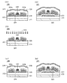
- FIG. 11A1 is a cross-sectional view of a channel protective transistor 310 which is a kind of bottom gate transistor.
- the transistor 310 is formed over a substrate 371.
- the transistor 310 includes an electrode 322 over the substrate 371 with the insulating layer 372 interposed therebetween.
- the semiconductor layer 324 is provided over the electrode 322 with the insulating layer 326 interposed therebetween.
- the electrode 322 can function as a gate electrode.
- the insulating layer 326 can function as a gate insulating layer.
- the insulating layer 327 is provided over the channel formation region of the semiconductor layer 324.
- an electrode 344 a and an electrode 344 b are provided over the insulating layer 326 in contact with part of the semiconductor layer 324.
- the electrode 344a can function as one of a source electrode and a drain electrode.
- the electrode 344 b can function as the other of the source electrode and the drain electrode.
- a portion of the electrode 344 a and a portion of the electrode 344 b are formed over the insulating layer 327.
- the insulating layer 327 can function as a channel protective layer. By providing the insulating layer 327 over the channel formation region, exposure of the semiconductor layer 324 which is generated at the time of formation of the electrodes 344a and 344b can be prevented. Thus, the channel formation region of the semiconductor layer 324 can be prevented from being etched when the electrode 344a and the electrode 344b are formed.
- the transistor 310 includes the insulating layer 328 over the electrode 344 a, the electrode 344 b, and the insulating layer 327, and the insulating layer 329 over the insulating layer 328.
- a layer functioning as an n-type semiconductor or a p-type semiconductor is preferably provided between the semiconductor layer 324 and the electrode 344a and between the semiconductor layer 324 and the electrode 344b.
- a layer functioning as an n-type semiconductor or a p-type semiconductor can function as a source region or a drain region of a transistor.
- the insulating layer 329 is preferably formed using a material having a function of preventing or reducing diffusion of impurities into the transistor from the outside. Note that the insulating layer 329 can be omitted as needed.
- a transistor 311 illustrated in FIG. 11A2 is different from the transistor 310 in that the electrode 311 which can function as a back gate electrode is provided over the insulating layer 329.
- the electrode 323 can be formed by the same material and method as the electrode 322.
- the back gate electrode is formed of a conductive layer, and the gate electrode and the back gate electrode are disposed so as to sandwich the channel formation region of the semiconductor layer.
- the back gate electrode can function similarly to the gate electrode.
- the potential of the back gate electrode may be the same as that of the gate electrode, or may be the ground potential (GND potential) or any potential.
- the threshold voltage of the transistor can be changed by changing the potential of the back gate electrode independently without interlocking with the gate electrode.
- the electrode 322 and the electrode 323 can both function as gate electrodes.
- the insulating layer 326, the insulating layer 328, and the insulating layer 329 can each function as a gate insulating layer.
- the electrode 323 may be provided between the insulating layer 328 and the insulating layer 329.
- the other is referred to as a “back gate electrode”.
- the electrode 322 when the electrode 323 is referred to as a “gate electrode”, the electrode 322 is referred to as a “back gate electrode”.
- the transistor 311 can be considered as a kind of top gate transistor.
- one of the electrode 322 and the electrode 323 may be referred to as “first gate electrode”, and the other may be referred to as “second gate electrode”.
- the region where carriers flow in the semiconductor layer 324 becomes larger in the film thickness direction.
- the amount of carrier movement increases.
- the on-state current of the transistor 311 is increased and the field-effect mobility is increased.
- the transistor 311 is a transistor having a large on current with respect to the occupied area. That is, the occupied area of the transistor 311 can be reduced with respect to the required on current.
- the gate electrode and the back gate electrode are formed of a conductive layer, they have a function to prevent an electric field generated outside the transistor from acting on the semiconductor layer in which a channel is formed (in particular, an electric field shielding function against static electricity). .
- the electric field shielding function can be enhanced by forming the back gate electrode larger than the semiconductor layer and covering the semiconductor layer with the back gate electrode.
- Each of the gate electrode and the back gate electrode has a function of shielding an external electric field, so that charges such as charged particles generated above and below the transistor do not affect the channel formation region of the semiconductor layer.
- a stress test for example, a negative gate bias-temperature (NGBT) test in which a negative voltage is applied to a gate (also referred to as “NBT” or “NBTS”) is suppressed.
- NBT negative gate bias-temperature
- NBTS negative voltage bias-temperature
- the back gate electrode can be cut off so that the electric field generated from the drain electrode does not act on the semiconductor layer, which can suppress the variation of the rising voltage of the on current due to the variation of the drain voltage. This effect is remarkable when the potential is supplied to the gate electrode and the back gate electrode.
- PBT positive gate bias-temperature
- BT stress tests such as NGBT and PGBT are a type of accelerated test and can evaluate in a short time the change in characteristics (change over time) of the transistor caused by long-term use.
- the amount of fluctuation of the threshold voltage of the transistor before and after the BT stress test is an important index for investigating the reliability. Before and after the BT stress test, it can be said that the smaller the amount of fluctuation of the threshold voltage, the higher the reliability of the transistor.
- FIG. 11B1 is a cross-sectional view of a channel protective transistor 320 which is one of bottom-gate transistors.
- the transistor 320 has substantially the same structure as the transistor 310, except that the insulating layer 327 covers the semiconductor layer 324.
- the semiconductor layer 324 and the electrode 344 a are electrically connected to each other in an opening formed by selectively removing part of the insulating layer 327 overlapping with the semiconductor layer 324.
- the semiconductor layer 324 and the electrode 344 b are electrically connected to each other in another opening which is formed by selectively removing a part of the insulating layer 327 overlapping with the semiconductor layer 324.
- the region of the insulating layer 327 overlapping with the channel formation region can function as a channel protective layer.
- a transistor 321 illustrated in FIG. 11B2 is different from the transistor 320 in that the electrode 321 which can function as a back gate electrode is provided over the insulating layer 329.
- the insulating layer 327 can prevent the semiconductor layer 324 from being exposed when the electrodes 344 a and 344 b are formed. Thus, thinning of the semiconductor layer 324 can be prevented at the time of formation of the electrode 344a and the electrode 344b.
- the distance between the electrode 344a and the electrode 322 and the distance between the electrode 344b and the electrode 322 are longer than those in the transistors 310 and 311.
- parasitic capacitance generated between the electrode 344 a and the electrode 322 can be reduced.
- parasitic capacitance generated between the electrode 344 b and the electrode 322 can be reduced.
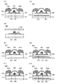
- a transistor 325 illustrated in FIG. 11C1 is a channel etching transistor which is one of bottom-gate transistors.
- the transistor 325 forms the electrode 344a and the electrode 344b without using the insulating layer 327. Therefore, part of the semiconductor layer 324 exposed when the electrodes 344a and 344b are formed may be etched. On the other hand, since the insulating layer 327 is not provided, productivity of the transistor can be increased.
- a transistor 326 illustrated in FIG. 11C2 is different from the transistor 325 in that the electrode 326 which can function as a back gate electrode is provided over the insulating layer 329.
- FIG. 12A1 is a cross-sectional view of a transistor 330 which is a kind of top gate transistor.
- the transistor 330 includes the semiconductor layer 324 over the insulating layer 372, and over the semiconductor layer 324 and the insulating layer 372, an electrode 344a in contact with part of the semiconductor layer 324 and an electrode 344b in contact with part of the semiconductor layer 324. And the insulating layer 326 over the semiconductor layer 324, the electrode 344a, and the electrode 344b, and the electrode 322 over the insulating layer 326.
- the transistor 330 reduces parasitic capacitance generated between the electrode 322 and the electrode 344a and parasitic capacitance generated between the electrode 322 and the electrode 344b because the electrode 322 and the electrode 344a and the electrode 322 and the electrode 344b do not overlap. be able to. Further, after the electrode 322 is formed, the impurity region can be formed in the semiconductor layer 324 in a self-aligned manner (self-alignment) by introducing the impurity 255 into the semiconductor layer 324 using the electrode 322 as a mask. See FIG. 12 (A3)).
- the impurity 255 can be introduced using an ion implantation apparatus, an ion doping apparatus, or a plasma treatment apparatus.
- the impurity 255 for example, at least one element of a Group 13 element or a Group 15 element can be used. In the case where an oxide semiconductor is used for the semiconductor layer 324, at least one element of a rare gas, hydrogen, and nitrogen can also be used as the impurity 255.
- the transistor 331 illustrated in FIG. 12A2 is different from the transistor 330 in that the electrode 323 and the insulating layer 227 are included.
- the transistor 331 includes the electrode 323 formed over the insulating layer 372 and the insulating layer 227 formed over the electrode 323.
- the electrode 323 can function as a back gate electrode.
- the insulating layer 227 can function as a gate insulating layer.
- the insulating layer 227 can be formed by the same material and method as the insulating layer 326.
- the transistor 331 is a transistor having a large on current with respect to an occupied area. That is, the area occupied by the transistor 331 can be reduced with respect to the on current required.
- the transistor 340 illustrated in FIG. 12B1 is one of top-gate transistors.
- the transistor 340 is different from the transistor 330 in that the semiconductor layer 324 is formed after the electrodes 344 a and 344 b are formed.
- the transistor 341 illustrated in FIG. 12B2 is different from the transistor 340 in that the electrode 323 and the insulating layer 227 are included.
- part of the semiconductor layer 324 is formed over the electrode 344a, and the other part of the semiconductor layer 324 is formed over the electrode 344b.
- the transistor 341 is a transistor having a large on current with respect to the occupied area. That is, the occupied area of the transistor 341 can be reduced with respect to the required on current.
- the transistor 342 illustrated in FIG. 13A1 is one of top-gate transistors.
- the transistor 342 differs from the transistor 330 and the transistor 340 in that the electrode 344 a and the electrode 344 b are formed after the insulating layer 329 is formed.
- the electrode 344 a and the electrode 344 b are electrically connected to the semiconductor layer 324 in an opening formed in the insulating layer 328 and the insulating layer 329.
- the transistor 342 has a region where the insulating layer 326 extends beyond the end of the electrode 322.
- the impurity concentration of the region into which the impurity 255 is introduced through the insulating layer 326 of the semiconductor layer 324 is higher than the region into which the impurity 255 is introduced without through the insulating layer 326. It becomes smaller.
- a lightly doped drain (LDD) region is formed in a region which does not overlap with the electrode 322.
- the transistor 343 illustrated in FIG. 13A2 is different from the transistor 342 in that the electrode 323 is provided.
- the transistor 343 includes an electrode 323 formed over the substrate 371 and overlaps with the semiconductor layer 324 with the insulating layer 372 interposed therebetween.
- the electrode 323 can function as a back gate electrode.
- the transistor 344 illustrated in FIG. 13B1 and the transistor 345 illustrated in FIG. 13B2 all the insulating layer 326 in a region which does not overlap with the electrode 322 may be removed.
- the transistor 346 illustrated in FIG. 13C1 and the transistor 347 illustrated in FIG. 13C2 the insulating layer 326 may be left.
- the transistors 342 to 347 can also form impurity regions in the semiconductor layer 324 in a self-aligned manner by introducing the impurity 255 into the semiconductor layer 324 using the electrode 322 as a mask after forming the electrode 322. .
- substrate There is no big limitation in the material used for a substrate. Depending on the purpose, it may be determined in consideration of the presence or absence of light-transmitting property and heat resistance to the extent that it can withstand heat treatment. For example, glass substrates such as barium borosilicate glass and aluminoborosilicate glass, ceramic substrates, quartz substrates, sapphire substrates and the like can be used. In addition, a semiconductor substrate, a flexible substrate (flexible substrate), a bonded film, a base film, or the like may be used.
- glass substrates such as barium borosilicate glass and aluminoborosilicate glass, ceramic substrates, quartz substrates, sapphire substrates and the like can be used.
- a semiconductor substrate, a flexible substrate (flexible substrate), a bonded film, a base film, or the like may be used.
- the semiconductor substrate may be, for example, a semiconductor substrate made of silicon or germanium or a compound semiconductor substrate made of silicon carbide, silicon germanium, gallium arsenide, indium phosphide, zinc oxide or gallium oxide. .
- the semiconductor substrate may be a single crystal semiconductor or a polycrystalline semiconductor.
- the sixth generation (1500 mm ⁇ 1850 mm), the seventh generation (1870 mm ⁇ 2200 mm), the eighth generation (2200 mm ⁇ 2400 mm), the ninth generation (2400 mm ⁇ 2800 mm), the tenth generation (2950 mm ⁇ 3400 mm) Etc.
- the sixth generation (1500 mm ⁇ 1850 mm
- the seventh generation (1870 mm ⁇ 2200 mm
- the eighth generation (2200 mm ⁇ 2400 mm
- the ninth generation (2400 mm ⁇ 2800 mm
- the tenth generation (2950 mm ⁇ 3400 mm) Etc.
- a flexible substrate (flexible substrate), a bonded film, a base film, or the like may be used as a substrate.
- polyester resins such as polyethylene terephthalate (PET) and polyethylene naphthalate (PEN), polyacrylonitrile resin, acrylic resin, polyimide resin, polymethyl methacrylate Resin, polycarbonate (PC) resin, polyether sulfone (PES) resin, polyamide resin (nylon, aramid etc.), polysiloxane resin, cycloolefin resin, polystyrene resin, polyamide imide resin, polyurethane resin, polyvinyl chloride resin, poly chloride A vinylidene resin, a polypropylene resin, a polytetrafluoroethylene (PTFE) resin, an ABS resin, a cellulose nanofiber etc. can be used.
- PET polyethylene terephthalate
- PEN polyethylene naphthalate
- PES polyether sulfone
- polyamide resin nylon, aramid etc.
- polysiloxane resin cycloolefin resin
- polystyrene resin polyamide imide
- a lightweight display device By using the above-described material as a substrate, a lightweight display device can be provided. Further, by using the above-described material as a substrate, a display device resistant to shock can be provided. In addition, by using the above material as a substrate, a display device which is not easily damaged can be provided.
- a flexible substrate used for the substrate for example, a material having a linear expansion coefficient of 1 ⁇ 10 ⁇ 3 / K or less, 5 ⁇ 10 ⁇ 5 / K or less, or 1 ⁇ 10 ⁇ 5 / K or less may be used.
- aramid is suitable as a flexible substrate because of its low coefficient of linear expansion.
- Conductive layer As conductive materials which can be used for conductive layers such as wirings, electrodes, and the like other than the gate, source, and drain of the transistor, aluminum (Al), chromium (Cr), copper (Cu), and silver can be used.
- niobium Metal elements selected from (Nb), manganese (Mn), magnesium (Mg), zirconium (Zr), beryllium (Be), etc., alloys containing the above-mentioned metal elements, or alloys combining the above-mentioned metal elements Etc. can be used.
- a semiconductor typified by polycrystalline silicon containing an impurity element such as phosphorus or a silicide such as nickel silicide may be used.
- the formation method of the conductive material is not particularly limited, and various formation methods such as a vapor deposition method, a CVD method, a sputtering method, and a spin coating method can be used.
- a Cu-X alloy (X is Mn, Ni, Cr, Fe, Co, Mo, Ta, or Ti) may be applied as the conductive material.
- a layer formed of a Cu-X alloy can be processed by a wet etching process, which makes it possible to suppress the manufacturing cost.
- an aluminum alloy containing one or more elements selected from titanium, tantalum, tungsten, molybdenum, chromium, neodymium, and scandium may be used as the conductive material.
- a conductive material which can be used for the conductive layer indium tin oxide, indium oxide containing tungsten oxide, indium zinc oxide containing tungsten oxide, indium oxide containing titanium oxide, indium tin containing titanium oxide
- a conductive material having oxygen, such as oxide, indium zinc oxide, indium tin oxide to which silicon oxide is added, can also be used.
- a conductive material containing nitrogen such as titanium nitride, tantalum nitride, tungsten nitride, or the like can be used.
- the conductive layer can also have a stacked structure in which a conductive material containing oxygen, a conductive material containing nitrogen, and a conductive material containing the above-described metal element are combined as appropriate.
- the conductive layer has a single-layer structure of an aluminum layer containing silicon, a two-layer structure in which a titanium layer is stacked on an aluminum layer, a two-layer structure in which a titanium layer is stacked on a titanium nitride layer, a tungsten layer on a titanium nitride layer
- a two-layer structure in which a tungsten layer is stacked on a tantalum nitride layer a three-layer structure in which a titanium layer and an aluminum layer are stacked on the titanium layer, and a titanium layer is further stacked thereon Good.
- a plurality of conductive layers formed of the above conductive materials may be stacked.
- the conductive layer may have a stacked structure in which the above-described material containing a metal element and the conductive material containing oxygen are combined.
- a stacked structure in which a material containing a metal element described above and a conductive material containing nitrogen are combined may be used.
- a stacked structure in which the above-described material containing a metal element, the conductive material containing oxygen, and the conductive material containing nitrogen are combined may be used.
- a conductive layer is stacked over a conductive layer including at least one of indium or zinc and oxygen, a conductive layer including copper is stacked, and a conductive layer including at least one of indium or zinc and oxygen is further stacked thereon It may be a three-layer structure.
- the side surface of the conductive layer containing copper is also preferably covered with the conductive layer containing oxygen and at least one of indium and zinc.
- a plurality of conductive layers containing oxygen and at least one of indium and zinc may be stacked as the conductive layer.
- Each insulating layer is made of aluminum nitride, aluminum oxide, aluminum nitride oxide, aluminum oxynitride, magnesium oxide, silicon oxide, silicon oxide, silicon nitride oxide, silicon oxynitride, silicon oxynitride, gallium oxide, germanium oxide, yttrium oxide, zirconium oxide, lanthanum oxide
- a material selected from neodymium oxide, hafnium oxide, tantalum oxide, aluminum silicate and the like is used in a single layer or laminated state.
- a material obtained by mixing a plurality of materials among an oxide material, a nitride material, an oxynitride material, and a nitride oxide material may be used.
- the nitrided oxide refers to a compound having a higher content of nitrogen than oxygen.
- oxynitride refers to a compound having a higher content of oxygen than nitrogen.
- the content of each element can be measured, for example, using Rutherford Backscattering Spectroscopy (RBS) or the like.
- the insulating layer 372 and the insulating layer 329 are preferably formed using an insulating material which hardly transmits impurities.
- an insulating material comprising boron, carbon, nitrogen, oxygen, fluorine, magnesium, aluminum, silicon, phosphorus, chlorine, argon, gallium, germanium, yttrium, zirconium, lanthanum, neodymium, hafnium or tantalum, or It may be used in lamination.
- an insulating layer which can function as a planarization layer may be used as the insulating layer.
- a heat-resistant organic material such as polyimide, an acrylic resin, a benzocyclobutene resin, a polyamide, or an epoxy resin can be used.
- low dielectric constant materials low-k materials
- siloxane resins PSG (phosphorus glass), BPSG (phosphorus boron glass), and the like can be used. Note that a plurality of insulating layers formed of these materials may be stacked.
- the siloxane-based resin corresponds to a resin including a Si-O-Si bond formed using a siloxane-based material as a starting material.
- the siloxane-based resin may use an organic group (for example, an alkyl group or an aryl group) or a fluoro group as a substituent.
- the organic group may have a fluoro group.
- CMP treatment may be performed on the surface of the insulating layer or the like.
- CMP treatment unevenness of the sample surface can be reduced and coverage with an insulating layer and a conductive layer to be formed later can be improved.
- semiconductor layer As a semiconductor material used for a semiconductor layer of a transistor, any of an amorphous semiconductor, a semiconductor having crystallinity (a microcrystalline semiconductor, a polycrystalline semiconductor, a single crystal semiconductor, or a semiconductor having a crystalline region in part) can be used. Good.
- silicon, germanium, or the like can be used as a semiconductor material used for the semiconductor layer of the transistor.
- a compound semiconductor such as silicon carbide, gallium arsenide, a metal oxide, or a nitride semiconductor, an organic semiconductor, or the like can be used.
- amorphous silicon can be used as a semiconductor material used for the transistor.
- amorphous silicon is excellent in mass productivity and can be easily provided on a substrate with a large area.
- amorphous silicon used for a transistor contains a large amount of hydrogen. Therefore, amorphous silicon containing a large amount of hydrogen may be referred to as “hydrogenated amorphous silicon” or “a-Si: H”.
- a-Si: H hydrogenated amorphous silicon
- amorphous silicon can be formed at a lower temperature than polycrystalline silicon, the maximum temperature in the manufacturing process can be lowered. Therefore, a material with low heat resistance can be used for the substrate, the conductive layer, the insulating layer, and the like.
- crystalline silicon such as microcrystalline silicon, polycrystalline silicon, single crystal silicon, or the like can be used.
- polycrystalline silicon can be formed at a lower temperature than single crystal silicon, and has high field effect mobility and high reliability as compared to amorphous silicon.
- an oxide semiconductor which is a kind of metal oxide can be used as a semiconductor material used for the transistor.
- an oxide semiconductor containing indium can be used.
- An oxide semiconductor can achieve higher field-effect mobility and higher reliability than amorphous silicon.
- an oxide semiconductor is excellent in mass productivity and can be easily provided over a substrate with a large area.
- an oxide semiconductor which is a kind of metal oxide has a wider band gap and a lower carrier density than silicon, it is preferably used for a semiconductor layer of a transistor. It is preferable to use an oxide semiconductor for the semiconductor layer of the transistor because a current flowing between the source and the drain in the off state of the transistor can be reduced.
- the energy gap of the oxide semiconductor which is a kind of metal oxide is preferably 2 eV or more, more preferably 2.5 eV or more, and still more preferably 3 eV or more. As described above, with the use of the oxide semiconductor with a wide energy gap, the off-state current of the transistor can be reduced.
- An oxide semiconductor which is a kind of metal oxide is, for example, In-M containing at least indium, zinc and M (a metal such as aluminum, titanium, gallium, germanium, yttrium, zirconium, lanthanum, cerium, tin, neodymium or hafnium). It is preferable to contain a material represented by -Zn-based oxide. In addition, in order to reduce variation in electrical characteristics of a transistor including the oxide semiconductor, a stabilizer is preferably included.
- the stabilizer includes, for example, gallium, tin, hafnium, aluminum, or zirconium, including the metals described in M above.
- Other stabilizers include lanthanides such as lanthanum, cerium, praseodymium, neodymium, samarium, europium, gadolinium, terbium, dysprosium, holmium, erbium, thulium, ytterbium, lutetium and the like.
- a metal oxide constituting the semiconductor layer for example, In—Ga—Zn-based oxide, In—Al—Zn-based oxide, In—Sn—Zn-based oxide, In—Hf—Zn-based oxide, In— La-Zn-based oxide, In-Ce-Zn-based oxide, In-Pr-Zn-based oxide, In-Nd-Zn-based oxide, In-Sm-Zn-based oxide, In-Eu-Zn-based oxide In-Gd-Zn-based oxide, In-Tb-Zn-based oxide, In-Dy-Zn-based oxide, In-Ho-Zn-based oxide, In-Er-Zn-based oxide, In-Tm -Zn-based oxide, In-Yb-Zn-based oxide, In-Lu-Zn-based oxide, In-Sn-Ga-Zn-based oxide, In-Hf-Ga-Zn-based oxide, In-Al- Ga-Zn-based oxide, In-Sn-
- an In—Ga—Zn-based oxide means an oxide having In, Ga, and Zn as main components, and there is no limitation on the ratio of In, Ga, and Zn.
- metal elements other than In, Ga, and Zn may be contained.
- An insulating layer, a semiconductor layer, a conductive layer for forming an electrode or a wiring, and the like can be formed by sputtering, chemical vapor deposition (CVD), vacuum evaporation, pulsed laser deposition (PLD) Or atomic layer deposition (ALD) method or the like.
- CVD chemical vapor deposition
- PLAD pulsed laser deposition
- ALD atomic layer deposition
- PECVD plasma chemical vapor deposition
- a thermal CVD method may be used as an example of the thermal CVD method.
- MOCVD Metal Organic CVD
- an insulating layer, a semiconductor layer, a conductive layer for forming an electrode or a wiring, and the like which constitute a display device may be spin-coated, dip, spray-applied, inkjet, dispensing, screen printing, offset printing, slit coating, roll coating, You may form by methods, such as a curtain coat and a knife coat.
- the PECVD method provides high quality films at relatively low temperatures.
- a deposition method such as MOCVD method, ALD method, or thermal CVD method which does not use plasma at the time of deposition
- damage to a formation surface is less likely to occur.
- a wiring, an electrode, an element (such as a transistor or a capacitor), or the like included in a transistor may be charged up by receiving charge from plasma.
- wirings, electrodes, elements, and the like included in the transistor may be broken by the stored charge.
- the film formation method which does not use plasma since the plasma damage does not occur, the yield of the transistor can be increased.
- plasma damage does not occur during film formation, a film with few defects can be obtained.
- the CVD method and the ALD method are film forming methods in which a film is formed by a reaction on the surface of an object to be processed unlike a film forming method in which particles released from a target or the like are deposited. Therefore, the film forming method is less susceptible to the shape of the object to be processed, and has good step coverage.
- the ALD method since the ALD method has excellent step coverage and uniformity of thickness, it is suitable for coating the surface of an opening with a high aspect ratio.
- the ALD method may be preferably used in combination with another deposition method such as a CVD method having a high deposition rate.
- the CVD method and the ALD method can control the composition of the obtained film by the flow rate ratio of the source gas.
- a film having any composition can be formed depending on the flow rate ratio of the source gas.
- a film whose composition is continuously changed can be formed by changing the flow ratio of the source gas while forming the film.
- processing can be performed using a photolithography method or the like.
- the island-shaped layer may be formed by a film formation method using a shielding mask.
- the layer may be processed by a nanoimprint method, a sand blast method, a lift off method, or the like.
- the photolithography method a resist mask is formed on a layer (thin film) to be processed, a part of the layer (thin film) is selectively removed using the resist mask as a mask, and then the resist mask is removed.
- light used for exposure may be, for example, i-ray (wavelength 365 nm), g-ray (wavelength 436 nm), h-ray (wavelength 405 nm), or a mixture of these.
- ultraviolet light, KrF laser light, ArF laser light or the like can also be used.
- the exposure may be performed by the immersion exposure technique.
- extreme ultraviolet (EUV: Extreme Ultra-violet) or X-rays may be used.
- an electron beam can be used instead of light used for exposure. The use of extreme ultraviolet light, X-rays or electron beams is preferable because extremely fine processing is possible. In the case where exposure is performed by scanning a beam such as an electron beam, a photomask is not necessary.
- etching For removal (etching) of the layer (thin film), a dry etching method, a wet etching method, a sand blast method, or the like can be used. In addition, these etching methods may be used in combination.
- This embodiment can be implemented in appropriate combination with the structures described in the other embodiments and the like.
- Embodiment 4 One embodiment of the present invention can be used for various electronic devices having a display portion.
- a display device such as a television or a monitor, a desktop computer or a laptop personal computer, a word processor, a still image stored in a recording medium such as a DVD (Digital Versatile Disc) or an electronic device which can use one embodiment of the present invention
- Image reproduction apparatuses for reproducing moving pictures, portable game machines, tablet-type terminals, large game machines such as pachinko machines, portable information terminals, electronic notebooks, electronic book terminals, video cameras, digital still cameras, etc. may be mentioned.
- FIG. 14 illustrates an example of an electronic device using the display device according to one embodiment of the present invention.
- An information terminal 2910 illustrated in FIG. 14A includes a housing 2911, a display portion 2912, a microphone 2917, a speaker portion 2914, a camera 2913, an external connection portion 2916, an operation button 2915, and the like.
- the display portion 2912 includes a display panel and a touch screen in which a flexible substrate is used.
- an arithmetic processing unit, a display portion, and the like are provided in the housing 2911.
- the information terminal 2910 can be used as, for example, a smartphone, a mobile phone, a tablet information terminal, a tablet personal computer, an electronic book reader, or the like.
- a television 2920 illustrated in FIG. 14B includes a housing 2921, a display portion 2922, a remote controller 2923, and the like.
- an arithmetic processing unit, a display portion, and the like are provided in the housing 2921.
- FIG. 14C shows a configuration example of a vehicle provided with the display unit 5001.
- One embodiment of the present invention can be used for the display portion 5001 of the vehicle.
- FIG. 14C shows an example in which the display unit 5001 is mounted on a vehicle with a right handle, it is not particularly limited, and the display unit 5001 can also be mounted on a vehicle with a left handle. In this case, the left and right arrangement of the configuration shown in FIG. 14 (C) is changed.
- FIG. 14C shows a dashboard 5002, a steering wheel 5003, a windshield 5004, and the like arranged around the driver's seat and the passenger's seat.
- an arithmetic processing unit, a display unit, and the like are provided in the dashboard 5002.
- the display unit 5001 is disposed at a predetermined position of the dashboard 5002, specifically, around the driver, and has an approximate T-shape.
- FIG. 14C illustrates an example in which one display portion 5001 formed using a plurality of display panels 5007 (display panels 5007 a, 5007 b, 5007 c, 5007 d) is provided along the dashboard 5002.
- the display unit 5001 may be divided into a plurality of places.
- the plurality of display panels 5007 may have flexibility.
- the display portion 5001 can be processed into a complicated shape, and the display portion 5001 is provided along a curved surface of the dashboard 5002 or the like, a connection portion of a handle, a display portion of an instrument, an air outlet 5006, or the like A configuration in which the display area of the portion 5001 is not provided can be easily realized.
- a plurality of cameras 5005 may be provided outside the vehicle for photographing the situation on the rear side.
- FIG. 14C shows an example in which the camera 5005 is installed instead of the side mirror, both the side mirror and the camera may be installed.
- a CCD camera, a CMOS camera, or the like can be used.
- infrared cameras may be used in combination.
- the infrared camera has a higher output level as the temperature of the subject is higher, so it can detect or extract a living body such as a person or an animal.
- An image captured by the camera 5005 can be output to any one or more of the display panels 5007.
- the display unit 5001 is mainly used to support the driving of the vehicle. By photographing the situation on the rear side with a wide angle of view by the camera 5005 and displaying the image on the display panel 5007, the driver's blind spot can be visually recognized, and the occurrence of an accident can be prevented.
- the resolution of a video captured by the camera 5005 can be increased and displayed on the display panel 5007.
- a distance image sensor may be provided on the roof of a car or the like, and an image obtained by the distance image sensor may be displayed on the display unit 5001.
- a distance image sensor an image sensor, a rider (LIDAR: Light Detection and Ranging) or the like can be used.
- LIDAR Light Detection and Ranging
- the display unit 5001 may have a function of displaying map information, traffic information, television video, DVD video, and the like.
- the map information can be largely displayed as one display screen of the display panels 5007a, 5007b, 5007c, and 5007d. Note that the number of display panels 5007 can be increased according to the displayed image.
- the images displayed on the display panels 5007a, 5007b, 5007c, and 5007d can be freely set according to the driver's preference. For example, TV video and DVD video are displayed on the left display panel 5007d, map information is displayed on the central display panel 5007b, instruments are displayed on the right display panel 5007c, and audios are Can be displayed on the display panel 5007a). Further, by combining a plurality of display panels 5007, a failsafe function can be added to the display portion 5001. For example, even if a certain display panel 5007 fails due to any cause, the display area can be changed and display can be performed using another display panel 5007.
- This embodiment can be implemented in appropriate combination with the structures described in the other embodiments and the like.
- HL1 intermediate layer
- HL2 intermediate layer
- 100 display device
- 110 image processing device
- 111 image data input unit
- 112 image analysis unit
- 113 image division unit
- 114 circuit
- 115 image operation processing unit
- 116 image synthesis unit
- 117 super resolution processing circuit
- 117_n super resolution processing circuit
- 117_N super resolution processing circuit
- 117_1 super resolution processing circuit
- 117_2 super resolution processing circuit
- 117_3 super resolution processing circuit
- Resolution processing circuit 117_5 super resolution processing circuit
- 118 neural network circuit
- 119 super resolution processing circuit
- 120 signal generation unit
- 122 feature amount extraction circuit 130: display unit 131: pixel unit 132: printed wiring board
- 133 input terminal
- 140 neural network device for learning
- 141 database
- 142 data set
- 143 teaching Data
- 144 neural network circuit for learning
- 145 image data
- 146 data
- 151 synapse layer
- 211a data driver
Landscapes
- Engineering & Computer Science (AREA)
- Physics & Mathematics (AREA)
- General Physics & Mathematics (AREA)
- Theoretical Computer Science (AREA)
- Computer Hardware Design (AREA)
- Crystallography & Structural Chemistry (AREA)
- Chemical & Material Sciences (AREA)
- Multimedia (AREA)
- Signal Processing (AREA)
- Control Of Indicators Other Than Cathode Ray Tubes (AREA)
- Controls And Circuits For Display Device (AREA)
- Image Processing (AREA)
- Liquid Crystal Display Device Control (AREA)
- Television Systems (AREA)
- Control Of El Displays (AREA)
Abstract
要約書 表示品位が良好な表示装置を提供すること。 表示される画像の対象ブロック毎に、適用する超解像処理を異ならせる構成とする。具体的には画像分析 部は入力される画像データを分析して、表示される画像内の対象ブロックを特定する。画像分析部では、対 象ブロックのデータを学習済のニューラルネットワークを用いて分析し、分析結果に応じて画像データを分 割するよう画像分割部を制御する。また画像分析部では、分析結果に応じて分割した画像データ毎に適応 する超解像処理を異ならせるため、複数の超解像処理回路を有する画像演算処理部を制御する。
Description
本発明の一態様は、表示装置に関する。
解像度が高い映像の視聴要求が増えている。解像度が高い映像は情報量が多い。一方で情報の転送速度の高速化が求められている。
特許文献1は、異なる解像度の映像を複数用意して、使用者が視認している領域に高解像度の映像を表示し、それ以外の領域に低解像度の映像を表示して、情報の転送速度の上昇を抑える方法について開示している(特許文献1)。
低解像度の映像ソースから高解像度の映像ソースを生成する(アップコンバートともいう)ためには、元の低解像度の映像ソースの画像データを補間する必要がある。アップコンバートによって画像データを補間するアルゴリズムは、自然な映像となるようにする場合ほど高度なアルゴリズムが要求される。低解像度の映像ソースの全てに対して高度なアルゴリズムを施してアップコンバートを行う場合、画素数の増大に伴って演算量が増大してしまい、消費電力が増加する虞がある。
本発明の一態様は、元の画像データに対してアップコンバートのアルゴリズムを適用する際の演算量を減らし、低消費電力化が図られた表示装置を提供することを課題の一とする。または本発明の一態様は、画像データ内の特定のデータあるいは被写体のある領域(対象ブロックともいう)毎に最適なアップコンバートのアルゴリズムを適用することで、演算量を減らし、低消費電力化が図られた表示装置を提供することを課題の一とする。または新規な表示装置を提供することを課題の一つとする。
なお、これらの課題の記載は、他の課題の存在を妨げるものではない。なお、本発明の一態様は、これらの課題の全てを解決する必要はないものとする。なお、これら以外の課題は、明細書、図面、請求項などの記載から、自ずと明らかとなるものであり、明細書、図面、請求項などの記載から、これら以外の課題を抽出することが可能である。
本発明の一態様は、第1の画像データが入力される画像分析部と、第1の画像データを複数に分割する画像分割部と、それぞれ異なる超解像処理を行う複数の超解像処理回路を有し、超解像処理回路ごとに分割された第1の画像データが入力され、複数の第2の画像データを生成する画像演算処理部と、を有し、画像分析部は、第1の画像データをもとに表示される画像内の対象ブロックの情報を取得する機能と、対象ブロック毎に画像分割部における第1の画像データの分割を制御する機能と、分割された第1の画像データのいずれか一の、複数の超解像処理回路のいずれか一への入力を制御する機能と、を有する表示装置である。
また本発明の一態様は、第1の画像データが入力される画像分析部と、第1の画像データを複数に分割する画像分割部と、それぞれ異なる超解像処理を行う複数の超解像処理回路を有し、超解像処理回路ごとに分割された第1の画像データが入力され、複数の第2の画像データを生成する画像演算処理部と、を有し、画像分析部は、第1の画像データの動きベクトルをもとに表示される画像内の対象ブロックの情報を取得する機能と、対象ブロック毎に画像分割部における第1の画像データの分割を制御する機能と、分割された第1の画像データのいずれか一の、複数の超解像処理回路のいずれか一への入力を制御する機能と、を有する表示装置である。
本発明の一態様において、画像分析部は、学習済みの重みパラメータを記憶したニューラルネットワーク回路を有し、ニューラルネットワーク回路は、対象ブロックの情報を入力データとして対象ブロックを含む分割された第1の画像データを入力する超解像処理回路を選択する信号を出力データとして出力する機能を有する表示装置が好ましい。
本発明の一態様において、超解像処理回路は、Nearest neighbor法、Bilinear法、Bicubic法、Lanczos法、RAISR法、ANR法、A+法、またはSRCNN法のいずれか一を用いて、第2の画像データを生成する機能を有する表示装置が好ましい。
本発明の一態様において、表示装置は、複数の第2の画像データを合成することで第3の画像データを生成する画像合成部と、第3の画像データをもとに画像を表示する表示部と、を有し、表示部は、表示素子およびトランジスタを有する画素を有し、表示素子は、液晶素子または発光素子である表示装置が好ましい。
本発明の一態様において、トランジスタはボトムゲート型のトランジスタである表示装置が好ましい。
本発明の一態様において、トランジスタの半導体層は、非晶質シリコンを含む表示装置が好ましい。
本発明の一態様において、行方向に7600個以上の画素が表示部に配置され、列方向に4300個以上の画素が表示部に配置される表示装置が好ましい。
本発明の一態様において、表示部は対角60インチ以上である表示装置が好ましい。
なおその他の本発明の一態様については、以下で述べる実施の形態における説明、および図面に記載されている。
本発明の一態様は、元の画像データに対してアップコンバートのアルゴリズムを適用する際の演算量を減らし、低消費電力化が図られた表示装置を提供することができる。または本発明の一態様は、画像データ内の特定のデータあるいは被写体のある領域(対象ブロックともいう)毎に最適なアップコンバートのアルゴリズムを適用することで、演算量を減らし、低消費電力化が図られた表示装置を提供することができる。または新規な表示装置を提供することができる。
なお、これらの効果の記載は、他の効果の存在を妨げるものではない。なお、本発明の一態様は、これらの効果の全てを有する必要はない。なお、これら以外の効果は、明細書、図面、請求項などの記載から、自ずと明らかとなるものであり、明細書、図面、請求項などの記載から、これら以外の効果を抽出することが可能である。
実施の形態について、図面を用いて詳細に説明する。但し、本発明は以下の説明に限定されず、本発明の趣旨およびその範囲から逸脱することなくその形態および詳細を様々に変更し得ることは当業者であれば容易に理解される。従って、本発明は以下に示す実施の形態の記載内容に限定して解釈されるものではない。なお、以下に説明する発明の構成において、同一部分または同様な機能を有する部分には同一の符号を異なる図面間で共通して用い、その繰り返しの説明は省略する場合がある。
また、図面などにおいて示す各構成の、位置、大きさ、範囲などは、発明の理解を容易とするため、実際の位置、大きさ、範囲などを表していない場合がある。このため、開示する発明は、必ずしも、図面などに開示された位置、大きさ、範囲などに限定されない。例えば、実際の製造工程において、エッチングなどの処理により層やレジストマスクなどが意図せずに目減りすることがあるが、発明の理解を容易とするため、図面での明示を省略することがある。
特に、上面図(「平面図」ともいう。)や斜視図などにおいて、発明の理解を容易とするため、一部の構成要素の記載を省略する場合がある。また、一部の隠れ線などの記載を省略する場合がある。
本明細書等において、「第1」、「第2」などの序数詞は、構成要素の混同を避けるために付すものであり、工程順または積層順など、なんらかの順番や順位を示すものではない。また、本明細書等において序数詞が付されていない用語であっても、構成要素の混同を避けるため、特許請求の範囲において序数詞が付される場合がある。また、本明細書等において付された序数詞と、特許請求の範囲において付された序数詞が異なる場合がある。また、本明細書等において序数詞が付されている用語であっても、特許請求の範囲などにおいて序数詞を省略する場合がある。
本明細書等において「電極」や「配線」の用語は、これらの構成要素を機能的に限定するものではない。例えば、「電極」は「配線」の一部として用いられることがあり、その逆もまた同様である。さらに、「電極」や「配線」の用語は、複数の「電極」や「配線」が一体となって設けられている場合なども含む。
なお、「膜」という言葉と、「層」という言葉とは、場合によっては、または、状況に応じて、互いに入れ替えることが可能である。例えば、「導電層」という用語を、「導電膜」という用語に変更することが可能な場合がある。または、例えば、「絶縁膜」という用語を、「絶縁層」という用語に変更することが可能な場合がある。
本明細書等においてトランジスタとは、特に断りがない場合、ゲート(ゲート端子、またはゲート電極)、ソース(ソース端子、ソース領域またはソース電極)、およびドレイン(ドレイン端子、ドレイン領域またはドレイン電極)を含む少なくとも三つの端子を有する素子、または、バックゲート(バックゲート端子、またはバックゲート電極)を含む少なくとも四つの端子を有する素子である。そして、ソースとドレインの間にチャネル形成領域を有しており、チャネル形成領域を介して、ソースとドレインとの間に電流を流すことができるものである。なお、本明細書等において、チャネル形成領域とは、電流が主として流れる領域をいう。
また、本明細書等に示すトランジスタは、特に断りがない場合、エンハンスメント型(ノーマリーオフ型)の電界効果トランジスタとする。また、本明細書等に示すトランジスタは、特に断りがない場合、nチャネル型のトランジスタとする。よって、そのしきい値電圧(「Vth」ともいう。)は、特に断りがない場合、0Vよりも大きいものとする。
なお、本明細書等において、特に断りがない場合、バックゲートを有するトランジスタのVthとは、バックゲートの電位をソースまたはゲートと同電位としたときのVthをいう。
また、本明細書等において、特に断りがない場合、オフ電流とは、トランジスタがオフ状態(非導通状態、遮断状態、ともいう)にあるときのドレイン電流(「Id」ともいう。)をいう。オフ状態とは、特に断りがない場合、nチャネル型トランジスタでは、ソースを基準とした時のゲートとソースの間の電位差(「ゲート電圧」または「Vg」ともいう。)がしきい値電圧よりも低い状態、pチャネル型トランジスタでは、Vgがしきい値電圧よりも高い状態をいう。例えば、nチャネル型のトランジスタのオフ電流とは、VgがVthよりも低いときのドレイン電流を言う場合がある。
上記オフ電流の説明において、ドレインをソースと読み替えてもよい。つまり、オフ電流は、トランジスタがオフ状態にあるときのソースを流れる電流を言う場合もある。
また、本明細書等では、オフ電流と同じ意味で、リーク電流と記載する場合がある。また、本明細書等において、オフ電流とは、例えば、トランジスタがオフ状態にあるときに、ソースとドレインとの間に流れる電流を指す場合がある。
また、本明細書等において、電位VDDとは、電位VSSよりも高い電位の電源電位を示す。また、電位VSSとは、電位VDDよりも低い電位の電源電位を示す。また、接地電位をVDDまたはVSSとして用いることもできる。例えばVDDが接地電位の場合には、VSSは接地電位より低い電位であり、VSSが接地電位の場合には、VDDは接地電位より高い電位である。
また、一般に「電圧」とは、ある電位と基準の電位(例えば、接地電位(GND)またはソース電位など)との電位差のことを示す場合が多い。また、「電位」は相対的なものであり、基準となる電位によって配線等に与える電位が変化する場合がある。よって「電圧」と「電位」は互いに言い換えることが可能な場合がある。なお、本明細書等では、明示される場合を除き、VSSを基準の電位とする。
なお、本明細書等において「上」や「下」の用語は、構成要素の位置関係が直上または直下で、かつ、直接接していることを限定するものではない。例えば、「絶縁層A上の電極B」の表現であれば、絶縁層Aの上に電極Bが直接接して設けられている必要はなく、絶縁層Aと電極Bとの間に他の構成要素を含むものを除外しない。
また、本明細書等において、「平行」とは、明示されている場合を除き、二つの直線が−10°以上10°以下の角度で配置されている状態をいう。従って、−5°以上5°以下の場合も含まれる。また、「略平行」とは、明示されている場合を除き、二つの直線が−30°以上30°以下の角度で配置されている状態をいう。また、「垂直」および「直交」とは、明示されている場合を除き、二つの直線が80°以上100°以下の角度で配置されている状態をいう。従って、85°以上95°以下の場合も含まれる。また、「略垂直」とは、明示されている場合を除き、二つの直線が60°以上120°以下の角度で配置されている状態をいう。
なお、本明細書等において、計数値および計量値に関して「同一」、「同じ」、「等しい」または「均一」(これらの同意語を含む)などと言う場合は、明示されている場合を除き、プラスマイナス20%の誤差を含むものとする。
本明細書等において、人工ニューラルネットワーク(ANN、以後、ニューラルネットワークと呼称する。)とは、生物の神経回路網を模したモデル全般を指す。一般的には、ニューラルネットワークは、ニューロンを模したユニットが、シナプスを模したユニットを介して、互いに結合された構成となっている。
シナプスの結合(ニューロン同士の結合)の強度(重み係数ともいう。)は、ニューラルネットワークに既存の情報を与えることによって、変化させることができる。このように、ニューラルネットワークに既存の情報を与えて、結合強度を決める処理を「学習」と呼ぶ場合がある。
また、「学習」を行った(結合強度を定めた)ニューラルネットワークに対して、何らかの情報を与えることにより、その結合強度に基づいて新たな情報を出力することができる。このように、ニューラルネットワークにおいて、与えられた情報と結合強度に基づいて新たな情報を出力する処理を「推論」または「認知」と呼ぶ場合がある。
ニューラルネットワークのモデルとしては、例えば、ホップフィールド型、階層型等が挙げられる。特に、多層構造としたニューラルネットワークを「ディープニューラルネットワーク」(DNN)と呼称し、ディープニューラルネットワークによる機械学習を「ディープラーニング」と呼称する。なお、DNNには、全結合ニューラルネットワーク(FC−NN:Full Connected − Neural Network)、畳み込みニューラルネットワーク(CNN:Convolutional Neural Network)、再帰型ニューラルネットワーク(RNN:Recurrent Neural Network)等が含まれる。
なお、本明細書などにおいて、チャネルが形成される半導体層に金属酸化物の一種である酸化物半導体を用いたトランジスタを「OSトランジスタ」ともいう。また、チャネルが形成される半導体層にシリコン用いたトランジスタを「Siトランジスタ」ともいう。
(実施の形態1)
本実施の形態では、本発明の一態様の表示装置100の構成例について、図面を用いて説明する。
本実施の形態では、本発明の一態様の表示装置100の構成例について、図面を用いて説明する。
<表示装置の構成例>
図1(A)は表示装置100のブロック図を示す図である。図1(B)は表示装置100の概観図を示す図である。
図1(A)は表示装置100のブロック図を示す図である。図1(B)は表示装置100の概観図を示す図である。
なお、図1(A)では、構成要素を機能ごとに分類し、互いに独立したブロックとしてブロック図を示しているが、実際の構成要素は機能ごとに完全に切り分けることが難しく、一つの構成要素が複数の機能に係わることや、一つの機能が複数の構成要素に係わることもありうる。
表示装置100は、画像処理装置110および表示部130を有する。
画像処理装置110は、画像データ入力部111、画像分析部112、画像分割部113、切り替え回路114、画像演算処理部115および画像合成部116を有する。画像演算処理部115は、複数の超解像処理回路117(超解像処理回路117_1乃至超解像処理回路117_n(nは2以上の自然数))を有する。
画像処理装置110は、低解像度の映像ソースである画像データDINが入力される。画像処理装置110は、画像データDINを高解像度の映像ソースである画像データDOUTに変換して出力する機能を有する。つまり画像処理装置110は、画像データDINをアップコンバートした画像データDOUTを出力する装置である。
また図1(B)に図示するように、画像処理装置110が有する各回路(画像データ入力部111、画像分析部112、画像分割部113、切り替え回路114、画像演算処理部115および画像合成部116)は、プリント配線基板132上に設けられる集積回路である。
画像データDINは入力端子133から入力され、画像処理装置110でアップコンバートされた画像データDOUTに変換された後、表示部130に出力される。表示部130は、画素部131を有する。
画素部131は、表示素子およびトランジスタを有する画素を有する。表示素子は、液晶素子または発光素子であることが好ましい。トランジスタは、ボトムゲート型のトランジスタであることが好ましい。トランジスタの半導体層は、非晶質シリコンを含むことが好ましい。
ボトムゲート型のトランジスタを採用することで、マスク枚数を少なくできる。またトランジスタの半導体層として非晶質シリコンを採用することで、大面積基板にトランジスタを作製する製造方法を採用することができる。そのため、量産性が高く、表示部の大面積化が可能な表示装置とすることができる。
表示部130に入力される画像データは、画像処理装置110でアップコンバートされた画像データDOUTである。そのため画素部131は、行方向に7600個以上の画素が配置され、列方向に4300個以上の画素を有する構成とし、対角60インチ以上を有する構成とすることで、臨場感に優れた表示品位の高い表示装置とすることができる。
また液晶素子を表示素子に採用することで、表示装置の薄型化を図ることができるため、好適である。また発光素子を表示素子に採用することで、コントラスト比が高められる等、表示品位の良好な標示装置とすることができる。
次いで、図1(A)に示す画像処理装置110が有する各構成について説明する。
画像データ入力部111は、外部から入力される画像データDINを保持する機能を有する。例えばまたはDRAM(Dynamic RAM)やSRAM(Static RAM)などの揮発性の記憶素子を適用することができる。なお画像データ入力部111は、画像データDINが圧縮されたデータの場合、デコードする等の機能を有していてもよい。あるいは、画像データ入力部111は、画像データDINを所定のフォーマットに変換する機能を有していてもよい。画像データ入力部111は、省略することも可能である。
画像分析部112は、画像データDINをもとに表示される画像内の対象ブロックの情報を取得する機能を有する。また画像分析部112は、画像分割部113において、対象ブロック毎に画像データDINの分割を行うよう制御するための制御信号SDIVを出力する機能を有する。また画像分析部112は、分割された画像データ(画像データDDIV、あるいは画像データDDIV_1乃至画像データDDIV_n(Nは2以上の自然数)という)のいずれか一の、異なる超解像処理を行う複数の超解像処理回路117_1乃至超解像処理回路117_nのいずれか一への入力を制御するための制御信号SUCを出力する機能を有する。
なお対象ブロックとは、画像データDINをもとに表示される画像内の被写体、画像内の特定のエリアなどをいう。具体的には、人物、車両、あるいは風景などを指す。対象ブロックの抽出は、複数のフレーム間の画像を比較して得られる動きベクトル、画像データにおける各画素のデータをもとに局所特徴量を算出することで、行うことができる。あるいは画像データDINをニューラルネットワーク回路に入力し、画像認識させることで対象ブロックの情報を取得する構成としてもよい。
画像分析部112では、対象ブロックの情報(以下、対象ブロックデータDTBINという)をもとに画像データDINを分割するための制御信号SDIVを生成する。制御信号SDIVは、画像分割部113に出力される。画像分割部113で生成される複数に分割された画像データDDIVは、制御信号SDIVの制御によって、それぞれ異なる対象ブロックを含む画像データDDIVとすることができる。
また画像分析部112では、対象ブロックデータDTBINをもとに対象ブロックの画像を含む画像データDDIVに対して適用するアップコンバートのアルゴリズムを選択するための制御信号SUCを生成する。制御信号SUCは、分割された画像データDDIV_1乃至画像データDDIV_nのいずれか一に対して、どのようなアップコンバートのアルゴリズムを適用するか選択するため、異なる超解像処理を行う複数の超解像処理回路117_1乃至超解像処理回路117_Nのいずれか一への入力を制御する。
画像データDDIVに対するアップコンバートのアルゴリズムの選択は、対象ブロックデータDTBINをもとに得られる対象ブロックデータDTBOUTをもとに行う。対象ブロックデータDTBOUTは、被写体、画像内の特定のエリアである対象ブロックの画像毎に異なる出力とする。例えば、高速で移動する車両等の対象ブロックを含む画像データには低品質な画像となるアップコンバートのアルゴリズムを適用する。逆に、低速で移動する人物等の対象ブロックを含む画像データには、自然に見えるように、高品質な画像となるアップコンバートのアルゴリズムを適用する。
低速で移動する対象ブロックを含む画像データは、低品質な画像となるアップコンバートのアルゴリズムを適用した場合、表示品位が極端に低下したように視認される。一方で、高速で移動する対象ブロックを含む画像データは、低品質な画像となるアップコンバートのアルゴリズムを適用した場合、高品質な画像となるアップコンバートのアルゴリズムを適用した場合と比較して、表示品位が極端に低下しない。つまり本発明の一態様の表示装置では、画像データに均一に高品質な画像となるアップコンバートのアルゴリズムを適用するのではなく、対象ブロックを含む画像データ毎にアップコンバートに用いるアルゴリズムを変える構成とすることができる。そのため、本発明の一態様の表示装置は、表示品位の向上を図るともに、画像データのアップコンバートの処理時間を短縮することができる。
具体的には、アップコンバートに用いるアルゴリズムとしてNearest neighbor法、Bilinear法、Bicubic法、Lanczos法、RAISR法、ANR法、A+法、またはSRCNN法を挙げることができる。このうち、上述した低品質なアップコンバートを行うアルゴリズムとしてはNearest neighbor法、Bilinear法、Bicubic法がある。また中程度の品質のアップコンバートを行うアルゴリズムとしてはRAISR(Rapid and Accurate Image Super−Resolution)法、ANR(Anchored Neighborhood Regression)法、A+法がある。また上述した高品質なアップコンバートを行うアルゴリズムとしてはSRCNN(Super−Resolution Convolutional Neural Network)法がある。
なお対象ブロックデータDTBINに基づく対象ブロックデータDTBOUTの生成は、学習済みの重みパラメータを記憶したニューラルネットワーク回路を用いることが好適である。具体的な構成例を図2に図示する。図2において画像分析部112は、信号生成部120およびニューラルネットワーク回路118を有する。
ニューラルネットワーク回路118は、対象ブロックデータDTBINを入力データとして対象ブロックデータDTBOUTを得る回路である。ニューラルネットワーク回路118は、対象ブロックに対応するアップコンバートを行うアルゴリズムが得られるように、対象ブロックデータDTBINの入力に対して対象ブロックデータDTBOUTを出力できるよう学習済の重み係数が記憶されている。
信号生成部120は、対象ブロックの抽出は、複数のフレーム間の画像を比較して得られる動きベクトル、画像データにおける各画素のデータをもとに特徴量を算出することで行い、対象ブロックデータDTBINを生成する。そして生成した対象ブロックデータDTBINをもとにニューラルネットワーク回路118から対象ブロックデータDTBOUTを得ることで、画像データDINの対象ブロックに対応するアップコンバートを行うアルゴリズムを選択する制御信号SUCを出力することができる。
画像分割部113は、制御信号SDIVに応じて画像データDINを複数に分割する機能を有する。複数に分割された画像データDDIVは、切り替え回路114に出力される。
切り替え回路114は、アップコンバートのアルゴリズムを選択する制御信号SUCに応じて、入力される画像データDDIVを超解像処理回路117_1乃至超解像処理回路117_nのいずれか一に振り分ける機能を有する。画像データDDIVのうち、超解像処理回路117_1に入力される画像データを画像データDDIV_1として図示している。画像データDDIVのうち、超解像処理回路117_2に入力される画像データを画像データDDIV_2として図示している。画像データDDIVのうち、超解像処理回路117_nに入力される画像データを画像データDDIV_nとして図示している。
画像演算処理部115は、複数の超解像処理回路117_1乃至117_nを有する回路である。超解像処理回路117_1乃至117_nは、それぞれ異なるアルゴリズムでアップコンバート可能な回路である。例えば超解像処理回路117_1は、Nearest neighbor法、Bilinear法、Bicubic法、Lanczos法、RAISR法、ANR法、A+法、またはSRCNN法のいずれか一の手法のアルゴリズムでアップコンバートする回路であり、超解像処理回路117_2は超解像処理回路117_1とは異なる手法のアルゴリズムでアップコンバートする回路である。超解像処理回路117_1乃至117_nは、画像データDDIV_1乃至画像データDDIV_nをアップコンバートした画像データ(画像データDDIV_1*UC_1乃至画像データDDIV_n*UC_nと図示する場合がある)に変換して、画像合成部116に出力する。
画像合成部116は、異なるアルゴリズムでアップコンバートされた複数の画像データを合成して、画像データDINがアップコンバートされた画像データDOUTを表示部130に出力する。
図1、図2の構成では、切り替え回路114を用いて分割した画像データに対して、適切なアルゴリズムによるアップコンバートを行う超解像処理回路に入力する構成を図示したが、他の構成でもよい。
例えば図3(A)には、画像演算処理部115内に超解像処理回路119を複数有する構成を図示している。超解像処理回路119には、画像分割部113から分割された画像データDDIV_1乃至DDIV_nのいずれか一と、制御信号SUCが入力される。超解像処理回路119は、制御信号SUCの入力によってNearest neighbor法、Bilinear法、Bicubic法、Lanczos法、RAISR法、ANR法、A+法、またはSRCNN法のいずれか一の手法のアルゴリズムでアップコンバートするよう切り替えることができる回路である。そのため、画像データDDIV_1乃至DDIV_nのいずれか一は、対象ブロックに応じたアルゴリズムでアップコンバートを行うことができる。
図1、図2の構成では、画像分析部112に入力される画像データDINを用いて対象ブロックデータDTBINを生成する構成として説明したが、他の構成でもよい。
例えば図3(B)に図示するように、信号生成部120およびニューラルネットワーク回路118とは別に、特徴量抽出回路122を設ける構成とする。特徴量抽出回路122は、画像データDINをもとに複数のフレーム間の画像を比較して得られる動きベクトル、画像データにおける各画素のデータをもとに特徴量を含むデータDCHを信号生成部120に入力する。信号生成部120は、画像データDINとデータDCHとをもとに対象ブロックデータDTBINを生成することができる。
<表示装置の動作例>
次いで図2で図示した画像処理装置110の動作例について説明する。
次いで図2で図示した画像処理装置110の動作例について説明する。
図4は、図2で図示した画像処理装置110のブロック図に画像データに対応する画像の模式図を付加した図である。
例えば、画像データDINと併せて付記したハッチング付きの正方形が元の画像データに基づく画像を表している。また画像データDDIV_1乃至DDIV_3と併せて付記した、破線の正方形に囲まれたハッチング付きの矩形は、対象ブロック毎に分割された画像データに基づく画像を表している。また画像データDDIV_1*UC_1乃至DDIV_3*UC_3と併せて付記した、破線の正方形に囲まれたハッチング付きの矩形は、超解像処理回路117_1乃至117_3で異なるアルゴリズムでアップコンバートされた画像データに基づく画像を表している。画像データDOUTと併せて付記したハッチング付きの正方形がアップコンバートされた画像データに基づく画像を表している。なお図4において、アップコンバートされた画像データに基づく画像は、アップコンバート前の画像データに基づく画像に比べて大きく図示している。
図4に図示するように本発明の一態様の表示装置は、画像データに均一に高品質な画像となるアップコンバートのアルゴリズムを適用するのではなく、対象ブロックを含む画像データ毎にアップコンバートに用いるアルゴリズムを変える構成とすることができる。そのため、本発明の一態様の表示装置は、表示品位の向上を図るともに、画像データのアップコンバートの処理時間を短縮することができる。
次いで図5には、画像処理装置110の動作について、画像分析部112を中心にして説明するフローチャートである。
まず画像データDINの入力が行われる(ステップS01)。
次いで画像データDINの分析を行う(ステップS02)。以上のステップS01およびステップS02によって、対象ブロックの特定、つまり対象ブロックの検出V11が行われる。
次いで対象ブロック毎に画像データを分割するための制御信号SDIVを画像分割部113に出力する(ステップS03)。ステップS03によって、画像データの分割V12が行われる。
次いで対象ブロック毎に適用するアップコンバートのアルゴリズムを選択するための対象ブロックのデータDTBINをニューラルネットワーク回路118に出力する(ステップS04)。そして対象ブロックに対応するアップコンバートのアルゴリズムに関する対象ブロックデータDTBOUTがニューラルネットワーク回路118から入力される(ステップS05)。以上のステップS04およびステップS05によって、対象ブロックに適用するアップコンバートのアルゴリズムの選択V13が行われる。
次いで分割した画像データに適用するアップコンバートのアルゴリズムを選択するための制御信号SUCを切り替え回路114に出力する(ステップS06)。ステップS06によって、分割した画像データに適用するアルゴリズムの選択V14が行われる。
また図6では、具体的な動作例を説明するため、画像データDINに基づいて表示される画像を図示している。図6(A)では、画像データに基づいて表示される画像として、車両が走行する植栽の施された道路沿いで、立ち木の近くを歩行者が歩行する様子を図示している。なお図6(A)は、アップコンバート前の低解像度の画像であることを図示するため、細線で描画している。
図6(A)では、立ち木、歩行者、車両、植栽等を図示しており、このような場合対象ブロックとして、図6(B)の一点鎖線で囲んだ領域にある、立ち木、歩行者、車両、植栽、が対象ブロックとして抽出され、その他の構成として、車道や歩道などの5つに分割することができる。つまり画像データDINは、図6(C−1)乃至(C−5)に図示する5つの画像データDDIV_1乃至DDIV_5に分割することができる。つまり図1の画像分析部112は、図6(C−1)乃至(C−5)の5つの画像データに分割されるよう、制御信号DDIVを出力する。
図6(C−1)乃至(C−5)のうち、図6(C−2)は、車両であり、高速で移動する対象ブロックである。そのため、上述したように低品質な画像となるアップコンバートのアルゴリズムを適用する。また、図6(C−1)乃至(C−5)のうち、図6(C−4)は、歩行者であり、低速で移動する対象ブロックである。そのため、上述したように高品質な画像となるアップコンバートのアルゴリズムを適用する。図6(C−1)乃至(C−5)のうち、図6(C−1)、(C−3)、(C−5)は、静止した対象ブロックである。この場合、高品質あるいは低品質な画像となるアップコンバートのアルゴリズムを適用すればよい。例えば図6(C−3)には高品質な画像となるアップコンバートのアルゴリズムを適用し、図6(C−1)、(C−5)には低品質な画像となるアップコンバートのアルゴリズムを適用する。つまり図1の画像分析部112は、図6(C−1)乃至(C−5)の5つの画像データに対して上記したアップコンバートのアルゴリズムが適用されるよう、制御信号SUCを出力する。
上述した図6(C−1)乃至(C−5)の画像データDDIV_1乃至DDIV_5に選択したアップコンバートのアルゴリズムを適用するため、画像データDDIV_1乃至DDIV_5が当該アルゴリズムによるアップコンバートを行う超解像処理回路117_1乃至117_5のいずれか一に入力される(図6(D)参照)。なお図6(D)は、高品質な画像へのアップコンバート後であることを太線で描画し、低品質な画像へのアップコンバート後であることを細線で描画している。
超解像処理回路117_1乃至117_5から出力されるアップコンバートされた画像データDDIV_1*UC_1乃至画像データDDIV_5*UC_5を合成し、アップコンバートされた画像データDOUTを得る(図6(D)参照)。
<アップコンバートを行なうための各種アルゴリズムについて>
図7にアップコンバートを行なうためのアルゴリズムの一例を示す。図7では、各アルゴリズムをグループA、B、またはCに分類している。グループAはアップコンバートを単純計算で行なうアルゴリズムであり、グループBはアップコンバートを機械学習で行なうアルゴリズムであり、グループCはアップコンバートを、ニューラルネットワークを用いた深層学習で行なうアルゴリズムである。
図7にアップコンバートを行なうためのアルゴリズムの一例を示す。図7では、各アルゴリズムをグループA、B、またはCに分類している。グループAはアップコンバートを単純計算で行なうアルゴリズムであり、グループBはアップコンバートを機械学習で行なうアルゴリズムであり、グループCはアップコンバートを、ニューラルネットワークを用いた深層学習で行なうアルゴリズムである。
図7では、グループAとして、Nearest neighbor法、Bilinear法、Bicubic法を示している。また、グループBとして、RAISR(Rapid and Accurate Image Super−Resolution)法、ANR(Anchored Neighborhood Regression)法、A+法を示している。また、グループCとして、SRCNN(Super−Resolution Convolutional Neural Network)法を示している。
これらの中で、アップコンバート後の画像品質は、Nearest neighbor法が最も劣り、SRCNN法が最も優れている。図7では、Nearest neighbor法で得られる画像品質を「最低」とし、SRCNN法で得られる画像品質を「最高」とした場合の、各アルゴリズムで得られる画像品質と処理速度の順列を示している。一般に、アップコンバート後の画像品質が良いアルゴリズムほど処理速度が遅くなる。特に、SRCNN法のように複数階層のニューラルネットワークを用いたアップコンバート手法では、高品質な画像が得られる反面、処理時間が長くなる。
画像データDINの対象ブロックに対応してアップコンバートに用いるアルゴリズムを変えることで、アップコンバートの処理時間を短縮することができる。かつ、使用者は解像度が高められた高品質な映像を視認することができる。
<ニューラルネットワーク回路118>
ニューラルネットワーク回路118の構成例について説明する。ニューラルネットワーク回路118では、入力される対象ブロックデータDTBINに対応する対象ブロックデータDTBOUTが出力できるよう予め重み係数(重みデータ)を学習によって更新しておく構成が好ましい。
ニューラルネットワーク回路118の構成例について説明する。ニューラルネットワーク回路118では、入力される対象ブロックデータDTBINに対応する対象ブロックデータDTBOUTが出力できるよう予め重み係数(重みデータ)を学習によって更新しておく構成が好ましい。
具体的には図8(A)に図示するように、ニューラルネットワーク回路118とは別に、学習用ニューラルネットワーク装置140を用意する。そしてデータベース141に多数の画像データ145を用意し、画像データ145から対象ブロックデータDTBINを抽出し、対象ブロックデータDTBOUTのラベルを付与したデータセット142を用意する。データセット142を教師データ143として、学習用ニューラルネットワーク回路144に入力し、学習用ニューラルネットワーク回路144内の重みデータ146を更新する。
図8(A)に図示する学習用ニューラルネットワーク回路144で得られる重みデータ146は、図8(B)に図示するように、図2等に図示するニューラルネットワーク回路118内の重みデータ146とする。学習済の重みデータ146が与えられたニューラルネットワーク回路118は、入力データINとして対象ブロックデータDTBINを与えることで、設定した対象ブロックデータDTBOUTを出力データOUTとして得ることができる。
ここで、ニューラルネットワーク回路118の構成例を説明しておく(図8(C)参照。)。ニューラルネットワーク回路118は、入力層ILと、中間層HL1(隠れ層)と、中間層HL2(隠れ層)と、出力層OLと、を有する。ニューラルネットワーク回路118では、入力層IL、中間層HL1、中間層HL2、および出力層OLと、によって階層型のニューラルネットワーク回路118が構成されている。中間層HL1および中間層HL2は、任意のノード数を有する。なお、中間層は2層に限らない。中間層は1層でもよく、3層以上でもよい。
対象ブロックデータDTBINは、入力層ILに入力され、重みづけされた情報が中間層HL1に入力される。また、中間層HL1に入力された情報は、シナプス層151で重みづけされて中間層HL2に入力される。また、中間層HL2に入力された情報は、シナプス層151で重みづけされて出力層OLに入力される。また、出力層OLからは、対象ブロックデータDTBOUTが出力される。
ニューラルネットワーク回路118は、階層が進む毎に、ニューロンの数が増加する構成とする。つまり、中間層HL1が有するニューロンの数は、入力層ILが有するニューロンの数より多く、かつ中間層HL2が有するニューロンの数は、中間層HL1が有するニューロンの数より多くなっている。また、出力層OLが有するニューロンの数は、中間層HL2が有するニューロンの数より多くなっている。なお、図8(C)では、上記ニューロンの数を、それぞれの階層をつなぐ矢印の数で示している。ニューラルネットワーク回路118を階層が進む毎にニューロンの数が増加する構成とすることにより、対象ブロックデータDTBINを基にして、対象ブロックデータDTBOUTを生成することができる。
階層型のニューラルネットワークは、各層間で全結合とすることもでき、または、各層間で部分結合とすることができる。また、各層間に畳み込み層やプーリング層を用いた構成とすることができる。
<まとめ>
以上説明した本発明の一態様によれば、画像データに均一に高品質な画像となるアップコンバートのアルゴリズムを適用するのではなく、対象ブロックを含む画像データ毎にアップコンバートに用いるアルゴリズムを変える構成とすることができる。そのため、本発明の一態様の表示装置は、表示品位の向上を図るともに、画像データのアップコンバートの処理時間を短縮することができる。
また本発明の一態様によれば、アップコンバートのアルゴリズムを適用する際の演算量を減らすことができるため、低消費電力化を図ることができる。
以上説明した本発明の一態様によれば、画像データに均一に高品質な画像となるアップコンバートのアルゴリズムを適用するのではなく、対象ブロックを含む画像データ毎にアップコンバートに用いるアルゴリズムを変える構成とすることができる。そのため、本発明の一態様の表示装置は、表示品位の向上を図るともに、画像データのアップコンバートの処理時間を短縮することができる。
また本発明の一態様によれば、アップコンバートのアルゴリズムを適用する際の演算量を減らすことができるため、低消費電力化を図ることができる。
本実施の形態は、他の実施の形態などに記載した構成と適宜組み合わせて実施することが可能である。
(実施の形態2)
本実施の形態では、表示素子として液晶素子を用いた表示部130の構成例と、表示素子としてEL素子を用いた表示部130の構成例について説明する。図9(A)において、第1の基板4001上に設けられた画素部131を囲むようにして、シール材4005が設けられ、画素部131がシール材4005および第2の基板4006によって封止されている。
本実施の形態では、表示素子として液晶素子を用いた表示部130の構成例と、表示素子としてEL素子を用いた表示部130の構成例について説明する。図9(A)において、第1の基板4001上に設けられた画素部131を囲むようにして、シール材4005が設けられ、画素部131がシール材4005および第2の基板4006によって封止されている。
図9(A)では、データドライバ211a、データドライバ211b、ゲートドライバ212a、およびゲートドライバ212bは、それぞれがプリント基板4041上に設けられた集積回路4042を複数有する。集積回路4042は、単結晶半導体または多結晶半導体で形成されている。
ゲートドライバ212a、ゲートドライバ212b、データドライバ211a、およびデータドライバ211bに与えられる各種信号および電位は、FPC4018を介して供給される。
ゲートドライバ212aおよびゲートドライバ212bが有する集積回路4042は、画素部131に選択信号を供給する機能を有する。データドライバ211aおよびデータドライバ211bが有する集積回路4042は、画素部131にビデオ信号を供給する機能を有する。集積回路4042は、TAB(Tape Automated Bonding)法によって第1の基板4001上のシール材4005によって囲まれている領域とは異なる領域に実装されている。
なお、集積回路4042の接続方法は、特に限定されるものではなく、ワイヤボンディング法、COG(Chip On Glass)法、TCP(Tape Carrier Package)法、COF(Chip On Film)法などを用いることができる。
図9(B)は、データドライバ211aおよびデータドライバ211bに含まれる集積回路4042をCOG法により実装する例を示している。
図9(B)では、ゲートドライバ212aおよびゲートドライバ212bを、画素部131と同じ基板上に形成する例を示している。駆動回路を画素部131内の画素が有するトランジスタと同時に形成することで、部品点数を削減することができる。よって、生産性を高めることができる。
また、図9(B)では、第1の基板4001上に設けられた画素部131と、ゲートドライバ212aおよびゲートドライバ212bと、を囲むようにして、シール材4005が設けられている。また画素部131、ゲートドライバ212a、およびゲートドライバ212bの上に第2の基板4006が設けられている。よって、画素部131、ゲートドライバ212a、およびゲートドライバ212bは、第1の基板4001とシール材4005と第2の基板4006とによって、表示素子と共に封止されている。
また図9(B)では、データドライバ211aおよびデータドライバ211bを別途形成し、第1の基板4001に実装している例を示しているが、この構成に限定されない。ゲートドライバを別途形成して実装しても良いし、データドライバの一部またはゲートドライバの一部を別途形成して実装しても良い。
また、画素部131は、表示素子が封止された状態にあるパネルと、該パネルにコントローラを含むIC等を実装した状態にあるモジュールとを含む場合がある。
また第1の基板上に設けられた表示部およびゲートドライバは、トランジスタを複数有している。
周辺駆動回路が有するトランジスタと、画素部131の画素が有するトランジスタの構造は同じであってもよく、異なっていてもよい。周辺駆動回路が有するトランジスタは、全て同じ構造であってもよく、2種類以上の構造が組み合わせて用いられていてもよい。同様に、画素が有するトランジスタは、全て同じ構造であってもよく、2種類以上の構造が組み合わせて用いられていてもよい。
画素部131の画素は、1920×1080のマトリクス状に配置すると、いわゆるフルハイビジョン(「2K解像度」、「2K1K」、「2K」などとも言われる。)の解像度で表示可能な画素部131を実現することができる。また、例えば、画素を3840×2160のマトリクス状に配置すると、いわゆるウルトラハイビジョン(「4K解像度」、「4K2K」、「4K」などとも言われる。)の解像度で表示可能な画素部131を実現することができる。また、例えば、画素を7680×4320のマトリクス状に配置すると、いわゆるスーパーハイビジョン(「8K解像度」、「8K4K」、「8K」などとも言われる。)の解像度で表示可能な画素部131を実現することができる。画素を増やすことで、16Kや32Kの解像度で表示可能な画素部131を実現することも可能である。
画素は、画素部131において行列状に配置される。例えば8K解像度では7600個以上の画素を行方向に備え、4300個以上の画素を列方向に備える。具体的には、7680個の画素を行方向に備え、4320個の画素を列方向に備える。当該構成により、高精細な画像を表示することができる。
図10(A)および図10(B)は、図9(B)中でN1−N2の鎖線で示した部位の断面図である。図10(A)および図10(B)に示す画素部131は電極4015を有しており、電極4015はFPC4018が有する端子と異方性導電層4019を介して、電気的に接続されている。また、図10(A)および図10(B)では、電極4015は、絶縁層4112、絶縁層4111、および絶縁層4110に形成された開口において配線4014と電気的に接続されている。
電極4015は、第1の電極層4030と同じ導電層から形成され、配線4014は、トランジスタ4010、およびトランジスタ4011のソース電極およびドレイン電極と同じ導電層で形成されている。
また、第1の基板4001上に設けられた画素部131とゲートドライバ212aは、トランジスタを複数有しており、図10(A)、および図10(B)では、画素部131に含まれるトランジスタ4010、およびゲートドライバ212aに含まれるトランジスタ4011を例示している。なお、図10(A)および図10(B)では、トランジスタ4010およびトランジスタ4011としてボトムゲート型のトランジスタを例示している。
図10(A)および図10(B)では、トランジスタ4010およびトランジスタ4011上に絶縁層4112が設けられている。また、図10(B)では、絶縁層4112上に隔壁4510が形成されている。
また、トランジスタ4010およびトランジスタ4011は、絶縁層4102上に設けられている。また、トランジスタ4010およびトランジスタ4011は、絶縁層4111上に形成された電極4017を有する。電極4017はバックゲート電極として機能することができる。
また、図10(A)および図10(B)に示す画素部131は、容量素子4020を有する。容量素子4020は、トランジスタ4010のゲート電極と同じ工程で形成された電極4021と、ソース電極およびドレイン電極と同じ工程で形成された電極と、を有する。それぞれの電極は、絶縁層4103を介して重なっている。
一般に、画素部131に設けられる容量素子の容量は、トランジスタのリーク電流等を考慮して、所定の期間、電荷を保持できるように設定される。容量素子の容量は、トランジスタのオフ電流等を考慮して設定すればよい。
画素部131に設けられたトランジスタ4010は表示素子と電気的に接続する。図10(A)は、表示素子として液晶素子を用いた画素部131の一例である。図10(A)において、表示素子である液晶素子4013は、第1の電極層4030、第2の電極層4031、および液晶層4008を含む。なお、液晶層4008を挟持するように配向膜として機能する絶縁層4032、絶縁層4033が設けられている。第2の電極層4031は第2の基板4006側に設けられ、第1の電極層4030と第2の電極層4031は液晶層4008を介して重畳する。
またスペーサ4035は絶縁層を選択的にエッチングすることで得られる柱状のスペーサであり、第1の電極層4030と第2の電極層4031との間隔(セルギャップ)を制御するために設けられている。なお球状のスペーサを用いていても良い。
また、必要に応じて、ブラックマトリクス(遮光層)、着色層(カラーフィルタ)、偏光部材、位相差部材、反射防止部材などの光学部材(光学基板)などを適宜設けてもよい。例えば、偏光基板および位相差基板による円偏光を用いてもよい。また、光源としてバックライト、サイドライトなどを用いてもよい。
図10(A)に示す表示装置では、基板4006と第2の電極層4031の間に、遮光層4132、着色層4131、絶縁層4133が設けられている。
遮光層として用いることのできる材料としては、カーボンブラック、チタンブラック、金属、金属酸化物、複数の金属酸化物の固溶体を含む複合酸化物等が挙げられる。遮光層は、樹脂材料を含む膜であってもよいし、金属などの無機材料の薄膜であってもよい。また、遮光層に、着色層の材料を含む膜の積層膜を用いることもできる。例えば、ある色の光を透過する着色層に用いる材料を含む膜と、他の色の光を透過する着色層に用いる材料を含む膜との積層構造を用いることができる。着色層と遮光層の材料を共通化することで、装置を共通化できるほか工程を簡略化できるため好ましい。
着色層に用いることのできる材料としては、金属材料、樹脂材料、顔料または染料が含まれた樹脂材料などが挙げられる。遮光層および着色層の形成方法は、前述した各層の形成方法と同様に行なえばよい。例えば、インクジェット法などで行なってもよい。
また、図10(A)および図10(B)に示す画素部131は、絶縁層4111と絶縁層4103を有する。絶縁層4111と絶縁層4103として、不純物元素を透過しにくい絶縁層を用いる。絶縁層4111と絶縁層4103でトランジスタの半導体層を挟むことで、外部からの不純物の浸入を防ぐことができる。
また、画素部131に含まれる表示素子として、エレクトロルミネッセンスを利用する発光素子(「EL素子」ともいう。)を適用することができる。EL素子は、一対の電極の間に発光性の化合物を含む層(「EL層」ともいう。)を有する。一対の電極間に、EL素子の閾値電圧よりも大きい電位差を生じさせると、EL層に陽極側から正孔が注入され、陰極側から電子が注入される。注入された電子と正孔はEL層において再結合し、EL層に含まれる発光物質が発光する。
また、EL素子は、発光材料が有機化合物であるか、無機化合物であるかによって区別され、一般的に、前者は有機EL素子、後者は無機EL素子と呼ばれている。
有機EL素子は、電圧を印加することにより、一方の電極から電子、他方の電極から正孔がそれぞれEL層に注入される。そして、それらキャリア(電子および正孔)が再結合することにより、発光性の有機化合物が励起状態を形成し、その励起状態が基底状態に戻る際に発光する。このようなメカニズムから、このような発光素子は、電流励起型の発光素子と呼ばれる。
なお、EL層は、発光性の化合物以外に、正孔注入性の高い物質、正孔輸送性の高い物質、正孔ブロック材料、電子輸送性の高い物質、電子注入性の高い物質、またはバイポーラ性の物質(電子輸送性および正孔輸送性が高い物質)などを有していてもよい。
EL層は、蒸着法(真空蒸着法を含む)、転写法、印刷法、インクジェット法、塗布法などの方法で形成することができる。
無機EL素子は、その素子構成により、分散型無機EL素子と薄膜型無機EL素子とに分類される。分散型無機EL素子は、発光材料の粒子をバインダ中に分散させた発光層を有するものであり、発光メカニズムはドナー準位とアクセプター準位を利用するドナー−アクセプター再結合型発光である。薄膜型無機EL素子は、発光層を誘電体層で挟み込み、さらにそれを電極で挟んだ構造であり、発光メカニズムは金属イオンの内殻電子遷移を利用する局在型発光である。なお、ここでは、発光素子として有機EL素子を用いて説明する。
発光素子は発光を取り出すために少なくとも一対の電極の一方が透明であればよい。そして、基板上にトランジスタおよび発光素子を形成し、当該基板とは逆側の面から発光を取り出す上面射出(トップエミッション)構造や、基板側の面から発光を取り出す下面射出(ボトムエミッション)構造や、両面から発光を取り出す両面射出(デュアルエミッション)構造の発光素子があり、どの射出構造の発光素子も適用することができる。
図10(B)は、表示素子として発光素子を用いた画素部131の一例である。表示素子である発光素子4513は、画素部131に設けられたトランジスタ4010と電気的に接続している。なお発光素子4513の構成は、第1の電極層4030、発光層4511、第2の電極層4031の積層構造であるが、この構成に限定されない。発光素子4513から取り出す光の方向などに合わせて、発光素子4513の構成は適宜変えることができる。
隔壁4510は、有機絶縁材料、または無機絶縁材料を用いて形成する。特に感光性の樹脂材料を用い、第1の電極層4030上に開口部を形成し、その開口部の側面が連続した曲率を持って形成される傾斜面となるように形成することが好ましい。
発光層4511は、単数の層で構成されていても、複数の層が積層されるように構成されていてもどちらでも良い。
発光素子4513の発光色は、発光層4511を構成する材料によって、白、赤、緑、青、シアン、マゼンタ、または黄などに変化させることができる。
カラー表示を実現する方法としては、発光色が白色の発光素子4513と着色層を組み合わせて行う方法と、画素毎に発光色の異なる発光素子4513を設ける方法がある。前者の方法は後者の方法よりも生産性が高い。一方、後者の方法では画素毎に発光層4511を作り分ける必要があるため、前者の方法よりも生産性が劣る。ただし、後者の方法では、前者の方法よりも色純度の高い発光色を得ることができる。後者の方法に加えて、発光素子4513にマイクロキャビティ構造を付与することにより色純度をさらに高めることができる。
なお、発光層4511は、量子ドットなどの無機化合物を有していてもよい。例えば、量子ドットを発光層に用いることで、発光材料として機能させることもできる。
発光素子4513に酸素、水素、水分、二酸化炭素等が侵入しないように、第2の電極層4031および隔壁4510上に保護層を形成してもよい。保護層としては、窒化シリコン、窒化酸化シリコン、酸化アルミニウム、窒化アルミニウム、酸化窒化アルミニウム、窒化酸化アルミニウム、DLC(Diamond Like Carbon)などを形成することができる。また、第1の基板4001、第2の基板4006、およびシール材4005によって封止された空間には充填材4514が設けられ密封されている。このように、外気に曝されないように気密性が高く、脱ガスの少ない保護フィルム(貼り合わせフィルム、紫外線硬化樹脂フィルム等)やカバー材でパッケージング(封入)することが好ましい。
充填材4514としては窒素やアルゴンなどの不活性な気体の他に、紫外線硬化樹脂または熱硬化樹脂を用いることができ、PVC(ポリビニルクロライド)、アクリル樹脂、ポリイミド、エポキシ樹脂、シリコーン樹脂、PVB(ポリビニルブチラル)またはEVA(エチレンビニルアセテート)などを用いることができる。また、充填材4514に乾燥剤が含まれていてもよい。
シール材4005には、ガラスフリットなどのガラス材料や、二液混合型の樹脂などの常温で硬化する硬化樹脂、光硬化性の樹脂、熱硬化性の樹脂などの樹脂材料を用いることができる。また、シール材4005に乾燥剤が含まれていてもよい。
また、必要であれば、発光素子の射出面に偏光板、または円偏光板(楕円偏光板を含む)、位相差板(λ/4板、λ/2板)、カラーフィルタなどの光学フィルムを適宜設けてもよい。また、偏光板または円偏光板に反射防止膜を設けてもよい。例えば、表面の凹凸により反射光を拡散し、映り込みを低減できるアンチグレア処理を施すことができる。
また、発光素子をマイクロキャビティ構造とすることで、色純度の高い光を取り出すことができる。また、マイクロキャビティ構造とカラーフィルタを組み合わせることで、映り込みが低減し、表示画像の視認性を高めることができる。
表示素子に電圧を印加する第1の電極層および第2の電極層(画素電極層、共通電極層、対向電極層などともいう)においては、取り出す光の方向、電極層が設けられる場所、および電極層のパターン構造によって透光性、反射性を選択すればよい。
第1の電極層4030、第2の電極層4031は、酸化タングステンを含むインジウム酸化物、酸化タングステンを含むインジウム亜鉛酸化物、酸化チタンを含むインジウム酸化物、インジウム錫酸化物、酸化チタンを含むインジウム錫酸化物、インジウム亜鉛酸化物、酸化ケイ素を添加したインジウム錫酸化物などの透光性を有する導電性材料を用いることができる。
また、第1の電極層4030、第2の電極層4031はタングステン(W)、モリブデン(Mo)、ジルコニウム(Zr)、ハフニウム(Hf)、バナジウム(V)、ニオブ(Nb)、タンタル(Ta)、クロム(Cr)、コバルト(Co)、ニッケル(Ni)、チタン(Ti)、白金(Pt)、アルミニウム(Al)、銅(Cu)、銀(Ag)などの金属、またはその合金、もしくはその金属窒化物から一種以上を用いて形成することができる。
また、第1の電極層4030、第2の電極層4031として、導電性高分子(導電性ポリマーともいう)を含む導電性組成物を用いて形成することができる。導電性高分子としては、いわゆるπ電子共役系導電性高分子を用いることができる。例えば、ポリアニリン若しくはその誘導体、ポリピロール若しくはその誘導体、ポリチオフェン若しくはその誘導体、または、アニリン、ピロールおよびチオフェンの2種以上からなる共重合体若しくはその誘導体などがあげられる。
また、トランジスタは静電気などにより破壊されやすいため、駆動回路保護用の保護回路を設けることが好ましい。保護回路は、非線形素子を用いて構成することが好ましい。
本実施の形態は、他の実施の形態などに記載した構成と適宜組み合わせて実施することが可能である。
(実施の形態3)
本実施の形態では、本発明の一態様の表示部130などに用いることができるトランジスタの一例について、図面を用いて説明する。
本実施の形態では、本発明の一態様の表示部130などに用いることができるトランジスタの一例について、図面を用いて説明する。
本発明の一態様の表示部130などは、ボトムゲート型のトランジスタや、トップゲート型トランジスタなどの様々な形態のトランジスタを用いて作製することができる。例えば、プレーナ型のトランジスタを用いてもよいし、スタガ型のトランジスタを用いてもよい。よって、既存の製造ラインに合わせて、使用する半導体層の材料やトランジスタ構造を容易に置き換えることができる。
〔ボトムゲート型トランジスタ〕
図11(A1)は、ボトムゲート型のトランジスタの一種であるチャネル保護型のトランジスタ310の断面図である。図11(A1)において、トランジスタ310は基板371上に形成されている。また、トランジスタ310は、基板371上に絶縁層372を介して電極322を有する。また、電極322上に絶縁層326を介して半導体層324を有する。電極322はゲート電極として機能できる。絶縁層326はゲート絶縁層として機能できる。
図11(A1)は、ボトムゲート型のトランジスタの一種であるチャネル保護型のトランジスタ310の断面図である。図11(A1)において、トランジスタ310は基板371上に形成されている。また、トランジスタ310は、基板371上に絶縁層372を介して電極322を有する。また、電極322上に絶縁層326を介して半導体層324を有する。電極322はゲート電極として機能できる。絶縁層326はゲート絶縁層として機能できる。
また、半導体層324のチャネル形成領域上に絶縁層327を有する。また、半導体層324の一部と接して、絶縁層326上に電極344aおよび電極344bを有する。電極344aは、ソース電極またはドレイン電極の一方として機能できる。電極344bは、ソース電極またはドレイン電極の他方として機能できる。電極344aの一部、および電極344bの一部は、絶縁層327上に形成される。
絶縁層327は、チャネル保護層として機能できる。チャネル形成領域上に絶縁層327を設けることで、電極344aおよび電極344bの形成時に生じる半導体層324の露出を防ぐことができる。よって、電極344aおよび電極344bの形成時に、半導体層324のチャネル形成領域がエッチングされることを防ぐことができる。
また、トランジスタ310は、電極344a、電極344bおよび絶縁層327上に絶縁層328を有し、絶縁層328の上に絶縁層329を有する。
半導体層324にシリコンなどの半導体を用いる場合は、半導体層324と電極344aの間、および半導体層324と電極344bの間に、n型半導体またはp型半導体として機能する層を設けることが好ましい。n型半導体またはp型半導体として機能する層は、トランジスタのソース領域またはドレイン領域として機能することができる。
絶縁層329は、外部からのトランジスタへの不純物の拡散を防ぐ、または低減する機能を有する材料を用いて形成することが好ましい。なお、必要に応じて絶縁層329を省略することもできる。
図11(A2)に示すトランジスタ311は、絶縁層329上にバックゲート電極として機能できる電極323を有する点が、トランジスタ310と異なる。電極323は、電極322と同様の材料および方法で形成することができる。
一般に、バックゲート電極は導電層で形成され、ゲート電極とバックゲート電極で半導体層のチャネル形成領域を挟むように配置される。よって、バックゲート電極は、ゲート電極と同様に機能させることができる。バックゲート電極の電位は、ゲート電極と同電位としてもよいし、接地電位(GND電位)や、任意の電位としてもよい。また、バックゲート電極の電位をゲート電極と連動させず独立して変化させることで、トランジスタのしきい値電圧を変化させることができる。
電極322および電極323は、どちらもゲート電極として機能することができる。よって、絶縁層326、絶縁層328、および絶縁層329は、それぞれがゲート絶縁層として機能することができる。なお、電極323は、絶縁層328と絶縁層329の間に設けてもよい。
なお、電極322または電極323の一方を、「ゲート電極」という場合、他方を「バックゲート電極」という。例えば、トランジスタ311において、電極323を「ゲート電極」と言う場合、電極322を「バックゲート電極」と言う。また、電極323を「ゲート電極」として用いる場合は、トランジスタ311をトップゲート型のトランジスタの一種と考えることができる。また、電極322および電極323のどちらか一方を、「第1のゲート電極」といい、他方を「第2のゲート電極」という場合がある。
半導体層324を挟んで電極322および電極323を設けることで、更には、電極322および電極323を同電位とすることで、半導体層324においてキャリアの流れる領域が膜厚方向においてより大きくなるため、キャリアの移動量が増加する。この結果、トランジスタ311のオン電流が大きくなると共に、電界効果移動度が高くなる。
したがって、トランジスタ311は、占有面積に対して大きいオン電流を有するトランジスタである。すなわち、求められるオン電流に対して、トランジスタ311の占有面積を小さくすることができる。
また、ゲート電極とバックゲート電極は導電層で形成されるため、トランジスタの外部で生じる電界が、チャネルが形成される半導体層に作用しないようにする機能(特に静電気などに対する電界遮蔽機能)を有する。なお、バックゲート電極を半導体層よりも大きく形成し、バックゲート電極で半導体層を覆うことで、電界遮蔽機能を高めることができる。
ゲート電極とバックゲート電極は、それぞれが外部からの電界を遮蔽する機能を有するため、トランジスタの上方および下方に生じる荷電粒子等の電荷が半導体層のチャネル形成領域に影響しない。この結果、ストレス試験(例えば、ゲートに負の電圧を印加するNGBT(Negative Gate Bias−Temperature)ストレス試験(「NBT」または「NBTS」ともいう。)の劣化が抑制される。また、ゲート電極とバックゲート電極は、ドレイン電極から生じる電界が半導体層に作用しないように遮断することができる。よって、ドレイン電圧の変動に起因する、オン電流の立ち上がり電圧の変動を抑制することができる。なお、この効果は、ゲート電極およびバックゲート電極に電位が供給されている場合において顕著に生じる。
また、バックゲート電極を有するトランジスタは、ゲートに正の電圧を印加するPGBT(Positive Gate Bias−Temperature)ストレス試験(「PBT」または「PBTS」ともいう。)前後におけるしきい値電圧の変動も、バックゲート電極を有さないトランジスタより小さい。
なお、NGBTおよびPGBTなどのBTストレス試験は加速試験の一種であり、長期間の使用によって起こるトランジスタの特性変化(経年変化)を短時間で評価することができる。特に、BTストレス試験前後におけるトランジスタのしきい値電圧の変動量は、信頼性を調べるための重要な指標となる。BTストレス試験前後において、しきい値電圧の変動量が少ないほど、信頼性が高いトランジスタであるといえる。
また、ゲート電極およびバックゲート電極を有し、且つ両者を同電位とすることで、しきい値電圧の変動量が低減される。このため、複数のトランジスタ間における電気特性のばらつきも同時に低減される。
また、バックゲート電極側から光が入射する場合に、バックゲート電極を、遮光性を有する導電膜で形成することで、バックゲート電極側から半導体層に光が入射することを防ぐことができる。よって、半導体層の光劣化を防ぎ、トランジスタのしきい値電圧がシフトするなどの電気特性の劣化を防ぐことができる。
本実施の形態で説明した構成とすることで、信頼性の良好なトランジスタを実現することができる。
図11(B1)に、ボトムゲート型のトランジスタの1つであるチャネル保護型のトランジスタ320の断面図を示す。トランジスタ320は、トランジスタ310とほぼ同様の構造を有しているが、絶縁層327が半導体層324を覆っている点が異なる。また、半導体層324と重なる絶縁層327の一部を選択的に除去して形成した開口部において、半導体層324と電極344aが電気的に接続している。また、半導体層324と重なる絶縁層327の一部を選択的に除去して形成した他の開口部において、半導体層324と電極344bが電気的に接続している。絶縁層327の、チャネル形成領域と重なる領域は、チャネル保護層として機能できる。
図11(B2)に示すトランジスタ321は、絶縁層329上にバックゲート電極として機能できる電極323を有する点が、トランジスタ320と異なる。
絶縁層327を設けることで、電極344aおよび電極344bの形成時に生じる半導体層324の露出を防ぐことができる。よって、電極344aおよび電極344bの形成時に半導体層324の薄膜化を防ぐことができる。
また、トランジスタ320およびトランジスタ321は、トランジスタ310およびトランジスタ311よりも、電極344aと電極322の間の距離と、電極344bと電極322の間の距離が長くなる。よって、電極344aと電極322の間に生じる寄生容量を小さくすることができる。また、電極344bと電極322の間に生じる寄生容量を小さくすることができる。
図11(C1)に示すトランジスタ325は、ボトムゲート型のトランジスタの1つであるチャネルエッチング型のトランジスタである。トランジスタ325は、絶縁層327を用いずに電極344aおよび電極344bを形成する。このため、電極344aおよび電極344bの形成時に露出する半導体層324の一部がエッチングされる場合がある。一方、絶縁層327を設けないため、トランジスタの生産性を高めることができる。
図11(C2)に示すトランジスタ326は、絶縁層329上にバックゲート電極として機能できる電極323を有する点が、トランジスタ325と異なる。
〔トップゲート型トランジスタ〕
図12(A1)に、トップゲート型のトランジスタの一種であるトランジスタ330の断面図を示す。トランジスタ330は、絶縁層372の上に半導体層324を有し、半導体層324および絶縁層372上に、半導体層324の一部に接する電極344a、および半導体層324の一部に接する電極344bを有し、半導体層324、電極344a、および電極344b上に絶縁層326を有し、絶縁層326上に電極322を有する。
図12(A1)に、トップゲート型のトランジスタの一種であるトランジスタ330の断面図を示す。トランジスタ330は、絶縁層372の上に半導体層324を有し、半導体層324および絶縁層372上に、半導体層324の一部に接する電極344a、および半導体層324の一部に接する電極344bを有し、半導体層324、電極344a、および電極344b上に絶縁層326を有し、絶縁層326上に電極322を有する。
トランジスタ330は、電極322および電極344a、並びに、電極322および電極344bが重ならないため、電極322および電極344aの間に生じる寄生容量、並びに、電極322および電極344bの間に生じる寄生容量を小さくすることができる。また、電極322を形成した後に、電極322をマスクとして用いて不純物255を半導体層324に導入することで、半導体層324中に自己整合(セルフアライメント)的に不純物領域を形成することができる(図12(A3)参照)。
なお、不純物255の導入は、イオン注入装置、イオンドーピング装置またはプラズマ処理装置を用いて行うことができる。
不純物255としては、例えば、第13族元素または第15族元素のうち、少なくとも一種類の元素を用いることができる。また、半導体層324に酸化物半導体を用いる場合は、不純物255として、希ガス、水素、および窒素のうち、少なくとも一種類の元素を用いることも可能である。
図12(A2)に示すトランジスタ331は、電極323および絶縁層227を有する点がトランジスタ330と異なる。トランジスタ331は、絶縁層372の上に形成された電極323を有し、電極323上に形成された絶縁層227を有する。電極323は、バックゲート電極として機能することができる。よって、絶縁層227は、ゲート絶縁層として機能することができる。絶縁層227は、絶縁層326と同様の材料および方法により形成することができる。
トランジスタ311と同様に、トランジスタ331は、占有面積に対して大きいオン電流を有するトランジスタである。すなわち、求められるオン電流に対して、トランジスタ331の占有面積を小さくすることができる。
図12(B1)に例示するトランジスタ340は、トップゲート型のトランジスタの1つである。トランジスタ340は、電極344aおよび電極344bを形成した後に半導体層324を形成する点が、トランジスタ330と異なる。また、図12(B2)に例示するトランジスタ341は、電極323および絶縁層227を有する点が、トランジスタ340と異なる。トランジスタ340およびトランジスタ341において、半導体層324の一部は電極344a上に形成され、半導体層324の他の一部は電極344b上に形成される。
トランジスタ311と同様に、トランジスタ341は、占有面積に対して大きいオン電流を有するトランジスタである。すなわち、求められるオン電流に対して、トランジスタ341の占有面積を小さくすることができる。
図13(A1)に例示するトランジスタ342は、トップゲート型のトランジスタの1つである。トランジスタ342は、絶縁層329を形成した後に電極344aおよび電極344bを形成する点がトランジスタ330やトランジスタ340と異なる。電極344aおよび電極344bは、絶縁層328および絶縁層329に形成した開口部において半導体層324と電気的に接続する。
また、電極322と重ならない絶縁層326の一部を除去し、電極322と残りの絶縁層326をマスクとして用いて不純物255を半導体層324に導入することで、半導体層324中に自己整合(セルフアライメント)的に不純物領域を形成することができる(図13(A3)参照)。トランジスタ342は、絶縁層326が電極322の端部を越えて延伸する領域を有する。不純物255を半導体層324に導入する際に、半導体層324の絶縁層326を介して不純物255が導入された領域の不純物濃度は、絶縁層326を介さずに不純物255が導入された領域よりも小さくなる。よって半導体層324は、電極322と重ならない領域にLDD(Lightly Doped Drain)領域が形成される。
図13(A2)に示すトランジスタ343は、電極323を有する点がトランジスタ342と異なる。トランジスタ343は、基板371の上に形成された電極323を有し、絶縁層372を介して半導体層324と重なる。電極323は、バックゲート電極として機能することができる。
また、図13(B1)に示すトランジスタ344および図13(B2)に示すトランジスタ345のように、電極322と重ならない領域の絶縁層326を全て除去してもよい。また、図13(C1)に示すトランジスタ346および図13(C2)に示すトランジスタ347のように、絶縁層326を残してもよい。
トランジスタ342乃至トランジスタ347も、電極322を形成した後に、電極322をマスクとして用いて不純物255を半導体層324に導入することで、半導体層324中に自己整合的に不純物領域を形成することができる。
[基板]
基板に用いる材料に大きな制限はない。目的に応じて、透光性の有無や加熱処理に耐えうる程度の耐熱性などを勘案して決定すればよい。例えばバリウムホウケイ酸ガラスやアルミノホウケイ酸ガラスなどのガラス基板、セラミック基板、石英基板、サファイア基板などを用いることができる。また、半導体基板、可撓性基板(フレキシブル基板)、貼り合わせフィルム、基材フィルムなどを用いてもよい。
基板に用いる材料に大きな制限はない。目的に応じて、透光性の有無や加熱処理に耐えうる程度の耐熱性などを勘案して決定すればよい。例えばバリウムホウケイ酸ガラスやアルミノホウケイ酸ガラスなどのガラス基板、セラミック基板、石英基板、サファイア基板などを用いることができる。また、半導体基板、可撓性基板(フレキシブル基板)、貼り合わせフィルム、基材フィルムなどを用いてもよい。
半導体基板としては、例えば、シリコン、もしくはゲルマニウムなどを材料とした半導体基板、または炭化シリコン、シリコンゲルマニウム、ヒ化ガリウム、リン化インジウム、酸化亜鉛、もしくは酸化ガリウムを材料とした化合物半導体基板などがある。また、半導体基板は、単結晶半導体であってもよいし、多結晶半導体であってもよい。
また、基板として、例えば、第6世代(1500mm×1850mm)、第7世代(1870mm×2200mm)、第8世代(2200mm×2400mm)、第9世代(2400mm×2800mm)、第10世代(2950mm×3400mm)等の面積が大きなガラス基板を用いることができる。これにより、大型の表示装置を作製することができる。また、基板が大型化されることで、1枚の基板からより多くの表示装置を生産でき、生産コストを削減することができる。
なお、表示部130の可撓性を高めるため、基板として可撓性基板(フレキシブル基板)、貼り合わせフィルム、基材フィルムなどを用いてもよい。
可撓性基板、貼り合わせフィルム、基材フィルムなどの材料としては、例えば、ポリエチレンテレフタレート(PET)、ポリエチレンナフタレート(PEN)等のポリエステル樹脂、ポリアクリロニトリル樹脂、アクリル樹脂、ポリイミド樹脂、ポリメチルメタクリレート樹脂、ポリカーボネート(PC)樹脂、ポリエーテルスルホン(PES)樹脂、ポリアミド樹脂(ナイロン、アラミド等)、ポリシロキサン樹脂、シクロオレフィン樹脂、ポリスチレン樹脂、ポリアミドイミド樹脂、ポリウレタン樹脂、ポリ塩化ビニル樹脂、ポリ塩化ビニリデン樹脂、ポリプロピレン樹脂、ポリテトラフルオロエチレン(PTFE)樹脂、ABS樹脂、セルロースナノファイバーなどを用いることができる。
基板として上記材料を用いることにより、軽量な表示装置を提供することができる。また、基板として上記材料を用いることにより、衝撃に強い表示装置を提供することができる。また、基板として上記材料を用いることにより、破損しにくい表示装置を提供することができる。
基板に用いる可撓性基板は、線膨張率が低いほど環境による変形が抑制されて好ましい。基板に用いる可撓性基板は、例えば、線膨張率が1×10⁻³/K以下、5×10−5/K以下、または1×10−5/K以下である材質を用いればよい。特に、アラミドは、線膨張率が低いため、可撓性基板として好適である。
[導電層]
トランジスタのゲート、ソースおよびドレインのほか、表示装置を構成する各種配線および電極などの導電層に用いることのできる導電性材料としては、アルミニウム(Al)、クロム(Cr)、銅(Cu)、銀(Ag)、金(Au)、白金(Pt)、タンタル(Ta)、ニッケル(Ni)、チタン(Ti)、モリブデン(Mo)、タングステン(W)、ハフニウム(Hf)、バナジウム(V)、ニオブ(Nb)、マンガン(Mn)、マグネシウム(Mg)、ジルコニウム(Zr)、ベリリウム(Be)等から選ばれた金属元素、上述した金属元素を成分とする合金、または上述した金属元素を組み合わせた合金などを用いることができる。また、リン等の不純物元素を含有させた多結晶シリコンに代表される半導体、ニッケルシリサイドなどのシリサイドを用いてもよい。導電性材料の形成方法は特に限定されず、蒸着法、CVD法、スパッタリング法、スピンコート法などの各種形成方法を用いることができる。
トランジスタのゲート、ソースおよびドレインのほか、表示装置を構成する各種配線および電極などの導電層に用いることのできる導電性材料としては、アルミニウム(Al)、クロム(Cr)、銅(Cu)、銀(Ag)、金(Au)、白金(Pt)、タンタル(Ta)、ニッケル(Ni)、チタン(Ti)、モリブデン(Mo)、タングステン(W)、ハフニウム(Hf)、バナジウム(V)、ニオブ(Nb)、マンガン(Mn)、マグネシウム(Mg)、ジルコニウム(Zr)、ベリリウム(Be)等から選ばれた金属元素、上述した金属元素を成分とする合金、または上述した金属元素を組み合わせた合金などを用いることができる。また、リン等の不純物元素を含有させた多結晶シリコンに代表される半導体、ニッケルシリサイドなどのシリサイドを用いてもよい。導電性材料の形成方法は特に限定されず、蒸着法、CVD法、スパッタリング法、スピンコート法などの各種形成方法を用いることができる。
また、導電性材料として、Cu−X合金(Xは、Mn、Ni、Cr、Fe、Co、Mo、Ta、またはTi)を適用してもよい。Cu−X合金で形成した層は、ウエットエッチングプロセスで加工できるため、製造コストを抑制することが可能となる。また、導電性材料として、チタン、タンタル、タングステン、モリブデン、クロム、ネオジム、スカンジウムから選ばれた一または複数の元素を含むアルミニウム合金を用いてもよい。
また、導電層に用いることのできる導電性材料として、インジウム錫酸化物、酸化タングステンを含むインジウム酸化物、酸化タングステンを含むインジウム亜鉛酸化物、酸化チタンを含むインジウム酸化物、酸化チタンを含むインジウム錫酸化物、インジウム亜鉛酸化物、酸化ケイ素を添加したインジウム錫酸化物などの、酸素を有する導電性材料を用いることもできる。また、窒化チタン、窒化タンタル、窒化タングステンなどの、窒素を含む導電性材料を用いることもできる。また、導電層は、酸素を有する導電性材料、窒素を含む導電性材料、前述した金属元素を含む導電性材料を適宜組み合わせた積層構造とすることもできる。
例えば、導電層は、シリコンを含むアルミニウム層の単層構造、アルミニウム層上にチタン層を積層する二層構造、窒化チタン層上にチタン層を積層する二層構造、窒化チタン層上にタングステン層を積層する二層構造、窒化タンタル層上にタングステン層を積層する二層構造、チタン層と、そのチタン層上にアルミニウム層を積層し、さらにその上にチタン層を積層する三層構造としてもよい。
また、上記の導電性材料で形成される導電層を複数積層して用いてもよい。例えば、導電層を前述した金属元素を含む材料と酸素を含む導電性材料を組み合わせた積層構造としてもよい。また、前述した金属元素を含む材料と、窒素を含む導電性材料を組み合わせた積層構造としてもよい。また、前述した金属元素を含む材料、酸素を含む導電性材料、および窒素を含む導電性材料を組み合わせた積層構造としてもよい。
例えば、導電層を、インジウムまたは亜鉛の少なくとも一方と酸素とを含む導電層上に、銅を含む導電層を積層し、さらにその上にインジウムまたは亜鉛の少なくとも一方と酸素とを含む導電層を積層する三層構造としてもよい。この場合、銅を含む導電層の側面もインジウムまたは亜鉛の少なくとも一方と酸素とを含む導電層で覆うことが好ましい。また、例えば、導電層としてインジウムまたは亜鉛の少なくとも一方と酸素とを含む導電層を複数積層して用いてもよい。
[絶縁層]
各絶縁層は、窒化アルミニウム、酸化アルミニウム、窒化酸化アルミニウム、酸化窒化アルミニウム、酸化マグネシウム、窒化シリコン、酸化シリコン、窒化酸化シリコン、酸化窒化シリコン、酸化ガリウム、酸化ゲルマニウム、酸化イットリウム、酸化ジルコニウム、酸化ランタン、酸化ネオジム、酸化ハフニウム、酸化タンタル、アルミニウムシリケートなどから選ばれた材料を、単層でまたは積層して用いる。また、酸化物材料、窒化物材料、酸化窒化物材料、窒化酸化物材料のうち、複数の材料を混合した材料を用いてもよい。
各絶縁層は、窒化アルミニウム、酸化アルミニウム、窒化酸化アルミニウム、酸化窒化アルミニウム、酸化マグネシウム、窒化シリコン、酸化シリコン、窒化酸化シリコン、酸化窒化シリコン、酸化ガリウム、酸化ゲルマニウム、酸化イットリウム、酸化ジルコニウム、酸化ランタン、酸化ネオジム、酸化ハフニウム、酸化タンタル、アルミニウムシリケートなどから選ばれた材料を、単層でまたは積層して用いる。また、酸化物材料、窒化物材料、酸化窒化物材料、窒化酸化物材料のうち、複数の材料を混合した材料を用いてもよい。
なお、本明細書中において、窒化酸化物とは、酸素よりも窒素の含有量が多い化合物をいう。また、酸化窒化物とは、窒素よりも酸素の含有量が多い化合物をいう。なお、各元素の含有量は、例えば、ラザフォード後方散乱法(RBS:Rutherford Backscattering Spectrometry)等を用いて測定することができる。
特に絶縁層372および絶縁層329は、不純物が透過しにくい絶縁性材料を用いて形成することが好ましい。例えば、ホウ素、炭素、窒素、酸素、フッ素、マグネシウム、アルミニウム、シリコン、リン、塩素、アルゴン、ガリウム、ゲルマニウム、イットリウム、ジルコニウム、ランタン、ネオジム、ハフニウムまたはタンタルを含む絶縁材料を、単層で、または積層で用いればよい。不純物が透過しにくい絶縁性材料の一例として、酸化アルミニウム、窒化アルミニウム、酸化窒化アルミニウム、窒化酸化アルミニウム、酸化ガリウム、酸化ゲルマニウム、酸化イットリウム、酸化ジルコニウム、酸化ランタン、酸化ネオジム、酸化ハフニウム、酸化タンタル、窒化シリコンなどを挙げることができる。
絶縁層372に不純物が透過しにくい絶縁性材料を用いることで、基板371側からの不純物の拡散を抑制し、トランジスタの信頼性を高めることができる。絶縁層329に不純物が透過しにくい絶縁性材料を用いることで、絶縁層329よりも上側からの不純物の拡散を抑制し、トランジスタの信頼性を高めることができる。
また、絶縁層として平坦化層として機能できる絶縁層を用いてもよい。平坦化層として機能できる絶縁層としては、ポリイミド、アクリル樹脂、ベンゾシクロブテン樹脂、ポリアミド、エポキシ樹脂等の、耐熱性を有する有機材料を用いることができる。また上記有機材料の他に、低誘電率材料(low−k材料)、シロキサン系樹脂、PSG(リンガラス)、BPSG(リンボロンガラス)等を用いることができる。なお、これらの材料で形成される絶縁層を複数積層してもよい。
なお、シロキサン系樹脂とは、シロキサン系材料を出発材料として形成されたSi−O−Si結合を含む樹脂に相当する。シロキサン系樹脂は置換基としては有機基(例えばアルキル基やアリール基)やフルオロ基を用いても良い。また、有機基はフルオロ基を有していても良い。
また、絶縁層などの表面にCMP処理を行なってもよい。CMP処理を行うことにより、試料表面の凹凸を低減し、この後形成される絶縁層や導電層の被覆性を高めることができる。
[半導体層]
トランジスタの半導体層に用いる半導体材料としては、非晶質半導体、結晶性を有する半導体(微結晶半導体、多結晶半導体、単結晶半導体、または一部に結晶領域を有する半導体)のいずれを用いてもよい。
トランジスタの半導体層に用いる半導体材料としては、非晶質半導体、結晶性を有する半導体(微結晶半導体、多結晶半導体、単結晶半導体、または一部に結晶領域を有する半導体)のいずれを用いてもよい。
また、例えば、トランジスタの半導体層に用いる半導体材料として、シリコンや、ゲルマニウム等を用いることができる。また、炭化シリコン、ガリウム砒素、金属酸化物、窒化物半導体などの化合物半導体や、有機半導体などを用いることができる。
例えば、トランジスタに用いる半導体材料として、非晶質シリコン(アモルファスシリコン)を用いることができる。特に、非晶質シリコンは、量産性に優れ、大きな面積の基板に設けることも容易である。なお、一般に、トランジスタに用いる非晶質シリコンは水素を多く含む。このため、水素を多く含む非晶質シリコンを「水素化アモルファスシリコン」または「a−Si:H」と言う場合がある。また、アモルファスシリコンは、多結晶シリコンよりも低温で形成できるため、作製工程中の最高温度を下げることができる。よって、基板、導電層、および絶縁層などに、耐熱性の低い材料を用いることができる。
また、トランジスタに用いる半導体材料として、微結晶シリコン、多結晶シリコン、単結晶シリコンなどの結晶性を有するシリコンを用いることもできる。特に、多結晶シリコンは、単結晶シリコンに比べて低温で形成でき、且つアモルファスシリコンに比べて高い電界効果移動度と高い信頼性を備える。
また、トランジスタに用いる半導体材料として、金属酸化物の一種である酸化物半導体を用いることができる。代表的には、インジウムを含む酸化物半導体などを用いることができる。酸化物半導体は、アモルファスシリコンよりも高い電界効果移動度と高い信頼性が実現できる。また、酸化物半導体は量産性に優れ、大きな面積の基板に設けることも容易である。
また、金属酸化物の一種である酸化物半導体はシリコンよりもバンドギャップが広く、キャリア密度が低いため、トランジスタの半導体層に用いることが好ましい。トランジスタの半導体層に酸化物半導体を用いると、トランジスタのオフ状態におけるソースとドレインの間に流れる電流を低減できるため好ましい。
金属酸化物の一種である酸化物半導体は、エネルギーギャップが2eV以上であることが好ましく、2.5eV以上であることがより好ましく、3eV以上であることがさらに好ましい。このように、エネルギーギャップの広い酸化物半導体を用いることで、トランジスタのオフ電流を低減することができる。
金属酸化物の一種である酸化物半導体は、例えば少なくともインジウム、亜鉛およびM(アルミニウム、チタン、ガリウム、ゲルマニウム、イットリウム、ジルコニウム、ランタン、セリウム、スズ、ネオジムまたはハフニウム等の金属)を含むIn−M−Zn系酸化物で表記される材料を含むことが好ましい。また、該酸化物半導体を用いたトランジスタの電気特性のばらつきを減らすため、それらと共に、スタビライザーを含むことが好ましい。
スタビライザーとしては、上記Mで記載の金属を含め、例えば、ガリウム、スズ、ハフニウム、アルミニウム、またはジルコニウム等がある。また、他のスタビライザーとしては、ランタノイドである、ランタン、セリウム、プラセオジム、ネオジム、サマリウム、ユウロピウム、ガドリニウム、テルビウム、ジスプロシウム、ホルミウム、エルビウム、ツリウム、イッテルビウム、ルテチウム等がある。
半導体層を構成する金属酸化物として、例えば、In−Ga−Zn系酸化物、In−Al−Zn系酸化物、In−Sn−Zn系酸化物、In−Hf−Zn系酸化物、In−La−Zn系酸化物、In−Ce−Zn系酸化物、In−Pr−Zn系酸化物、In−Nd−Zn系酸化物、In−Sm−Zn系酸化物、In−Eu−Zn系酸化物、In−Gd−Zn系酸化物、In−Tb−Zn系酸化物、In−Dy−Zn系酸化物、In−Ho−Zn系酸化物、In−Er−Zn系酸化物、In−Tm−Zn系酸化物、In−Yb−Zn系酸化物、In−Lu−Zn系酸化物、In−Sn−Ga−Zn系酸化物、In−Hf−Ga−Zn系酸化物、In−Al−Ga−Zn系酸化物、In−Sn−Al−Zn系酸化物、In−Sn−Hf−Zn系酸化物、In−Hf−Al−Zn系酸化物を用いることができる。
なお、ここで、In−Ga−Zn系酸化物とは、InとGaとZnを主成分として有する酸化物という意味であり、InとGaとZnの比率は問わない。また、InとGaとZn以外の金属元素が入っていてもよい。
[各層の形成方法]
絶縁層、半導体層、電極や配線を形成するための導電層などは、スパッタリング法、化学気相堆積(CVD:Chemical Vapor Deposition)法、真空蒸着法、パルスレーザ堆積(PLD:Pulsed Laser Deposition)法、原子層成膜(ALD:Atomic Layer Deposition)法などを用いて形成することができる。CVD法としては、プラズマ化学気相堆積(PECVD)法や、熱CVD法でもよい。熱CVD法の例として、有機金属化学気相堆積(MOCVD:Metal Organic CVD)法を用いてもよい。
絶縁層、半導体層、電極や配線を形成するための導電層などは、スパッタリング法、化学気相堆積(CVD:Chemical Vapor Deposition)法、真空蒸着法、パルスレーザ堆積(PLD:Pulsed Laser Deposition)法、原子層成膜(ALD:Atomic Layer Deposition)法などを用いて形成することができる。CVD法としては、プラズマ化学気相堆積(PECVD)法や、熱CVD法でもよい。熱CVD法の例として、有機金属化学気相堆積(MOCVD:Metal Organic CVD)法を用いてもよい。
また、表示装置を構成する絶縁層、半導体層、電極や配線を形成するための導電層などは、スピンコート、ディップ、スプレー塗布、インクジェット、ディスペンス、スクリーン印刷、オフセット印刷、スリットコート、ロールコート、カーテンコート、ナイフコート等の方法により形成してもよい。
PECVD法は、比較的低温で高品質の膜が得られる。MOCVD法、ALD法、または熱CVD法などの、成膜時にプラズマを用いない成膜方法を用いると、被形成面にダメージが生じにくい。例えば、トランジスタに含まれる配線、電極、素子(トランジスタ、容量素子など)などは、プラズマから電荷を受け取ることでチャージアップする場合がある。このとき、蓄積した電荷によって、トランジスタに含まれる配線、電極、素子などが破壊される場合がある。一方、プラズマを用いない成膜方法の場合、こういったプラズマダメージが生じないため、トランジスタの歩留まりを高くすることができる。また、成膜中のプラズマダメージが生じないため、欠陥の少ない膜が得られる。
CVD法およびALD法は、ターゲットなどから放出される粒子が堆積する成膜方法とは異なり、被処理物の表面における反応により膜が形成される成膜方法である。したがって、被処理物の形状の影響を受けにくく、良好な段差被覆性を有する成膜方法である。特に、ALD法は、優れた段差被覆性と、優れた厚さの均一性を有するため、アスペクト比の高い開口部の表面を被覆する場合などに好適である。ただし、ALD法は、比較的成膜速度が遅いため、成膜速度の速いCVD法などの他の成膜方法と組み合わせて用いることが好ましい場合もある。
CVD法およびALD法は、原料ガスの流量比によって、得られる膜の組成を制御することができる。例えば、CVD法およびALD法では、原料ガスの流量比によって、任意の組成の膜を成膜することができる。また、例えば、CVD法およびALD法では、成膜しながら原料ガスの流量比を変化させることによって、組成が連続的に変化した膜を成膜することができる。原料ガスの流量比を変化させながら成膜する場合、複数の成膜室を用いて成膜する場合と比べて、搬送や圧力調整に掛かる時間の分、成膜に掛かる時間を短くすることができる。したがって、トランジスタの生産性を高めることができる場合がある。
表示装置を構成する層(薄膜)を加工する際には、フォトリソグラフィ法等を用いて加工することができる。または、遮蔽マスクを用いた成膜方法により、島状の層を形成してもよい。または、ナノインプリント法、サンドブラスト法、リフトオフ法などにより層を加工してもよい。フォトリソグラフィ法としては、加工したい層(薄膜)上にレジストマスクを形成して、レジストマスクをマスクとして用いて、当該層(薄膜)の一部を選択的に除去し、その後レジストマスクを除去する方法と、感光性を有する層を成膜した後に、露光、現像を行って、当該層を所望の形状に加工する方法と、がある。
フォトリソグラフィ法において光を用いる場合、露光に用いる光は、例えばi線(波長365nm)、g線(波長436nm)、h線(波長405nm)、またはこれらを混合させた光を用いることができる。そのほか、紫外光やKrFレーザ光、またはArFレーザ光等を用いることもできる。また、液浸露光技術により露光を行ってもよい。また、露光に用いる光として、極端紫外光(EUV:Extreme Ultra−violet)やX線を用いてもよい。また、露光に用いる光に換えて、電子ビームを用いることもできる。極端紫外光、X線または電子ビームを用いると、極めて微細な加工が可能となるため好ましい。なお、電子ビームなどのビームを走査することにより露光を行う場合には、フォトマスクは不要である。
層(薄膜)の除去(エッチング)には、ドライエッチング法、ウエットエッチング法、サンドブラスト法などを用いることができる。また、これらのエッチング方法を組み合わせて用いてもよい。
本実施の形態は、他の実施の形態などに記載した構成と適宜組み合わせて実施することが可能である。
(実施の形態4)
本発明の一態様は、表示部を有する様々な電子機器に用いることができる。本発明の一態様を用いることができる電子機器として、テレビ、モニタ等の表示装置、デスクトップ型或いはノート型のパーソナルコンピュータ、ワードプロセッサ、DVD(Digital Versatile Disc)などの記録媒体に記憶された静止画又は動画を再生する画像再生装置、携帯型ゲーム機、タブレット型端末、パチンコ機などの大型ゲーム機、携帯情報端末、電子手帳、電子書籍端末、ビデオカメラ、デジタルスチルカメラなどが挙げられる。
本発明の一態様は、表示部を有する様々な電子機器に用いることができる。本発明の一態様を用いることができる電子機器として、テレビ、モニタ等の表示装置、デスクトップ型或いはノート型のパーソナルコンピュータ、ワードプロセッサ、DVD(Digital Versatile Disc)などの記録媒体に記憶された静止画又は動画を再生する画像再生装置、携帯型ゲーム機、タブレット型端末、パチンコ機などの大型ゲーム機、携帯情報端末、電子手帳、電子書籍端末、ビデオカメラ、デジタルスチルカメラなどが挙げられる。
図14に、本発明の一態様に係る表示装置を用いた電子機器の一例を示す。
図14(A)に示す情報端末2910は、筐体2911、表示部2912、マイク2917、スピーカ部2914、カメラ2913、外部接続部2916、および操作用のボタン2915等を有する。表示部2912には、可撓性基板が用いられた表示パネルおよびタッチスクリーンを備える。また、筐体2911内部に演算処理装置や表示部などが設けられている。情報端末2910は、例えば、スマートフォン、携帯電話、タブレット型情報端末、タブレット型パーソナルコンピュータ、電子書籍端末等として用いることができる。
図14(B)に示すテレビ2920は、筐体2921、表示部2922、リモートコントローラ2923等を有する。また、筐体2921内部に演算処理装置や表示部などが設けられている。
図14(C)に、表示部5001を備えた車両の構成例を示す。当該車両の表示部5001に、本発明の一態様を用いることができる。なお、図14(C)には表示部5001が右ハンドルの車両に搭載された例を示すが、特に限定されず、左ハンドルの車両に搭載することもできる。この場合、図14(C)に示す構成の左右の配置がかわる。
図14(C)には、運転席と助手席の周辺に配置されるダッシュボード5002、ハンドル5003、フロントガラス5004などを示している。また、ダッシュボード5002内部に、演算処理装置や表示部などが設けられている。
表示部5001は、ダッシュボード5002の所定の位置、具体的には運転者の回りに配置され、概略T字形状を有する。図14(C)には、複数の表示パネル5007(表示パネル5007a、5007b、5007c、5007d)を用いて形成される1つの表示部5001を、ダッシュボード5002に沿って設けた例を示しているが、表示部5001は複数箇所に分けて配置してもよい。
なお、複数の表示パネル5007は可撓性を有していてもよい。この場合、表示部5001を複雑な形状に加工することができ、表示部5001をダッシュボード5002などの曲面に沿って設ける構成や、ハンドルの接続部分、計器の表示部、送風口5006などに表示部5001の表示領域を設けない構成などを容易に実現することができる。
また、後側方の状況を撮影するカメラ5005を車外に複数設けてもよい。図14(C)においてはサイドミラーの代わりにカメラ5005を設置する例を示しているが、サイドミラーとカメラの両方を設置してもよい。
カメラ5005としては、CCDカメラやCMOSカメラなどを用いることができる。また、これらのカメラに加えて、赤外線カメラを組み合わせて用いてもよい。赤外線カメラは、被写体の温度が高いほど出力レベルが高くなるため、人や動物等の生体を検知又は抽出することができる。
カメラ5005で撮像された画像は、表示パネル5007のいずれか一または複数に出力することができる。この表示部5001を用いて主に車両の運転を支援する。カメラ5005によって後側方の状況を幅広い画角で撮影し、その画像を表示パネル5007に表示することで、運転者の死角領域の視認が可能となり、事故の発生を防止することができる。
また、本発明の一態様を用いることで、カメラ5005で撮影された映像の解像度を高め、表示パネル5007に表示することができる。
また、車のルーフ上などに距離画像センサを設け、距離画像センサによって得られた画像を表示部5001に表示してもよい。距離画像センサとしては、イメージセンサやライダー(LIDAR:Light Detection and Ranging)などを用いることができる。イメージセンサによって得られた画像と、距離画像センサによって得られた画像とを表示部5001に表示することにより、より多くの情報を運転手に提供し、運転を支援することができる。
また、表示部5001は、地図情報、交通情報、テレビ映像、DVD映像などを表示する機能を有していてもよい。例えば、表示パネル5007a、5007b、5007c、及び5007dを1つの表示画面として、地図情報を大きく表示することができる。なお、表示パネル5007の数は、表示される映像に応じて増やすことができる。
また、表示パネル5007a、5007b、5007c、及び5007dに表示される映像は、運転手の好みによって自由に設定することができる。例えば、テレビ映像、DVD映像を左側の表示パネル5007dに表示し、地図情報を中央部の表示パネル5007bに表示し、計器類を右側の表示パネル5007cに表示し、オーディオ類を変速ギア近傍(運転席と助手席の間)の表示パネル5007aに表示することができる。また、複数の表示パネル5007を組み合わせることにより、表示部5001にフェールセーフの機能を付加することができる。例えば、ある表示パネル5007が何らかの原因で故障したとしても、表示領域を変更し、他の表示パネル5007を用いて表示を行うことができる。
本実施の形態は、他の実施の形態などに記載した構成と適宜組み合わせて実施することが可能である。
HL1:中間層、HL2:中間層、100:表示装置、110:画像処理装置、111:画像データ入力部、112:画像分析部、113:画像分割部、114:回路、115:画像演算処理部、116:画像合成部、117:超解像処理回路、117_n:超解像処理回路、117_N:超解像処理回路、117_1:超解像処理回路、117_2:超解像処理回路、117_3:超解像処理回路、117_5:超解像処理回路、118:ニューラルネットワーク回路、119:超解像処理回路、120:信号生成部、122:特徴量抽出回路、130:表示部、131:画素部、132:プリント配線基板、133:入力端子、140:学習用ニューラルネットワーク装置、141:データベース、142:データセット、143:教師データ、144:学習用ニューラルネットワーク回路、145:画像データ、146:データ、151:シナプス層、211a:データドライバ、211b:データドライバ、212a:ゲートドライバ、212b:ゲートドライバ、227:絶縁層、255:不純物、310:トランジスタ、311:トランジスタ、320:トランジスタ、321:トランジスタ、322:電極、323:電極、324:半導体層、325:トランジスタ、326:絶縁層、327:絶縁層、328:絶縁層、329:絶縁層、330:トランジスタ、331:トランジスタ、340:トランジスタ、341:トランジスタ、342:トランジスタ、343:トランジスタ、344:トランジスタ、344a:電極、344b:電極、345:トランジスタ、346:トランジスタ、347:トランジスタ、371:基板、372:絶縁層、2910:情報端末、2911:筐体、2912:表示部、2913:カメラ、2914:スピーカ部、2915:ボタン、2916:外部接続部、2917:マイク、2920:テレビ、2921:筐体、2922:表示部、2923:リモートコントローラ、4001:基板、4005:シール材、4006:基板、4008:液晶層、4010:トランジスタ、4011:トランジスタ、4013:液晶素子、4014:配線、4015:電極、4017:電極、4018:FPC、4019:異方性導電層、4020:容量素子、4021:電極、4030:電極層、4031:電極層、4032:絶縁層、4033:絶縁層、4035:スペーサ、4041:プリント基板、4042:集積回路、4102:絶縁層、4103:絶縁層、4104:絶縁層、4110:絶縁層、4111:絶縁層、4112:絶縁層、4131:着色層、4132:遮光層、4133:絶縁層、4510:隔壁、4511:発光層、4513:発光素子、4514:充填材、5001:表示部、5002:ダッシュボード、5003:ハンドル、5004:フロントガラス、5005:カメラ、5006:送風口、5007:表示パネル、5007a:表示パネル、5007b:表示パネル、5007c:表示パネル、5007d:表示パネル
Claims (9)
- 第1の画像データが入力される画像分析部と、
前記第1の画像データを複数に分割する画像分割部と、
それぞれ異なる超解像処理を行う複数の超解像処理回路を有し、前記超解像処理回路ごとに分割された前記第1の画像データが入力され、複数の第2の画像データを生成する画像演算処理部と、を有し、
前記画像分析部は、
前記第1の画像データをもとに表示される画像内の対象ブロックの情報を取得する機能と、
前記対象ブロック毎に前記画像分割部における前記第1の画像データの分割を制御する機能と、
分割された前記第1の画像データのいずれか一の、複数の前記超解像処理回路のいずれか一への入力を制御する機能と、を有することを特徴とする表示装置。 - 第1の画像データが入力される画像分析部と、
前記第1の画像データを複数に分割する画像分割部と、
それぞれ異なる超解像処理を行う複数の超解像処理回路を有し、前記超解像処理回路ごとに分割された前記第1の画像データが入力され、複数の第2の画像データを生成する画像演算処理部と、を有し、
前記画像分析部は、
前記第1の画像データの動きベクトルをもとに表示される画像内の対象ブロックの情報を取得する機能と、
前記対象ブロック毎に前記画像分割部における前記第1の画像データの分割を制御する機能と、
分割された前記第1の画像データのいずれか一の、複数の前記超解像処理回路のいずれか一への入力を制御する機能と、を有することを特徴とする表示装置。 - 請求項1または請求項2において、
前記画像分析部は、
学習済みの重みパラメータを記憶したニューラルネットワーク回路を有し、
前記ニューラルネットワーク回路は、前記対象ブロックの情報を入力データとして前記対象ブロックを含む分割された前記第1の画像データを入力する前記超解像処理回路を選択する信号を出力データとして出力する機能を有することを特徴とする表示装置。 - 請求項1乃至請求項3のいずれか一項において、
前記超解像処理回路は、
Nearest neighbor法、Bilinear法、Bicubic法、Lanczos法、RAISR法、ANR法、A+法、またはSRCNN法のいずれか一を用いて、前記第2の画像データを生成する機能を有することを特徴とする表示装置。 - 請求項1乃至請求項4のいずれか一において、
前記表示装置は、
複数の前記第2の画像データを合成することで第3の画像データを生成する画像合成部と、
前記第3の画像データをもとに画像を表示する表示部と、を有し、
前記表示部は、表示素子およびトランジスタを有する画素を有し、
前記表示素子は、液晶素子または発光素子であることを特徴とする表示装置。 - 請求項5において、
前記トランジスタはボトムゲート型のトランジスタであることを特徴とする表示装置。 - 請求項5または請求項6において、
前記トランジスタの半導体層は、非晶質シリコンを含むことを特徴とする表示装置。 - 請求項5乃至請求項7のいずれか一項において、
行方向に7600個以上の前記画素が前記表示部に配置され、列方向に4300個以上の前記画素が前記表示部に配置されることを特徴とする表示装置。 - 請求項5乃至請求項8のいずれか一において、
前記表示部は対角60インチ以上であることを特徴とする表示装置。
Priority Applications (2)
| Application Number | Priority Date | Filing Date | Title |
|---|---|---|---|
| JP2019536001A JP7139333B2 (ja) | 2017-08-11 | 2018-08-01 | 表示装置 |
| US16/636,555 US11403738B2 (en) | 2017-08-11 | 2018-08-01 | Display device comprising an image analysis unit, and image calculation processing unit |
Applications Claiming Priority (2)
| Application Number | Priority Date | Filing Date | Title |
|---|---|---|---|
| JP2017-156231 | 2017-08-11 | ||
| JP2017156231 | 2017-08-11 |
Publications (1)
| Publication Number | Publication Date |
|---|---|
| WO2019030615A1 true WO2019030615A1 (ja) | 2019-02-14 |
Family
ID=65270941
Family Applications (1)
| Application Number | Title | Priority Date | Filing Date |
|---|---|---|---|
| PCT/IB2018/055758 Ceased WO2019030615A1 (ja) | 2017-08-11 | 2018-08-01 | 表示装置 |
Country Status (3)
| Country | Link |
|---|---|
| US (1) | US11403738B2 (ja) |
| JP (1) | JP7139333B2 (ja) |
| WO (1) | WO2019030615A1 (ja) |
Cited By (2)
| Publication number | Priority date | Publication date | Assignee | Title |
|---|---|---|---|---|
| JP2022046219A (ja) * | 2020-09-10 | 2022-03-23 | キヤノン株式会社 | 画像処理方法、画像処理装置、画像処理プログラム、学習方法、学習装置、学習プログラム |
| JP2023112565A (ja) * | 2022-02-01 | 2023-08-14 | キヤノン株式会社 | 画像処理装置および方法、プログラム |
Families Citing this family (6)
| Publication number | Priority date | Publication date | Assignee | Title |
|---|---|---|---|---|
| KR102622950B1 (ko) * | 2018-11-12 | 2024-01-10 | 삼성전자주식회사 | 디스플레이장치, 그 제어방법 및 기록매체 |
| KR102931220B1 (ko) | 2019-03-26 | 2026-02-25 | 가부시키가이샤 한도오따이 에네루기 켄큐쇼 | 반도체 장치, 전지 팩, 및 전자 기기 |
| WO2020225906A1 (ja) * | 2019-05-09 | 2020-11-12 | 三菱電機株式会社 | 画像処理装置及び方法、並びに画像表示装置、並びにプログラム及び記録媒体 |
| CN117616450A (zh) * | 2021-07-01 | 2024-02-27 | 抖音视界有限公司 | 超分辨率的应用 |
| KR102936271B1 (ko) * | 2021-10-19 | 2026-03-11 | 삼성디스플레이 주식회사 | 표시 패널 및 이를 포함하는 표시 장치 |
| CN115497031B (zh) * | 2022-11-14 | 2023-06-13 | 广东祥利科技有限公司 | 基于图像处理的pvc护套料的性能检测方法及系统 |
Citations (5)
| Publication number | Priority date | Publication date | Assignee | Title |
|---|---|---|---|---|
| JP2002057993A (ja) * | 2000-08-09 | 2002-02-22 | Nec Corp | インタレース・プログレッシブ変換装置、インタレース・プログレッシブ変換方法及び記録媒体 |
| JP2002199349A (ja) * | 2000-12-25 | 2002-07-12 | Sony Corp | 画像処理装置および方法 |
| JP2006011999A (ja) * | 2004-06-29 | 2006-01-12 | Seiko Epson Corp | ズレ量に応じた解像度変換処理の実行 |
| JP2009100112A (ja) * | 2007-10-15 | 2009-05-07 | Hitachi Ltd | 画像信号処理装置及び画像信号処理方法 |
| JP2014077993A (ja) * | 2012-09-18 | 2014-05-01 | Sharp Corp | 表示装置 |
Family Cites Families (4)
| Publication number | Priority date | Publication date | Assignee | Title |
|---|---|---|---|---|
| WO2009130820A1 (ja) * | 2008-04-21 | 2009-10-29 | シャープ株式会社 | 画像処理装置、表示装置、画像処理方法、プログラムおよび記録媒体 |
| JP5121978B2 (ja) * | 2010-08-30 | 2013-01-16 | キヤノン株式会社 | 画像処理装置及びその制御方法 |
| JP6155785B2 (ja) * | 2013-04-15 | 2017-07-05 | オムロン株式会社 | 画像処理装置、画像処理装置の制御方法、画像処理プログラムおよびその記録媒体 |
| JP2015222470A (ja) | 2014-05-22 | 2015-12-10 | ソニー株式会社 | 映像表示装置、情報処理装置、及び映像表示システム |
-
2018
- 2018-08-01 JP JP2019536001A patent/JP7139333B2/ja active Active
- 2018-08-01 US US16/636,555 patent/US11403738B2/en active Active
- 2018-08-01 WO PCT/IB2018/055758 patent/WO2019030615A1/ja not_active Ceased
Patent Citations (5)
| Publication number | Priority date | Publication date | Assignee | Title |
|---|---|---|---|---|
| JP2002057993A (ja) * | 2000-08-09 | 2002-02-22 | Nec Corp | インタレース・プログレッシブ変換装置、インタレース・プログレッシブ変換方法及び記録媒体 |
| JP2002199349A (ja) * | 2000-12-25 | 2002-07-12 | Sony Corp | 画像処理装置および方法 |
| JP2006011999A (ja) * | 2004-06-29 | 2006-01-12 | Seiko Epson Corp | ズレ量に応じた解像度変換処理の実行 |
| JP2009100112A (ja) * | 2007-10-15 | 2009-05-07 | Hitachi Ltd | 画像信号処理装置及び画像信号処理方法 |
| JP2014077993A (ja) * | 2012-09-18 | 2014-05-01 | Sharp Corp | 表示装置 |
Cited By (5)
| Publication number | Priority date | Publication date | Assignee | Title |
|---|---|---|---|---|
| JP2022046219A (ja) * | 2020-09-10 | 2022-03-23 | キヤノン株式会社 | 画像処理方法、画像処理装置、画像処理プログラム、学習方法、学習装置、学習プログラム |
| US12061672B2 (en) | 2020-09-10 | 2024-08-13 | Canon Kabushiki Kaisha | Image processing method, image processing apparatus, learning method, learning apparatus, and storage medium |
| JP7580986B2 (ja) | 2020-09-10 | 2024-11-12 | キヤノン株式会社 | 画像処理方法、画像処理装置、画像処理プログラム、学習方法、学習装置、学習プログラム |
| JP2023112565A (ja) * | 2022-02-01 | 2023-08-14 | キヤノン株式会社 | 画像処理装置および方法、プログラム |
| JP7763113B2 (ja) | 2022-02-01 | 2025-10-31 | キヤノン株式会社 | 画像処理装置および方法、プログラム |
Also Published As
| Publication number | Publication date |
|---|---|
| JPWO2019030615A1 (ja) | 2020-09-24 |
| US11403738B2 (en) | 2022-08-02 |
| US20210158489A1 (en) | 2021-05-27 |
| JP7139333B2 (ja) | 2022-09-20 |
Similar Documents
| Publication | Publication Date | Title |
|---|---|---|
| JP7139333B2 (ja) | 表示装置 | |
| US11755286B2 (en) | Neural network semiconductor device and system using the same | |
| KR102765869B1 (ko) | 표시 장치 및 전자 기기 | |
| JP2025031742A (ja) | 表示装置 | |
| JP7491990B2 (ja) | 表示装置 | |
| JP7626892B2 (ja) | 表示装置 | |
| CN111052396B (zh) | 半导体装置及显示装置 | |
| JP2019020714A (ja) | 表示システム及びデータ処理方法 | |
| JP7562783B2 (ja) | 画像処理方法 | |
| WO2019030595A1 (ja) | 表示装置および電子機器 | |
| JP7686695B2 (ja) | 液晶表示装置 | |
| JP2019045614A (ja) | 表示装置および電子機器 | |
| KR102637201B1 (ko) | 반도체 장치의 제작 방법 | |
| WO2019092549A1 (ja) | 表示装置、表示装置の駆動方法、および電子機器 | |
| CN118281077A (zh) | 半导体装置及显示装置 | |
| JP2026012332A (ja) | 眼鏡型またはゴーグル型の電子機器 | |
| WO2019025895A1 (ja) | 表示装置 | |
| KR102595701B1 (ko) | 표시 장치 및 전자 기기 | |
| JP7837945B2 (ja) | 表示装置の作製方法 | |
| US20240049543A1 (en) | Display device | |
| KR20230169179A (ko) | 반도체 장치 및 반도체 장치의 제작 방법 | |
| CN116601694A (zh) | 显示装置 |
Legal Events
| Date | Code | Title | Description |
|---|---|---|---|
| 121 | Ep: the epo has been informed by wipo that ep was designated in this application |
Ref document number: 18843937 Country of ref document: EP Kind code of ref document: A1 |
|
| ENP | Entry into the national phase |
Ref document number: 2019536001 Country of ref document: JP Kind code of ref document: A |
|
| NENP | Non-entry into the national phase |
Ref country code: DE |
|
| 122 | Ep: pct application non-entry in european phase |
Ref document number: 18843937 Country of ref document: EP Kind code of ref document: A1 |