WO2019012732A1 - 板状アレイアンテナ及び無線モジュール - Google Patents
板状アレイアンテナ及び無線モジュール Download PDFInfo
- Publication number
- WO2019012732A1 WO2019012732A1 PCT/JP2018/007488 JP2018007488W WO2019012732A1 WO 2019012732 A1 WO2019012732 A1 WO 2019012732A1 JP 2018007488 W JP2018007488 W JP 2018007488W WO 2019012732 A1 WO2019012732 A1 WO 2019012732A1
- Authority
- WO
- WIPO (PCT)
- Prior art keywords
- series
- radiation
- parallel
- plate
- end point
- Prior art date
- Legal status (The legal status is an assumption and is not a legal conclusion. Google has not performed a legal analysis and makes no representation as to the accuracy of the status listed.)
- Ceased
Links
Images








Classifications
-
- H—ELECTRICITY
- H01—ELECTRIC ELEMENTS
- H01Q—ANTENNAS, i.e. RADIO AERIALS
- H01Q21/00—Antenna arrays or systems
- H01Q21/06—Arrays of individually energised antenna units similarly polarised and spaced apart
- H01Q21/061—Two dimensional planar arrays
- H01Q21/065—Patch antenna array
-
- H—ELECTRICITY
- H01—ELECTRIC ELEMENTS
- H01Q—ANTENNAS, i.e. RADIO AERIALS
- H01Q1/00—Details of, or arrangements associated with, antennas
- H01Q1/36—Structural form of radiating elements, e.g. cone, spiral, umbrella; Particular materials used therewith
- H01Q1/38—Structural form of radiating elements, e.g. cone, spiral, umbrella; Particular materials used therewith formed by a conductive layer on an insulating support
-
- H—ELECTRICITY
- H01—ELECTRIC ELEMENTS
- H01Q—ANTENNAS, i.e. RADIO AERIALS
- H01Q13/00—Waveguide horns or mouths; Slot antennas; Leaky-waveguide antennas; Equivalent structures causing radiation along the transmission path of a guided wave
- H01Q13/08—Radiating ends of two-conductor microwave transmission lines, e.g. of coaxial lines, of microstrip lines
-
- H—ELECTRICITY
- H01—ELECTRIC ELEMENTS
- H01Q—ANTENNAS, i.e. RADIO AERIALS
- H01Q21/00—Antenna arrays or systems
- H01Q21/0006—Particular feeding systems
- H01Q21/0037—Particular feeding systems linear waveguide fed arrays
Definitions
- the present invention relates to a plate-like array antenna and a wireless module used in a high frequency band such as microwave or millimeter wave.
- Patent documents 1 to 3 disclose microstrip array antennas.
- Patent Documents 1 and 3 disclose both a series-feed microstrip array antenna and a parallel-feed microstrip array antenna.
- Patent Document 4 discloses a slot array antenna fed by a waveguide. A waveguide does not transmit a signal wave by conductor wiring. Therefore, an electric circuit (amplifier) for amplifying the signal wave can not be provided in the middle of the waveguide.
- the directivity of the antenna is determined according to the position of the radiation element and the feeding system, and therefore, in order to transmit and receive radio waves over a long distance, the antenna needs to be properly oriented. For that purpose, it is necessary to set the directivity of the antenna appropriately.
- An object of the present invention is to realize high gain of an antenna and to enable appropriate setting of the directivity of the antenna.
- the main invention for achieving the above object is a dielectric substrate, a ground conductor layer formed on one surface of the dielectric substrate, and a series of plural rows formed on the other surface of the dielectric substrate.
- the gain of the plate-like array antenna can be increased.
- the directivity of the plate-like array antenna can be appropriately set.
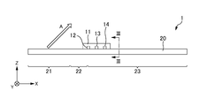
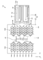
- FIG. 1 is a plan view of the wireless module according to the first embodiment.
- FIG. 2 is a side view of the wireless module of the first embodiment.
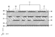
- FIG. 3 is a cross-sectional view of the plate-like array antenna of the first embodiment.
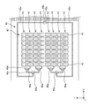
- FIG. 4 is an enlarged plan view of the main part of the plate-like array antenna of the first embodiment.
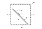
- FIG. 5 is a view showing an internal structure of a wireless device using the wireless module of the first embodiment.
- FIG. 6 is a view showing an internal structure of a wireless device using the wireless module of the first embodiment.
- FIG. 7 is an enlarged plan view of the main part of a plate-like array antenna according to a modification of the first embodiment.
- FIG. 1 is a plan view of the wireless module according to the first embodiment.
- FIG. 2 is a side view of the wireless module of the first embodiment.
- FIG. 3 is a cross-sectional view of the plate-like array antenna of the first embodiment.
- FIG. 4 is an enlarged plan view of the main
- FIG. 8 is an enlarged plan view of the main part of a plate-like array antenna according to a modification of the first embodiment.
- FIG. 9 is an enlarged plan view of the main part of a plate-like array antenna according to a modification of the first embodiment.
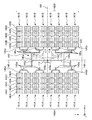
- FIG. 10 is a plan view of the wireless module of the second embodiment.
- FIG. 11 is a cross-sectional view of the plate-like array antenna of the second embodiment.
- FIG. 12 is an enlarged plan view of the main part of the plate-like array antenna of the second embodiment.
- FIG. 13 is an enlarged plan view of the main part of a plate-like array antenna according to a modification of the second embodiment.
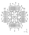
- FIG. 14 is an enlarged plan view of the main part of a plate-like array antenna according to a modification of the second embodiment.
- FIG. 15 is an enlarged plan view of the main part of a plate-like array antenna according to a modification of the second embodiment.
- a dielectric substrate, a ground conductor layer formed on one surface of the dielectric substrate, a plurality of serial radiation element arrays formed on the other surface of the dielectric substrate, and the other of the dielectric substrate A parallel feed line for feeding a high frequency power between the feed end point on the other surface of the dielectric substrate and the series of series radiation element rows, and the series radiation element
- the row has a plurality of radiation elements arranged in series at equal intervals in a straight line and connected in series, and the parallel feed line is connected to the feed end point, and the parallel feed line is selected from the plurality of radiation elements of the series type radiation element row.
- the radiation element of the end closest to the feed end point is branched into the number of rows of the series radiation element rows of the plurality of rows, and the radiation element of the nearest end and the feed end point are connected, and the plurality of series radiation element rows
- the pitches of the plurality of radiation elements are equal, and the plurality of rows
- the parallel feed line path lengths equal plate array antenna along from the feed end point to the radiating elements of the nearest end is clear.
- the phases are in phase.
- the directivity of the plate-like array antenna can be appropriately set in accordance with the arrangement of the series radiation element arrays. Further, since the parallel feed line connects the radiation element at the end closest to the feed end point and the feed end point, the path length from the feed end point to the radiation element can be minimized. Therefore, while being able to aim at reduction of the transmission loss in a parallel feed line, high gain-ization of a plate-shaped array antenna can be achieved.
- the plurality of series of series radiation element arrays are arranged in parallel, and the radiation elements at the closest end of the plurality of series radiation element arrays are arranged in a line in a direction perpendicular to the series direction of the series type radiation element arrays It is done. Thereby, the direction of the maximum radiation intensity of the plate-like array antenna can be set to be inclined from the normal direction of the dielectric substrate to the feeding end point side.
- the parallel feed line is disposed in an area between the radiation element at the closest end of the series of radiation element arrays of the plurality of lines and the feed end point. Therefore, the path length from the feeding end point to the radiation element can be minimized. Therefore, while being able to aim at reduction of the transmission loss in a parallel feed line, high gain-ization of a plate-shaped array antenna can be achieved.
- the shape of the plurality of serial radiation element rows as a whole is a line symmetrical shape with respect to a symmetry line parallel to the row direction of the serial radiation element rows through the feed end point.
- the direction of the maximum radiation intensity of the plate-like array antenna can be set so as not to be inclined around the symmetry line axis from the plane perpendicular to the dielectric substrate through the symmetry line.
- the plurality of series of series radiating element rows included in the first set when the plurality of series of series radiating element arrays are divided into two sets are arranged in parallel, and the first set of series of series radiating element rows is arranged in parallel.
- the radiation elements at the nearest end are arranged in a line in a direction perpendicular to the line direction of the series of the series of series radiation elements, and the series of series of series radiation elements included in the second set is the first series Parallel to the row direction of the series of series radiating element rows of the set, the radiation elements at the nearest end of the series of series radiating element rows of the second set of series are of the second series of series type
- the first set of serial radiation element arrays and the second set of serial radiation element arrays are arranged in a line in a direction perpendicular to the column direction of the radiation element arrays, It is lined up in the column direction.
- the direction of the maximum radiation intensity of the plate-like array antenna can be set in the normal direction of the dielectric substrate.
- the feed end point is disposed in the region between the first set of series of series radiating element arrays and the second set of series of series radiating element arrays.
- the parallel feed line is disposed in the area.
- the shape of the plurality of serial radiation element rows as a whole is a line symmetrical shape with respect to a symmetry line perpendicular to the row direction of the serial radiation element rows through the feed end point.
- the shape of the plurality of serial radiation element rows as a whole is a line symmetrical shape with respect to a symmetry line parallel to the row direction of the serial radiation element rows through the feed end point.
- the shape of the plurality of serial radiation element arrays as a whole has a two-fold rotational symmetry centered on the feed end point.
- the plurality of series of series radiating element rows included in the first set when the plurality of series of series radiating element arrays are divided into four sets are arranged in parallel, and the first set of series of series radiating element rows is arranged in parallel.
- the radiation elements of the nearest end are arranged in a direction perpendicular to the column direction of the first set of serial radiation element arrays, and the plurality of series of serial radiation element arrays included in the second set are of the first set.
- the radiation elements of the nearest end of the second series of the series of series radiation array columns are arranged in parallel so as to be parallel to the series direction of the series radiation array, and the second series of series radiation elements
- the first set of plural series of serial radiating element arrays and the second set of plural series of serial radiating element arrays are arranged in the direction perpendicular to the column direction of the columns.
- the plurality of series of series radiating element rows included in the third set are perpendicular to the column direction of the first set of series radiating element rows
- the radiation elements at the closest end of the third set of series radiation element arrays are arranged in a direction perpendicular to the column direction of the third set of series radiation element arrays.
- a plurality of series of series radiating element rows included in the fourth set are arranged in parallel to be parallel to a row direction of the third set of series radiating elements, and the fourth set of series of series
- the radiation elements at the closest end of the radiation element array are arranged in a direction perpendicular to the column direction of the fourth set of series radiation element arrays, and the third set of plural series of series radiation element arrays and The fourth set of plural series of series radiating element arrays are arranged in the column direction, and the first set of plural series of series radiating element arrays and the second set of plural series of series radiating element arrays Between the third set of series of multiple series of radiating elements and the fourth set of series of series of series radiating elements That.
- the direction of the maximum radiation intensity of the plate-like array antenna can be set in the normal direction of the dielectric substrate.
- the number of radiating elements can be increased, and the gain of the plate-like array antenna can be increased.
- the feed point is located in the area.
- the parallel feed line is disposed in the area.
- the transmission loss in the parallel feed line can be reduced, and the gain of the plate-like array antenna can be increased.
- the shape of the plurality of serial radiation element rows as a whole is a line symmetrical shape with respect to a symmetry line parallel to the row direction of the first set of serial radiation element rows through the feed end point.
- the shape of the plurality of serial radiation element rows as a whole is a line symmetrical shape with respect to a symmetry line parallel to the row direction of the third set of serial radiation element rows through the feed end point.
- the shape of the plurality of serial radiation element rows as a whole has a four-fold rotational symmetry centered on the feed end point.
- the plate-like array antenna is further connected to the parallel feeding circuit at a midpoint between the feeding end point and a radiation element at an end closest to the feeding end point, and further includes a plurality of amplifiers for amplifying signals passing through the parallel feeding circuit.
- the plurality of amplifiers are arranged in point symmetry with respect to the feed end point. Thereby, long distance transmission of radio waves can be realized by signal amplification.
- a wireless module comprising the plate-like array antenna and an electronic component mounted on the surface of the plate-like array antenna, wherein a feeding terminal of the electronic component is connected to the feeding end point is apparent. Thereby, the transmission loss between the electronic component and the parallel feed line can be suppressed.
- FIG. 1 is a plan view of the wireless module 1
- FIG. 2 is a side view of the wireless module 1
- FIG. 3 is a cross-sectional view of III-III shown in FIG. It is an enlarged plan view of the principal part of
- the X axis, the Y axis, and the Z axis are illustrated as auxiliary lines or symbols indicating directions.
- the X axis, the Y axis and the Z axis are orthogonal to one another.
- the wireless module 1 is a module for transmitting, receiving, or transmitting / receiving radio waves in a microwave or millimeter wave frequency band.
- the wireless module 1 includes a plate-like array antenna 20 and electronic components 11 to 17 mounted on the surface of the plate-like array antenna 20.
- the X-axis shown in FIGS. 1 to 3 is parallel to the long side of the rectangular plate-like array antenna 20, and the Y-axis is parallel to the short sides 24 and 25 of the plate-like array antenna 20.
- the X axis and the Y axis are parallel to the front and back surfaces of the plate-like array antenna 20, respectively.
- the plate-like array antenna 20 is a multilayer wiring board.
- the plate-like array antenna 20 includes a dielectric adhesion layer 31, dielectric base materials 32, 33, conductor pattern layers 34, 35, 36, a ground conductor layer 37, and passivation films 38, 39.
- a thin plate dielectric substrate 32 and a thin plate dielectric substrate 33 are bonded by a dielectric adhesive layer 31.
- the dielectric base 32, the dielectric adhesive layer 31, and the dielectric base 33 are stacked in this order, and the stack becomes a dielectric substrate.
- the dielectric substrates 32, 33 are made of, for example, a resin (for example, liquid crystal polymer, polyimide, polyethylene terephthalate), a fiber reinforced resin (for example, glass cloth epoxy resin), a fluorine resin or a ceramic.
- the dielectric bonding layer 31 is made of, for example, an epoxy resin.
- a conductor pattern layer 34 is formed between the dielectric base 32 and the dielectric adhesive layer 31, and a conductor pattern layer 35 is formed between the dielectric base 33 and the dielectric adhesive layer 31.
- the conductor pattern layers 34 and 35 are covered with the dielectric bonding layer 31 by bonding the dielectric base 32 and the dielectric base 33 by the dielectric bonding layer 31.
- the conductor pattern layer 34 processes (patterns) the conductor layer (for example, a metal plating layer) formed on the surface on the dielectric adhesive layer 31 side of the dielectric base 32 by photolithography and etching. It was obtained by The same applies to the conductor pattern layer 35.
- a conductor pattern layer 36 is formed on the surface of the dielectric base 32 opposite to the dielectric adhesive layer 31. Furthermore, on the surface, a passivation film 38 is formed to coat the conductor pattern layer 36.
- the conductor pattern layer 36 is obtained by processing the conductor layer formed on the dielectric base 32 by photolithography and etching. The conductor pattern layer 36 will be described in detail later.
- a ground conductor layer 37 is formed on the surface of the dielectric base 33 opposite to the dielectric adhesive layer 31. Furthermore, a passivation film 39 is formed on the surface so as to coat the ground conductor layer 37.
- the ground conductor layer 37 is obtained by processing the conductor layer formed on the dielectric base material 33 by photolithography and etching or the like.
- the ground conductor layer 37 may be a layer formed on the entire surface of the dielectric base 33 opposite to the dielectric adhesive layer 31 without being patterned.
- the passivation films 38 and 39 are made of insulating and dielectric materials.
- the dielectric base 32 and the conductor pattern layer 36 are protected by the passivation film 38, and the dielectric base 33 and the ground conductor layer 37 are protected by the passivation film 39.
- the electronic component 11 is formed on the above-described plate-like array antenna 20, that is, on the surface of the dielectric base 32 opposite to the dielectric adhesive layer 31. 17 are surface mounted.
- the electronic component 11 is a so-called RFIC (Radio Frequency Integrated Circuit), and is formed of an integrated circuit (IC) in which a receiver circuit, a transmitter circuit, or both of them are incorporated.
- the receiving circuit incorporated in the electronic component 11 is composed of, for example, a tuning circuit, a demodulation circuit, and an amplifier
- the transmitting circuit incorporated in the electronic component 11 is composed of, for example, an oscillating circuit, a modulation circuit, and an amplifier.
- the terminals of the electronic component 11 are connected to the conductor pattern layer 36 by, for example, a BGA (Ball Grid Array) method or an LGA (Land Grid Array) method using solder or the like.
- the electronic components 12 to 17 are, for example, a resistor (resistor), a capacitor (capacitor), an inductor (coil) or a vibrator.
- the terminals of the electronic components 12 to 17 are connected to the conductor pattern layer 36 using solder or the like.
- the plate-like array antenna 20 is divided into three rectangular regions 21 to 23 as shown in FIGS.
- the area 21 is a rectangular area on one short side 24 side
- the area 23 is a rectangular area on the other short side 25 side
- the area 22 is a rectangular area between the area 21 and the area 23.
- the region 21 may be referred to as an antenna formation region
- the region 22 may be referred to as a feed line formation region
- the region 23 may be referred to as a signal line formation region 23.
- the electronic components 11, 13, 14, 16 and 17 are mounted closer to the feed line formation region 22 in the signal line formation region 23.
- the electronic components 12 and 15 are mounted near the signal line formation area 23 in the feed line formation area 22.
- the electronic components 11 to 17 are disposed close to each other.
- the electronic component 11 partially protrudes from the signal line formation area 23 to the feed line formation area 22.
- the conductor pattern layer 36 By patterning the conductor pattern layer 36, the conductor pattern layer 36 includes 2 n columns (n is an integer of 1 or more) of serial radiation element columns 41 and 2 n distributed parallel feed lines 45. A pair of ground conductors 51 and a large number of wires 55 are provided. In the example shown in FIGS. 1 and 4, n is 2 and the number of series radiation element rows 41 is four, but if the antenna formation region 21 is wider than the case shown in FIGS. 1 and 4 The number of the series radiation element arrays 41 may be more. The greater the number of series radiating element rows 41, the higher the gain of the antenna. In the following description, the “series type radiation element array” is abbreviated as “element array”.
- a pair of ground conductor portions 51 are formed on both sides in the Y direction of the signal line formation region 23 at an interval therebetween, and a part 51a of the ground conductor portion 51 is from the signal line formation region 23 to the feed line formation region. It covers 22.
- the interval 51c between the portions 51a extending to the feed line forming region 22 is narrower than the interval between the remaining portions 51b.
- the electronic components 11 to 17 are disposed closer to the short side 25 of the plate-like array antenna 20 than the portion 51a of the ground conductor portion 51 which extends to the feed line forming region 22 and the remaining portions 51b. It is arranged between.
- the ground conductor portion 51 is connected to the terminals of the electronic components 11 to 17, and a reference potential (ground potential) is applied from the ground conductor portion 51 to the terminals of the electronic components 11 to 17. Further, the ground conductor portion 51 is connected to the ground conductor layer 37 (see FIG. 3) via a via hole, and a reference potential is applied from the ground conductor portion 51 to the ground conductor layer 37.
- the wires 55 are formed in the signal line formation region 23 so as to be routed in the long side direction (X direction) of the plate array antenna 20 from the short side 25 of the plate array antenna 20 toward the feed line formation region 22. It is done.
- the end 55 a of the wire 55 is formed in an island shape so as to be wider than the other portions, and is arranged along the short side 25 of the plate-like array antenna 20.
- the ends 55a of the wires 55 are connection terminals.
- the end 55a of the wiring 55 is exposed without being covered by the passivation film 38, and the end 55a of the wiring 55 is connected to the terminal of another device when the wireless module 1 is mounted on the other device.
- wires 55 are routed from the short side 25 of the plate-like array antenna 20 to the ground conductor 51 and connected to the ground conductor 51, and the rest are between the pair of ground conductors 51. Are drawn from the short side 25 of the plate-like array antenna 20 to the vicinity of the electronic components 11 to 17 and connected to the terminals of the electronic components 11 to 17. Some of the wirings 55 connected to the terminals of the electronic components 11 to 17 may be directly connected to the terminals of the electronic components 11 to 17, and the electronic components 11 to 17 may be formed via via holes and conductor pattern layers 34 and 35. Some are connected to the terminal of.
- a power supply line for supplying a power supply voltage to the electronic component 11, a clock line for supplying an operation clock to the electronic component 11, and various signals for the electronic component 11 to 17 are connected to the wiring 55 connected to the terminals of the electronic components 11 to 17. There is a signal line etc. to supply.
- the element array 41 has a plurality of patch-type radiating elements 42 and a direct feed line 43.
- the number of radiating elements 42 included in the single element row 41 is four, but the number may be two to three or five or more. The greater the number of radiating elements 42 included in the element array 41, the higher the gain of the antenna. It is desirable to increase the number of radiating elements 42 as much as possible in accordance with the size and shape of the antenna formation region 21.
- a plurality of radiating elements 42 are linearly arranged at equal intervals in the long side direction (X direction) of the plate-like array antenna 20. These radiation elements 42 are connected in series by direct feed lines 43 provided between adjacent ones.
- the element array 41 of 2 n columns as described above is juxtaposed at equal intervals in the short-side direction (Y direction) of the plate-like array antenna 20, whereby the radiating elements 42 become the entire element array 41 of 2 n columns. They are arranged in a grid.
- the radiation elements 42 at the end closest to the feed end point 45s (feed terminal of the electronic component 11) of the parallel feed line 45 among the element rows 41 are aligned in the X direction. That is, the radiation element 42 at the end closest to the feed end point 45s of the parallel feed line 45 in each element row 41 has one row in the direction (Y direction) perpendicular to the row direction (X direction) of the element row 41.
- the intervals between the adjacent element rows 41 are all equal.
- the distance between the adjacent radiation elements 42 in the Y direction and the distance between the adjacent radiation elements 42 in the X direction may be equal to or different from each other.
- radiation element array 40 what the element row
- the radiating element array 40 has a line symmetrical shape with respect to a symmetry line 49 parallel to the row direction (X direction) of the element row 41 through feed end points 45s (feed terminals of the electronic component 11) of the parallel feed line 45 described later. Is formed. Since the number of element rows 41 is an even number, none of the element rows 41 are arranged on the symmetry line 49.
- a ground conductor layer 37 (see FIG. 3) is formed so as to extend over the entire antenna formation region 21 so that the radiation element array 40 functions as a microstrip antenna, and a dielectric is formed between the ground conductor layer 37 and the radiation element 42.
- a parallel feed line 45 is formed in the feed line formation region 22.
- the parallel feed line 45 connects the element row 41 of 2 n rows and the feed terminal of the electronic component 11.
- the connection portion between the parallel feed line 45 and the feed terminal of the electronic component 11 is the feed end point 45 s of the parallel feed line 45.
- the electronic component 11 supplies high-frequency power to the parallel feed line 45 through the feed terminal and the feed end point 45s.
- the parallel feed line 45 is for distributing the high-frequency power supplied to the feeding end point 45s by the electronic component 11 to the element row 41 of 2 n rows for transmission.
- the parallel feed line 45 combines the high frequency power generated in the 2 n row of element rows 41 by the reception of radio waves, and generates electrons through the feed end point 45s and the feed terminal. It is transmitted to the part 11.
- the parallel feed line 45 has n stages of T-shaped distribution units 45a, and the distribution unit 45a extends from the feed end point 45s to the element array 41 (in particular, the radiating element 42 at the end closest to the feed end point 45s of the parallel feed line 45). It is formed in a tree shape branched to 2 n .
- the distribution unit 45a is a combining unit.
- the number of distribution units 45 a in the m- th stage (m is an arbitrary integer from 1 to n) from the feed terminal of the electronic component 11 is 2 m ⁇ 1 .
- the electronic component 11 to the first stage distribution unit 45a are connected to the feed terminal of the electronic component 11 via the feed line 45b.
- the connection portion between the feed line 45 b and the feed terminal of the electronic component 11 is the feed end point 45 s of the parallel feed line 45.
- the feed line 45b extends in the X direction at the interval 51c between the portions 51a of the ground conductor 51 which extend over the feed line formation region 22 and extends from the first stage distribution portion 45a to the feed end point 45s. It is done.
- the distribution units 45a of the adjacent stages are connected by a feed line 45c.
- the distribution part 45a from the electronic component 11 to the nth stage is connected to the element row 41 (in particular, the radiation element 42 at the end closest to the feed end point 45s of the parallel feed line 45) via the feed line 45d
- Each of the distribution units 45a distributes the high frequency power transmitted from the electronic component 11 or the distribution unit 45a of the previous stage into two, and the distribution unit 45a or the element array 41 of the latter stage (in particular, the feed end 45s of the parallel feed line 45 is most It transmits to the radiation element 42) of the near end (in the case of transmission). Further, each of the distributors 45a combines the high-frequency power transmitted from the distributor 45a in the rear stage or the element array 41 (in particular, the radiating element 42 at the end closest to the feed end point 45s of the parallel feed line 45). It transmits to the part 11 or the distribution part 45a of a front
- the parallel feed lines 45 as described above are formed in line symmetry with respect to the symmetry line 49.
- the path length (electrical length) from the radiating element 42 at the end closest to the feed end point 45s of the parallel feed line 45 to the feed end point 45s of the parallel feed line 45 through the parallel feed line 45 is equal. Therefore, the feed of the same phase is performed to any radiation element 42 of the end closest to the feed end point 45s of the parallel feed line 45.
- the radiating element array 40 is formed in a line symmetrical shape with respect to the symmetry line 49, feeding elements in the same phase are provided to the radiation elements 42 arranged at mutually symmetrical positions with respect to the symmetry line 49. Furthermore, the feeding of the same phase is performed on the radiation elements 42 arranged the same from the parallel feed line 45 side.
- the radiating element array 40 Since the element row 41 is a series feeding system, the radiating elements 42 included in the same element row 41 are delayed in phase of feeding as they are separated from the parallel feeding line 45. Therefore, the radiating element array 40 has a radio wave directivity having a maximum radiation intensity in a direction inclined toward the electronic component 11 with respect to the normal direction of the plate-like array antenna 20 (see arrow A in FIG. 2).
- the maximum radiation intensity angle of the radiating element array 40 is more than 0 ° and less than 90 ° with respect to the normal of the plate-like array antenna 20.
- ground conductor layer 37 (see FIG. 3) is formed to extend over the entire feed line formation region 22 so that the parallel feed line 45 functions as a microstrip line type signal transmission line.
- the conductor pattern layers 34 and 35 do not extend to the feed line forming region 22.
- the radiating element array 40 has a plurality of radiating elements 42 arranged in a grid in the X and Y directions. Therefore, the number of radiating elements 42 is large and the area of the radiating element array 40 is large. Therefore, high gain of the radiation element array 40 can be realized, and long distance transmission of radio waves can be realized.
- the path length from the radiation element 42 closest to the feed end point 45s of the parallel feed line 45 in the element row 41 to the feed end point 45s (feed terminal of the electronic component 11) of the parallel feed line 45 is any element line 41 But it is equal. Furthermore, the pitch in the X direction of the element row 41 is equal in any of the element rows 41. Therefore, the feeding of the same phase is performed to the radiation elements 42 arranged the same from the parallel feed line 45 side. Therefore, the direction of maximum radiation intensity is the same in any element row 41, and high gain of the radiating element array 40 can be realized. Further, the maximum radiation intensity angle of the radiation element array 40 can be inclined with respect to the normal direction of the plate-like array antenna 20.
- All the distribution parts 45 a of the parallel feed line 45 are arranged in the region between the radiation element array 40 and the electronic component 11. Therefore, the path length from the radiation element 42 to the feed end point can be minimized, and the transmission loss in the parallel feed line 45 can be suppressed.
- the parallel feed line 45 is connected to the radiation element 42 closest to the feed end point 45s of the parallel feed line 45 in the element row 41. Therefore, the path length from the radiation element 42 to the feed end point 45s of the parallel feed line 45 can be minimized, and the transmission loss in the parallel feed line 45 can be suppressed.
- the parallel feed line 45 and the radiating element array 40 are formed in a common layer. That is, the parallel feed line 45 and the radiation element array 40 are obtained by patterning the common conductor layer. Therefore, the path length from the radiation element 42 closest to the feed end point 45s of the parallel feed line 45 in the element row 41 to the feed end point 45s of the parallel feed line 45 can be minimized, and the transmission loss in the parallel feed line 45 Can be reduced.
- the parallel feed lines 45 are not provided across a plurality of layers, but are formed in one layer. That is, the parallel feed line 45 does not have a via hole or a through hole. Therefore, in the parallel feed line 45, no transmission loss occurs due to the misalignment between the layers.
- the electronic component 11 is mounted on the plate-like array antenna 20, and the feed terminal of the electronic component 11 is directly connected to the feed end point 45 s of the parallel feed line 45. Therefore, the transmission loss between the electronic component 11 and the parallel feed line 45 can be reduced.
- FIG. 5 is a view showing an internal structure of a wireless device 80 using the wireless module 1.
- the wireless device 80 includes the wireless module 1, a housing 81, a printed circuit board 82, and a connector 83.
- the housing 81 is formed in a box shape, and the wireless module 1, the printed circuit board 82 and the connector 83 are accommodated in the housing 81.
- the printed circuit board 82 is fixed in the housing 81 in a state of being inclined with respect to the bottom surface portion 81 a of the housing 81.
- a connector 83 is mounted on the printed circuit board 82.
- the wireless module 1 is mounted on the printed circuit board 82 by the connector 83.
- the end of the wiring 55 is engaged by fitting the end of the short side 25 of the plate-like array antenna 20 to the connector 83 in a state where the plate-like array antenna 20 is erected with respect to the printed circuit board 82.
- 55a is connected to the circuit of the printed circuit board 82 through the terminal of the connector 83.
- the circuit of the printed circuit board 82 is provided with a control unit, a baseband unit, a power supply circuit, an input / output interface and the like.
- the printed circuit board 82 is inclined with respect to the bottom surface 81 a of the housing 81 It is provided in the housing 81.
- the maximum radiation direction of the radiation element array 40 is directed to the front surface 81 b of the housing 81 and is substantially perpendicular to the front surface 81 b of the housing 81.
- the front surface 81b of the housing 81 is made of a dielectric material, and radio waves are not blocked by the front surface 81b.
- FIG. 6 is a view showing the internal structure of a wireless device 90 using the wireless module 1.
- the wireless device 90 includes the wireless module 1, a housing 91, a printed circuit board 92, and a connector 93.
- the wireless module 1, the printed circuit board 92, and the connector 93 are accommodated in a box-like housing 91.
- the printed circuit board 92 is fixed in the housing 91 in a state of being inclined with respect to the bottom surface portion 91 a of the housing 91.
- a connector 93 is mounted on the printed circuit board 92.
- the wireless module 1 is mounted on the printed circuit board 92 by the connector 93.
- the end portion of the wiring 55 is fitted by fitting the end portion on the short side 25 side of the plate-like array antenna 20 to the connector 93 with the plate-like array antenna 20 lying down against the printed circuit board 92.
- 55a is connected to the circuit of the printed circuit board 92 through the terminal of the connector 93.
- the circuit of the printed circuit board 92 is provided with a control unit, a baseband unit, a power supply circuit, an input / output interface and the like.
- the printed circuit board 92 is provided in the housing 91 in a state of being inclined with respect to the bottom surface portion 91 a of the housing 91.
- the maximum radiation direction of the radiation element array 40 is directed to the front surface 91 b of the housing 91 and is substantially perpendicular to the front surface 91 b of the housing 91.
- the front surface portion 91b of the housing 91 is made of a dielectric material, and radio waves are not blocked by the front surface portion 91b.
- n is two, the number of element rows 41 is four, and the parallel feed line 45 is a four-distribution tree-like feed line having the two-stage distribution unit 45 a.
- n is three, the number of element rows 41 is eight, and the parallel feed line 45 is an eight-distributed tree-like feed line having three stages of distribution units 45a. It may be.
- the number of radiating elements 42 included in one element row 41 is eight.
- the shape of the radiation element 42 shown in FIG. 7 and the shape of the radiation element 42 shown in FIG. 4 are congruent.
- the radiation element array 40 shown in FIG. 7 has a larger number of radiation elements 42 and a wider area than the radiation element array 40 shown in FIG. 4. Therefore, the radiating element array 40 shown in FIG. 7 has a higher gain than the radiating element array 40 shown in FIG.
- the number of radiating elements 42 is equal in all element rows 41.
- these element rows 41 may have different numbers of radiating elements 42 because of the shape of the antenna formation region 21 and the like.
- the number of radiating elements 42 in the central two rows of element rows 41 is six, and the number of radiating elements 42 in the two rows of element rows 41 on both sides is four,
- the number 42 gradually decreases from the middle row to the side rows.
- the number of radiating elements 42 in the row gradually decreases in units of two from the center row to the side row due to the shape of the antenna forming region 21, but the antenna forming region If the shape of 21 is different, it may be gradually reduced by one. In order to increase the gain of the antenna, it is desirable to have as many radiating elements 42 as possible. Also, although not shown, the number of radiating elements 42 in the row may be gradually increased from the center row to the side rows.
- the parallel feed line 45 shown in FIGS. 4 and 7 feeds the radiation element 42 closest to the feed end point 45s of the parallel feed line 45 in the element row 41.
- the parallel feed line 45 shown in FIG. 9 feeds the radiation element 42 farthest from the feed end point 45s of the parallel feed line 45 in the element row 41.
- the distribution part 45a of the first stage of the parallel feed line 45 shown in FIG. 9 is disposed in the region between the radiation element array 40 and the electronic component 11, and the distribution parts 45a of the second and subsequent stages are radiation elements.
- the feed line 45c which is disposed in the area opposite to the electronic component 11 with respect to the array 40, and is connected to the first stage distribution unit 45a and the second stage distribution unit 45a It is routed to the opposite side of the electronic component 11 from the side.
- the maximum radiation intensity angle of the radiation element array 40 is inclined to the opposite side of the electronic components 11 to 17 with respect to the normal direction of the plate-like array antenna 20.
- FIG. 10 is a plan view of the wireless module 101
- FIG. 11 is a cross-sectional view of a plate-like array antenna 120 of the wireless module 101
- FIG. 12 is an enlarged plan view of the main part of the wireless module 101.
- an X axis, a Y axis, and a Z axis are illustrated as auxiliary lines indicating directions.
- the X axis, the Y axis and the Z axis are orthogonal to one another.
- the wireless module 101 is a module for transmitting, receiving, or transmitting / receiving radio waves in a microwave or millimeter wave frequency band.
- the wireless module 101 includes a plate-like array antenna 120 and electronic components 111 to 117 mounted on the surface of the plate-like array antenna 120.
- the X-axis and the Y-axis are parallel to the front surface and the back surface of the plate-like array antenna 120.
- the plate-like array antenna 120 is formed in such a shape that the short sides of the rectangular plate-like portion 126 are connected continuously to the central portion of one side of the rectangular plate-like portion 127 .
- the plate-like array antenna 120 is similar to the plate-like array antenna 20 of the first embodiment in that the dielectric bonding layer 131, the dielectric bases 132 and 133, and the conductor pattern layers 134 and 135. 136, a ground conductor layer 137, and passivation films 138 and 139.
- the dielectric adhesion layer 131, the dielectric bases 132 and 133, the conductor pattern layers 134, 135 and 136, the ground conductor layer 137, and the passivation films 138 and 139 in the second embodiment are the dielectric adhesion in the first embodiment, respectively. It corresponds to the layer 31, the dielectric bases 32 and 33, the conductor pattern layers 34, 35 and 36, the ground conductor layer 37, and the passivation films 38 and 39.
- the plate-like array antenna 120 is divided into three rectangular regions 121 to 123.
- a region 121 is a rectangular frame-like region around the rectangular plate-like portion 127
- a region 122 is a rectangular region at the center of the rectangular plate-like portion 127 surrounded by the region 121
- a region 123 is a rectangular plate-like portion It is a rectangular area corresponding to 126.
- the region 121 may be referred to as an antenna formation region 121
- the region 122 may be referred to as a feed line formation region 122
- the region 123 may be referred to as a signal line formation region 123.
- Electronic Components As shown in FIGS. 10 and 12, electronic components 111 to 117 are formed on the plate-like array antenna 120, that is, on the surface of the dielectric base 132 opposite to the dielectric adhesive layer 131. Has been implemented. The mounting positions of the electronic components 111 to 117 are at the center of the feed line formation region 122. The electronic components 111 to 117 of the second embodiment correspond to the electronic components 11 to 17 of the first embodiment.
- the conductor pattern layer 136 By patterning the conductor pattern layer 136, the conductor pattern layer 136 includes 2 n columns (n is an integer of 1 or more) of element rows 141A and 141B, and 2 n distributed parallel feed lines 145, A ground conductor portion 151 and a large number of wires 155 are provided.
- n is 4, the total number of element rows 141A and 141B is 16, the number of element rows 141A is 8, and the number of element rows 141B is It is eight.
- the ground conductor portion 151 is formed in a U shape (U-shape) along the long sides on both sides of the signal line formation region 123 and the short side of the rectangular plate portion 126 on the rectangular plate portion 127 side. .
- the ground conductor portion 151 is connected to the terminals of the electronic components 111 to 117 through the via holes and the conductor pattern layers 134 and 135, and the ground potential of the ground conductor portion 151 to the terminals of the electronic components 111 to 117 is Applied. Further, the ground conductor portion 151 is connected to the ground conductor layer 137 (see FIG. 11) via a via hole, and a reference potential is applied from the ground conductor portion 151 to the ground conductor layer 137.
- the wiring 155 is routed so as to be routed in the long side direction (X direction) of the rectangular plate-like portion 126 from the short side 125 of the rectangular plate-like portion 126 of the plate-like array antenna 120 toward the rectangular plate-like portion 127. It is formed in the line formation area 123.
- the end portion 155 a of the wire 155 is formed in an island shape so as to be wider than the other portions, and is arranged along the short side 25 of the rectangular plate-like portion 126.
- the ends 155a of the wires 155 are connection terminals.
- the end 155 a of the wiring 155 is exposed without being covered by the passivation film 138.
- the wires 155 are routed from the short side 125 of the rectangular plate-like portion 126 of the plate-like array antenna 120 to the ground conductor portion 151 and connected to the ground conductor portion 151.
- the remaining wires 155 are drawn from the short side 125 of the rectangular plate-like portion 126 of the plate-like array antenna 120 toward the opposite short side, and the electronic component 111 is formed via the via holes and conductor pattern layers 134 and 135.
- the wiring 155 connected to the terminals of the electronic components 111 to 117 includes a power supply line that supplies a power supply voltage to the electronic component 111, a clock line that supplies an operation clock to the electronic component 111, and various signals to the electronic components 111 to 117. There is a signal line etc. to supply.
- 2 n element rows are formed in the antenna formation area 121. Specifically, 2 n-1 row of element array 141A and the 2 n-1 column element array 141B is arranged on the antenna forming region 121 at the feed line forming region 122 between them.
- the element row 141 ⁇ / b> B is disposed closer to the rectangular plate portion 126 than the feed line formation region 122.
- the element row 141A is disposed on the opposite side of the element row 141B with respect to the feed line formation region 122.
- the element row 141A includes a plurality of patch radiation elements 142A and a direct feed line 143A.
- a plurality of radiation elements 142A are linearly arranged at equal intervals in the long side direction (X direction) of the rectangular plate-like portion 126 of the plate-like array antenna 120.
- the pitch (the pitch is the distance between the adjacent radiation elements 142A in the X direction) of each of the element rows 141A is equal to each other.
- These radiation elements 142A are connected in series by the direct feed line 143A provided between the adjacent ones.
- the number of radiating elements 142A included in the element row 141A in one row is four, but the number may be two to three or five or more.
- the number of radiating elements 142A is the same in all of the element rows 141A. However, the number of radiating elements 142 may be different in these element rows 141A.
- the element array 141A of 2 n -1 lines as described above are arranged at equal intervals in the short side direction (Y direction) of the rectangular plate-like portion 126 of the plate-like array antenna 120, whereby 2 n -1 elements of elements As a whole of the row 141A, the radiating elements 142A are arranged in a grid.
- the radiation element 142A of the end closest to the feed end point 145s (feed terminal of the electronic component 111) of the parallel feed line 145 in each element row 141A is aligned in the X direction.
- the radiation element 142A at the end closest to the feed end point 145s (feed terminal of the electronic component 111) of the parallel feed line 145 in each element row 141A is perpendicular to the column direction (X direction) of the element row 141A. It is arranged in a line in one direction (Y direction).
- the intervals between the adjacent element rows 141A are all equal.
- the spacing between the radiating elements 142A adjacent in the Y direction and the spacing between the radiating elements 142A adjacent in the X direction may be equal to or different from each other.
- the element array 141A in parallel is referred to as a radiation element array 140A.
- Radiating element array 140A has a symmetrical shape with respect to a symmetry line 149 parallel to the row direction (X direction) of element row 141A through feed end point 145s (feed terminal of electronic component 111) of parallel feed line 145 described later. Is formed. Since the number of element rows 141A is even, none of the element rows 141A are arranged on the symmetry line 149. Even when the number of radiating elements 142 of the plurality of element rows 141A included in the radiating element array 140A is not equal, the radiating element array 140A is formed in a line symmetrical shape with respect to the symmetry line 149.
- the element row 141B includes a plurality of patch-type radiating elements 142B linearly arranged at equal intervals in the long side direction (X direction) of the rectangular plate-like portion 126 of the plate-like array antenna 120; And a direct feed line 143B connecting the radiation elements 142B in series.
- the pitches are equal to each other in any element row 141B.
- the arrangement direction of the radiation elements 142B of the element row 141B and the arrangement direction of the radiation elements 142A of the element row 141A are parallel to each other.
- the pitch of the radiating elements 142B of the element row 141B (the spacing between the radiating elements 142B adjacent to each other in the X direction) and the pitch of the radiating elements 142A of the element row 141A (the spacing between the neighboring radiating elements 142A in the X direction) are equal to each other.
- the number of radiating elements 142B included in one element row 141B is equal to the number of radiating elements 142A included in one element row 141A.
- the element array 141 B of 2 n -1 lines as described above are arranged at equal intervals in the short side direction (Y direction) of the rectangular plate-like portion 126 of the plate-like array antenna 120, whereby 2 n -1 elements of elements As a whole of the column 141B, the radiating elements 142B are arranged in a grid.
- the radiation element 142B of the end closest to the feed end point 145s (feed terminal of the electronic component 111) of the parallel feed line 145 among the element rows 141B is aligned in the X direction.
- the radiation element 142B at the end closest to the feed end point 145s of the parallel feed line 145 in each element row 141B is a single row in the direction (Y direction) perpendicular to the row direction (X direction) of the element row 141B.
- the spacing between the adjacent element rows 141B (the spacing between the adjacent radiating elements 142B in the Y direction) is equal to the spacing between the adjacent element rows 141A (the spacing between the adjacent radiating elements 142A in the Y direction).
- radiation element array 140B what the element row 141B was paralleled is called radiation element array 140B.
- the radiating element array 140B and the radiating element array 140A are aligned in the column direction (X direction) of the element rows 141A and 141B, and there is a feed line forming region 122 between the radiating element array 140B and the radiating element array 140A.
- the composite shape of the radiating element array 140A and the radiating element array 140B is axisymmetrical with respect to a symmetry line 148 orthogonal to the symmetry line 149 at the feed end point 145s of the parallel feed line 145.
- the composite shape of the radiating element array 140A and the radiating element array 140B has a two-fold rotational symmetry centered on the feed end point 145s of the parallel feed line 145.
- the ground conductor layer 137 (see FIG. 3) is formed to extend over the entire antenna formation region 121, and the ground conductor layer 137 and the radiating elements 142A and 142B are formed.
- a parallel feed line 145 is formed in the feed line formation region 122.
- the parallel feed line 145 is connected between the element arrays 141 A and 141 B in 2 n -1 rows and the feed terminal of the electronic component 111.
- the connection portion between the parallel feed line 145 and the feed terminal of the electronic component 111 is the feed end point 145 s of the parallel feed line 145.
- the electronic component 111 supplies high-frequency power to the parallel feed line 145 through the feed terminal and the feed end point 145s.
- the parallel feed line 145 distributes and transmits the high-frequency power supplied from the electronic component 111 to the feed end point 145s to the element arrays 141A and 141B of 2 n -1 rows.
- the parallel feed line 145 has n stages of T-shaped distribution parts 145a, and is formed in a tree shape branched to 2 n from the power supply terminals of the electronic component 111 to the element rows 141A and 141B by the distribution parts 145a.
- the distribution unit 145a is a combining unit.
- the number of distribution units 145 a in the m- th stage (m is an arbitrary integer from 1 to n) from the feed terminal of the electronic component 111 is 2 m ⁇ 1 .
- the feed end point 145 s of the parallel feed line 145 is the first stage distribution unit 145 a from the electronic component 111, and the feed terminal of the electronic part 111 is connected to the feed end point 145 s of the parallel feed line 145.
- the distribution units 145a of the adjacent stages are connected by a feed line 145c.
- the element row 141A (especially, the radiating element 142A at the end closest to the feed end point 145s of the parallel feed line 145) or the element row 141B (especially, parallel) via the feed line 145d. It is connected to the radiation element 142B of the end closest to the feed end point 145s of the feed line 145).
- Each of the distributors 145a distributes the high-frequency power transmitted from the electronic component 111 or the distributor 145a in the previous stage into two, and the distributor 145a in the latter stage, the element row 141A (especially, the feed end point 145s of the parallel feed line 145 It transmits to the radiation element 142A of the near end or the element row 141B (in particular, the radiation element 142B of the end closest to the feed end point 145s of the parallel feed line 145) (in the case of transmission).
- the distribution unit 145a at the subsequent stage the element row 141A (in particular, the radiating element 142A at the end closest to the feed end point 145s of the parallel feed line 145) or The high frequency power transmitted from the radiation element 142B at the end closest to the feed end point 145s is combined and transmitted to the electronic component 111 or the distribution unit 145a at the previous stage (in the case of reception).
- each element row 141A, 141B the path length from the radiation element 142A, 142B at the end closest to the feed end point 145s of the parallel feed line 145 to the feed end point 145s of the parallel feed line 145 through the parallel feed line 145 Electric length is equal. Therefore, the feed of the same phase is performed to any radiating element 142A, 142B of the end closest to the feed end point 145s of the parallel feed line 145.
- the radiating element array 140A is formed in a line symmetrical shape with respect to the symmetry line 149, feeding of the same phase is performed to the radiation elements 142A disposed at symmetrical positions with respect to the symmetry line 149. The same applies to the radiating element array 140B.
- the radiating elements 142A included in the same element row 141A are delayed in phase of feeding as they are separated from the parallel feed line 145. Therefore, the radiating element array 140A has radio wave directivity with the maximum radiation intensity in the direction inclined toward the electronic component 111 with respect to the normal direction of the plate-like array antenna 120. The same applies to the radiating element array 140B. Further, since the radiating element array 140A and the radiating element array 140B are axisymmetrical with respect to the symmetry line 148, the radiation intensities of the radiating element array 140A and the radiating element array 140B are approximately equal, and the inclination angles to the electronic component 111 are approximately equal. .
- the composite antenna of the radiating element array 140A and the radiating element array 140B emits maximum radiation in the direction normal to the plate array antenna 120. It has radio wave directivity that becomes strong.
- ground conductor layer 137 (see FIG. 11) is formed to extend over the entire feed line formation region 122 so that the parallel feed line 145 functions as a microstrip line type signal transmission line.
- the radiating element arrays 140A and 140B have a plurality of radiating elements 142A and 142B arranged in a grid, the number of radiating elements 142A and 142B is large, and the area of the radiating element arrays 140A and 140B is large. . Therefore, high gain of the composite antenna of the radiating element arrays 140A and 140B can be realized, and long distance transmission of radio waves can be realized.
- All the distribution parts 145a of the parallel feed line 145 are arranged in the region between the radiation element array 140A and the radiation element array 140B. Therefore, the path length from radiation element 142A, 142B to feed end point 145s can be minimized, and the transmission loss in parallel feed line 145 can be suppressed.
- the parallel feed line 145 is connected to the radiation elements 142A and 142B closest to the feed end point 145s of the parallel feed line 145 among the element rows 141A and 141B. Therefore, the path length from the radiation elements 142A and 142B to the feed end point 145s of the parallel feed line 145 can be minimized, and the transmission loss in the parallel feed line 145 can be suppressed.
- a plurality of amplifiers 150 are surface-mounted on the plate-like array antenna 120, that is, on the surface of the dielectric base 132 opposite to the dielectric adhesive layer 131.
- the amplifier 150 is provided with an amplifier 150 in the middle of a feed line 145c connecting the first stage distribution section 145a and the second stage distribution section 145a, and the signal passing through the feed line 145c is amplified by the amplifier 150. Be done.
- the feed line 145 c is divided into a portion closer to the first stage distribution unit 145 a than the amplifier 150 and a portion closer to the second stage distribution unit 145 a than the amplifier 150. And both of the divided parts are connected via the amplifier 150.
- the amplifiers 150 are arranged in point symmetry with respect to the feed end point 145 s of the parallel feed line 145. Also, these amplifiers 150 are arranged in line symmetry with respect to the symmetry line 149. In each of the amplifiers 150, the path lengths (electrical lengths) from the amplifier 150 to the feed end point 145s of the parallel feed line 145 are equal to each other.
- the amplifier 150 is connected to the wiring 155 through the via hole and conductor pattern layers 134 and 135 and the like, and the power supply voltage is supplied to the amplifier 150 from the wiring 155.
- the amplifier 150 is, for example, a preamplifier (when the electronic component 111 is a transmission circuit) or a low noise amplifier (when the electronic component 111 is a reception circuit).
- the radiation element array 140A and the radiation element array 140B are arranged in the X direction, and the feed line forming region 122 is disposed between the radiation element array 140A and the radiation element array 140B.
- the radiating element array 140C and the radiating element array 140D are aligned in the Y direction, and the feed line forming region is between the radiating element array 140C and the radiating element array 140D.
- 122 may be arranged.
- the radiating element array 140C is composed of a plurality of element rows 141C
- the radiating element array 140D is composed of a plurality of element rows 141D.
- the total number of element rows 141A, 141B, 141C, 141D is 2 n (where n is an integer of 2 or more), the number of element rows 141A is 2 n ⁇ 2 , and the number of element rows 141B is The number of columns is 2 n ⁇ 2 , the number of columns of the element column 141 C is 2 n ⁇ 2 , and the number of columns of the element column 141 D is 2 n ⁇ 2 .
- n is five, and the element rows 141A, 141B, 141C, 141D are all eight, and the total number of element rows 141A, 141B, 141C, 141D is 32.
- the element row 141C has a plurality of patch radiation elements 142C and a direct feed line 143C.
- a plurality of radiating elements 142 C are linearly arranged at equal intervals in the short side direction (Y direction) of the rectangular plate-like portion 126 of the plate-like array antenna 120.
- These radiation elements 142C are connected in series by the direct feed line 143C provided between the adjacent ones.
- the pitch (the pitch is the distance between the adjacent radiation elements 142C in the Y direction) of each of the element rows 141C is equal to each other.
- the element row 141D also includes a plurality of patch-type radiating elements 142D linearly arranged at equal intervals in the short side direction (Y direction) of the rectangular plate-like portion 126 of the plate-like array antenna 120; And a direct feed line 143D connecting the radiation elements 142D in series.
- the pitch (the pitch is the distance between the adjacent radiating elements 142D in the Y direction) of each of the element rows 141D is equal to one another.
- Element rows 141C of 2 n -2 rows are arranged at equal intervals in the long side direction (X direction) of the rectangular plate-like portion 126 of the plate-like array antenna 120, and 2 n -2 rows of element rows 141D are plate-like array antennas
- the rectangular plate-like portions 120 are arranged in parallel at equal intervals in the long side direction (X direction).
- the radiation element 142C at the end closest to the feed end point 145s (feed terminal of the electronic component 111) of the parallel feed line 145 among the element rows 141C is aligned in the Y direction. That is, the radiation element 142C at the end closest to the feed end point 145s (feed terminal of the electronic component 111) of the parallel feed line 145 in each element row 141C is perpendicular to the column direction (Y direction) of the element row 141C. It is arranged in a line in the normal direction (X direction). The same applies to the radiating element array 140D.
- the arrangement direction of the radiation elements 142C of the element row 141C and the arrangement direction of the radiation elements 142D of the element row 141D are parallel to each other.
- the arrangement direction of the radiation elements 142C and 142D of the element rows 141C and 141D is perpendicular to the arrangement direction of the radiation elements 142A and 142B of the element rows 141A and 141B.
- the pitches of all the element rows 141A, 141B, 141C, 141D are equal to one another. Further, the parallel spacing of the element row 141A, the parallel spacing of the element row 141B, the parallel spacing of the element row 141C, and the parallel spacing of the element row 141D are all equal.
- the composite shape of the radiating element arrays 140A, 140B, 140C, and 140D is axisymmetrical with respect to the symmetry lines 148 and 149.
- the composite shape of the radiating element arrays 140A, 140B, 140C, and 140D has four-fold rotational symmetry about the feed end point 145s of the parallel feed line 145.
- the parallel feed line 145 is formed in a tree shape branched into 2 n from the feed terminal of the electronic component 111 to the element rows 141A, 141B, 141C, and 141D by the distribution unit 145a of n stages. Therefore, the electronic component 111 to the n-th stage distribution unit 145a include the element row 141A (in particular, the radiating element 142A at the end closest to the feed end point 145s of the parallel feed line 145) via the feed line 145d, and the element row 141B (especially , A radiation element 142B at the end closest to the feed end point 145s of the parallel feed line 145, an element row 141C (in particular, a radiation element 142C at the end closest to the feed end point of the parallel feed line 145) or an element row 141D (especially, parallel feed) It is connected to the radiation element 142D of the end closest to the feed end point 145s of the line 145).
- the element row 141A in particular, the radiating element 142
- the composite antennas of the radiating element arrays 140A to 140D have radio wave directivity having the maximum radiation intensity in the direction of the normal to the plate-like array antenna 120 by combining the radio wave directivity of the radiating element arrays 140A to 140D.
- the composite antenna of the radiating element arrays 140A to 140D shown in FIG. 14 has a higher gain than the composite antenna of the radiating element arrays 140A and 140B shown in FIG.
- a plurality of amplifiers 150 may be surface mounted on the plate-like array antenna 120 as in the case of the above-described modified example (1) (see FIG. 15).
- the amplifier 150 is provided at an intermediate portion of the feed line 145c connecting the third stage distribution section 145a and the fourth stage distribution section 145a (see FIG. 15), and a signal passing through the feed line 145c Are amplified by the amplifier 150.
- the amplifiers 150 are arranged in point symmetry with respect to the feed end point 145 s of the parallel feed line 145. Also, these amplifiers 150 are arranged in line symmetry with respect to the symmetry line 149. In addition, these amplifiers 150 are arranged in line symmetry with respect to the symmetry line 148. In each of the amplifiers 150, the path lengths (electrical lengths) from the amplifier 150 to the feed end point 145s of the parallel feed line 145 are equal to each other.
Landscapes
- Variable-Direction Aerials And Aerial Arrays (AREA)
- Waveguide Aerials (AREA)
- Details Of Aerials (AREA)
Abstract
アンテナの高利得化を実現するとともに、アンテナの指向性を適切に設定できるようする。 板状アレイアンテナ20は、誘電体基板と、誘電体基板の一方の面に形成された地導体層37と、誘電体基板の他方の面に形成された複数列の直列型放射素子列41と、誘電体基板の他方の面に形成され、誘電体基板の他方の面上の給電端点45sと直列型放射素子列41との間で高周波電力を給電する並列給電線路と、を備える。並列給電線路45は、給電端点45sから、給電端点45sに最も近い端の放射素子42にかけて分岐して、その放射素子42と給電端点45sを接続し、直列型放射素子列41の何れも、給電端点45sから端の放射素子42までの経路長が等しい。
Description
本発明は、マイクロ波又はミリ波等といった高周波の周波数帯で使用される板状アレイアンテナ及び無線モジュールに関する。
特許文献1~3には、マイクロストリップアレイアンテナが開示されている。特に、特許文献1,3には、直列給電方式のマイクロストリップアレイアンテナと、並列給電方式のマイクロストリップアレイアンテナの両方が開示されている。
特許文献4には、導波管によって給電するスロットアレイアンテナが開示されている。導波管は、導体配線によって信号波を伝送するものではない。よって、信号波を増幅する電気回路(アンプ)を導波管の中途部に設けることができない。
特許文献4には、導波管によって給電するスロットアレイアンテナが開示されている。導波管は、導体配線によって信号波を伝送するものではない。よって、信号波を増幅する電気回路(アンプ)を導波管の中途部に設けることができない。
ところで、特許文献1~3に記載されたマイクロストリップアレイアンテナの場合、放射素子の数を多くすることによって高利得化を図ったとしても、マイクロストリップライン給電線路の経路長が長くなってしまい、給電線路における伝送損失が高くなる。結局のところ、アンテナの高利得化を図ることができない。
特に、特許文献1に記載の並列給電方式のマイクロストリップアレイアンテナの場合(特許文献1の図16参照)、放射素子の数を増やすと、給電線路が非常に長くなってしまい、給電線路の伝送損失を無視することができない。一方、特許文献3に記載の並列給電方式マイクロストリップアレイアンテナの場合(特許文献3の図7参照)、給電線路が邪魔になって多くの放射素子を配置することができない上、仮に多くの放射素子を配置することができたものとしても、給電線路の伝送損失が高くなる。
また、マイクロストリップアレイアンテナの場合、放射素子の位置や給電方式に応じてアンテナの指向性が決まるので、電波を長距離に送受信するためには、アンテナの向きを適切に設置する必要がある。そのためには、アンテナの指向性を適切に設定する必要がある。
特に、特許文献1に記載の並列給電方式のマイクロストリップアレイアンテナの場合(特許文献1の図16参照)、放射素子の数を増やすと、給電線路が非常に長くなってしまい、給電線路の伝送損失を無視することができない。一方、特許文献3に記載の並列給電方式マイクロストリップアレイアンテナの場合(特許文献3の図7参照)、給電線路が邪魔になって多くの放射素子を配置することができない上、仮に多くの放射素子を配置することができたものとしても、給電線路の伝送損失が高くなる。
また、マイクロストリップアレイアンテナの場合、放射素子の位置や給電方式に応じてアンテナの指向性が決まるので、電波を長距離に送受信するためには、アンテナの向きを適切に設置する必要がある。そのためには、アンテナの指向性を適切に設定する必要がある。
そこで、本発明は上記事情に鑑みてなされたものである。本発明の目的は、アンテナの高利得化を実現することと、アンテナの指向性を適切に設定できるようすることにある。
上記目的を達成するための主たる発明は、誘電体基板と、前記誘電体基板の一方の面に形成された地導体層と、前記誘電体基板の他方の面に形成された複数列の直列型放射素子列と、前記誘電体基板の他方の面に形成され、前記誘電体基板の他方の面上の給電端点と前記複数列の直列型放射素子列との間で高周波電力を給電する並列給電線路と、を備え、前記直列型放射素子列は、等間隔に直線状に配列されて直列接続された複数の放射素子を有し、前記並列給電線路は、前記給電端点から、前記直列型放射素子列の前記複数の放射素子のうち前記給電端点に最も近い端の放射素子にかけて前記複数列の直列型放射素子列の列数に分岐して、前記最も近い端の放射素子と前記給電端点を接続し、前記複数の直列型放射素子列は何れも前記複数の放射素子のピッチが等しく、前記複数列の直列型放射素子列の何れも、前記給電端点から前記最も近い端の放射素子までの前記並列給電線路に沿った経路長が等しい板状アレイアンテナである。
本発明の他の特徴については、後述する明細書及び図面の記載により明らかにする。
本発明によれば、板状アレイアンテナの高利得化を図ることができる。また、板状アレイアンテナの指向性を適切に設定することができる。
後述する明細書及び図面の記載から、少なくとも以下の事項が明らかとなる。
誘電体基板と、前記誘電体基板の一方の面に形成された地導体層と、前記誘電体基板の他方の面に形成された複数列の直列型放射素子列と、前記誘電体基板の他方の面に形成され、前記誘電体基板の他方の面上の給電端点と前記複数列の直列型放射素子列との間で高周波電力を給電する並列給電線路と、を備え、前記直列型放射素子列は、等間隔に直線状に配列されて直列接続された複数の放射素子を有し、前記並列給電線路は、前記給電端点から、前記直列型放射素子列の前記複数の放射素子のうち前記給電端点に最も近い端の放射素子にかけて前記複数列の直列型放射素子列の列数に分岐して、前記最も近い端の放射素子と前記給電端点を接続し、前記複数の直列型放射素子列は何れも前記複数の放射素子のピッチが等しく、前記複数列の直列型放射素子列の何れも、前記給電端点から前記最も近い端の放射素子までの前記並列給電線路に沿った経路長が等しい板状アレイアンテナが明らかとなる。
このような板状アレイアンテナにおいては、複数列の直列型放射素子列の何れも、給電端点からそれに最も近い端の放射素子までの経路長が等しいので、何れの直列型放射素子列においても給電位相が同相となる。従って、これら直列型放射素子列の配置に応じて板状アレイアンテナの指向性を適切に設定することができる。
また、並列給電線路は給電端点に最も近い端の放射素子と給電端点を接続するので、給電端点から放射素子までの経路長を最小限に抑えることができる。よって、並列給電線路における伝送損失の低減を図ることができるとともに、板状アレイアンテナの高利得化を図ることができる。
このような板状アレイアンテナにおいては、複数列の直列型放射素子列の何れも、給電端点からそれに最も近い端の放射素子までの経路長が等しいので、何れの直列型放射素子列においても給電位相が同相となる。従って、これら直列型放射素子列の配置に応じて板状アレイアンテナの指向性を適切に設定することができる。
また、並列給電線路は給電端点に最も近い端の放射素子と給電端点を接続するので、給電端点から放射素子までの経路長を最小限に抑えることができる。よって、並列給電線路における伝送損失の低減を図ることができるとともに、板状アレイアンテナの高利得化を図ることができる。
前記複数列の直列型放射素子列が並列され、前記複数列の直列型放射素子列の前記最も近い端の放射素子が前記直列型放射素子列の列方向に対して垂直な方向に一列に配列されている。
これにより、板状アレイアンテナの最大放射強度の方角を誘電体基板の法線方向から給電端点側に傾けるように設定することができる。
これにより、板状アレイアンテナの最大放射強度の方角を誘電体基板の法線方向から給電端点側に傾けるように設定することができる。
前記並列給電線路は、前記複数列の直列型放射素子列の前記最も近い端の放射素子と前記給電端点との間の領域内に配置されている。
これにより、給電端点から放射素子までの経路長を最小限に抑えることができる。よって、並列給電線路における伝送損失の低減を図ることができるとともに、板状アレイアンテナの高利得化を図ることができる。
これにより、給電端点から放射素子までの経路長を最小限に抑えることができる。よって、並列給電線路における伝送損失の低減を図ることができるとともに、板状アレイアンテナの高利得化を図ることができる。
前記複数列の直列型放射素子列全体としての形状は、前記給電端点を通って前記直列型放射素子列の列方向に対して平行な対称線に関して線対称な形状である。
これにより、板状アレイアンテナの最大放射強度の方角を、対称線を通って誘電体基板に垂直な面から対称線軸回りに傾かないように設定することができる。
これにより、板状アレイアンテナの最大放射強度の方角を、対称線を通って誘電体基板に垂直な面から対称線軸回りに傾かないように設定することができる。
前記複数列の直列型放射素子列を2組に分けた場合の第1組に含まれる複数列の直列型放射素子列が並列され、前記第1組の複数列の直列型放射素子列の前記最も近い端の放射素子が前記第1組の直列型放射素子列の列方向に対して垂直な方向に一列に配列され、第2組に含まれる複数列の直列型放射素子列が前記第1組の直列型放射素子列の列方向に対して平行となるように並列され、前記第2組の複数列の直列型放射素子列の前記最も近い端の放射素子が前記第2組の直列型放射素子列の列方向に対して垂直な方向に一列に配列され、前記第1組の複数列の直列型放射素子列と前記第2組の複数列の直列型放射素子列とは、それらの列方向に並んでいる。
これにより、板状アレイアンテナの最大放射強度の方角を誘電体基板の法線方向に設定することができる。
これにより、板状アレイアンテナの最大放射強度の方角を誘電体基板の法線方向に設定することができる。
前記給電端点が、前記第1組の複数列の直列型放射素子列と前記第2組の複数列の直列型放射素子列との間の領域内に配置されている。
前記並列給電線路が前記領域内に配置されている。
これにより、並列給電線路における伝送損失の低減を図ることができるとともに、板状アレイアンテナの高利得化を図ることができる。
前記並列給電線路が前記領域内に配置されている。
これにより、並列給電線路における伝送損失の低減を図ることができるとともに、板状アレイアンテナの高利得化を図ることができる。
前記複数列の直列型放射素子列全体としての形状は、前記給電端点を通って前記直列型放射素子列の列方向に対して垂直な対称線に関して線対称な形状である。
前記複数列の直列型放射素子列全体としての形状は、前記給電端点を通って前記直列型放射素子列の列方向に対して平行な対称線に関して線対称な形状である。
前記複数列の直列型放射素子列全体としての形状は、前記給電端点を中心とした2回対称の回転対称性を有する。
これにより、板状アレイアンテナの最大放射強度の方角を誘電体基板の法線方向に設定することができる。
前記複数列の直列型放射素子列全体としての形状は、前記給電端点を通って前記直列型放射素子列の列方向に対して平行な対称線に関して線対称な形状である。
前記複数列の直列型放射素子列全体としての形状は、前記給電端点を中心とした2回対称の回転対称性を有する。
これにより、板状アレイアンテナの最大放射強度の方角を誘電体基板の法線方向に設定することができる。
前記複数列の直列型放射素子列を4組に分けた場合の第1組に含まれる複数列の直列型放射素子列が並列され、前記第1組の複数列の直列型放射素子列の前記最も近い端の放射素子が前記第1組の直列型放射素子列の列方向に対して垂直な方向に配列され、第2組に含まれる複数列の直列型放射素子列が前記第1組の直列型放射素子列の列方向に対して平行となるように並列され、前記第2組の複数列の直列型放射素子列の前記最も近い端の放射素子が前記第2組の直列型放射素子列の列方向に対して垂直な方向に配列され、前記第1組の複数列の直列型放射素子列と前記第2組の複数列の直列型放射素子列とは、それらの列方向に並び、第3組に含まれる複数列の直列型放射素子列が前記第1組の直列型放射素子列の列方向に対して垂直となるように並列され、前記第3組の複数列の直列型放射素子列の前記最も近い端の放射素子が前記第3組の直列型放射素子列の列方向に対して垂直な方向に配列され、第4組に含まれる複数列の直列型放射素子列が前記第3組の直列型放射素子列の列方向に対して平行となるように並列され、前記第4組の複数列の直列型放射素子列の前記最も近い端の放射素子が前記第4組の直列型放射素子列の列方向に対して垂直な方向に配列され、前記第3組の複数列の直列型放射素子列と前記第4組の複数列の直列型放射素子列とは、それらの列方向に並び、前記第1組の複数列の直列型放射素子列と前記第2組の複数列の直列型放射素子列との間の領域が、前記第3組の複数列の直列型放射素子列と前記第4組の複数列の直列型放射素子列との間にある。
これにより、板状アレイアンテナの最大放射強度の方角を誘電体基板の法線方向に設定することができる。また、放射素子の多数化を実現でき、板状アレイアンテナの高利得化を図ることができる。
これにより、板状アレイアンテナの最大放射強度の方角を誘電体基板の法線方向に設定することができる。また、放射素子の多数化を実現でき、板状アレイアンテナの高利得化を図ることができる。
前記給電端点が、前記領域内に配置されている。
前記並列給電線路が前記領域内に配置されている。
これにより、並列給電線路における伝送損失の低減を図ることができるとともに、板状アレイアンテナの高利得化を図ることができる。
前記並列給電線路が前記領域内に配置されている。
これにより、並列給電線路における伝送損失の低減を図ることができるとともに、板状アレイアンテナの高利得化を図ることができる。
前記複数列の直列型放射素子列全体としての形状は、前記給電端点を通って前記第1組の直列型放射素子列の列方向に対して平行な対称線に関して線対称な形状である。
前記複数列の直列型放射素子列全体としての形状は、前記給電端点を通って前記第3組の直列型放射素子列の列方向に対して平行な対称線に関して線対称な形状である。
前記複数列の直列型放射素子列全体としての形状は、前記給電端点を中心とした4回対称の回転対称性を有する。
これにより、板状アレイアンテナの最大放射強度の方角を誘電体基板の法線方向に設定することができる。
前記複数列の直列型放射素子列全体としての形状は、前記給電端点を通って前記第3組の直列型放射素子列の列方向に対して平行な対称線に関して線対称な形状である。
前記複数列の直列型放射素子列全体としての形状は、前記給電端点を中心とした4回対称の回転対称性を有する。
これにより、板状アレイアンテナの最大放射強度の方角を誘電体基板の法線方向に設定することができる。
前記板状アレイアンテナが、前記給電端点から前記給電端点に最も近い端の放射素子にかけての中途部において前記並列給電回路に接続され、前記並列給電回路を通過する信号を増幅する複数の増幅器を更に備える。
好ましくは、前記複数の増幅器が、前記給電端点に関して点対称な位置に配置されている。
これにより、信号の増幅によって電波の長距離伝送を実現することができる。
好ましくは、前記複数の増幅器が、前記給電端点に関して点対称な位置に配置されている。
これにより、信号の増幅によって電波の長距離伝送を実現することができる。
前記板状アレイアンテナと、前記板状アレイアンテナに表面実装され電子部品と、を備え、前記電子部品の給電端子が前記給電端点に接続されている無線モジュールが明らかとなる。
これにより電子部品と並列給電線路との間における伝送損失を抑えることができる。
これにより電子部品と並列給電線路との間における伝送損失を抑えることができる。
===実施の形態===
以下、図面を参照して、本発明の実施形態について説明する。但し、以下に述べる実施形態には、本発明を実施するために技術的に好ましい種々の限定が付されているが、本発明の範囲を以下の実施形態及び図示例に限定するものではない。
以下、図面を参照して、本発明の実施形態について説明する。但し、以下に述べる実施形態には、本発明を実施するために技術的に好ましい種々の限定が付されているが、本発明の範囲を以下の実施形態及び図示例に限定するものではない。
<第1の実施の形態>
1. 無線モジュールの概要
図1は無線モジュール1の平面図であり、図2は無線モジュール1の側面図であり、図3は図2に示すIII-IIIの断面図であり、図4は無線モジュール1の要部の拡大平面図である。図面には、方向を表す補助線又は記号としてX軸、Y軸及びZ軸を図示する。これらX軸、Y軸及びZ軸は互いに直交する。
1. 無線モジュールの概要
図1は無線モジュール1の平面図であり、図2は無線モジュール1の側面図であり、図3は図2に示すIII-IIIの断面図であり、図4は無線モジュール1の要部の拡大平面図である。図面には、方向を表す補助線又は記号としてX軸、Y軸及びZ軸を図示する。これらX軸、Y軸及びZ軸は互いに直交する。
図1及び図2に示すように、この無線モジュール1は、マイクロ波又はミリ波の周波数帯の電波を送信し、受信し、又は送受信するためのモジュールである。無線モジュール1は、板状アレイアンテナ20と、板状アレイアンテナ20上に表面実装された電子部品11~17と、を備える。ここで、図1~図3に示すX軸は矩形状の板状アレイアンテナ20の長辺に対して平行であり、Y軸は板状アレイアンテナ20の短辺24,25に対して平行であり、X軸及びY軸は板状アレイアンテナ20の表(おもて)面と裏面に対して平行である。
2. 板状アレイアンテナについて
図3に示すように、板状アレイアンテナ20は多層配線基板である。板状アレイアンテナ20は、誘電体接着層31と、誘電体基材32,33と、導体パターン層34,35,36と、地導体層37と、パッシベーション膜38,39と、を有する。
図3に示すように、板状アレイアンテナ20は多層配線基板である。板状アレイアンテナ20は、誘電体接着層31と、誘電体基材32,33と、導体パターン層34,35,36と、地導体層37と、パッシベーション膜38,39と、を有する。
薄板状の誘電体基材32と薄板状の誘電体基材33が誘電体接着層31によって接合されている。これにより、誘電体基材32、誘電体接着層31及び誘電体基材33がこれらの順に積層されており、その積層体が誘電体基板となる。誘電体基材32,33は、例えば樹脂(例えば液晶ポリマー、ポリイミド、ポリエチレンテレフタレート)、繊維強化樹脂(例えばガラス布エポキシ樹脂)、フッ素樹脂又はセラミックからなる。誘電体接着層31は例えばエポキシ系樹脂からなる。
誘電体基材32と誘電体接着層31との間には導体パターン層34が形成され、誘電体基材33と誘電体接着層31との間には導体パターン層35が形成されている。誘電体基材32と誘電体基材33が誘電体接着層31によって接合されることによって、導体パターン層34,35が誘電体接着層31によって被覆されている。ここで、導体パターン層34は、誘電体基材32の誘電体接着層31側の面に形成された導体層(例えば金属メッキ層)をフォトリソグラフィー法及びエッチング法等によって形状加工(パターニング)することによって得られたものである。導体パターン層35についても同様である。
誘電体基材32の誘電体接着層31とは反対側の面には導体パターン層36が形成されている。更にその面には、パッシベーション膜38が導体パターン層36をコーティングするように形成されている。導体パターン層36は、誘電体基材32に形成された導体層をフォトリソグラフィー法及びエッチング法等によって形状加工することによって得られたものである。導体パターン層36については後に詳述する。
誘電体基材33の誘電体接着層31とは反対側の面には地導体層37が形成されている。更にその面には、パッシベーション膜39が地導体層37をコーティングするように形成されている。地導体層37は、誘電体基材33に形成された導体層をフォトリソグラフィー法及びエッチング法等によって形状加工することによって得られたものである。なお、地導体層37についてはパターニングされずに、誘電体基材33の誘電体接着層31とは反対側の面全体に形成された層であってもよい。
パッシベーション膜38,39は絶縁性・誘電性材料からなる。パッシベーション膜38によって誘電体基材32及び導体パターン層36が保護され、パッシベーション膜39によって誘電体基材33及び地導体層37が保護される。
3. 電子部品について
図2及び図3に示すように、以上のような板状アレイアンテナ20上には、つまり、誘電体基材32の誘電体接着層31とは反対側の面には電子部品11~17が表面実装されている。電子部品11は、いわゆるRFIC(Radio Frequency Integrated Circuit)と呼ばれるものであり、受信回路若しくは送信回路又はこれらの両方等が組み込まれた集積回路(IC)からなる。なお、電子部品11に組み込まれた受信回路は例えば同調回路、復調回路及び増幅器などから構成され、電子部品11に組み込まれた送信回路は例えば発振回路、変調回路及び増幅器などから構成されている。
図2及び図3に示すように、以上のような板状アレイアンテナ20上には、つまり、誘電体基材32の誘電体接着層31とは反対側の面には電子部品11~17が表面実装されている。電子部品11は、いわゆるRFIC(Radio Frequency Integrated Circuit)と呼ばれるものであり、受信回路若しくは送信回路又はこれらの両方等が組み込まれた集積回路(IC)からなる。なお、電子部品11に組み込まれた受信回路は例えば同調回路、復調回路及び増幅器などから構成され、電子部品11に組み込まれた送信回路は例えば発振回路、変調回路及び増幅器などから構成されている。
電子部品11の端子は、はんだ等を用いて、例えばBGA(Ball Grid Array)方式又はLGA(Land Grid Array)方式により導体パターン層36に接続されている。電子部品12~17は例えばレジスタ(抵抗器)、キャパシタ(コンデンサ)、インダクタ(コイル)又は振動子である。電子部品12~17の端子ははんだ等を用いて導体パターン層36に接続されている。
ここで、電子部品11~17の実装位置を詳細に説明するべく、図1及び図2に示すように板状アレイアンテナ20を3つの矩形状の領域21~23に区分けする。領域21は一方の短辺24側の矩形状領域であり、領域23は他方の短辺25側の矩形状領域であり、領域22は領域21と領域23の間の矩形状領域である。以下では、領域21をアンテナ形成領域21ということもあり、領域22を給電線路形成領域22ということもあり、領域23を信号線形成領域23ということもある。
信号線形成領域23のうち給電線路形成領域22寄りには、電子部品11,13,14,16,17が搭載されている。また、給電線路形成領域22のうち信号線形成領域23寄りには、電子部品12,15が搭載されている。そして、これら電子部品11~17が互いに近接して配置されている。電子部品11は部分的に信号線形成領域23から給電線路形成領域22にはみ出ている。
4. 板状アレイアンテナの導体パターン層について
上述のように、導体パターン層36はパターニング(形状加工)されたものであるので、図1及び図4を参照して、導体パターン層36について説明する。図1及び図4では、導体パターン層36を見やすくするべく、導体パターン層36を点状模様によって塗り潰して描画するとともに、パッシベーション膜38の図示を省略する。
上述のように、導体パターン層36はパターニング(形状加工)されたものであるので、図1及び図4を参照して、導体パターン層36について説明する。図1及び図4では、導体パターン層36を見やすくするべく、導体パターン層36を点状模様によって塗り潰して描画するとともに、パッシベーション膜38の図示を省略する。
導体パターン層36がパターニングされることによって、導体パターン層36には、2n列(nは1以上の整数である。)の直列型放射素子列41と、2n分配の並列給電線路45と、一対の地導体部51と、多数の配線55とが設けられている。図1及び図4に示す例では、nが2であり、直列型放射素子列41の列数は4であるが、アンテナ形成領域21が図1及び図4に示す場合よりも広いのであれば、直列型放射素子列41の列数が更に多くてもよい。直列型放射素子列41の列数が多い程、アンテナの利得が高くなる。なお、以下の説明において、「直列型放射素子列」を「素子列」と略記する。
一対の地導体部51はこれらの間に間隔を置いて信号線形成領域23のY方向両側部に形成されていて、地導体部51の一部51aが信号線形成領域23から給電線路形成領域22に及んでいる。地導体部51のうち給電線路形成領域22に及んだ部分51a同士の間隔51cは、残りの部分51bの間隔よりも狭い。なお、電子部品11~17は、地導体部51のうち給電線路形成領域22に及んだ部分51aよりも板状アレイアンテナ20の短辺25側に配置されているとともに、残りの部分51bの間に配置されている。
地導体部51は電子部品11~17の端子に接続されており、地導体部51から電子部品11~17の端子に基準電位(接地電位)が印加される。また、地導体部51はビアホールで地導体層37(図3参照)に接続されており、地導体部51から地導体層37に基準電位が印加される。
配線55は、板状アレイアンテナ20の短辺25から給電線路形成領域22に向かって板状アレイアンテナ20の長辺方向(X方向)に引き回されるように、信号線形成領域23に形成されている。配線55の端部55aは、他の部分よりも幅広になるように島状に形成されているとともに、板状アレイアンテナ20の短辺25に沿って配列されている。これら配線55の端部55aは接続端子である。配線55の端部55aはパッシベーション膜38に覆われずに露出しており、無線モジュール1を他の機器に搭載する際にこれら配線55の端部55aが他の機器の端子に接続される。
これら配線55のうち幾つかは、板状アレイアンテナ20の短辺25から地導体部51にまで引き回されて地導体部51に接続されており、残りは、一対の地導体部51の間を板状アレイアンテナ20の短辺25から電子部品11~17の近傍にまで引き回されて電子部品11~17の端子に接続される。電子部品11~17の端子に接続される配線55には、電子部品11~17の端子に直接接続されるものもあれば、ビアホール及び導体パターン層34,35等を介して電子部品11~17の端子に接続されるものもある。電子部品11~17の端子に接続される配線55には、電子部品11に電源電圧を供給する電源ライン、動作クロックを電子部品11に供給するクロックライン、電子部品11~17に各種の信号を供給する信号ライン等がある。
アンテナ形成領域21には、2n列の素子列41が形成されている。素子列41は複数のパッチ型放射素子42及び直結給電線路43を有する。図1及び図4に示す例では1列の素子列41に含まれる放射素子42の数が4であるが、その数が2~3であってもよいし、5以上であってもよい。素子列41に含まれる放射素子42の数が多いほど、アンテナの利得が高くなる。アンテナ形成領域21の大きさや形状に合わせて、可能な限り放射素子42を多くすることが望ましい。
何れの素子列41でも、複数の放射素子42が板状アレイアンテナ20の長辺方向(X方向)に直線状に等間隔で配列されている。これら放射素子42は、隣り同士の間に設けられた直結給電線路43によって直列接続されている。
以上のような2n列の素子列41が板状アレイアンテナ20の短辺方向(Y方向)に等間隔で並列されることによって、2n列の素子列41の全体として、放射素子42が格子状に配列されている。
それぞれの素子列41の中で並列給電線路45の給電端点45s(電子部品11の給電端子)に最も近い端の放射素子42は、X方向における位置が揃っている。つまり、それぞれの素子列41の中で並列給電線路45の給電端点45sに最も近い端の放射素子42は、素子列41の列方向(X方向)に対して垂直な方向(Y方向)に一列に配列されている。
それぞれの素子列41の中で並列給電線路45の給電端点45s(電子部品11の給電端子)に最も近い端の放射素子42は、X方向における位置が揃っている。つまり、それぞれの素子列41の中で並列給電線路45の給電端点45sに最も近い端の放射素子42は、素子列41の列方向(X方向)に対して垂直な方向(Y方向)に一列に配列されている。
隣り合う素子列41の間隔(Y方向に隣り合う放射素子42の間隔)は何れも等しい。Y方向に隣り合う放射素子42の間隔とX方向に隣り合う放射素子42の間隔は、等しくしてもよいし、異なっていてもよい。以下、素子列41が並列されたものを放射素子アレイ40という。
放射素子アレイ40は、後述の並列給電線路45の給電端点45s(電子部品11の給電端子)を通って素子列41の列方向(X方向)に対して平行な対称線49に関して線対称な形状に形成されている。素子列41の列数が偶数であるので、何れの素子列41も対称線49上に配置されていない。
放射素子アレイ40がマイクロストリップアンテナとして機能すべく、地導体層37(図3参照)がアンテナ形成領域21全体に広がるように形成されており、地導体層37と放射素子42の間には誘電体接着層31及び誘電体基材32,33が介在する。また、導体パターン層34,35は、アンテナ形成領域21まで及んでいない。
給電線路形成領域22には、並列給電線路45が形成されている。並列給電線路45は、2n列の素子列41と電子部品11の給電端子とを接続している。並列給電線路45と電子部品11の給電端子との接続部が並列給電線路45の給電端点45sである。
電子部品11に送信回路が組み込まれている場合、電子部品11が給電端子及び給電端点45sを通じて並列給電線路45に高周波電力を供給する。そして、並列給電線路45は、電子部品11によって給電端点45sに供給された高周波電力を2n列の素子列41に分配して伝送するものである。
一方、電子部品11に受信回路が組み込まれている場合、並列給電線路45は、電波の受信によって2n列の素子列41に発生した高周波電力を合成して、給電端点45s及び給電端子を通じて電子部品11に伝送するものである。
電子部品11に送信回路が組み込まれている場合、電子部品11が給電端子及び給電端点45sを通じて並列給電線路45に高周波電力を供給する。そして、並列給電線路45は、電子部品11によって給電端点45sに供給された高周波電力を2n列の素子列41に分配して伝送するものである。
一方、電子部品11に受信回路が組み込まれている場合、並列給電線路45は、電波の受信によって2n列の素子列41に発生した高周波電力を合成して、給電端点45s及び給電端子を通じて電子部品11に伝送するものである。
並列給電線路45は、n段のT型分配部45aを有するとともに、分配部45aによって給電端点45sから素子列41(特に、並列給電線路45の給電端点45sに最も近い端の放射素子42)にかけて2nに分岐したツリー状に形成されている。なお、電波の受信の場合、分配部45aが合成部である。
電子部品11の給電端子からm段目(mは1からnの任意の整数である)の分配部45aの数は2m-1である。
電子部品11から1段目の分配部45aは、給電線路45bを介して電子部品11の給電端子に接続されている。給電線路45bと電子部品11の給電端子との接続部が、並列給電線路45の給電端点45sである。この給電線路45bは、地導体部51のうち給電線路形成領域22に及んだ部分51a同士の間隔51cにおいてX方向に延在して、1段目の分配部45aから給電端点45sまで引き回されている。
隣接する段の分配部45aは、給電線路45cによって接続されている。
電子部品11からn段目の分配部45aは、給電線路45dを介して素子列41(特に、並列給電線路45の給電端点45sに最も近い端の放射素子42)に接続されている。
電子部品11から1段目の分配部45aは、給電線路45bを介して電子部品11の給電端子に接続されている。給電線路45bと電子部品11の給電端子との接続部が、並列給電線路45の給電端点45sである。この給電線路45bは、地導体部51のうち給電線路形成領域22に及んだ部分51a同士の間隔51cにおいてX方向に延在して、1段目の分配部45aから給電端点45sまで引き回されている。
隣接する段の分配部45aは、給電線路45cによって接続されている。
電子部品11からn段目の分配部45aは、給電線路45dを介して素子列41(特に、並列給電線路45の給電端点45sに最も近い端の放射素子42)に接続されている。
何れの分配部45aも、電子部品11又は前段の分配部45aから伝送された高周波電力を2分配して、後段の分配部45a又は素子列41(特に、並列給電線路45の給電端点45sに最も近い端の放射素子42)に伝送するものである(送信の場合)。また、何れの分配部45aも、後段の分配部45a又は素子列41(特に、並列給電線路45の給電端点45sに最も近い端の放射素子42)から伝送された高周波電力を合成して、電子部品11又は前段の分配部45aに伝送するものである(受信の場合)。
以上のような並列給電線路45は、対称線49に関して線対称な形状に形成されている。また、何れの素子列41も、並列給電線路45の給電端点45sに最も近い端の放射素子42から並列給電線路45を通って並列給電線路45の給電端点45sまでの経路長(電気長)が等しい。従って、並列給電線路45の給電端点45sに最も近い端の何れの放射素子42にも、同位相の給電が行われる。
また、放射素子アレイ40が対称線49に関して線対称な形状に形成されているので、対称線49に関して互いに対称な位置に配置された放射素子42には、同位相の給電が行われる。更に、並列給電線路45側から同一番目に配置された放射素子42には、同位相の給電が行われる。
素子列41が直列給電方式であるので、同一の素子列41に含まれる放射素子42は、並列給電線路45から離れるにつれて給電の位相が遅れる。それゆえ、放射素子アレイ40は、板状アレイアンテナ20の法線方向に対して電子部品11側に傾斜した方角に最大放射強度となる電波指向性を有する(図2の矢印A参照)。放射素子アレイ40の最大放射強度角は、板状アレイアンテナ20の法線を基準として0°を超え、90°未満である。放射素子アレイ40の最大放射強度角が矢印Aのように板状アレイアンテナ20の法線方向に対して電子部品11~17側に傾斜していても、電子部品11~17が薄い上、素子列41から電子部品11までの距離も長いので、電子部品11~17の電波干渉の要因とならない。
なお、並列給電線路45がマイクロストリップライン型の信号伝送路として機能すべく、地導体層37(図3参照)が給電線路形成領域22全体に広がるように形成されており、地導体層37と並列給電線路45の間には誘電体接着層31及び誘電体基材32,33が介在する。また、導体パターン層34,35は、給電線路形成領域22まで及んでいない。
5. 効果
以上のように構成された無線モジュール1は、以下のような効果・利点を有する。
以上のように構成された無線モジュール1は、以下のような効果・利点を有する。
(1) 放射素子アレイ40はX方向及びY方向に格子状に配列された複数の放射素子42を有するものである。それゆえ、放射素子42の数が多く、放射素子アレイ40の面積が広い。よって、放射素子アレイ40の高利得化が実現できるとともに、電波の長距離伝送を実現できる。
(2) 素子列41のうち並列給電線路45の給電端点45sに最も近い放射素子42から並列給電線路45の給電端点45s(電子部品11の給電端子)までの経路長は、何れの素子列41でも等しい。更に、素子列41のX方向のピッチは、何れの素子列41でも等しい。よって、並列給電線路45側から同一番目に配置された放射素子42には、同位相の給電が行われる。よって、何れの素子列41でも最大放射強度方向が同一の方角になり、放射素子アレイ40の高利得化が実現できる。また、放射素子アレイ40の最大放射強度角を板状アレイアンテナ20の法線方向に対して傾斜させることができる。
(3) 並列給電線路45の全ての分配部45aが、放射素子アレイ40と電子部品11との間の領域に配置されている。よって、放射素子42から給電端点までの経路長を最小限に抑えることができ、並列給電線路45における伝送損失を抑えることができる。
(4) 並列給電線路45は、素子列41のうち並列給電線路45の給電端点45sに最も近い放射素子42に接続されている。よって、その放射素子42から並列給電線路45の給電端点45sまでの経路長を最小限に抑えることができ、並列給電線路45における伝送損失を抑えることができる。
(5) 並列給電線路45と放射素子アレイ40は共通の層に形成されている。つまり、並列給電線路45と放射素子アレイ40は、共通の導体層をパターニングすることによって得られたものである。よって、素子列41のうち並列給電線路45の給電端点45sに最も近い放射素子42から並列給電線路45の給電端点45sまでの経路長を最小限に抑えることができ、並列給電線路45における伝送損失を抑えることができる。
(6) 並列給電線路45は複数の層にわたって設けられているのではなく、一層に形成されたものである。つまり、並列給電線路45は、ビアホールやスルーホールを有したものではない。よって、この並列給電線路45では、層と層との間での位置ずれに起因した伝送損失が生じない。
(7) 電子部品11が板状アレイアンテナ20に実装され、電子部品11の給電端子が並列給電線路45の給電端点45sに直接接続されている。よって、電子部品11と並列給電線路45との間の伝送損失の低減を図ることができる。
6. 無線モジュールの利用例
図5は、無線モジュール1を用いた無線装置80の内部構造を示した図面である。図5に示すように、無線装置80は、無線モジュール1と、筐体81と、プリント回路基板82と、コネクタ83と、を備える。筐体81が箱状に形成されていて、筐体81内に無線モジュール1、プリント回路基板82及びコネクタ83が収容されている。プリント回路基板82は、筐体81の底面部81aに対して傾斜した状態で筐体81内に固定されている。プリント回路基板82にはコネクタ83が実装されている。このコネクタ83によって無線モジュール1がプリント回路基板82に搭載されている。具体的には、板状アレイアンテナ20がプリント回路基板82に対して立てた状態で板状アレイアンテナ20の短辺25側の端部がコネクタ83に嵌合することによって、配線55の端部55aがコネクタ83のターミナルを介してプリント回路基板82の回路に接続されている。プリント回路基板82の回路には、コントロールユニット、ベースバンドユニット、電源回路及び入出力インターフェース等が設けられている。
図5は、無線モジュール1を用いた無線装置80の内部構造を示した図面である。図5に示すように、無線装置80は、無線モジュール1と、筐体81と、プリント回路基板82と、コネクタ83と、を備える。筐体81が箱状に形成されていて、筐体81内に無線モジュール1、プリント回路基板82及びコネクタ83が収容されている。プリント回路基板82は、筐体81の底面部81aに対して傾斜した状態で筐体81内に固定されている。プリント回路基板82にはコネクタ83が実装されている。このコネクタ83によって無線モジュール1がプリント回路基板82に搭載されている。具体的には、板状アレイアンテナ20がプリント回路基板82に対して立てた状態で板状アレイアンテナ20の短辺25側の端部がコネクタ83に嵌合することによって、配線55の端部55aがコネクタ83のターミナルを介してプリント回路基板82の回路に接続されている。プリント回路基板82の回路には、コントロールユニット、ベースバンドユニット、電源回路及び入出力インターフェース等が設けられている。
放射素子アレイ40の最大放射強度角が矢印Aのように板状アレイアンテナ20の法線方向に対して傾斜するので、プリント回路基板82は筐体81の底面部81aに対して傾斜した状態で筐体81内に設けられている。これにより、放射素子アレイ40の最大放射方向は、筐体81の前面部81bへ向いているとともに、筐体81の前面部81bに対してほぼ垂直である。なお、筐体81の前面部81bは誘電体材料からなり、電波が前面部81bによって遮蔽されない。
図6は、無線モジュール1を用いた無線装置90の内部構造を示した図面である。図6に示すように、無線装置90は、無線モジュール1と、筐体91と、プリント回路基板92と、コネクタ93と、を備える。箱状の筐体91内に無線モジュール1、プリント回路基板92及びコネクタ93が収容されている。プリント回路基板92は、筐体91の底面部91aに対して傾斜した状態で筐体91内に固定されている。プリント回路基板92にはコネクタ93が実装されている。このコネクタ93によって無線モジュール1がプリント回路基板92に搭載されている。具体的には、板状アレイアンテナ20がプリント回路基板92に対して伏せた状態で板状アレイアンテナ20の短辺25側の端部がコネクタ93に嵌合することによって、配線55の端部55aがコネクタ93のターミナルを介してプリント回路基板92の回路に接続されている。プリント回路基板92の回路には、コントロールユニット、ベースバンドユニット、電源回路及び入出力インターフェース等が設けられている。
プリント回路基板92は筐体91の底面部91aに対して傾斜した状態で筐体91内に設けられている。これにより、放射素子アレイ40の最大放射方向は、筐体91の前面部91bへ向いているとともに、筐体91の前面部91bに対してほぼ垂直である。筐体91の前面部91bは誘電体材料からなり、電波が前面部91bによって遮蔽されない。
7. 無線モジュールの変形例
以上、本発明を実施するための形態について説明したが、上記実施形態は本発明の理解を容易にするためのものであり、本発明を上記実施形態に限定して解釈するものではない。また、本発明の趣旨を逸脱することなく、上記実施形態から変更或いは改良してもよく、本発明にはその等価物も含まれる。以下に、上記実施形態からの変更点について幾つか説明する。
以上、本発明を実施するための形態について説明したが、上記実施形態は本発明の理解を容易にするためのものであり、本発明を上記実施形態に限定して解釈するものではない。また、本発明の趣旨を逸脱することなく、上記実施形態から変更或いは改良してもよく、本発明にはその等価物も含まれる。以下に、上記実施形態からの変更点について幾つか説明する。
(1) 上記実施形態では、nが2であり、素子列41の列数が4であり、並列給電線路45が2段の分配部45aを有した4分配のツリー状給電線路である。それに対して、図7に示すように、nが3であり、素子列41の列数が8であり、並列給電線路45が3段の分配部45aを有した8分配のツリー状給電線路であってもよい。図7では、1列の素子列41に含まれる放射素子42の数が8である。図7に示す放射素子42の形状と図4に示す放射素子42の形状は合同である。図7に示す放射素子アレイ40は、図4に示す放射素子アレイ40よりも、放射素子42の数が多い上、面積が広い。そのため、図7に示す放射素子アレイ40は、図4に示す放射素子アレイ40よりも高利得である。
(2) 図4及び図7に示す例では、何れの素子列41も、放射素子42の数が等しい。それに対して、アンテナ形成領域21の形状等の都合上、これら素子列41は放射素子42の数が異なっていてもよい。例えば図8に示すように、中央の2列の素子列41の放射素子42の数が6であり、両側2列の素子列41の放射素子42の数が4であり、列中の放射素子42の数が中央の列から側方の列に向かって漸減する。なお、図8に示す例では、アンテナ形成領域21の形状の都合上、列中の放射素子42の数が中央の列から側方の列に向かって2個単位で漸減したが、アンテナ形成領域21の形状が異なれば1個単位で漸減してもよい。アンテナの利得を高くするためには、可能な限り放射素子42は多い方が望ましい。また、図示を省略するが、列中の放射素子42の数が中央の列から側方の列に向かって漸増してもよい。
(3) 図4及び図7に示す並列給電線路45は、素子列41のうち並列給電線路45の給電端点45sに最も近い放射素子42に給電するものである。それに対して、図9に示す並列給電線路45は、素子列41のうち並列給電線路45の給電端点45sから最も遠い放射素子42に給電するものである。ここで、図9に示す並列給電線路45の1段目の分配部45aが放射素子アレイ40と電子部品11との間の領域に配置されており、2段目以降の分配部45aが放射素子アレイ40に関して電子部品11の反対側の領域に配置されており、1段目の分配部45aと2段目の分配部45aと接続する給電線路45cが放射素子アレイ40の両側部を電子部品11側から電子部品11の反対側へ引き回されている。図9の場合、放射素子アレイ40の最大放射強度角は、板状アレイアンテナ20の法線方向に対して電子部品11~17の反対側に傾斜する。
<第2の実施の形態>
1. 無線モジュールの概要
図10は無線モジュール101の平面図であり、図11は無線モジュール101の板状アレイアンテナ120の断面図である。図12は無線モジュール101の要部の拡大平面図である。図面には、方向を表す補助線としてX軸、Y軸及びZ軸を図示する。これらX軸、Y軸及びZ軸は互いに直交する。
1. 無線モジュールの概要
図10は無線モジュール101の平面図であり、図11は無線モジュール101の板状アレイアンテナ120の断面図である。図12は無線モジュール101の要部の拡大平面図である。図面には、方向を表す補助線としてX軸、Y軸及びZ軸を図示する。これらX軸、Y軸及びZ軸は互いに直交する。
この無線モジュール101は、マイクロ波又はミリ波の周波数帯の電波を送信し、受信し、又は送受信するためのモジュールである。無線モジュール101は、板状アレイアンテナ120と、板状アレイアンテナ120上に表面実装された電子部品111~117と、を備える。ここで、X軸及びY軸は板状アレイアンテナ120の表(おもて)面と裏面に対して平行である。
2. 板状アレイアンテナについて
図10に示すように、板状アレイアンテナ120は、矩形板状部126の短辺を矩形板状部127の一辺中央部に連接して一体化した形状に形成されている。図11に示すように、板状アレイアンテナ120は、第1実施形態の板状アレイアンテナ20と同様に、誘電体接着層131と、誘電体基材132,133と、導体パターン層134,135,136と、地導体層137と、パッシベーション膜138,139と、を有する。第2実施形態の誘電体接着層131、誘電体基材132,133、導体パターン層134,135,136、地導体層137、パッシベーション膜138,139は、それぞれ、第1実施形態の誘電体接着層31、誘電体基材32,33、導体パターン層34,35,36、地導体層37、パッシベーション膜38,39に相当する。
図10に示すように、板状アレイアンテナ120は、矩形板状部126の短辺を矩形板状部127の一辺中央部に連接して一体化した形状に形成されている。図11に示すように、板状アレイアンテナ120は、第1実施形態の板状アレイアンテナ20と同様に、誘電体接着層131と、誘電体基材132,133と、導体パターン層134,135,136と、地導体層137と、パッシベーション膜138,139と、を有する。第2実施形態の誘電体接着層131、誘電体基材132,133、導体パターン層134,135,136、地導体層137、パッシベーション膜138,139は、それぞれ、第1実施形態の誘電体接着層31、誘電体基材32,33、導体パターン層34,35,36、地導体層37、パッシベーション膜38,39に相当する。
ここで、図10に示すように板状アレイアンテナ120を3つの矩形状の領域121~123に区分けする。領域121は矩形板状部127の周辺部の矩形枠状領域であり、領域122は領域121によって囲繞された矩形板状部127の中央部の矩形状領域であり、領域123は矩形板状部126に相当する矩形状領域である。以下では、領域121をアンテナ形成領域121ということもあり、領域122を給電線路形成領域122ということもあり、領域123を信号線形成領域123ということもある。
3. 電子部品について
図10及び図12に示すように、板状アレイアンテナ120上には、つまり、誘電体基材132の誘電体接着層131とは反対側の面には電子部品111~117が表面実装されている。電子部品111~117の実装位置は、給電線路形成領域122の中央部である。
第2実施形態の電子部品111~117は第1実施形態の電子部品11~17に相当する。
図10及び図12に示すように、板状アレイアンテナ120上には、つまり、誘電体基材132の誘電体接着層131とは反対側の面には電子部品111~117が表面実装されている。電子部品111~117の実装位置は、給電線路形成領域122の中央部である。
第2実施形態の電子部品111~117は第1実施形態の電子部品11~17に相当する。
4. 板状アレイアンテナの導体パターン層について
導体パターン層136はパターニング(形状加工)されたものであるので、図10及び図12を参照して、導体パターン層136について説明する。図10及び図12では、導体パターン層136を見やすくするべく、導体パターン層136を点状模様によって塗り潰して描画するとともに、パッシベーション膜138の図示を省略する。
導体パターン層136はパターニング(形状加工)されたものであるので、図10及び図12を参照して、導体パターン層136について説明する。図10及び図12では、導体パターン層136を見やすくするべく、導体パターン層136を点状模様によって塗り潰して描画するとともに、パッシベーション膜138の図示を省略する。
導体パターン層136がパターニングされることによって、導体パターン層136には、2n列(nは1以上の整数である。)の素子列141A,141Bと、2n分配の並列給電線路145と、地導体部151と、多数の配線155とが設けられている。なお、図10及び図12に示す例では、nが4であり、素子列141A,141Bの総列数は16であり、素子列141Aの列数が8であり、素子列141Bの列数が8である。
地導体部151は、信号線形成領域123の両側の長辺と、矩形板状部126の矩形板状部127側の短辺とに沿ってU字型(コ字型)に形成されている。地導体部151はビアホール及び導体パターン層134,135等を介して電子部品111~117の端子に接続されており、地導体部151から電子部品111~117の端子に基準電位(接地電位)が印加される。また、地導体部151はビアホールで地導体層137(図11参照)に接続されており、地導体部151から地導体層137に基準電位が印加される。
配線155は、板状アレイアンテナ120の矩形板状部126の短辺125から矩形板状部127に向かって矩形板状部126の長辺方向(X方向)に引き回されるように、信号線形成領域123に形成されている。配線155の端部155aは、他の部分よりも幅広になるように島状に形成されているとともに、矩形板状部126の短辺25に沿って配列されている。これら配線155の端部155aは接続端子である。配線155の端部155aはパッシベーション膜138に覆われずに露出している。
これら配線155のうち幾つかは、板状アレイアンテナ120の矩形板状部126の短辺125から地導体部151にまで引き回されて地導体部151に接続されている。残りの配線155は、板状アレイアンテナ120の矩形板状部126の短辺125から反対側の短辺に向かって引き回されて、ビアホール及び導体パターン層134,135等を介して電子部品111~117の端子に接続される。電子部品111~117の端子に接続される配線155には、電子部品111に電源電圧を供給する電源ライン、動作クロックを電子部品111に供給するクロックライン、電子部品111~117に各種の信号を供給する信号ライン等がある。
図12に示すように、アンテナ形成領域121には、2n列の素子列が形成されている。具体的には、2n-1列の素子列141Aと2n-1列の素子列141Bは、これらの間に給電線路形成領域122を置いてアンテナ形成領域121に配置されている。素子列141Bは、給電線路形成領域122よりも矩形板状部126側に配置されている。素子列141Aは、給電線路形成領域122に関して素子列141Bの反対側に配置されている。
素子列141Aは複数のパッチ型放射素子142A及び直結給電線路143Aを有する。各素子列141Aでは、複数の放射素子142Aが、板状アレイアンテナ120の矩形板状部126の長辺方向(X方向)に直線状に等間隔で配列されている。何れの素子列141Aも、ピッチ(ピッチとは、X方向に隣り合う放射素子142Aの間隔)が互いに等しい。これら放射素子142Aは、隣り同士の間に設けられた直結給電線路143Aによって直列接続されている。図12に示す例では1列の素子列141Aに含まれる放射素子142Aの数が4であるが、その数が2~3であってもよいし、5以上であってもよい。
また、図12に示す例では、何れの素子列141Aも、放射素子142Aの数が等しい。但し、これら素子列141Aは放射素子142の数が異なっていてもよい。
また、図12に示す例では、何れの素子列141Aも、放射素子142Aの数が等しい。但し、これら素子列141Aは放射素子142の数が異なっていてもよい。
以上のような2n-1列の素子列141Aが板状アレイアンテナ120の矩形板状部126の短辺方向(Y方向)に等間隔で並列されることによって、2n-1列の素子列141Aの全体として、放射素子142Aが格子状に配列されている。
それぞれの素子列141Aの中で並列給電線路145の給電端点145s(電子部品111の給電端子)に最も近い端の放射素子142Aは、X方向における位置が揃っている。つまり、それぞれの素子列141Aの中で並列給電線路145の給電端点145s(電子部品111の給電端子)に最も近い端の放射素子142Aは、素子列141Aの列方向(X方向)に対して垂直な方向(Y方向)に一列に配列されている。
それぞれの素子列141Aの中で並列給電線路145の給電端点145s(電子部品111の給電端子)に最も近い端の放射素子142Aは、X方向における位置が揃っている。つまり、それぞれの素子列141Aの中で並列給電線路145の給電端点145s(電子部品111の給電端子)に最も近い端の放射素子142Aは、素子列141Aの列方向(X方向)に対して垂直な方向(Y方向)に一列に配列されている。
隣り合う素子列141Aの間隔(Y方向に隣り合う放射素子142Aの間隔)は何れも等しい。Y方向に隣り合う放射素子142Aの間隔とX方向に隣り合う放射素子142Aの間隔は、等しくしてもよいし、異なっていてもよい。以下、素子列141Aが並列されたものを放射素子アレイ140Aという。
放射素子アレイ140Aは、後述の並列給電線路145の給電端点145s(電子部品111の給電端子)を通って素子列141Aの列方向(X方向)に対して平行な対称線149に関して線対称な形状に形成されている。素子列141Aの列数が偶数であるので、何れの素子列141Aも対称線149上に配置されていない。
なお、放射素子アレイ140Aに含まれる複数の素子列141Aの放射素子142の数が等しくない場合でも、放射素子アレイ140Aが対称線149に関して線対称な形状に形成されている。
なお、放射素子アレイ140Aに含まれる複数の素子列141Aの放射素子142の数が等しくない場合でも、放射素子アレイ140Aが対称線149に関して線対称な形状に形成されている。
素子列141Bは、素子列141Aと同様に、板状アレイアンテナ120の矩形板状部126の長辺方向(X方向)に直線状に等間隔で配列された複数のパッチ型放射素子142Bと、これら放射素子142Bを直列接続する直結給電線路143Bと、を有する。何れの素子列141Bも、ピッチ(X方向に隣り合う放射素子142Bの間隔)が互いに等しい。
素子列141Bの放射素子142Bの配列方向と、素子列141Aの放射素子142Aの配列方向とは互いに平行である。素子列141Bの放射素子142Bのピッチ(X方向に隣り合う放射素子142Bの間隔)と、素子列141Aの放射素子142Aのピッチ(X方向に隣り合う放射素子142Aの間隔)は互いに等しい。また、1列の素子列141Bに含まれる放射素子142Bの数と、1列の素子列141Aに含まれる放射素子142Aの数は互いに等しい。
以上のような2n-1列の素子列141Bが板状アレイアンテナ120の矩形板状部126の短辺方向(Y方向)に等間隔で並列されることによって、2n-1列の素子列141Bの全体として、放射素子142Bが格子状に配列されている。
それぞれの素子列141Bの中で並列給電線路145の給電端点145s(電子部品111の給電端子)に最も近い端の放射素子142Bは、X方向における位置が揃っている。つまり、それぞれの素子列141Bの中で並列給電線路145の給電端点145sに最も近い端の放射素子142Bは、素子列141Bの列方向(X方向)に対して垂直な方向(Y方向)に一列に配列されている。
それぞれの素子列141Bの中で並列給電線路145の給電端点145s(電子部品111の給電端子)に最も近い端の放射素子142Bは、X方向における位置が揃っている。つまり、それぞれの素子列141Bの中で並列給電線路145の給電端点145sに最も近い端の放射素子142Bは、素子列141Bの列方向(X方向)に対して垂直な方向(Y方向)に一列に配列されている。
隣り合う素子列141Bの間隔(Y方向に隣り合う放射素子142Bの間隔)は、隣り合う素子列141Aの間隔(Y方向に隣り合う放射素子142Aの間隔)に等しい。以下、素子列141Bが並列されたものを放射素子アレイ140Bという。
放射素子アレイ140Bと放射素子アレイ140Aは素子列141A,141Bの列方向(X方向)に並んでおり、放射素子アレイ140Bと放射素子アレイ140Aとの間に給電線路形成領域122がある。
放射素子アレイ140Aと放射素子アレイ140Bの複合形状は、並列給電線路145の給電端点145sにおいて対称線149と直交する対称線148に関して線対称な形状となっている。また、放射素子アレイ140Aと放射素子アレイ140Bの複合形状は、並列給電線路145の給電端点145sを中心とした2回対称の回転対称性を有する。
放射素子アレイ140A,140Bがマイクロストリップアンテナとして機能すべく、地導体層137(図3参照)がアンテナ形成領域121全体に広がるように形成されており、地導体層137と放射素子142A,142Bの間には誘電体接着層131及び誘電体基材132,133が介在する。
給電線路形成領域122には、並列給電線路145が形成されている。並列給電線路145は、2n-1列の素子列141A,141Bと電子部品111の給電端子との間に接続されている。並列給電線路145と電子部品111の給電端子との接続部が並列給電線路145の給電端点145sである。
電子部品111に送信回路が組み込まれている場合、電子部品111が給電端子及び給電端点145sを通じて並列給電線路145に高周波電力を供給する。そして、並列給電線路145は、電子部品111によって給電端点145sに供給された高周波電力を2n-1列の素子列141A,141Bに分配して伝送するものである。
並列給電線路145は、n段のT型分配部145aを有するとともに、分配部145aによって電子部品111の給電端子から素子列141A,141Bにかけて2nに分岐したツリー状に形成されている。なお、電波の受信の場合、分配部145aが合成部である。
電子部品111の給電端子からm段目(mは1からnの任意の整数である)の分配部145aの数は2m-1である。
並列給電線路145の給電端点145sが電子部品111から1段目の分配部145aであり、電子部品111の給電端子が並列給電線路145の給電端点145sに接続されている。
隣接する段の分配部145aは、給電線路145cによって接続されている。
電子部品111からn段目の分配部145aは、給電線路145dを介して素子列141A(特に、並列給電線路145の給電端点145sに最も近い端の放射素子142A)又は素子列141B(特に、並列給電線路145の給電端点145sに最も近い端の放射素子142B)に接続されている。
並列給電線路145の給電端点145sが電子部品111から1段目の分配部145aであり、電子部品111の給電端子が並列給電線路145の給電端点145sに接続されている。
隣接する段の分配部145aは、給電線路145cによって接続されている。
電子部品111からn段目の分配部145aは、給電線路145dを介して素子列141A(特に、並列給電線路145の給電端点145sに最も近い端の放射素子142A)又は素子列141B(特に、並列給電線路145の給電端点145sに最も近い端の放射素子142B)に接続されている。
何れの分配部145aも、電子部品111又は前段の分配部145aから伝送された高周波電力を2分配して、後段の分配部145a、素子列141A(特に、並列給電線路145の給電端点145sに最も近い端の放射素子142A)又は素子列141B(特に、並列給電線路145の給電端点145sに最も近い端の放射素子142B)に伝送するものである(送信の場合)。また、何れの分配部45aも、後段の分配部145a、素子列141A(特に、並列給電線路145の給電端点145sに最も近い端の放射素子142A)又は素子列141B(特に、並列給電線路145の給電端点145sに最も近い端の放射素子142B)から伝送された高周波電力を合成して、電子部品111又は前段の分配部145aに伝送するものである(受信の場合)。
また、何れの素子列141A,141Bも、並列給電線路145の給電端点145sに最も近い端の放射素子142A,142Bから並列給電線路145を通って並列給電線路145の給電端点145sまでの経路長(電気長)が等しい。従って、並列給電線路145の給電端点145sに最も近い端の何れの放射素子142A,142Bに、同位相の給電が行われる。
また、放射素子アレイ140Aが対称線149に関して線対称な形状に形成されているので、対称線149に関して互いに対称な位置に配置された放射素子142Aには、同位相の給電が行われる。放射素子アレイ140Bについても同様である。
同一の素子列141Aに含まれる放射素子142Aは、並列給電線路145から離れるにつれて給電の位相が遅れる。それゆえ、放射素子アレイ140Aは、板状アレイアンテナ120の法線方向に対して電子部品111側に傾斜した方角に最大放射強度となる電波指向性を有する。放射素子アレイ140Bについても同様である。
また、放射素子アレイ140Aと放射素子アレイ140Bは対称線148に対して線対称であるため、放射素子アレイ140Aと放射素子アレイ140Bの放射強度はほぼ等しく、電子部品111への傾斜角もほぼ等しい。
従って、放射素子アレイ140Aの電波指向性と放射素子アレイ140Bの電波指向性の合成によって、放射素子アレイ140Aと放射素子アレイ140Bの複合アンテナは、板状アレイアンテナ120の法線の方角に最大放射強度となる電波指向性を有する。
また、放射素子アレイ140Aと放射素子アレイ140Bは対称線148に対して線対称であるため、放射素子アレイ140Aと放射素子アレイ140Bの放射強度はほぼ等しく、電子部品111への傾斜角もほぼ等しい。
従って、放射素子アレイ140Aの電波指向性と放射素子アレイ140Bの電波指向性の合成によって、放射素子アレイ140Aと放射素子アレイ140Bの複合アンテナは、板状アレイアンテナ120の法線の方角に最大放射強度となる電波指向性を有する。
なお、並列給電線路145がマイクロストリップライン型の信号伝送路として機能すべく、地導体層137(図11参照)が給電線路形成領域122全体に広がるように形成されており、地導体層137と並列給電線路145の間には誘電体接着層131及び誘電体基材132,133が介在する。
5. 効果
以上のように構成された無線モジュール1は、以下のような効果・利点を有する。
以上のように構成された無線モジュール1は、以下のような効果・利点を有する。
(1) 放射素子アレイ140A,140Bは格子状に配列された複数の放射素子142A,142Bを有するものであるので、放射素子142A,142Bの数が多く、放射素子アレイ140A,140Bの面積が広い。よって、放射素子アレイ140A,140Bの複合アンテナの高利得化が実現できるとともに、電波の長距離伝送を実現できる。
(2) 放射素子アレイ140Aの電波指向性と放射素子アレイ140Bの電波指向性が合成されて、放射素子アレイ140Aと放射素子アレイ140Bとの複合アンテナの最大放射強度方向が板状アレイアンテナ120の法線方向になる。
(3) 並列給電線路145の全ての分配部145aが放射素子アレイ140Aと放射素子アレイ140Bとの間の領域に配置されている。よって、放射素子142A,142Bから給電端点145sまでの経路長を最小限に抑えることができ、並列給電線路145における伝送損失を抑えることができる。
(4) 素子列141A,141Bのうち並列給電線路145の給電端点145sに最も近い放射素子142A,142Bに並列給電線路145が接続されている。よって、放射素子142A,142Bから並列給電線路145の給電端点145sまでの経路長を最小限に抑えることができ、並列給電線路145における伝送損失を抑えることができる。
(5) 並列給電線路145と放射素子アレイ140A,140Bは共通の層に形成されているので、素子列141A,141Bのうち並列給電線路145の給電端点145sに最も近い放射素子142A,142Bから並列給電線路145の給電端点145sまでの経路長を最小限に抑えることができる。よって、並列給電線路145における伝送損失を抑えることができる。
(6) 並列給電線路145は一層に形成されたものであるので、層と層との間での位置ずれに起因した伝送損失が生じない。
(7) 電子部品111の給電端子が並列給電線路145の給電端点145sに直接接続されているので、電子部品111と並列給電線路145との間における伝送損失を抑えることができる。
6. 無線モジュールの変形例
以上、本発明を実施するための形態について説明したが、上記実施形態は本発明の理解を容易にするためのものであり、本発明を上記実施形態に限定して解釈するものではない。また、本発明の趣旨を逸脱することなく、上記実施形態から変更或いは改良してもよく、本発明にはその等価物も含まれる。以下に、上記実施形態からの変更点について幾つか説明する。
以上、本発明を実施するための形態について説明したが、上記実施形態は本発明の理解を容易にするためのものであり、本発明を上記実施形態に限定して解釈するものではない。また、本発明の趣旨を逸脱することなく、上記実施形態から変更或いは改良してもよく、本発明にはその等価物も含まれる。以下に、上記実施形態からの変更点について幾つか説明する。
(1) 図13に示すように、複数の増幅器150が板状アレイアンテナ120上に、つまり、誘電体基材132の誘電体接着層131とは反対側の面に表面実装されている。増幅器150は1段目の分配部145aと2段目の分配部145aとを接続する給電線路145cの中途部に増幅器150が設けられており、その給電線路145cを通過する信号が増幅器150によって増幅される。この給電線路145cは、増幅器150よりも1段目の分配部145a側の部分と、増幅器150よりも2段目の分配部145a側の部分とに分断されている。そして、分断された両者が増幅器150を介して接続されている。
これら増幅器150は、並列給電線路145の給電端点145sに関して点対称な位置に配置されている。また、これら増幅器150は、対称線149に関して線対称な位置に配置されている。何れの増幅器150も、増幅器150から並列給電線路145の給電端点145sまでの経路長(電気長)が互いに等しい。
増幅器150はビアホール及び導体パターン層134,135等を介して配線155に接続され、その配線155から増幅器150に電源電圧が供給される。増幅器150は例えばプレアンプ(電子部品111が送信回路の場合)又は低ノイズアンプ(電子部品111が受信回路の場合)である。
増幅器150によって信号が増幅されると、電波の長距離伝送を実現することができる。
(2) 上記実施形態では、放射素子アレイ140Aと放射素子アレイ140BがX方向に並んで、放射素子アレイ140Aと放射素子アレイ140Bとの間に給電線路形成領域122が配置されていた。図14に示すように、放射素子アレイ140A,140Bに加えて、放射素子アレイ140Cと放射素子アレイ140DがY方向に並んで、放射素子アレイ140Cと放射素子アレイ140Dとの間に給電線路形成領域122が配置されていてもよい。ここで、放射素子アレイ140Cは複数列の素子列141Cからなり、放射素子アレイ140Dは複数列の素子列141Dからなる。
この場合、素子列141A,141B、141C,141Dの総列数を2n(但し、nは2以上の整数)としたら、素子列141Aの列数が2n-2であり、素子列141Bの列数が2n-2であり、素子列141Cの列数が2n-2であり、素子列141Dの列数が2n-2である。図14に示す例では、nが5であり、素子列141A,141B、141C,141Dは何れも8列あり、素子列141A,141B、141C,141Dの総列数は32である。
素子列141Cは複数のパッチ型放射素子142C及び直結給電線路143Cを有する。何れの素子列141Cでも、複数の放射素子142Cが板状アレイアンテナ120の矩形板状部126の短辺方向(Y方向)に直線状に等間隔で配列されている。これら放射素子142Cは、隣り同士の間に設けられた直結給電線路143Cによって直列接続されている。何れの素子列141Cも、ピッチ(ピッチとは、Y方向に隣り合う放射素子142Cの間隔)が互いに等しい。
素子列141Dも、素子列141Cと同様に、板状アレイアンテナ120の矩形板状部126の短辺方向(Y方向)に直線状に等間隔で配列された複数のパッチ型放射素子142Dと、これら放射素子142Dを直列接続する直結給電線路143Dと、を有する。何れの素子列141Dも、ピッチ(ピッチとは、Y方向に隣り合う放射素子142Dの間隔)が互いに等しい。
2n-2列の素子列141Cが板状アレイアンテナ120の矩形板状部126の長辺方向(X方向)に等間隔で並列され、2n-2列の素子列141Dが板状アレイアンテナ120の矩形板状部126の長辺方向(X方向)に等間隔で並列されている。
それぞれの素子列141Cの中で並列給電線路145の給電端点145s(電子部品111の給電端子)に最も近い端の放射素子142Cは、Y方向における位置が揃っている。つまり、それぞれの素子列141Cの中で並列給電線路145の給電端点145s(電子部品111の給電端子)に最も近い端の放射素子142Cは、素子列141Cの列方向(Y方向)に対して垂直な方向(X方向)に一列に配列されている。放射素子アレイ140Dについても同様である。
素子列141Cの放射素子142Cの配列方向と、素子列141Dの放射素子142Dの配列方向とは互いに平行である。素子列141C,141Dの放射素子142C、142Dの配列方向と、素子列141A,141Bの放射素子142A,142Bの配列方向とは垂直である。
更に、何れの素子列141A、141B,141C,141Dも、ピッチが互いに等しい。また、素子列141Aの並列間隔、素子列141Bの並列間隔、素子列141Cの並列間隔、素子列141Dの並列間隔は、何れも等しい。
放射素子アレイ140A、140B,140C,140Dの複合形状は、対称線148,149に関して線対称な形状となっている。また、放射素子アレイ140A、140B,140C,140Dの複合形状は、並列給電線路145の給電端点145sを中心とした4回対称の回転対称性を有する。
並列給電線路145は、n段の分配部145aによって電子部品111の給電端子から素子列141A,141B,141C,141Dにかけて2nに分岐したツリー状に形成されている。従って、電子部品111からn段目の分配部145aは、給電線路145dを介して素子列141A(特に、並列給電線路145の給電端点145sに最も近い端の放射素子142A)、素子列141B(特に、並列給電線路145の給電端点145sに最も近い端の放射素子142B)、素子列141C(特に、並列給電線路145の給電端点に最も近い端の放射素子142C)又は素子列141D(特に、並列給電線路145の給電端点145sに最も近い端の放射素子142D)に接続されている。
放射素子アレイ140A~140Dの電波指向性の合成によって、放射素子アレイ140A~140Dの複合アンテナは板状アレイアンテナ120の法線の方角に最大放射強度となる電波指向性を有する。図14に示す放射素子アレイ140A~140Dの複合アンテナは、図12に示す放射素子アレイ140A、140Bの複合アンテナよりも高利得である。
なお、上記(1)の変形例の場合と同様に、複数の増幅器150が板状アレイアンテナ120上に表面実装されてもよい(図15参照)。増幅器150は3段目の分配部145aと4段目の分配部145aとを接続する給電線路145cの中途部に増幅器150が設けられており(図15参照)、その給電線路145cを通過する信号が増幅器150によって増幅される。
これら増幅器150は、並列給電線路145の給電端点145sに関して点対称な位置に配置されている。また、これら増幅器150は、対称線149に関して線対称な位置に配置されている。また、これら増幅器150は、対称線148に関して線対称な位置に配置されている。何れの増幅器150も、増幅器150から並列給電線路145の給電端点145sまでの経路長(電気長)が互いに等しい。
これら増幅器150は、並列給電線路145の給電端点145sに関して点対称な位置に配置されている。また、これら増幅器150は、対称線149に関して線対称な位置に配置されている。また、これら増幅器150は、対称線148に関して線対称な位置に配置されている。何れの増幅器150も、増幅器150から並列給電線路145の給電端点145sまでの経路長(電気長)が互いに等しい。
1,101…無線モジュール
20,120…板状アレイアンテナ
21,121…アンテナ形成領域
22,122…給電線路形成領域
31,131…誘電体接着層
32,132,33,133…誘電体基材
37,137…地導体層
41,141A,141B,141C,141D…直列型放射素子列
42,142A,142B,142C,142D…放射素子
45,145…並列給電線路
45s,145s…給電端点
150…増幅器
20,120…板状アレイアンテナ
21,121…アンテナ形成領域
22,122…給電線路形成領域
31,131…誘電体接着層
32,132,33,133…誘電体基材
37,137…地導体層
41,141A,141B,141C,141D…直列型放射素子列
42,142A,142B,142C,142D…放射素子
45,145…並列給電線路
45s,145s…給電端点
150…増幅器
Claims (19)
- 誘電体基板と、
前記誘電体基板の一方の面に形成された地導体層と、
前記誘電体基板の他方の面に形成された複数列の直列型放射素子列と、
前記誘電体基板の他方の面に形成され、前記誘電体基板の他方の面上の給電端点と前記複数列の直列型放射素子列との間で高周波電力を給電する並列給電線路と、を備え、
前記直列型放射素子列は、等間隔に直線状に配列されて直列接続された複数の放射素子を有し、
前記並列給電線路は、前記給電端点から、前記直列型放射素子列の前記複数の放射素子のうち前記給電端点に最も近い端の放射素子にかけて前記複数列の直列型放射素子列の列数に分岐して、前記最も近い端の放射素子と前記給電端点を接続し、
前記複数の直列型放射素子列は何れも前記複数の放射素子のピッチが等しく、
前記複数列の直列型放射素子列の何れも、前記給電端点から前記最も近い端の放射素子までの前記並列給電線路に沿った経路長が等しい
板状アレイアンテナ。 - 前記複数列の直列型放射素子列が並列され、
前記複数列の直列型放射素子列の前記最も近い端の放射素子が前記直列型放射素子列の列方向に対して垂直な方向に一列に配列されている
請求項1に記載の板状アレイアンテナ。 - 前記並列給電線路は、前記複数列の直列型放射素子列の前記最も近い端の放射素子と前記給電端点との間の領域内に配置されている
請求項2に記載の板状アレイアンテナ。 - 前記複数列の直列型放射素子列全体としての形状は、前記給電端点を通って前記直列型放射素子列の列方向に対して平行な対称線に関して線対称な形状である
請求項2又は3に記載の板状アレイアンテナ。 - 前記複数列の直列型放射素子列を2組に分けた場合の第1組に含まれる複数列の直列型放射素子列が並列され、前記第1組の複数列の直列型放射素子列の前記最も近い端の放射素子が前記第1組の直列型放射素子列の列方向に対して垂直な方向に一列に配列され、
第2組に含まれる複数列の直列型放射素子列が前記第1組の直列型放射素子列の列方向に対して平行となるように並列され、前記第2組の複数列の直列型放射素子列の前記最も近い端の放射素子が前記第2組の直列型放射素子列の列方向に対して垂直な方向に一列に配列され、
前記第1組の複数列の直列型放射素子列と前記第2組の複数列の直列型放射素子列とは、それらの列方向に並んでいる
請求項1に記載の板状アレイアンテナ。 - 前記給電端点が、前記第1組の複数列の直列型放射素子列と前記第2組の複数列の直列型放射素子列との間の領域内に配置されている
請求項5に記載の板状アレイアンテナ。 - 前記並列給電線路が前記領域内に配置されている
請求項6に記載の板状アレイアンテナ。 - 前記複数列の直列型放射素子列全体としての形状は、前記給電端点を通って前記直列型放射素子列の列方向に対して垂直な対称線に関して線対称な形状である
請求項5から7の何れか一項に記載の板状アレイアンテナ。 - 前記複数列の直列型放射素子列全体としての形状は、前記給電端点を通って前記直列型放射素子列の列方向に対して平行な対称線に関して線対称な形状である
請求項5から8の何れか一項に記載の板状アレイアンテナ。 - 前記複数列の直列型放射素子列全体としての形状は、前記給電端点を中心とした2回対称の回転対称性を有する
請求項5から9の何れか一項に記載の板状アレイアンテナ。 - 前記複数列の直列型放射素子列を4組に分けた場合の第1組に含まれる複数列の直列型放射素子列が並列され、前記第1組の複数列の直列型放射素子列の前記最も近い端の放射素子が前記第1組の直列型放射素子列の列方向に対して垂直な方向に配列され、
第2組に含まれる複数列の直列型放射素子列が前記第1組の直列型放射素子列の列方向に対して平行となるように並列され、前記第2組の複数列の直列型放射素子列の前記最も近い端の放射素子が前記第2組の直列型放射素子列の列方向に対して垂直な方向に配列され、
前記第1組の複数列の直列型放射素子列と前記第2組の複数列の直列型放射素子列とは、それらの列方向に並び、
第3組に含まれる複数列の直列型放射素子列が前記第1組の直列型放射素子列の列方向に対して垂直となるように並列され、前記第3組の複数列の直列型放射素子列の前記最も近い端の放射素子が前記第3組の直列型放射素子列の列方向に対して垂直な方向に配列され、
第4組に含まれる複数列の直列型放射素子列が前記第3組の直列型放射素子列の列方向に対して平行となるように並列され、前記第4組の複数列の直列型放射素子列の前記最も近い端の放射素子が前記第4組の直列型放射素子列の列方向に対して垂直な方向に配列され、
前記第3組の複数列の直列型放射素子列と前記第4組の複数列の直列型放射素子列とは、それらの列方向に並び、
前記第1組の複数列の直列型放射素子列と前記第2組の複数列の直列型放射素子列との間の領域が、前記第3組の複数列の直列型放射素子列と前記第4組の複数列の直列型放射素子列との間にある
請求項1に記載の板状アレイアンテナ。 - 前記給電端点が、前記領域内に配置されている
請求項11に記載の板状アレイアンテナ。 - 前記並列給電線路が前記領域内に配置されている
請求項12に記載の板状アレイアンテナ。 - 前記複数列の直列型放射素子列全体としての形状は、前記給電端点を通って前記第1組の直列型放射素子列の列方向に対して平行な対称線に関して線対称な形状である
請求項12から13の何れか一項に記載の板状アレイアンテナ。 - 前記複数列の直列型放射素子列全体としての形状は、前記給電端点を通って前記第3組の直列型放射素子列の列方向に対して平行な対称線に関して線対称な形状である
請求項12から14の何れか一項に記載の板状アレイアンテナ。 - 前記複数列の直列型放射素子列全体としての形状は、前記給電端点を中心とした4回対称の回転対称性を有する
請求項12から15の何れか一項に記載の板状アレイアンテナ。 - 前記給電端点から前記給電端点に最も近い端の放射素子にかけての中途部において前記並列給電回路に接続され、前記並列給電回路を通過する信号を増幅する複数の増幅器を更に備える請求項5から16の何れか一項に記載の板状アレイアンテナ。
- 前記複数の増幅器が、前記給電端点に関して点対称な位置に配置されている
請求項17に記載の板状アレイアンテナ。 - 請求項1から18の何れか一項に記載の板状アレイアンテナと、
前記板状アレイアンテナに表面実装された電子部品と、を備え、
前記電子部品の給電端子が前記給電端点に接続されている
無線モジュール。
Priority Applications (1)
| Application Number | Priority Date | Filing Date | Title |
|---|---|---|---|
| US16/629,363 US20200153114A1 (en) | 2017-07-14 | 2018-02-28 | Planar array antenna and wireless module |
Applications Claiming Priority (2)
| Application Number | Priority Date | Filing Date | Title |
|---|---|---|---|
| JP2017138522A JP2019022067A (ja) | 2017-07-14 | 2017-07-14 | 板状アレイアンテナ及び無線モジュール |
| JP2017-138522 | 2017-07-14 |
Publications (1)
| Publication Number | Publication Date |
|---|---|
| WO2019012732A1 true WO2019012732A1 (ja) | 2019-01-17 |
Family
ID=65002414
Family Applications (1)
| Application Number | Title | Priority Date | Filing Date |
|---|---|---|---|
| PCT/JP2018/007488 Ceased WO2019012732A1 (ja) | 2017-07-14 | 2018-02-28 | 板状アレイアンテナ及び無線モジュール |
Country Status (3)
| Country | Link |
|---|---|
| US (1) | US20200153114A1 (ja) |
| JP (1) | JP2019022067A (ja) |
| WO (1) | WO2019012732A1 (ja) |
Cited By (3)
| Publication number | Priority date | Publication date | Assignee | Title |
|---|---|---|---|---|
| CN111725624A (zh) * | 2019-03-20 | 2020-09-29 | 东友精细化工有限公司 | 天线层叠体和包括该天线层叠体的图像显示设备 |
| US12531352B2 (en) * | 2021-05-18 | 2026-01-20 | Murata Manufacturing Co., Ltd. | Antenna module |
| WO2026048945A1 (ja) * | 2024-09-02 | 2026-03-05 | 株式会社デンソー | アンテナ装置 |
Families Citing this family (6)
| Publication number | Priority date | Publication date | Assignee | Title |
|---|---|---|---|---|
| JPWO2021049102A1 (ja) * | 2019-09-10 | 2021-03-18 | ||
| KR102781246B1 (ko) * | 2020-04-28 | 2025-03-12 | 동우 화인켐 주식회사 | 안테나 패키지 및 이를 포함하는 화상 표시 장치 |
| KR20220087006A (ko) * | 2020-12-17 | 2022-06-24 | 동우 화인켐 주식회사 | 안테나 구조체 및 이를 포함하는 화상 표시 장치 |
| KR102898890B1 (ko) * | 2021-01-07 | 2025-12-10 | 동우 화인켐 주식회사 | 안테나 패키지 및 이를 포함하는 화상 표시 장치 |
| US12230924B2 (en) * | 2021-02-18 | 2025-02-18 | Dongwoo Fine-Chem Co., Ltd. | Connector structure for antenna, antenna package and image display device |
| CN113451754B (zh) * | 2021-03-09 | 2023-04-14 | 中信科移动通信技术股份有限公司 | 一种矩形赋形阵列天线 |
Citations (8)
| Publication number | Priority date | Publication date | Assignee | Title |
|---|---|---|---|---|
| US4839659A (en) * | 1988-08-01 | 1989-06-13 | The United States Of America As Represented By The Secretary Of The Army | Microstrip phase scan antenna array |
| JPH04121111U (ja) * | 1991-04-12 | 1992-10-29 | 日立化成工業株式会社 | 平面アンテナ |
| JPH08167812A (ja) * | 1994-12-13 | 1996-06-25 | Toshiba Corp | アレイアンテナ装置 |
| US20090009399A1 (en) * | 2007-07-02 | 2009-01-08 | Brian Paul Gaucher | Antenna Array Feed Line Structures For Millimeter Wave Applications |
| US20110102241A1 (en) * | 2009-11-02 | 2011-05-05 | Stewart Christopher E | Continuous-wave field disturbance sensing system |
| WO2012143761A1 (en) * | 2011-04-20 | 2012-10-26 | Freescale Semiconductor, Inc. | Antenna device, amplifier and receiver circuit, and radar circuit |
| US20150357709A1 (en) * | 2014-06-09 | 2015-12-10 | Electronics And Telecommunications Research Institute | Circular array antenna |
| WO2016071681A1 (en) * | 2014-11-06 | 2016-05-12 | Bluwireless Technology Limited | Antennas |
-
2017
- 2017-07-14 JP JP2017138522A patent/JP2019022067A/ja active Pending
-
2018
- 2018-02-28 US US16/629,363 patent/US20200153114A1/en not_active Abandoned
- 2018-02-28 WO PCT/JP2018/007488 patent/WO2019012732A1/ja not_active Ceased
Patent Citations (8)
| Publication number | Priority date | Publication date | Assignee | Title |
|---|---|---|---|---|
| US4839659A (en) * | 1988-08-01 | 1989-06-13 | The United States Of America As Represented By The Secretary Of The Army | Microstrip phase scan antenna array |
| JPH04121111U (ja) * | 1991-04-12 | 1992-10-29 | 日立化成工業株式会社 | 平面アンテナ |
| JPH08167812A (ja) * | 1994-12-13 | 1996-06-25 | Toshiba Corp | アレイアンテナ装置 |
| US20090009399A1 (en) * | 2007-07-02 | 2009-01-08 | Brian Paul Gaucher | Antenna Array Feed Line Structures For Millimeter Wave Applications |
| US20110102241A1 (en) * | 2009-11-02 | 2011-05-05 | Stewart Christopher E | Continuous-wave field disturbance sensing system |
| WO2012143761A1 (en) * | 2011-04-20 | 2012-10-26 | Freescale Semiconductor, Inc. | Antenna device, amplifier and receiver circuit, and radar circuit |
| US20150357709A1 (en) * | 2014-06-09 | 2015-12-10 | Electronics And Telecommunications Research Institute | Circular array antenna |
| WO2016071681A1 (en) * | 2014-11-06 | 2016-05-12 | Bluwireless Technology Limited | Antennas |
Cited By (3)
| Publication number | Priority date | Publication date | Assignee | Title |
|---|---|---|---|---|
| CN111725624A (zh) * | 2019-03-20 | 2020-09-29 | 东友精细化工有限公司 | 天线层叠体和包括该天线层叠体的图像显示设备 |
| US12531352B2 (en) * | 2021-05-18 | 2026-01-20 | Murata Manufacturing Co., Ltd. | Antenna module |
| WO2026048945A1 (ja) * | 2024-09-02 | 2026-03-05 | 株式会社デンソー | アンテナ装置 |
Also Published As
| Publication number | Publication date |
|---|---|
| JP2019022067A (ja) | 2019-02-07 |
| US20200153114A1 (en) | 2020-05-14 |
Similar Documents
| Publication | Publication Date | Title |
|---|---|---|
| WO2019012732A1 (ja) | 板状アレイアンテナ及び無線モジュール | |
| US11171421B2 (en) | Antenna module and communication device equipped with the same | |
| CN110600872B (zh) | 一种贴片天线单元及天线 | |
| JP7047918B2 (ja) | アンテナモジュール | |
| US10854950B2 (en) | Antenna device | |
| US6424313B1 (en) | Three dimensional packaging architecture for phased array antenna elements | |
| US9660340B2 (en) | Multiband antenna | |
| JP6531786B2 (ja) | アンテナ装置及びこれを備える回路基板 | |
| CN110785893A (zh) | 天线模块和通信装置 | |
| WO2019026595A1 (ja) | アンテナモジュールおよび通信装置 | |
| US7884768B2 (en) | Compact, dual-beam phased array antenna architecture | |
| JP2018129623A (ja) | モジュール、無線通信装置、および、レーダ装置 | |
| US11469524B2 (en) | Polarized wave shared array antenna and method for manufacturing the same | |
| US11355867B2 (en) | Polarized wave shared array antenna and method for manufacturing the same | |
| JPWO2022004169A5 (ja) | ||
| US9653807B2 (en) | Planar array antenna having antenna elements arranged in a plurality of planes | |
| JP4323413B2 (ja) | パッチアンテナ、アレイアンテナおよびそれを備えた実装基板 | |
| WO2019058636A1 (ja) | 無線モジュール | |
| JP6798656B1 (ja) | アンテナモジュールおよびそれを搭載した通信装置 | |
| KR20050075966A (ko) | 전방향 방사 안테나 | |
| CN116941134A (zh) | 天线模块和搭载该天线模块的通信装置 | |
| WO2021171830A1 (ja) | 無線周波モジュール及び無線装置 | |
| JP2002223120A (ja) | 円偏波型平面アレイアンテナ | |
| CN221353166U (zh) | 天线模块以及搭载有天线模块的通信装置 | |
| WO2023145887A1 (ja) | アンテナおよび通信モジュール |
Legal Events
| Date | Code | Title | Description |
|---|---|---|---|
| 121 | Ep: the epo has been informed by wipo that ep was designated in this application |
Ref document number: 18831237 Country of ref document: EP Kind code of ref document: A1 |
|
| NENP | Non-entry into the national phase |
Ref country code: DE |
|
| 122 | Ep: pct application non-entry in european phase |
Ref document number: 18831237 Country of ref document: EP Kind code of ref document: A1 |