WO2019012373A1 - 有機化合物、発光素子、発光装置、電子機器、および照明装置 - Google Patents
有機化合物、発光素子、発光装置、電子機器、および照明装置 Download PDFInfo
- Publication number
- WO2019012373A1 WO2019012373A1 PCT/IB2018/054933 IB2018054933W WO2019012373A1 WO 2019012373 A1 WO2019012373 A1 WO 2019012373A1 IB 2018054933 W IB2018054933 W IB 2018054933W WO 2019012373 A1 WO2019012373 A1 WO 2019012373A1
- Authority
- WO
- WIPO (PCT)
- Prior art keywords
- light
- abbreviation
- layer
- light emitting
- phenyl
- Prior art date
- Legal status (The legal status is an assumption and is not a legal conclusion. Google has not performed a legal analysis and makes no representation as to the accuracy of the status listed.)
- Ceased
Links
- 0 C(CC1)CC=C1[n]1c(C=CC(C2)N(c3ccccc3)c3c(ccc(c4c(cc5)c(N(c6cc(-c7c(*8C9C=CC=CC9)cccc7)c8cc6)C6=CCCC=C6)c6)c6-c6cc(cccc7)c7cc6)c4c5c(-c4ccccc4)c3)c2c2c1cccc2 Chemical compound C(CC1)CC=C1[n]1c(C=CC(C2)N(c3ccccc3)c3c(ccc(c4c(cc5)c(N(c6cc(-c7c(*8C9C=CC=CC9)cccc7)c8cc6)C6=CCCC=C6)c6)c6-c6cc(cccc7)c7cc6)c4c5c(-c4ccccc4)c3)c2c2c1cccc2 0.000 description 4
- CZQNPWDZCUJGBD-VQCQRNETSA-N Cc1cccc(N[C@@H](C2)C=Cc3c2c(CCC=C2)c2[n]3C2C=CCCC2)c1 Chemical compound Cc1cccc(N[C@@H](C2)C=Cc3c2c(CCC=C2)c2[n]3C2C=CCCC2)c1 CZQNPWDZCUJGBD-VQCQRNETSA-N 0.000 description 1
- BLHFBOSAZNPYOR-UHFFFAOYSA-N c(cc1)ccc1-c(cc1)ccc1-c1cc(N(c2ccccc2)c(cc2c3ccccc33)ccc2[n]3-c2ccccc2)c(cc2)c3c1ccc(c(N(c1ccccc1)c(cc1)cc(c4ccccc44)c1[n]4-c1ccccc1)c1)c3c2c1-c(cc1)ccc1-c1ccccc1 Chemical compound c(cc1)ccc1-c(cc1)ccc1-c1cc(N(c2ccccc2)c(cc2c3ccccc33)ccc2[n]3-c2ccccc2)c(cc2)c3c1ccc(c(N(c1ccccc1)c(cc1)cc(c4ccccc44)c1[n]4-c1ccccc1)c1)c3c2c1-c(cc1)ccc1-c1ccccc1 BLHFBOSAZNPYOR-UHFFFAOYSA-N 0.000 description 1
- DHDHJYNTEFLIHY-UHFFFAOYSA-N c(cc1)ccc1-c1c(ccc(c2ncc3)c3-c3ccccc3)c2ncc1 Chemical compound c(cc1)ccc1-c1c(ccc(c2ncc3)c3-c3ccccc3)c2ncc1 DHDHJYNTEFLIHY-UHFFFAOYSA-N 0.000 description 1
Images











Classifications
-
- C—CHEMISTRY; METALLURGY
- C07—ORGANIC CHEMISTRY
- C07D—HETEROCYCLIC COMPOUNDS
- C07D209/00—Heterocyclic compounds containing five-membered rings, condensed with other rings, with one nitrogen atom as the only ring hetero atom
- C07D209/56—Ring systems containing three or more rings
- C07D209/80—[b, c]- or [b, d]-condensed
- C07D209/82—Carbazoles; Hydrogenated carbazoles
- C07D209/88—Carbazoles; Hydrogenated carbazoles with hetero atoms or with carbon atoms having three bonds to hetero atoms with at the most one bond to halogen, e.g. ester or nitrile radicals, directly attached to carbon atoms of the ring system
-
- C—CHEMISTRY; METALLURGY
- C09—DYES; PAINTS; POLISHES; NATURAL RESINS; ADHESIVES; COMPOSITIONS NOT OTHERWISE PROVIDED FOR; APPLICATIONS OF MATERIALS NOT OTHERWISE PROVIDED FOR
- C09K—MATERIALS FOR MISCELLANEOUS APPLICATIONS, NOT PROVIDED FOR ELSEWHERE
- C09K11/00—Luminescent materials, e.g. electroluminescent or chemiluminescent
- C09K11/06—Luminescent materials, e.g. electroluminescent or chemiluminescent containing organic luminescent materials
-
- G—PHYSICS
- G09—EDUCATION; CRYPTOGRAPHY; DISPLAY; ADVERTISING; SEALS
- G09F—DISPLAYING; ADVERTISING; SIGNS; LABELS OR NAME-PLATES; SEALS
- G09F9/00—Indicating arrangements for variable information in which the information is built-up on a support by selection or combination of individual elements
- G09F9/30—Indicating arrangements for variable information in which the information is built-up on a support by selection or combination of individual elements in which the desired character or characters are formed by combining individual elements
-
- H—ELECTRICITY
- H10—SEMICONDUCTOR DEVICES; ELECTRIC SOLID-STATE DEVICES NOT OTHERWISE PROVIDED FOR
- H10K—ORGANIC ELECTRIC SOLID-STATE DEVICES
- H10K50/00—Organic light-emitting devices
- H10K50/10—OLEDs or polymer light-emitting diodes [PLED]
- H10K50/11—OLEDs or polymer light-emitting diodes [PLED] characterised by the electroluminescent [EL] layers
-
- H—ELECTRICITY
- H10—SEMICONDUCTOR DEVICES; ELECTRIC SOLID-STATE DEVICES NOT OTHERWISE PROVIDED FOR
- H10K—ORGANIC ELECTRIC SOLID-STATE DEVICES
- H10K85/00—Organic materials used in the body or electrodes of devices covered by this subclass
- H10K85/60—Organic compounds having low molecular weight
- H10K85/615—Polycyclic condensed aromatic hydrocarbons, e.g. anthracene
- H10K85/622—Polycyclic condensed aromatic hydrocarbons, e.g. anthracene containing four rings, e.g. pyrene
-
- H—ELECTRICITY
- H10—SEMICONDUCTOR DEVICES; ELECTRIC SOLID-STATE DEVICES NOT OTHERWISE PROVIDED FOR
- H10K—ORGANIC ELECTRIC SOLID-STATE DEVICES
- H10K85/00—Organic materials used in the body or electrodes of devices covered by this subclass
- H10K85/60—Organic compounds having low molecular weight
- H10K85/631—Amine compounds having at least two aryl rest on at least one amine-nitrogen atom, e.g. triphenylamine
- H10K85/633—Amine compounds having at least two aryl rest on at least one amine-nitrogen atom, e.g. triphenylamine comprising polycyclic condensed aromatic hydrocarbons as substituents on the nitrogen atom
-
- H—ELECTRICITY
- H10—SEMICONDUCTOR DEVICES; ELECTRIC SOLID-STATE DEVICES NOT OTHERWISE PROVIDED FOR
- H10K—ORGANIC ELECTRIC SOLID-STATE DEVICES
- H10K85/00—Organic materials used in the body or electrodes of devices covered by this subclass
- H10K85/60—Organic compounds having low molecular weight
- H10K85/631—Amine compounds having at least two aryl rest on at least one amine-nitrogen atom, e.g. triphenylamine
- H10K85/636—Amine compounds having at least two aryl rest on at least one amine-nitrogen atom, e.g. triphenylamine comprising heteroaromatic hydrocarbons as substituents on the nitrogen atom
-
- H—ELECTRICITY
- H10—SEMICONDUCTOR DEVICES; ELECTRIC SOLID-STATE DEVICES NOT OTHERWISE PROVIDED FOR
- H10K—ORGANIC ELECTRIC SOLID-STATE DEVICES
- H10K85/00—Organic materials used in the body or electrodes of devices covered by this subclass
- H10K85/60—Organic compounds having low molecular weight
- H10K85/649—Aromatic compounds comprising a hetero atom
- H10K85/657—Polycyclic condensed heteroaromatic hydrocarbons
- H10K85/6572—Polycyclic condensed heteroaromatic hydrocarbons comprising only nitrogen in the heteroaromatic polycondensed ring system, e.g. phenanthroline or carbazole
-
- H—ELECTRICITY
- H10—SEMICONDUCTOR DEVICES; ELECTRIC SOLID-STATE DEVICES NOT OTHERWISE PROVIDED FOR
- H10K—ORGANIC ELECTRIC SOLID-STATE DEVICES
- H10K50/00—Organic light-emitting devices
- H10K50/10—OLEDs or polymer light-emitting diodes [PLED]
- H10K50/19—Tandem OLEDs
-
- H—ELECTRICITY
- H10—SEMICONDUCTOR DEVICES; ELECTRIC SOLID-STATE DEVICES NOT OTHERWISE PROVIDED FOR
- H10K—ORGANIC ELECTRIC SOLID-STATE DEVICES
- H10K50/00—Organic light-emitting devices
- H10K50/80—Constructional details
- H10K50/85—Arrangements for extracting light from the devices
- H10K50/852—Arrangements for extracting light from the devices comprising a resonant cavity structure, e.g. Bragg reflector pair
Definitions
- One embodiment of the present invention relates to an organic compound, a light-emitting element, a light-emitting device, an electronic device, and a lighting device.
- one aspect of the present invention is not limited to the above technical field. That is, one aspect of the present invention relates to an object, a method, a manufacturing method, or a driving method. Alternatively, one aspect of the present invention relates to a process, a machine, a manufacture, or a composition (composition of matter). Further, specifically, a semiconductor device, a display device, a liquid crystal display device, and the like can be given as an example.
- a light-emitting element (also referred to as an organic EL element) in which an EL layer is sandwiched between a pair of electrodes has characteristics such as thinness and lightness, high-speed response to input signals, and low power consumption. Has attracted attention as a next-generation flat panel display.
- the light emitting element when a voltage is applied between a pair of electrodes, electrons and holes injected from each electrode are recombined in the EL layer, and the light emitting substance (organic compound) contained in the EL layer is in an excited state. It emits light when the excited state returns to the ground state.
- the emission spectrum obtained from a light-emitting substance is specific to the light-emitting substance, and light-emitting elements of various emission colors can be obtained by using different kinds of organic compounds as the light-emitting substance.
- the present invention provides a novel organic compound having new properties attributed to having a specific structure.
- the present invention provides a novel organic compound that is effective in enhancing device characteristics.
- a novel organic compound that can be used for a light-emitting element is provided.
- a novel organic compound which can be used for an EL layer of a light-emitting element is provided.
- the present invention provides a highly efficient and highly reliable novel light-emitting element using the novel organic compound which is one embodiment of the present invention.
- One embodiment of the present invention is an organic compound represented by the following general formula (G1).
- Ar represents a substituted or unsubstituted aryl group having 6 to 10 carbon atoms
- ⁇ represents a substituted or unsubstituted phenylene group
- R 1 to R 8 each independently represent hydrogen It represents an atom, an alkyl group having 1 to 6 carbon atoms, or a substituted or unsubstituted aryl group having 6 to 13 carbon atoms. However, at least one of R 1 to R 8 represents a substituted or unsubstituted aryl group having 6 to 13 carbon atoms.
- R 9 to R 32 each independently represent a hydrogen atom or any one of C 1 to C 6 alkyl groups.
- n is 0 or 1.
- Another embodiment of the present invention is an organic compound represented by the following general formula (G2).
- Ar represents a substituted or unsubstituted aryl group having 6 to 10 carbon atoms
- R 1 to R 8 each independently represent a hydrogen atom, an alkyl group having 1 to 6 carbon atoms, or a substituent Or any one of unsubstituted aryl groups having 6 to 13 carbon atoms.
- at least one of R 1 to R 8 represents a substituted or unsubstituted aryl group having 6 to 13 carbon atoms.
- R 9 to R 32 each independently represent a hydrogen atom or any one of C 1 to C 6 alkyl groups.
- Another embodiment of the present invention is an organic compound represented by the following general formula (G3).
- Ar represents a substituted or unsubstituted aryl group having 6 to 10 carbon atoms
- R 2 and R 6 each independently represent a hydrogen atom, an alkyl group having 1 to 6 carbon atoms, or a substituent Or any one of unsubstituted aryl groups having 6 to 13 carbon atoms.
- at least one of R 2 and R 6 represents a substituted or unsubstituted aryl group having 6 to 13 carbon atoms.
- R 9 to R 32 each independently represent a hydrogen atom or any one of C 1 to C 6 alkyl groups.
- Another embodiment of the present invention is an organic compound represented by the following general formula (G4).
- R 2 and R 6 each independently represent any one of a hydrogen atom, an alkyl group having 1 to 6 carbon atoms, and a substituted or unsubstituted aryl group having 6 to 13 carbon atoms. However, at least one of R 2 and R 6 represents a substituted or unsubstituted aryl group having 6 to 13 carbon atoms.
- R 9 to R 42 each independently represent a hydrogen atom or any one of C 1 to C 6 alkyl groups.
- R 2 and R 6 are each represented by any one of structural formulas (Ar-1) to (Ar-7) below. It is characterized by
- R 43 to R 97 each independently represent a hydrogen atom or any one of C 1 to C 6 alkyl groups.
- Another embodiment of the present invention is the organic compound represented by Structural Formula (100) or Structural Formula (101).
- Another embodiment of the present invention is a light-emitting element using the organic compound according to the above-described embodiment of the present invention. Note that a light emitting element having a host material in addition to the above organic compound is also included in the present invention.
- Another embodiment of the present invention is a light-emitting element using the organic compound according to the above-described embodiment of the present invention.
- the present invention also includes a light-emitting element in which an EL layer provided between a pair of electrodes and a light-emitting layer included in the EL layer are formed using the organic compound of one embodiment of the present invention.
- a light-emitting device including a transistor, a substrate, and the like in addition to the light-emitting element is also included in the scope of the invention.
- electronic devices and lighting devices having a microphone, a camera, an operation button, an external connection portion, a housing, a cover, a support, a speaker, and the like are also included in the scope of the invention.
- one embodiment of the present invention includes a light-emitting device having a light-emitting element, and further includes a lighting device having a light-emitting device in its category.
- a light emitting device herein refers to an image display device or a light source (including a lighting device).
- a module in which a connector such as a flexible printed circuit (FPC) or a tape carrier package (TCP) is attached to a light emitting device a module in which a printed wiring board is provided ahead of TCP, or COG (Chip On) It is assumed that all light emitting devices include modules in which ICs (integrated circuits) are directly mounted by the glass method.
- FPC flexible printed circuit
- TCP tape carrier package
- COG Chip On
- One aspect of the present invention can provide novel organic compounds.
- a novel organic compound that can be used for a light-emitting element can be provided.
- a novel organic compound which can be used for an EL layer of a light-emitting element can be provided.
- a highly efficient and highly reliable light-emitting element using the novel organic compound which is one embodiment of the present invention can be provided.
- a novel light-emitting device, a novel electronic device, or a novel lighting device can be provided. Note that the description of these effects does not disturb the existence of other effects. Note that one embodiment of the present invention does not necessarily have all of these effects. Note that effects other than these are naturally apparent from the description of the specification, drawings, claims and the like, and other effects can be extracted from the descriptions of the specification, drawings, claims and the like. It is.
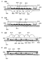
- FIG. 7 illustrates a light-emitting device.
- FIG. 7 illustrates a light-emitting device.
- 5A to 5C illustrate electronic devices.
- 5A to 5C illustrate electronic devices.
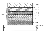
- 5A to 5C illustrate light-emitting elements.
- FIG. 19 shows current density-luminance characteristics of the light-emitting element 1;
- FIG. 16 shows voltage-luminance characteristics of the light-emitting element 1;
- FIG. 16 shows luminance-current efficiency characteristics of the light-emitting element 1;
- FIG. 18 shows voltage-current characteristics of the light-emitting element 1;
- FIG. 16 shows an emission spectrum of the light-emitting element 1;
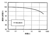
- FIG. 18 shows the reliability of the light-emitting element 1;
- FIG. 19 shows current density-luminance characteristics of the light-emitting element 2;
- FIG. 18 shows voltage-luminance characteristics of the light-emitting element 2.
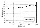
- FIG. 16 shows luminance-current efficiency characteristics of the light-emitting element 2.
- FIG. 18 shows voltage-current characteristics of the light-emitting element 2.
- FIG. 17 shows an emission spectrum of the light-emitting element 2;
- Embodiment 1 an organic compound which is an embodiment of the present invention will be described.
- the organic compound which is one embodiment of the present invention has a pyrene skeleton and is represented by the following general formula (G1).
- Ar represents a substituted or unsubstituted aryl group having 6 to 10 carbon atoms
- ⁇ represents a substituted or unsubstituted phenylene group
- R 1 to R 8 each independently represent And a hydrogen atom, an alkyl group having 1 to 6 carbon atoms, or a substituted or unsubstituted aryl group having 6 to 13 carbon atoms.
- at least one of R 1 to R 8 represents a substituted or unsubstituted aryl group having 6 to 13 carbon atoms.
- R 9 to R 32 each independently represent a hydrogen atom or any one of C 1 to C 6 alkyl groups.
- n is 0 or 1.
- R 1 to R 8 is a substituted or unsubstituted aryl group having 6 to 13 carbon atoms, that is, the pyrene skeleton is substituted or unsubstituted Having an aryl group of 1 to 13 is preferable because the quantum yield of the organic compound represented by General Formula (G1) can be improved.
- Another embodiment of the present invention is an organic compound represented by the following general formula (G2).
- Ar represents a substituted or unsubstituted aryl group having 6 to 10 carbon atoms
- R 1 to R 8 each independently represent a hydrogen atom, an alkyl group having 1 to 6 carbon atoms, or a substituent Or any one of unsubstituted aryl groups having 6 to 13 carbon atoms.
- at least one of R 1 to R 8 represents a substituted or unsubstituted aryl group having 6 to 13 carbon atoms.
- R 9 to R 32 each independently represent a hydrogen atom or any one of C 1 to C 6 alkyl groups.
- R 1 to R 8 is a substituted or unsubstituted aryl group having 6 to 13 carbon atoms, that is, the pyrene skeleton is substituted or unsubstituted Having an aryl group of 1 to 13 is preferable because the quantum yield of the organic compound represented by General Formula (G2) can be improved.
- Another embodiment of the present invention is an organic compound represented by the following general formula (G3).
- Ar represents a substituted or unsubstituted aryl group having 6 to 10 carbon atoms
- R 2 and R 6 each independently represent a hydrogen atom, an alkyl group having 1 to 6 carbon atoms, or a substituent Or any one of unsubstituted aryl groups having 6 to 13 carbon atoms.
- at least one of R 2 and R 6 represents a substituted or unsubstituted aryl group having 6 to 13 carbon atoms.
- R 9 to R 32 each independently represent a hydrogen atom or any one of C 1 to C 6 alkyl groups.
- R 2 and R 6 are a substituted or unsubstituted aryl group having 6 to 13 carbon atoms, that is, a substituted or unsubstituted carbon atom having 6 to 13 carbon atoms in the pyrene skeleton It is preferable because the quantum yield of the organic compound represented by General Formula (G1) can be improved by having the aryl group of
- Another embodiment of the present invention is an organic compound represented by the following general formula (G4).
- R 2 and R 6 each independently represent any one of a hydrogen atom, an alkyl group having 1 to 6 carbon atoms, and a substituted or unsubstituted aryl group having 6 to 13 carbon atoms. However, at least one of R 2 and R 6 represents a substituted or unsubstituted aryl group having 6 to 13 carbon atoms.
- R 9 to R 42 each independently represent a hydrogen atom or any one of C 1 to C 6 alkyl groups.
- R 2 and R 6 are a substituted or unsubstituted aryl group having 6 to 13 carbon atoms, that is, a substituted or unsubstituted carbon atom having 6 to 13 carbon atoms in the pyrene skeleton It is preferable because the quantum yield of the organic compound represented by General Formula (G1) can be improved by having the aryl group of
- R 2 and R 6 are each represented by any one of structural formulas (Ar-1) to (Ar-7) below. It is characterized by
- R 43 to R 97 each independently represent a hydrogen atom or any one of C 1 to C 6 alkyl groups.
- the substituted or unsubstituted aryl group having 6 to 10 carbon atoms has a substituent
- substituents include a methyl group, an ethyl group, a propyl group and an isopropyl group
- Alkyl group having 1 to 7 carbon atoms such as butyl group, isobutyl group, sec-butyl group, tert-butyl group, pentyl group and hexyl group, cyclopentyl group, cyclohexyl group, cycloheptyl group, 8, 9, 10
- cycloalkyl groups having 5 to 7 carbon atoms such as -trinobornanyl group
- aryl groups having 6 to 12 carbon atoms such as a phenyl group, a naphthyl group and a biphenyl group.
- aryl group having 6 to 10 carbon atoms in the general formulas (G1) to (G4) include phenyl group, o-tolyl group, m-tolyl group, p-tolyl group, mesityl group, 1- A naphthyl group, 2-naphthyl group etc. are mentioned.
- alkyl group having 1 to 6 carbon atoms in the general formulas (G1) to (G4) include a methyl group, an ethyl group, a propyl group, an isopropyl group, a butyl group, a sec-butyl group, an isobutyl group, tert-Butyl group, pentyl group, isopentyl group, sec-pentyl group, tert-pentyl group, neopentyl group, hexyl group, isohexyl group, 3-methylpentyl group, 2-methylpentyl group, 2-ethylbutyl group, 1,2 -Dimethylbutyl group, 2,3-dimethylbutyl group, etc. may be mentioned.
- aryl group having 6 to 13 carbon atoms in the general formulas (G1) to (G4) include phenyl group, o-tolyl group, m-tolyl group, p-tolyl group, mesityl group, o- Examples include biphenyl group, m-biphenyl group, p-biphenyl group, 1-naphthyl group, 2-naphthyl group, fluorenyl group, 9,9-dimethylfluorenyl group and the like.
- organic compounds represented by the structural formulas (100) to (128) are examples included in the organic compounds represented by the general formulas (G1) to (G4), and are an aspect of the present invention.
- the organic compound is not limited to this.
- Ar represents a substituted or unsubstituted aryl group having 6 to 10 carbon atoms
- ⁇ represents a substituted or unsubstituted phenylene group
- R 1 to R 8 each independently represent hydrogen It represents an atom, an alkyl group having 1 to 6 carbon atoms, or a substituted or unsubstituted aryl group having 6 to 13 carbon atoms. However, at least one of R 1 to R 8 represents a substituted or unsubstituted aryl group having 6 to 13 carbon atoms.
- R 9 to R 32 each independently represent a hydrogen atom or any one of C 1 to C 6 alkyl groups.
- n is 0 or 1.
- a pyrene derivative (a1) and an amine compound (a2) containing a carbazole skeleton are coupled with a metal catalyst, a metal or a metal compound in the presence of a base
- the organic compound (G1) described in this embodiment can be obtained.
- Ar represents a substituted or unsubstituted aryl group having 6 to 10 carbon atoms
- ⁇ represents a substituted or unsubstituted phenylene group
- R 1 to R 8 each represent Each independently represents a hydrogen atom, an alkyl group having 1 to 6 carbon atoms, or any one of a substituted or unsubstituted aryl group having 6 to 13 carbon atoms.
- at least one of R 1 to R 8 represents a substituted or unsubstituted aryl group having 6 to 13 carbon atoms.
- R 9 to R 32 each independently represent a hydrogen atom or any one of C 1 to C 6 alkyl groups.
- n is 0 or 1.
- X 1 and X 2 each represent a halogen or a triflate group.
- the halogen iodine, bromine or chlorine is preferable.
- a palladium complex or compound such as bis (dibenzylideneacetone) palladium (0) or palladium (II) acetate, tri (tert-butyl) phosphine coordinated thereto, tri (n-hexyl) phosphine,
- a palladium catalyst using a ligand such as tricyclohexyl phosphine is utilized.
- Examples of the base include organic bases such as sodium tert-butoxide and inorganic bases such as potassium carbonate. Moreover, when using a solvent, toluene, xylene, benzene, tetrahydrofuran etc. can be used.
- X 1 and X 2 each represent a halogen.
- the halogen iodine, bromine or chlorine is preferable.
- copper or a copper compound is used as a catalyst.
- R 33 and R 34 in the formula (A-1) each represent a halogen, an acetyl group or the like, and examples of the halogen include chlorine, bromine and iodine.
- Examples of the base to be used include inorganic bases such as potassium carbonate.
- the solvent 1,3-dimethyl-3,4,5,6-tetrahydro-2 (1H) pyrimidinone (DMPU), toluene, xylene, benzene or the like is used.
- DMPU 1,3-dimethyl-3,4,5,6-tetrahydro-2 (1H) pyrimidinone
- the said solvent is not restricted to these.
- DMPU or xylene which has a high boiling point, because the target product can be obtained in a short time and with a high yield when the reaction temperature is 100 ° C. or higher.
- the reaction temperature is more preferably 150 ° C. or higher, DMPU is more preferably used.
- organic compound which is one embodiment of this embodiment can be synthesized.
- the present invention is not limited thereto, and may be synthesized by any other synthetic method. It is good.
- an organic compound having a pyrene skeleton which is one embodiment of the present invention, has a high quantum yield, a light-emitting element, a light-emitting device, an electronic device, a lighting device, or the like having high emission efficiency by using this Can be realized.
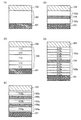
- FIG. 1A shows a light emitting element having an EL layer including a light emitting layer between a pair of electrodes. Specifically, the EL layer 103 is sandwiched between the first electrode 101 and the second electrode 102.
- FIG. 1B a plurality of (two layers in FIG. 1B) EL layers (103a and 103b) are provided between a pair of electrodes, and the charge generation layer 104 is provided between the EL layers.
- 6 shows a light emitting element with a stacked structure (tandem structure). A tandem light emitting element can realize a light emitting device which can be driven at low voltage and consumes low power.
- the charge generation layer 104 injects electrons into one of the EL layers (103a or 103b) and the other of the EL layers (103b or 103a). It has a function of injecting holes. Therefore, in FIG. 1B, when a voltage is applied to the first electrode 101 so that the potential is higher than that of the second electrode 102, electrons are injected from the charge generation layer 104 to the EL layer 103a, and the EL layer 103b is formed. Holes are injected into the
- the charge generation layer 104 is translucent to visible light (specifically, the visible light transmittance of the charge generation layer 104 is 40% or more) from the viewpoint of light extraction efficiency. preferable. In addition, the charge generation layer 104 functions even when the conductivity is lower than that of the first electrode 101 and the second electrode 102.
- FIG. 1C illustrates a stack structure of the EL layer 103 of the light-emitting element which is one embodiment of the present invention.
- the first electrode 101 functions as an anode.
- the EL layer 103 has a structure in which a hole injection layer 111, a hole transport layer 112, a light emitting layer 113, an electron transport layer 114, and an electron injection layer 115 are sequentially stacked on the first electrode 101. Have. Even when a plurality of EL layers are provided as in a tandem structure shown in FIG. 1B, each EL layer is sequentially stacked as described above from the anode side.
- the first electrode 101 is a cathode and the second electrode 102 is an anode, the stacking order is reversed.
- the light-emitting layers 113 included in the EL layers (103, 103a, and 103b) each have a light-emitting substance or a plurality of substances in combination as appropriate, and can be configured to obtain fluorescence or phosphorescence which exhibits a desired emission color. be able to.
- the light emitting layer 113 may have a stacked structure in which light emitting colors are different.
- different materials may be used for the light-emitting substance and the other substances used for the stacked light-emitting layers.
- different emission colors may be obtained from the plurality of EL layers (103a and 103b) illustrated in FIG. 1B.
- different materials may be used as the light-emitting substances and other substances used for the respective light-emitting layers.
- the first electrode 101 shown in FIG. 1C is a reflective electrode
- the second electrode 102 is a semi-transmissive / semi-reflective electrode.
- the (micro cavity) structure With the (micro cavity) structure, light emission obtained from the light emitting layer 113 included in the EL layer 103 can be resonated between the both electrodes, and light emission obtained from the second electrode 102 can be intensified.
- the first electrode 101 of the light emitting element is a reflective electrode having a laminated structure of a reflective conductive material and a light transmissive conductive material (transparent conductive film)
- a film of a transparent conductive film Optical control can be performed by controlling the thickness.
- the inter-electrode distance between the first electrode 101 and the second electrode 102 is near m ⁇ / 2 (where m is a natural number) with respect to the wavelength ⁇ of light obtained from the light emitting layer 113. It is preferable to adjust as follows.
- an optical distance from the first electrode 101 to a region (light emitting region) from which the desired light of the light emitting layer 113 can be obtained is adjusted to be (2 m ′ + 1) ⁇ / 4 (where m ′ is a natural number) It is preferable to do.
- the light emitting region referred to here indicates a recombination region of holes and electrons in the light emitting layer 113.
- the spectrum of specific monochromatic light obtained from the light emitting layer 113 can be narrowed, and light emission with high color purity can be obtained.
- the optical distance between the first electrode 101 and the second electrode 102 may be strictly referred to as the total thickness from the reflective region in the first electrode 101 to the reflective region in the second electrode 102. it can. However, since it is difficult to precisely determine the reflection area of the first electrode 101 and the second electrode 102, it is assumed that an arbitrary position of the first electrode 101 and the second electrode 102 is a reflection area. The above-mentioned effects can be sufficiently obtained.
- the optical distance between the first electrode 101 and the light emitting layer from which desired light is obtained is strictly the optical distance between the reflective region of the first electrode 101 and the light emitting region in the light emitting layer from which desired light is obtained. It can be said that it is a distance.
- any position of the first electrode 101 is a reflective region, Assuming that any position of the light emitting layer from which light is obtained is a light emitting region, the above effect can be sufficiently obtained.
- the light-emitting element illustrated in FIG. 1C has a microcavity structure, light (monochromatic light) having different wavelengths can be extracted even when the light-emitting element has the same EL layer. Therefore, it is not necessary to use different coloring (for example, RGB) to obtain different luminescent colors. Therefore, it is easy to realize high definition. Moreover, the combination with a colored layer (color filter) is also possible. Furthermore, since it becomes possible to intensify the light emission intensity in the front direction of the specific wavelength, it is possible to achieve low power consumption.
- the light-emitting element shown in FIG. 1E is an example of the light-emitting element having a tandem structure shown in FIG. 1B, and as shown in the figure, three EL layers (103a, 103b, 103c) are charge generation layers. It has the structure laminated
- the light emitting layer 113a may be blue, the light emitting layer 113b may be red, green or yellow, and the light emitting layer 113c may be blue, but the light emitting layer 113a may be red and the light emitting layer 113b may be blue, green or yellow Alternatively, the light emitting layer 113c may be red.
- At least one of the first electrode 101 and the second electrode 102 is a light-transmitting electrode (a transparent electrode, a semitransparent / semireflective electrode, or the like) Do.
- the translucent electrode is a transparent electrode
- the visible light transmittance of the transparent electrode is 40% or more.
- the reflectance of visible light of the semi-transmissive and semi-reflective electrode is 20% to 80%, preferably 40% to 70%.
- these electrodes preferably have a resistivity of 1 ⁇ 10 ⁇ 2 ⁇ cm or less.
- the first electrode 101 and the second electrode 102 are reflective electrodes (reflective electrodes)
- visible light of the reflective electrodes The light reflectance is 40% to 100%, preferably 70% to 100%.
- this electrode it is preferable that this electrode have a resistivity of 1 ⁇ 10 ⁇ 2 ⁇ cm or less.
- a specific structure and a manufacturing method of a light-emitting element which is one embodiment of the present invention will be described with reference to FIGS.
- a light emitting element having a tandem structure shown in FIG. 1B and having a microcavity structure is also described with reference to FIG. 1D.
- the first electrode 101 is formed as a reflective electrode
- the second electrode 102 is formed as a semi-transmissive and semi-reflective electrode. Therefore, a desired electrode material can be formed in a single layer or a stack using one or more.
- the second electrode 102 is formed by selecting a material as in the above.
- sputtering or vacuum evaporation can be used to produce these electrodes.
- First electrode and second electrode> As materials for forming the first electrode 101 and the second electrode 102, the following materials can be used in appropriate combination as long as the functions of the two electrodes described above can be satisfied. For example, metals, alloys, electrically conductive compounds, and mixtures thereof can be used as appropriate. Specifically, In-Sn oxide (also referred to as ITO), In-Si-Sn oxide (also referred to as ITSO), In-Zn oxide, and In-W-Zn oxide can be mentioned.
- ITO In-Sn oxide
- ITSO In-Si-Sn oxide
- ITSO In-Zn oxide
- In-W-Zn oxide In-W-Zn oxide
- elements for example, lithium (Li), cesium (Cs), calcium (Ca), strontium (Sr)), europium (Eu), ytterbium, which belong to Group 1 or Group 2 of the periodic table of the elements not illustrated above. It is possible to use rare earth metals such as (Yb) and alloys containing these in combination as appropriate, graphene and the like.
- the hole injecting layer 111a and the hole transporting layer 112a of the EL layer 103a are sequentially formed over the first electrode 101 by a vacuum evaporation method. Layers are formed. After the EL layer 103a and the charge generation layer 104 are formed, the hole injection layer 111b and the hole transport layer 112b of the EL layer 103b are similarly sequentially laminated on the charge generation layer 104.
- the hole injection layer (111, 111a, 111b) is a layer for injecting holes from the first electrode 101 which is an anode or the charge generation layer (104) to the EL layer (103, 103a, 103b). And a layer containing a material having a high hole injection property.
- Materials having high hole injection properties include transition metal oxides such as molybdenum oxide, vanadium oxide, ruthenium oxide, tungsten oxide, and manganese oxide.
- transition metal oxides such as molybdenum oxide, vanadium oxide, ruthenium oxide, tungsten oxide, and manganese oxide.
- phthalocyanine-based compounds such as phthalocyanine (abbr. H 2 Pc) and copper phthalocyanine (abbr .: CuPC); 4,4′-bis [N- (4-diphenylaminophenyl) -N-phenylamino] biphenyl (abbr.
- DPAB N, N'-bis ⁇ 4- [bis (3-methylphenyl) amino] phenyl ⁇ -N, N'-diphenyl- (1,1'-biphenyl) -4,4'-diamine
- An aromatic amine compound such as DNTPD
- a polymer such as poly (3,4-ethylenedioxythiophene) / poly (styrene sulfonic acid) (abbreviation: PEDOT / PSS) can be used.
- a composite material including a hole transporting material and an acceptor property material can also be used as a material having a high hole injection property.
- electrons are extracted from the hole transport material by the acceptor material to generate holes in the hole injection layer (111, 111a, 111b), and the holes are generated through the hole transport layers (112, 112a, 112b). Holes are injected into the light emitting layers (113, 113a, 113b).
- the hole injection layer (111, 111a, 111b) may be formed as a single layer made of a composite material including a hole transporting material and an acceptor material (electron accepting material).
- the material and the acceptor material (electron accepting material) may be stacked in separate layers.
- the hole transport layer (112, 112a, 112b) emits light injected from the first electrode 101 or the charge generation layer (104) by the hole injection layer (111, 111a, 111b) to the light emitting layer (113, 113a, 113b) is a transport layer.
- the hole transport layer (112, 112a, 112b) is a layer containing a hole transport material.
- the hole transporting material used for the hole transporting layer (112, 112a, 112b) in particular, one having a HOMO level equal to or close to the HOMO level of the hole injecting layer (111, 111a, 111b) is used Is preferred.
- an oxide of a metal belonging to Groups 4 to 8 in the periodic table of elements can be used.
- molybdenum oxide, vanadium oxide, niobium oxide, tantalum oxide, chromium oxide, tungsten oxide, manganese oxide, and rhenium oxide can be mentioned.
- molybdenum oxide is particularly preferable because it is stable in the air, has low hygroscopicity, and is easy to handle.
- organic acceptors such as quinodimethane derivatives, chloranil derivatives and hexaazatriphenylene derivatives can be used.
- a hole transporting material used for the hole injection layer (111, 111a, 111b) and the hole transporting layer (112, 112a, 112b) a substance having a hole mobility of 10 -6 cm 2 / Vs or more is used. preferable. Note that materials having hole transportability higher than electrons can be used other than these.
- a ⁇ electron excess heteroaromatic compound for example, carbazole derivative or indole derivative
- an aromatic amine compound is preferable, and as a specific example, 4,4′-bis [N- (1-naphthyl) ) -N-phenylamino] biphenyl (abbreviation: NPB or ⁇ -NPD), N, N′-bis (3-methylphenyl) -N, N′-diphenyl- [1,1′-biphenyl] -4,4 '-Diamine (abbr .: TPD), 4,4'-bis [N- (spiro-9,9'-bifluoren-2-yl) -N-phenylamino] biphenyl (abbr .: BSPB), 4-phenyl-4 '-(9-phenylfluoren-9-yl) triphenylamine (abbreviation: BPAFLP), 4-phenyl-3'-(9-phenyl)
- a compound having a carbazole skeleton, 4,4 ′, 4 ′ ′-(benzene-1,3,5-triyl) tri (dibenzothiophene) (abbreviation: DBT3P-II), 2,8-diphenyl-4- [4-] (9-phenyl-9H-fluoren-9-yl) phenyl] dibenzothiophene (abbreviation: DBTFLP-III), 4- [4- (9-pheny) A compound having a thiophene skeleton such as -9H-fluoren-9-yl) phenyl] -6-phenyldibenzothiophene (abbreviation: DBTFLP-IV), 4,4 ', 4' '-(benzene-1,3,5-benzene) A furan such as triyl) tri (dibenzofuran) (abbreviation: DBF3P-II), 4- ⁇ 3- [3- (9-phenyl-9H-
- poly (N-vinylcarbazole) (abbreviation: PVK)
- TPD Poly- Polymer compounds such as TPD
- the hole transporting material is not limited to the above, and one or more known various materials may be combined to form a hole transporting layer (111, 111a, 111b) and a hole transporting layer as a hole transporting material.
- (112, 112a, 112b) can be used.
- the hole transport layers (112, 112a, 112b) may be formed of a plurality of layers, respectively. That is, for example, the first hole transport layer and the second hole transport layer may be stacked.
- the light emitting layer 113a is formed on the hole transport layer 112a of the EL layer 103a by a vacuum evaporation method. Further, after the EL layer 103a and the charge generation layer 104 are formed, the light emitting layer 113b is formed on the hole transport layer 112b of the EL layer 103b by a vacuum evaporation method.
- the light emitting layer (113, 113a, 113b, 113c) is a layer containing a light emitting substance.
- a substance exhibiting a light-emitting color such as blue, purple, blue-purple, green, yellowish-green, yellow, orange, red and the like is appropriately used.
- different light-emitting colors can be obtained (for example, white light emission obtained by combining light-emitting colors in complementary relationship).
- a stacked structure in which one light emitting layer has different light emitting substances may be employed.
- the light-emitting layer may have one or more kinds of organic compounds (host material, assist material). Further, as the one or more organic compounds, one or both of the hole transporting material and the electron transporting material described in this embodiment can be used.
- a light-emitting substance which can be used for the light-emitting layer 113, 113a, 113b, 113c
- a light-emitting substance which changes singlet excitation energy to light emission in the visible light region, or light emission which changes triplet excitation energy into light emission in the visible light region Substances can be used.
- Examples of light-emitting substances that convert singlet excitation energy into light emission include substances that emit fluorescence (fluorescent materials).
- fluorescent materials include fluorescent materials.
- pyrene derivatives, anthracene derivatives, triphenylene derivatives, fluorene derivatives, carbazole derivatives, dibenzothiophene derivatives, dibenzofuran derivatives, dibenzo Examples include quinoxaline derivatives, quinoxaline derivatives, pyridine derivatives, pyrimidine derivatives, phenanthrene derivatives, naphthalene derivatives and the like. Particularly, pyrene derivatives are preferable because of high emission quantum yield.
- pyrene derivatives include N, N'-bis (3-methylphenyl) -N, N'-bis [3- (9-phenyl-9H-fluoren-9-yl) phenyl] pyrene-1,6. -Diamine (abbreviation: 1,6mMemFLPAPrn), N, N'-diphenyl-N, N'-bis [4- (9-phenyl-9H-fluoren-9-yl) phenyl] pyrene-1,6-diamine (abbreviation) N, N'-bis (dibenzofuran-2-yl) -N, N'-diphenylpyrene-1,6-diamine (abbreviation: 1,6 FrAPrn), N, N'-bis (dibenzothiophene) -2-yl) -N, N'-diphenylpyrene-1,6-diamine (abbreviation: 1,6ThAPrn), N, N '-bis
- a substance that emits phosphorescence (phosphorescent material) and thermally activated delayed fluorescence (TADF) material that exhibits thermally activated delayed fluorescence can be mentioned.
- Examples of the phosphorescent material include organic metal complexes, metal complexes (platinum complexes), and rare earth metal complexes. Since these exhibit different emission colors (emission peaks) for each substance, they are appropriately selected and used as needed.
- a phosphorescent material which exhibits blue or green and has a peak wavelength of emission spectrum of 450 nm or more and 570 nm or less, the following substances may be mentioned.
- a phosphorescent material which exhibits a green or yellow color and has a peak wavelength of emission spectrum of 495 nm or more and 590 nm or less, the following substances can be mentioned.
- tris (4-methyl-6-phenylpyrimidinato) iridium (III) (abbreviation: [Ir (mppm) 3 ]
- tris (4-t-butyl-6-phenylpyrimidinato) iridium (III) (Abbreviation: [Ir (tBuppm) 3 ])
- (acetylacetonato) bis (6-methyl-4-phenylpyrimidinato) iridium (III) abbreviation: [Ir (mppm) 2 (acac)]
- Acetylacetonato) bis (6-tert-butyl-4-phenylpyrimidinato) iridium (III) (abbreviation: [Ir (tBuppm) 2 (acac)]
- (acetylacetonato) bis [6- (2- (2-) Norbornyl) -4-phenylpyrimidinato] iridium (III) (abbreviation: [Ir
- a phosphorescent material which exhibits yellow or red and has a peak wavelength of 570 nm or more and 750 nm or less in the light emission spectrum, the following substances may be mentioned.
- organic compounds (host materials and assist materials) used for the light emitting layer (113, 113a, 113b, 113c) one or plural kinds of substances having energy gaps larger than the energy gap of the light emitting substance (guest material) are selected It may be used.
- a compound which forms an exciplex with a phosphorescent substance it is preferable to use a compound which forms an exciplex with a phosphorescent substance. Note that, with such a configuration, light emission using ExTET (Exciplex-Triplet Energy Transfer), which is energy transfer from an exciplex to a light-emitting substance, can be obtained.
- ExTET Exciplex-Triplet Energy Transfer
- various organic compounds can be appropriately combined and used, but in order to efficiently form an excited complex, a compound that easily receives holes (hole transportable material) and a compound that easily receives electrons (electrons It is particularly preferred to combine with a transportable material).
- the light-emitting substance is a fluorescent material
- an anthracene derivative or a tetracene derivative it is preferable to use an anthracene derivative or a tetracene derivative.
- an organic compound whose triplet excitation energy is larger than the triplet excitation energy of the light-emitting substance (the energy difference between the ground state and the triplet excited state) may be selected as the host material.
- the host material in addition to zinc and aluminum metal complexes, oxadiazole derivatives, triazole derivatives, benzimidazole derivatives, quinoxaline derivatives, dibenzoquinoxaline derivatives, dibenzothiophene derivatives, dibenzofuran derivatives, pyrimidine derivatives, triazine derivatives, pyridine derivatives
- aromatic amines and carbazole derivatives can be used.
- the following hole transporting materials and electron transporting materials can be used as the host material.
- Examples of the host material having a high hole transportability include N, N′-di (p-tolyl) -N, N′-diphenyl-p-phenylenediamine (abbreviation: DTDPPA), 4,4′-bis [4] N- (4-diphenylaminophenyl) -N-phenylamino] biphenyl (abbreviation: DPAB), N, N'-bis ⁇ 4- [bis (3-methylphenyl) amino] phenyl ⁇ -N, N'-diphenyl -(1,1'-biphenyl) -4,4'-diamine (abbreviation: DNTPD), 1,3,5-tris [N- (4-diphenylaminophenyl) -N-phenylamino] benzene (abbreviation: DPA3B) Etc. can be mentioned.
- DTDPPA N′-di (p-tolyl) -N, N′-dipheny
- PCzDPA1 3- [N- (4-diphenylaminophenyl) -N-phenylamino] -9-phenylcarbazole
- PCzDPA2 3,6-bis [N- (4-diphenylaminophenyl) -N-phenyl Amino] -9-phenylcarbazole
- PCzTPN2 3, 6-bis [N- (4-diphenylaminophenyl) -N- (1-naphthyl) amino] -9-phenylcarbazole
- PCzTPN2 3 -[N- (9-phenylcarbazol-3-yl) -N-phenylamino] -9-phenylcarbazole
- PCzPCA1 3,6-bis [N- (9-phenylcarbazol-3-yl)- N-phenylamino] -9-phenylcarbazole
- PCzPCA1 3,6-bis [N- (9-phenylcarbazol-3
- NPB or ⁇ -NPD 4,4′-bis [N- (1-naphthyl) -N-phenylamino] biphenyl
- NPB or ⁇ -NPD N, N ′ -Bis (3-methylphenyl) -N, N'-diphenyl- [1,1'-biphenyl] -4,4'-diamine
- TPD 4,4 ', 4' '-tris (carbazole-) 9-yl) triphenylamine
- TCTA 4,4 ′, 4 ′ ′-tris [N- (1-naphthyl) -N-phenylamino] triphenylamine
- 1′-TNATA 4 4,4 ′, 4 ′ ′-tris (N, N-diphenylamino) triphenylamine
- TPD 4,4′, 4 ′ ′-tris [N- (1-naphthyl) -N-phenylamino]
- PCPN 3- [4- (1-naphthyl) -phenyl] -9-phenyl-9H-carbazole
- PCPPn 3- [4- (9-phenanthryl) -phenyl] -9-phenyl-9H-carbazole
- PCCP 3,3'-bis (9-phenyl-9H-carbazole)
- mCP 1,3-bis (N-carbazolyl) benzene
- CzTP 3, 6-bis ( 3,5-Diphenylphenyl) -9-phenylcarbazole
- a host material having high electron transportability for example, tris (8-quinolinolato) aluminum (III) (abbreviation: Alq), tris (4-methyl-8-quinolinolato) aluminum (III) (abbreviation: Almq 3 ), bis (10-hydroxybenzo [h] quinolinato) beryllium (II) (abbreviation: BeBq 2 ), bis (2-methyl-8-quinolinolato) (4-phenylphenolato) aluminum (III) (abbreviation: BAlq), bis (b 8-quinolinolato) zinc (II) (abbreviation: Znq) and the like, metal complexes having a quinoline skeleton or a benzoquinoline skeleton, and the like.
- Alq bis (10-hydroxybenzo [h] quinolinato) beryllium
- BeBq 2 bis (2-methyl-8-quinolinolato) (4-phenylphenolato) aluminum
- BAlq bis (b
- bis [2- (2-benzoxazolyl) phenolato] zinc (II) (abbreviation: ZnPBO), bis [2- (2-benzothiazolyl) phenolato] zinc (II) (abbreviation: ZnBTZ), etc.
- ZnPBO bis [2- (2-benzoxazolyl) phenolato] zinc
- ZnBTZ bis [2- (2-benzothiazolyl) phenolato] zinc
- a metal complex having an oxazole type or thiazole type ligand can also be used.
- 2- (4-biphenylyl) -5- (4-tert-butylphenyl) -1,3,4-oxadiazole (abbreviation: PBD), 1,3-bis [5 -(P-tert-butylphenyl) -1,3,4-oxadiazol-2-yl] benzene (abbreviation: OXD-7), 9- [4- (5-phenyl-1,3,4-oxa] Oxadiazole derivatives such as diazol-2-yl) phenyl] -9H-carbazole (abbreviation: CO11) or 3- (4-biphenylyl) -4-phenyl-5- (4-tert-butylphenyl)- Triazole derivatives such as 1,2,4-triazole (abbreviation: TAZ) or 2,2 ′, 2 ′ ′-(1,3,5-benzenetriyl) tris (1-phenyl-1H-benzimid
- poly (2,5-pyridinediyl) (abbreviation: PPy)
- poly [(9,9-dihexylfluorene-2,7-diyl) -co- (pyridine-3,5-diyl)] (abbreviation: PF -Py)
- PF -BPy poly [(9,9-dioctyl fluorene-2,7-diyl) -co- (2,2'-bipyridine-6,6'-diyl)]
- fused polycyclic aromatic compounds such as anthracene derivatives, phenanthrene derivatives, pyrene derivatives, chrysene derivatives, dibenzo [g, p] chrysene derivatives and the like can be mentioned.
- 9,10-diphenylanthracene Abbreviations: DP Anth
- N, N-diphenyl-9- [4- (10-phenyl-9-anthryl) phenyl] -9H-carbazol-3-amine abbreviation: CzA1PA
- 4- (10-phenyl-9-) Anthryl) triphenylamine abbreviation: DPhPA
- YGAPA PCAPA
- N, 9-diphenyl-N- ⁇ 4- [4- (10-phenyl-9-anthryl) phenyl] phenyl ⁇ -9H-carbazol-3-amine Abbreviation: PCAPBA
- 2PCAPA 6,12-dimethoxy-5,11-diphenyl Lysene
- DBC1 9- [4- (10-phenyl-9-anthracenyl) phenyl] -9H-carbazole
- CzPA 3,6-diphenyl-9- [4- (10-
- the light emitting layer When a plurality of organic compounds are used in the light emitting layer (113, 113a, 113b, 113c), two kinds of compounds (first and second compounds) forming an exciplex are mixed with an organic metal complex. You may use it.
- various organic compounds can be appropriately combined and used, but in order to efficiently form an excited complex, a compound that easily receives holes (hole transportable material) and a compound that easily receives electrons (electrons It is particularly preferred to combine with a transportable material).
- the hole transporting material and the electron transporting material the materials described in this embodiment can be used. By this configuration, high efficiency, low voltage and long life can be realized simultaneously.
- TADF material refers to a material that can up-convert a triplet excited state to a singlet excited state with slight thermal energy (reverse intersystem crossing) and efficiently exhibit light emission (fluorescence) from the singlet excited state. is there.
- the energy difference between the triplet excitation level and the singlet excitation level is 0 eV or more and 0.2 eV or less, preferably 0 eV or more and 0.1 eV or less It can be mentioned.
- the delayed fluorescence in the TADF material refers to light emission having a remarkably long life while having the same spectrum as normal fluorescence. The lifetime is 10 -6 seconds or more, preferably 10 -3 seconds or more.
- TADF materials include fullerene and derivatives thereof, acridine derivatives such as proflavin, eosin and the like.
- metal-containing porphyrins including magnesium (Mg), zinc (Zn), cadmium (Cd), tin (Sn), platinum (Pt), indium (In), palladium (Pd) and the like can be mentioned.
- metal-containing porphyrin examples include protoporphyrin-tin fluoride complex (abbreviation: SnF 2 (Proto IX)), mesoporphyrin-tin fluoride complex (abbreviation: SnF 2 (Meso IX)), hematoporphyrin-tin fluoride Complex (abbreviation: SnF 2 (Hemato IX)), coproporphyrin tetramethyl ester-tin fluoride complex (abbreviation: SnF 2 (Copro III-4Me)), octaethyl porphyrin-tin fluoride complex (abbreviation: SnF 2 (OEP) ), Ethioporphyrin-tin fluoride complex (abbreviation: SnF 2 (Etio I)), octaethylporphyrin-platinum chloride complex (abbreviation: PtCl 2 OEP), and the like.
- a heterocycle having a ⁇ electron excess heteroaromatic ring and a ⁇ electron deficient heteroaromatic ring Compounds can be used.
- the substance in which the ⁇ electron excess heteroaromatic ring and the ⁇ electron deficiency heteroaromatic ring are directly bonded has both the donor property of the ⁇ electron excess heteroaromatic ring and the acceptor activity of the ⁇ electron deficiency heteroaromatic ring. It is particularly preferable because the energy difference between the singlet excited state and the triplet excited state is reduced.
- TADF material when using a TADF material, it can also be used in combination with another organic compound.
- the electron transporting layer 114a is formed on the light emitting layer 113a of the EL layer 103a by vacuum evaporation.
- the electron transport layer 114b is formed on the light emitting layer 113b of the EL layer 103b by a vacuum evaporation method.
- the electron transport layer (114, 114a, 114b) emits light injected from the second electrode 102 or the charge generation layer (104) by the electron injection layer (115, 115a, 115b) to the light emitting layer (113, 113a, 113b).
- the electron transporting material used for the electron transporting layer (114, 114a, 114b) is preferably a substance having an electron mobility of 1 ⁇ 10 ⁇ 6 cm 2 / Vs or more. Note that materials that can transport electrons more than holes can be used.
- Electron transport materials include metal complexes having quinoline ligands, benzoquinoline ligands, oxazole ligands, or thiazole ligands, oxadiazole derivatives, triazole derivatives, phenanthroline derivatives, pyridine derivatives, bipyridine derivatives, etc. Can be mentioned.
- ⁇ electron deficient heteroaromatic compounds such as nitrogen-containing heteroaromatic compounds can also be used.
- Alq 3 tris (4-methyl-8-quinolinolato) aluminum (abbreviation: Almq 3 ), bis (10-hydroxybenzo [h] quinolinato) beryllium (abbreviation: BeBq 2 ), BAlq, bis [2 -(2-hydroxyphenyl) benzoxazolato] zinc (II) (abbreviation: Zn (BOX) 2 ), bis [2- (2- hydroxyphenyl) benzothiazolato] zinc (abbreviation: Zn (BTZ) 2 ), etc.
- poly (2,5-pyridinediyl) (abbreviation: PPy)
- poly [(9,9-dihexylfluorene-2,7-diyl) -co- (pyridine-3,5-diyl)] (abbreviation: PF -Py)
- PF -BPy poly [(9,9-dioctyl fluorene-2,7-diyl) -co- (2,2'-bipyridine-6,6'-diyl)]
- the electron-transporting layer (114, 114a, 114b) is not limited to a single layer, and may have a structure in which two or more layers containing the above substances are stacked.
- the electron injection layer 115a is formed on the electron transport layer 114a of the EL layer 103a by vacuum evaporation. Thereafter, the EL layer 103a and the charge generation layer 104 are formed, and the electron transport layer 114b of the EL layer 103b is formed, and then the electron injection layer 115b is formed thereon by a vacuum evaporation method.
- the electron injection layer (115, 115a, 115b) is a layer containing a substance having a high electron injection property.
- an alkali metal such as lithium fluoride (LiF), cesium fluoride (CsF), calcium fluoride (CaF 2 ), lithium oxide (LiO x ), etc.
- alkali Earth metals or compounds thereof can be used.
- a rare earth metal compound such as erbium fluoride (ErF 3 ) can be used.
- electride may be used for the electron injection layer (115, 115a, 115b). Examples of electride include a substance in which electrons are added to a mixed oxide of calcium and aluminum at a high concentration, and the like.
- the substance which comprises the electron carrying layer (114, 114a, 114b) mentioned above can also be used.
- a composite material formed by mixing an organic compound and an electron donor (donor) may be used for the electron injection layer (115, 115a, 115b).
- a composite material is excellent in electron injectability and electron transportability because electrons are generated in the organic compound by the electron donor.
- the organic compound is preferably a material excellent in transporting generated electrons, and specifically, for example, an electron transporting material (metal complex used for the electron transporting layer (114, 114a, 114b) described above And heteroaromatic compounds etc. can be used.
- the electron donor any substance may be used as long as it exhibits an electron donating property to the organic compound.
- alkali metals, alkaline earth metals and rare earth metals are preferable, and lithium, cesium, magnesium, calcium, erbium, ytterbium and the like can be mentioned.
- alkali metal oxides and alkaline earth metal oxides are preferable, and lithium oxide, calcium oxide, barium oxide and the like can be mentioned.
- Lewis bases such as magnesium oxide can be used.
- an organic compound such as tetrathiafulvalene (abbreviation: TTF) can also be used.
- the optical distance between the second electrode 102 and the light emitting layer 113 b is less than ⁇ / 4 with respect to the wavelength of light exhibited by the light emitting layer 113 b. It is preferable to form so that In this case, the thickness can be adjusted by changing the film thickness of the electron transport layer 114 b or the electron injection layer 115 b.
- the charge generation layer 104 injects electrons into the EL layer 103a and holes in the EL layer 103b. It has a function to inject.
- the charge generation layer 104 has a configuration in which an electron acceptor (acceptor) is added to a hole transport material, or a configuration in which an electron donor (donor) is added to an electron transport material. Good. Also, both of these configurations may be stacked. Note that by forming the charge generation layer 104 using the above-described material, an increase in driving voltage in the case where the EL layers are stacked can be suppressed.
- the material described in this embodiment can be used as the hole transport material.
- the electron acceptor include 7,7,8,8-tetracyano-2,3,5,6-tetrafluoroquinodimethane (abbreviation: F 4 -TCNQ), chloranil and the like.
- oxides of metals belonging to Groups 4 to 8 of the periodic table can be given. Specifically, vanadium oxide, niobium oxide, tantalum oxide, chromium oxide, molybdenum oxide, tungsten oxide, manganese oxide, rhenium oxide and the like can be mentioned.
- the material described in this embodiment can be used as the electron transport material.
- the electron donor an alkali metal, an alkaline earth metal, a rare earth metal, a metal belonging to Groups 2 and 13 of the periodic table, or an oxide or carbonate thereof can be used.
- lithium (Li), cesium (Cs), magnesium (Mg), calcium (Ca), ytterbium (Yb), indium (In), lithium oxide, cesium carbonate or the like is preferably used.
- an organic compound such as tetrathianaphthacene may be used as the electron donor.
- the EL layer 103c in FIG. 1E may have a structure similar to that of the above-described EL layers (103, 103a, and 103b).
- the charge generation layers 104 a and 104 b may have the same configuration as the charge generation layer 104 described above.
- the light-emitting elements described in this embodiment can be formed over various substrates.
- substrate is not limited to a specific thing.
- the substrate include a semiconductor substrate (for example, a single crystal substrate or a silicon substrate), an SOI substrate, a glass substrate, a quartz substrate, a plastic substrate, a metal substrate, a stainless steel still substrate, a substrate having a stainless steel foil, a tungsten substrate, A substrate having a tungsten foil, a flexible substrate, a laminated film, a paper containing a fibrous material, or a base film may be mentioned.
- barium borosilicate glass, alumino borosilicate glass, soda lime glass etc. are mentioned as an example of a glass substrate.
- a synthetic material such as plastic represented by polyethylene terephthalate (PET), polyethylene naphthalate (PEN), polyether sulfone (PES), acrylic, etc.
- PET polyethylene terephthalate
- PEN polyethylene naphthalate
- PES polyether sulfone
- acrylic acrylic
- Resin, polypropylene, polyester, polyvinyl fluoride, or polyvinyl chloride, polyamide, polyimide, aramid, epoxy, inorganic vapor deposition film, papers, etc. are mentioned.
- a vacuum process such as an evaporation method or a solution process such as a spin coating method or an inkjet method can be used for manufacturing the light-emitting element described in this embodiment.
- vapor deposition physical vapor deposition (PVD) such as sputtering, ion plating, ion beam deposition, molecular beam deposition, vacuum deposition, chemical vapor deposition (CVD) or the like is used. be able to.
- PVD physical vapor deposition
- CVD chemical vapor deposition
- functional layers hole injection layers (111, 111a, 111b), hole transport layers (112, 112a, 112b), light emitting layers (113, 113a, 113b, 113c), and electron transport included in the EL layer of the light emitting device)
- a vapor deposition method vacuum vapor deposition method etc.
- a coating method dip coat method
- Die coating method bar coating method
- spin coating method spray coating method
- printing method in jet method, screen (stencil printing) method, offset (planographic printing) method, flexo (letterpress printing) method, gravure method, micro contact It can form by methods, such as a method etc.).
- a high molecular compound oligomer, dendrimer, polymer etc.
- a medium molecular compound compound of intermediate region of low molecule and high molecule: molecular weight 400 to 4000
- inorganic compound quantum dot material etc.
- the quantum dot material a colloidal quantum dot material, an alloy quantum dot material, a core / shell quantum dot material, a core quantum dot material, or the like can be used.
- a light-emitting device which is one embodiment of the present invention will be described.
- active matrix light emission in which a transistor (FET) 202 on a first substrate 201 and a light-emitting element (203R, 203G, 203B, 203W) are electrically connected to each other
- the plurality of light emitting elements (203R, 203G, 203B, 203W) have a common EL layer 204, and the optical distance between the electrodes of each light emitting element is different according to the light emitting color of each light emitting element. It has a tuned microcavity structure.
- it is a top emission type light emitting device in which light emission obtained from the EL layer 204 is emitted through the color filters (206R, 206G, and 206B) formed on the second substrate 205.
- the light-emitting device illustrated in FIG. 2A is formed to function as the first electrode 207 as a reflective electrode.
- the second electrode 208 is formed to function as a semi-transmissive and semi-reflective electrode. Note that an electrode material for forming the first electrode 207 and the second electrode 208 may be appropriately used with reference to the description of the other embodiments.
- the light emitting element 203R is a red light emitting element
- the light emitting element 203G is a green light emitting element
- the light emitting element 203B is a blue light emitting element
- the light emitting element 203W is a white light emitting element
- the light emitting element 203R is adjusted so that the optical distance 200R is between the first electrode 207 and the second electrode 208
- the light emitting element 203G includes the first electrode 207 and the second electrode.
- the light distance between the light emitting element 203B and the second electrode 208 is adjusted to be an optical distance 200B. Note that as shown in FIG.
- the conductive layer 210R is stacked on the first electrode 207
- the conductive layer 210G is stacked on the first electrode 207
- color filters (206R, 206G, and 206B) are formed on the second substrate 205.
- the color filter is a filter that passes a specific wavelength range of visible light and blocks the specific wavelength range. Therefore, as shown in FIG. 2A, red light emission can be obtained from the light emitting element 203R by providing the color filter 206R which passes only the red wavelength region at a position overlapping with the light emitting element 203R. Further, by providing the color filter 206G which passes only the green wavelength region at a position overlapping with the light emitting element 203G, green light emission can be obtained from the light emitting element 203G.
- blue light emission can be obtained from the light emitting element 203B by providing the color filter 206B that allows only the blue wavelength range to pass through at a position overlapping with the light emitting element 203B.
- the light emitting element 203W can obtain white light emission without providing a color filter.
- a black layer (black matrix) 209 may be provided at an end of one type of color filter.
- the color filters (206R, 206G, 206B) and the black layer 209 may be covered with an overcoat layer using a transparent material.
- FIG. 2A shows a light emitting device having a structure (top emission type) for emitting light to the second substrate 205 side
- the light-emitting device may have a structure (bottom emission type) in which light is extracted to the side 201.
- the first electrode 207 is formed to function as a semi-transmissive and semi-reflective electrode
- the second electrode 208 is formed to function as a reflective electrode.
- the first substrate 201 uses at least a light-transmitting substrate.
- the color filters (206R ′, 206G ′, and 206B ′) may be provided closer to the first substrate 201 than the light-emitting elements (203R, 203G, and 203B) as illustrated in FIG. 2C.
- FIG. 2A shows the case where the light-emitting element is a red light-emitting element, a green light-emitting element, a blue light-emitting element, or a white light-emitting element
- the light-emitting element of one embodiment of the present invention is limited to that structure.
- a yellow light emitting element or an orange light emitting element may be provided.
- an EL layer a light emitting layer, a hole injection layer, a hole transport layer, an electron transport layer, an electron injection layer, a charge generation layer, etc.
- other embodiments It may be used as appropriate with reference to the description of In that case, it is also necessary to appropriately select a color filter in accordance with the light emission color of the light emitting element.
- Embodiment 4 In this embodiment mode, a light-emitting device which is one embodiment of the present invention will be described.
- an active matrix light-emitting device or a passive matrix light-emitting device can be manufactured.
- an active matrix light-emitting device has a structure in which a light-emitting element and a transistor (FET) are combined. Therefore, both passive matrix light-emitting devices and active matrix light-emitting devices are included in one embodiment of the present invention.
- the light-emitting element described in any of the other embodiments can be applied to the light-emitting device described in this embodiment.
- an active matrix light-emitting device is described with reference to FIG.
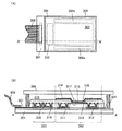
- FIG. 3A is a top view of the light emitting device
- FIG. 3B is a cross-sectional view of FIG. 3A taken along a dashed line A-A '.
- the active matrix light-emitting device includes a pixel portion 302, a driver circuit portion (source line driver circuit) 303, and driver circuit portions (gate line driver circuits) (304a and 304b) provided over a first substrate 301. .
- the pixel portion 302 and the driver circuit portions (303, 304 a, 304 b) are sealed between the first substrate 301 and the second substrate 306 by the sealant 305.
- a lead wiring 307 is provided over the first substrate 301.
- the lead wiring 307 is connected to the FPC 308 which is an external input terminal.
- the FPC 308 transmits signals (eg, video signals, clock signals, start signals, reset signals, and the like) and potentials from the outside to the driver circuit units (303, 304a, and 304b).
- a printed wiring board (PWB) may be attached to the FPC 308. Note that the state in which the FPC or the PWB is attached is included in the light emitting device.
- the pixel portion 302 is formed of a plurality of pixels including a FET (switching FET) 311, an FET (current control FET) 312, and a first electrode 313 electrically connected to the FET 312. Note that the number of FETs included in each pixel is not particularly limited, and can be appropriately set as needed.
- the FETs 309, 310, 311, and 312 are not particularly limited, and, for example, transistors such as a staggered transistor or an inverted staggered transistor can be applied. In addition, a top gate type or bottom gate type transistor structure may be employed.
- the crystallinity of the semiconductor that can be used for these FETs 309, 310, 311, and 312 is not particularly limited, and an amorphous semiconductor, a semiconductor having crystallinity (a microcrystalline semiconductor, a polycrystalline semiconductor, a single crystal semiconductor, Alternatively, any of semiconductors each having a crystal region in part may be used. Note that using a semiconductor having crystallinity is preferable because deterioration of transistor characteristics can be suppressed.
- an element of Group 14 a compound semiconductor, an oxide semiconductor, an organic semiconductor, or the like can be used.
- a semiconductor containing silicon, a semiconductor containing gallium arsenide, an oxide semiconductor containing indium, or the like can be used.
- the driver circuit portion 303 includes an FET 309 and an FET 310.
- the FET 309 and the FET 310 may be formed by a circuit including a unipolar (N-type or P-type) transistor, or may be formed by a CMOS circuit including an N-type transistor and a P-type transistor. It is good.
- a driver circuit may be provided outside.
- the end of the first electrode 313 is covered with an insulator 314.
- an organic compound such as a negative photosensitive resin or a positive photosensitive resin (acrylic resin), or an inorganic compound such as silicon oxide, silicon oxynitride, or silicon nitride can be used.
- the insulator 314 preferably has a curved surface having a curvature at the upper end or the lower end. Thereby, the coverage of the film formed in the upper layer of the insulator 314 can be made favorable.
- the EL layer 315 and a second electrode 316 are stacked over the first electrode 313.
- the EL layer 315 includes a light emitting layer, a hole injecting layer, a hole transporting layer, an electron transporting layer, an electron injecting layer, a charge generation layer, and the like.
- the structure and materials described in the other embodiments can be applied to the structure of the light-emitting element 317 described in this embodiment.
- the second electrode 316 is electrically connected to the FPC 308 which is an external input terminal.
- light emitting element 317 Although only one light emitting element 317 is illustrated in the cross-sectional view in FIG. 3B, a plurality of light emitting elements are arranged in a matrix in the pixel portion 302. Light-emitting elements which can emit light of three types (R, G, and B) can be selectively formed in the pixel portion 302, so that a light-emitting device capable of full-color display can be formed. In addition to light emitting elements that can obtain three types (R, G, B) of light emissions, light emissions such as white (W), yellow (Y), magenta (M), cyan (C), etc. An element may be formed.
- a light emitting element capable of obtaining the above-described several types of light emission to a light emitting element capable of obtaining three types of light emission (R, G, B)
- effects such as improvement of color purity and reduction of power consumption can be obtained.
- a light emitting device capable of full color display may be provided by combining with a color filter.
- red (R), green (G), blue (B), cyan (C), magenta (M), yellow (Y) etc. can be used as a kind of color filter.
- the FETs (309, 310, 311, and 312) and the light emitting element 317 on the first substrate 301 are attached to each other with the sealant 305 so that the second substrate 306 and the first substrate 301 are bonded to each other.
- a structure provided in a space 318 surrounded by the second substrate 301 and the sealing material 305 is provided.
- the space 318 may be filled with an inert gas (such as nitrogen or argon) or an organic substance (including the sealant 305).
- the sealing material 305 an epoxy resin or glass frit can be used. Note that for the sealing material 305, it is preferable to use a material that does not transmit moisture or oxygen as much as possible.
- the second substrate 306 a substrate which can be used for the first substrate 301 can be used similarly. Therefore, various substrates described in the other embodiments can be used as appropriate.
- the substrate other than a glass substrate and a quartz substrate, a plastic substrate made of FRP (Fiber-Reinforced Plastics), PVF (polyvinyl fluoride), polyester, acrylic, or the like can be used.
- FRP Fiber-Reinforced Plastics
- PVF polyvinyl fluoride
- polyester acrylic, or the like
- an active matrix light-emitting device can be obtained.
- the FET and the light-emitting element may be formed directly on the flexible substrate, but the FET and the light-emitting element may be formed over another substrate having a peeling layer. After that, the FET and the light emitting element may be separated by a peeling layer by applying heat, force, laser irradiation or the like, and may be further transferred to a flexible substrate.
- the peeling layer for example, a lamination of an inorganic film of a tungsten film and a silicon oxide film, an organic resin film such as polyimide, or the like can be used.
- a flexible substrate in addition to a substrate capable of forming a transistor, a paper substrate, a cellophane substrate, an aramid film substrate, a polyimide film substrate, a cloth substrate (natural fiber (silk, cotton, linen), synthetic fiber ( Examples include nylon, polyurethane, polyester) or regenerated fibers (including acetate, cupra, rayon, regenerated polyester), leather substrates, rubber substrates and the like.
- a substrate capable of forming a transistor, a paper substrate, a cellophane substrate, an aramid film substrate, a polyimide film substrate, a cloth substrate (natural fiber (silk, cotton, linen), synthetic fiber ( Examples include nylon, polyurethane, polyester) or regenerated fibers (including acetate, cupra, rayon, regenerated polyester), leather substrates, rubber substrates and the like.
- the electronic devices illustrated in FIGS. 4A to 4E include a housing 7000, a display portion 7001, a speaker 7003, an LED lamp 7004, an operation key 7005 (including a power switch or an operation switch), a connection terminal 7006, Sensor 7007 (force, displacement, position, velocity, acceleration, angular velocity, rotation number, distance, light, liquid, magnetism, temperature, chemical substance, voice, time, hardness, electric field, current, voltage, electric power, radiation, flow rate, humidity (Including the function of measuring inclination, vibration, smell, or infrared light), a microphone (microphone) 7008, and the like.
- Sensor 7007 force, displacement, position, velocity, acceleration, angular velocity, rotation number, distance, light, liquid, magnetism, temperature, chemical substance, voice, time, hardness, electric field, current, voltage, electric power, radiation, flow rate, humidity (Including the function of measuring inclination, vibration, smell, or infrared light), a microphone (microphone) 7008, and the like.
- FIG. 4A illustrates a mobile computer, which can include a switch 7009, an infrared port 7010, and the like in addition to the above components.
- FIG. 4B shows a portable image reproducing apparatus (for example, a DVD reproducing apparatus) provided with a recording medium, which may have a second display portion 7002, a recording medium reading portion 7011, and the like in addition to those described above. it can.
- a portable image reproducing apparatus for example, a DVD reproducing apparatus
- a recording medium which may have a second display portion 7002, a recording medium reading portion 7011, and the like in addition to those described above. it can.
- FIG. 4C illustrates a goggle type display, which can include a second display portion 7002, a support portion 7012, an earphone 7013, and the like in addition to the above components.
- FIG. 4D illustrates a digital camera with a television receiving function, which can include an antenna 7014, a shutter button 7015, an image receiving unit 7016, and the like in addition to the above components.
- FIG. 4E illustrates a mobile phone (including a smartphone).
- the housing 7000 can include the display portion 7001, the microphone 7019, the speaker 7003, the camera 7020, the external connection portion 7021, an operation button 7022, and the like. .
- FIG. 4F illustrates a large television set (also referred to as a television or a television receiver), which can include the housing 7000, the display portion 7001, and the like. Further, here, a structure in which the housing 7000 is supported by the stand 7018 is shown.
- the television set can be operated by a separate remote control 7111 or the like.
- the display portion 7001 may be provided with a touch sensor, or may be operated by touching the display portion 7001 with a finger or the like.
- the remote controller 7111 may have a display unit for displaying information output from the remote controller 7111. Channels and volume can be controlled with an operation key or a touch panel included in the remote controller 7111, and an image displayed on the display portion 7001 can be manipulated.
- the electronic devices illustrated in FIG. 4A to FIG. 4F can have various functions. For example, a function to display various information (still images, moving images, text images, etc.) on the display unit, a touch panel function, a calendar, a function to display date or time, etc., a function to control processing by various software (programs) Wireless communication function, function to connect to various computer networks using wireless communication function, function to transmit or receive various data using wireless communication function, read out a program or data recorded in a recording medium
- a function to display on the display portion can be provided.
- the function of displaying image information mainly on one display unit and displaying character information mainly on another display unit or considering parallax in a plurality of display units It is possible to have a function of displaying a three-dimensional image and the like by displaying the captured image. Furthermore, in an electronic device having an image receiving unit, the function of capturing a still image, the function of capturing a moving image, the function of automatically or manually correcting the captured image, the captured image in a recording medium (externally or built in a camera) A function to save, a function to display a captured image on a display portion, and the like can be provided. Note that the electronic devices illustrated in FIGS. 4A to 4F can have various functions without limitation to the above.
- FIG. 4G illustrates a smart watch, which includes a housing 7000, a display portion 7001, operation buttons 7022 and 7023, a connection terminal 7024, a band 7025, a clasp 7026, and the like.
- the display portion 7001 mounted in a housing 7000 which also serves as a bezel portion has a non-rectangular display area.
- the display portion 7001 can display an icon 7027 indicating time, another icon 7028, and the like.
- the display unit 7001 may be a touch panel (input / output device) on which a touch sensor (input device) is mounted.
- the smart watch illustrated in FIG. 4G can have various functions. For example, a function to display various information (still images, moving images, text images, etc.) on the display unit, a touch panel function, a calendar, a function to display date or time, etc., a function to control processing by various software (programs) Wireless communication function, function to connect to various computer networks using wireless communication function, function to transmit or receive various data using wireless communication function, read out a program or data recorded in a recording medium A function to display on the display portion can be provided.
- a function to display various information still images, moving images, text images, etc.
- a touch panel function a calendar
- a function to display date or time etc.
- a function to control processing by various software (programs) Wireless communication function function to connect to various computer networks using wireless communication function
- function to transmit or receive various data using wireless communication function read out a program or data recorded in a recording medium
- a function to display on the display portion can be provided.
- a speaker inside the housing 7000, a speaker, a sensor (force, displacement, position, velocity, acceleration, angular velocity, rotation number, distance, light, liquid, magnetism, temperature, chemical substance, voice, time, hardness, electric field, current Voltage, power, radiation, flow rate, humidity, inclination, vibration, odor or infrared (including the function of measuring infrared), a microphone, and the like.
- a sensor force, displacement, position, velocity, acceleration, angular velocity, rotation number, distance, light, liquid, magnetism, temperature, chemical substance, voice, time, hardness, electric field, current Voltage, power, radiation, flow rate, humidity, inclination, vibration, odor or infrared (including the function of measuring infrared), a microphone, and the like.
- the light-emitting device which is one embodiment of the present invention and the display device including the light-emitting element which is one embodiment of the present invention can be used for each display portion of the electronic device described in this embodiment and has long lifetime. Can be realized.
- FIG. 5A shows a portable information terminal 9310 in a developed state.
- FIG. 5B shows the portable information terminal 9310 in the middle of changing from one of the expanded state or the folded state to the other.
- FIG. 5C shows a portable information terminal 9310 in a folded state.
- the portable information terminal 9310 is excellent in portability in the folded state, and in the expanded state, is excellent in viewability of display due to a wide seamless display area.
- the display portion 9311 is supported by three housings 9315 connected by hinges 9313.
- the display portion 9311 may be a touch panel (input / output device) on which a touch sensor (input device) is mounted.
- the display portion 9311 can be reversibly deformed into a folded state from the expanded state by bending the space between the two housings 9315 through the hinges 9313.
- the light-emitting device of one embodiment of the present invention can be used for the display portion 9311.
- a long-life electronic device can be realized.
- a display area 9312 in the display portion 9311 is a display area located on the side surface of the portable information terminal 9310 in a folded state. An information icon, a frequently used application, a shortcut of a program, and the like can be displayed in the display area 9312, and information confirmation and activation of the application and the like can be performed smoothly.
- the present invention can be applied to the light 5101 (including the rear of the vehicle body) outside the automobile shown in FIG. 6A, the wheel 5102 of the tire, part or all of the door 5103, and the like. Further, the present invention can be applied to the display 5104, the handle 5105, the shift lever 5106, the seat 5107, the inner rear view mirror 5108, and the like inside the automobile shown in FIG. 6B. In addition, you may apply to a part of glass window.
- an electronic device or a car to which the light-emitting device or the display device which is one embodiment of the present invention is applied can be obtained. In that case, a long-life electronic device can be realized.
- applicable electronic devices and vehicles are not limited to those described in this embodiment, and can be applied in any field.
- FIGS. 7C and 7D show an example of a cross-sectional view of the lighting device.
- 7A and 7B illustrate bottom emission type light emitting devices that extract light to the substrate side
- FIGS. 7C and 7D illustrate top emission type light emitting devices that extract light to the sealing substrate side. It is a lighting device.
- the lighting device 4000 illustrated in FIG. 7A includes the light emitting element 4002 over the substrate 4001.
- a substrate 4003 having unevenness is provided outside the substrate 4001.
- the light-emitting element 4002 includes a first electrode 4004, an EL layer 4005, and a second electrode 4006.
- the first electrode 4004 is electrically connected to the electrode 4007, and the second electrode 4006 is electrically connected to the electrode 4008.
- an auxiliary wiring 4009 electrically connected to the first electrode 4004 may be provided.
- an insulating layer 4010 is formed over the auxiliary wiring 4009.
- the substrate 4001 and the sealing substrate 4011 are attached to each other by a sealing material 4012.
- a desiccant 4013 is preferably provided between the sealing substrate 4011 and the light emitting element 4002. Note that since the substrate 4003 has unevenness as illustrated in FIG. 7A, the light extraction efficiency of the light-emitting element 4002 can be improved.
- a diffusion plate 4015 may be provided outside the substrate 4001 as in the lighting device 4100 in FIG. 7B.
- the lighting device 4200 in FIG. 7C includes a light emitting element 4202 over a substrate 4201.
- the light emitting element 4202 has a first electrode 4204, an EL layer 4205, and a second electrode 4206.
- the first electrode 4204 is electrically connected to the electrode 4207, and the second electrode 4206 is electrically connected to the electrode 4208.
- an auxiliary wiring 4209 electrically connected to the second electrode 4206 may be provided.
- an insulating layer 4210 may be provided below the auxiliary wiring 4209.
- the substrate 4201 and the sealing substrate 4211 with unevenness are attached with a sealant 4212.
- a barrier film 4213 and a planarization film 4214 may be provided between the sealing substrate 4211 and the light emitting element 4202. Note that the sealing substrate 4211 has unevenness as illustrated in FIG. 7C, so that the light extraction efficiency of the light-emitting element 4202 can be improved.
- a diffusion plate 4215 may be provided over the light emitting element 4202 as in the lighting device 4300 in FIG. 7D.
- a lighting device which is one embodiment of the present invention or a light-emitting element which is a part of the light-emitting device, a lighting device having a desired chromaticity can be provided.
- the ceiling light 8001 has a ceiling direct attachment type and an in-ceiling type. Note that such a lighting device is configured by combining a light emitting device with a housing or a cover. In addition, application to a cord pendant type (cord hanging type from a ceiling) is also possible.
- the foot lamp 8002 can illuminate the floor surface to enhance the safety of the foot.
- it is effective to use for a bedroom, a stairs, a passage, etc.
- the size and shape can be changed as appropriate according to the size and structure of the room.
- it is also possible to set it as the stationary type illuminating device comprised combining a light-emitting device and a support stand.
- the sheet-like illumination 8003 is a thin sheet-like illumination device. It can be used for a wide range of applications without taking up space because it is used by being attached to a wall. In addition, it is easy to increase the area. In addition, it can also be used for the wall surface and case which have a curved surface.
- a lighting device 8004 in which light from a light source is controlled only in a desired direction can also be used.
- a lighting device having a function as furniture and can do.
- N, N′-bis (9-phenyl-9H-carbazol-3-yl) -3 which is an organic compound according to one embodiment of the present invention, which is represented by Structural Formula (100) in Embodiment 1.
- a synthesis method of 1,8-diphenyl-N, N'-di (m-tolyl) -1,6-pyrenediamine (abbreviation: ph-1, 6mMePCAPrn) is described. The structure of ph-1, 6mMePCAPrn is shown below.
- an ultraviolet-visible absorption spectrum (hereinafter simply referred to as “absorption spectrum”) and an emission spectrum of ph-1,6mMePCAPrn in a toluene solution are shown in FIG.
- the horizontal axis represents wavelength
- the vertical axis represents absorption intensity and emission intensity.
- An ultraviolet-visible spectrophotometer (V550 manufactured by JASCO Corporation) was used for measurement of the absorption spectrum.
- the absorption spectrum of ph-1,6mMePCAPrn in a toluene solution is obtained by measuring toluene in a quartz cell from the absorption spectrum obtained by measuring the toluene solution of ph-1,6mMePCAPrn in a quartz cell. It was calculated by subtracting the absorption spectrum.
- a fluorometer (FS920 manufactured by Hamamatsu Photonics K.K.) was used to measure the emission spectrum.
- the emission spectrum of ph-1,6mMePCAPrn in a toluene solution was measured by placing the toluene solution of ph-1,6mMePCAPrn in a quartz cell.
- the absorption spectrum and the emission spectrum of the solid thin film of ph-1, 6mMePCAPrn were measured.
- the solid thin film was produced on a quartz substrate by vacuum evaporation.
- the absorption spectrum of the thin film was calculated from the absorbance including the substrate and the absorbance (-log10 [% T / (100-% R)] determined from the reflectance, where% T is the transmittance, and% R is the reflection.
- the UV-visible spectrophotometer U-4100, manufactured by Hitachi High-Technologies Corporation
- the fluorospectrometer manufactured by Hamamatsu Photonics, FS920
- the measurement results of the absorption spectrum and the emission spectrum of the obtained solid thin film are shown in Fig. 10 (B)
- the horizontal axis represents wavelength
- the vertical axis represents absorption intensity and emission intensity.
- the organic compound ph-1, 6mMePCAPrn which is one embodiment of the present invention can also be used as a host of a light-emitting substance or a fluorescent substance in a visible region.
- the thin film of ph-1, 6mMePCAPrn had stable film quality even under the atmosphere.
- the absolute quantum yield of ph-1, 6mMePCAPrn was measured.
- the measurement of the absolute quantum yield is carried out by using an absolute PL quantum yield measurement apparatus (C9920-02 manufactured by Hamamatsu Photonics Co., Ltd., C9920-02), using toluene as a solvent, and then measuring at a room temperature in the wavelength range of 400 nm to 500 nm. Did. As a result, it was found that the absolute quantum yield was 90% and high luminous efficiency was exhibited.
- the absolute quantum yield of 1, 6 PCAPrn was similarly measured as a comparative material, and the absolute quantum yield was 80%. Therefore, it was found that ph-1,6mMePCAPrn has a high absolute quantum yield due to having a phenyl group as an aryl group in the pyrene skeleton as compared to 1,6PCAPrn.
- N, N′-bis (9-phenyl-9H-carbazol-3-yl) -3 which is an organic compound according to one embodiment of the present invention, which is represented by Structural Formula (101) in Embodiment 1.
- a synthesis method of 1,8-diphenyl-N, N'-di (3,5-xylyl) -1,6-pyrenediamine (abbreviation: ph-1, 6DMePCAPrn) is described.
- the structural formula of ph-1, 6DMePCAPrn is shown below.
- FIG. 1 An absorption spectrum and an emission spectrum of ph-1,6DMePCAPrn in a toluene solution are shown in FIG.
- the horizontal axis represents wavelength
- the vertical axis represents absorption intensity and emission intensity.
- An ultraviolet-visible spectrophotometer (V550 manufactured by JASCO Corporation) was used for measurement of the absorption spectrum.
- the absorption spectrum of ph-1,6DMePCAPrn in a toluene solution is obtained by measuring toluene in a quartz cell from the absorption spectrum obtained by measuring the toluene solution of ph-1,6DMePCAPrn in a quartz cell. It was calculated by subtracting the absorption spectrum.
- a fluorometer (FS920 manufactured by Hamamatsu Photonics K.K.) was used to measure the emission spectrum.
- the emission spectrum of ph-1,6DMePCAPrn in a toluene solution was measured by placing the toluene solution of ph-1,6DMePCAPrn in a quartz cell.
- the absorption spectrum and the emission spectrum of the solid thin film of ph-1, 6DMePCAPrn were measured.
- the solid thin film was produced on a quartz substrate by vacuum evaporation.
- the absorption spectrum of the thin film was calculated from the absorbance including the substrate and the absorbance (-log10 [% T / (100-% R)] determined from the reflectance, where% T is the transmittance, and% R is the reflection.
- the UV-visible spectrophotometer U-4100, manufactured by Hitachi High-Technologies Corporation
- the fluorospectrometer manufactured by Hamamatsu Photonics, FS920
- the measurement results of the absorption spectrum and the emission spectrum of the obtained solid thin film are shown in Fig. 12 (B)
- the horizontal axis represents wavelength
- the vertical axis represents absorption intensity and emission intensity.
- ph-1, 6DMePCAPrn emits green light.
- the organic compound ph-1, 6DMePCAPrn which is one embodiment of the present invention can also be used as a host of a light-emitting substance or a fluorescent substance in a visible region.
- the thin film of ph-1, 6DMePCAPrn had stable film quality even under the atmosphere.
- the HOMO and LUMO levels of ph-1, 6DMePCAPrn were calculated based on cyclic voltammetry (CV) measurement. The calculation method is shown below.
- an electrochemical analyzer manufactured by BAS Co., Ltd., model number: ALS model 600A or 600C was used.
- the solution in the CV measurement uses dehydrated dimethylformamide (DMF) (99.8%, catalog number: 22705-6, manufactured by Aldrich Co., Ltd.) as a solvent, and tetra-n-butylammonium perchlorate (supporting electrolyte) n-Bu 4 NClO 4 ) (manufactured by Tokyo Chemical Industry Co., Ltd., catalog number; T0836) is dissolved to a concentration of 100 mmol / L, and the measurement target is further dissolved to a concentration of 2 mmol / L. did.
- a platinum electrode manufactured by BAS Co., Ltd., PTE platinum electrode
- a platinum electrode A manufactured by BAS Inc., a Pt counter electrode for VC-3 (manufactured by BAS Inc.) as an auxiliary electrode 5 cm
- an Ag / Ag + electrode manufactured by BAS Co., Ltd., RE7 non-aqueous solvent-based reference electrode
- the measurement was performed at room temperature (20 or more and 25 degrees C or less).
- the scanning speed at the time of CV measurement was unified to 0.1 V / sec, and the oxidation potential Ea [V] and the reduction potential Ec [V] with respect to the reference electrode were measured.
- Ea was an intermediate potential of the oxidation-reduction wave
- Ec was an intermediate potential of the reduction-oxidation wave.
- the HOMO level [eV] ⁇ 4.94-Ea
- CV measurement was repeated 100 times, and the oxidation-reduction wave in the 100th cycle measurement was compared with the oxidation-reduction wave in the first cycle to examine the electrical stability of the compound.
- the absolute quantum yield of ph-1, 6DMePCAPrn was measured.
- the measurement of the absolute quantum yield is carried out by using an absolute PL quantum yield measurement apparatus (C9920-02 manufactured by Hamamatsu Photonics Co., Ltd., C9920-02), using toluene as a solvent, and then measuring at a room temperature in the wavelength range of 400 nm to 500 nm. Did. As a result, it was found that the absolute quantum yield was 88% and high luminous efficiency was shown.
- the absolute quantum yield of 1, 6 PCAPrn was similarly measured as a comparative material, and the absolute quantum yield was 80%. Therefore, it was found that ph-1,6DMePCAPrn has a high absolute quantum yield due to having a phenyl group as an aryl group in the pyrene skeleton as compared to 1,6PCAPrn.
- a light emitting element which is one embodiment of the present invention
- the element structure of the light emitting element used in this embodiment is shown in FIG. 13 and its specific configuration is shown in Table 1.
- chemical formulas of materials used in this example are shown below.
- the light emitting element shown in this embodiment includes a hole injecting layer 911, a hole transporting layer 912, a light emitting layer 913 as a light emitting layer 902 on a first electrode 901 formed on a substrate 900 as shown in FIG.
- the electron transporting layer 914 and the electron injecting layer 915 are sequentially stacked, and the second electrode 903 is stacked on the electron injecting layer 915.
- the first electrode 901 was formed over the substrate 900.
- the electrode area was 4 mm 2 (2 mm ⁇ 2 mm).
- a glass substrate was used for the substrate 900.
- the first electrode 901 was formed by depositing indium tin oxide containing silicon oxide (ITSO) to a thickness of 70 nm by a sputtering method.
- ITSO indium tin oxide containing silicon oxide
- the surface of the substrate was washed with water, baked at 200 ° C. for 1 hour, and subjected to UV ozone treatment for 370 seconds.
- the substrate is introduced into a vacuum deposition apparatus whose inside is depressurized to about 10 -4 Pa, and vacuum baking is performed at 170 ° C. for 30 minutes in a heating chamber in the vacuum deposition apparatus, and then the substrate is released for about 30 minutes. It was cold.
- the hole injecting layer 911 was formed over the first electrode 901.
- the hole injection layer 911 is 3- [4- (9-phenanthryl) phenyl] -9-phenyl-9H-carbazole (abbreviation: PCPPn) and molybdenum oxide.
- PCPPn 3- [4- (9-phenanthryl) phenyl] -9-phenyl-9H-carbazole
- molybdenum oxide 4: 2 (mass ratio).
- the hole transport layer 912 was formed on the hole injection layer 911.
- the hole transport layer 912 was formed by vapor deposition using PCPPn so as to have a thickness of 30 nm.
- the light emitting layer 913 was formed over the hole transporting layer 912.
- the electron transporting layer 914 was formed over the light emitting layer 913.
- the electron-transporting layer 914 was formed by sequential evaporation so that the film thickness of 2ph-cgDBCzPA was 10 nm, and the film thickness of bathophenanthroline (abbreviation: Bphen) was 15 nm.
- the electron injection layer 915 was formed over the electron transport layer 914.
- the electron injection layer 915 was formed by evaporation using lithium fluoride (LiF) so as to have a thickness of 1 nm.
- a second electrode 903 was formed over the electron injection layer 915.
- the second electrode 903 was formed by depositing aluminum to a thickness of 200 nm.
- the second electrode 903 functions as a cathode.
- a light-emitting element in which an EL layer is sandwiched between a pair of electrodes is formed over the substrate 900.
- the hole injecting layer 911, the hole transporting layer 912, the light emitting layer 913, the electron transporting layer 914, and the electron injecting layer 915 described in the above steps are functional layers which form the EL layer in one embodiment of the present invention.
- all vapor deposition methods using resistance heating were used.
- the light emitting element manufactured as described above is sealed by another substrate (not shown).
- another substrate (not shown) coated with a sealant that solidifies with ultraviolet light is placed on the substrate 900 in a glove box under a nitrogen atmosphere.
- the substrates were fixed so that the sealant was attached around the light emitting element formed on the substrate 900.
- the sealing agent was solidified by irradiating ultraviolet light of 365 nm at 6 J / cm 2, and the sealing agent was stabilized by heat treatment at 80 ° C. for 1 hour.
- Operation characteristics of light emitting element >> The operating characteristics of the manufactured light emitting element 1 were measured. In addition, the measurement was performed at room temperature. Further, as a result of the operation characteristics of the light emitting element 1, FIG. 14 shows current density-luminance characteristics, FIG. 15 shows voltage-luminance characteristics, FIG. 16 shows luminance-current efficiency characteristics, and FIG.
- Table 2 shows initial values of main characteristics of the light-emitting element 1 at around 1000 cd / m 2.
- the light-emitting element 1 manufactured in this example exhibits a good efficiency.
- FIG. 18 a light emission spectrum when a current is supplied to the light-emitting element 1 at a current density of 12.5 mA / cm 2 is shown in FIG.
- the emission spectrum of the light-emitting element 1 has a peak at around 516 nm, which is suggested to be derived from the emission of ph ⁇ 1, 6 mMePCAPrn contained in the light-emitting layer 913.
- the reliability test performed the constant current drive test which supplied the fixed electric current by the current density of 50 mA / cm ⁇ 2 >.
- a light emitting element 2 using ph-1, 6DMePCAPrn (structural formula (101)) described in Example 2 for a light emitting layer is manufactured, and the characteristics thereof The measured results are shown.
- the light-emitting element 2 shown in this example was manufactured in the same manner as the light-emitting element 1 shown in Example 3 from the first electrode 901 to the hole transport layer 912.
- the electron transporting layer 914 was formed over the light emitting layer 913.
- the electron-transporting layer 914 was formed by sequential evaporation so that the film thickness of cgDBCzPA was 15 nm and the film thickness of bathophenanthroline (abbreviation: Bphen) was 10 nm.
- FIG. 20 shows current density-luminance characteristics of the light-emitting element 2
- FIG. 21 shows voltage-luminance characteristics
- FIG. 22 shows luminance-current efficiency characteristics
- FIG. 23 shows voltage-current characteristics.
- the light-emitting element 2 manufactured in this example shows a good efficiency.
- FIG. 24 A light emission spectrum when a current is supplied to the light-emitting element 2 at a current density of 12.5 mA / cm 2 is shown in FIG. As shown in FIG. 24, the emission spectrum of the light-emitting element has a peak at around 520 nm, which is suggested to be derived from the emission of ph-1, 6DMePCAPrn contained in the light-emitting layer 913.
- 101 first electrode, 102: second electrode, 103: EL layer, 103a, 103b, 103c: EL layer, 104 (104a, 104b): charge generation layer, 111, 111a, 111b: hole injection layer, 112, 112a, 112b: hole transport layer, 113, 113a, 113b: light emitting layer, 114, 114a, 114b: electron transport layer, 115, 115a, 115b: electron injection layer, 200R, 200G, 200B: optical distance, 201 First substrate, 202: transistor (FET), 203R, 203G, 203B, 203W: light emitting element, 204: EL layer, 205: second substrate, 206R, 206G, 206B: color filter, 206R ', 206G' , 206 B ′: color filter, 207: first electrode, 208: second electrode, 209: black layer Matrix), 210R, 210G: conductive layer, 301:
Landscapes
- Chemical & Material Sciences (AREA)
- Organic Chemistry (AREA)
- Engineering & Computer Science (AREA)
- Physics & Mathematics (AREA)
- Materials Engineering (AREA)
- Spectroscopy & Molecular Physics (AREA)
- General Physics & Mathematics (AREA)
- Theoretical Computer Science (AREA)
- Optics & Photonics (AREA)
- Electroluminescent Light Sources (AREA)
- Indole Compounds (AREA)
- Devices For Indicating Variable Information By Combining Individual Elements (AREA)
Abstract
Description
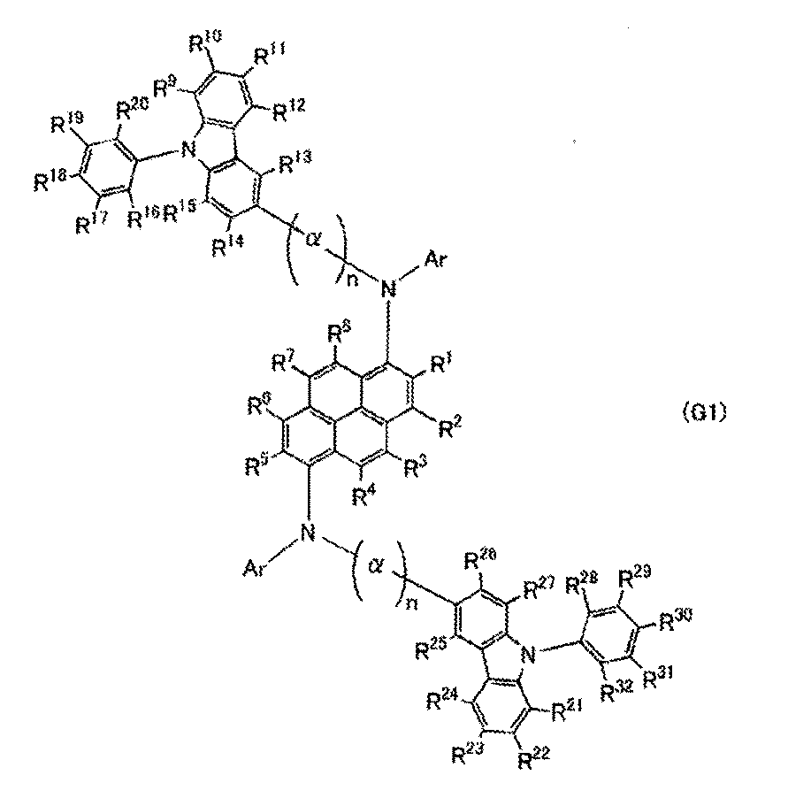

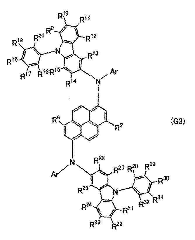
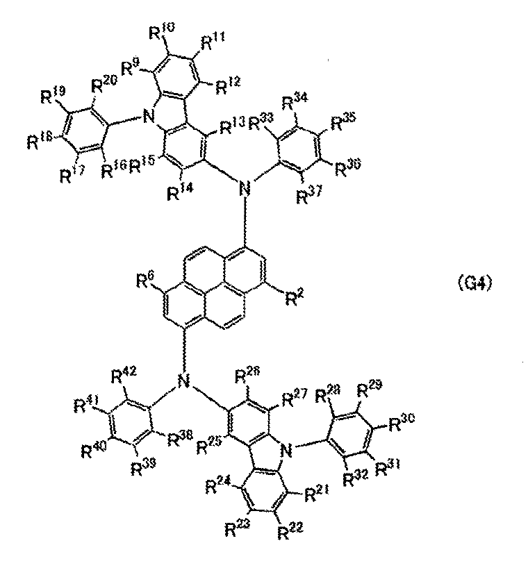
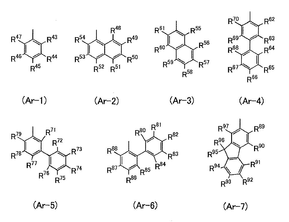
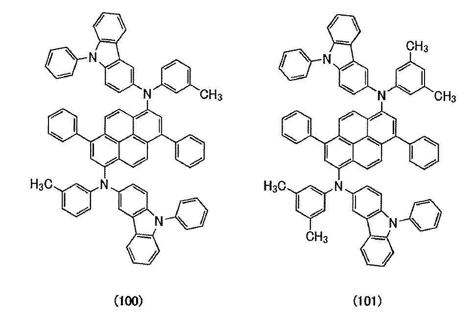
本実施の形態では、本発明の一態様である有機化合物について説明する。なお、本発明の一態様である有機化合物は、ピレン骨格を有し、下記一般式(G1)で表される。
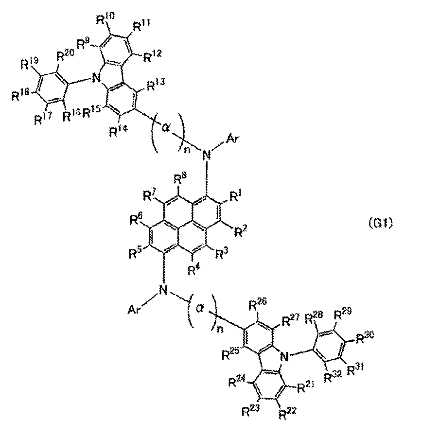


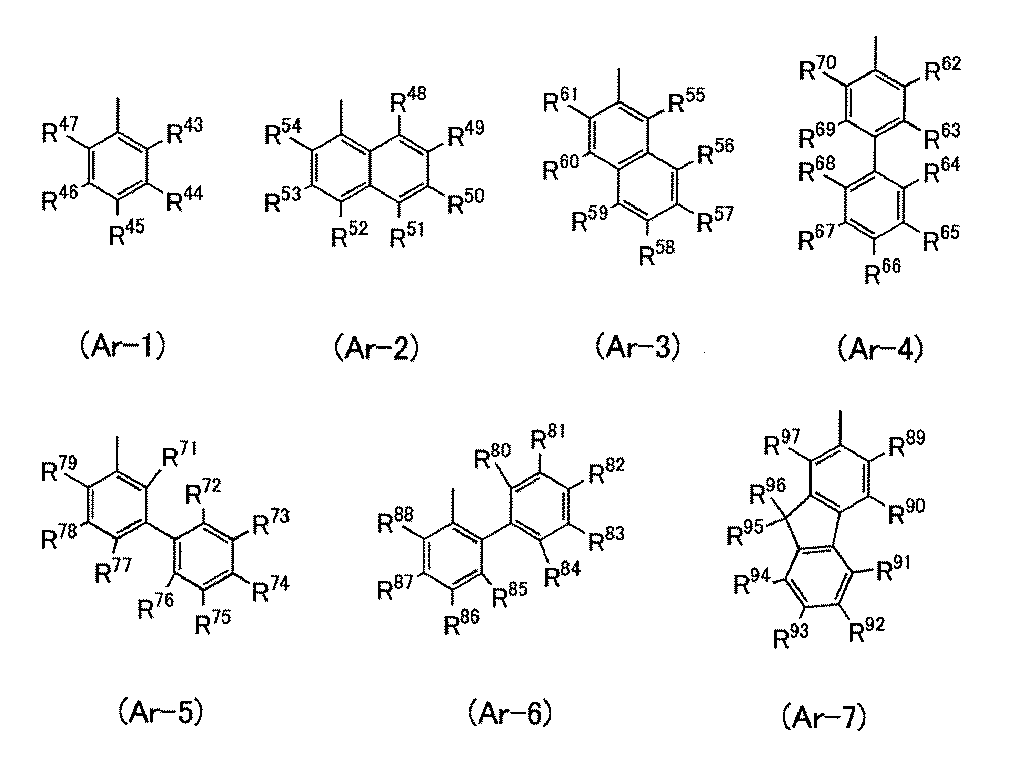
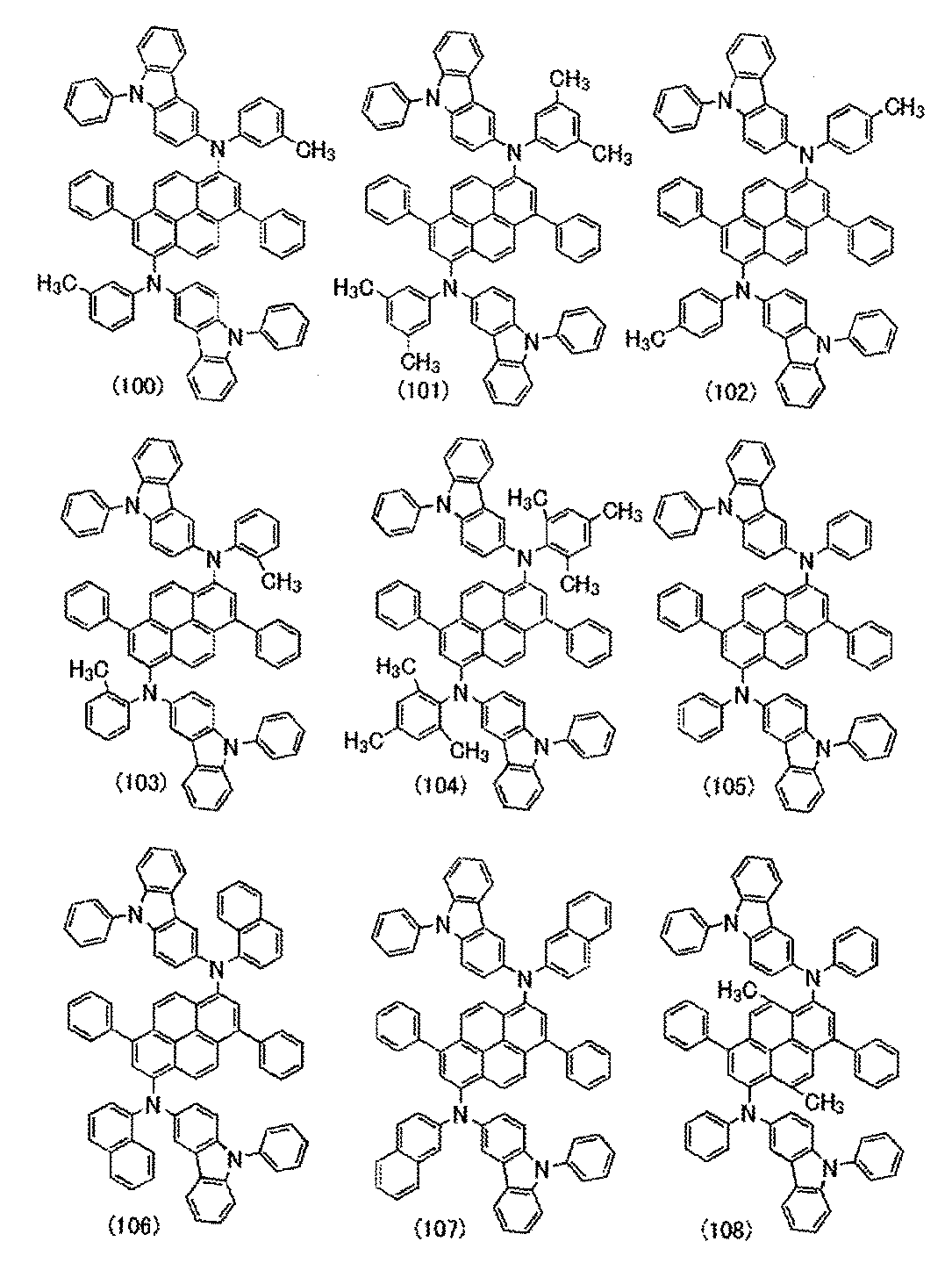
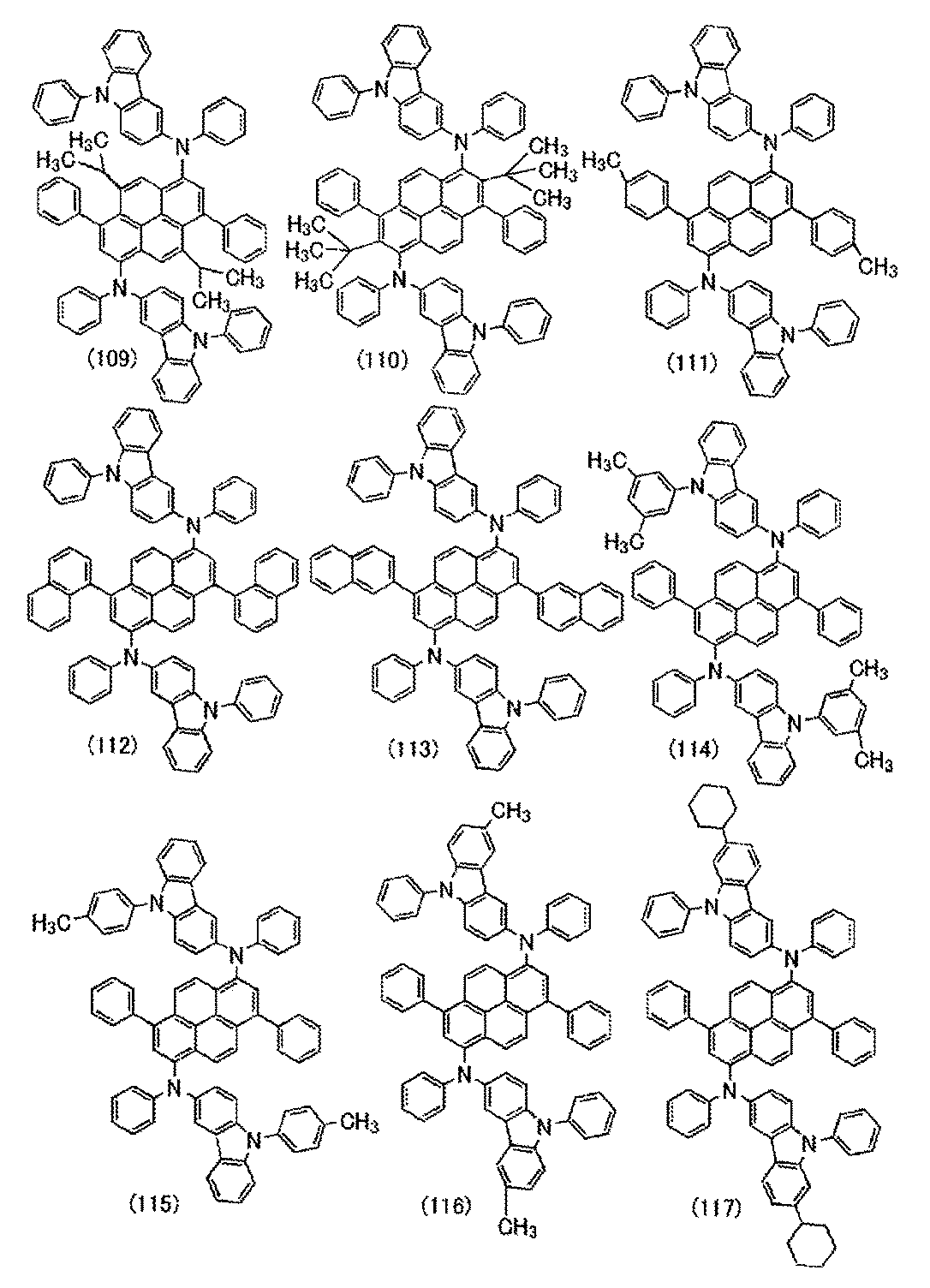

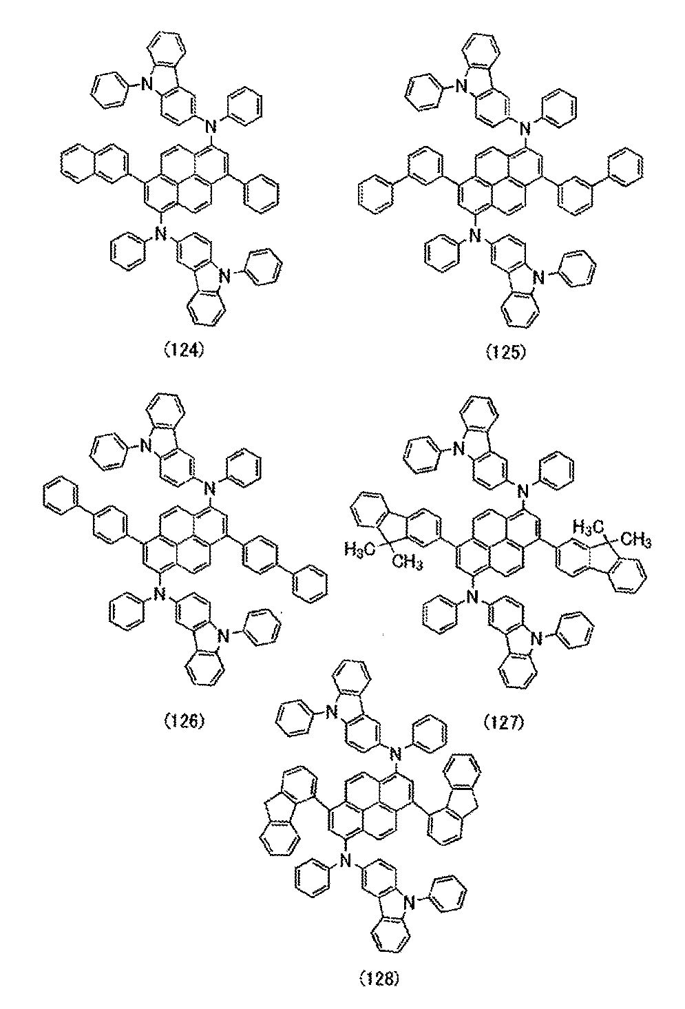

上記一般式(G1)で表される有機化合物の合成には、種々の反応を適用することができ、例えば、以下の合成スキームに示す簡便な方法により、一般式(G1)で表される有機化合物を合成することができる。
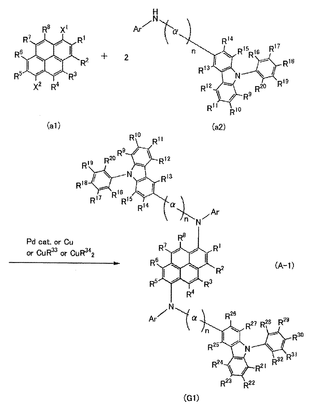
本実施の形態では、実施の形態1で示した有機化合物を用いた発光素子について図1を用いて説明する。
まず、発光素子の基本的な構造について説明する。図1(A)には、一対の電極間に発光層を含むEL層を有する発光素子を示す。具体的には、第1の電極101と第2の電極102との間にEL層103が挟まれた構造を有する。
次に、本発明の一態様である発光素子の具体的な構造および作製方法について、図1を用いて説明する。また、ここでは、図1(B)に示すタンデム構造を有し、マイクロキャビティ構造を備えた発光素子についても図1(D)を用いて説明する。図1(D)に示す発光素子がマイクロキャビティ構造を有する場合は、第1の電極101を反射電極として形成し、第2の電極102を半透過・半反射電極として形成する。従って、所望の電極材料を単数または複数用い、単層または積層して形成することができる。なお、第2の電極102は、EL層103bを形成した後、上記と同様に材料を選択して形成する。また、これらの電極の作製には、スパッタ法や真空蒸着法を用いることができる。
第1の電極101および第2の電極102を形成する材料としては、上述した両電極の機能が満たせるのであれば、以下に示す材料を適宜組み合わせて用いることができる。例えば、金属、合金、電気伝導性化合物、およびこれらの混合物などを適宜用いることができる。具体的には、In−Sn酸化物(ITOともいう)、In−Si−Sn酸化物(ITSOともいう)、In−Zn酸化物、In−W−Zn酸化物が挙げられる。その他、アルミニウム(Al)、チタン(Ti)、クロム(Cr)、マンガン(Mn)、鉄(Fe)、コバルト(Co)、ニッケル(Ni)、銅(Cu)、ガリウム(Ga)、亜鉛(Zn)、インジウム(In)、スズ(Sn)、モリブデン(Mo)、タンタル(Ta)、タングステン(W)、パラジウム(Pd)、金(Au)、白金(Pt)、銀(Ag)、イットリウム(Y)、ネオジム(Nd)などの金属、およびこれらを適宜組み合わせて含む合金を用いることもできる。その他、上記例示のない元素周期表の第1族または第2族に属する元素(例えば、リチウム(Li)、セシウム(Cs)、カルシウム(Ca)、ストロンチウム(Sr))、ユウロピウム(Eu)、イッテルビウム(Yb)などの希土類金属およびこれらを適宜組み合わせて含む合金、その他グラフェン等を用いることができる。
正孔注入層(111、111a、111b)は、陽極である第1の電極101や電荷発生層(104)からEL層(103、103a、103b)に正孔(ホール)を注入する層であり、正孔注入性の高い材料を含む層である。
発光層(113、113a、113b、113c)は、発光物質を含む層である。なお、発光物質としては、青色、紫色、青紫色、緑色、黄緑色、黄色、橙色、赤色などの発光色を呈する物質を適宜用いる。また、複数の発光層(113a、113b、113c)に異なる発光物質を用いることにより異なる発光色を呈する構成(例えば、補色の関係にある発光色を組み合わせて得られる白色発光)とすることができる。さらに、一つの発光層が異なる発光物質を有する積層構造であっても良い。
電子輸送層(114、114a、114b)は、電子注入層(115、115a、115b)によって、第2の電極102や電荷発生層(104)から注入された電子を発光層(113、113a、113b)に輸送する層である。なお、電子輸送層(114、114a、114b)は、電子輸送性材料を含む層である。電子輸送層(114、114a、114b)に用いる電子輸送性材料は、1×10⁻⁶cm2/Vs以上の電子移動度を有する物質が好ましい。なお、正孔よりも電子の輸送性の高い物質であれば、これら以外のものを用いることができる。
電子注入層(115、115a、115b)は、電子注入性の高い物質を含む層である。電子注入層(115、115a、115b)には、フッ化リチウム(LiF)、フッ化セシウム(CsF)、フッ化カルシウム(CaF2)、リチウム酸化物(LiOx)等のようなアルカリ金属、アルカリ土類金属、またはそれらの化合物を用いることができる。また、フッ化エルビウム(ErF3)のような希土類金属化合物を用いることができる。また、電子注入層(115、115a、115b)にエレクトライドを用いてもよい。エレクトライドとしては、例えば、カルシウムとアルミニウムの混合酸化物に電子を高濃度添加した物質等が挙げられる。なお、上述した電子輸送層(114、114a、114b)を構成する物質を用いることもできる。
電荷発生層104は、第1の電極(陽極)101と第2の電極(陰極)102との間に電圧を印加したときに、EL層103aに電子を注入し、EL層103bに正孔を注入する機能を有する。なお、電荷発生層104は、正孔輸送性材料に電子受容体(アクセプター)が添加された構成であっても、電子輸送性材料に電子供与体(ドナー)が添加された構成であってもよい。また、これらの両方の構成が積層されていても良い。なお、上述した材料を用いて電荷発生層104を形成することにより、EL層が積層された場合における駆動電圧の上昇を抑制することができる。
本実施の形態で示した発光素子は、様々な基板上に形成することができる。なお、基板の種類は、特定のものに限定されることはない。基板の一例としては、半導体基板(例えば単結晶基板又はシリコン基板)、SOI基板、ガラス基板、石英基板、プラスチック基板、金属基板、ステンレス・スチル基板、ステンレス・スチル・ホイルを有する基板、タングステン基板、タングステン・ホイルを有する基板、可撓性基板、貼り合わせフィルム、繊維状の材料を含む紙、又は基材フィルムなどが挙げられる。
本実施の形態では、本発明の一態様である発光装置について説明する。なお、図2(A)に示す発光装置は、第1の基板201上のトランジスタ(FET)202と発光素子(203R、203G、203B、203W)が電気的に接続されてなるアクティブマトリクス型の発光装置であり、複数の発光素子(203R、203G、203B、203W)は、共通のEL層204を有し、また、各発光素子の発光色に応じて、各発光素子の電極間の光学距離が調整されたマイクロキャビティ構造を有する。また、EL層204から得られた発光が第2の基板205に形成されたカラーフィルタ(206R、206G、206B)を介して射出されるトップエミッション型の発光装置である。
本実施の形態では、本発明の一態様である発光装置について説明する。
本実施の形態では、本発明の一態様である発光装置、本発明の一態様である発光素子を有する表示装置を適用して完成させた様々な電子機器や自動車の一例について、説明する。
本実施の形態では、本発明の一態様である発光装置、またはその一部である発光素子を適用して作製される照明装置の構成について図7を用いて説明する。
本実施の形態では、本発明の一態様である発光装置、またはその一部である発光素子を適用して作製される照明装置の応用例について、図8を用いて説明する。
本実施例では、実施の形態1の構造式(100)で表される本発明の一態様である有機化合物、N,N’−ビス(9−フェニル−9H−カルバゾール−3−イル)−3,8−ジフェニル−N,N’−ジ(m−トリル)−1,6−ピレンジアミン(略称:ph−1,6mMePCAPrn)の合成方法について説明する。なお、ph−1,6mMePCAPrnの構造を以下に示す。
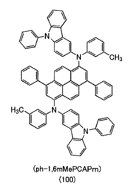

本実施例では、実施の形態1の構造式(101)で表される本発明の一態様である有機化合物、N,N’−ビス(9−フェニル−9H−カルバゾール−3−イル)−3,8−ジフェニル−N,N’−ジ(3,5−キシリル)−1,6−ピレンジアミン(略称:ph−1,6DMePCAPrn)の合成方法について説明する。なお、ph−1,6DMePCAPrnの構造式を以下に示す。


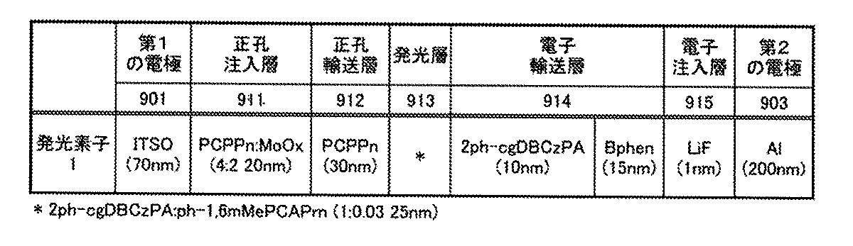

本実施例で示す発光素子は、図13に示すように基板900上に形成された第1の電極901上に発光層902として、正孔注入層911、正孔輸送層912、発光層913、電子輸送層914、電子注入層915が順次積層され、電子注入層915上に第2の電極903が積層された構造を有する。
作製した発光素子1の動作特性について測定した。なお、測定は室温で行った。また、発光素子1の動作特性の結果として電流密度−輝度特性を図14、電圧−輝度特性を図15、輝度−電流効率特性を図16、電圧−電流特性を図17にそれぞれ示す。


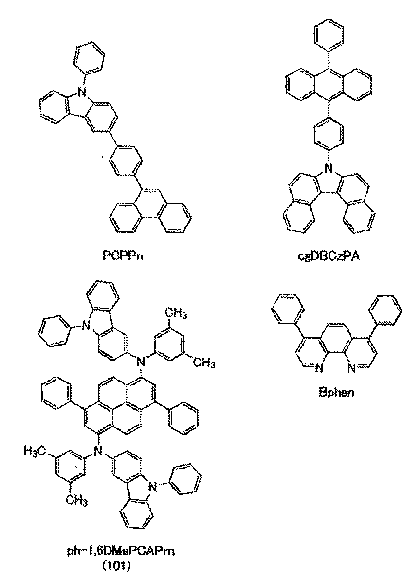
作製した発光素子2の動作特性について測定した。なお、測定は室温で行った。

Claims (12)
- 一般式(G1)で表される有機化合物。

- 一般式(G2)で表される有機化合物。
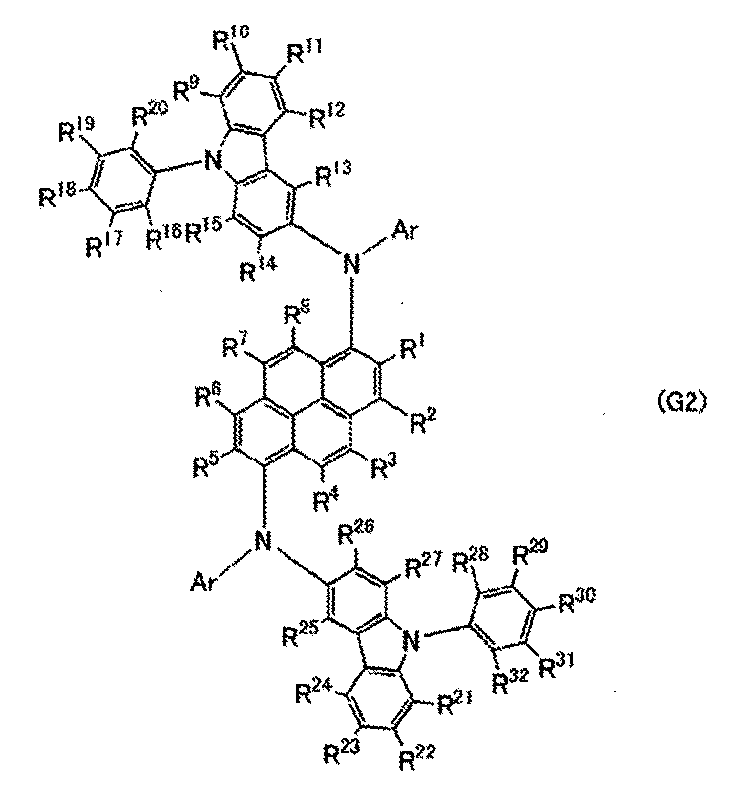
- 一般式(G3)で表される有機化合物。
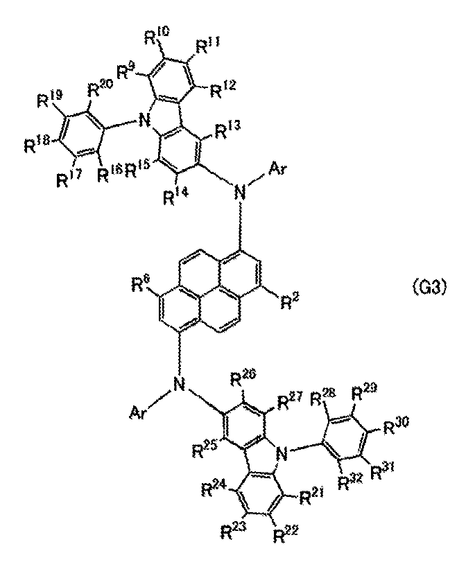
- 一般式(G4)で表される有機化合物。
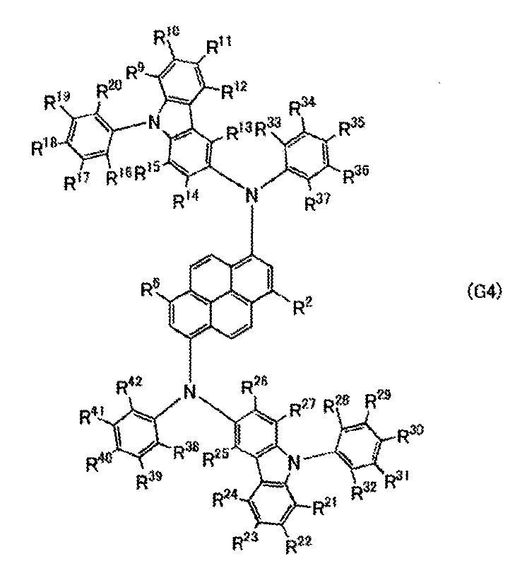
- 請求項1において、
R2およびR6は、下記構造式(Ar−1)乃至(Ar−7)のいずれか一で表されることを特徴とする有機化合物。
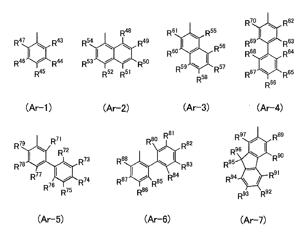
- 構造式(100)または構造式(101)で表される有機化合物。

- 請求項1乃至請求項6のいずれか一に記載の有機化合物を用いた発光素子。
- 一対の電極間にEL層を有し、
前記EL層は、請求項1乃至請求項6のいずれか一に記載の有機化合物を有する発光素子。 - 一対の電極間にEL層を有し、
前記EL層は、発光層を有し、
前記発光層は、請求項1乃至請求項6のいずれか一に記載の有機化合物を有する発光素子。 - 請求項7に記載の発光素子と、
トランジスタ、または基板の少なくとも一と、
を有する発光装置。 - 請求項10に記載の発光装置と、
マイク、カメラ、操作用ボタン、外部接続部、または、スピーカの少なくとも一と、
を有する電子機器。 - 請求項7に記載の発光素子と、
筐体、カバー、または、支持台の少なくとも一と、
を有する照明装置。
Priority Applications (3)
| Application Number | Priority Date | Filing Date | Title |
|---|---|---|---|
| CN201880046979.2A CN110891936A (zh) | 2017-07-14 | 2018-07-04 | 有机化合物、发光元件、发光装置、电子设备及照明装置 |
| KR1020207002381A KR102671111B1 (ko) | 2017-07-14 | 2018-07-04 | 유기 화합물, 발광 소자, 발광 장치, 전자 기기, 및 조명 장치 |
| JP2019529320A JP7225097B2 (ja) | 2017-07-14 | 2018-07-04 | 有機化合物、発光素子、発光装置、電子機器、および照明装置 |
Applications Claiming Priority (2)
| Application Number | Priority Date | Filing Date | Title |
|---|---|---|---|
| JP2017-137700 | 2017-07-14 | ||
| JP2017137700 | 2017-07-14 |
Publications (1)
| Publication Number | Publication Date |
|---|---|
| WO2019012373A1 true WO2019012373A1 (ja) | 2019-01-17 |
Family
ID=65001940
Family Applications (1)
| Application Number | Title | Priority Date | Filing Date |
|---|---|---|---|
| PCT/IB2018/054933 Ceased WO2019012373A1 (ja) | 2017-07-14 | 2018-07-04 | 有機化合物、発光素子、発光装置、電子機器、および照明装置 |
Country Status (4)
| Country | Link |
|---|---|
| JP (1) | JP7225097B2 (ja) |
| KR (1) | KR102671111B1 (ja) |
| CN (1) | CN110891936A (ja) |
| WO (1) | WO2019012373A1 (ja) |
Citations (12)
| Publication number | Priority date | Publication date | Assignee | Title |
|---|---|---|---|---|
| JP2005302667A (ja) * | 2004-04-15 | 2005-10-27 | Idemitsu Kosan Co Ltd | 有機エレクトロルミネッセンス素子 |
| WO2009107596A1 (ja) * | 2008-02-25 | 2009-09-03 | 出光興産株式会社 | 有機発光媒体及び有機el素子 |
| WO2010013676A1 (ja) * | 2008-07-28 | 2010-02-04 | 出光興産株式会社 | 有機発光媒体及び有機el素子 |
| WO2010013675A1 (ja) * | 2008-07-28 | 2010-02-04 | 出光興産株式会社 | 有機発光媒体及び有機el素子 |
| WO2010016405A1 (ja) * | 2008-08-07 | 2010-02-11 | 出光興産株式会社 | 新規芳香族アミン誘導体及びそれを用いた有機エレクトロルミネッセンス素子 |
| WO2010122810A1 (ja) * | 2009-04-24 | 2010-10-28 | 出光興産株式会社 | 芳香族アミン誘導体及びそれを用いた有機エレクトロルミネッセンス素子 |
| KR20110002155A (ko) * | 2009-07-01 | 2011-01-07 | 주식회사 엘지화학 | 신규한 화합물 및 이를 이용한 유기 전자 소자 |
| KR20110070180A (ko) * | 2009-12-18 | 2011-06-24 | 엘지디스플레이 주식회사 | 청색 형광 화합물 및 이를 이용한 유기전계 발광소자 |
| JP2013102146A (ja) * | 2011-10-11 | 2013-05-23 | Semiconductor Energy Lab Co Ltd | 発光素子、発光装置、電子機器、照明装置、およびピレン系化合物 |
| KR20140142923A (ko) * | 2013-06-05 | 2014-12-15 | 덕산하이메탈(주) | 광효율 개선층을 포함하는 유기전기소자 및 이를 포함하는 전자 장치 |
| WO2016072691A1 (ko) * | 2014-11-05 | 2016-05-12 | 덕산네오룩스 주식회사 | 유기전기소자용 조성물을 이용한 디스플레이 장치 및 유기전기소자 |
| KR20160059609A (ko) * | 2014-11-19 | 2016-05-27 | 덕산네오룩스 주식회사 | 유기전기소자용 조성물을 이용한 디스플레이 장치 및 유기전기소자 |
-
2018
- 2018-07-04 CN CN201880046979.2A patent/CN110891936A/zh active Pending
- 2018-07-04 KR KR1020207002381A patent/KR102671111B1/ko active Active
- 2018-07-04 JP JP2019529320A patent/JP7225097B2/ja active Active
- 2018-07-04 WO PCT/IB2018/054933 patent/WO2019012373A1/ja not_active Ceased
Patent Citations (12)
| Publication number | Priority date | Publication date | Assignee | Title |
|---|---|---|---|---|
| JP2005302667A (ja) * | 2004-04-15 | 2005-10-27 | Idemitsu Kosan Co Ltd | 有機エレクトロルミネッセンス素子 |
| WO2009107596A1 (ja) * | 2008-02-25 | 2009-09-03 | 出光興産株式会社 | 有機発光媒体及び有機el素子 |
| WO2010013676A1 (ja) * | 2008-07-28 | 2010-02-04 | 出光興産株式会社 | 有機発光媒体及び有機el素子 |
| WO2010013675A1 (ja) * | 2008-07-28 | 2010-02-04 | 出光興産株式会社 | 有機発光媒体及び有機el素子 |
| WO2010016405A1 (ja) * | 2008-08-07 | 2010-02-11 | 出光興産株式会社 | 新規芳香族アミン誘導体及びそれを用いた有機エレクトロルミネッセンス素子 |
| WO2010122810A1 (ja) * | 2009-04-24 | 2010-10-28 | 出光興産株式会社 | 芳香族アミン誘導体及びそれを用いた有機エレクトロルミネッセンス素子 |
| KR20110002155A (ko) * | 2009-07-01 | 2011-01-07 | 주식회사 엘지화학 | 신규한 화합물 및 이를 이용한 유기 전자 소자 |
| KR20110070180A (ko) * | 2009-12-18 | 2011-06-24 | 엘지디스플레이 주식회사 | 청색 형광 화합물 및 이를 이용한 유기전계 발광소자 |
| JP2013102146A (ja) * | 2011-10-11 | 2013-05-23 | Semiconductor Energy Lab Co Ltd | 発光素子、発光装置、電子機器、照明装置、およびピレン系化合物 |
| KR20140142923A (ko) * | 2013-06-05 | 2014-12-15 | 덕산하이메탈(주) | 광효율 개선층을 포함하는 유기전기소자 및 이를 포함하는 전자 장치 |
| WO2016072691A1 (ko) * | 2014-11-05 | 2016-05-12 | 덕산네오룩스 주식회사 | 유기전기소자용 조성물을 이용한 디스플레이 장치 및 유기전기소자 |
| KR20160059609A (ko) * | 2014-11-19 | 2016-05-27 | 덕산네오룩스 주식회사 | 유기전기소자용 조성물을 이용한 디스플레이 장치 및 유기전기소자 |
Also Published As
| Publication number | Publication date |
|---|---|
| CN110891936A (zh) | 2020-03-17 |
| JP7225097B2 (ja) | 2023-02-20 |
| JPWO2019012373A1 (ja) | 2020-07-30 |
| KR20200028401A (ko) | 2020-03-16 |
| KR102671111B1 (ko) | 2024-05-30 |
Similar Documents
| Publication | Publication Date | Title |
|---|---|---|
| JP7143310B2 (ja) | 有機化合物、発光素子、発光装置、電子機器、および照明装置 | |
| JP6487103B1 (ja) | 有機化合物、発光素子、発光装置、電子機器、および照明装置 | |
| JP7458452B2 (ja) | 発光素子 | |
| JP7297758B2 (ja) | 発光素子、発光装置、電子機器、および照明装置 | |
| JP2018100267A (ja) | 有機金属錯体、発光素子、発光装置、電子機器、および照明装置 | |
| WO2019229583A1 (ja) | 有機化合物、発光素子、発光装置、電子機器、および照明装置 | |
| JP2016197749A (ja) | 発光素子、発光装置、電子機器、照明装置及び薄膜太陽電池 | |
| WO2019229584A1 (ja) | 有機化合物、発光素子、発光装置、電子機器、および照明装置 | |
| JP2018065798A (ja) | 有機化合物、発光素子、発光装置、電子機器、および照明装置 | |
| JP2018052929A (ja) | 有機金属錯体、発光素子、発光装置、電子機器、および照明装置 | |
| JP2022166086A (ja) | 化合物 | |
| JP2019189540A (ja) | 有機化合物、発光素子、発光装置、電子機器、および照明装置 | |
| JP2023025011A (ja) | 発光素子 | |
| WO2020136496A1 (ja) | 有機化合物、発光デバイス、発光装置、電子機器、および照明装置 | |
| WO2018178818A1 (ja) | 有機化合物、発光素子、発光装置、電子機器、および照明装置 | |
| JP7225097B2 (ja) | 有機化合物、発光素子、発光装置、電子機器、および照明装置 | |
| JP7498113B2 (ja) | 有機化合物、発光デバイス、発光装置、電子機器、および照明装置 | |
| JP7287953B2 (ja) | 有機金属錯体、発光デバイス、発光装置、電子機器、および照明装置 | |
| WO2018189623A1 (ja) | 有機金属錯体、発光素子、発光装置、電子機器、および照明装置 | |
| JP2019142821A (ja) | 縮合カルバゾール骨格を有する有機化合物の合成方法 |
Legal Events
| Date | Code | Title | Description |
|---|---|---|---|
| 121 | Ep: the epo has been informed by wipo that ep was designated in this application |
Ref document number: 18831322 Country of ref document: EP Kind code of ref document: A1 |
|
| ENP | Entry into the national phase |
Ref document number: 2019529320 Country of ref document: JP Kind code of ref document: A |
|
| NENP | Non-entry into the national phase |
Ref country code: DE |
|
| ENP | Entry into the national phase |
Ref document number: 20207002381 Country of ref document: KR Kind code of ref document: A |
|
| 122 | Ep: pct application non-entry in european phase |
Ref document number: 18831322 Country of ref document: EP Kind code of ref document: A1 |