WO2019004486A2 - コード発生装置 - Google Patents
コード発生装置 Download PDFInfo
- Publication number
- WO2019004486A2 WO2019004486A2 PCT/JP2018/025120 JP2018025120W WO2019004486A2 WO 2019004486 A2 WO2019004486 A2 WO 2019004486A2 JP 2018025120 W JP2018025120 W JP 2018025120W WO 2019004486 A2 WO2019004486 A2 WO 2019004486A2
- Authority
- WO
- WIPO (PCT)
- Prior art keywords
- electrodes
- conductive
- panel
- electrode
- conductive pattern
- Prior art date
- Legal status (The legal status is an assumption and is not a legal conclusion. Google has not performed a legal analysis and makes no representation as to the accuracy of the status listed.)
- Ceased
Links
Images


Classifications
-
- G—PHYSICS
- G06—COMPUTING OR CALCULATING; COUNTING
- G06F—ELECTRIC DIGITAL DATA PROCESSING
- G06F3/00—Input arrangements for transferring data to be processed into a form capable of being handled by the computer; Output arrangements for transferring data from processing unit to output unit, e.g. interface arrangements
- G06F3/01—Input arrangements or combined input and output arrangements for interaction between user and computer
- G06F3/03—Arrangements for converting the position or the displacement of a member into a coded form
- G06F3/041—Digitisers, e.g. for touch screens or touch pads, characterised by the transducing means
- G06F3/044—Digitisers, e.g. for touch screens or touch pads, characterised by the transducing means by capacitive means
- G06F3/0447—Position sensing using the local deformation of sensor cells
-
- G—PHYSICS
- G06—COMPUTING OR CALCULATING; COUNTING
- G06F—ELECTRIC DIGITAL DATA PROCESSING
- G06F3/00—Input arrangements for transferring data to be processed into a form capable of being handled by the computer; Output arrangements for transferring data from processing unit to output unit, e.g. interface arrangements
- G06F3/01—Input arrangements or combined input and output arrangements for interaction between user and computer
- G06F3/03—Arrangements for converting the position or the displacement of a member into a coded form
- G06F3/033—Pointing devices displaced or positioned by the user, e.g. mice, trackballs, pens or joysticks; Accessories therefor
- G06F3/039—Accessories therefor, e.g. mouse pads
- G06F3/0393—Accessories for touch pads or touch screens, e.g. mechanical guides added to touch screens for drawing straight lines, hard keys overlaying touch screens or touch pads
-
- G—PHYSICS
- G06—COMPUTING OR CALCULATING; COUNTING
- G06F—ELECTRIC DIGITAL DATA PROCESSING
- G06F3/00—Input arrangements for transferring data to be processed into a form capable of being handled by the computer; Output arrangements for transferring data from processing unit to output unit, e.g. interface arrangements
- G06F3/01—Input arrangements or combined input and output arrangements for interaction between user and computer
- G06F3/03—Arrangements for converting the position or the displacement of a member into a coded form
- G06F3/041—Digitisers, e.g. for touch screens or touch pads, characterised by the transducing means
- G06F3/0412—Digitisers structurally integrated in a display
-
- G—PHYSICS
- G06—COMPUTING OR CALCULATING; COUNTING
- G06F—ELECTRIC DIGITAL DATA PROCESSING
- G06F3/00—Input arrangements for transferring data to be processed into a form capable of being handled by the computer; Output arrangements for transferring data from processing unit to output unit, e.g. interface arrangements
- G06F3/01—Input arrangements or combined input and output arrangements for interaction between user and computer
- G06F3/03—Arrangements for converting the position or the displacement of a member into a coded form
- G06F3/041—Digitisers, e.g. for touch screens or touch pads, characterised by the transducing means
- G06F3/0414—Digitisers, e.g. for touch screens or touch pads, characterised by the transducing means using force sensing means to determine a position
- G06F3/04146—Digitisers, e.g. for touch screens or touch pads, characterised by the transducing means using force sensing means to determine a position using pressure sensitive conductive elements delivering a boolean signal and located between crossing sensing lines, e.g. located between X and Y sensing line layers
-
- G—PHYSICS
- G06—COMPUTING OR CALCULATING; COUNTING
- G06F—ELECTRIC DIGITAL DATA PROCESSING
- G06F3/00—Input arrangements for transferring data to be processed into a form capable of being handled by the computer; Output arrangements for transferring data from processing unit to output unit, e.g. interface arrangements
- G06F3/01—Input arrangements or combined input and output arrangements for interaction between user and computer
- G06F3/03—Arrangements for converting the position or the displacement of a member into a coded form
- G06F3/041—Digitisers, e.g. for touch screens or touch pads, characterised by the transducing means
- G06F3/044—Digitisers, e.g. for touch screens or touch pads, characterised by the transducing means by capacitive means
- G06F3/0446—Digitisers, e.g. for touch screens or touch pads, characterised by the transducing means by capacitive means using a grid-like structure of electrodes in at least two directions, e.g. using row and column electrodes
Definitions
- the electrodes forming the respective conductive patterns are redundantly detected by the panel
- the number may be equal to or less than the number of multi-touches that the panel can simultaneously detect.
- the information processing apparatus connected to the panel is made to recognize the direction of the conductive pattern formed by detecting three or more electrodes uniquely disposed, and defined by the conductive pattern
- the capacitance code may be decoded.
- An information reading system includes a panel provided with a sensor that detects a change in physical quantity at one or more positions, an information processing apparatus that can be mounted on or externally connected to the panel, and a surface that contacts the panel. And the device according to any one of (1) to (52), wherein the panel detects one or more of the plurality of electrodes, and the information processing The device is characterized in that it decodes a capacitive code defined by the arrangement of said electrodes.
- the direction of the conductive pattern formed by detecting one or more electrodes is recognized, and the capacitance code defined by the conductive pattern is decoded, and the one conductive pattern is used as a reference pattern to carry out another conductive pattern. It recognizes the relative position of the electrode to form a pattern, to decode the capacitance code defined by the other conductive patterns, characterized in that.
- the panel Is formed by one or more electrodes disposed on the bottom of the device, and when subjected to a predetermined operation, at least a part of the conduction path between the electrodes and the conductive material is conducted or interrupted to Detecting a plurality of conductive patterns formed by the one or more electrodes detected in each of the plurality of electrodes, and an information processing apparatus connected to the panel detects at least one of the plurality of conductive
- the relative position of the electrodes forming the plurality of conductive patterns as a reference pattern for detecting the direction of the conductive pattern formed by detecting three or more electrodes arranged in and the arrangement of the other electrodes It recognized, decoding the plurality of electrostatic capacitance code defined by the conductive pattern of the plurality of, characterized in that.
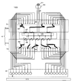
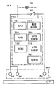
- the recognition unit recognizes the pattern code generated by the code generation unit of the code generation device 1 based on the detected conductive patterns of the one or more electrodes.
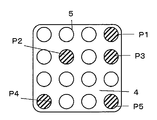
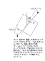
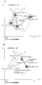
- the code recognition device 3 performs coordinate conversion by rotating the coordinate values on the touch panel by ⁇ ′. Coordinates after this coordinate conversion are called standardized coordinates, and coordinate values after the coordinate conversion are called standardized coordinate values.
- the coordinate value of each detection point is determined with P5 and P1 as the origin.
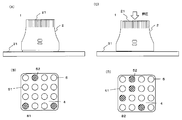
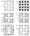
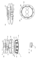
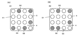
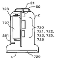
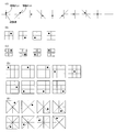
- the code generator 109 uses the first conductive pattern 81, the second conductive pattern 82, the third conductive pattern 83, and the fourth conductive pattern 84 as the setting unit 7 and supports them.
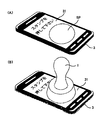
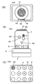
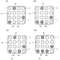
- the first conductive pattern is set to be changeable, and when placed on the touch panel 31, three sets of human-body contact conductive materials 21 and 211 are provided.
- , 212 can be selected to selectively generate the first, second, third, and fourth conductive patterns 81.82, 83, 84 by selecting, for example, a touch or no touch.
- the bonding method is not limited to double-sided tape, and bonding may be performed by applying an adhesive, as long as bonding can be performed to a degree that can be easily peeled off when peeling off the adhesive surface without causing positional deviation of the bonding surface.
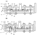
- the conductive pattern connection terminal 404 provided in the fold portion 403 of the conductive pattern printed sheet 400 can be crimped and conducted.
- the conductive adhesive or the conductive double-sided tape is placed between the connection terminals. Conduction between the connection terminals can be secured by coating or sticking.
- the connection resistance between the connection terminals may be lower than about several tens of K ⁇ .
- the number of the electrodes was 2 or less, the number of times when all the electrodes of the sample were detected in 10 trials was 50% or less, with or without the wiring. There was no specification which could detect all the electrodes ten times including rotation.
- a 12.5 mm wiring of 0.3 mm width can add a capacitance of 5.4 pF, and the detection performance can be slightly improved compared to no wiring.
- the capacitance per electrode is 2.6 pF on average, and there is variation among the electrodes (the slope of the graph is not uniform) because it also includes inter-electrode wiring capacitance.
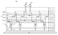
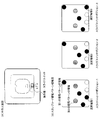
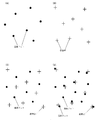
- FIG. 67 (F) to the second conductive pattern 82 of FIG.
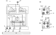
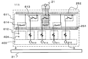
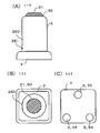
- the state of the second conductive pattern 82 of (F) is the case where the operation part 951 of the ID changeover switch 95 of the code generator 115 is aligned with the left contact among the three contacts (marks shown in FIG. The left side of the three electrodes 514 is detected by the touch panel at position “1” of 242, and the operation part 951 of the ID switch 95 is shown at the center contact position (FIG. 65A).
- the wiring it is preferable to shorten the wiring as much as possible because the largest error in the coordinates at which the electrode 5 is detected by the touch panel is the parasitic capacitance attached between the wiring of the portion corresponding to the bottom surface 4 of the conductive pattern printing sheet and the touch panel .
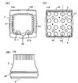
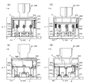
- the structure of the main body 207b including the lower housing 201a and the relative dielectric constant characteristics of the material have less influence on the electrode coordinates of the conductive pattern detected by the touch panel, the structure of the main body 207b and the ratio of the materials The restriction on the dielectric constant can be relaxed. Furthermore, since the flat plate 406 to which the conductive pattern printed sheet 400 is attached is fitted inside the step 230 of the lower housing 201a, the bonding position accuracy of the sheet and the lower housing is increased, and the ease of assembly is also improved. Do.
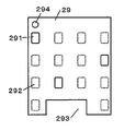
- FIGS. 92 to 94> The first example of the dot pattern is called by the applicant under a tentative name "GRID 0".
Landscapes
- Engineering & Computer Science (AREA)
- General Engineering & Computer Science (AREA)
- Theoretical Computer Science (AREA)
- Human Computer Interaction (AREA)
- Physics & Mathematics (AREA)
- General Physics & Mathematics (AREA)
- Switches That Are Operated By Magnetic Or Electric Fields (AREA)
- User Interface Of Digital Computer (AREA)
- Input From Keyboards Or The Like (AREA)
Priority Applications (9)
| Application Number | Priority Date | Filing Date | Title |
|---|---|---|---|
| US16/627,360 US20200387265A1 (en) | 2017-06-30 | 2018-07-02 | Code generation device |
| EP18823310.0A EP3647916A4 (en) | 2017-06-30 | 2018-07-02 | CODE GENERATION DEVICE |
| JP2019527101A JPWO2019004486A1 (ja) | 2017-06-30 | 2018-07-02 | コード発生装置 |
| JP2019000364A JP6613407B2 (ja) | 2017-12-29 | 2019-01-04 | コード発生装置 |
| JP2019021977A JP6610916B2 (ja) | 2017-12-29 | 2019-02-08 | コード発生装置 |
| US17/257,624 US20220058355A1 (en) | 2017-12-29 | 2019-07-02 | Code generation device |
| PCT/JP2019/026392 WO2020009131A1 (ja) | 2017-12-29 | 2019-07-02 | コード発生装置 |
| JP2020529018A JPWO2020009131A1 (ja) | 2017-06-30 | 2019-07-02 | コード発生装置 |
| JP2019188323A JP2020021507A (ja) | 2017-12-29 | 2019-10-15 | コード発生装置 |
Applications Claiming Priority (4)
| Application Number | Priority Date | Filing Date | Title |
|---|---|---|---|
| JP2017129968 | 2017-06-30 | ||
| JP2017-129968 | 2017-06-30 | ||
| JP2017-255255 | 2017-12-29 | ||
| JP2017255255 | 2017-12-29 |
Publications (2)
| Publication Number | Publication Date |
|---|---|
| WO2019004486A2 true WO2019004486A2 (ja) | 2019-01-03 |
| WO2019004486A3 WO2019004486A3 (ja) | 2019-03-28 |
Family
ID=64480456
Family Applications (1)
| Application Number | Title | Priority Date | Filing Date |
|---|---|---|---|
| PCT/JP2018/025120 Ceased WO2019004486A2 (ja) | 2017-06-30 | 2018-07-02 | コード発生装置 |
Country Status (4)
| Country | Link |
|---|---|
| US (1) | US20200387265A1 (https=) |
| EP (1) | EP3647916A4 (https=) |
| JP (4) | JP6427745B1 (https=) |
| WO (1) | WO2019004486A2 (https=) |
Cited By (1)
| Publication number | Priority date | Publication date | Assignee | Title |
|---|---|---|---|---|
| JPWO2020009131A1 (ja) * | 2017-06-30 | 2021-09-30 | 株式会社I・Pソリューションズ | コード発生装置 |
Families Citing this family (6)
| Publication number | Priority date | Publication date | Assignee | Title |
|---|---|---|---|---|
| US11539511B2 (en) * | 2019-08-08 | 2022-12-27 | Lenovo (Singapore) Pte. Ltd. | Use of conductive ink segments to establish secure device key |
| WO2021079432A1 (ja) * | 2019-10-23 | 2021-04-29 | 三菱電機株式会社 | 操作支援装置、タッチパネル入力システム、操作判定方法、及びプログラム |
| US11182038B2 (en) * | 2020-04-08 | 2021-11-23 | Sigmasense, Llc. | Encoded data pattern touchscreen sensing system |
| JP2022035357A (ja) * | 2020-08-20 | 2022-03-04 | 株式会社空環工房 | コンテンツ提供装置、コンテンツ提供システム、コンテンツ提供プログラムおよびコンテンツ提供方法 |
| KR20230118720A (ko) * | 2022-02-04 | 2023-08-14 | 삼성디스플레이 주식회사 | 표시 장치 및 이를 포함하는 터치 입력 시스템 |
| JP2025040768A (ja) * | 2023-09-12 | 2025-03-25 | 株式会社ベネッセコーポレーション | 入力デバイス、情報処理システム、情報処理方法及び情報処理プログラム |
Citations (2)
| Publication number | Priority date | Publication date | Assignee | Title |
|---|---|---|---|---|
| JP2015005275A (ja) | 2013-05-22 | 2015-01-08 | 株式会社Leonis&Co. | 電子チケットシステムおよびプログラム |
| JP2016505922A (ja) | 2012-11-19 | 2016-02-25 | 12シイエム | スタンプタッチ認証方法及びシステム |
Family Cites Families (10)
| Publication number | Priority date | Publication date | Assignee | Title |
|---|---|---|---|---|
| MX2013008668A (es) * | 2011-06-22 | 2014-04-30 | Ibm | Dispositivo de generacion tactil para aparatos moviles y comunicacion con pantalla tactil. |
| KR101305412B1 (ko) * | 2012-01-09 | 2013-09-06 | 최영우 | 터치스크린이 채용된 휴대 단말기용 터치스탬프 및 이를 이용한 인증시스템 및 방법 |
| JP2015075796A (ja) * | 2013-10-06 | 2015-04-20 | 信行 千葉 | 入力デバイス |
| JP2015138361A (ja) * | 2014-01-22 | 2015-07-30 | 株式会社エヌディエス | タッチパネルの検知面への接触装置 |
| EP3296844A4 (en) * | 2015-05-13 | 2018-12-26 | playground Co., Ltd. | Terminal device, electronic stamp, and program |
| JP6031689B1 (ja) * | 2015-09-21 | 2016-11-24 | 株式会社I・Pソリューションズ | 装置、及びカード型装置 |
| JP5911995B1 (ja) * | 2015-09-21 | 2016-04-27 | 株式会社I・Pソリューションズ | 装置、情報処理装置、プログラムおよび情報処理システム |
| JP2018045509A (ja) * | 2016-09-15 | 2018-03-22 | 富士通株式会社 | 端末装置、特殊操作制御方法および特殊操作制御プログラム |
| US20200387265A1 (en) * | 2017-06-30 | 2020-12-10 | I.P Solutions, Ltd. | Code generation device |
| JP6613407B2 (ja) * | 2017-12-29 | 2019-12-04 | 株式会社I・Pソリューションズ | コード発生装置 |
-
2018
- 2018-07-02 US US16/627,360 patent/US20200387265A1/en not_active Abandoned
- 2018-07-02 JP JP2018126428A patent/JP6427745B1/ja active Active
- 2018-07-02 WO PCT/JP2018/025120 patent/WO2019004486A2/ja not_active Ceased
- 2018-07-02 JP JP2019527101A patent/JPWO2019004486A1/ja active Pending
- 2018-07-02 EP EP18823310.0A patent/EP3647916A4/en not_active Withdrawn
- 2018-09-19 JP JP2018175260A patent/JP2019109878A/ja active Pending
-
2019
- 2019-07-02 JP JP2020529018A patent/JPWO2020009131A1/ja active Pending
Patent Citations (2)
| Publication number | Priority date | Publication date | Assignee | Title |
|---|---|---|---|---|
| JP2016505922A (ja) | 2012-11-19 | 2016-02-25 | 12シイエム | スタンプタッチ認証方法及びシステム |
| JP2015005275A (ja) | 2013-05-22 | 2015-01-08 | 株式会社Leonis&Co. | 電子チケットシステムおよびプログラム |
Non-Patent Citations (1)
| Title |
|---|
| See also references of EP3647916A4 |
Cited By (1)
| Publication number | Priority date | Publication date | Assignee | Title |
|---|---|---|---|---|
| JPWO2020009131A1 (ja) * | 2017-06-30 | 2021-09-30 | 株式会社I・Pソリューションズ | コード発生装置 |
Also Published As
| Publication number | Publication date |
|---|---|
| JPWO2020009131A1 (ja) | 2021-09-30 |
| EP3647916A4 (en) | 2021-03-31 |
| WO2019004486A3 (ja) | 2019-03-28 |
| US20200387265A1 (en) | 2020-12-10 |
| EP3647916A2 (en) | 2020-05-06 |
| JP6427745B1 (ja) | 2018-11-28 |
| JP2019109878A (ja) | 2019-07-04 |
| JPWO2019004486A1 (ja) | 2020-08-27 |
| JP2019109873A (ja) | 2019-07-04 |
Similar Documents
| Publication | Publication Date | Title |
|---|---|---|
| JP6613407B2 (ja) | コード発生装置 | |
| JP6427745B1 (ja) | コード発生装置 | |
| US10643046B2 (en) | Device, and card type device | |
| EP3355168A1 (en) | Device, and card type device | |
| US20140284382A1 (en) | Random-type multilayer identification, and system using same | |
| KR102168577B1 (ko) | 장치 및 카드형 장치 | |
| US10884564B2 (en) | Sheet-shaped device | |
| CN106168875A (zh) | 移动终端及其控制方法 | |
| CN203720859U (zh) | 具有指纹识别功能的触控盖板及电子设备 | |
| NZ539291A (en) | Identification system | |
| JPWO2017142093A1 (ja) | 装置、及びカード型装置 | |
| CN207926668U (zh) | 显示屏组件,透明盖板和电子设备 | |
| CN203930880U (zh) | 指纹识别检测组件及其电子装置 | |
| KR101060060B1 (ko) | 랜덤형 다층 인식체를 이용한 인증시스템 | |
| KR20150134109A (ko) | 터치 인식을 이용한 역방향 가치 사용 방법 | |
| CN107239719A (zh) | 特征数据生成装置、读卡器,数据处理系统及方法 | |
| KR20130037905A (ko) | 다층인식체용 인식장치 | |
| JP2018041232A (ja) | 入力デバイスおよび情報処理装置 | |
| KR20150134064A (ko) | 동시 터치 기반 서비스 제공 방법 |
Legal Events
| Date | Code | Title | Description |
|---|---|---|---|
| 121 | Ep: the epo has been informed by wipo that ep was designated in this application |
Ref document number: 18823310 Country of ref document: EP Kind code of ref document: A2 |
|
| NENP | Non-entry into the national phase |
Ref country code: DE |
|
| ENP | Entry into the national phase |
Ref document number: 2018823310 Country of ref document: EP Effective date: 20200130 |
|
| ENP | Entry into the national phase |
Ref document number: 2019527101 Country of ref document: JP Kind code of ref document: A |