WO2018235590A1 - Wiring board production method and conductive ink - Google Patents
Wiring board production method and conductive ink Download PDFInfo
- Publication number
- WO2018235590A1 WO2018235590A1 PCT/JP2018/021514 JP2018021514W WO2018235590A1 WO 2018235590 A1 WO2018235590 A1 WO 2018235590A1 JP 2018021514 W JP2018021514 W JP 2018021514W WO 2018235590 A1 WO2018235590 A1 WO 2018235590A1
- Authority
- WO
- WIPO (PCT)
- Prior art keywords
- conductive ink
- transfer film
- substrate
- wiring
- layer
- Prior art date
Links
Images


Classifications
-
- H—ELECTRICITY
- H05—ELECTRIC TECHNIQUES NOT OTHERWISE PROVIDED FOR
- H05K—PRINTED CIRCUITS; CASINGS OR CONSTRUCTIONAL DETAILS OF ELECTRIC APPARATUS; MANUFACTURE OF ASSEMBLAGES OF ELECTRICAL COMPONENTS
- H05K3/00—Apparatus or processes for manufacturing printed circuits
- H05K3/10—Apparatus or processes for manufacturing printed circuits in which conductive material is applied to the insulating support in such a manner as to form the desired conductive pattern
- H05K3/20—Apparatus or processes for manufacturing printed circuits in which conductive material is applied to the insulating support in such a manner as to form the desired conductive pattern by affixing prefabricated conductor pattern
- H05K3/207—Apparatus or processes for manufacturing printed circuits in which conductive material is applied to the insulating support in such a manner as to form the desired conductive pattern by affixing prefabricated conductor pattern using a prefabricated paste pattern, ink pattern or powder pattern
-
- C—CHEMISTRY; METALLURGY
- C09—DYES; PAINTS; POLISHES; NATURAL RESINS; ADHESIVES; COMPOSITIONS NOT OTHERWISE PROVIDED FOR; APPLICATIONS OF MATERIALS NOT OTHERWISE PROVIDED FOR
- C09D—COATING COMPOSITIONS, e.g. PAINTS, VARNISHES OR LACQUERS; FILLING PASTES; CHEMICAL PAINT OR INK REMOVERS; INKS; CORRECTING FLUIDS; WOODSTAINS; PASTES OR SOLIDS FOR COLOURING OR PRINTING; USE OF MATERIALS THEREFOR
- C09D11/00—Inks
- C09D11/30—Inkjet printing inks
- C09D11/38—Inkjet printing inks characterised by non-macromolecular additives other than solvents, pigments or dyes
-
- C—CHEMISTRY; METALLURGY
- C09—DYES; PAINTS; POLISHES; NATURAL RESINS; ADHESIVES; COMPOSITIONS NOT OTHERWISE PROVIDED FOR; APPLICATIONS OF MATERIALS NOT OTHERWISE PROVIDED FOR
- C09D—COATING COMPOSITIONS, e.g. PAINTS, VARNISHES OR LACQUERS; FILLING PASTES; CHEMICAL PAINT OR INK REMOVERS; INKS; CORRECTING FLUIDS; WOODSTAINS; PASTES OR SOLIDS FOR COLOURING OR PRINTING; USE OF MATERIALS THEREFOR
- C09D11/00—Inks
- C09D11/52—Electrically conductive inks
-
- H—ELECTRICITY
- H01—ELECTRIC ELEMENTS
- H01B—CABLES; CONDUCTORS; INSULATORS; SELECTION OF MATERIALS FOR THEIR CONDUCTIVE, INSULATING OR DIELECTRIC PROPERTIES
- H01B13/00—Apparatus or processes specially adapted for manufacturing conductors or cables
-
- H—ELECTRICITY
- H05—ELECTRIC TECHNIQUES NOT OTHERWISE PROVIDED FOR
- H05K—PRINTED CIRCUITS; CASINGS OR CONSTRUCTIONAL DETAILS OF ELECTRIC APPARATUS; MANUFACTURE OF ASSEMBLAGES OF ELECTRICAL COMPONENTS
- H05K1/00—Printed circuits
- H05K1/02—Details
- H05K1/09—Use of materials for the conductive, e.g. metallic pattern
- H05K1/092—Dispersed materials, e.g. conductive pastes or inks
- H05K1/097—Inks comprising nanoparticles and specially adapted for being sintered at low temperature
-
- H—ELECTRICITY
- H05—ELECTRIC TECHNIQUES NOT OTHERWISE PROVIDED FOR
- H05K—PRINTED CIRCUITS; CASINGS OR CONSTRUCTIONAL DETAILS OF ELECTRIC APPARATUS; MANUFACTURE OF ASSEMBLAGES OF ELECTRICAL COMPONENTS
- H05K3/00—Apparatus or processes for manufacturing printed circuits
- H05K3/10—Apparatus or processes for manufacturing printed circuits in which conductive material is applied to the insulating support in such a manner as to form the desired conductive pattern
- H05K3/12—Apparatus or processes for manufacturing printed circuits in which conductive material is applied to the insulating support in such a manner as to form the desired conductive pattern using thick film techniques, e.g. printing techniques to apply the conductive material or similar techniques for applying conductive paste or ink patterns
- H05K3/1241—Apparatus or processes for manufacturing printed circuits in which conductive material is applied to the insulating support in such a manner as to form the desired conductive pattern using thick film techniques, e.g. printing techniques to apply the conductive material or similar techniques for applying conductive paste or ink patterns by ink-jet printing or drawing by dispensing
- H05K3/125—Apparatus or processes for manufacturing printed circuits in which conductive material is applied to the insulating support in such a manner as to form the desired conductive pattern using thick film techniques, e.g. printing techniques to apply the conductive material or similar techniques for applying conductive paste or ink patterns by ink-jet printing or drawing by dispensing by ink-jet printing
-
- H—ELECTRICITY
- H05—ELECTRIC TECHNIQUES NOT OTHERWISE PROVIDED FOR
- H05K—PRINTED CIRCUITS; CASINGS OR CONSTRUCTIONAL DETAILS OF ELECTRIC APPARATUS; MANUFACTURE OF ASSEMBLAGES OF ELECTRICAL COMPONENTS
- H05K2201/00—Indexing scheme relating to printed circuits covered by H05K1/00
- H05K2201/01—Dielectrics
- H05K2201/0137—Materials
- H05K2201/0145—Polyester, e.g. polyethylene terephthalate [PET], polyethylene naphthalate [PEN]
-
- H—ELECTRICITY
- H05—ELECTRIC TECHNIQUES NOT OTHERWISE PROVIDED FOR
- H05K—PRINTED CIRCUITS; CASINGS OR CONSTRUCTIONAL DETAILS OF ELECTRIC APPARATUS; MANUFACTURE OF ASSEMBLAGES OF ELECTRICAL COMPONENTS
- H05K2201/00—Indexing scheme relating to printed circuits covered by H05K1/00
- H05K2201/02—Fillers; Particles; Fibers; Reinforcement materials
- H05K2201/0203—Fillers and particles
- H05K2201/0242—Shape of an individual particle
- H05K2201/026—Nanotubes or nanowires
-
- H—ELECTRICITY
- H05—ELECTRIC TECHNIQUES NOT OTHERWISE PROVIDED FOR
- H05K—PRINTED CIRCUITS; CASINGS OR CONSTRUCTIONAL DETAILS OF ELECTRIC APPARATUS; MANUFACTURE OF ASSEMBLAGES OF ELECTRICAL COMPONENTS
- H05K2203/00—Indexing scheme relating to apparatus or processes for manufacturing printed circuits covered by H05K3/00
- H05K2203/01—Tools for processing; Objects used during processing
- H05K2203/0147—Carriers and holders
- H05K2203/0156—Temporary polymeric carrier or foil, e.g. for processing or transferring
-
- H—ELECTRICITY
- H05—ELECTRIC TECHNIQUES NOT OTHERWISE PROVIDED FOR
- H05K—PRINTED CIRCUITS; CASINGS OR CONSTRUCTIONAL DETAILS OF ELECTRIC APPARATUS; MANUFACTURE OF ASSEMBLAGES OF ELECTRICAL COMPONENTS
- H05K2203/00—Indexing scheme relating to apparatus or processes for manufacturing printed circuits covered by H05K3/00
- H05K2203/11—Treatments characterised by their effect, e.g. heating, cooling, roughening
- H05K2203/1131—Sintering, i.e. fusing of metal particles to achieve or improve electrical conductivity
Definitions
- the present invention relates to a method of manufacturing a wiring substrate and a conductive ink.
- a wiring board in which a wiring pattern is formed on a substrate is known.
- a method of forming such a wiring pattern a method of forming a wiring pattern by etching a metal layer provided on a substrate, a method of forming a wiring pattern using a conductive paste or a conductive ink, and And a method of forming a wiring pattern by electroless plating.
- Patent Document 1 shows a method of manufacturing a wiring pattern using a conductive ink (a method of manufacturing a wiring substrate). Specifically, after peeling the support film from the transfer film on which the support film, the adhesive layer, the conductive layer (wiring pattern) obtained using the conductive ink, and the protective layer are laminated in this order, the adhesive layer is removed. A method of bonding the conductive layer on the substrate via the substrate is disclosed (claims 1, 4 and the like).
- the inventor used a conductive ink from the side opposite to the support for a specific transfer film in which the support, the protective layer, and the receiving layer were laminated in this order. It has been found that printing can be performed and wiring boards can be easily manufactured using the obtained transfer film, and the present invention has been achieved. That is, the present inventor has found that the above problem can be solved by the following configuration.
- a support A protective layer formed on one surface of the support and releasable from the support; A receiving layer formed on the surface of the protective layer and receiving the solvent in a conductive ink containing a conductive substance and a solvent;
- a method of manufacturing a wiring board comprising: [2] The method for producing a wiring board according to [1], wherein the transfer film further has a solvent permeation layer formed on the surface of the receiving layer and having a void
- [3] The method for producing a wiring board according to [1] or [2], wherein the printing is performed by an inkjet method.
- [4] The method for producing a wiring board according to any one of [1] to [3], wherein the sticking step is performed under heating.
- [5] The manufacturing method of the wiring board as described in [4] whose heating temperature in the said adhesion
- [6] A procedure of peeling a support in the new transfer film after sticking a new transfer film on which the wiring pattern obtained in the wiring pattern formation step is formed on the wiring substrate obtained in the peeling step The method of manufacturing a wiring board according to any one of [1] to [5], wherein a plurality of wiring patterns are stacked on the substrate.
- the conductive material is a metal nanowire having an aspect ratio of 200 or more
- the manufacturing method of the wiring board as described in [9] whose mass ratio of the said metal nanowire with respect to the compound represented by the said Formula (I) is more than 10 and less than 1000.
- a conductive ink comprising a solvent, a compound represented by Formula (I) described later, and a metal nanowire having an aspect ratio of 200 or more.
- X represents a gold atom, a palladium atom or a platinum atom.
- X represents a gold atom, a palladium atom or a platinum atom.
- a method of manufacturing a wiring board capable of easily manufacturing a wiring board protected by an insulating layer, and a conductive ink.
- a method of manufacturing a wiring substrate which does not require processes such as development, etching and baking.
- the present invention will be described below. Although the description of the configuration requirements described below may be made based on the representative embodiments of the present invention, the present invention is not limited to such embodiments.
- the numerical range represented using “to” in the present invention means a range including the numerical values described before and after “to” as the lower limit value and the upper limit value.
- (meth) acrylic means a generic name of "acrylic” and "methacrylic”.
- the method for producing a wiring substrate of the present invention comprises a support, a protective layer formed on one surface of the support and removable from the support, and the protective layer.
- Production of a wiring substrate using a transfer film (hereinafter, also referred to as "specific transfer film") having a receptor layer formed on the surface of the conductive ink and containing the above-mentioned solvent in the conductive ink containing the conductive substance and the solvent. It is a method.
- a wiring pattern is formed on the specific transfer film by printing using the conductive ink from the surface of the transfer film opposite to the surface on which the support is formed.
- the step of forming the wiring pattern After the step of forming the wiring pattern, the surface opposite to the surface on which the support is formed of the specific transfer film on which the wiring pattern is formed is brought into contact with the substrate to attach the specific transfer film and the substrate The sticking process to wear, After the sticking step, the step of peeling the support from the specific transfer film stuck to the substrate to obtain a wiring board is provided.
- the process of forming the protective layer since printing is performed on the specific transfer film on which the protective layer is formed in advance, the process of forming the protective layer is not necessary between the wiring pattern forming process and the adhering process, and the process from printing to adhering Can be implemented smoothly.
- the wiring substrate can be manufactured by a simple process.
- the wiring can be directly stuck to the surface which can not be developed, etched and fired, for example, the apparatus.
- the material used by this manufacturing method is explained in full detail first, and, after that, each process is explained in full detail.
- the specific transfer film used in this production method is formed on a support, a protective layer formed on one surface of the support and removable from the support, and a surface of the protective layer, and a conductive substance and a solvent. And a receptive layer for receiving the solvent in the conductive ink.
- the specific transfer film may have a solvent permeable layer formed on the surface of the receptive layer and having a void through which the solvent in the conductive ink can penetrate.
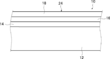
- FIG. 1 is a cross-sectional view schematically showing an example of the specific transfer film.
- the transfer film 10 comprises a support 12, a protective layer 14 formed on one surface of the support 12, a receptive layer 16 formed on the surface of the protective layer 14, and a receptive layer 16 And a solvent permeation layer 18 formed on the surface of
- the solvent permeation layer 18 is adhered to the substrate P, and then the support 12 is a protective layer
- the laminate including the solvent permeation layer 18, the receiving layer 16 and the protective layer 14 is transferred to the substrate P, and a wiring pattern is formed on the substrate P. Therefore, in a state in which the laminate including the solvent permeation layer 18, the receiving layer 16 and the protective layer 14 is transferred to the substrate P, the protective layer 14 becomes the surface and the solvent permeation layer 18 becomes the substrate P side.
- the support 12 supports the protective layer 14, the receptive layer 16 and the solvent permeation layer 18 until the transfer film 10 is adhered to the substrate P.
- the support 12 various known sheet materials (films) capable of supporting the protective layer 14, the receptive layer 16 and the solvent permeation layer 18 can be used.
- the sticking step described later is carried out under heating (that is, in the case of heat sticking)
- the support 12 having sufficient heat resistance.
- Specific examples of the support 12 include resin films formed of various resin materials.
- Specific examples of the resin material to be the support 12 include polyester resins such as polyethylene terephthalate (PET (polyethylene terephthalate)) and polyethylene naphthalate (PEN (polyethylene naphthalate)), polycarbonate resins, acrylic resins, methacrylic resins, and And polyimide resins.
- the thickness of the support 12 is not particularly limited, but the protective layer 14, the receptive layer 16 and the solvent permeation layer 18 can be supported until the adhesion process described later is performed, and the transfer film 10 is adhered to the substrate P After that, a thickness that can be properly peeled without causing breakage or the like may be appropriately set according to the forming material or the like.
- the thickness of the support 12 is preferably 20 to 200 ⁇ m, and more preferably 50 to 130 ⁇ m.
- Protective layer 14 is formed on one surface of support 12.
- the protective layer 14 is a layer that protects the receptive layer 16 after the peeling process described later.
- the protective layer 14 preferably comprises a polymer. 0 degreeC or more is preferable, as for the glass transition temperature (Tg) of the polymer which may be contained in the protective layer 14, 20 degreeC or more is more preferable, and 30 degreeC or more is more preferable.
- Tg glass transition temperature
- the upper limit of the Tg of the polymer that can be contained in the protective layer 14 is preferably 80 ° C. or less. If the Tg of the above-mentioned polymer is 80 ° C.
- the protective layer 14 can be favorably formed (film-formed), and since the film-forming temperature can be lowered, the selection range of the support 12 can be expanded.
- the Tg of the polymer may be measured by a known method, or the numerical values described in various documents may be used, and when using a commercially available polymer, the numerical values described in the catalog etc. Or a numerical value calculated from the composition of the polymer.
- the measuring method of glass transition temperature the method of measuring based on JIS (Japanese Industrial Standards) K7121 by a differential scanning calorimetry is mentioned.
- the solubility parameter (SP value) of the polymer that can be contained in the protective layer 14 is preferably 8.5 (cal / cm 3 ) 1/2 or more, and more preferably 9.0 (cal / cm 3 ) 1/2 or more.
- the protective layer 14 can be formed of a polymer having high polarity and strong molecular cohesion, so that the scratch resistance of the protective layer 14 becomes good.
- there are advantages such as high tensile strength of the protective layer 14 and good peelability.
- the solubility parameter of the polymer may be measured by a known method, or the numerical values described in various documents may be used, and in the case of using a commercially available polymer, it is described in a catalog etc. You may use a numerical value.
- the formation of the wiring pattern on the substrate P using the transfer film 10 is carried out by adhering the solvent permeation layer 18 and the substrate P in a state where the solvent permeation layer 18 and the substrate P are in contact with each other as described above , By peeling the support 12.
- the lower limit of the thickness of the protective layer 14 is not particularly limited, and a thickness that can sufficiently protect the receiving layer 16 may be appropriately set according to the material of the protective layer 14.
- the thickness of the protective layer 14 is preferably 1 ⁇ m or more, and more preferably 2 ⁇ m or more.
- the protective layer 14 may have a single-layer structure or a multi-layer structure.
- polymers that can be included in the protective layer 14 various known polymers can be used.
- urethane based polymer acrylic based polymer, vinyl acetate based polymer, polyvinyl chloride based polymer, rubber based polymer, styrene based polymer, silicone based polymer, ester based polymer, amide based polymer, and repeating units constituting these polymers
- the copolymer which contains multiple types is mentioned.
- urethane polymers are preferable in that the releasability of the support 12 is more excellent.
- the polymer which may be contained in the protective layer 14 may use a commercial item.
- specific examples of the polymer having a Tg of 0 ° C. or higher include Superflex 170 (urethane-based polymer), Superflex 820 (urethane-based polymer), Superflex 830HS (urethane-based polymer) manufactured by Daiichi Kogyo Seiyaku Co., Ltd.
- the protective layer 14 may contain two or more types of polymers, and it is preferable that the Tg of each of the two or more types of polymers is 0 ° C. or more.
- the protective layer 14 contains 2 or more types of polymers, the characteristic of each polymer is expressed, and the transfer film 10 which is excellent in transferability and the flaw resistance of a protective layer is obtained.
- a urethane polymer and an ethylene-vinyl acetate-vinyl chloride copolymer are used in combination, a transfer film 10 excellent in the peelability of the support 12 and the scratch resistance of the protective layer 14 can be obtained.
- the content of the polymer having a Tg of 0 ° C. or more is preferably 20% by mass or more, more preferably 30% by mass or more, and still more preferably 50% by mass or more based on the total mass of the protective layer 14. If the content of the polymer having a Tg of 0 ° C. or more is 20% by mass or more, the releasability between the support 12 and the protective layer 14 becomes good, the scratch resistance of the protective layer 14 becomes good, It is preferable from the point that bendability (flexibility) becomes good.
- the protective layer 14 may contain a surfactant. If the protective layer 14 contains a surfactant, the releasability between the support 12 and the protective layer 14 can be improved.
- the surfactant can use the well-known surfactant according to the formation material of the protective layer 14. Specific examples of the surfactant include ethers such as polyoxyethylene nonyl phenyl ether, polyoxyethylene octyl phenyl ether, polyoxyethylene dodecyl phenyl ether, polyoxyethylene oleyl ether, polyoxyethylene lauryl ether, polyoxyethylene alkyl ether, etc.
- Emulgen series such as Kao Corp.'s Emulgen 108, 109 P, etc., Nippon Tanso Co., Ltd. Softanol EP-5035, 7085, 9050, Adeka's Pluronic L-31, L-34, L-44 etc.
- Esters such as polyoxyethylene oleate, polyoxyethylene distearate, sorbitan laurate, sorbitan monostearate, sorbitan monooleate, sorbitan sesquioleate, polyoxyethylene monooleate, polyoxyethylene stearate and the like; Polyoxyethylene acetylene glycol ether, polyoxyethylene distyrenated phenyl ether, polyoxyethylene tribenzylated phenyl ether, etc.
- Nonionic surfactants such as 485, olfine STG, etc .; polyglycol ethers; etc. may be mentioned.
- the content of the surfactant is preferably 0.01 to 5% by mass, and more preferably 0.1 to 2% by mass, with respect to the total mass of the protective layer 14.
- the protective layer 14 may contain components other than the above as required, and examples thereof include various additives such as waxes, inorganic pigments, ultraviolet absorbers, and antioxidants.
- the receptive layer 16 is formed on the surface of the protective layer 14.
- the receiving layer 16 is a layer that receives a solvent (water and / or an organic solvent) contained in the conductive ink. Specifically, the receptive layer 16 penetrates the solvent permeation layer 18 and mainly accepts the solvent contained in the conductive ink that has passed through the solvent permeation layer 18.
- the receptive layer 16 is not limited to the solvent contained in the conductive ink, but may be a component (a liquid or a solid which has passed through the solvent permeation layer 18). For example, conductive materials and coloring materials may be mentioned. Can be accepted.
- the receiving layer 16 is a layer formed using a polymer that receives and swells a solvent, or voids (fine particles) in which fine particles insoluble in the solvent (dispersion medium) contained in the conductive ink are fixed by the binder. Layers having holes).
- the transfer film 10 has the solvent permeable layer 18
- a conductive substance and necessary Accordingly, the color material etc. used is held.
- FIG. 2 conceptually shows an example of the configuration of the receiving layer 16.
- the receiving layer 16 shown in FIG. 2 is formed by fixing a plurality of receiving particles 20 insoluble in the conductive ink with a binder, and the ink is received in each gap of the receiving particles 20.
- the conductive ink contains a coloring material (described later)
- a fixing agent for fixing the coloring material in the conductive ink between the receiving particles 20 and a material that does not cause aggregation For example, nonpolar or low polar materials are used.
- the receptor particles 20 include polymer fine particles such as polyolefin, acrylic, polystyrene, and polyester, and inorganic substances such as calcium carbonate, kaolin, aluminum silicate, calcium silicate, colloidal silica, alumina, and aluminum hydroxide. There are fine particles.
- the binder for fixing the receiving particle 20 include water-soluble polymers such as gelatin, polyvinyl alcohol, polyvinyl pyrrolidone, alginic acid, aqueous polyester, and aqueous acrylic resin. Where the conductive ink comprises metal nanowires, polyvinyl pyrrolidone is preferred, which can also be stabilized with aqueous and solvent inks.
- the colorant may be received by the receiving layer 16.
- the receptive layer 16 itself has a light scattering ability, the light is scattered when the wiring pattern is built up (for example, when it is developed for the purpose of providing a backlight against the wiring substrate). Lightness and saturation may decrease. Therefore, the receptive layer 16 preferably has low light scattering ability and is transparent. Taking this point into consideration, the receptive particle 20 is colorless and the particle size is smaller than the wavelength of visible light, or the colorless receptive particle 20 in order to suppress light scattering and light absorption to make the receptive layer 16 transparent.
- refractive index difference 0.1 or less
- examples of combinations in which the refractive index difference between the receiving particles 20 and the binder is 0.1 or less include combinations using silica as the receiving particles 20 and polyvinyl alcohol (PVA (polyvinyl alcohol)) as the binder.
- PVA polyvinyl alcohol
- the thickness of the receptive layer 16 is not particularly limited, and may be appropriately set according to the material of the receptive layer 16 such as the receptive particle 20 and the like. Specifically, the thickness of the receiving layer 16 is preferably 5 to 50 ⁇ m, and more preferably 10 to 40 ⁇ m.
- the receiving layer 16 may have a single-layer structure or a multi-layer structure.
- Ink absorption capacity of the receiving layer 16 is 3 preferably ⁇ 40 mL / m 2, more preferably 6 ⁇ 30mL / m 2. The higher the ink absorption capacity of the receptive layer 16, the higher the electrical conductivity.
- the ink absorption capacity is a value obtained by the following measurement method.
- the ink jet recording medium is cut to a size of 10 cm to obtain a test piece, and 1 mL of diethylene glycol is dropped on the ink receiving layer of the obtained test strip, and then excess diethylene glycol which can not be absorbed is wiped off
- the ink absorption capacity (mL / m 2 ) is determined from the mass difference of the receptive layer and the specific gravity of diethylene glycol.
- the solvent permeable layer 18 is formed on the surface of the receptive layer.
- the solvent permeation layer 18 is a layer having a void for allowing the solvent contained in the conductive ink to permeate.
- the solvent permeation layer 18 also has a function of holding a conductive substance (for example, metal nanowires) that may be contained in the conductive ink after the transfer film 10 is printed with a wiring pattern.
- the solvent permeation layer 18 may hold, among the components contained in the conductive ink, a component that can not pass through the air gap.
- the solvent permeation layer 18 may act as an adhesive layer (adhesive layer, adhesive layer) for adhering the transfer film 10 to the substrate P after printing of the wiring pattern on the transfer film 10 is performed. .
- FIG. 3 conceptually shows the configuration of the solvent permeation layer 18.
- the voids through which the solvent contained in the conductive ink permeates are formed by the gaps L of the plurality of thermoplastic resin particles 26 dispersed and present throughout the layer.
- the gaps L formed by the thermoplastic resin particles 26 being continuous in the thickness direction, voids penetrating the solvent permeation layer 18 in the thickness direction are formed.
- the solvent contained in the conductive ink attached to the surface 24 passes the air gap penetrating in the thickness direction, whereby the solvent contained in the conductive ink passes through the solvent permeable layer 18. Is supplied to the receptive layer 16.
- the conductive substance contained in the conductive ink adheres to the surface of the thermoplastic resin particles 26 or is sandwiched in a void, and is held in the solvent permeation layer 18. Note that part of the conductive material may pass through the air gap and be supplied to the receiving layer 16.
- the particle size and particle distribution of the thermoplastic resin particles 26 are selected so as not to prevent the permeation of the conductive ink, and the gap L (interparticle distance) of the thermoplastic resin particles 26 is It is preferable to adjust to 0.1 ⁇ m or more. Further, in the solvent permeation layer 18, the particle size of the thermoplastic resin particles 26 is set to 0.degree. So that the permeation of the conductive ink is not hindered and the conductive ink does not diffuse in the direction parallel to the main surface of the transfer film 10. The thickness is preferably 1 to 10 ⁇ m.
- the thermoplastic resin particles 26 have a softening temperature of 40 to 100 ° C. so that they do not soften or coat at ambient temperature such as room temperature until the transfer film 10 is adhered to the substrate P. It is preferable to form with the following materials. Such materials include, for example, styrene copolymer resins of styrene and acrylic and butadiene, polyolefin resins, resins consisting of polymethacrylic acid and derivatives thereof, acrylic ester resins, polyacrylamide resins, polyester resins Resins and polyamide resins are mentioned.
- the tackifier particles 28 for improving the adhesion to the substrate P be dispersed and contained in the solvent permeation layer 18.
- rosin, rosin ester, alicyclic resin, phenol resin, chlorinated polyolefin resin, urethane resin, etc. can be used as materials for forming the tackifier particles 28, rosin, rosin ester, alicyclic resin, phenol resin, chlorinated polyolefin resin, urethane resin, etc. can be used.
- the tackifier may be contained in the interior of the thermoplastic resin particles 26 without being dispersed in the solvent permeation layer 18 as particles.
- heat adhesion if the tackifier is incorporated into the thermoplastic resin at the time of heat adhesion, the adhesion to the substrate P can be strengthened.
- the solvent permeation layer 18 is closer to the substrate P than the receiving layer 16 supporting the wiring substrate. That is, in the case where the conductivity of the wiring substrate formed on the substrate P is confirmed by the transfer film 10, the solvent permeation layer 18 is a base of the receiving layer 16 that holds an image. Therefore, for example, organic resin fine particles made of white inorganic pigment, white polycarbonate and / or (meth) acrylic resin, or light scattering particles are mixed into the solvent permeation layer 18 to form the solvent permeation layer 18. It may be a white layer or a light scattering layer. As a result, a wiring pattern excellent in the visibility and sharpness of the wiring pattern can be obtained, which is suitable when it is desired to clearly display the wiring substrate (wiring pattern) to which the transfer film 10 is transferred.
- the thickness of the solvent permeation layer 18 is not particularly limited, and may be a thickness that enables adhesion to the substrate P with sufficient adhesion depending on the material for forming the solvent permeation layer 18 such as the thermoplastic resin particles 26. Can be set as appropriate. Specifically, the thickness of the solvent permeation layer 18 is preferably 0.5 to 5 ⁇ m, and more preferably 0.8 to 3 ⁇ m.
- the solvent permeation layer 18 may have a single layer structure or a multilayer structure.
- the transfer film 10 can be produced by a known method according to the forming material of each layer. Hereinafter, an example of a method of manufacturing the transfer film 10 will be described.
- a resin film to be the support 12 is prepared.
- a coating solution for forming the protective layer 14 is prepared by dissolving or dispersing a compound (for example, a polymer having a Tg of 0 ° C. or more) or the like to be the protective layer 14 in ion exchanged water or the like.
- a coating solution for forming the receiving layer 16 is prepared by dissolving or dispersing the compound to be the receiving layer 16 such as the ink receiving particles 20 (for example, silica particles) and the binder in ion exchange water or the like.
- a coating liquid for forming a solvent permeation layer 18 is prepared by dissolving or dispersing a compound to be the solvent permeation layer 18 such as thermoplastic resin particles 26 (for example, polyethylene particles) and a binder in ion exchanged water or the like.
- a coating solution for forming the protective layer 14 is applied to the surface of the support 12 and dried to form the protective layer 14.
- the coating solution may be applied by a known method such as a bar coating method, a die coating method, and dipping (dip coating).
- the coating solution may also be dried by a known method suitable for the coating solution, such as hot air or heat drying using a heater.
- the receiving layer 16 and the solvent permeable layer 18 are also the same.
- a coating solution for forming the receiving layer 16 is applied to the surface of the formed protective layer 14 and dried to form the receiving layer 16.
- a coating solution for forming the solvent permeation layer 18 is applied to the surface of the formed receptor layer 16 and dried to form the solvent permeation layer 18.
- the transfer film 10 is obtained.
- substrate there is no restriction
- substrate P Resin molded articles (for example, film), such as cards and various sensors, such as a wearable wiring board, Metal products, such as a silicon wafer, It forms by paper, such as a coated ball and corrugated paper.
- Various known articles such as products are available.
- polyester-based resin such as a polyethylene terephthalate (PET (polyethylene terephthalate)) and a polyethylene naphthalate (PEN (polyethylene naphthalate)
- PET polyethylene terephthalate
- PEN polyethylene naphthalate
- a polycarbonate resin an acrylic resin, a methacryl resin, and a polyimide Resin etc.
- the substrates P large three-dimensional objects, films with low heat resistance, papers and the like are susceptible to processes such as development, etching, and baking, and thus may not be used in the conventional method. Wiring can be formed without performing the above process. Therefore, in the present manufacturing method, as the substrate P, a large three-dimensional object, a film having low heat resistance, paper and the like can also be suitably used.
- the conductive ink in the present invention contains a conductive substance and a solvent. Conductivity means passing electricity.
- the conductive material is not particularly limited as long as it has conductivity, and, for example, metals such as copper, chromium, lead, nickel, gold, platinum, palladium, silver, tin, and zinc, and metals thereof Alloys of The conductive substance may be in any shape such as a sphere or a wire, but a wire is preferable from the viewpoint of more excellent conductivity, and a wire or a metal nano composed of a metal alloy (ie, metal nano) It is preferable that it is a wire.
- the metal nanowires are preferably made of silver and metals other than silver.
- metals other than silver metals nobler than silver are preferable, gold, platinum and palladium are more preferable, and gold is more preferable.
- Metals other than silver may be alloyed with silver and may be coated with silver nanowires to be the core, but it is preferable to coat silver nanowires. When the silver nanowires are coated, the metal other than silver does not necessarily have to cover the entire surface of the core silver nanowires, and may be partially coated.
- the metals nobler than silver are introduced by alloying silver nanowires with this or plating on the surface because the ionization energy is higher than silver. This can improve the oxidation resistance of the metal nanowires.
- a metal nobler than silver specifically, 0.5 to 10 parts by mass with respect to 100 parts by mass of silver is preferable, and 1 to 5 parts by mass is more preferable
- the heat resistance of the nanowire can be improved.
- the content of each metal atom in the metal nanowire can be measured, for example, by dissolving the metal nanowire with an acid or the like and then using an ICP (high frequency inductively coupled plasma) emission spectrometer.
- the major axis average length of the metal nanowires is preferably 1 ⁇ m or more, more preferably 5 ⁇ m or more, and still more preferably 10 ⁇ m or more, from the viewpoint of easy conduction and low resistance of the wiring pattern.
- the upper limit value of the long axis average length of the metal nanowires is 1000 ⁇ m or less from the viewpoint of dispersion stability and ejection stability of ink jet printing.
- the average minor axis length of the metal nanowires is preferably 3 nm or more and less than 200 nm, and more preferably 5 to 100 nm.
- the major axis average length of the metal nanowires can be selected by arbitrarily selecting 200 metal nanowires from a TEM image including a plurality of metal nanowires observed using a transmission electron microscope (TEM). It is a value obtained by arithmetically averaging the lengths of the major axes of the metal nanowires.
- TEM transmission electron microscope
- the average short-axis length of the metal nanowires can be selected arbitrarily from 200 metal nanowires from the TEM image including a plurality of metal nanowires, and the short-axis length of each metal nanowire can be determined. It is a value obtained by arithmetic averaging.
- the aspect ratio of the metal nanowire is preferably 200 or more.
- the upper limit of the aspect ratio of the metal nanowires is usually 10000 or less.
- the aspect ratio of metal nanowire means the ratio of the long axis average length with respect to the short axis average length in metal nanowire.
- the aspect ratio of the metal nanowires and the content of the metal other than silver are the concentrations of metal salts, inorganic salts and organic acids (or salts thereof), solvent species during particle formation, reduction in the method of producing metal nanowires
- concentration can be controlled by appropriately selecting the concentration of the agent, the addition rate of each component, the temperature and the like.
- the methods described in paragraphs 0019 to 0024 of JP-A-2011-149092 can be mentioned.
- the content of the conductive substance is preferably 0.1 to 20% by mass, and more preferably 0.3 to 15% by mass, with respect to the total mass of the conductive ink.
- the heat resistance of the metal nanowire it is considered preferable to have the following heat resistance.
- a wiring pattern (wiring substrate) formed using metal nanowires is used for various device applications, bonding (paneling) with a thermoplastic resin generally at 150 ° C. or higher in manufacturing processes of various devices
- the heat resistance which can endure the process and the solder reflow process of a 220 degreeC or more wiring part is required.
- the silver nanowires When heated, the silver nanowires deform so as to approximate a spherical shape in order to minimize the surface area. Specifically, there is a possibility that the wire may be broken and the pieces may be deformed so as to approach a spherical shape, respectively.
- the resistance value When exposed to heat and a high humidity environment for a long time, the resistance value is increased and finally the conduction is removed. It may disappear.
- a strong insulating layer is formed on the surface of the wiring substrate after the peeling step by using the bonding step and the peeling step in combination in the present manufacturing method. Even when exposed to an environment of 85 ° C. and 85% RH (relative humidity) for 120 hours, it is possible to suppress the fluctuation of the resistance value.
- the solvent has a function of, for example, dispersing or dissolving components contained in the conductive ink, and adjusting the viscosity of the conductive ink.
- Solvents include water and organic solvents. Either water or an organic solvent may be used alone, or both may be used in combination. When water and an organic solvent are used in combination, it is preferable to use an organic solvent miscible with water.
- the organic solvent is not limited thereto, but alcohol solvents having a normal boiling point of 50 ° C. to 250 ° C. are preferable, and alcohol solvents having a standard boiling point of 55 ° C. to 200 ° C. are more preferable. When an alcohol solvent having a standard boiling point of 50 ° C. to 250 ° C. is used, there is an advantage that discharge stability is improved and the drying speed of the conductive ink is improved when printing is performed by the inkjet method.
- an alcohol type compound there is no restriction
- the alcohol compounds may be used alone or in combination of two or more.
- organic solvents it is preferable to include an organic solvent having a boiling point of 100 ° C. or more from the viewpoint of suppressing discharge failure caused by drying of the conductive ink in the discharge head of the ink jet recording apparatus.
- the content of the organic solvent having a boiling point of 100 ° C. is preferably 5 to 30, and more preferably 8 to 25% by mass with respect to the total mass of the conductive ink.
- the conductive ink preferably contains a compound represented by the following formula (I) (hereinafter, also referred to as “compound (I)”).
- Compound (I) is also called noble metal thioglucose.
- migration means that a conductive substance such as metal is ionized to migrate ions (migration).
- X represents a gold atom, a palladium atom or a platinum atom, and a gold atom is preferable from the viewpoint of achieving both the stability of the wiring pattern and the conductivity.
- metal nanowires are very useful because they can exhibit conductivity even when a wiring pattern is formed at room temperature.
- metal generally has a property that the surface is oxidized, as the surface area of the nano area is increased, migration is likely to occur, and as a result, the wiring pattern may be broken.
- migration can be suppressed by using the above-mentioned compound (I), so that the occurrence of disconnection of the wiring pattern can be suppressed. Therefore, the conductive ink is preferably used in combination of the metal nanowires and the compound (I).
- the content of the compound (I) is preferably 0.005 to 0.5% by mass, more preferably 0.01 to 0.3% by mass, and more preferably 0.02 to 0. 1% by mass is more preferable. When the content of the compound (I) is in the above range, the above effect is more exhibited.
- the mass ratio of the metal nanowire to the compound (I) is preferably more than 10 and less than 1000, more preferably more than 20 and less than 150, and more than 50 and less than 120 More preferable. If the mass ratio is more than 10, the action of the sulfur atom in the molecular skeleton of the compound (I) can be suppressed, whereby the conductivity of the wiring pattern is further improved. When the mass ratio is less than 1000, the durability of the wiring board is further improved.
- the conductive ink may contain magnetic particles.
- the magnetic particles When a magnetic field is applied to the discharge head when the wiring pattern is printed by the inkjet method, the magnetic particles are arranged along the magnetic field.
- the conductive substance in particular, the metal nanowires
- the conductive substance does not easily get stuck in the discharge nozzle.
- the discharge stability of the conductive ink is improved.
- the magnetic particles include iron oxide particles composed of one or more of magnetite (Fe 3 O 4 ) and maghemite ( ⁇ -Fe 2 O 3 ).
- the content of the magnetic particles is preferably 0.1 to 20% by mass, more preferably 0.5 to 10% by mass, and still more preferably 1 to 5% by mass with respect to the total mass of the conductive ink.
- the magnetic particles may be added to the conductive ink in the form of a magnetic fluid in which the magnetic particles are dispersed in a liquid medium.
- the conductive ink may contain a colorant.
- the wiring pattern can be made to have a color corresponding to the substrate, and depiction by the wiring pattern is also possible.
- the colorant include dyes and pigments, and dyes are preferable because they are easily dissolved in a solvent and easily held by the receiving layer.
- the types of dyes and pigments are not particularly limited, and known materials may be used.
- the content of the colorant is preferably 0.02 to 10% by mass, more preferably 0.1 to 5% by mass, and still more preferably 0.2 to 3% by mass, with respect to the total mass of the conductive ink.
- the content of the coloring material is preferably 0.1 to 100 parts by mass, more preferably 1 to 50 parts by mass, and still more preferably 2 to 20% by mass with respect to 100 parts by mass of the conductive material in the conductive ink.
- the conductive ink may contain components other than the above components to such an extent that the conductivity is not affected.
- Other components include polymerizable compounds, sulfurization inhibitors, corrosion inhibitors, surfactants, antioxidants, viscosity modifiers, preservatives, and the like.
- the conductive ink preferably contains a corrosion inhibitor. By containing a corrosion inhibitor, a higher antirust effect may be exhibited.
- the corrosion inhibitor is preferably an azole, and specifically, benzotriazole, tolyltriazole, mercaptobenzothiazole, mercaptobenzotriazole, mercaptobenzotetrazole, (2-benzothiazolylthio) acetic acid, 3- (2-benzothia) Zorylthio) propionic acid, and their alkali metal salts, ammonium salts and amine salts.
- the corrosion inhibitor may be used alone or in combination of two or more.
- the corrosion inhibitor may be added dissolved in a solvent suitable for the conductive ink. When the conductive ink contains the corrosion inhibitor and the compound (I), the mass ratio of the corrosion inhibitor to the compound (I) is preferably 0.01 or less.
- the conductive ink preferably does not contain inorganic ions such as alkali metal ions, alkaline earth metal ions, and halide ions from the viewpoint of minimizing the decrease in conductivity due to metal corrosion.
- the electric conductivity of the conductive ink is preferably 1 mS / cm or less, more preferably 0.1 mS / cm or less, and still more preferably 0.05 mS / cm or less.
- the conductivity can be measured using a portable conductivity meter CM-31P (trade name, Toa DKK Co., Ltd.).
- the viscosity at 25 ° C. of the conductive ink is preferably 0.5 to 100 mPa ⁇ s, and more preferably 1 to 50 mPa ⁇ s.
- the viscosity can be measured using Viscomate VM-1G-L (trade name, manufactured by Tokyo Glass Instruments (TGK)).
- conductive ink is discharged from the nozzle of the discharge head of the ink jet recording apparatus, and droplets are deposited on the surface 24 of the solvent permeation layer 18 of the transfer film 10.
- the solvent contained in the deposited conductive ink penetrates the gap of the thermoplastic resin particles 26 to penetrate the solvent permeation layer 18 and is held by the receiving layer 16.
- the conductive substance (for example, metal nanowires) contained in the deposited conductive ink adheres to the surface of the thermoplastic resin particles 26 or is sandwiched between the thermoplastic resin particles 26 and fixed. Be done.
- the wiring pattern is held by the solvent permeation layer 18 (wiring pattern formation step).
- the solvent penetrable layer 18 of the transfer film 10 on which the wiring pattern is formed is brought into contact with the substrate P, and the transfer film 10 and the substrate P are laminated.
- the transfer film 10 (solvent permeation layer 18) and the substrate P are heat-bonded by heating from the support 12 side as necessary while pressing the transfer film 10 and the substrate P as necessary. It adheres (heat adhesion, heat adhesion) (adhesion process, refer to FIG. 4).
- 80 degreeC or more is preferable
- 90 degreeC or more is more preferable
- 100 degreeC or more is more preferable.
- the adhesion between the transfer film 10 and the substrate P is further improved by performing heat adhesion at 80 ° C. or higher.
- 150 degrees C or less is preferable, as for the lower limit of heating temperature, 140 degrees C or less is more preferable, and 130 degrees C or less is more preferable.
- the temperature is 130 ° C. or less, there is the advantage that, when the substrate P is a PET film, precipitation of low molecular weight substances (eg, oligomers) present in PET can be suppressed or deformation of the substrate P can be suppressed.
- the said temperature says the largest reach
- the support 12 is peeled off from the transfer film 10 stuck to the substrate P.
- the wiring substrate 100 is formed by transferring the laminated body in which the solvent permeation layer 18, the receiving layer 16, and the protective layer 14 in which the wiring pattern is formed is sequentially laminated onto the substrate P. Obtained (peeling step, see FIG. 5).
- the wiring pattern is photo-sintered to reduce the resistance of the wiring pattern.
- the exposure is not particularly limited as long as it is after the wiring pattern formation step, but is preferably performed before the peeling step.
- the exposure is performed, for example, by irradiation with ultraviolet light using a trade name “PulseForge 3300” manufactured by Novacentrix.
- the exposure conditions may be implemented according to known conditions to the extent that deformation of the transfer film 10 does not occur.
- the irradiation energy is preferably 1 to 20 J / cm 2
- the pulse irradiation time is preferably 10 to 10000 ⁇ sec
- the number of times of irradiation is preferably 5 to 30 times.
- this manufacturing method may manufacture the wiring substrate 100 using a cut sheet-like transfer film as shown in FIGS. 4 and 5, the transfer film and the substrate using a long transfer film
- the transfer film may be attached to the substrate while moving the transfer film in the longitudinal direction of the transfer film at the same speed to manufacture the wiring substrate.
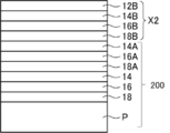
- FIGS. 4 and 5 show an example of manufacturing the wiring substrate 100 in which one set of laminates (the solvent permeation layer 18, the receiving layer 16, the protective layer 14 on which the wiring pattern is formed) is stacked on the substrate P.
- a wiring board (multilayer wiring board) in which two or more sets of laminates are stacked on the substrate P may be manufactured. That is, as another embodiment of the present manufacturing method, a new transfer film having a wiring pattern obtained in the above wiring pattern forming step is attached on the wiring substrate obtained in the above peeling step, The method of peeling a support body in a new transfer film may be repeated to obtain a wiring substrate such that a plurality of wiring patterns are stacked on the substrate. Thereby, a wiring board (multilayer wiring board) in which a plurality of wiring patterns are stacked on the substrate can be obtained.
- a new transfer film X1 on which a wiring pattern is formed which is obtained by the above-described wiring pattern formation process, is prepared (preparation process).
- the transfer film X1 is formed by sequentially laminating a protective layer 14A, a receiving layer 16A, and a solvent permeation layer 18A in which a wiring pattern is formed on one surface of a support 12A.
- the solvent permeable layer 18A of the transfer film X1 is brought into contact with the protective layer 14 of the wiring substrate 100 obtained by the peeling process described in FIG. 5 to bond the transfer film X1 and the wiring substrate 100 (transfer Sticking process of film X1, see FIG. 6).
- the support 12A is peeled off from the transfer film X1 (peeling process using the transfer film X1, see FIG. 7).
- the wiring board 200 in which two laminates each having a wiring pattern are stacked on the substrate P can be obtained.
- the transfer film X2 is formed by sequentially laminating a protective layer 14B, a receiving layer 16B, and a solvent permeation layer 18B in which a wiring pattern is formed on one surface of a support 12B.
- the solvent permeable layer 18B of the transfer film X2 is brought into contact with the protective layer 14A of the wiring substrate 200, and the transfer film X2 and the wiring substrate 200 are attached (transfer film Sticking process using X2, see FIG. 8).
- the support 12B is peeled off from the transfer film X2 (peeling process using the transfer film X2, see FIG. 9).
- the wiring board 300 in which three laminates each having a wiring pattern are stacked on the substrate P is obtained.
- the wiring board obtained by the present manufacturing method holds the security of card materials such as, for example, riding cards such as trains and buses, credit cards, electronic money cards, identification (ID) cards, card keys, various point cards, etc. It is suitably used for forming an electronic circuit, a complex radio frequency (RF) chip for enhancing confidentiality of various information, and an antenna circuit for energy harvesting.
- the wiring substrate is preferably a thin film.
- the stirring speed was changed to 100 rpm, and the temperature was maintained at 135 ° C. for 3.0 hours to complete heating, and natural cooling was continued until the temperature reached 80 ° C. or less.
- a part of the solution (slurry after reaction) was separated into a centrifuge tube, washed by adding distilled water, and centrifuged at 3000 rpm for 5 minutes. After removing the supernatant after centrifugation, methanol was added to wash the precipitate, and the methanol dispersion was centrifuged at 2500 rpm for 5 minutes.
- the major axis average length and the minor axis average length are calculated using a transmission electron microscope (TEM), and the aspect ratio (major axis average length is calculated based on the obtained values. / Short axis average length) was calculated. Each value is shown in Table 1.
- [Production of conductive ink] 20 ml of ethylene glycol and 5 ml of ethanol were added to 75 ml of the dispersion of silver nanowire (A) to prepare a conductive ink 1. After preparation, ultrasonic dispersion was carried out for 20 minutes, and then stirring was carried out at 2500 rpm for 20 minutes using “T 18 digital ULTRA-TURRAX” (trade name) manufactured by IKA Corporation to complete redispersion.
- the viscosity of the conductive ink 1 was 15 mPa ⁇ s (25 ° C.) or less. The viscosity was measured by "VISCOMATE VM-1G" (trade name) manufactured by CBC Materials.
- [Conductive ink 2] In 75 ml of a dispersion of silver nanowire (A), 20 mg of ethylene glycol and 15 mg of a compound represented by the following formula (I-1) (gold thioglucose) are dissolved in 5 ml of ethanol to prepare metal nano for gold thioglucose.
- the conductive ink 2 was prepared by adding the mass ratio of the wire to 100. The other operations were the same as in the case of the conductive ink 1 to obtain a conductive ink 2.
- the viscosity of the conductive ink 2 was 15 mPa ⁇ s (25 ° C.) or less (measured under the same conditions as the conductive ink 1).
- a conductive ink 3 was obtained in the same manner as the conductive ink 2 except that the dispersion of silver nanowires (B) was used instead of the dispersion of silver nanowires (A).
- the viscosity of the conductive ink 3 was 17 mPa ⁇ s (25 ° C.) or less (measured under the same conditions as the conductive ink 1).
- a conductive ink 4 was obtained in the same manner as the conductive ink 2 except that the dispersion of the silver nanowire (C) was used instead of the dispersion of the silver nanowire (A).
- the viscosity of the conductive ink 4 was 17 mPa ⁇ s (25 ° C.) or less (measured under the same conditions as the conductive ink 1).
- a conductive ink 5 was obtained in the same manner as the conductive ink 2 except that 1.5 g of solid magnetic fluid (MSG-W11, manufactured by FeroTec) was added.
- MSG-W11 is an aqueous liquid medium in which magnetic particles (mixture of magnetite (Fe 3 O 4 ) particles and maghemite ( ⁇ -Fe 2 O 3 ) particles) are dispersed, and the average particle diameter is 10 nm. It is.
- the viscosity of the conductive ink 5 was 17 mPa ⁇ s (25 ° C.) or less (measured under the same conditions as the conductive ink 1).
- Conductive ink 6 Silver nanoparticle ink (trade name “NBSIJ-MU01”) manufactured by Mitsubishi Paper Industries, Ltd. was used as the conductive ink 6. The viscosity of the conductive ink 6 was 2.3 mPa ⁇ s (25 ° C.) or less (measured under the same conditions as the conductive ink 1).
- a conductive ink 7 is used in the same manner as the conductive ink 2 except that a compound represented by the following formula (II) is used instead of the compound (gold thioglucose) represented by the above formula (I-1). I got The viscosity of the conductive ink 7 was 17 mPa ⁇ s (25 ° C.) or less (measured under the same conditions as the conductive ink 1).
- a conductive ink 8 is obtained in the same manner as the conductive ink 2 except that the weight ratio of the metal nanowire to the compound (gold thioglucose) represented by the above formula (I-1) is 11
- the viscosity of the conductive ink 8 was 17 mPa ⁇ s (25 ° C.) or less (measured under the same conditions as the conductive ink 1).
- a conductive ink 9 is obtained in the same manner as the conductive ink 2 except that the mass ratio of the metal nanowire to the compound (gold thioglucose) represented by the above formula (I-1) is 999.
- the viscosity of the conductive ink 9 was 17 mPa ⁇ s (25 ° C.) or less (measured under the same conditions as the conductive ink 1).
- Transfer film A was produced as follows.
- a PET film having a width of 1000 mm, a thickness of 100 ⁇ m, and a length of 100 m (trade name “Cosmo Shine A4100” manufactured by Toyobo Co., Ltd.) was used.
- a coating solution for forming a protective layer is coated at 35 g / m 2 on a highly smooth surface of the support 12 using a # 20 wire bar, and dried at 100 ° C. for 2 minutes.
- the protective layer 14 was formed on the surface.
- the thickness of the formed protective layer 14 was 3 ⁇ m.
- the coating liquid for forming the receiving layer and the inline liquid were inline mixed and applied to the surface of the protective layer 14 previously formed, using an extrusion die coater. Specifically, the receiving layer 90.5 g / m 2 coating solution for forming a (coating amount), and line mixing inline solution 7.4 g / m 2 (coated amount) was applied.
- the formed coating layer (coating film) was dried at 80 ° C. (wind speed 5 m / sec) by a hot air dryer until the solid content concentration became 36 mass%. During this time, the coated layer showed constant drying.
- the coating layer is immersed for 3 seconds in a solution containing a basic compound, and a solution containing a basic compound is applied onto the coating layer with a solid content concentration of 36% by mass. 13 g / m 2 was attached. Furthermore, it dried at 72 degreeC for 10 minutes, and formed the receptive layer 16 in the surface of the protective layer 14. The thickness of the formed receiving layer 16 was 20 ⁇ m.
- a coating solution for forming a solvent-permeable layer is applied to the surface of the receptor layer 16 previously formed using a # 8 wire bar, and dried at 40 ° C. for 10 minutes.
- the solvent permeation layer 18 was formed to prepare a transfer film 10.
- a transfer film is formed in the same manner as in the production of the transfer film A, except that the receiving layer 16 formed using the following materials is formed instead of the receiving layer 16 of the transfer film A and the solvent permeation layer 18 is not formed.
- the receiving layer of the transfer film B was formed as follows. First, an inkjet receptive layer resin (trade name "NS-310X” manufactured by Takamatsu Yushi Co., Ltd., a swelling type receptive layer) was prepared. Next, the surface of the protective layer 14 was coated with the above-mentioned ink jet receiving layer resin at a coating amount of 70 g / m 2 using an extrusion die coater. Thereafter, it was dried at 120 ° C. for 5 minutes to form the receptive layer 16 on the surface of the protective layer 14. The thickness of the obtained receptive layer 16 was 9 ⁇ m.
- Example 1 First, using an inkjet recording apparatus, transfer film is printed by using the conductive ink 1 from the side opposite to the side on which the support 12 is formed in the transfer film A (that is, the solvent permeation layer 18). A wiring pattern was formed on 10 (wiring pattern formation step). Next, the surface on the opposite side to the surface on which the support 12 is formed in the transfer film 10 on which the wiring pattern is formed (that is, the solvent permeation layer 18) is brought into contact with the substrate P, and the transfer film 10 and the substrate P Stacked. Next, the transfer film 10 and the substrate P were pressed and heated from the side of the support 12 to thermally bond the transfer film 10 (solvent permeation layer 18) and the substrate P (adhesion step). In addition, the heating temperature of the transfer film 10 at the time of sticking was 120 degreeC. Next, the support 12 was peeled off from the transfer film 10 attached to the substrate P (peeling step). Thus, the wiring board in Example 1 was manufactured.
- Example 2 to 6 Wiring boards in Examples 2 to 6 were manufactured in the same manner as Example 1 except that conductive inks 2 to 6 were used instead of the conductive ink 1, respectively. However, in Example 5, the conductive ink 5 was discharged while applying a magnetic field so that the magnetic particles were arranged in the discharge direction of the discharge head of the ink jet recording apparatus.
- Example 7 The wiring board in Example 7 is manufactured in the same manner as in Example 6 except that the wiring pattern is exposed to UV (ultraviolet) radiation using PulseForge 3300 (trade name, manufactured by Novacentrix) before the transfer step. did. As the exposure conditions, 3 J / cm 2 of Pulse light (1400 ⁇ Sec) was irradiated 10 times.
- Example 8 The wiring board in Example 8 is manufactured in the same manner as in Example 2 except that the wiring pattern is exposed to UV (ultraviolet) irradiation using PulseForge 3300 (trade name, manufactured by Novacentrix) before the transfer step. did. As the exposure conditions, 3 J / cm 2 of Pulse light (1400 ⁇ Sec) was irradiated 10 times.
- Example 9 A wiring board in Example 9 was manufactured in the same manner as Example 2 except that transfer film B was used instead of transfer film A.
- transfer film B was used instead of transfer film A.
- the wiring pattern forming step using the transfer film B printing using the conductive ink 1 from the side of the transfer film B opposite to the side on which the support 12 is formed (that is, the receiving layer 16) Did.
- the surface (that is, the receiving layer 16) opposite to the surface on which the support 12 is formed in the transfer film 10 on which the wiring pattern is formed is brought into contact with the substrate P.
- the resistance value of the wiring board in each example was measured. Specifically, the discharge amount is set so that the amount of silver in the conductive ink to be applied is 1.5 g / m 2, and the wiring substrate in each example having a wiring pattern of width 5 mm ⁇ length 50 mm is manufactured. The resistance values at both ends of the wiring board were measured using a digital multimeter RD701 (trade name, manufactured by Sanwa Electric Instruments Co., Ltd.).
- the durability of the wiring board in each example was evaluated. Specifically, first, the discharge amount is set so that the silver amount in the conductive ink to be applied is 1.5 g / m 2, and the wiring substrate in each example having a wiring pattern of 5 mm wide ⁇ 50 mm long is used. Manufactured. The obtained wiring board was stored for 5 days under conditions of 85 ° C. and 85% RH. The resistance value of the wiring board before and after storage was measured by a digital multimeter RD701 (trade name, manufactured by Sanwa Electric Instruments Co., Ltd.). Assuming that the resistance before storage is R0 and the resistance after storage is R, the rate of change in resistance before and after storage was calculated according to the following equation.
- Example 1 In the manufacturing method of the wiring board in an example, it printed on the specific transfer film in which the protective layer was formed beforehand. Therefore, the process of forming a protective layer was unnecessary between the wiring pattern formation process and the adhesion process, and the process from printing to adhesion could be smoothly performed.
- Example 2 Example 11, and Example 12
- Example 12 when a conductive ink containing the compound represented by Formula (I-1) is used (Example 2, Example 11, and Example) Example 12) showed that the durability of the wiring board is excellent.
- Example 2 to 4 when the aspect ratio of the conductive substance (silver nanowire) is 200 or more (Examples 2 and 4), the wiring having a low resistance value and a wiring excellent in conductivity A substrate was shown to be obtained.
- Example 2 it was shown that when the conductive ink containing magnetic particles is used (Example 5), the ejection suitability of the ink jet recording apparatus is excellent. Further, from the comparison between Example 1 and Example 6, it was shown that when the metal nanowires were used (Example 1), the resistance value of the wiring pattern was low and the durability of the wiring board was also excellent. Also, from the comparison between Example 6 and Example 7 and the comparison between Example 2 and Example 8, when the exposure of the wiring pattern is carried out (Example 7 and Example 8), the resistance value of the wiring pattern is It was shown to go low.
- Example 2 From the comparison between Example 2 and Example 9, it was shown that the resistance value of the wiring pattern is lowered when the transfer film A having the receiving layer containing the receiving particles is used (Example 2). Further, from the comparison between Example 2 and Example 10, when the compound represented by the formula (I-1) is used as the migration inhibitor (Example 2), the durability of the wiring board is more excellent, and the wiring The resistance of the pattern was also shown to be low.
- a conductive ink 6 was prepared in the same manner as the conductive ink 1 except that 1 g of a dye (Direct Blue 87) was added to the conductive ink 1.
- a dye Direct Blue 87
- the evaluations of the ejection stability, the resistance value and the durability were all the same as in Example 1.
- the wiring board was visually confirmed, the colored wiring pattern was able to be confirmed.
Landscapes
- Engineering & Computer Science (AREA)
- Chemical & Material Sciences (AREA)
- Manufacturing & Machinery (AREA)
- Microelectronics & Electronic Packaging (AREA)
- Wood Science & Technology (AREA)
- Materials Engineering (AREA)
- Life Sciences & Earth Sciences (AREA)
- Organic Chemistry (AREA)
- Nanotechnology (AREA)
- Dispersion Chemistry (AREA)
- Manufacturing Of Printed Wiring (AREA)
- Conductive Materials (AREA)
- Parts Printed On Printed Circuit Boards (AREA)
- Inks, Pencil-Leads, Or Crayons (AREA)
Abstract
The present invention addresses the problem of providing: a wiring board production method that makes it possible to conveniently produce a wiring board; and a conductive ink. This wiring board production method uses a transfer film that has: a support body; a protective layer that is formed on one surface of the support body and can be removed from the support body; and a receiving layer that is formed on the surface of the protective layer and receives the solvent of a conductive ink that includes the solvent and a conductive substance. The production method includes: a wiring pattern formation step that is for forming a wiring pattern on the transfer film by using the conductive ink to print onto a surface of the transfer film that is on the opposite side from the surface on which the support body is formed; a bonding step that is after the wiring pattern formation step and is for bringing the surface on which the wiring pattern has been formed, i.e., the surface of the transfer film that is on the opposite side from the surface on which the support body is formed, into contact with a substrate and bonding the transfer film and the substrate; and a removal step that is after the bonding step and is for obtaining a wiring board by removing the support body from the transfer film that has been bonded to the substrate.
Description
本発明は、配線基板の製造方法および導電性インクに関する。
The present invention relates to a method of manufacturing a wiring substrate and a conductive ink.
基板上に配線パターンが形成された配線基板が知られている。このような配線パターンの形成方法の具体例としては、基板上に設けられた金属層をエッチングして配線パターンを形成する方法、導電ペーストまたは導電性インクを用いて配線パターンを形成する方法、および、無電解めっき法により配線パターンを形成する方法が挙げられる。
A wiring board in which a wiring pattern is formed on a substrate is known. As a specific example of a method of forming such a wiring pattern, a method of forming a wiring pattern by etching a metal layer provided on a substrate, a method of forming a wiring pattern using a conductive paste or a conductive ink, and And a method of forming a wiring pattern by electroless plating.
これらの方法のうち、特許文献1には、導電性インクを用いた配線パターンの製造方法(配線基板の製造方法)が示されている。具体的には、支持フィルム、接着層、導電性インクを用いて得られた導電層(配線パターン)、および、保護層がこの順に積層された転写フィルムから支持フィルムを剥離した後、接着層を介して導電層を基板上に接着する方法が示されている(請求項1、請求項4等)。
Among these methods, Patent Document 1 shows a method of manufacturing a wiring pattern using a conductive ink (a method of manufacturing a wiring substrate). Specifically, after peeling the support film from the transfer film on which the support film, the adhesive layer, the conductive layer (wiring pattern) obtained using the conductive ink, and the protective layer are laminated in this order, the adhesive layer is removed. A method of bonding the conductive layer on the substrate via the substrate is disclosed (claims 1, 4 and the like).
しかしながら、上記特許文献1に記載の配線基板の製造方法は、配線パターン形成工程後、転写フィルムと基板との貼着工程前に、配線パターンを保護する保護層を形成する必要がある。そのため、配線パターン形成工程から貼着工程までの工程をスムーズに実施できず、工程が煩雑になるという問題がある。
そこで、本発明は、配線基板を簡便に製造できる配線基板の製造方法、および、導電性インクの提供を課題とする。 However, in the method of manufacturing a wiring board described in Patent Document 1, it is necessary to form a protective layer for protecting the wiring pattern after the step of forming the wiring pattern and before the step of attaching the transfer film to the substrate. Therefore, the process from the wiring pattern formation process to the affixing process can not be performed smoothly, and there is a problem that a process becomes complicated.
Then, this invention makes it a subject to provide the manufacturing method of the wiring board which can manufacture a wiring board simply, and a conductive ink.
本発明者は、上記課題について鋭意検討した結果、支持体、保護層、受容層がこの順に積層された特定の転写フィルムに対して、支持体とは反対側の面から導電性インクを用いた印刷を行い、得られた転写フィルムを用いて配線基板を簡便に製造できるのを見出し、本発明に至った。
すなわち、本発明者は、以下の構成により上記課題が解決できることを見出した。 As a result of intensive studies on the above problems, the inventor used a conductive ink from the side opposite to the support for a specific transfer film in which the support, the protective layer, and the receiving layer were laminated in this order. It has been found that printing can be performed and wiring boards can be easily manufactured using the obtained transfer film, and the present invention has been achieved.
That is, the present inventor has found that the above problem can be solved by the following configuration.
[1]
支持体と、
上記支持体の一方の表面に形成され上記支持体から剥離可能な保護層と、
上記保護層の表面に形成され、導電性物質および溶剤を含む導電性インク中の上記溶剤を受容する受容層と、
を有する転写フィルムを用いた配線基板の製造方法であって、
上記転写フィルムにおける上記支持体が形成された面とは反対側の面からの上記導電性インクを用いた印刷によって、上記転写フィルムに配線パターンを形成する配線パターン形成工程と、
上記配線パターン形成工程後、上記配線パターンが形成された上記転写フィルムにおける上記支持体が形成された面とは反対側の面を基板に当接して、上記転写フィルムと上記基板とを貼着する貼着工程と、
上記貼着工程後、上記基板に貼着された上記転写フィルムから上記支持体を剥離して、配線基板を得る剥離工程と、
を有する、配線基板の製造方法。
[2]
上記転写フィルムは、上記受容層の表面に形成され、上記溶剤を浸透させる空隙を有する溶剤浸透層をさらに有する、[1]に記載の配線基板の製造方法。
[3]
上記印刷が、インクジェット法により実施される、[1]または[2]に記載の配線基板の製造方法。
[4]
上記貼着工程が加熱下で実施される、[1]~[3]のいずれか1つに記載の配線基板の製造方法。
[5]
上記貼着工程における加熱温度が、80℃以上である、[4]に記載の配線基板の製造方法。
[6]
上記剥離工程にて得られる上記配線基板上に、上記配線パターン形成工程によって得られる配線パターンが形成された新たな転写フィルムを貼着した後、上記新たな転写フィルム中の支持体を剥離する手順を、上記基板上に複数の配線パターンが積層されるように、繰り返す、[1]~[5]のいずれか1つに記載の配線基板の製造方法。
[7]
上記配線パターン形成工程後に、上記配線パターンを露光する、[1]~[6]のいずれか1つに記載の配線基板の製造方法。
[8]
上記導電性物質が、アスペクト比200以上の金属ナノワイヤーである、[1]~[7]のいずれか1つに記載の配線基板の製造方法。
[9]
上記導電性インクが、後述の式(I)で表される化合物をさらに含む、[1]~[8]のいずれか1つに記載の配線基板の製造方法。
後述の式(I)中、Xは、金原子、パラジウム原子または白金原子を表す。
[10]
上記導電性物質がアスペクト比200以上の金属ナノワイヤーであり、
上記式(I)で表される化合物に対する上記金属ナノワイヤーの質量比が、10超1000未満である、[9]に記載の配線基板の製造方法。
[11]
上記導電性インクが、磁性粒子をさらに含む、[1]~[10]のいずれか1つに記載の配線基板の製造方法。
[12]
上記導電性インクが、色材をさらに含む、[1]~[11]のいずれか1つに記載の配線基板の製造方法。
[13]
溶剤と、後述の式(I)で表される化合物と、アスペクト比が200以上である金属ナノワイヤーと、を含む、導電性インク。
後述の式(I)中、Xは、金原子、パラジウム原子または白金原子を表す。
[14]
上記式(I)で表される化合物に対する上記金属ナノワイヤーの質量比が、10超1000未満である、[13]に記載の導電性インク。
[15]
さらに、磁性粒子を含む、[13]または[14]に記載の導電性インク。
[16]
さらに、色材を含む、[13]~[15]のいずれか1つに記載の導電性インク。 [1]
A support,
A protective layer formed on one surface of the support and releasable from the support;
A receiving layer formed on the surface of the protective layer and receiving the solvent in a conductive ink containing a conductive substance and a solvent;
A method of manufacturing a wiring substrate using a transfer film having
A wiring pattern forming step of forming a wiring pattern on the transfer film by printing using the conductive ink from the surface of the transfer film opposite to the surface on which the support is formed;
After the step of forming the wiring pattern, the surface opposite to the surface on which the support is formed in the transfer film on which the wiring pattern is formed is brought into contact with the substrate to bond the transfer film and the substrate Sticking process,
A peeling step of obtaining a wiring substrate by peeling the support from the transfer film stuck to the substrate after the sticking step;
A method of manufacturing a wiring board, comprising:
[2]
The method for producing a wiring board according to [1], wherein the transfer film further has a solvent permeation layer formed on the surface of the receiving layer and having a void through which the solvent is allowed to permeate.
[3]
The method for producing a wiring board according to [1] or [2], wherein the printing is performed by an inkjet method.
[4]
The method for producing a wiring board according to any one of [1] to [3], wherein the sticking step is performed under heating.
[5]
The manufacturing method of the wiring board as described in [4] whose heating temperature in the said adhesion | pasting process is 80 degreeC or more.
[6]
A procedure of peeling a support in the new transfer film after sticking a new transfer film on which the wiring pattern obtained in the wiring pattern formation step is formed on the wiring substrate obtained in the peeling step The method of manufacturing a wiring board according to any one of [1] to [5], wherein a plurality of wiring patterns are stacked on the substrate.
[7]
The method of manufacturing a wiring board according to any one of [1] to [6], wherein the wiring pattern is exposed after the step of forming the wiring pattern.
[8]
The method for producing a wiring board according to any one of [1] to [7], wherein the conductive substance is a metal nanowire having an aspect ratio of 200 or more.
[9]
The method for producing a wiring board according to any one of [1] to [8], wherein the conductive ink further comprises a compound represented by the formula (I) described later.
In the following formula (I), X represents a gold atom, a palladium atom or a platinum atom.
[10]
The conductive material is a metal nanowire having an aspect ratio of 200 or more,
The manufacturing method of the wiring board as described in [9] whose mass ratio of the said metal nanowire with respect to the compound represented by the said Formula (I) is more than 10 and less than 1000.
[11]
The method for producing a wiring board according to any one of [1] to [10], wherein the conductive ink further includes magnetic particles.
[12]
The method for producing a wiring board according to any one of [1] to [11], wherein the conductive ink further contains a colorant.
[13]
A conductive ink comprising a solvent, a compound represented by Formula (I) described later, and a metal nanowire having an aspect ratio of 200 or more.
In the following formula (I), X represents a gold atom, a palladium atom or a platinum atom.
[14]
The conductive ink according to [13], wherein a mass ratio of the metal nanowire to the compound represented by the formula (I) is more than 10 and less than 1,000.
[15]
Furthermore, the conductive ink according to [13] or [14], which further comprises magnetic particles.
[16]
Furthermore, the conductive ink according to any one of [13] to [15], further comprising a coloring material.
以下に示すように、本発明によれば、絶縁層で保護された配線基板を簡便に製造できる配線基板の製造方法、および、導電性インクを提供できる。特に、本発明によれば、現像、エッチングおよび焼成等のプロセスが不要な配線基板の製造方法を提供できる。
As described below, according to the present invention, it is possible to provide a method of manufacturing a wiring board capable of easily manufacturing a wiring board protected by an insulating layer, and a conductive ink. In particular, according to the present invention, it is possible to provide a method of manufacturing a wiring substrate which does not require processes such as development, etching and baking.
以下に、本発明について説明する。
以下に記載する構成要件の説明は、本発明の代表的な実施態様に基づいてなされることがあるが、本発明はそのような実施態様に限定されるものではない。
本発明において「~」を用いて表される数値範囲は、「~」の前後に記載される数値を下限値および上限値として含む範囲を意味する。
本発明において「(メタ)アクリル」とは、「アクリル」および「メタクリル」の総称を意味する。 The present invention will be described below.
Although the description of the configuration requirements described below may be made based on the representative embodiments of the present invention, the present invention is not limited to such embodiments.
The numerical range represented using “to” in the present invention means a range including the numerical values described before and after “to” as the lower limit value and the upper limit value.
In the present invention, "(meth) acrylic" means a generic name of "acrylic" and "methacrylic".
本発明の配線基板の製造方法(以下、「本製造方法」ともいう。)は、支持体と、上記支持体の一方の表面に形成され上記支持体から剥離可能な保護層と、上記保護層の表面に形成され、導電性物質および溶剤を含む導電性インク中の上記溶剤を受容する受容層と、を有する転写フィルム(以下、「特定転写フィルム」ともいう。)を用いた配線基板の製造方法である。
また、本製造方法は、上記転写フィルムにおける上記支持体が形成された面とは反対側の面からの上記導電性インクを用いた印刷によって、上記特定転写フィルムに配線パターンを形成する配線パターン形成工程と、
上記配線パターン形成工程後、上記配線パターンが形成された上記特定転写フィルムの上記支持体が形成された面とは反対側の面を基板に当接して、上記特定転写フィルムと上記基板とを貼着する貼着工程と、
上記貼着工程後、上記基板に貼着された上記特定転写フィルムから上記支持体を剥離して、配線基板を得る剥離工程と、を有する。
本製造方法では、保護層が予め形成された特定転写フィルムに印刷を行うので、配線パターン形成工程と貼着工程との間に保護層を形成する工程が不要となり、印刷から貼着までの工程をスムーズに実施できる。このように、本製造方法によれば、簡便な工程で配線基板を製造できる。さらに、本製造方法によれば、現像、エッチングおよび焼成できないもの、例えば、装置等の表面に直接、配線を貼着できる。
以下では、まず、本製造方法で使用される材料について詳述し、その後、各工程について詳述する。 The method for producing a wiring substrate of the present invention (hereinafter, also referred to as “the present production method”) comprises a support, a protective layer formed on one surface of the support and removable from the support, and the protective layer. Production of a wiring substrate using a transfer film (hereinafter, also referred to as "specific transfer film") having a receptor layer formed on the surface of the conductive ink and containing the above-mentioned solvent in the conductive ink containing the conductive substance and the solvent. It is a method.
In addition, according to the present manufacturing method, a wiring pattern is formed on the specific transfer film by printing using the conductive ink from the surface of the transfer film opposite to the surface on which the support is formed. Process,
After the step of forming the wiring pattern, the surface opposite to the surface on which the support is formed of the specific transfer film on which the wiring pattern is formed is brought into contact with the substrate to attach the specific transfer film and the substrate The sticking process to wear,
After the sticking step, the step of peeling the support from the specific transfer film stuck to the substrate to obtain a wiring board is provided.
In the present manufacturing method, since printing is performed on the specific transfer film on which the protective layer is formed in advance, the process of forming the protective layer is not necessary between the wiring pattern forming process and the adhering process, and the process from printing to adhering Can be implemented smoothly. As described above, according to the present manufacturing method, the wiring substrate can be manufactured by a simple process. Furthermore, according to the present manufacturing method, the wiring can be directly stuck to the surface which can not be developed, etched and fired, for example, the apparatus.
Below, the material used by this manufacturing method is explained in full detail first, and, after that, each process is explained in full detail.
[特定転写フィルム]
本製造方法で使用する特定転写フィルムは、支持体と、上記支持体の一方の表面に形成され上記支持体から剥離可能な保護層と、上記保護層の表面に形成され、導電性物質および溶剤を含む導電性インク中の上記溶剤を受容する受容層と、を有する。
特定転写フィルムは、上記受容層の表面に形成され、上記導電性インク中の上記溶剤を浸透させる空隙を有する溶剤浸透層を有していてもよい。
以下においては、特定転写フィルムが溶剤浸透層を有する場合を例にして、図面を参照しながら特定転写フィルムについて詳述する。 [Specific transfer film]
The specific transfer film used in this production method is formed on a support, a protective layer formed on one surface of the support and removable from the support, and a surface of the protective layer, and a conductive substance and a solvent. And a receptive layer for receiving the solvent in the conductive ink.
The specific transfer film may have a solvent permeable layer formed on the surface of the receptive layer and having a void through which the solvent in the conductive ink can penetrate.
In the following, the specific transfer film will be described in detail with reference to the drawings, taking the case where the specific transfer film has a solvent permeable layer as an example.
図1は、特定転写フィルムの一例を模式的に示す断面図である。図1に示すように、転写フィルム10は、支持体12と、支持体12の一方の表面に形成される保護層14と、保護層14の表面に形成される受容層16と、受容層16の表面に形成される溶剤浸透層18と、を有する。
後に詳述するが、転写フィルム10は、溶剤浸透層18側から導電性インクを用いた印刷が行われた後、溶剤浸透層18が基板Pに貼着され、その後、支持体12が保護層14から剥離されることにより、溶剤浸透層18、受容層16および保護層14からなる積層体が基板Pに転写され、基板Pに配線パターンを形成する。
したがって、溶剤浸透層18、受容層16および保護層14からなる積層体が基板Pに転写された状態では、保護層14が表面になり、溶剤浸透層18が基板P側になる。 FIG. 1 is a cross-sectional view schematically showing an example of the specific transfer film. As shown in FIG. 1, thetransfer film 10 comprises a support 12, a protective layer 14 formed on one surface of the support 12, a receptive layer 16 formed on the surface of the protective layer 14, and a receptive layer 16 And a solvent permeation layer 18 formed on the surface of
As will be described in detail later, after thetransfer film 10 is printed using the conductive ink from the solvent permeation layer 18 side, the solvent permeation layer 18 is adhered to the substrate P, and then the support 12 is a protective layer By peeling from the substrate 14, the laminate including the solvent permeation layer 18, the receiving layer 16 and the protective layer 14 is transferred to the substrate P, and a wiring pattern is formed on the substrate P.
Therefore, in a state in which the laminate including thesolvent permeation layer 18, the receiving layer 16 and the protective layer 14 is transferred to the substrate P, the protective layer 14 becomes the surface and the solvent permeation layer 18 becomes the substrate P side.
後に詳述するが、転写フィルム10は、溶剤浸透層18側から導電性インクを用いた印刷が行われた後、溶剤浸透層18が基板Pに貼着され、その後、支持体12が保護層14から剥離されることにより、溶剤浸透層18、受容層16および保護層14からなる積層体が基板Pに転写され、基板Pに配線パターンを形成する。
したがって、溶剤浸透層18、受容層16および保護層14からなる積層体が基板Pに転写された状態では、保護層14が表面になり、溶剤浸透層18が基板P側になる。 FIG. 1 is a cross-sectional view schematically showing an example of the specific transfer film. As shown in FIG. 1, the
As will be described in detail later, after the
Therefore, in a state in which the laminate including the
(支持体)
支持体12は、転写フィルム10が基板Pに貼着されるまで、保護層14、受容層16および溶剤浸透層18を支持するものである。 (Support)
Thesupport 12 supports the protective layer 14, the receptive layer 16 and the solvent permeation layer 18 until the transfer film 10 is adhered to the substrate P.
支持体12は、転写フィルム10が基板Pに貼着されるまで、保護層14、受容層16および溶剤浸透層18を支持するものである。 (Support)
The
支持体12は、保護層14、受容層16および溶剤浸透層18を支持できる公知の各種のシート状物(フィルム)が利用可能である。特に、後述する貼着工程が加熱下で実施される場合(すなわち、加熱貼着の場合)には、十分な耐熱性を有する支持体12を用いるのが好ましい。
支持体12の具体例としては、各種の樹脂材料で形成される樹脂フィルムが挙げられる。支持体12となる樹脂材料の具体例としては、ポリエチレンテレフタレート(PET(polyethylene terephthalate))およびポリエチレンナフタレート(PEN(polyethylene naphthalate))等のポリエステル樹系脂、ポリカーボネート樹脂、アクリル樹脂、メタクリル樹脂、および、ポリイミド樹脂が挙げられる。 As thesupport 12, various known sheet materials (films) capable of supporting the protective layer 14, the receptive layer 16 and the solvent permeation layer 18 can be used. In particular, when the sticking step described later is carried out under heating (that is, in the case of heat sticking), it is preferable to use the support 12 having sufficient heat resistance.
Specific examples of thesupport 12 include resin films formed of various resin materials. Specific examples of the resin material to be the support 12 include polyester resins such as polyethylene terephthalate (PET (polyethylene terephthalate)) and polyethylene naphthalate (PEN (polyethylene naphthalate)), polycarbonate resins, acrylic resins, methacrylic resins, and And polyimide resins.
支持体12の具体例としては、各種の樹脂材料で形成される樹脂フィルムが挙げられる。支持体12となる樹脂材料の具体例としては、ポリエチレンテレフタレート(PET(polyethylene terephthalate))およびポリエチレンナフタレート(PEN(polyethylene naphthalate))等のポリエステル樹系脂、ポリカーボネート樹脂、アクリル樹脂、メタクリル樹脂、および、ポリイミド樹脂が挙げられる。 As the
Specific examples of the
支持体12の厚さは、特に限定されないが、後述の貼着工程を行う前まで保護層14、受容層16および溶剤浸透層18を支持でき、かつ、基板Pに転写フィルム10を貼着した後、破断等を生じることなく適正に剥離できる厚さを、形成材料等に応じて、適宜、設定すればよい。
具体的には、支持体12の厚さは、20~200μmが好ましく、50~130μmがより好ましい。 The thickness of thesupport 12 is not particularly limited, but the protective layer 14, the receptive layer 16 and the solvent permeation layer 18 can be supported until the adhesion process described later is performed, and the transfer film 10 is adhered to the substrate P After that, a thickness that can be properly peeled without causing breakage or the like may be appropriately set according to the forming material or the like.
Specifically, the thickness of thesupport 12 is preferably 20 to 200 μm, and more preferably 50 to 130 μm.
具体的には、支持体12の厚さは、20~200μmが好ましく、50~130μmがより好ましい。 The thickness of the
Specifically, the thickness of the
(保護層)
保護層14は、支持体12の一方の表面に形成される。
保護層14は、後述の剥離工程後に、受容層16を保護する層である。 (Protective layer)
Protective layer 14 is formed on one surface of support 12.
Theprotective layer 14 is a layer that protects the receptive layer 16 after the peeling process described later.
保護層14は、支持体12の一方の表面に形成される。
保護層14は、後述の剥離工程後に、受容層16を保護する層である。 (Protective layer)
The
保護層14は、ポリマーを含むのが好ましい。
保護層14に含まれ得るポリマーのガラス転移温度(Tg)は、0℃以上が好ましく、20℃以上がより好ましく、30℃以上がさらに好ましい。上記ポリマーのTgが0℃以上であれば、後述の剥離工程において、支持体12と保護層14との剥離性がより向上する。
保護層14に含まれる得るポリマーのTgの上限値は、80℃以下が好ましい。上記ポリマーのTgが80℃以下であれば、保護層14が良好に形成(造膜)されること、造膜温度を下げられるため、支持体12の選択範囲が広がること、などの利点がある。
なお、ポリマーのTgは、公知の方法で測定してもよく、各種の文献に記載されている数値を用いてもよく、市販品のポリマーを用いる場合には、カタログ等に記載されている数値を用いてもよく、ポリマーの組成から算出した数値を用いてもよい。ガラス転移温度の測定方法の具体例としては、示差走査熱量分析によって、JIS(Japanese Industrial Standards) K 7121に準拠して測定する方法が挙げられる。 Theprotective layer 14 preferably comprises a polymer.
0 degreeC or more is preferable, as for the glass transition temperature (Tg) of the polymer which may be contained in the protective layer 14, 20 degreeC or more is more preferable, and 30 degreeC or more is more preferable. When the Tg of the polymer is 0 ° C. or higher, the releasability between the support 12 and the protective layer 14 is further improved in the peeling step described later.
The upper limit of the Tg of the polymer that can be contained in theprotective layer 14 is preferably 80 ° C. or less. If the Tg of the above-mentioned polymer is 80 ° C. or less, the protective layer 14 can be favorably formed (film-formed), and since the film-forming temperature can be lowered, the selection range of the support 12 can be expanded. .
The Tg of the polymer may be measured by a known method, or the numerical values described in various documents may be used, and when using a commercially available polymer, the numerical values described in the catalog etc. Or a numerical value calculated from the composition of the polymer. As a specific example of the measuring method of glass transition temperature, the method of measuring based on JIS (Japanese Industrial Standards) K7121 by a differential scanning calorimetry is mentioned.
保護層14に含まれ得るポリマーのガラス転移温度(Tg)は、0℃以上が好ましく、20℃以上がより好ましく、30℃以上がさらに好ましい。上記ポリマーのTgが0℃以上であれば、後述の剥離工程において、支持体12と保護層14との剥離性がより向上する。
保護層14に含まれる得るポリマーのTgの上限値は、80℃以下が好ましい。上記ポリマーのTgが80℃以下であれば、保護層14が良好に形成(造膜)されること、造膜温度を下げられるため、支持体12の選択範囲が広がること、などの利点がある。
なお、ポリマーのTgは、公知の方法で測定してもよく、各種の文献に記載されている数値を用いてもよく、市販品のポリマーを用いる場合には、カタログ等に記載されている数値を用いてもよく、ポリマーの組成から算出した数値を用いてもよい。ガラス転移温度の測定方法の具体例としては、示差走査熱量分析によって、JIS(Japanese Industrial Standards) K 7121に準拠して測定する方法が挙げられる。 The
0 degreeC or more is preferable, as for the glass transition temperature (Tg) of the polymer which may be contained in the
The upper limit of the Tg of the polymer that can be contained in the
The Tg of the polymer may be measured by a known method, or the numerical values described in various documents may be used, and when using a commercially available polymer, the numerical values described in the catalog etc. Or a numerical value calculated from the composition of the polymer. As a specific example of the measuring method of glass transition temperature, the method of measuring based on JIS (Japanese Industrial Standards) K7121 by a differential scanning calorimetry is mentioned.
保護層14に含まれ得るポリマーの溶解パラメータ(SP値)は、8.5(cal/cm3)1/2以上が好ましく、9.0(cal/cm3)1/2以上がより好ましい。上記ポリマーのSP値を8.5(cal/cm3)1/2以上にすれば、極性が高く分子凝集力が強いポリマーで保護層14を形成できるため、保護層14の耐傷性が良好なること、および、保護層14の引っ張り強度が高く、剥離性が良好になること、などの利点がある。
なお、ポリマーの溶解パラメータは、公知の方法で測定してもよく、各種の文献に記載されている数値を用いてもよく、市販品のポリマーを用いる場合には、カタログ等に記載されている数値を用いてもよい。
また、溶解パラメータのSI単位は[(MPa)1/2]である。[(cal/cm3)1/2]は、2.05倍することで、SI単位である[(MPa)1/2]に換算できる。すなわち、『[(MPa)1/2]=[(cal/cm3)1/2]×2.05』である。 The solubility parameter (SP value) of the polymer that can be contained in theprotective layer 14 is preferably 8.5 (cal / cm 3 ) 1/2 or more, and more preferably 9.0 (cal / cm 3 ) 1/2 or more. When the SP value of the above-mentioned polymer is 8.5 (cal / cm 3 ) 1/2 or more, the protective layer 14 can be formed of a polymer having high polarity and strong molecular cohesion, so that the scratch resistance of the protective layer 14 becomes good. In addition, there are advantages such as high tensile strength of the protective layer 14 and good peelability.
The solubility parameter of the polymer may be measured by a known method, or the numerical values described in various documents may be used, and in the case of using a commercially available polymer, it is described in a catalog etc. You may use a numerical value.
In addition, the SI unit of the dissolution parameter is [(MPa) 1/2 ]. [(Cal / cm 3 ) 1/2 ] can be converted to [(MPa) 1/2 ], which is an SI unit, by multiplying by 2.05. That is, [[(MPa) 1/2 ] = [(cal / cm 3 ) 1/2 ] × 2.05 ”.
なお、ポリマーの溶解パラメータは、公知の方法で測定してもよく、各種の文献に記載されている数値を用いてもよく、市販品のポリマーを用いる場合には、カタログ等に記載されている数値を用いてもよい。
また、溶解パラメータのSI単位は[(MPa)1/2]である。[(cal/cm3)1/2]は、2.05倍することで、SI単位である[(MPa)1/2]に換算できる。すなわち、『[(MPa)1/2]=[(cal/cm3)1/2]×2.05』である。 The solubility parameter (SP value) of the polymer that can be contained in the
The solubility parameter of the polymer may be measured by a known method, or the numerical values described in various documents may be used, and in the case of using a commercially available polymer, it is described in a catalog etc. You may use a numerical value.
In addition, the SI unit of the dissolution parameter is [(MPa) 1/2 ]. [(Cal / cm 3 ) 1/2 ] can be converted to [(MPa) 1/2 ], which is an SI unit, by multiplying by 2.05. That is, [[(MPa) 1/2 ] = [(cal / cm 3 ) 1/2 ] × 2.05 ”.
転写フィルム10を用いた基板Pへの配線パターンの形成は、上述のように、溶剤浸透層18と基板Pとを当接した状態で、溶剤浸透層18と基板Pとを貼着し、その後、支持体12を剥離することで行う。
The formation of the wiring pattern on the substrate P using the transfer film 10 is carried out by adhering the solvent permeation layer 18 and the substrate P in a state where the solvent permeation layer 18 and the substrate P are in contact with each other as described above , By peeling the support 12.
保護層14の厚さの下限は、特に制限はなく、保護層14の形成材料に応じて、受容層16を十分に保護できる厚さを、適宜、設定すればよい。
保護層14の厚さは1μm以上が好ましく、2μm以上がより好ましい。なお、保護層14は、1層構成でも多層構成でもよい。 The lower limit of the thickness of theprotective layer 14 is not particularly limited, and a thickness that can sufficiently protect the receiving layer 16 may be appropriately set according to the material of the protective layer 14.
The thickness of theprotective layer 14 is preferably 1 μm or more, and more preferably 2 μm or more. The protective layer 14 may have a single-layer structure or a multi-layer structure.
保護層14の厚さは1μm以上が好ましく、2μm以上がより好ましい。なお、保護層14は、1層構成でも多層構成でもよい。 The lower limit of the thickness of the
The thickness of the
保護層14に含まれ得るポリマーは、公知の各種のポリマーが利用可能である。
一例として、ウレタン系ポリマー、アクリル系ポリマー、酢酸ビニル系ポリマー、塩ビ系ポリマー、ゴム系ポリマー、スチレン系ポリマー、シリコーン系ポリマー、エステル系ポリマー、アミド系ポリマー、および、これらのポリマーを構成する繰り返し単位を複数種含む共重合体が挙げられる。中でも、支持体12の剥離性がより優れる点で、ウレタン系ポリマーが好ましい。 As polymers that can be included in theprotective layer 14, various known polymers can be used.
As an example, urethane based polymer, acrylic based polymer, vinyl acetate based polymer, polyvinyl chloride based polymer, rubber based polymer, styrene based polymer, silicone based polymer, ester based polymer, amide based polymer, and repeating units constituting these polymers The copolymer which contains multiple types is mentioned. Among them, urethane polymers are preferable in that the releasability of thesupport 12 is more excellent.
一例として、ウレタン系ポリマー、アクリル系ポリマー、酢酸ビニル系ポリマー、塩ビ系ポリマー、ゴム系ポリマー、スチレン系ポリマー、シリコーン系ポリマー、エステル系ポリマー、アミド系ポリマー、および、これらのポリマーを構成する繰り返し単位を複数種含む共重合体が挙げられる。中でも、支持体12の剥離性がより優れる点で、ウレタン系ポリマーが好ましい。 As polymers that can be included in the
As an example, urethane based polymer, acrylic based polymer, vinyl acetate based polymer, polyvinyl chloride based polymer, rubber based polymer, styrene based polymer, silicone based polymer, ester based polymer, amide based polymer, and repeating units constituting these polymers The copolymer which contains multiple types is mentioned. Among them, urethane polymers are preferable in that the releasability of the
また、保護層14に含まれ得るポリマーは、市販品を用いてもよい。
市販品のうち、Tgが0℃以上のポリマーの具体例としては、第一工業製薬社製のスーパーフレックス170(ウレタン系ポリマー)、スーパーフレックス820(ウレタン系ポリマー)、スーパーフレックス830HS(ウレタン系ポリマー)、スーパーフレックス870(ウレタン系ポリマー);日信化学社製のビニブラン287(塩ビ・アクリル系ポリマー)、ビニブラン900(塩ビ・アクリル系ポリマー)、ビニブラン2684(アクリル系ポリマー)、ビニブラン2685(アクリル系ポリマー)、ビニブラン2687(アクリル系ポリマー)、ビニブラン715S(塩化ビニル系ポリマー);住化ケムテックス社製のスミカフレックス752HQ(エチレン-酢酸ビニル共重合樹脂エマルジョン)、スミカフレックス808HQ(エチレン-酢酸ビニル-塩化ビニル共重合樹脂エマルジョン)、スミカフレックス850HQ(エチレン-酢酸ビニル-塩化ビニル共重合樹脂エマルジョン)、スミカフレックス830(エチレン-酢酸ビニル-塩化ビニル共重合樹脂エマルジョン);日本ゼオン社製のNipol LX433C(スチレンブタジエンゴム)、Nipol LX2507H(スチレンブタジエンゴム)、Nipol LX416(スチレンブタジエンゴム)、Nipol LX814(アクリル系ポリマー)、Nipol LX855EX1(アクリル系ポリマー);日本合成化学社製のモビニール742A(アクリル系ポリマー)、モビニール1711(アクリル系ポリマー)、モビニール6520(アクリル系ポリマー)、モビニール7980(アクリル系ポリマー)、モビニール081F(酢ビ-エチレン系共重合体)、モビニール082(酢ビ-エチレン系共重合体)などが挙げられる。 Moreover, the polymer which may be contained in theprotective layer 14 may use a commercial item.
Among the commercial products, specific examples of the polymer having a Tg of 0 ° C. or higher include Superflex 170 (urethane-based polymer), Superflex 820 (urethane-based polymer), Superflex 830HS (urethane-based polymer) manufactured by Daiichi Kogyo Seiyaku Co., Ltd. ), Superflex 870 (urethane-based polymer); Binibran 287 (vinyl chloride / acrylic polymer) manufactured by Nisshin Chemical Co., Ltd., Vinibran 900 (vinyl chloride / acrylic polymer), vinibran 2684 (acrylic polymer), vinibran 2685 (acrylic) Polymer), Vinibran 2687 (acrylic polymer), Vinibran 715S (vinyl chloride polymer); Sumikaflex 752 HQ (ethylene-vinyl acetate copolymer resin emulsion) manufactured by Sumika Chemtex Co., Ltd., Sumikaflex 808 H (Ethylene-vinyl acetate-vinyl chloride copolymer resin emulsion), Sumikaflex 850 HQ (ethylene-vinyl acetate-vinyl chloride copolymer resin emulsion), Sumikaflex 830 (ethylene-vinyl acetate-vinyl chloride copolymer resin emulsion); Nippon Zeon Nipol LX 433 C (styrene butadiene rubber), Nipol LX 2507 H (styrene butadiene rubber), Nipol LX 416 (styrene butadiene rubber), Nipol LX 814 (acrylic polymer), Nipol LX 855 EX1 (acrylic polymer); Movinyl manufactured by Nippon Synthetic Chemical Co., Ltd. 742A (acrylic polymer), movinyl 1711 (acrylic polymer), movinyl 6520 (acrylic polymer), movinyl 7980 (acrylic) Polymer), Movinyl 081 F (vinyl acetate-ethylene copolymer), Movinyl 082 (vinyl acetate-ethylene copolymer), and the like.
市販品のうち、Tgが0℃以上のポリマーの具体例としては、第一工業製薬社製のスーパーフレックス170(ウレタン系ポリマー)、スーパーフレックス820(ウレタン系ポリマー)、スーパーフレックス830HS(ウレタン系ポリマー)、スーパーフレックス870(ウレタン系ポリマー);日信化学社製のビニブラン287(塩ビ・アクリル系ポリマー)、ビニブラン900(塩ビ・アクリル系ポリマー)、ビニブラン2684(アクリル系ポリマー)、ビニブラン2685(アクリル系ポリマー)、ビニブラン2687(アクリル系ポリマー)、ビニブラン715S(塩化ビニル系ポリマー);住化ケムテックス社製のスミカフレックス752HQ(エチレン-酢酸ビニル共重合樹脂エマルジョン)、スミカフレックス808HQ(エチレン-酢酸ビニル-塩化ビニル共重合樹脂エマルジョン)、スミカフレックス850HQ(エチレン-酢酸ビニル-塩化ビニル共重合樹脂エマルジョン)、スミカフレックス830(エチレン-酢酸ビニル-塩化ビニル共重合樹脂エマルジョン);日本ゼオン社製のNipol LX433C(スチレンブタジエンゴム)、Nipol LX2507H(スチレンブタジエンゴム)、Nipol LX416(スチレンブタジエンゴム)、Nipol LX814(アクリル系ポリマー)、Nipol LX855EX1(アクリル系ポリマー);日本合成化学社製のモビニール742A(アクリル系ポリマー)、モビニール1711(アクリル系ポリマー)、モビニール6520(アクリル系ポリマー)、モビニール7980(アクリル系ポリマー)、モビニール081F(酢ビ-エチレン系共重合体)、モビニール082(酢ビ-エチレン系共重合体)などが挙げられる。 Moreover, the polymer which may be contained in the
Among the commercial products, specific examples of the polymer having a Tg of 0 ° C. or higher include Superflex 170 (urethane-based polymer), Superflex 820 (urethane-based polymer), Superflex 830HS (urethane-based polymer) manufactured by Daiichi Kogyo Seiyaku Co., Ltd. ), Superflex 870 (urethane-based polymer); Binibran 287 (vinyl chloride / acrylic polymer) manufactured by Nisshin Chemical Co., Ltd., Vinibran 900 (vinyl chloride / acrylic polymer), vinibran 2684 (acrylic polymer), vinibran 2685 (acrylic) Polymer), Vinibran 2687 (acrylic polymer), Vinibran 715S (vinyl chloride polymer); Sumikaflex 752 HQ (ethylene-vinyl acetate copolymer resin emulsion) manufactured by Sumika Chemtex Co., Ltd., Sumikaflex 808 H (Ethylene-vinyl acetate-vinyl chloride copolymer resin emulsion), Sumikaflex 850 HQ (ethylene-vinyl acetate-vinyl chloride copolymer resin emulsion), Sumikaflex 830 (ethylene-vinyl acetate-vinyl chloride copolymer resin emulsion); Nippon Zeon Nipol LX 433 C (styrene butadiene rubber), Nipol LX 2507 H (styrene butadiene rubber), Nipol LX 416 (styrene butadiene rubber), Nipol LX 814 (acrylic polymer), Nipol LX 855 EX1 (acrylic polymer); Movinyl manufactured by Nippon Synthetic Chemical Co., Ltd. 742A (acrylic polymer), movinyl 1711 (acrylic polymer), movinyl 6520 (acrylic polymer), movinyl 7980 (acrylic) Polymer), Movinyl 081 F (vinyl acetate-ethylene copolymer), Movinyl 082 (vinyl acetate-ethylene copolymer), and the like.
保護層14は、2種以上のポリマーを含んでもよく、2種以上のポリマーのTgがいずれも0℃以上であるのが好ましい。
保護層14が2種以上のポリマーを含む場合、それぞれのポリマーの特性を発現して、転写性および保護層の耐傷性に優れる転写フィルム10が得られる。例えば、ウレタン系ポリマーと、エチレン-酢酸ビニル-塩化ビニル共重合ポリマーとを併用すれば、支持体12の剥離性および保護層14の耐傷性に優れる転写フィルム10が得られる。 Theprotective layer 14 may contain two or more types of polymers, and it is preferable that the Tg of each of the two or more types of polymers is 0 ° C. or more.
When theprotective layer 14 contains 2 or more types of polymers, the characteristic of each polymer is expressed, and the transfer film 10 which is excellent in transferability and the flaw resistance of a protective layer is obtained. For example, when a urethane polymer and an ethylene-vinyl acetate-vinyl chloride copolymer are used in combination, a transfer film 10 excellent in the peelability of the support 12 and the scratch resistance of the protective layer 14 can be obtained.
保護層14が2種以上のポリマーを含む場合、それぞれのポリマーの特性を発現して、転写性および保護層の耐傷性に優れる転写フィルム10が得られる。例えば、ウレタン系ポリマーと、エチレン-酢酸ビニル-塩化ビニル共重合ポリマーとを併用すれば、支持体12の剥離性および保護層14の耐傷性に優れる転写フィルム10が得られる。 The
When the
Tgが0℃以上のポリマーの含有量は、保護層14の全質量に対して、20質量%以上が好ましく、30質量%以上がより好ましく、50質量%以上がさらに好ましい。Tgが0℃以上のポリマーの含有量が20質量%以上であれば、支持体12と保護層14との剥離性が良好になること、保護層14の耐傷性が良好になること、および、折り曲げ性(屈曲性)が良好になること、などの点で好ましい。
The content of the polymer having a Tg of 0 ° C. or more is preferably 20% by mass or more, more preferably 30% by mass or more, and still more preferably 50% by mass or more based on the total mass of the protective layer 14. If the content of the polymer having a Tg of 0 ° C. or more is 20% by mass or more, the releasability between the support 12 and the protective layer 14 becomes good, the scratch resistance of the protective layer 14 becomes good, It is preferable from the point that bendability (flexibility) becomes good.
保護層14は、界面活性剤を含んでいてもよい。
保護層14が界面活性剤を含んでいれば、支持体12と保護層14との剥離性を良好にできる。
界面活性剤は、保護層14の形成材料に応じた公知の界面活性剤を使用できる。界面活性剤の具体例としては、ポリオキシエチレンノニルフェニルエーテル、ポリオキシエチレンオクチルフェニルエーテル、ポリオキシエチレンドデシルフェニルエーテル、ポリオキシエチレンオレイルエーテル、ポリオキシエチレンラウリルエーテル、ポリオキシエチレンアルキルエーテル等のエーテル系(例えば、花王社製のエマルゲン108、109P等のエマルゲンシリーズ、日本触媒社製のソフタノールEP-5035、7085、9050、アデカ社製のプルロニックL-31、L-34、L-44等);
ポリオキシエチレンオレイン酸エステル、ポリオキシエチレンジステアリン酸エステル、ソルビタンラウレート、ソルビタンモノステアレート、ソルビタンモノオレエート、ソルビタンセスキオレエート、ポリオキシエチレンモノオレエート、ポリオキシエチレンステアレート等のエステル系;
ポリオキシエチレンアセチレングリコールエーテル、ポリオキシエチレンジスチレン化フェニルエーテル、ポリオキシエチレントリベンジル化フェニルエーテル等(例えば、日信化学社製のサーフィノール104、104PG50、105PG50、82、420、440、465、485、オルフィンSTG等);ポリグリコールエーテル系;等のノニオン系の界面活性剤などが挙げられる。
界面活性剤の含有量は、保護層14の全質量に対して、0.01~5質量%が好ましく、0.1~2質量%がより好ましい。 Theprotective layer 14 may contain a surfactant.
If theprotective layer 14 contains a surfactant, the releasability between the support 12 and the protective layer 14 can be improved.
The surfactant can use the well-known surfactant according to the formation material of theprotective layer 14. Specific examples of the surfactant include ethers such as polyoxyethylene nonyl phenyl ether, polyoxyethylene octyl phenyl ether, polyoxyethylene dodecyl phenyl ether, polyoxyethylene oleyl ether, polyoxyethylene lauryl ether, polyoxyethylene alkyl ether, etc. Systems (for example, Emulgen series such as Kao Corp.'s Emulgen 108, 109 P, etc., Nippon Tanso Co., Ltd. Softanol EP-5035, 7085, 9050, Adeka's Pluronic L-31, L-34, L-44 etc.);
Esters such as polyoxyethylene oleate, polyoxyethylene distearate, sorbitan laurate, sorbitan monostearate, sorbitan monooleate, sorbitan sesquioleate, polyoxyethylene monooleate, polyoxyethylene stearate and the like;
Polyoxyethylene acetylene glycol ether, polyoxyethylene distyrenated phenyl ether, polyoxyethylene tribenzylated phenyl ether, etc. (for example, Surfinol 104, 104 PG 50, 105 PG 50, 82, 420, 440, 465, manufactured by Nisshin Chemical Co., Ltd. Nonionic surfactants such as 485, olfine STG, etc .; polyglycol ethers; etc. may be mentioned.
The content of the surfactant is preferably 0.01 to 5% by mass, and more preferably 0.1 to 2% by mass, with respect to the total mass of theprotective layer 14.
保護層14が界面活性剤を含んでいれば、支持体12と保護層14との剥離性を良好にできる。
界面活性剤は、保護層14の形成材料に応じた公知の界面活性剤を使用できる。界面活性剤の具体例としては、ポリオキシエチレンノニルフェニルエーテル、ポリオキシエチレンオクチルフェニルエーテル、ポリオキシエチレンドデシルフェニルエーテル、ポリオキシエチレンオレイルエーテル、ポリオキシエチレンラウリルエーテル、ポリオキシエチレンアルキルエーテル等のエーテル系(例えば、花王社製のエマルゲン108、109P等のエマルゲンシリーズ、日本触媒社製のソフタノールEP-5035、7085、9050、アデカ社製のプルロニックL-31、L-34、L-44等);
ポリオキシエチレンオレイン酸エステル、ポリオキシエチレンジステアリン酸エステル、ソルビタンラウレート、ソルビタンモノステアレート、ソルビタンモノオレエート、ソルビタンセスキオレエート、ポリオキシエチレンモノオレエート、ポリオキシエチレンステアレート等のエステル系;
ポリオキシエチレンアセチレングリコールエーテル、ポリオキシエチレンジスチレン化フェニルエーテル、ポリオキシエチレントリベンジル化フェニルエーテル等(例えば、日信化学社製のサーフィノール104、104PG50、105PG50、82、420、440、465、485、オルフィンSTG等);ポリグリコールエーテル系;等のノニオン系の界面活性剤などが挙げられる。
界面活性剤の含有量は、保護層14の全質量に対して、0.01~5質量%が好ましく、0.1~2質量%がより好ましい。 The
If the
The surfactant can use the well-known surfactant according to the formation material of the
Esters such as polyoxyethylene oleate, polyoxyethylene distearate, sorbitan laurate, sorbitan monostearate, sorbitan monooleate, sorbitan sesquioleate, polyoxyethylene monooleate, polyoxyethylene stearate and the like;
Polyoxyethylene acetylene glycol ether, polyoxyethylene distyrenated phenyl ether, polyoxyethylene tribenzylated phenyl ether, etc. (for example, Surfinol 104, 104 PG 50, 105 PG 50, 82, 420, 440, 465, manufactured by Nisshin Chemical Co., Ltd. Nonionic surfactants such as 485, olfine STG, etc .; polyglycol ethers; etc. may be mentioned.
The content of the surfactant is preferably 0.01 to 5% by mass, and more preferably 0.1 to 2% by mass, with respect to the total mass of the
保護層14は、必要に応じて、上記以外の成分を含んでいてもよく、例えば、ワックス類、無機顔料、紫外線吸収剤および酸化防止剤等の各種の添加剤が挙げられる。
The protective layer 14 may contain components other than the above as required, and examples thereof include various additives such as waxes, inorganic pigments, ultraviolet absorbers, and antioxidants.
(受容層)
受容層16は、保護層14の表面に形成される。
受容層16は、導電性インクに含まれる溶剤(水および/または有機溶剤)を受容する層である。具体的には、受容層16は、溶剤浸透層18に浸透して、主に、溶剤浸透層18を通過した導電性インクに含まれる溶剤を受容する。なお、受容層16は、導電性インクに含まれる溶剤に限らず、溶剤浸透層18を通過した成分(液体であっても、固体であってもよい。例えば、導電性物質および色材が挙げられる。)を受容できる。
受容層16としては、溶剤を受容して膨潤するポリマーを用いて形成される層、または、導電性インクに含まれる溶剤(分散媒)に不溶な微粒子が、バインダーによって固定されてなる空隙(微孔)を有する層が挙げられる。
なお、図1の例では、転写フィルム10が溶剤浸透層18を有する場合について説明したが、転写フィルム18が溶剤浸透層18を有しない場合には、受容層14に導電性物質(および必要に応じて用いられる色材等)が保持される。 (Receptive layer)
Thereceptive layer 16 is formed on the surface of the protective layer 14.
The receivinglayer 16 is a layer that receives a solvent (water and / or an organic solvent) contained in the conductive ink. Specifically, the receptive layer 16 penetrates the solvent permeation layer 18 and mainly accepts the solvent contained in the conductive ink that has passed through the solvent permeation layer 18. The receptive layer 16 is not limited to the solvent contained in the conductive ink, but may be a component (a liquid or a solid which has passed through the solvent permeation layer 18). For example, conductive materials and coloring materials may be mentioned. Can be accepted.
The receivinglayer 16 is a layer formed using a polymer that receives and swells a solvent, or voids (fine particles) in which fine particles insoluble in the solvent (dispersion medium) contained in the conductive ink are fixed by the binder. Layers having holes).
In the example of FIG. 1, the case where thetransfer film 10 has the solvent permeable layer 18 has been described, but in the case where the transfer film 18 does not have the solvent permeable layer 18, a conductive substance (and necessary Accordingly, the color material etc. used is held.
受容層16は、保護層14の表面に形成される。
受容層16は、導電性インクに含まれる溶剤(水および/または有機溶剤)を受容する層である。具体的には、受容層16は、溶剤浸透層18に浸透して、主に、溶剤浸透層18を通過した導電性インクに含まれる溶剤を受容する。なお、受容層16は、導電性インクに含まれる溶剤に限らず、溶剤浸透層18を通過した成分(液体であっても、固体であってもよい。例えば、導電性物質および色材が挙げられる。)を受容できる。
受容層16としては、溶剤を受容して膨潤するポリマーを用いて形成される層、または、導電性インクに含まれる溶剤(分散媒)に不溶な微粒子が、バインダーによって固定されてなる空隙(微孔)を有する層が挙げられる。
なお、図1の例では、転写フィルム10が溶剤浸透層18を有する場合について説明したが、転写フィルム18が溶剤浸透層18を有しない場合には、受容層14に導電性物質(および必要に応じて用いられる色材等)が保持される。 (Receptive layer)
The
The receiving
The receiving
In the example of FIG. 1, the case where the
図2に受容層16の構成の一例を概念的に示す。
図2に示す受容層16は、導電性インクに不溶な複数の受容粒子20がバインダーで固定されて形成されており、受容粒子20の各間隙においてインクが受容される。
導電性インクが色材(後述)を含む場合、受容粒子20には、導電性インク中の色材を受容粒子20の間に固定するための固定剤と凝集を起こさない材料を用いるのが好ましく、例えば、非極性あるいは低極性の材料が用いられる。
受容粒子20の具体例としては、ポリオレフィン、アクリル、ポリスチレン、および、ポリエステル等の高分子微粒子、ならびに、炭酸カルシウム、カオリン、珪酸アルミニウム、珪酸カルシウム、コロイダルシリカ、アルミナ、および、水酸化アルミニウム等の無機微粒子が挙げられる。
受容粒子20を固定するバインダーの具体例としては、ゼラチン、ポリビニルアルコール、ポリビニルピロリドン、アルギン酸、水性ポリエステル、および、水性アクリル樹脂などの水溶性ポリマーが挙げられる。導電性インクが金属ナノワイヤーを含む場合には、水性インクおよび溶剤インクでも安定可能なポリビニルピロリドンが好ましい。 FIG. 2 conceptually shows an example of the configuration of the receivinglayer 16.
The receivinglayer 16 shown in FIG. 2 is formed by fixing a plurality of receiving particles 20 insoluble in the conductive ink with a binder, and the ink is received in each gap of the receiving particles 20.
When the conductive ink contains a coloring material (described later), it is preferable to use, as the receivingparticle 20, a fixing agent for fixing the coloring material in the conductive ink between the receiving particles 20 and a material that does not cause aggregation. For example, nonpolar or low polar materials are used.
Specific examples of thereceptor particles 20 include polymer fine particles such as polyolefin, acrylic, polystyrene, and polyester, and inorganic substances such as calcium carbonate, kaolin, aluminum silicate, calcium silicate, colloidal silica, alumina, and aluminum hydroxide. There are fine particles.
Specific examples of the binder for fixing the receivingparticle 20 include water-soluble polymers such as gelatin, polyvinyl alcohol, polyvinyl pyrrolidone, alginic acid, aqueous polyester, and aqueous acrylic resin. Where the conductive ink comprises metal nanowires, polyvinyl pyrrolidone is preferred, which can also be stabilized with aqueous and solvent inks.
図2に示す受容層16は、導電性インクに不溶な複数の受容粒子20がバインダーで固定されて形成されており、受容粒子20の各間隙においてインクが受容される。
導電性インクが色材(後述)を含む場合、受容粒子20には、導電性インク中の色材を受容粒子20の間に固定するための固定剤と凝集を起こさない材料を用いるのが好ましく、例えば、非極性あるいは低極性の材料が用いられる。
受容粒子20の具体例としては、ポリオレフィン、アクリル、ポリスチレン、および、ポリエステル等の高分子微粒子、ならびに、炭酸カルシウム、カオリン、珪酸アルミニウム、珪酸カルシウム、コロイダルシリカ、アルミナ、および、水酸化アルミニウム等の無機微粒子が挙げられる。
受容粒子20を固定するバインダーの具体例としては、ゼラチン、ポリビニルアルコール、ポリビニルピロリドン、アルギン酸、水性ポリエステル、および、水性アクリル樹脂などの水溶性ポリマーが挙げられる。導電性インクが金属ナノワイヤーを含む場合には、水性インクおよび溶剤インクでも安定可能なポリビニルピロリドンが好ましい。 FIG. 2 conceptually shows an example of the configuration of the receiving
The receiving
When the conductive ink contains a coloring material (described later), it is preferable to use, as the receiving
Specific examples of the
Specific examples of the binder for fixing the receiving
導電性インクが色材を含む場合、色材が受容層16で受容されることがある。このとき、受容層16自身に光散乱能があると、配線パターンをビルドアップした際(例えば、配線基板を背景にバックライトをつけたい用途に展開する場合など)に、光が散乱して、明度、彩度が低下する可能性がある。そのため、受容層16は、光散乱能が小さく、透明であるのが好ましい。
この点を考慮すると、受容粒子20は、光散乱および光吸収を抑制して受容層16を透明にするために、無色で粒子サイズが可視光の波長より小さいもの、または、無色で受容粒子20を固定するバインダーとの屈折率差が0.1以下のものを使用するのが好ましい。受容粒子20とバインダーとの屈折率差が0.1以下の組み合わせとしては、例えば、受容粒子20としてシリカを用い、バインダーとしてポリビニルアルコール(PVA(polyvinyl alcohol))を用いる組み合わせが挙げられる。 When the conductive ink contains a colorant, the colorant may be received by the receivinglayer 16. At this time, if the receptive layer 16 itself has a light scattering ability, the light is scattered when the wiring pattern is built up (for example, when it is developed for the purpose of providing a backlight against the wiring substrate). Lightness and saturation may decrease. Therefore, the receptive layer 16 preferably has low light scattering ability and is transparent.
Taking this point into consideration, thereceptive particle 20 is colorless and the particle size is smaller than the wavelength of visible light, or the colorless receptive particle 20 in order to suppress light scattering and light absorption to make the receptive layer 16 transparent. It is preferable to use one having a refractive index difference of 0.1 or less with the binder for fixing. Examples of combinations in which the refractive index difference between the receiving particles 20 and the binder is 0.1 or less include combinations using silica as the receiving particles 20 and polyvinyl alcohol (PVA (polyvinyl alcohol)) as the binder.
この点を考慮すると、受容粒子20は、光散乱および光吸収を抑制して受容層16を透明にするために、無色で粒子サイズが可視光の波長より小さいもの、または、無色で受容粒子20を固定するバインダーとの屈折率差が0.1以下のものを使用するのが好ましい。受容粒子20とバインダーとの屈折率差が0.1以下の組み合わせとしては、例えば、受容粒子20としてシリカを用い、バインダーとしてポリビニルアルコール(PVA(polyvinyl alcohol))を用いる組み合わせが挙げられる。 When the conductive ink contains a colorant, the colorant may be received by the receiving
Taking this point into consideration, the
受容層16の厚さは、特に制限はなく、受容粒子20などの受容層16の形成材料等に応じて、適宜設定すればよい。具体的には、受容層16の厚さは、5~50μmが好ましく、10~40μmがより好ましい。
なお、受容層16は、1層構成でも多層構成でもよい。
受容層16のインク吸収容量は、3~40mL/m2が好ましく、6~30mL/m2がより好ましい。受容層16のインク吸収容量が高いほど、電気伝導性が高くなる。
ここで、上記インク吸収容量は、以下の測定方法により得られた値である。インクジェット記録媒体を10cm四方となるようにカットして試験片を得て、得られた試験片のインク受容層上に、ジエチレングリコール1mLを滴下した後、吸収しきれない過剰のジエチレングリコールをふき取り、滴下前後の受容層の質量差およびジエチレングリコールの比重からインク吸収容量(mL/m2)を求める。 The thickness of thereceptive layer 16 is not particularly limited, and may be appropriately set according to the material of the receptive layer 16 such as the receptive particle 20 and the like. Specifically, the thickness of the receiving layer 16 is preferably 5 to 50 μm, and more preferably 10 to 40 μm.
The receivinglayer 16 may have a single-layer structure or a multi-layer structure.
Ink absorption capacity of the receivinglayer 16 is 3 preferably ~ 40 mL / m 2, more preferably 6 ~ 30mL / m 2. The higher the ink absorption capacity of the receptive layer 16, the higher the electrical conductivity.
Here, the ink absorption capacity is a value obtained by the following measurement method. The ink jet recording medium is cut to a size of 10 cm to obtain a test piece, and 1 mL of diethylene glycol is dropped on the ink receiving layer of the obtained test strip, and then excess diethylene glycol which can not be absorbed is wiped off The ink absorption capacity (mL / m 2 ) is determined from the mass difference of the receptive layer and the specific gravity of diethylene glycol.
なお、受容層16は、1層構成でも多層構成でもよい。
受容層16のインク吸収容量は、3~40mL/m2が好ましく、6~30mL/m2がより好ましい。受容層16のインク吸収容量が高いほど、電気伝導性が高くなる。
ここで、上記インク吸収容量は、以下の測定方法により得られた値である。インクジェット記録媒体を10cm四方となるようにカットして試験片を得て、得られた試験片のインク受容層上に、ジエチレングリコール1mLを滴下した後、吸収しきれない過剰のジエチレングリコールをふき取り、滴下前後の受容層の質量差およびジエチレングリコールの比重からインク吸収容量(mL/m2)を求める。 The thickness of the
The receiving
Ink absorption capacity of the receiving
Here, the ink absorption capacity is a value obtained by the following measurement method. The ink jet recording medium is cut to a size of 10 cm to obtain a test piece, and 1 mL of diethylene glycol is dropped on the ink receiving layer of the obtained test strip, and then excess diethylene glycol which can not be absorbed is wiped off The ink absorption capacity (mL / m 2 ) is determined from the mass difference of the receptive layer and the specific gravity of diethylene glycol.
(溶剤浸透層)
溶剤浸透層18は、受容層の表面に形成される。
溶剤浸透層18は、導電性インクに含まれる溶剤を浸透させる空隙を有する層である。
また、溶剤浸透層18は、転写フィルム10に配線パターンの印刷が行われた後、導電性インクに含まれ得る導電性物質(例えば、金属ナノワイヤー)を保持する機能も備える。なお、溶剤浸透層18は、導電性インクに含まれる成分のうち、空隙を通過できない成分を保持してもよい。
また、溶剤浸透層18は、転写フィルム10に配線パターンの印刷が行われた後、転写フィルム10を基板Pに貼着するための貼着層(接着層、粘着層)として作用してもよい。 (Solvent penetration layer)
The solventpermeable layer 18 is formed on the surface of the receptive layer.
Thesolvent permeation layer 18 is a layer having a void for allowing the solvent contained in the conductive ink to permeate.
In addition, thesolvent permeation layer 18 also has a function of holding a conductive substance (for example, metal nanowires) that may be contained in the conductive ink after the transfer film 10 is printed with a wiring pattern. The solvent permeation layer 18 may hold, among the components contained in the conductive ink, a component that can not pass through the air gap.
In addition, thesolvent permeation layer 18 may act as an adhesive layer (adhesive layer, adhesive layer) for adhering the transfer film 10 to the substrate P after printing of the wiring pattern on the transfer film 10 is performed. .
溶剤浸透層18は、受容層の表面に形成される。
溶剤浸透層18は、導電性インクに含まれる溶剤を浸透させる空隙を有する層である。
また、溶剤浸透層18は、転写フィルム10に配線パターンの印刷が行われた後、導電性インクに含まれ得る導電性物質(例えば、金属ナノワイヤー)を保持する機能も備える。なお、溶剤浸透層18は、導電性インクに含まれる成分のうち、空隙を通過できない成分を保持してもよい。
また、溶剤浸透層18は、転写フィルム10に配線パターンの印刷が行われた後、転写フィルム10を基板Pに貼着するための貼着層(接着層、粘着層)として作用してもよい。 (Solvent penetration layer)
The solvent
The
In addition, the
In addition, the
図3に溶剤浸透層18の構成を概念的に示す。
図3に示す溶剤浸透層18において、導電性インクに含まれる溶剤を浸透させる空隙は、層全体に分散して存在する複数の熱可塑性樹脂粒子26の間隙Lにより形成される。熱可塑性樹脂粒子26によって形成される各間隙Lが厚さ方向に連続することで、溶剤浸透層18を厚さ方向に貫通する空隙が形成される。
溶剤浸透層18においては、面24に付着した導電性インクに含まれる溶剤が、この厚さ方向に貫通する空隙を通過することで、導電性インクに含まれる溶剤が溶剤浸透層18を通過して受容層16に供給される。
また、導電性インクに含まれる導電性物質は、熱可塑性樹脂粒子26の表面に付着したり、空隙に挟まったりして、溶剤浸透層18に保持される。なお、導電性物質の一部は、空隙を通過して、受容層16に供給されてもよい。 FIG. 3 conceptually shows the configuration of thesolvent permeation layer 18.
In thesolvent permeation layer 18 shown in FIG. 3, the voids through which the solvent contained in the conductive ink permeates are formed by the gaps L of the plurality of thermoplastic resin particles 26 dispersed and present throughout the layer. By the gaps L formed by the thermoplastic resin particles 26 being continuous in the thickness direction, voids penetrating the solvent permeation layer 18 in the thickness direction are formed.
In the solventpermeable layer 18, the solvent contained in the conductive ink attached to the surface 24 passes the air gap penetrating in the thickness direction, whereby the solvent contained in the conductive ink passes through the solvent permeable layer 18. Is supplied to the receptive layer 16.
In addition, the conductive substance contained in the conductive ink adheres to the surface of thethermoplastic resin particles 26 or is sandwiched in a void, and is held in the solvent permeation layer 18. Note that part of the conductive material may pass through the air gap and be supplied to the receiving layer 16.
図3に示す溶剤浸透層18において、導電性インクに含まれる溶剤を浸透させる空隙は、層全体に分散して存在する複数の熱可塑性樹脂粒子26の間隙Lにより形成される。熱可塑性樹脂粒子26によって形成される各間隙Lが厚さ方向に連続することで、溶剤浸透層18を厚さ方向に貫通する空隙が形成される。
溶剤浸透層18においては、面24に付着した導電性インクに含まれる溶剤が、この厚さ方向に貫通する空隙を通過することで、導電性インクに含まれる溶剤が溶剤浸透層18を通過して受容層16に供給される。
また、導電性インクに含まれる導電性物質は、熱可塑性樹脂粒子26の表面に付着したり、空隙に挟まったりして、溶剤浸透層18に保持される。なお、導電性物質の一部は、空隙を通過して、受容層16に供給されてもよい。 FIG. 3 conceptually shows the configuration of the
In the
In the solvent
In addition, the conductive substance contained in the conductive ink adheres to the surface of the
溶剤浸透層18においては、導電性インクの浸透を妨げないように、熱可塑性樹脂粒子26の粒子サイズおよび粒子分布などを選択して、熱可塑性樹脂粒子26の間隙L(粒子間距離)を、0.1μm以上に調節するのが好ましい。
また、溶剤浸透層18においては、導電性インクの浸透を妨げず、かつ、導電性インクが転写フィルム10の主面と平行方向に拡散しないように、熱可塑性樹脂粒子26の粒子サイズを0.1~10μmとするのが好ましい。 In thesolvent permeation layer 18, the particle size and particle distribution of the thermoplastic resin particles 26 are selected so as not to prevent the permeation of the conductive ink, and the gap L (interparticle distance) of the thermoplastic resin particles 26 is It is preferable to adjust to 0.1 μm or more.
Further, in thesolvent permeation layer 18, the particle size of the thermoplastic resin particles 26 is set to 0.degree. So that the permeation of the conductive ink is not hindered and the conductive ink does not diffuse in the direction parallel to the main surface of the transfer film 10. The thickness is preferably 1 to 10 μm.
また、溶剤浸透層18においては、導電性インクの浸透を妨げず、かつ、導電性インクが転写フィルム10の主面と平行方向に拡散しないように、熱可塑性樹脂粒子26の粒子サイズを0.1~10μmとするのが好ましい。 In the
Further, in the
熱可塑性樹脂粒子26は、転写フィルム10が基板Pに接着されるまでの間に、室温などの環境温度で軟化または皮膜化してインクの浸透性を妨げないように、軟化温度が40~100℃の材料で形成するのが好ましい。
このような材料としては、例えば、スチレンとアクリルおよびブタジエンなどとのスチレン共重合体系樹脂、ポリオレフィン系樹脂、ポリメタクリル酸およびその誘導体からなる樹脂、アクリル酸エステル系樹脂、ポリアクリルアミド系樹脂、ポリエステル系樹脂、ならびに、ポリアミド系樹脂が挙げられる。 Thethermoplastic resin particles 26 have a softening temperature of 40 to 100 ° C. so that they do not soften or coat at ambient temperature such as room temperature until the transfer film 10 is adhered to the substrate P. It is preferable to form with the following materials.
Such materials include, for example, styrene copolymer resins of styrene and acrylic and butadiene, polyolefin resins, resins consisting of polymethacrylic acid and derivatives thereof, acrylic ester resins, polyacrylamide resins, polyester resins Resins and polyamide resins are mentioned.
このような材料としては、例えば、スチレンとアクリルおよびブタジエンなどとのスチレン共重合体系樹脂、ポリオレフィン系樹脂、ポリメタクリル酸およびその誘導体からなる樹脂、アクリル酸エステル系樹脂、ポリアクリルアミド系樹脂、ポリエステル系樹脂、ならびに、ポリアミド系樹脂が挙げられる。 The
Such materials include, for example, styrene copolymer resins of styrene and acrylic and butadiene, polyolefin resins, resins consisting of polymethacrylic acid and derivatives thereof, acrylic ester resins, polyacrylamide resins, polyester resins Resins and polyamide resins are mentioned.
さらに、溶剤浸透層18には、基板Pへの接着力を向上させるためのタッキファイヤ粒子28(粘着付与樹脂粒子28)が分散して含まれているのが好ましい。
タッキファイヤ粒子28を構成する材料としては、ロジン、ロジンエステル、脂環族系樹脂、フェノール樹脂、および、塩素化ポリオレフィン樹脂、ウレタン樹脂などが利用できる。なお、タッキファイヤは、粒子として溶剤浸透層18に分散させずに、熱可塑性樹脂粒子26の内部に含有させることもできる。例えば、加熱貼着を行う場合、タッキファイヤを加熱貼着時に熱可塑性樹脂内に取り込ませれば、基板Pとの接着力を強化できる。 Furthermore, it is preferable that the tackifier particles 28 (tackifying resin particles 28) for improving the adhesion to the substrate P be dispersed and contained in thesolvent permeation layer 18.
As materials for forming thetackifier particles 28, rosin, rosin ester, alicyclic resin, phenol resin, chlorinated polyolefin resin, urethane resin, etc. can be used. The tackifier may be contained in the interior of the thermoplastic resin particles 26 without being dispersed in the solvent permeation layer 18 as particles. For example, in the case of heat adhesion, if the tackifier is incorporated into the thermoplastic resin at the time of heat adhesion, the adhesion to the substrate P can be strengthened.
タッキファイヤ粒子28を構成する材料としては、ロジン、ロジンエステル、脂環族系樹脂、フェノール樹脂、および、塩素化ポリオレフィン樹脂、ウレタン樹脂などが利用できる。なお、タッキファイヤは、粒子として溶剤浸透層18に分散させずに、熱可塑性樹脂粒子26の内部に含有させることもできる。例えば、加熱貼着を行う場合、タッキファイヤを加熱貼着時に熱可塑性樹脂内に取り込ませれば、基板Pとの接着力を強化できる。 Furthermore, it is preferable that the tackifier particles 28 (tackifying resin particles 28) for improving the adhesion to the substrate P be dispersed and contained in the
As materials for forming the
溶剤浸透層18は、転写フィルム10が基板Pに転写された状態では、配線基板を担持する受容層16よりも基板P側になる。すなわち、転写フィルム10によって基板Pに形成した配線基板の導電性を確認する場合には、溶剤浸透層18は画像を保持する受容層16の下地となる。
そのため、溶剤浸透層18に、例えば、白色の無機顔料、白色のポリカーボネートおよび/もしくは(メタ)アクリル樹脂などからなる有機樹脂微粒子、または、光散乱性粒子等を混入して、溶剤浸透層18を白色層あるいは光散乱層としてもよい。これにより、配線パターンの視認性および鮮鋭性に優れた配線パターンが得られるので、転写フィルム10が転写される配線基板(配線パターン)を鮮明に映し出したい場合に好適である。 In the state where thetransfer film 10 is transferred to the substrate P, the solvent permeation layer 18 is closer to the substrate P than the receiving layer 16 supporting the wiring substrate. That is, in the case where the conductivity of the wiring substrate formed on the substrate P is confirmed by the transfer film 10, the solvent permeation layer 18 is a base of the receiving layer 16 that holds an image.
Therefore, for example, organic resin fine particles made of white inorganic pigment, white polycarbonate and / or (meth) acrylic resin, or light scattering particles are mixed into thesolvent permeation layer 18 to form the solvent permeation layer 18. It may be a white layer or a light scattering layer. As a result, a wiring pattern excellent in the visibility and sharpness of the wiring pattern can be obtained, which is suitable when it is desired to clearly display the wiring substrate (wiring pattern) to which the transfer film 10 is transferred.
そのため、溶剤浸透層18に、例えば、白色の無機顔料、白色のポリカーボネートおよび/もしくは(メタ)アクリル樹脂などからなる有機樹脂微粒子、または、光散乱性粒子等を混入して、溶剤浸透層18を白色層あるいは光散乱層としてもよい。これにより、配線パターンの視認性および鮮鋭性に優れた配線パターンが得られるので、転写フィルム10が転写される配線基板(配線パターン)を鮮明に映し出したい場合に好適である。 In the state where the
Therefore, for example, organic resin fine particles made of white inorganic pigment, white polycarbonate and / or (meth) acrylic resin, or light scattering particles are mixed into the
溶剤浸透層18の厚さには、特に制限はなく、熱可塑性樹脂粒子26などの溶剤浸透層18の形成材料等に応じて、十分な密着力で基板Pとの貼着が可能になる厚さを、適宜、設定すればよい。具体的には、溶剤浸透層18の厚さは、0.5~5μmが好ましく、0.8~3μmがより好ましい。
なお、溶剤浸透層18は、1層構成でも多層構成でもよい。 The thickness of thesolvent permeation layer 18 is not particularly limited, and may be a thickness that enables adhesion to the substrate P with sufficient adhesion depending on the material for forming the solvent permeation layer 18 such as the thermoplastic resin particles 26. Can be set as appropriate. Specifically, the thickness of the solvent permeation layer 18 is preferably 0.5 to 5 μm, and more preferably 0.8 to 3 μm.
Thesolvent permeation layer 18 may have a single layer structure or a multilayer structure.
なお、溶剤浸透層18は、1層構成でも多層構成でもよい。 The thickness of the
The
(転写フィルムの製造方法)
転写フィルム10は、各層の形成材料に応じた、公知の方法で作製できる。以下に、転写フィルム10の製造方法の一例と示す。
まず、支持体12となる樹脂フィルムを用意する。
他方で、保護層14となる化合物(例えば、Tgが0℃以上のポリマー)等をイオン交換水等に溶解あるいは分散してなる、保護層14を形成するための塗布液を調製する。
また、インク受容粒子20(例えば、シリカ粒子)およびバインダー等、受容層16となる化合物をイオン交換水等に溶解あるいは分散してなる、受容層16を形成するための塗布液を調製する。
さらに、熱可塑性樹脂粒子26(例えば、ポリエチレン粒子)およびバインダー等、溶剤浸透層18となる化合物をイオン交換水等に溶解あるいは分散してなる、溶剤浸透層18を形成するための塗布液を調製する。 (Method of manufacturing transfer film)
Thetransfer film 10 can be produced by a known method according to the forming material of each layer. Hereinafter, an example of a method of manufacturing the transfer film 10 will be described.
First, a resin film to be thesupport 12 is prepared.
On the other hand, a coating solution for forming theprotective layer 14 is prepared by dissolving or dispersing a compound (for example, a polymer having a Tg of 0 ° C. or more) or the like to be the protective layer 14 in ion exchanged water or the like.
In addition, a coating solution for forming the receivinglayer 16 is prepared by dissolving or dispersing the compound to be the receiving layer 16 such as the ink receiving particles 20 (for example, silica particles) and the binder in ion exchange water or the like.
Furthermore, a coating liquid for forming asolvent permeation layer 18 is prepared by dissolving or dispersing a compound to be the solvent permeation layer 18 such as thermoplastic resin particles 26 (for example, polyethylene particles) and a binder in ion exchanged water or the like. Do.
転写フィルム10は、各層の形成材料に応じた、公知の方法で作製できる。以下に、転写フィルム10の製造方法の一例と示す。
まず、支持体12となる樹脂フィルムを用意する。
他方で、保護層14となる化合物(例えば、Tgが0℃以上のポリマー)等をイオン交換水等に溶解あるいは分散してなる、保護層14を形成するための塗布液を調製する。
また、インク受容粒子20(例えば、シリカ粒子)およびバインダー等、受容層16となる化合物をイオン交換水等に溶解あるいは分散してなる、受容層16を形成するための塗布液を調製する。
さらに、熱可塑性樹脂粒子26(例えば、ポリエチレン粒子)およびバインダー等、溶剤浸透層18となる化合物をイオン交換水等に溶解あるいは分散してなる、溶剤浸透層18を形成するための塗布液を調製する。 (Method of manufacturing transfer film)
The
First, a resin film to be the
On the other hand, a coating solution for forming the
In addition, a coating solution for forming the receiving
Furthermore, a coating liquid for forming a
その上で、まず、支持体12の表面に保護層14を形成するための塗布液を塗布し、乾燥することで、保護層14を形成する。塗布液の塗布方法は、バーコート法、ダイコート法、および、ディッピング(浸漬塗布)等の公知の方法で行えばよい。また、塗布液の乾燥も、温風またはヒータを用いた加熱乾燥等、塗布液に応じた公知の方法で行えばよい。この点に関しては、受容層16および溶剤浸透層18も同様である。
次いで、形成した保護層14の表面に、受容層16を形成するための塗布液を塗布し、乾燥することで、受容層16を形成する。
さらに、形成した受容層16の表面に、溶剤浸透層18を形成するための塗布液を塗布し、乾燥することで、溶剤浸透層18を形成する。このようにして、転写フィルム10が得られる。 Then, first, a coating solution for forming theprotective layer 14 is applied to the surface of the support 12 and dried to form the protective layer 14. The coating solution may be applied by a known method such as a bar coating method, a die coating method, and dipping (dip coating). The coating solution may also be dried by a known method suitable for the coating solution, such as hot air or heat drying using a heater. In this regard, the receiving layer 16 and the solvent permeable layer 18 are also the same.
Next, a coating solution for forming the receivinglayer 16 is applied to the surface of the formed protective layer 14 and dried to form the receiving layer 16.
Further, a coating solution for forming thesolvent permeation layer 18 is applied to the surface of the formed receptor layer 16 and dried to form the solvent permeation layer 18. Thus, the transfer film 10 is obtained.
次いで、形成した保護層14の表面に、受容層16を形成するための塗布液を塗布し、乾燥することで、受容層16を形成する。
さらに、形成した受容層16の表面に、溶剤浸透層18を形成するための塗布液を塗布し、乾燥することで、溶剤浸透層18を形成する。このようにして、転写フィルム10が得られる。 Then, first, a coating solution for forming the
Next, a coating solution for forming the receiving
Further, a coating solution for forming the
[基板]
基板Pとしては、特に制限はなく、カード類およびウェアラブル配線板等の各種センサー類等の樹脂成形品(例えば、フィルム)、シリコンウエハなどの金属製品、コートボールおよび段ボールなどの紙で形成される製品等、公知の各種の物品が利用可能である。
また、樹脂成形品を構成する材料としては、ポリエチレンテレフタレート(PET(polyethylene terephthalate))およびポリエチレンナフタレート(PEN(polyethylene naphthalate))等のポリエステル系樹脂、ポリカーボネート樹脂、アクリル樹脂、メタクリル樹脂、および、ポリイミド樹脂等が挙げられる。
基板Pのうち、大きな立体物、耐熱性の低いフィルムおよび紙等は、現像、エッチングおよび焼成等のプロセスの影響を受けやすいので、従来の方法では使用できない場合があるが、本製造方法では、上記プロセスを実施しなくても、配線を形成できる。したがって、本製造方法では、基板Pとして、大きな立体物、耐熱性の低いフィルムおよび紙等も好適に使用できる。 [substrate]
There is no restriction | limiting in particular as a board | substrate P, Resin molded articles (for example, film), such as cards and various sensors, such as a wearable wiring board, Metal products, such as a silicon wafer, It forms by paper, such as a coated ball and corrugated paper. Various known articles such as products are available.
Moreover, as a material which comprises a resin molding, polyester-based resin, such as a polyethylene terephthalate (PET (polyethylene terephthalate)) and a polyethylene naphthalate (PEN (polyethylene naphthalate)), a polycarbonate resin, an acrylic resin, a methacryl resin, and a polyimide Resin etc. are mentioned.
Among the substrates P, large three-dimensional objects, films with low heat resistance, papers and the like are susceptible to processes such as development, etching, and baking, and thus may not be used in the conventional method. Wiring can be formed without performing the above process. Therefore, in the present manufacturing method, as the substrate P, a large three-dimensional object, a film having low heat resistance, paper and the like can also be suitably used.
[導電性インク]
本発明における導電性インクは、導電性物質および溶剤を含む。導電性とは、電気を通すことを表す。 [Conductive ink]
The conductive ink in the present invention contains a conductive substance and a solvent. Conductivity means passing electricity.
本発明における導電性インクは、導電性物質および溶剤を含む。導電性とは、電気を通すことを表す。 [Conductive ink]
The conductive ink in the present invention contains a conductive substance and a solvent. Conductivity means passing electricity.
(導電性物質)
導電性物質としては、導電性を有するのであれば特に限定されないが、例えば、銅、クロム、鉛、ニッケル、金、白金、パラジウム、銀、すず、および、亜鉛等の金属、ならびに、これらの金属の合金が挙げられる。
導電性物質は、球状、ワイヤー状などのいずれの形状であってもよいが、導電性がより優れる観点から、ワイヤー状が好ましく、金属または金属の合金から構成されるワイヤー状(すなわち、金属ナノワイヤー)であるのが好ましい。 (Conductive substance)
The conductive material is not particularly limited as long as it has conductivity, and, for example, metals such as copper, chromium, lead, nickel, gold, platinum, palladium, silver, tin, and zinc, and metals thereof Alloys of
The conductive substance may be in any shape such as a sphere or a wire, but a wire is preferable from the viewpoint of more excellent conductivity, and a wire or a metal nano composed of a metal alloy (ie, metal nano) It is preferable that it is a wire.
金属ナノワイヤーは、銀と銀以外の金属からなるのが好ましい。銀以外の金属としては、銀より貴な金属が好ましく、金、白金、パラジウムがより好ましく、金がさらに好ましい。
銀以外の金属は、銀とともに合金化されていてもよく、コアとなる銀ナノワイヤーを被覆していてもよいが、銀ナノワイヤーを被覆しているのが好ましい。銀ナノワイヤーを被覆している場合、銀以外の金属は、必ずしもコアとなる銀ナノワイヤーの全表面を被覆している必要はなく、その一部を被覆していればよい。
銀より貴な金属は、イオン化エネルギーが銀よりも高いために、銀ナノワイヤーをこれと合金化するか、または、表面にメッキして導入される。これにより、金属ナノワイヤーの耐酸化性を向上できる。また、銀ナノワイヤーに銀より貴な金属を少量(具体的には、銀100質量に対して、0.5~10質量部が好ましく、1~5質量部がより好ましい。)含ませると、ナノワイヤーの耐熱性を向上できる。
金属ナノワイヤー中の各金属原子の含有量は、例えば、金属ナノワイヤーを酸などにより溶解後、ICP(高周波誘導結合プラズマ)発光分光分析装置を用いて測定できる。 The metal nanowires are preferably made of silver and metals other than silver. As metals other than silver, metals nobler than silver are preferable, gold, platinum and palladium are more preferable, and gold is more preferable.
Metals other than silver may be alloyed with silver and may be coated with silver nanowires to be the core, but it is preferable to coat silver nanowires. When the silver nanowires are coated, the metal other than silver does not necessarily have to cover the entire surface of the core silver nanowires, and may be partially coated.
The metals nobler than silver are introduced by alloying silver nanowires with this or plating on the surface because the ionization energy is higher than silver. This can improve the oxidation resistance of the metal nanowires. In addition, when a small amount of a metal nobler than silver (specifically, 0.5 to 10 parts by mass with respect to 100 parts by mass of silver is preferable, and 1 to 5 parts by mass is more preferable) is contained in silver nanowires, The heat resistance of the nanowire can be improved.
The content of each metal atom in the metal nanowire can be measured, for example, by dissolving the metal nanowire with an acid or the like and then using an ICP (high frequency inductively coupled plasma) emission spectrometer.
金属ナノワイヤーの形状としては、特に制限はなく、目的に応じて適宜選択することができ、例えば、円柱状、直方体状、断面が多角形となる柱状等の任意の形状が挙げられる。
There is no restriction | limiting in particular as a shape of metal nanowire, According to the objective, it can select suitably, For example, arbitrary shapes, such as cylindrical shape, rectangular solid shape, columnar shape which becomes a polygon in a cross section, are mentioned.
金属ナノワイヤーの長軸平均長さは、導通がとりやすく、配線パターンの抵抗を低くできる観点から、1μm以上が好ましく、5μm以上がより好ましく、10μm以上がさらに好ましい。金属ナノワイヤーの長軸平均長さの上限値は、分散安定性およびインクジェット印刷の吐出安定性の観点から、1000μm以下である。
金属ナノワイヤーの短軸平均長さは、3nm以上200nm未満が好ましく、5~100nmがより好ましい。金属ナノワイヤーの短軸平均長さが3nm以上であれば耐熱性に優れ、金属ナノワイヤーの短軸平均長さ200nm未満であれば、充分な表面積を有するので、金属ナノワイヤーの導電性がより向上する。
金属ナノワイヤーの長軸平均長さは、透過型電子顕微鏡(TEM)を用いて観察される複数本の金属ナノワイヤーを含むTEM像から、200本の金属ナノワイヤーを任意に選択して、各金属ナノワイヤーの長軸の長さを算術平均して得られる値である。同様に、金属ナノワイヤーの短軸平均長さは、複数本の金属ナノワイヤーを含むTEM像から、200本の金属ナノワイヤーを任意に選択して、各金属ナノワイヤーの短軸の長さを算術平均して得られる値である。 The major axis average length of the metal nanowires is preferably 1 μm or more, more preferably 5 μm or more, and still more preferably 10 μm or more, from the viewpoint of easy conduction and low resistance of the wiring pattern. The upper limit value of the long axis average length of the metal nanowires is 1000 μm or less from the viewpoint of dispersion stability and ejection stability of ink jet printing.
The average minor axis length of the metal nanowires is preferably 3 nm or more and less than 200 nm, and more preferably 5 to 100 nm. If the minor axis average length of the metal nanowires is 3 nm or more, the heat resistance is excellent, and if the minor axis average length of the metal nanowires is less than 200 nm, the metal nanowires have a sufficient surface area. improves.
The major axis average length of the metal nanowires can be selected by arbitrarily selecting 200 metal nanowires from a TEM image including a plurality of metal nanowires observed using a transmission electron microscope (TEM). It is a value obtained by arithmetically averaging the lengths of the major axes of the metal nanowires. Similarly, the average short-axis length of the metal nanowires can be selected arbitrarily from 200 metal nanowires from the TEM image including a plurality of metal nanowires, and the short-axis length of each metal nanowire can be determined. It is a value obtained by arithmetic averaging.
金属ナノワイヤーのアスペクト比は、200以上が好ましい。金属ナノワイヤーのアスペクト比が200以上であると、インクジェット法より配線パターンを印刷した場合において、配線パターンの導通がより取りやすくなり、その結果、抵抗をより低くできる。
金属ナノワイヤーのアスペクト比の上限値は、通常、10000以下である。
なお、金属ナノワイヤーのアスペクト比とは、金属ナノワイヤーにおける短軸平均長さに対する長軸平均長さの割合を意味する。 The aspect ratio of the metal nanowire is preferably 200 or more. When the wiring pattern is printed by the inkjet method when the aspect ratio of the metal nanowire is 200 or more, the conduction of the wiring pattern is more easily obtained, and as a result, the resistance can be further lowered.
The upper limit of the aspect ratio of the metal nanowires is usually 10000 or less.
In addition, the aspect ratio of metal nanowire means the ratio of the long axis average length with respect to the short axis average length in metal nanowire.
金属ナノワイヤーのアスペクト比、および、銀以外の金属の含有量は、金属ナノワイヤーの製造方法において、金属塩、無機塩、有機酸(またはその塩)の濃度、粒子形成時の溶剤種、還元剤の濃度、それぞれの成分の添加速度、温度などを適宜選択することにより制御できる。
なお、金属ナノワイヤーの製造方法の具体例としては、特開2011-149092号公報の段落0019~0024に記載された方法が挙げられる。 The aspect ratio of the metal nanowires and the content of the metal other than silver are the concentrations of metal salts, inorganic salts and organic acids (or salts thereof), solvent species during particle formation, reduction in the method of producing metal nanowires The concentration can be controlled by appropriately selecting the concentration of the agent, the addition rate of each component, the temperature and the like.
In addition, as a specific example of the method for producing metal nanowires, the methods described in paragraphs 0019 to 0024 of JP-A-2011-149092 can be mentioned.
導電性物質の含有量は、導電性インクの全質量に対して、0.1~20質量%が好ましく、0.3~15質量%がより好ましい。
The content of the conductive substance is preferably 0.1 to 20% by mass, and more preferably 0.3 to 15% by mass, with respect to the total mass of the conductive ink.
従来、金属ナノワイヤーの耐熱性としては、以下の耐熱性を有することが好ましいとされている。
具体的には、金属ナノワイヤーを用いて形成された配線パターン(配線基板)を各種デバイス用途に用いる場合、各種デバイスの製造プロセスにおいて、一般に150℃以上の熱可塑性樹脂による貼り合せ(パネル化)の工程、220℃以上の配線部のはんだリフロー工程に耐え得る耐熱性が要求される。この製造プロセスに対して、信頼性の高い透明導電体を提供する観点から、240℃30分間の加熱に対する耐熱性を有することが好ましく、240℃60分間の加熱に対する耐熱性を有することがより好ましいとされている。
銀ナノワイヤーは、加熱をすると表面積を最小にしようと、球形に近づくように変形する。具体的には、断線を起こして小片がそれぞれ球形に近づくような変形をすることがあり、加熱および高湿環境下に長時間被曝されると、抵抗値が上昇し、最後には導通が取れなくなる場合がある。
このような問題に対して、銀ナノワイヤーを用いても、本製造方法において貼着工程および剥離工程を併用することにより、剥離工程後の配線基板の表面には、強固な絶縁層(保護層)ができるため、85℃で85%RH(相対湿度)の環境下120時間曝露しても、その抵抗値の変動を抑制することが可能になる。 Conventionally, as the heat resistance of the metal nanowire, it is considered preferable to have the following heat resistance.
Specifically, when a wiring pattern (wiring substrate) formed using metal nanowires is used for various device applications, bonding (paneling) with a thermoplastic resin generally at 150 ° C. or higher in manufacturing processes of various devices The heat resistance which can endure the process and the solder reflow process of a 220 degreeC or more wiring part is required. For this manufacturing process, from the viewpoint of providing a highly reliable transparent conductor, it is preferable to have heat resistance to heating at 240 ° C. for 30 minutes, and more preferable to have heat resistance to heating at 240 ° C. for 60 minutes It is assumed.
When heated, the silver nanowires deform so as to approximate a spherical shape in order to minimize the surface area. Specifically, there is a possibility that the wire may be broken and the pieces may be deformed so as to approach a spherical shape, respectively. When exposed to heat and a high humidity environment for a long time, the resistance value is increased and finally the conduction is removed. It may disappear.
To solve these problems, even if silver nanowires are used, a strong insulating layer (protective layer) is formed on the surface of the wiring substrate after the peeling step by using the bonding step and the peeling step in combination in the present manufacturing method. Even when exposed to an environment of 85 ° C. and 85% RH (relative humidity) for 120 hours, it is possible to suppress the fluctuation of the resistance value.
(溶剤)
溶剤は、例えば、導電性インクに含まれる成分を分散または溶解したり、導電性インクの粘度を調節する機能をもつ。
溶剤としては、水および有機溶剤が挙げられる。水および有機溶剤は、いずれか一方のみを使用してもよいし、両者を併用してもよい。水および有機溶剤を併用する場合には、水と混和する有機溶剤を用いるのが好ましい。
有機溶剤は、これに制限されないが、標準沸点が50℃~250℃のアルコール系溶剤が好ましく、標準沸点が55℃~200℃のアルコール系溶剤がより好ましい。標準沸点が50℃~250℃のアルコール系溶剤を用いれば、インクジェット法による印刷を行う場合、吐出安定性が向上したり、および、導電性インクの乾燥速度が向上したりする利点がある。 (solvent)
The solvent has a function of, for example, dispersing or dissolving components contained in the conductive ink, and adjusting the viscosity of the conductive ink.
Solvents include water and organic solvents. Either water or an organic solvent may be used alone, or both may be used in combination. When water and an organic solvent are used in combination, it is preferable to use an organic solvent miscible with water.
The organic solvent is not limited thereto, but alcohol solvents having a normal boiling point of 50 ° C. to 250 ° C. are preferable, and alcohol solvents having a standard boiling point of 55 ° C. to 200 ° C. are more preferable. When an alcohol solvent having a standard boiling point of 50 ° C. to 250 ° C. is used, there is an advantage that discharge stability is improved and the drying speed of the conductive ink is improved when printing is performed by the inkjet method.
アルコール系化合物としては、特に制限はなく、目的に応じて適宜選択することができ、例えば、メタノール、エタノール、エチレングリコール、ジエチレングリコール、トリエチレングリコール、ポリエチレングリコール200、ポリエチレングリコール300、グリセリン、プロピレングリコール、ジプロピレングリコール、1,3-プロパンジオール、1,2-ブタンジオール、1,4-ブタンジオール、1,5-ペンタンジオール、1-エトキシ-2-プロパノール、エタノールアミン、ジエタノールアミン、2-(2-アミノエトキシ)エタノール、および、2-ジメチルアミノイソプロパノールが挙げられ、エタノールおよびエチレングリコールが好ましい。アルコール系化合物は、1種単独で使用してもよいし、2種以上を併用してもよい。
There is no restriction | limiting in particular as an alcohol type compound, According to the objective, it can select suitably, For example, methanol, ethanol, ethylene glycol, diethylene glycol, triethylene glycol, polyethylene glycol 200, polyethylene glycol 300, glycerol, propylene glycol, Dipropylene glycol, 1,3-propanediol, 1,2-butanediol, 1,4-butanediol, 1,5-pentanediol, 1-ethoxy-2-propanol, ethanolamine, diethanolamine, 2- (2- (2-) Aminoethoxy) ethanol and 2-dimethylaminoisopropanol are included, with ethanol and ethylene glycol being preferred. The alcohol compounds may be used alone or in combination of two or more.
インクジェット記録装置の吐出ヘッドにおける導電性インクの乾燥に伴う吐出不良を抑制する観点から、上記有機溶剤の中でも、沸点100℃以上の有機溶剤を含むのが好ましい。沸点100℃を超える有機溶剤の含有量は、導電性インクの全質量に対して、5~30が好ましく、8~25質量%がより好ましい。
Among the above organic solvents, it is preferable to include an organic solvent having a boiling point of 100 ° C. or more from the viewpoint of suppressing discharge failure caused by drying of the conductive ink in the discharge head of the ink jet recording apparatus. The content of the organic solvent having a boiling point of 100 ° C. is preferably 5 to 30, and more preferably 8 to 25% by mass with respect to the total mass of the conductive ink.
(式(I)で表される化合物)
導電性インクは、下式(I)で表される化合物(以下、「化合物(I)」ともいう。)を含むのが好ましい。化合物(I)は、貴金属チオグルコースとも呼ばれる。導電性インクが化合物(I)を含むことで、配線パターンのマイグレーションを抑制できる。
本発明においてマイグレーション(エレクトロマイグレーション)とは、金属などの導電性物質がイオン化して、イオンが移動(マイグレーション)することを表す。 (Compound represented by formula (I))
The conductive ink preferably contains a compound represented by the following formula (I) (hereinafter, also referred to as “compound (I)”). Compound (I) is also called noble metal thioglucose. When the conductive ink contains the compound (I), the migration of the wiring pattern can be suppressed.
In the present invention, migration (electromigration) means that a conductive substance such as metal is ionized to migrate ions (migration).

式(I)中、Xは、金原子、パラジウム原子または白金原子を表し、配線パターンの安定性と導電性の両立という観点から、金原子が好ましい。
In formula (I), X represents a gold atom, a palladium atom or a platinum atom, and a gold atom is preferable from the viewpoint of achieving both the stability of the wiring pattern and the conductivity.
ここで、上記導電性物質のうち、金属ナノワイヤー(特に、銀ナノワイヤー)は、室温で配線パターンを形成しても、導電性を発揮できるので、非常に有用である。しかしながら、金属は一般に表面が酸化される特性を持つため、ナノ領域の表面積が大きくなるにつれて、マイグレーションが発生しやすくなり、結果として配線パターンが断線する場合がある。
このような問題に対して、上記化合物(I)を用いれば、マイグレーションを抑制できるので、配線パターンの断線などの発生を抑制できる。したがって、導電性インクは、金属ナノワイヤーと上記化合物(I)とを併用するのが好ましい。 Here, among the above conductive materials, metal nanowires (particularly, silver nanowires) are very useful because they can exhibit conductivity even when a wiring pattern is formed at room temperature. However, since metal generally has a property that the surface is oxidized, as the surface area of the nano area is increased, migration is likely to occur, and as a result, the wiring pattern may be broken.
With respect to such a problem, migration can be suppressed by using the above-mentioned compound (I), so that the occurrence of disconnection of the wiring pattern can be suppressed. Therefore, the conductive ink is preferably used in combination of the metal nanowires and the compound (I).
化合物(I)の含有量は、導電性インクの全質量に対して、0.005~0.5質量%が好ましく、0.01~0.3質量%がより好ましく、0.02~0.1質量%がさらに好ましい。化合物(I)の含有量が上記範囲内にあれば、上記効果がより発揮される。
The content of the compound (I) is preferably 0.005 to 0.5% by mass, more preferably 0.01 to 0.3% by mass, and more preferably 0.02 to 0. 1% by mass is more preferable. When the content of the compound (I) is in the above range, the above effect is more exhibited.
導電性インクに含まれる導電性物質が金属ナノワイヤーである場合、化合物(I)に対する金属ナノワイヤーの質量比は、10超1000未満が好ましく、20超150未満がより好ましく、50超120未満がさらに好ましい。上記質量比が10超であれば、化合物(I)の分子骨格中の硫黄原子の作用を抑えられるので、配線パターンの導通性がより向上する。上記質量比が1000未満であれば、配線基板の耐久性がより向上する。
When the conductive material contained in the conductive ink is a metal nanowire, the mass ratio of the metal nanowire to the compound (I) is preferably more than 10 and less than 1000, more preferably more than 20 and less than 150, and more than 50 and less than 120 More preferable. If the mass ratio is more than 10, the action of the sulfur atom in the molecular skeleton of the compound (I) can be suppressed, whereby the conductivity of the wiring pattern is further improved. When the mass ratio is less than 1000, the durability of the wiring board is further improved.
(磁性粒子)
導電性インクは、磁性粒子を含んでいてもよい。配線パターンの印刷をインクジェット法で行う際に吐出ヘッドに磁界をかけると、磁性粒子が磁場に沿って配列する。これに伴って、導電性物質(特に、金属ナノワイヤー)も磁場に沿って配列するので、導電性物質が吐出ノズルに詰まりにくくなる。その結果、導電性インクの吐出安定性が向上する。
磁性粒子の具体例としては、マグネタイト(Fe3O4)、マグヘマイト(γ-Fe2O3)の1種以上で構成される酸化鉄粒子が挙げられる。
磁性粒子の含有量は、導電性インクの全質量に対して、0.1~20質量%が好ましく、0.5~10質量%がより好ましく、1~5質量%がさらに好ましい。
なお、磁性粒子は、これが液状媒体中に分散されてなる磁性流体の形態で、導電性インクに添加されてもよい。 (Magnetic particles)
The conductive ink may contain magnetic particles. When a magnetic field is applied to the discharge head when the wiring pattern is printed by the inkjet method, the magnetic particles are arranged along the magnetic field. Along with this, since the conductive substance (in particular, the metal nanowires) is also arranged along the magnetic field, the conductive substance does not easily get stuck in the discharge nozzle. As a result, the discharge stability of the conductive ink is improved.
Specific examples of the magnetic particles include iron oxide particles composed of one or more of magnetite (Fe 3 O 4 ) and maghemite (γ-Fe 2 O 3 ).
The content of the magnetic particles is preferably 0.1 to 20% by mass, more preferably 0.5 to 10% by mass, and still more preferably 1 to 5% by mass with respect to the total mass of the conductive ink.
The magnetic particles may be added to the conductive ink in the form of a magnetic fluid in which the magnetic particles are dispersed in a liquid medium.
(色材)
導電性インクは、色材を含んでいてもよい。これにより、配線パターンを基板に対応する色にできたり、配線パターンによる描写も可能となる。
色材としては、染料、顔料等が挙げられ、溶剤に溶解して受容層で保持されやすい点から、染料が好ましい。染料および顔料の種類については、特に限定されず、公知の材料が用いられる。
色材の含有量は、導電性インクの全質量に対して、0.02~10質量%が好ましく、0.1~5質量%がより好ましく、0.2~3質量%がさらに好ましい。
色材の含有量は、導電性インク中の導電性物質100質量部に対して、0.1~100質量部が好ましく、1~50質量部がより好ましく、2~20質量%がさらに好ましい。 (Color material)
The conductive ink may contain a colorant. As a result, the wiring pattern can be made to have a color corresponding to the substrate, and depiction by the wiring pattern is also possible.
Examples of the colorant include dyes and pigments, and dyes are preferable because they are easily dissolved in a solvent and easily held by the receiving layer. The types of dyes and pigments are not particularly limited, and known materials may be used.
The content of the colorant is preferably 0.02 to 10% by mass, more preferably 0.1 to 5% by mass, and still more preferably 0.2 to 3% by mass, with respect to the total mass of the conductive ink.
The content of the coloring material is preferably 0.1 to 100 parts by mass, more preferably 1 to 50 parts by mass, and still more preferably 2 to 20% by mass with respect to 100 parts by mass of the conductive material in the conductive ink.
(他の成分)
導電性インクは、導電性に影響をあたえない程度、上記成分以外の他の成分を含んでいてもよい。他の成分としては、重合性化合物、硫化防止剤、腐食防止剤、界面活性剤、酸化防止剤、粘度調整剤、防腐剤、などが挙げられる。
これらの中でも、導電性インクは、これらの中でも腐食防止剤を含むのが好ましい。腐食防止剤を含有することで、より高い防錆効果を発揮することがある。
腐食防止剤は、アゾール類が好ましく、具体的には、ベンゾトリアゾール、トリルトリアゾール、メルカプトベンゾチアゾール、メルカプトベンゾトリアゾール、メルカプトベンゾテトラゾール、(2-ベンゾチアゾリルチオ)酢酸、3-(2-ベンゾチアゾリルチオ)プロピオン酸、ならびに、これらのアルカリ金属塩、アンモニウム塩、およびアミン塩が挙げられる。腐食防止剤は、1種単独で用いてもよいし、2種以上を併用してもよい。
腐食防止剤は導電性インクに適した溶剤で溶解して、添加してもよい。
導電性インクが腐食防止剤および化合物(I)を含有する場合、化合物(I)に対する腐食防止剤の質量比は、0.01以下が好ましい。 (Other ingredients)
The conductive ink may contain components other than the above components to such an extent that the conductivity is not affected. Other components include polymerizable compounds, sulfurization inhibitors, corrosion inhibitors, surfactants, antioxidants, viscosity modifiers, preservatives, and the like.
Among these, the conductive ink preferably contains a corrosion inhibitor. By containing a corrosion inhibitor, a higher antirust effect may be exhibited.
The corrosion inhibitor is preferably an azole, and specifically, benzotriazole, tolyltriazole, mercaptobenzothiazole, mercaptobenzotriazole, mercaptobenzotetrazole, (2-benzothiazolylthio) acetic acid, 3- (2-benzothia) Zorylthio) propionic acid, and their alkali metal salts, ammonium salts and amine salts. The corrosion inhibitor may be used alone or in combination of two or more.
The corrosion inhibitor may be added dissolved in a solvent suitable for the conductive ink.
When the conductive ink contains the corrosion inhibitor and the compound (I), the mass ratio of the corrosion inhibitor to the compound (I) is preferably 0.01 or less.
導電性インクは、金属腐食による導電性低下を最少にするという観点から、アルカリ金属イオン、アルカリ土類金属イオン、ハロゲン化物イオン等の無機イオンを含まないことが好ましい。
The conductive ink preferably does not contain inorganic ions such as alkali metal ions, alkaline earth metal ions, and halide ions from the viewpoint of minimizing the decrease in conductivity due to metal corrosion.
(導電性インクの物性)
導電性インクの電気伝導度としては、1mS/cm以下が好ましく、0.1mS/cm以下がより好ましく、0.05mS/cm以下がさらに好ましい。電気伝導度は、ポータブル電気伝導度計CM-31P(商品名、東亜ディーケーケー(株))を用いて測定できる。
導電性インクの25℃における粘度は、0.5~100mPa・sが好ましく、1~50mPa・sがより好ましい。粘度は、ビスコメイトVM-1G-L(商品名、東京硝子器械(TGK)製)を用いて測定できる。 (Physical properties of conductive ink)
The electric conductivity of the conductive ink is preferably 1 mS / cm or less, more preferably 0.1 mS / cm or less, and still more preferably 0.05 mS / cm or less. The conductivity can be measured using a portable conductivity meter CM-31P (trade name, Toa DKK Co., Ltd.).
The viscosity at 25 ° C. of the conductive ink is preferably 0.5 to 100 mPa · s, and more preferably 1 to 50 mPa · s. The viscosity can be measured using Viscomate VM-1G-L (trade name, manufactured by Tokyo Glass Instruments (TGK)).
[配線基板の製造方法]
本製造方法の一例について、図1~図5を参照しながら詳細に説明する。 [Method of manufacturing wiring board]
An example of the present manufacturing method will be described in detail with reference to FIGS. 1 to 5.
本製造方法の一例について、図1~図5を参照しながら詳細に説明する。 [Method of manufacturing wiring board]
An example of the present manufacturing method will be described in detail with reference to FIGS. 1 to 5.
まず、インクジェット記録装置の吐出ヘッドのノズルから導電性インクを吐出させて、転写フィルム10の溶剤浸透層18の面24に打滴させる。打滴された導電性インクに含まれる溶剤は、熱可塑性樹脂粒子26の間隙を抜けることで、溶剤浸透層18に浸透して、受容層16で保持される。一方、打滴された導電性インクに含まれる導電性物質(例えば、金属ナノワイヤー)は、熱可塑性樹脂粒子26の表面に付着したり、熱可塑性樹脂粒子26の間隙に挟まったりして、固定される。このようにして、配線パターンが溶剤浸透層18に保持される(配線パターン形成工程)。
なお、印刷の方法として、オンデマンド印刷に好適に対応できる観点から、インクジェット法を例に挙げて説明したが、スクリーン印刷法などの公知の印刷法を用いてもよい。 First, conductive ink is discharged from the nozzle of the discharge head of the ink jet recording apparatus, and droplets are deposited on thesurface 24 of the solvent permeation layer 18 of the transfer film 10. The solvent contained in the deposited conductive ink penetrates the gap of the thermoplastic resin particles 26 to penetrate the solvent permeation layer 18 and is held by the receiving layer 16. On the other hand, the conductive substance (for example, metal nanowires) contained in the deposited conductive ink adheres to the surface of the thermoplastic resin particles 26 or is sandwiched between the thermoplastic resin particles 26 and fixed. Be done. Thus, the wiring pattern is held by the solvent permeation layer 18 (wiring pattern formation step).
Although the inkjet method has been described as an example of the printing method from the viewpoint of being able to suitably cope with on-demand printing, a known printing method such as a screen printing method may be used.
なお、印刷の方法として、オンデマンド印刷に好適に対応できる観点から、インクジェット法を例に挙げて説明したが、スクリーン印刷法などの公知の印刷法を用いてもよい。 First, conductive ink is discharged from the nozzle of the discharge head of the ink jet recording apparatus, and droplets are deposited on the
Although the inkjet method has been described as an example of the printing method from the viewpoint of being able to suitably cope with on-demand printing, a known printing method such as a screen printing method may be used.
上記配線パターン形成工程後、配線パターンが形成された転写フィルム10の溶剤浸透層18を基板Pに当接して、転写フィルム10と基板Pとを積層する。次いで、必要に応じて、転写フィルム10と基板Pとを押圧しつつ、必要に応じて、支持体12側から加熱することで、転写フィルム10(溶剤浸透層18)と基板Pとを加熱貼着(加熱接着、加熱粘着)する(貼着工程、図4参照)。
ここで、加熱貼着における加熱温度は、80℃以上が好ましく、90℃以上がより好ましく、100℃以上がさらに好ましい。80℃以上で加熱貼着を行うことで、転写フィルム10と基板Pとの密着性がより向上する。
加熱温度の下限値は、150℃以下が好ましく、140℃以下がより好ましく、130℃以下がさらに好ましい。特に、130℃以下にすれば、基板PがPETフィルムである場合にPET中に存在する低分子量物(例えば、オリゴマー)の析出などを抑制できたり、基板Pの変形を抑制できたりするという利点がある。
なお、上記温度は、貼着工程における転写フィルムの最大到達膜面温度を言う。 After the wiring pattern formation step, the solventpenetrable layer 18 of the transfer film 10 on which the wiring pattern is formed is brought into contact with the substrate P, and the transfer film 10 and the substrate P are laminated. Next, if necessary, the transfer film 10 (solvent permeation layer 18) and the substrate P are heat-bonded by heating from the support 12 side as necessary while pressing the transfer film 10 and the substrate P as necessary. It adheres (heat adhesion, heat adhesion) (adhesion process, refer to FIG. 4).
Here, 80 degreeC or more is preferable, 90 degreeC or more is more preferable, and, as for the heating temperature in heat adhesion, 100 degreeC or more is more preferable. The adhesion between thetransfer film 10 and the substrate P is further improved by performing heat adhesion at 80 ° C. or higher.
150 degrees C or less is preferable, as for the lower limit of heating temperature, 140 degrees C or less is more preferable, and 130 degrees C or less is more preferable. In particular, if the temperature is 130 ° C. or less, there is the advantage that, when the substrate P is a PET film, precipitation of low molecular weight substances (eg, oligomers) present in PET can be suppressed or deformation of the substrate P can be suppressed. There is.
In addition, the said temperature says the largest reach | attainment film surface temperature of the transfer film in a sticking process.
ここで、加熱貼着における加熱温度は、80℃以上が好ましく、90℃以上がより好ましく、100℃以上がさらに好ましい。80℃以上で加熱貼着を行うことで、転写フィルム10と基板Pとの密着性がより向上する。
加熱温度の下限値は、150℃以下が好ましく、140℃以下がより好ましく、130℃以下がさらに好ましい。特に、130℃以下にすれば、基板PがPETフィルムである場合にPET中に存在する低分子量物(例えば、オリゴマー)の析出などを抑制できたり、基板Pの変形を抑制できたりするという利点がある。
なお、上記温度は、貼着工程における転写フィルムの最大到達膜面温度を言う。 After the wiring pattern formation step, the solvent
Here, 80 degreeC or more is preferable, 90 degreeC or more is more preferable, and, as for the heating temperature in heat adhesion, 100 degreeC or more is more preferable. The adhesion between the
150 degrees C or less is preferable, as for the lower limit of heating temperature, 140 degrees C or less is more preferable, and 130 degrees C or less is more preferable. In particular, if the temperature is 130 ° C. or less, there is the advantage that, when the substrate P is a PET film, precipitation of low molecular weight substances (eg, oligomers) present in PET can be suppressed or deformation of the substrate P can be suppressed. There is.
In addition, the said temperature says the largest reach | attainment film surface temperature of the transfer film in a sticking process.
上記貼着工程後、基板Pに貼着された転写フィルム10から支持体12を剥離する。これにより、図5に示すように、基板P上に、配線パターンが形成された溶剤浸透層18、受容層16、保護層14の順に積層された積層体が転写されてなる、配線基板100が得られる(剥離工程、図5参照)。
After the sticking step, the support 12 is peeled off from the transfer film 10 stuck to the substrate P. As a result, as shown in FIG. 5, the wiring substrate 100 is formed by transferring the laminated body in which the solvent permeation layer 18, the receiving layer 16, and the protective layer 14 in which the wiring pattern is formed is sequentially laminated onto the substrate P. Obtained (peeling step, see FIG. 5).
上記製造方法では実施していないが、配線パターン形成工程後に、配線パターンを露光するのが好ましい。これにより、配線パターンが光焼結して、配線パターンの抵抗が低下する。
露光は、配線パターン形成工程後であれば特に限定されないが、剥離工程前に実施するのが好ましい。
露光は、例えば、Novacentrix社製の商品名「PulseForge 3300」を用いた紫外線の照射により実施される。
露光条件は、転写フィルム10の変形が生じない程度に、公知の条件に従って実施すればよい。例えば、照射エネルギーは1~20J/cm2が好ましく、パルス照射時間は10~10000μ秒が好ましく、照射回数は5~30回が好ましい。 Although not carried out in the above manufacturing method, it is preferable to expose the wiring pattern after the wiring pattern formation step. As a result, the wiring pattern is photo-sintered to reduce the resistance of the wiring pattern.
The exposure is not particularly limited as long as it is after the wiring pattern formation step, but is preferably performed before the peeling step.
The exposure is performed, for example, by irradiation with ultraviolet light using a trade name “PulseForge 3300” manufactured by Novacentrix.
The exposure conditions may be implemented according to known conditions to the extent that deformation of thetransfer film 10 does not occur. For example, the irradiation energy is preferably 1 to 20 J / cm 2 , the pulse irradiation time is preferably 10 to 10000 μsec, and the number of times of irradiation is preferably 5 to 30 times.
露光は、配線パターン形成工程後であれば特に限定されないが、剥離工程前に実施するのが好ましい。
露光は、例えば、Novacentrix社製の商品名「PulseForge 3300」を用いた紫外線の照射により実施される。
露光条件は、転写フィルム10の変形が生じない程度に、公知の条件に従って実施すればよい。例えば、照射エネルギーは1~20J/cm2が好ましく、パルス照射時間は10~10000μ秒が好ましく、照射回数は5~30回が好ましい。 Although not carried out in the above manufacturing method, it is preferable to expose the wiring pattern after the wiring pattern formation step. As a result, the wiring pattern is photo-sintered to reduce the resistance of the wiring pattern.
The exposure is not particularly limited as long as it is after the wiring pattern formation step, but is preferably performed before the peeling step.
The exposure is performed, for example, by irradiation with ultraviolet light using a trade name “PulseForge 3300” manufactured by Novacentrix.
The exposure conditions may be implemented according to known conditions to the extent that deformation of the
本製造方法は、図4および図5に示されるように、カットシート状の転写フィルムを用いて、配線基板100を製造してもよいが、長尺な転写フィルムを用いて、転写フィルムと基板とを転写フィルムの長手方向に同速度で移動させつつ、基板に転写フィルムを貼着して、配線基板を製造してもよい。
Although this manufacturing method may manufacture the wiring substrate 100 using a cut sheet-like transfer film as shown in FIGS. 4 and 5, the transfer film and the substrate using a long transfer film The transfer film may be attached to the substrate while moving the transfer film in the longitudinal direction of the transfer film at the same speed to manufacture the wiring substrate.
図4および図5では、基板P上に1組の積層体(配線パターンが形成された溶剤浸透層18、受容層16、保護層14)が積層されてなる配線基板100を製造する例を示したが、本製造方法では、基板P上に2組以上の積層体が積層されてなる配線基板(多層配線基板)を製造してもよい。
すなわち、本製造方法の別の実施態様としては、上記剥離工程にて得られる配線基板上に、上記配線パターン形成工程によって得られる配線パターンが形成された新たな転写フィルムを貼着した後、上記新たな転写フィルム中の支持体を剥離する手順を、上記基板上に複数の配線パターンが積層されるように、繰り返して、配線基板を得る方法が挙げられる。これにより、基板上に複数の配線パターンが積層されてなる配線基板(多層配線基板)が得られる。 FIGS. 4 and 5 show an example of manufacturing thewiring substrate 100 in which one set of laminates (the solvent permeation layer 18, the receiving layer 16, the protective layer 14 on which the wiring pattern is formed) is stacked on the substrate P. However, in the present manufacturing method, a wiring board (multilayer wiring board) in which two or more sets of laminates are stacked on the substrate P may be manufactured.
That is, as another embodiment of the present manufacturing method, a new transfer film having a wiring pattern obtained in the above wiring pattern forming step is attached on the wiring substrate obtained in the above peeling step, The method of peeling a support body in a new transfer film may be repeated to obtain a wiring substrate such that a plurality of wiring patterns are stacked on the substrate. Thereby, a wiring board (multilayer wiring board) in which a plurality of wiring patterns are stacked on the substrate can be obtained.
すなわち、本製造方法の別の実施態様としては、上記剥離工程にて得られる配線基板上に、上記配線パターン形成工程によって得られる配線パターンが形成された新たな転写フィルムを貼着した後、上記新たな転写フィルム中の支持体を剥離する手順を、上記基板上に複数の配線パターンが積層されるように、繰り返して、配線基板を得る方法が挙げられる。これにより、基板上に複数の配線パターンが積層されてなる配線基板(多層配線基板)が得られる。 FIGS. 4 and 5 show an example of manufacturing the
That is, as another embodiment of the present manufacturing method, a new transfer film having a wiring pattern obtained in the above wiring pattern forming step is attached on the wiring substrate obtained in the above peeling step, The method of peeling a support body in a new transfer film may be repeated to obtain a wiring substrate such that a plurality of wiring patterns are stacked on the substrate. Thereby, a wiring board (multilayer wiring board) in which a plurality of wiring patterns are stacked on the substrate can be obtained.
以下において、基板P上に2組以上の積層体が積層されてなる配線基板を製造する例を、図面を参照しながら具体的に説明する。
Hereinafter, an example of manufacturing a wiring substrate in which two or more sets of laminates are stacked on the substrate P will be specifically described with reference to the drawings.
まず、上述した配線パターン形成工程によって得られる、配線パターンの形成された新たな転写フィルムX1を準備する(準備工程)。
図6に示すように、転写フィルムX1は、支持体12Aの一方の面に、保護層14A、受容層16A、配線パターンが形成された溶剤浸透層18Aの順に積層されてなる。
次に、転写フィルムX1の溶剤浸透層18Aを、図5で説明した剥離工程によって得られた配線基板100の保護層14に当接して、転写フィルムX1と配線基板100とを貼着する(転写フィルムX1の貼着工程、図6参照)。
次に、転写フィルムX1から支持体12Aを剥離する(転写フィルムX1を用いた剥離工程、図7参照)。これにより、図7に示すように、基板P上に、配線パターンを有する積層体が2つ積層された配線基板200が得られる。 First, a new transfer film X1 on which a wiring pattern is formed, which is obtained by the above-described wiring pattern formation process, is prepared (preparation process).
As shown in FIG. 6, the transfer film X1 is formed by sequentially laminating aprotective layer 14A, a receiving layer 16A, and a solvent permeation layer 18A in which a wiring pattern is formed on one surface of a support 12A.
Next, the solventpermeable layer 18A of the transfer film X1 is brought into contact with the protective layer 14 of the wiring substrate 100 obtained by the peeling process described in FIG. 5 to bond the transfer film X1 and the wiring substrate 100 (transfer Sticking process of film X1, see FIG. 6).
Next, thesupport 12A is peeled off from the transfer film X1 (peeling process using the transfer film X1, see FIG. 7). Thereby, as shown in FIG. 7, the wiring board 200 in which two laminates each having a wiring pattern are stacked on the substrate P can be obtained.
図6に示すように、転写フィルムX1は、支持体12Aの一方の面に、保護層14A、受容層16A、配線パターンが形成された溶剤浸透層18Aの順に積層されてなる。
次に、転写フィルムX1の溶剤浸透層18Aを、図5で説明した剥離工程によって得られた配線基板100の保護層14に当接して、転写フィルムX1と配線基板100とを貼着する(転写フィルムX1の貼着工程、図6参照)。
次に、転写フィルムX1から支持体12Aを剥離する(転写フィルムX1を用いた剥離工程、図7参照)。これにより、図7に示すように、基板P上に、配線パターンを有する積層体が2つ積層された配線基板200が得られる。 First, a new transfer film X1 on which a wiring pattern is formed, which is obtained by the above-described wiring pattern formation process, is prepared (preparation process).
As shown in FIG. 6, the transfer film X1 is formed by sequentially laminating a
Next, the solvent
Next, the
ここで、上記準備工程において、転写フィルムXを2枚以上準備した場合、配線基板をさらに複層化できる。この態様について、図8および図9を用いて説明する。
図8に示すように、転写フィルムX2は、支持体12Bの一方の面に、保護層14B、受容層16B、配線パターンが形成された溶剤浸透層18Bの順に積層されてなる。
まず、転写フィルムX1を用いた剥離工程後において、転写フィルムX2の溶剤浸透層18Bを、配線基板200の保護層14Aに当接して、転写フィルムX2と配線基板200とを貼着する(転写フィルムX2を用いた貼着工程、図8参照)。
次に、転写フィルムX2から支持体12Bを剥離する(転写フィルムX2を用いた剥離工程、図9参照)。これにより、図9に示すように、基板P上に、配線パターンを有する積層体が3つ積層された配線基板300が得られる。
このように、図8および図9で示した工程を繰り返し行えば、配線パターンを有する積層体が任意の数で積層された配線基板が得られる。 Here, when two or more transfer films X are prepared in the preparation step, the wiring substrate can be further multilayered. This aspect will be described using FIGS. 8 and 9.
As shown in FIG. 8, the transfer film X2 is formed by sequentially laminating aprotective layer 14B, a receiving layer 16B, and a solvent permeation layer 18B in which a wiring pattern is formed on one surface of a support 12B.
First, after the peeling process using the transfer film X1, the solventpermeable layer 18B of the transfer film X2 is brought into contact with the protective layer 14A of the wiring substrate 200, and the transfer film X2 and the wiring substrate 200 are attached (transfer film Sticking process using X2, see FIG. 8).
Next, thesupport 12B is peeled off from the transfer film X2 (peeling process using the transfer film X2, see FIG. 9). Thereby, as shown in FIG. 9, the wiring board 300 in which three laminates each having a wiring pattern are stacked on the substrate P is obtained.
As described above, by repeatedly performing the steps shown in FIGS. 8 and 9, it is possible to obtain the wiring board in which the laminates having the wiring pattern are stacked in an arbitrary number.
図8に示すように、転写フィルムX2は、支持体12Bの一方の面に、保護層14B、受容層16B、配線パターンが形成された溶剤浸透層18Bの順に積層されてなる。
まず、転写フィルムX1を用いた剥離工程後において、転写フィルムX2の溶剤浸透層18Bを、配線基板200の保護層14Aに当接して、転写フィルムX2と配線基板200とを貼着する(転写フィルムX2を用いた貼着工程、図8参照)。
次に、転写フィルムX2から支持体12Bを剥離する(転写フィルムX2を用いた剥離工程、図9参照)。これにより、図9に示すように、基板P上に、配線パターンを有する積層体が3つ積層された配線基板300が得られる。
このように、図8および図9で示した工程を繰り返し行えば、配線パターンを有する積層体が任意の数で積層された配線基板が得られる。 Here, when two or more transfer films X are prepared in the preparation step, the wiring substrate can be further multilayered. This aspect will be described using FIGS. 8 and 9.
As shown in FIG. 8, the transfer film X2 is formed by sequentially laminating a
First, after the peeling process using the transfer film X1, the solvent
Next, the
As described above, by repeatedly performing the steps shown in FIGS. 8 and 9, it is possible to obtain the wiring board in which the laminates having the wiring pattern are stacked in an arbitrary number.
本製造方法によって得られる配線基板は、例えば、電車およびバスなどの乗車カード、クレジットカード、電子マネーカード、ID(identification)カード、カードキー、各種のポイントカード等のカード状物のセキュリティーを保持する電子回路、各種情報の秘匿性を強化するための複雑なRF(radio frequency)チップ、ならびに、エネルギーハーベスト用としてのアンテナ回路の形成に好適に利用される。
特に、配線基板は、薄膜のフィルムであるのが好ましい。 The wiring board obtained by the present manufacturing method holds the security of card materials such as, for example, riding cards such as trains and buses, credit cards, electronic money cards, identification (ID) cards, card keys, various point cards, etc. It is suitably used for forming an electronic circuit, a complex radio frequency (RF) chip for enhancing confidentiality of various information, and an antenna circuit for energy harvesting.
In particular, the wiring substrate is preferably a thin film.
以下、実施例を用いて、本発明について詳細に説明する。ただし、本発明はこれに限定されるものではない。
Hereinafter, the present invention will be described in detail using examples. However, the present invention is not limited to this.
[金属ナノワイヤーの製造]
表1に示す(A)~(C)の3種類の銀ナノワイヤーを製造して、水および有機溶剤を含む混合溶剤中に保存した。 [Manufacturing of metal nanowires]
Three types of silver nanowires (A) to (C) shown in Table 1 were produced and stored in a mixed solvent containing water and an organic solvent.
表1に示す(A)~(C)の3種類の銀ナノワイヤーを製造して、水および有機溶剤を含む混合溶剤中に保存した。 [Manufacturing of metal nanowires]
Three types of silver nanowires (A) to (C) shown in Table 1 were produced and stored in a mixed solvent containing water and an organic solvent.
(銀ナノワイヤー(A)の製造)
常温でエチレングリコール60gにポリビニルピロリドン(PVP)2.5gを入れて、500rpmで撹拌しながら、10分かけて135℃まで昇温した。その後も撹拌を継続して135℃に維持した。
135℃に到達した時点から10分経過後に、予め別の容器でエチレングリコール0.6gに溶解させておいた塩化ナトリウム0.006g(0.1mmol)を添加した。塩化ナトリウム添加時点から3分経過後に、予め別の容器でエチレングリコール7.65gに溶解させておいた硝酸銀0.85g(5.0mmol)を添加した。
硝酸銀の添加後、撹拌速度を100rpmに変更し、135℃で3.0時間保持して加熱を終了し、そのまま80℃以下になるまで自然冷却した。
80℃以下になったのち、溶液(反応後のスラリー)の一部を遠心管に分取し、蒸留水を添加して洗浄し、3000rpmで5分の遠心分離を行った。遠心分離後の上澄みを除去したのちメタノールを添加して沈殿物を洗浄し、そのメタノール分散液に2500rpmで5分の遠心分離を施した。
遠心分離後の上澄みを除去したのち再びメタノールを添加して沈殿物を洗浄し、そのメタノール分散液に1500rpmで10minの遠心分離を施した。この遠心分離後の上澄みを除去したのち、沈殿物を水:プロパノール:モノエチレングリコール=2.5:2.5:1の割合で分散させて、銀ナノワイヤー(A)を含む分散液をスクリュー管瓶に保存した。
この沈殿物は銀ナノワイヤーの集合体である。このようにして表1に示す銀ナノワイヤー(A)を得た。なお、固形分濃度は、20質量%であった。 (Production of silver nanowire (A))
At room temperature, 2.5 g of polyvinyl pyrrolidone (PVP) was added to 60 g of ethylene glycol, and the temperature was raised to 135 ° C. over 10 minutes while stirring at 500 rpm. Stirring was continued thereafter to maintain the temperature at 135 ° C.
Ten minutes after reaching 135 ° C., 0.006 g (0.1 mmol) of sodium chloride previously dissolved in 0.6 g of ethylene glycol was added in a separate container. Three minutes after the addition of sodium chloride, 0.85 g (5.0 mmol) of silver nitrate previously dissolved in 7.65 g of ethylene glycol was added in a separate container.
After the addition of silver nitrate, the stirring speed was changed to 100 rpm, and the temperature was maintained at 135 ° C. for 3.0 hours to complete heating, and natural cooling was continued until the temperature reached 80 ° C. or less.
After the temperature reached 80 ° C. or less, a part of the solution (slurry after reaction) was separated into a centrifuge tube, washed by adding distilled water, and centrifuged at 3000 rpm for 5 minutes. After removing the supernatant after centrifugation, methanol was added to wash the precipitate, and the methanol dispersion was centrifuged at 2500 rpm for 5 minutes.
After removing the supernatant after centrifugation, methanol was added again to wash the precipitate, and the methanol dispersion was centrifuged at 1500 rpm for 10 minutes. After removing the supernatant after this centrifugation, the precipitate is dispersed in a ratio of water: propanol: monoethylene glycol = 2.5: 2.5: 1, and the dispersion containing silver nanowire (A) is screwed. It was stored in a tube bottle.
This precipitate is an assembly of silver nanowires. Thus, silver nanowires (A) shown in Table 1 were obtained. In addition, solid content concentration was 20 mass%.
(銀ナノワイヤー(B)および(C)の製造)
上記銀ナノワイヤー(A)の製造と同様の操作を実施して、銀ナノワイヤー(B)を含む分散液および銀ナノワイヤー(C)を含む分散液を得た。
ただし、銀ナノワイヤー(B)は、さらに金属硝酸イオンを添加した条件で製造した。また、銀ナノワイヤー(C)は、塩素源である塩化ナトリウムの代わりにテトラブチルアンモニウムクロリドを使用した条件で製造した。 (Production of silver nanowires (B) and (C))
The same operation as in the production of the silver nanowire (A) was performed to obtain a dispersion containing the silver nanowire (B) and a dispersion containing the silver nanowire (C).
However, silver nanowire (B) was manufactured on the conditions which added metal nitrate ion further. Moreover, silver nanowire (C) was manufactured on the conditions which used tetrabutyl ammonium chloride instead of the sodium chloride which is a chlorine source.
得られた各銀ナノワイヤーについて、透過型電子顕微鏡(TEM)を用いて、長軸平均長さおよび短軸平均長さを算出し、得られた値に基づいてアスペクト比(長軸平均長さ/短軸平均長さ)を算出した。各値を表1に示す。
About each obtained silver nanowire, the major axis average length and the minor axis average length are calculated using a transmission electron microscope (TEM), and the aspect ratio (major axis average length is calculated based on the obtained values. / Short axis average length) was calculated. Each value is shown in Table 1.

[導電性インクの製造]
〔導電性インク1〕
銀ナノワイヤー(A)の分散液75mlに、エチレングリコール20ml、エタノール5mlを添加して、導電性インク1を調製した。
調製後、超音波分散 20分実施したのちに、IKA社製「T 18 digital ULTRA-TURRAX」(商品名)を用いて、2500rpmで20分間の攪拌を実施して、再分散を完了した。
導電性インク1の粘度は、15mPa・s(25℃)以下であった。なお、粘度の測定は、CBCマテリアルズ社製「VISCOMATE VM-1G 」(商品名)により行った。 [Production of conductive ink]
[Conductive ink 1]
20 ml of ethylene glycol and 5 ml of ethanol were added to 75 ml of the dispersion of silver nanowire (A) to prepare a conductive ink 1.
After preparation, ultrasonic dispersion was carried out for 20 minutes, and then stirring was carried out at 2500 rpm for 20 minutes using “T 18 digital ULTRA-TURRAX” (trade name) manufactured by IKA Corporation to complete redispersion.
The viscosity of the conductive ink 1 was 15 mPa · s (25 ° C.) or less. The viscosity was measured by "VISCOMATE VM-1G" (trade name) manufactured by CBC Materials.
〔導電性インク1〕
銀ナノワイヤー(A)の分散液75mlに、エチレングリコール20ml、エタノール5mlを添加して、導電性インク1を調製した。
調製後、超音波分散 20分実施したのちに、IKA社製「T 18 digital ULTRA-TURRAX」(商品名)を用いて、2500rpmで20分間の攪拌を実施して、再分散を完了した。
導電性インク1の粘度は、15mPa・s(25℃)以下であった。なお、粘度の測定は、CBCマテリアルズ社製「VISCOMATE VM-1G 」(商品名)により行った。 [Production of conductive ink]
[Conductive ink 1]
20 ml of ethylene glycol and 5 ml of ethanol were added to 75 ml of the dispersion of silver nanowire (A) to prepare a conductive ink 1.
After preparation, ultrasonic dispersion was carried out for 20 minutes, and then stirring was carried out at 2500 rpm for 20 minutes using “
The viscosity of the conductive ink 1 was 15 mPa · s (25 ° C.) or less. The viscosity was measured by "VISCOMATE VM-1G" (trade name) manufactured by CBC Materials.
〔導電性インク2〕
銀ナノワイヤー(A)の分散液75mlに、エチレングリコール20ml、下式(I-1)で表される化合物(金チオグルコース)を5mlのエタノールに15mgを溶解して、金チオグルコースに対する金属ナノワイヤーの質量比が100となるように添加して、導電性インク2を調製した。
これ以外の操作は、導電性インク1と同様にして、導電性インク2を得た。
導電性インク2の粘度は、15mPa・s(25℃)以下であった(導電性インク1と同様の条件で測定)。 [Conductive ink 2]
In 75 ml of a dispersion of silver nanowire (A), 20 mg of ethylene glycol and 15 mg of a compound represented by the following formula (I-1) (gold thioglucose) are dissolved in 5 ml of ethanol to prepare metal nano for gold thioglucose. The conductive ink 2 was prepared by adding the mass ratio of the wire to 100.
The other operations were the same as in the case of the conductive ink 1 to obtain a conductive ink 2.
The viscosity of the conductive ink 2 was 15 mPa · s (25 ° C.) or less (measured under the same conditions as the conductive ink 1).

〔導電性インク3〕
銀ナノワイヤー(A)の分散液に代えて、銀ナノワイヤー(B)の分散液を用いた以外は、導電性インク2と同様にして、導電性インク3を得た。
導電性インク3の粘度は、17mPa・s(25℃)以下であった(導電性インク1と同様の条件で測定)。 [Conductive ink 3]
A conductive ink 3 was obtained in the same manner as the conductive ink 2 except that the dispersion of silver nanowires (B) was used instead of the dispersion of silver nanowires (A).
The viscosity of the conductive ink 3 was 17 mPa · s (25 ° C.) or less (measured under the same conditions as the conductive ink 1).
〔導電性インク4〕
銀ナノワイヤー(A)の分散液に代えて、銀ナノワイヤー(C)の分散液を用いた以外は、導電性インク2と同様にして、導電性インク4を得た。
導電性インク4の粘度は、17mPa・s(25℃)以下であった(導電性インク1と同様の条件で測定)。 [Conductive ink 4]
A conductive ink 4 was obtained in the same manner as the conductive ink 2 except that the dispersion of the silver nanowire (C) was used instead of the dispersion of the silver nanowire (A).
The viscosity of the conductive ink 4 was 17 mPa · s (25 ° C.) or less (measured under the same conditions as the conductive ink 1).
〔導電性インク5〕
磁性流体(FeroTec社製、MSG-W11)を固形分で1.5g添加した以外は、導電性インク2と同様にして、導電性インク5を得た。
MSG-W11は、水系の液状媒体中に磁性粒子(マグネタイト(Fe3O4)粒子とマグヘマイト(γ-Fe2O3)粒子の混合物)が分散しているものであり、平均粒子径は10nmである。
導電性インク5の粘度は、17mPa・s(25℃)以下であった(導電性インク1と同様の条件で測定)。 [Conductive ink 5]
A conductive ink 5 was obtained in the same manner as the conductive ink 2 except that 1.5 g of solid magnetic fluid (MSG-W11, manufactured by FeroTec) was added.
MSG-W11 is an aqueous liquid medium in which magnetic particles (mixture of magnetite (Fe 3 O 4 ) particles and maghemite (γ-Fe 2 O 3 ) particles) are dispersed, and the average particle diameter is 10 nm. It is.
The viscosity of the conductive ink 5 was 17 mPa · s (25 ° C.) or less (measured under the same conditions as the conductive ink 1).
〔導電性インク6〕
三菱製紙社製の銀ナノ粒子インク(商品名「NBSIJ-MU01」)を導電性インク6として用いた。
導電性インク6の粘度は、2.3mPa・s(25℃)以下であった(導電性インク1と同様の条件で測定)。 [Conductive ink 6]
Silver nanoparticle ink (trade name “NBSIJ-MU01”) manufactured by Mitsubishi Paper Industries, Ltd. was used as the conductive ink 6.
The viscosity of the conductive ink 6 was 2.3 mPa · s (25 ° C.) or less (measured under the same conditions as the conductive ink 1).
〔導電性インク7〕
上記式(I-1)で表される化合物(金チオグルコース)に代えて、下記式(II)で表される化合物を用いた以外は、導電性インク2と同様にして、導電性インク7を得た。
導電性インク7の粘度は、17mPa・s(25℃)以下であった(導電性インク1と同様の条件で測定)。 [Conductive ink 7]
A conductive ink 7 is used in the same manner as the conductive ink 2 except that a compound represented by the following formula (II) is used instead of the compound (gold thioglucose) represented by the above formula (I-1). I got
The viscosity of the conductive ink 7 was 17 mPa · s (25 ° C.) or less (measured under the same conditions as the conductive ink 1).

〔導電性インク8〕
上記式(I-1)で表される化合物(金チオグルコース)に対する金属ナノワイヤーの質量比が11となるように添加した以外は、導電性インク2と同様にして、導電性インク8を得た。
導電性インク8の粘度は、17mPa・s(25℃)以下であった(導電性インク1と同様の条件で測定)。 [Conductive ink 8]
A conductive ink 8 is obtained in the same manner as the conductive ink 2 except that the weight ratio of the metal nanowire to the compound (gold thioglucose) represented by the above formula (I-1) is 11 The
The viscosity of the conductive ink 8 was 17 mPa · s (25 ° C.) or less (measured under the same conditions as the conductive ink 1).
〔導電性インク9〕
上記式(I-1)で表される化合物(金チオグルコース)に対する金属ナノワイヤーの質量比が999となるように添加した以外は、導電性インク2と同様にして、導電性インク9を得た。
導電性インク9の粘度は、17mPa・s(25℃)以下であった(導電性インク1と同様の条件で測定)。 [Conductive ink 9]
A conductive ink 9 is obtained in the same manner as the conductive ink 2 except that the mass ratio of the metal nanowire to the compound (gold thioglucose) represented by the above formula (I-1) is 999. The
The viscosity of the conductive ink 9 was 17 mPa · s (25 ° C.) or less (measured under the same conditions as the conductive ink 1).
[転写フィルムAの製造]
以下のようにして、転写フィルムAを製造した。 [Production of Transfer Film A]
Transfer film A was produced as follows.
以下のようにして、転写フィルムAを製造した。 [Production of Transfer Film A]
Transfer film A was produced as follows.
〔支持体〕
支持体12として、幅1000mm、厚さ100μm、長さ100mのPETフィルム(東洋紡社製、商品名「コスモシャイン A4100」)を用いた。 [Support]
As thesupport 12, a PET film having a width of 1000 mm, a thickness of 100 μm, and a length of 100 m (trade name “Cosmo Shine A4100” manufactured by Toyobo Co., Ltd.) was used.
支持体12として、幅1000mm、厚さ100μm、長さ100mのPETフィルム(東洋紡社製、商品名「コスモシャイン A4100」)を用いた。 [Support]
As the
〔保護層〕
<保護層を形成するための塗布液の調製>
下記の材料を攪拌混合して、保護層14を形成する塗布液を調製した。
・イオン交換水 690質量部
・ウレタン系樹脂エマルジョン 300重量部
(第一工業製薬社製、商品名「スーパーフレックス170」、ポリマー濃度33質量%、ポリマーのガラス転移温度(Tg)75℃、ポリマーの溶解パラメータ(SP値)10.0(cal/cm3)1/2)
・界面活性剤10質量%水溶液 10質量部
(ポリオキシエチレンラウリルエーテル、花王社製、商品名「エマルゲン109P」) [Protective layer]
Preparation of Coating Solution for Forming Protective Layer
The following materials were stirred and mixed to prepare a coating solution for forming theprotective layer 14.
Ion-exchanged water 690 parts by mass Urethane-basedresin emulsion 300 parts by weight (trade name "Superflex 170" manufactured by Daiichi Kogyo Seiyaku Co., Ltd., polymer concentration 33% by mass, glass transition temperature (Tg) of polymer 75 ° C, of polymer Dissolution parameter (SP value) 10.0 (cal / cm 3 ) 1/2 )
Surfactant 10% by mass aqueous solution 10 parts by mass (Polyoxyethylene lauryl ether, manufactured by Kao Corporation, trade name "Emulgen 109P")
<保護層を形成するための塗布液の調製>
下記の材料を攪拌混合して、保護層14を形成する塗布液を調製した。
・イオン交換水 690質量部
・ウレタン系樹脂エマルジョン 300重量部
(第一工業製薬社製、商品名「スーパーフレックス170」、ポリマー濃度33質量%、ポリマーのガラス転移温度(Tg)75℃、ポリマーの溶解パラメータ(SP値)10.0(cal/cm3)1/2)
・界面活性剤10質量%水溶液 10質量部
(ポリオキシエチレンラウリルエーテル、花王社製、商品名「エマルゲン109P」) [Protective layer]
Preparation of Coating Solution for Forming Protective Layer
The following materials were stirred and mixed to prepare a coating solution for forming the
Ion-exchanged water 690 parts by mass Urethane-based
<保護層の形成>
支持体12の高平滑面に、#20のワイヤーバーを用いて、保護層を形成するための塗布液を35g/m2塗布して、100℃で2分乾燥することにより、支持体12の表面に保護層14を形成した。形成した保護層14の厚さは3μmであった。 <Formation of Protective Layer>
A coating solution for forming a protective layer is coated at 35 g / m 2 on a highly smooth surface of thesupport 12 using a # 20 wire bar, and dried at 100 ° C. for 2 minutes. The protective layer 14 was formed on the surface. The thickness of the formed protective layer 14 was 3 μm.
支持体12の高平滑面に、#20のワイヤーバーを用いて、保護層を形成するための塗布液を35g/m2塗布して、100℃で2分乾燥することにより、支持体12の表面に保護層14を形成した。形成した保護層14の厚さは3μmであった。 <Formation of Protective Layer>
A coating solution for forming a protective layer is coated at 35 g / m 2 on a highly smooth surface of the
〔受容層〕
<分散液の調製>
下記の組成の混合液を調製した。
・気相法シリカ粒子 5.7質量部
(AEROSIL300SF75、日本アエロジル社製)
・イオン交換水 22.7質量部
・分散剤 0.5質量部
(シャロールDC-902P、第一工業製薬社製、濃度51.5質量%、電荷密度6.6meq/g)
・酢酸ジルコニル 0.3質量部
(ジルコゾールZA-30、第一稀元素化学工業社製)
この混合液を、液液衝突型分散機(アルティマイザー、スギノマシン社製)を用いて分散させて中間分散液を調製し、調製した中間分散液を45℃に加熱して、20時間保持することで、分散液を調製した。 [Receptive layer]
<Preparation of Dispersion>
A mixed solution of the following composition was prepared.
· 5.7 parts by mass of fumed silica particles (AEROSIL 300 SF 75, manufactured by Nippon Aerosil Co., Ltd.)
Ion-exchanged water 22.7 parts by mass Dispersant 0.5 parts by mass (Sharol DC-902P, manufactured by Dai-ichi Kogyo Seiyaku Co., Ltd., concentration 51.5% by mass, charge density 6.6 meq / g)
-0.3 parts by mass of zirconyl acetate (Zircosol ZA-30, manufactured by Daiichi Kigenso Kagaku Kogyo Co., Ltd.)
This mixture is dispersed using a liquid-liquid collision type disperser (Altimizer, manufactured by Sugino Machine Co., Ltd.) to prepare an intermediate dispersion, and the prepared intermediate dispersion is heated to 45 ° C. and maintained for 20 hours. The dispersion was prepared.
<分散液の調製>
下記の組成の混合液を調製した。
・気相法シリカ粒子 5.7質量部
(AEROSIL300SF75、日本アエロジル社製)
・イオン交換水 22.7質量部
・分散剤 0.5質量部
(シャロールDC-902P、第一工業製薬社製、濃度51.5質量%、電荷密度6.6meq/g)
・酢酸ジルコニル 0.3質量部
(ジルコゾールZA-30、第一稀元素化学工業社製)
この混合液を、液液衝突型分散機(アルティマイザー、スギノマシン社製)を用いて分散させて中間分散液を調製し、調製した中間分散液を45℃に加熱して、20時間保持することで、分散液を調製した。 [Receptive layer]
<Preparation of Dispersion>
A mixed solution of the following composition was prepared.
· 5.7 parts by mass of fumed silica particles (
Ion-exchanged water 22.7 parts by mass Dispersant 0.5 parts by mass (Sharol DC-902P, manufactured by Dai-ichi Kogyo Seiyaku Co., Ltd., concentration 51.5% by mass, charge density 6.6 meq / g)
-0.3 parts by mass of zirconyl acetate (Zircosol ZA-30, manufactured by Daiichi Kigenso Kagaku Kogyo Co., Ltd.)
This mixture is dispersed using a liquid-liquid collision type disperser (Altimizer, manufactured by Sugino Machine Co., Ltd.) to prepare an intermediate dispersion, and the prepared intermediate dispersion is heated to 45 ° C. and maintained for 20 hours. The dispersion was prepared.
<受容層を形成するための塗布液の調製>
調製した分散液に、以下の材料を加えて、攪拌混合することにより、受容層を形成するための塗布液を調製した。
・ホウ酸5質量%溶液 4.2質量部
・ポリビニルアルコール8.1質量%溶液 16.5質量部
(PVA235 7.0質量%、PVA505 1.1質量%、クラレ社製)
・ジエチレングリコールモノブチルエーテル 0.4質量部
(ブチセノール20P、協和発酵ケミカル社製)
・界面活性剤10質量%水溶液 0.4質量部
(ポリオキシエチレンラウリルエーテル、エマルゲン109P、花王社製)
・イオン交換水 5.9質量部 Preparation of Coating Liquid for Forming Receiving Layer
The following materials were added to the prepared dispersion, and the resultant was stirred and mixed to prepare a coating liquid for forming a receiving layer.
-5 mass% boric acid solution 4.2 mass parts-Polyvinyl alcohol 8.1 mass% solution 16.5 mass parts (PVA 235 7.0 mass%, PVA 505 1.1 mass%, Kuraray Co., Ltd.)
-Diethylene glycol monobutyl ether 0.4 parts by mass (Buchisenol 20P, manufactured by Kyowa Hakko Chemical Co., Ltd.)
-Surfactant 10% by mass aqueous solution 0.4 parts by mass (polyoxyethylene lauryl ether, Emulgen 109P, manufactured by Kao Corporation)
-5.9 parts by mass of ion exchange water
調製した分散液に、以下の材料を加えて、攪拌混合することにより、受容層を形成するための塗布液を調製した。
・ホウ酸5質量%溶液 4.2質量部
・ポリビニルアルコール8.1質量%溶液 16.5質量部
(PVA235 7.0質量%、PVA505 1.1質量%、クラレ社製)
・ジエチレングリコールモノブチルエーテル 0.4質量部
(ブチセノール20P、協和発酵ケミカル社製)
・界面活性剤10質量%水溶液 0.4質量部
(ポリオキシエチレンラウリルエーテル、エマルゲン109P、花王社製)
・イオン交換水 5.9質量部 Preparation of Coating Liquid for Forming Receiving Layer
The following materials were added to the prepared dispersion, and the resultant was stirred and mixed to prepare a coating liquid for forming a receiving layer.
-5 mass% boric acid solution 4.2 mass parts-Polyvinyl alcohol 8.1 mass% solution 16.5 mass parts (PVA 235 7.0 mass%, PVA 505 1.1 mass%, Kuraray Co., Ltd.)
-Diethylene glycol monobutyl ether 0.4 parts by mass (Buchisenol 20P, manufactured by Kyowa Hakko Chemical Co., Ltd.)
-
-5.9 parts by mass of ion exchange water
<インライン液の調製>
以下の材料を混合して、インライン液を調製した。
・高塩基性塩化アルミニウム 3.7質量部
(アルファイン83、大明化学工業社製)
・イオン交換水 6.3質量部 <Preparation of in-line solution>
The following materials were mixed to prepare an in-line solution.
· Highly basic aluminum chloride 3.7 parts by mass (Alphain 83, manufactured by Daimei Chemical Industries, Ltd.)
-6.3 parts by mass of ion exchange water
<塩基性化合物を含む液の調製>
以下の材料を混合して、塩基性化合物を含む液を調製した。
・ホウ酸 0.7質量部
・炭酸アンモニウム 5質量部
(試薬1級、関東化学社製)
・ジルコニウム化合物 0.3質量部
(ジルコゾールAC-7、第一稀元素化学工業社製)
・イオン交換水 93.4質量部
・界面活性剤10質量%水溶液 0.6質量部
(ポリオキシエチレンラウリルエーテル、エマルゲン109P、花王社製) <Preparation of Liquid Containing Basic Compound>
The following materials were mixed to prepare a solution containing a basic compound.
-0.7 parts by mass of boric acid-5 parts by mass of ammonium carbonate (reagent grade 1, manufactured by Kanto Chemical Co., Ltd.)
・ Zirconium compound 0.3 parts by mass (Zircozole AC-7, manufactured by Daiichi Kigenso Kagaku Kogyo Co., Ltd.)
93.4 parts by mass of ion exchange water 0.6 parts by mass of asurfactant 10% by mass aqueous solution (polyoxyethylene lauryl ether, Emulgen 109P, manufactured by Kao Corporation)
以下の材料を混合して、塩基性化合物を含む液を調製した。
・ホウ酸 0.7質量部
・炭酸アンモニウム 5質量部
(試薬1級、関東化学社製)
・ジルコニウム化合物 0.3質量部
(ジルコゾールAC-7、第一稀元素化学工業社製)
・イオン交換水 93.4質量部
・界面活性剤10質量%水溶液 0.6質量部
(ポリオキシエチレンラウリルエーテル、エマルゲン109P、花王社製) <Preparation of Liquid Containing Basic Compound>
The following materials were mixed to prepare a solution containing a basic compound.
-0.7 parts by mass of boric acid-5 parts by mass of ammonium carbonate (reagent grade 1, manufactured by Kanto Chemical Co., Ltd.)
・ Zirconium compound 0.3 parts by mass (Zircozole AC-7, manufactured by Daiichi Kigenso Kagaku Kogyo Co., Ltd.)
93.4 parts by mass of ion exchange water 0.6 parts by mass of a
<受容層の形成>
先に形成した保護層14の表面に、エクストルージョンダイコーターを用いて、受容層を形成するための塗布液とインライン液とをインライン混合して、塗布した。
具体的には、受容層を形成するための塗布液を90.5g/m2(塗布量)、インライン液を7.4g/m2(塗布量)でインライン混合して、塗布した。
形成した塗布層(塗膜)を、固形分濃度が36質量%となるまで、熱風乾燥機によって80℃(風速5m/秒)で乾燥した。この間、塗布層は恒率乾燥を示した。
固形分濃度が36質量%となるまで塗布層を乾燥した直後、塩基性化合物を含む液に3秒間浸漬させて、固形分濃度36質量%の塗布層の上に、塩基性化合物を含む液を13g/m2付着させた。
さらに、72℃で10分間乾燥して、保護層14の表面に受容層16を形成した。形成した受容層16の厚さは、20μmであった。 <Formation of receptive layer>
The coating liquid for forming the receiving layer and the inline liquid were inline mixed and applied to the surface of theprotective layer 14 previously formed, using an extrusion die coater.
Specifically, the receiving layer 90.5 g / m 2 coating solution for forming a (coating amount), and line mixing inline solution 7.4 g / m 2 (coated amount) was applied.
The formed coating layer (coating film) was dried at 80 ° C. (wind speed 5 m / sec) by a hot air dryer until the solid content concentration became 36 mass%. During this time, the coated layer showed constant drying.
Immediately after drying the coating layer to a solid content concentration of 36% by mass, the coating layer is immersed for 3 seconds in a solution containing a basic compound, and a solution containing a basic compound is applied onto the coating layer with a solid content concentration of 36% by mass. 13 g / m 2 was attached.
Furthermore, it dried at 72 degreeC for 10 minutes, and formed thereceptive layer 16 in the surface of the protective layer 14. The thickness of the formed receiving layer 16 was 20 μm.
先に形成した保護層14の表面に、エクストルージョンダイコーターを用いて、受容層を形成するための塗布液とインライン液とをインライン混合して、塗布した。
具体的には、受容層を形成するための塗布液を90.5g/m2(塗布量)、インライン液を7.4g/m2(塗布量)でインライン混合して、塗布した。
形成した塗布層(塗膜)を、固形分濃度が36質量%となるまで、熱風乾燥機によって80℃(風速5m/秒)で乾燥した。この間、塗布層は恒率乾燥を示した。
固形分濃度が36質量%となるまで塗布層を乾燥した直後、塩基性化合物を含む液に3秒間浸漬させて、固形分濃度36質量%の塗布層の上に、塩基性化合物を含む液を13g/m2付着させた。
さらに、72℃で10分間乾燥して、保護層14の表面に受容層16を形成した。形成した受容層16の厚さは、20μmであった。 <Formation of receptive layer>
The coating liquid for forming the receiving layer and the inline liquid were inline mixed and applied to the surface of the
Specifically, the receiving layer 90.5 g / m 2 coating solution for forming a (coating amount), and line mixing inline solution 7.4 g / m 2 (coated amount) was applied.
The formed coating layer (coating film) was dried at 80 ° C. (wind speed 5 m / sec) by a hot air dryer until the solid content concentration became 36 mass%. During this time, the coated layer showed constant drying.
Immediately after drying the coating layer to a solid content concentration of 36% by mass, the coating layer is immersed for 3 seconds in a solution containing a basic compound, and a solution containing a basic compound is applied onto the coating layer with a solid content concentration of 36% by mass. 13 g / m 2 was attached.
Furthermore, it dried at 72 degreeC for 10 minutes, and formed the
〔溶剤浸透層〕
<溶剤浸透層を形成するための塗布液の調製>
以下の材料を混合して、溶剤浸透層を形成するための塗布液を調製した。
・イオン交換水 900質量部
・カルボキシ化スチレンブタジエンラテックス 50質量部
(Nipol LX433C、日本ゼオン社製)
・界面活性剤10質量%水溶液 0.6質量部
(ポリオキシエチレンラウリルエーテル、エマルゲン109P、花王社製) [Solvent penetration layer]
<Preparation of Coating Liquid for Forming a Solvent Permeable Layer>
The following materials were mixed to prepare a coating solution for forming a solvent permeation layer.
900 parts by mass of ion exchange water 50 parts by mass of carboxylated styrene butadiene latex (Nipol LX433C, manufactured by Nippon Zeon Co., Ltd.)
-Surfactant 10% by mass aqueous solution 0.6 parts by mass (polyoxyethylene lauryl ether, Emulgen 109P, manufactured by Kao Corporation)
<溶剤浸透層を形成するための塗布液の調製>
以下の材料を混合して、溶剤浸透層を形成するための塗布液を調製した。
・イオン交換水 900質量部
・カルボキシ化スチレンブタジエンラテックス 50質量部
(Nipol LX433C、日本ゼオン社製)
・界面活性剤10質量%水溶液 0.6質量部
(ポリオキシエチレンラウリルエーテル、エマルゲン109P、花王社製) [Solvent penetration layer]
<Preparation of Coating Liquid for Forming a Solvent Permeable Layer>
The following materials were mixed to prepare a coating solution for forming a solvent permeation layer.
900 parts by mass of ion exchange water 50 parts by mass of carboxylated styrene butadiene latex (Nipol LX433C, manufactured by Nippon Zeon Co., Ltd.)
-
<溶剤浸透層の形成>
先に形成した受容層16の表面に、#8のワイヤーバーを用いて溶剤浸透層を形成するための塗布液を塗布して、40℃で10分乾燥することにより、受容層16の表面に溶剤浸透層18を形成して、転写フィルム10を作製した。 <Formation of solvent permeation layer>
A coating solution for forming a solvent-permeable layer is applied to the surface of thereceptor layer 16 previously formed using a # 8 wire bar, and dried at 40 ° C. for 10 minutes. The solvent permeation layer 18 was formed to prepare a transfer film 10.
先に形成した受容層16の表面に、#8のワイヤーバーを用いて溶剤浸透層を形成するための塗布液を塗布して、40℃で10分乾燥することにより、受容層16の表面に溶剤浸透層18を形成して、転写フィルム10を作製した。 <Formation of solvent permeation layer>
A coating solution for forming a solvent-permeable layer is applied to the surface of the
[転写フィルムBの製造]
転写フィルムAの受容層16に代えて、以下の材料を用いて形成した受容層16を形成し、溶剤浸透層18を形成しなかった以外は、転写フィルムAの製造と同様にして、転写フィルムBを得た。
具体的には、転写フィルムBの受容層は、次のようにして形成した。
まず、インクジェット受容層樹脂(商品名「NS-310X」、高松油脂社製、膨潤タイプの受容層)を準備した。次に、保護層14の表面に、エクストルージョンダイコーターを用いて、上記インクジェット受容層樹脂を塗布量70g/m2となるように塗布した。その後、120℃で5分間乾燥して、保護層14の表面に受容層16を形成した。得られた受容層16の厚さは、9μmであった。 [Production of Transfer Film B]
A transfer film is formed in the same manner as in the production of the transfer film A, except that the receivinglayer 16 formed using the following materials is formed instead of the receiving layer 16 of the transfer film A and the solvent permeation layer 18 is not formed. I got B.
Specifically, the receiving layer of the transfer film B was formed as follows.
First, an inkjet receptive layer resin (trade name "NS-310X" manufactured by Takamatsu Yushi Co., Ltd., a swelling type receptive layer) was prepared. Next, the surface of theprotective layer 14 was coated with the above-mentioned ink jet receiving layer resin at a coating amount of 70 g / m 2 using an extrusion die coater. Thereafter, it was dried at 120 ° C. for 5 minutes to form the receptive layer 16 on the surface of the protective layer 14. The thickness of the obtained receptive layer 16 was 9 μm.
転写フィルムAの受容層16に代えて、以下の材料を用いて形成した受容層16を形成し、溶剤浸透層18を形成しなかった以外は、転写フィルムAの製造と同様にして、転写フィルムBを得た。
具体的には、転写フィルムBの受容層は、次のようにして形成した。
まず、インクジェット受容層樹脂(商品名「NS-310X」、高松油脂社製、膨潤タイプの受容層)を準備した。次に、保護層14の表面に、エクストルージョンダイコーターを用いて、上記インクジェット受容層樹脂を塗布量70g/m2となるように塗布した。その後、120℃で5分間乾燥して、保護層14の表面に受容層16を形成した。得られた受容層16の厚さは、9μmであった。 [Production of Transfer Film B]
A transfer film is formed in the same manner as in the production of the transfer film A, except that the receiving
Specifically, the receiving layer of the transfer film B was formed as follows.
First, an inkjet receptive layer resin (trade name "NS-310X" manufactured by Takamatsu Yushi Co., Ltd., a swelling type receptive layer) was prepared. Next, the surface of the
[実施例1]
まず、インクジェット記録装置を用いて、転写フィルムAにおける支持体12が形成された面とは反対側の面(すなわち、溶剤浸透層18)側からの導電性インク1を用いた印刷によって、転写フィルム10に配線パターンを形成した(配線パターン形成工程)。
次に、配線パターンが形成された転写フィルム10における支持体12が形成された面とは反対側の面(すなわち、溶剤浸透層18)を基板Pに当接して、転写フィルム10と基板Pとを積層した。次いで、転写フィルム10と基板Pとを押圧しつつ、支持体12側から加熱して、転写フィルム10(溶剤浸透層18)と基板Pとを加熱貼着した(貼着工程)。なお、貼着時の転写フィルム10の加熱温度は、120℃であった。
次に、基板Pに貼着された転写フィルム10から支持体12を剥離した(剥離工程)。このようにして、実施例1における配線基板を製造した。 Example 1
First, using an inkjet recording apparatus, transfer film is printed by using the conductive ink 1 from the side opposite to the side on which thesupport 12 is formed in the transfer film A (that is, the solvent permeation layer 18). A wiring pattern was formed on 10 (wiring pattern formation step).
Next, the surface on the opposite side to the surface on which thesupport 12 is formed in the transfer film 10 on which the wiring pattern is formed (that is, the solvent permeation layer 18) is brought into contact with the substrate P, and the transfer film 10 and the substrate P Stacked. Next, the transfer film 10 and the substrate P were pressed and heated from the side of the support 12 to thermally bond the transfer film 10 (solvent permeation layer 18) and the substrate P (adhesion step). In addition, the heating temperature of the transfer film 10 at the time of sticking was 120 degreeC.
Next, thesupport 12 was peeled off from the transfer film 10 attached to the substrate P (peeling step). Thus, the wiring board in Example 1 was manufactured.
まず、インクジェット記録装置を用いて、転写フィルムAにおける支持体12が形成された面とは反対側の面(すなわち、溶剤浸透層18)側からの導電性インク1を用いた印刷によって、転写フィルム10に配線パターンを形成した(配線パターン形成工程)。
次に、配線パターンが形成された転写フィルム10における支持体12が形成された面とは反対側の面(すなわち、溶剤浸透層18)を基板Pに当接して、転写フィルム10と基板Pとを積層した。次いで、転写フィルム10と基板Pとを押圧しつつ、支持体12側から加熱して、転写フィルム10(溶剤浸透層18)と基板Pとを加熱貼着した(貼着工程)。なお、貼着時の転写フィルム10の加熱温度は、120℃であった。
次に、基板Pに貼着された転写フィルム10から支持体12を剥離した(剥離工程)。このようにして、実施例1における配線基板を製造した。 Example 1
First, using an inkjet recording apparatus, transfer film is printed by using the conductive ink 1 from the side opposite to the side on which the
Next, the surface on the opposite side to the surface on which the
Next, the
[実施例2~6]
導電性インク1に代えて、導電性インク2~6をそれぞれ用いた以外は、実施例1と同様にして、実施例2~6における配線基板を製造した。
ただし、実施例5においては、磁性粒子がインクジェット記録装置の吐出ヘッドの吐出方向に配列するように磁界をかけながら、導電性インク5を吐出した。 [Examples 2 to 6]
Wiring boards in Examples 2 to 6 were manufactured in the same manner as Example 1 except that conductive inks 2 to 6 were used instead of the conductive ink 1, respectively.
However, in Example 5, the conductive ink 5 was discharged while applying a magnetic field so that the magnetic particles were arranged in the discharge direction of the discharge head of the ink jet recording apparatus.
[実施例7]
上記転写工程前に、PulseForge3300(商品名、Novacentrix社製)を用いて配線パターンにUV(ultraviolet)照射による露光を実施した以外は、実施例6と同様にして、実施例7における配線基板を製造した。
なお、露光条件は、3J/cm2のPulse光(1400μSec)を10回照射した。 [Example 7]
The wiring board in Example 7 is manufactured in the same manner as in Example 6 except that the wiring pattern is exposed to UV (ultraviolet) radiation using PulseForge 3300 (trade name, manufactured by Novacentrix) before the transfer step. did.
As the exposure conditions, 3 J / cm 2 of Pulse light (1400 μSec) was irradiated 10 times.
[実施例8]
上記転写工程前に、PulseForge3300(商品名、Novacentrix社製)を用いて配線パターンにUV(ultraviolet)照射による露光を実施した以外は、実施例2と同様にして、実施例8における配線基板を製造した。
なお、露光条件は、3J/cm2のPulse光(1400μSec)を10回照射した。 [Example 8]
The wiring board in Example 8 is manufactured in the same manner as in Example 2 except that the wiring pattern is exposed to UV (ultraviolet) irradiation using PulseForge 3300 (trade name, manufactured by Novacentrix) before the transfer step. did.
As the exposure conditions, 3 J / cm 2 of Pulse light (1400 μSec) was irradiated 10 times.
[実施例9]
転写フィルムAに代えて、転写フィルムBを用いた以外は、実施例2と同様にして、実施例9における配線基板を製造した。
なお、転写フィルムBを用いた配線パターン形成工程では、転写フィルムBにおける支持体12が形成された面とは反対側の面(すなわち、受容層16)側からの導電性インク1を用いた印刷を行った。また、貼着工程では、配線パターンが形成された転写フィルム10における支持体12が形成された面とは反対側の面(すなわち、受容層16)を基板Pに当接した。 [Example 9]
A wiring board in Example 9 was manufactured in the same manner as Example 2 except that transfer film B was used instead of transfer film A.
In the wiring pattern forming step using the transfer film B, printing using the conductive ink 1 from the side of the transfer film B opposite to the side on which thesupport 12 is formed (that is, the receiving layer 16) Did. Further, in the bonding step, the surface (that is, the receiving layer 16) opposite to the surface on which the support 12 is formed in the transfer film 10 on which the wiring pattern is formed is brought into contact with the substrate P.
転写フィルムAに代えて、転写フィルムBを用いた以外は、実施例2と同様にして、実施例9における配線基板を製造した。
なお、転写フィルムBを用いた配線パターン形成工程では、転写フィルムBにおける支持体12が形成された面とは反対側の面(すなわち、受容層16)側からの導電性インク1を用いた印刷を行った。また、貼着工程では、配線パターンが形成された転写フィルム10における支持体12が形成された面とは反対側の面(すなわち、受容層16)を基板Pに当接した。 [Example 9]
A wiring board in Example 9 was manufactured in the same manner as Example 2 except that transfer film B was used instead of transfer film A.
In the wiring pattern forming step using the transfer film B, printing using the conductive ink 1 from the side of the transfer film B opposite to the side on which the
[評価]
インクジェットプリンター(商品名「Dimatix Materials Printer DMP-2850」、富士フイルム社製)を用いて、5mlの導電性インクを連続して吐出した後、ヘッドの汚れ状況を確認した。
<吐出適性>
評価基準は以下の通りであり、評価結果を下記表2に示す。
A: ヘッドには、何も付着せず。
B: ヘッドに、わずかに結晶化した固体物が検出。
C: 印画中に配線パターンの途切れが発生し、印画後のヘッドに固形物が付着している。 [Evaluation]
After 5 ml of the conductive ink was continuously discharged using an inkjet printer (trade name "Dimatix Materials Printer DMP-2850", manufactured by Fujifilm Corporation), the contamination status of the head was confirmed.
<Dischargeability>
The evaluation criteria are as follows, and the evaluation results are shown in Table 2 below.
A: Nothing attached to the head.
B: A slightly crystallized solid is detected at the head.
C: A break in the wiring pattern occurs during printing, and solids adhere to the head after printing.
<抵抗値>
各実施例における配線基板の抵抗値を測定した。具体的には、塗布する導電インク中の銀量が1.5g/m2になるように吐出量を設定し、幅5mm×長さ50mmの配線パターンを有する各実施例における配線基板を製造し、配線基板の両端の抵抗値をデジタルマルチメータ RD701(商品名、三和電気計器製)を用いて測定した。 <Resistance value>
The resistance value of the wiring board in each example was measured. Specifically, the discharge amount is set so that the amount of silver in the conductive ink to be applied is 1.5 g / m 2, and the wiring substrate in each example having a wiring pattern of width 5 mm × length 50 mm is manufactured. The resistance values at both ends of the wiring board were measured using a digital multimeter RD701 (trade name, manufactured by Sanwa Electric Instruments Co., Ltd.).
<耐久性>
各実施例における配線基板の耐久性を評価した。具体的には、まず、塗布する導電インク中の銀量が1.5g/m2になるように吐出量を設定し、幅5mm×長さ50mmの配線パターンを有する各実施例における配線基板を製造した。得られた配線基板を、85℃、85%RHの条件で5日間保存した。
保存前後の配線基板の抵抗値をデジタルマルチメータ RD701(商品名、三和電気計器製)により測定した。保存前の抵抗値をR0、保存後の抵抗値をRとして、以下の式にしたがって、保存前後の抵抗値の変化率を算出した。得られた変化率に基づいて、以下の基準によって耐久性を評価した。
(保存前後の抵抗値の変化率)=100×{(R-R0)/R0}
A: 変化率が±10%以内
B: 変化率が±10%超、±20%以内
C: 変化率が±20%超、±40%以内
D: 変化率が±40%超 <Durability>
The durability of the wiring board in each example was evaluated. Specifically, first, the discharge amount is set so that the silver amount in the conductive ink to be applied is 1.5 g / m 2, and the wiring substrate in each example having a wiring pattern of 5 mm wide × 50 mm long is used. Manufactured. The obtained wiring board was stored for 5 days under conditions of 85 ° C. and 85% RH.
The resistance value of the wiring board before and after storage was measured by a digital multimeter RD701 (trade name, manufactured by Sanwa Electric Instruments Co., Ltd.). Assuming that the resistance before storage is R0 and the resistance after storage is R, the rate of change in resistance before and after storage was calculated according to the following equation. Based on the obtained rate of change, the following criteria evaluated durability.
(Rate of change in resistance before and after storage) = 100 × {(R−R0) / R0}
A: Change within ± 10% B: Change above ± 10%, ± 20% C: Change above ± 20%, ± 40% D: Change above ± 40%
以上の評価試験の結果を表2に示す。
The results of the above evaluation tests are shown in Table 2.

実施例における配線基板の製造方法では、保護層が予め形成された特定転写フィルムに印刷を行った。そのため、配線パターン形成工程と貼着工程との間に保護層を形成する工程が不要となり、印刷から貼着までの工程をスムーズに実施できた。
また、実施例1、実施例2、実施例11および実施例12の対比から、式(I-1)で表される化合物を含む導電性インクを用いると(実施例2、実施例11および実施例12)、配線基板の耐久性が優れるのが示された。
また、実施例2~4の対比から、導電性物質(銀ナノワイヤー)のアスペクト比が200以上であれば(実施例2および4)、配線パターンの抵抗値が低く、導電性に優れた配線基板が得られるのが示された。
また、実施例2と実施例5との対比から、磁性粒子を含む導電性インクを用いると(実施例5)、インクジェット記録装置の吐出適性に優れるのが示された。
また、実施例1と実施例6との対比から、金属ナノワイヤーを用いると(実施例1)、配線パターンの抵抗値が低く、かつ、配線基板の耐久性にも優れるのが示された。
また、実施例6と実施例7との対比、および、実施例2と実施例8との対比から、配線パターンの露光を実施すると(実施例7および実施例8)、配線パターンの抵抗値が低くなるのが示された。
また、実施例2と実施例9との対比から、受容粒子を含む受容層を有する転写フィルムAを用いると(実施例2)、配線パターンの抵抗値が低くなるのが示された。
また、実施例2と実施例10との対比から、マイグレーション抑制剤として式(I-1)で表される化合物を用いると(実施例2)、配線基板の耐久性がより優れ、かつ、配線パターンの抵抗値も低くなるのが示された。 In the manufacturing method of the wiring board in an example, it printed on the specific transfer film in which the protective layer was formed beforehand. Therefore, the process of forming a protective layer was unnecessary between the wiring pattern formation process and the adhesion process, and the process from printing to adhesion could be smoothly performed.
From the comparison of Example 1, Example 2, Example 11, and Example 12, when a conductive ink containing the compound represented by Formula (I-1) is used (Example 2, Example 11, and Example) Example 12) showed that the durability of the wiring board is excellent.
Moreover, from the comparison of Examples 2 to 4, when the aspect ratio of the conductive substance (silver nanowire) is 200 or more (Examples 2 and 4), the wiring having a low resistance value and a wiring excellent in conductivity A substrate was shown to be obtained.
Also, from the comparison between Example 2 and Example 5, it was shown that when the conductive ink containing magnetic particles is used (Example 5), the ejection suitability of the ink jet recording apparatus is excellent.
Further, from the comparison between Example 1 and Example 6, it was shown that when the metal nanowires were used (Example 1), the resistance value of the wiring pattern was low and the durability of the wiring board was also excellent.
Also, from the comparison between Example 6 and Example 7 and the comparison between Example 2 and Example 8, when the exposure of the wiring pattern is carried out (Example 7 and Example 8), the resistance value of the wiring pattern is It was shown to go low.
Also, from the comparison between Example 2 and Example 9, it was shown that the resistance value of the wiring pattern is lowered when the transfer film A having the receiving layer containing the receiving particles is used (Example 2).
Further, from the comparison between Example 2 and Example 10, when the compound represented by the formula (I-1) is used as the migration inhibitor (Example 2), the durability of the wiring board is more excellent, and the wiring The resistance of the pattern was also shown to be low.
導電性インク1に1gの染料(Direct Blue 87)を添加した以外は、導電性インク1と同様にして、導電性インク6を調製した。導電性インク6を用いた以外は、実施例1と同様の試験を行ったところ、吐出安定性、抵抗値および耐久性の評価はいずれも、実施例1と同様であった。なお、配線基板を目視にて確認したところ、着色した配線パターンが確認できた。
A conductive ink 6 was prepared in the same manner as the conductive ink 1 except that 1 g of a dye (Direct Blue 87) was added to the conductive ink 1. When the same test as in Example 1 was conducted except that the conductive ink 6 was used, the evaluations of the ejection stability, the resistance value and the durability were all the same as in Example 1. In addition, when the wiring board was visually confirmed, the colored wiring pattern was able to be confirmed.
10、X1、X2 転写フィルム
12、12A、12B 支持体
14、14A、14B 保護層
16、16A、16B 受容層
18、18A、18B 溶剤浸透層
20 受容粒子
24 面
26 熱可塑性樹脂粒子
28 タッキファイヤ粒子
100、200、300 配線基板
L 間隙
P 基板 10, X1, X2 transfer film 12, 12A, 12B support 14, 14A, 14B protective layer 16, 16A, 16B receptive layer 18, 18A, 18B solvent penetration layer 20 receptive particles 24 faces 26 thermoplastic resin particles 28 tackifier particles 100, 200, 300 wiring board L gap P board
12、12A、12B 支持体
14、14A、14B 保護層
16、16A、16B 受容層
18、18A、18B 溶剤浸透層
20 受容粒子
24 面
26 熱可塑性樹脂粒子
28 タッキファイヤ粒子
100、200、300 配線基板
L 間隙
P 基板 10, X1,
Claims (16)
- 支持体と、
前記支持体の一方の表面に形成され前記支持体から剥離可能な保護層と、
前記保護層の表面に形成され、導電性物質および溶剤を含む導電性インク中の前記溶剤を受容する受容層と、
を有する転写フィルムを用いた配線基板の製造方法であって、
前記転写フィルムにおける前記支持体が形成された面とは反対側の面からの前記導電性インクを用いた印刷によって、前記転写フィルムに配線パターンを形成する配線パターン形成工程と、
前記配線パターン形成工程後、前記配線パターンが形成された前記転写フィルムにおける前記支持体が形成された面とは反対側の面を基板に当接して、前記転写フィルムと前記基板とを貼着する貼着工程と、
前記貼着工程後、前記基板に貼着された前記転写フィルムから前記支持体を剥離して、配線基板を得る剥離工程と、
を有する、配線基板の製造方法。 A support,
A protective layer formed on one surface of the support and releasable from the support;
A receiving layer formed on the surface of the protective layer and receiving the solvent in a conductive ink containing a conductive substance and a solvent;
A method of manufacturing a wiring substrate using a transfer film having
A wiring pattern forming step of forming a wiring pattern on the transfer film by printing using the conductive ink from the side opposite to the side on which the support is formed in the transfer film;
After the step of forming the wiring pattern, the surface opposite to the surface on which the support is formed in the transfer film on which the wiring pattern is formed is brought into contact with the substrate to bond the transfer film and the substrate Sticking process,
A peeling step of obtaining the wiring substrate by peeling the support from the transfer film stuck to the substrate after the sticking step;
A method of manufacturing a wiring board, comprising: - 前記転写フィルムは、前記受容層の表面に形成され、前記溶剤を浸透させる空隙を有する溶剤浸透層をさらに有する、請求項1に記載の配線基板の製造方法。 The method according to claim 1, wherein the transfer film further includes a solvent-permeable layer formed on a surface of the receiving layer and having a void through which the solvent is allowed to permeate.
- 前記印刷が、インクジェット法により実施される、請求項1または2に記載の配線基板の製造方法。 The method of manufacturing a wiring board according to claim 1, wherein the printing is performed by an inkjet method.
- 前記貼着工程が加熱下で実施される、請求項1~3のいずれか1項に記載の配線基板の製造方法。 The method of manufacturing a wiring board according to any one of claims 1 to 3, wherein the attaching step is performed under heating.
- 前記貼着工程における加熱温度が、80℃以上である、請求項4に記載の配線基板の製造方法。 The manufacturing method of the wiring board of Claim 4 whose heating temperature in the said adhesion | pasting process is 80 degreeC or more.
- 前記剥離工程にて得られる前記配線基板上に、前記配線パターン形成工程によって得られる配線パターンが形成された新たな転写フィルムを貼着した後、前記新たな転写フィルム中の支持体を剥離する手順を、前記基板上に複数の配線パターンが積層されるように、繰り返す、請求項1~5のいずれか1項に記載の配線基板の製造方法。 A procedure of peeling off a support in the new transfer film after sticking a new transfer film on which the wiring pattern obtained in the wiring pattern formation step is formed on the wiring substrate obtained in the peeling step The method for manufacturing a wiring board according to any one of claims 1 to 5, wherein a plurality of wiring patterns are stacked on the substrate.
- 前記配線パターン形成工程後に、前記配線パターンを露光する、請求項1~6のいずれか1項に記載の配線基板の製造方法。 The method for manufacturing a wiring board according to any one of claims 1 to 6, wherein the wiring pattern is exposed after the step of forming the wiring pattern.
- 前記導電性物質が、アスペクト比200以上の金属ナノワイヤーである、請求項1~7のいずれか1項に記載の配線基板の製造方法。 The method for manufacturing a wiring board according to any one of claims 1 to 7, wherein the conductive material is a metal nanowire having an aspect ratio of 200 or more.
- 前記導電性インクが、式(I)で表される化合物をさらに含む、請求項1~8のいずれか1項に記載の配線基板の製造方法。

式(I)中、Xは、金原子、パラジウム原子または白金原子を表す。 The method for producing a wiring board according to any one of claims 1 to 8, wherein the conductive ink further comprises a compound represented by the formula (I).
In formula (I), X represents a gold atom, a palladium atom or a platinum atom. - 前記導電性物質がアスペクト比200以上の金属ナノワイヤーであり、
前記式(I)で表される化合物に対する前記金属ナノワイヤーの質量比が、10超1000未満である、請求項9に記載の配線基板の製造方法。 The conductive material is a metal nanowire having an aspect ratio of 200 or more,
The manufacturing method of the wiring board of Claim 9 whose mass ratio of the said metal nanowire with respect to the compound represented by the said Formula (I) is more than 10 and less than 1000. - 前記導電性インクが、磁性粒子をさらに含む、請求項1~10のいずれか1項に記載の配線基板の製造方法。 The method of manufacturing a wiring board according to any one of claims 1 to 10, wherein the conductive ink further comprises magnetic particles.
- 前記導電性インクが、色材をさらに含む、請求項1~11のいずれか1項に記載の配線基板の製造方法。 The method according to any one of claims 1 to 11, wherein the conductive ink further comprises a colorant.
- 溶剤と、式(I)で表される化合物と、アスペクト比が200以上である金属ナノワイヤーと、を含む、導電性インク。

式(I)中、Xは、金原子、パラジウム原子または白金原子を表す。 A conductive ink comprising a solvent, a compound represented by formula (I), and a metal nanowire having an aspect ratio of 200 or more.
In formula (I), X represents a gold atom, a palladium atom or a platinum atom. - 前記式(I)で表される化合物に対する前記金属ナノワイヤーの質量比が、10超1000未満である、請求項13に記載の導電性インク。 The conductive ink according to claim 13, wherein a mass ratio of the metal nanowires to the compound represented by the formula (I) is more than 10 and less than 1,000.
- さらに、磁性粒子を含む、請求項13または14に記載の導電性インク。 The conductive ink according to claim 13, further comprising magnetic particles.
- さらに、色材を含む、請求項13~15のいずれか1項に記載の導電性インク。 The conductive ink according to any one of claims 13 to 15, further comprising a coloring material.
Priority Applications (3)
| Application Number | Priority Date | Filing Date | Title |
|---|---|---|---|
| CN201880037159.7A CN110754140A (en) | 2017-06-23 | 2018-06-05 | Method for manufacturing wiring board and conductive ink |
| JP2019525334A JPWO2018235590A1 (en) | 2017-06-23 | 2018-06-05 | Wiring board manufacturing method and conductive ink |
| US16/701,159 US20200107451A1 (en) | 2017-06-23 | 2019-12-03 | Method of producing wiring board and conductive ink |
Applications Claiming Priority (2)
| Application Number | Priority Date | Filing Date | Title |
|---|---|---|---|
| JP2017-123286 | 2017-06-23 | ||
| JP2017123286 | 2017-06-23 |
Related Child Applications (1)
| Application Number | Title | Priority Date | Filing Date |
|---|---|---|---|
| US16/701,159 Continuation US20200107451A1 (en) | 2017-06-23 | 2019-12-03 | Method of producing wiring board and conductive ink |
Publications (1)
| Publication Number | Publication Date |
|---|---|
| WO2018235590A1 true WO2018235590A1 (en) | 2018-12-27 |
Family
ID=64735920
Family Applications (1)
| Application Number | Title | Priority Date | Filing Date |
|---|---|---|---|
| PCT/JP2018/021514 WO2018235590A1 (en) | 2017-06-23 | 2018-06-05 | Wiring board production method and conductive ink |
Country Status (4)
| Country | Link |
|---|---|
| US (1) | US20200107451A1 (en) |
| JP (1) | JPWO2018235590A1 (en) |
| CN (1) | CN110754140A (en) |
| WO (1) | WO2018235590A1 (en) |
Families Citing this family (1)
| Publication number | Priority date | Publication date | Assignee | Title |
|---|---|---|---|---|
| CN111885841B (en) * | 2020-07-31 | 2023-04-07 | 西安工程大学 | Preparation method of flexible stretchable conductive circuit |
Citations (7)
| Publication number | Priority date | Publication date | Assignee | Title |
|---|---|---|---|---|
| JP2004006578A (en) * | 2002-04-15 | 2004-01-08 | Seiko Epson Corp | Conductive film pattern, and method of forming the same, wiring board, electronic device, electronic apparatus, and contactless card medium |
| JP2006335995A (en) * | 2005-06-06 | 2006-12-14 | Hitachi Maxell Ltd | Electrically-conductive ink for inkjet, electrically-conductive pattern, and electrically-conductive material |
| JP2011065944A (en) * | 2009-09-18 | 2011-03-31 | Fujifilm Corp | Photosensitive material for formation of conductive film, conductive material, display element, and solar cell |
| WO2013018253A1 (en) * | 2011-07-29 | 2013-02-07 | パナソニック株式会社 | Light-sensitive electromagnetic-wave-shielding ink composition, electromagnetic-wave-shielding hardened material, and method for manufacturing electromagnetic-wave-shielding hardened material. |
| JP2016127257A (en) * | 2015-01-08 | 2016-07-11 | 東友ファインケム株式会社Dongwoo Fine−Chem Co., Ltd. | Method of manufacturing flexible substrate |
| JP2016135919A (en) * | 2015-01-15 | 2016-07-28 | 公立大学法人 滋賀県立大学 | Silver nanowires and method for producing the same, and ink |
| JP2016139686A (en) * | 2015-01-27 | 2016-08-04 | 株式会社コムラテック | Electronic circuit board and method of manufacturing the same |
-
2018
- 2018-06-05 CN CN201880037159.7A patent/CN110754140A/en active Pending
- 2018-06-05 WO PCT/JP2018/021514 patent/WO2018235590A1/en active Application Filing
- 2018-06-05 JP JP2019525334A patent/JPWO2018235590A1/en not_active Abandoned
-
2019
- 2019-12-03 US US16/701,159 patent/US20200107451A1/en not_active Abandoned
Patent Citations (7)
| Publication number | Priority date | Publication date | Assignee | Title |
|---|---|---|---|---|
| JP2004006578A (en) * | 2002-04-15 | 2004-01-08 | Seiko Epson Corp | Conductive film pattern, and method of forming the same, wiring board, electronic device, electronic apparatus, and contactless card medium |
| JP2006335995A (en) * | 2005-06-06 | 2006-12-14 | Hitachi Maxell Ltd | Electrically-conductive ink for inkjet, electrically-conductive pattern, and electrically-conductive material |
| JP2011065944A (en) * | 2009-09-18 | 2011-03-31 | Fujifilm Corp | Photosensitive material for formation of conductive film, conductive material, display element, and solar cell |
| WO2013018253A1 (en) * | 2011-07-29 | 2013-02-07 | パナソニック株式会社 | Light-sensitive electromagnetic-wave-shielding ink composition, electromagnetic-wave-shielding hardened material, and method for manufacturing electromagnetic-wave-shielding hardened material. |
| JP2016127257A (en) * | 2015-01-08 | 2016-07-11 | 東友ファインケム株式会社Dongwoo Fine−Chem Co., Ltd. | Method of manufacturing flexible substrate |
| JP2016135919A (en) * | 2015-01-15 | 2016-07-28 | 公立大学法人 滋賀県立大学 | Silver nanowires and method for producing the same, and ink |
| JP2016139686A (en) * | 2015-01-27 | 2016-08-04 | 株式会社コムラテック | Electronic circuit board and method of manufacturing the same |
Also Published As
| Publication number | Publication date |
|---|---|
| US20200107451A1 (en) | 2020-04-02 |
| JPWO2018235590A1 (en) | 2020-04-09 |
| CN110754140A (en) | 2020-02-04 |
Similar Documents
| Publication | Publication Date | Title |
|---|---|---|
| EP2347032B1 (en) | Method for reducing thin films on low temperature substrates | |
| JP5258150B2 (en) | Ink composition | |
| JP5214103B2 (en) | Metallic pigment, ink composition, and ink jet recording method | |
| US9980394B2 (en) | Bonding electronic components to patterned nanowire transparent conductors | |
| TWI671329B (en) | Biaxially oriented polyester film | |
| JP4946040B2 (en) | Composite pigment base material, composite pigment and ink composition | |
| TW201120919A (en) | Method of forming a pattern of transparent conductive layer | |
| WO2010110969A1 (en) | Method for reducing thin films on low temperature substrates | |
| JPWO2007063995A1 (en) | Recording material and method for producing printed matter | |
| JP2014191894A (en) | Transparent electroconductive film and touch panel | |
| US20200107450A1 (en) | Electronic Device, Method and Apparatus for Producing an Electronic Device, and Composition Therefor | |
| JP2012151095A (en) | Transparent conductive film, transparent electrode for electrostatic capacitance type touch panel, and touch panel | |
| WO2015047944A1 (en) | Protective coating for printed conductive pattern on patterned nanowire transparent conductors | |
| WO2018235590A1 (en) | Wiring board production method and conductive ink | |
| JP2016132127A (en) | Laminate, production method of conductive substrate using the same, and production method of electronic device | |
| JP6520143B2 (en) | Laminate, method of manufacturing conductive substrate using the same, method of manufacturing electronic device, and transfer tool | |
| JP2009088122A (en) | Conductive substrate | |
| CN113383298A (en) | Thin and flexible structures having a surface with a transparent conductive film and methods of forming the same | |
| JP7008274B2 (en) | Laminates and cards made using them | |
| JP6849131B2 (en) | Laminates, methods for manufacturing conductive substrates using them, methods for manufacturing electronic devices, and transfer tools | |
| JP6699784B2 (en) | Laminated body, method of manufacturing conductive substrate using the same, method of manufacturing electronic device, and transfer tool | |
| WO2018168736A1 (en) | Transfer film and image forming method | |
| JP2019106400A (en) | Substrate for electronic device, electronic device, and manufacturing method of electronic device | |
| JP2019114674A (en) | Manufacturing method of wiring board | |
| WO2017087475A1 (en) | Process for binding conductive ink to glass |
Legal Events
| Date | Code | Title | Description |
|---|---|---|---|
| 121 | Ep: the epo has been informed by wipo that ep was designated in this application |
Ref document number: 18819651 Country of ref document: EP Kind code of ref document: A1 |
|
| ENP | Entry into the national phase |
Ref document number: 2019525334 Country of ref document: JP Kind code of ref document: A |
|
| NENP | Non-entry into the national phase |
Ref country code: DE |
|
| 122 | Ep: pct application non-entry in european phase |
Ref document number: 18819651 Country of ref document: EP Kind code of ref document: A1 |