WO2018230107A1 - マルチレベル電力変換装置 - Google Patents
マルチレベル電力変換装置 Download PDFInfo
- Publication number
- WO2018230107A1 WO2018230107A1 PCT/JP2018/014179 JP2018014179W WO2018230107A1 WO 2018230107 A1 WO2018230107 A1 WO 2018230107A1 JP 2018014179 W JP2018014179 W JP 2018014179W WO 2018230107 A1 WO2018230107 A1 WO 2018230107A1
- Authority
- WO
- WIPO (PCT)
- Prior art keywords
- terminal
- common
- basic cell
- semiconductor device
- basic
- Prior art date
- Legal status (The legal status is an assumption and is not a legal conclusion. Google has not performed a legal analysis and makes no representation as to the accuracy of the status listed.)
- Ceased
Links
Images



Classifications
-
- H—ELECTRICITY
- H02—GENERATION; CONVERSION OR DISTRIBUTION OF ELECTRIC POWER
- H02M—APPARATUS FOR CONVERSION BETWEEN AC AND AC, BETWEEN AC AND DC, OR BETWEEN DC AND DC, AND FOR USE WITH MAINS OR SIMILAR POWER SUPPLY SYSTEMS; CONVERSION OF DC OR AC INPUT POWER INTO SURGE OUTPUT POWER; CONTROL OR REGULATION THEREOF
- H02M7/00—Conversion of AC power input into DC power output; Conversion of DC power input into AC power output
- H02M7/42—Conversion of DC power input into AC power output without possibility of reversal
- H02M7/44—Conversion of DC power input into AC power output without possibility of reversal by static converters
- H02M7/48—Conversion of DC power input into AC power output without possibility of reversal by static converters using discharge tubes with control electrode or semiconductor devices with control electrode
- H02M7/483—Converters with outputs that each can have more than two voltages levels
-
- H—ELECTRICITY
- H02—GENERATION; CONVERSION OR DISTRIBUTION OF ELECTRIC POWER
- H02M—APPARATUS FOR CONVERSION BETWEEN AC AND AC, BETWEEN AC AND DC, OR BETWEEN DC AND DC, AND FOR USE WITH MAINS OR SIMILAR POWER SUPPLY SYSTEMS; CONVERSION OF DC OR AC INPUT POWER INTO SURGE OUTPUT POWER; CONTROL OR REGULATION THEREOF
- H02M7/00—Conversion of AC power input into DC power output; Conversion of DC power input into AC power output
- H02M7/42—Conversion of DC power input into AC power output without possibility of reversal
- H02M7/44—Conversion of DC power input into AC power output without possibility of reversal by static converters
- H02M7/48—Conversion of DC power input into AC power output without possibility of reversal by static converters using discharge tubes with control electrode or semiconductor devices with control electrode
Definitions
- the present invention relates to a multi-level power converter, and more particularly, to a circuit configuration using a basic cell common to each phase.
- FIG. 7 shows a circuit configuration of a multilevel power conversion device in which the number of levels of the output phase voltage described in the fourth embodiment of Patent Document 1 is 5 or more.
- Non-Patent Document 1 If there are up to two DC link capacitors, it is possible to balance the voltage of the DC link capacitors by the control method shown in Non-Patent Document 1. However, when the DC link capacitor is divided into three or more, it is difficult to control the voltage balance of the divided DC link capacitor. Therefore, there is a problem that the voltage of the DC link capacitor cannot be balanced unless an external circuit is connected to maintain the voltage.
- the present invention has been devised in view of the conventional problems, and one aspect thereof is a DC link capacitor common to each phase and each phase having a basic cell connected to the DC link capacitor common to each phase.
- a first semiconductor device having one end connected to the third terminal, a second semiconductor device having one end connected to the first terminal, and the other end of the first semiconductor device and the other end of the second semiconductor device.
- a common connection point of the third and fourth semiconductor devices is a second terminal, and the first common part is connected to the positive terminal of the direct current link capacitor, and the negative terminal of the direct current link capacitor.
- Each of the basic cells connected to the first terminal, and the second to N-th common parts have 2 2-1 to 2 N-1 basic cells, respectively.
- the odd-numbered basic cells counted from the side have the third terminal connected to the second terminal of the preceding basic cell, and the first terminal connected to the first terminal of the preceding basic cell,
- the even-numbered basic cells counted from the first terminal side of the basic cells of the first common part are
- the third terminal is connected to the third terminal of the basic cell, the first terminal is connected to the second terminal of the basic cell in the previous stage, and the phase module is connected to the basic cell of the Nth common portion.
- the first to third terminals are input terminals, each of which has a switching device between the input terminal and the output terminal, and by selectively turning on or off the switching device, any one of the input terminals It is characterized in that the potential of the terminal is selected and output.
- a DC link capacitor common to each phase, and first to Nth common parts (N 2 or more integers) connected to the DC link capacitor common to each phase and having basic cells and common to each phase
- the basic cell includes a first semiconductor device having one end connected to a third terminal; A second semiconductor device having one end connected to a first terminal; a flying capacitor connected between the other end of the first semiconductor device and the other end of the second semiconductor device; the first semiconductor device; A common connection point of a flying capacitor, a third and a fourth semiconductor device connected between the second semiconductor device and a common connection point of the flying capacitor, and common to the third and fourth semiconductor devices
- the connection point is a second terminal, and the first common unit is connected to the positive terminal of the DC link capacitor, the third terminal is connected to the negative terminal of the DC link capacitor, and the first terminal is connected to the negative terminal.
- Each of the second to Nth common units includes 2 2-1 to 2 N-1 basic cells, and the third terminal of the adjacent basic cell in each common unit and the second cell 2 2-1 to 2 N-1 basic cells are connected in series with the first terminal, and the odd-numbered basic cells counted from the first terminal side of the basic cells of the first common part are:
- the third terminal is connected to the second terminal of the basic cell in the previous stage, the first terminal is connected to the first terminal of the basic cell in the previous stage, and the first terminal of the basic cell of the first common part
- the even-numbered basic cells counted from the side have the third terminal connected to the third terminal of the preceding basic cell.
- the first terminal is connected to the second terminal of the basic cell in the previous stage, and the phase module has the first to third terminals of the basic cell of the Nth common unit as input terminals, and the input A switching device and a capacitor are provided between the terminal and the output terminal, and by selectively turning on and off the switching device, the potential of any one of the input terminals or any of the input terminals A potential obtained by adding or subtracting the voltage of the capacitor to the potential of the terminal is output from the output terminal.
- Third and fourth semiconductor devices connected between the common connection points of the capacitors, the common connection point of the third and fourth semiconductor devices is a second terminal, and the first common portion is the A first basic cell in which the third terminal is connected to a positive terminal of
- the first common The odd-numbered basic cells counted from the first terminal side of the first basic cell are connected to the second terminal of the basic cell in the previous stage, and the first terminal of the basic cell in the previous stage.
- the first terminal is connected to a terminal, and the even-numbered basic cells counted from the first terminal side of the first basic cell of the first common portion are connected to the third terminal of the basic cell in the previous stage.
- the phase module has the first to third terminals of the basic cell of the N-th common part as input terminals
- Each of which has a switching device between the input terminal and the output terminal, and selectively turns on or off the switching device to select and output the potential of any one of the input terminals. It is characterized by.
- Third and fourth semiconductor devices connected between the common connection points of the capacitors, the common connection point of the third and fourth semiconductor devices is a second terminal, and the first common portion is the A first basic cell in which the third terminal is connected to a positive terminal of
- the first common The odd-numbered basic cells counted from the first terminal side of the first basic cell are connected to the second terminal of the basic cell in the previous stage, and the first terminal of the basic cell in the previous stage.
- the first terminal is connected to a terminal, and the even-numbered basic cells counted from the first terminal side of the first basic cell of the first common portion are connected to the third terminal of the basic cell in the previous stage. 3 terminals are connected, the first terminal is connected to the second terminal of the basic cell in the previous stage, and the phase module has the first to third terminals of the basic cell of the Nth common part as input terminals.
- a switching device and a capacitor between the input terminal and the output terminal by selectively turning on and off the switching device, the potential of any one of the input terminals or the input terminal Of either terminal Position to and outputs an addition or subtraction potentials voltage of the capacitor from the output terminal.
- the present invention it is possible to provide a multi-level power conversion device having the number of DC link capacitors divided by 2 or less and the number of voltage levels of 5 levels or more.
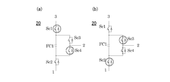
- the circuit diagram which shows the structure of a basic cell.
- FIG. It shows a power conversion device of the M phase 2 N + 1 +1 level in the third embodiment.
- FIG. The figure which shows the structural example of a phase module.
- the DC link capacitor is divided into two or less even at a level of 5 levels or more by connecting a plurality of basic cells composed of a common flying capacitor and a semiconductor device common to each phase to the DC link capacitor. Is.
- the charging / discharging of the flying capacitor can be performed freely according to the switching pattern, and multi-leveling of 9 levels or more can be realized without an external circuit.
- Embodiments 1 to 3 of the multilevel power conversion device according to the present invention will be described in detail with reference to FIGS.
- FIG. 1 A basic cell according to the first embodiment is shown in FIG. 1, and a switching pattern of the basic cell is shown in FIG.
- a circle in FIG. 2 indicates a semiconductor device (for example, IGBT) that is conducting.
- the basic cell of Embodiment 1 includes a flying capacitor FC1 and first to fourth semiconductor devices Sc1 to Sc4. This is the same cell as in Patent Document 1.
- the basic cell 20 includes a first semiconductor device Sc1 having one end connected to the third terminal 3, a second semiconductor device Sc2 having one end connected to the first terminal 1, the other end of the first semiconductor device Sc1, A flying capacitor FC1 connected between the other ends of the two semiconductor devices Sc2, a common connection point of the first semiconductor device Sc1 and the flying capacitor FC1, and a common connection point of the second semiconductor device Sc2 and the flying capacitor FC1. And third and fourth semiconductor devices Sc3 and Sc4 connected in series. The common connection point of the third and fourth semiconductor devices Sc3 and Sc4 becomes the second terminal 2.
- the switching pattern of the basic cell 20 is such that the first semiconductor device Sc1 and the fourth semiconductor device Sc4 are turned on as shown in FIG. 2A, or the second semiconductor device Sc2 and the third semiconductor device Sc4 are turned on as shown in FIG.
- the semiconductor device Sc3 is turned on.
- N stages of first to Nth common parts 11 to 1N are connected to the DC link capacitor DCC.
- J 1 (first common unit 11)
- 2 0 1 basic cells are connected.
- J 2 (second common unit 12)
- 2 1 2 basic cells
- J 3 (third common unit 13)
- the total number of the first to Nth common units 11 to 1N is 2 N ⁇ 1.
- the third terminal 3 is connected to the positive electrode of the DC link capacitor DCC, and the first terminal 1 is connected to the negative electrode of the DC link capacitor DCC.
- the basic cells of the second to Nth common parts 12 to 1N are connected in series by connecting the third terminal 3 and the first terminal 1 of the adjacent basic cells in each common part.
- the odd-numbered basic cells counted from the first terminal side of the basic cell 21a (that is, the negative electrode side of the DC link capacitor DCC) are connected to the second terminal 2 of the previous basic cell, and the third terminal 3 is connected.
- the first terminal 1 is connected to the first terminal 1 of the basic cell.
- the third terminal 3 is connected to the third terminal 3 of the preceding basic cell, and the first terminal 1 is connected to the second terminal 2 of the preceding basic cell. Is connected.
- the third terminal 3 of the first basic cell 22a counting from the first terminal 1 side of the basic cell 21a is connected to the first terminal 1 of the second basic cell 22b.
- the first basic cell 22a counted from the first terminal 1 side of the basic cell 21a has the third terminal 3 connected to the second terminal 2 of the basic cell 21a of the first common part 11, and the first common part 11
- the first terminal 1 is connected to the first terminal 1 of the basic cell 21a.
- the second basic cell 22b counted from the first terminal 1 side has the third terminal 3 connected to the third terminal 3 of the basic cell 21a of the first common part 11, and the second basic cell 22b of the basic cell 21a of the first common part 11 is connected.
- the first terminal 1 is connected to the two terminals 2.
- the basic cells of the third to Nth common units 13 to 1N are connected in the same manner.
- the DC voltage can be divided into 2 N +1 voltage levels by DCC.
- the input terminal of the phase module is connected to the first terminal 1, the second terminal 2, and the third terminal 3 of the basic cell of the Nth common unit 1N.
- the phase module is the same as in FIG.
- the configuration of the phase module shown in FIG. The first and second switching devices S1 and S2 are connected in series between the first input terminal I1 and the second input terminal I2.
- the third and fourth switching devices S3 and S4 are connected in series between the k-1 input terminal Ik-1 and the kth input terminal Ik.
- the fifth to eighth switching devices S5 to S8 are connected in series between the common connection point of the first and second switching devices S1 and S2 and the third input terminal I3.
- a capacitor FC1M is connected between the common connection point of the fifth and sixth switching devices S5 and S6 and the common connection point of the seventh and eighth switching devices S7 and S8.
- the ninth to twelfth switching devices S9 to S12 are connected in series between the k-2 input terminal Ik-2 and the common connection point of the third and fourth switching devices.
- a capacitor FCNM is connected between the common connection point of the ninth and tenth switching devices S9 and S10 and the common connection point of the eleventh and twelfth switching devices S11 and S12.
- the thirteenth to sixteenth switching devices S13 to S16 are connected in series between the common connection point of the sixth and seventh switching devices S6 and S7 and the common connection point of the tenth and eleventh switching devices S10 and S11.
- a capacitor FCMO is connected between the common connection point of the thirteenth and fourteenth switching devices S13 and S14 and the common connection point of the fifteenth and sixteenth switching devices S15 and S16.
- the common connection point of the fourteenth and fifteenth switching devices S14 and S15 is an output terminal.
- the first and second switching devices S1 and S2 are connected in series between the first input terminal I1 and the second input terminal I2.
- the third and fourth switching devices S3 and S4 are connected in series between the k-1 input terminal Ik-1 and the kth input terminal Ik.
- the fifth to tenth switching devices S5 to S10 are connected in series between the common connection point of the first and second switching devices S1 and S2 and the common connection point of the third and fourth switching devices S3 and S4.
- the first and second diodes D1 and D2 are connected in series between the common connection point of the fifth and sixth switching devices S5 and S6 and the common connection point of the seventh and eighth switching devices S7 and S8.
- a common connection point of the first and second diodes D1 and D2 is connected to the third input terminal I3.
- the third and fourth diodes D3 and D4 are connected in series between the common connection point of the seventh and eighth switching devices S7 and S8 and the common connection point of the ninth and tenth switching devices S9 and S10.
- a common connection point of the third and fourth diodes D3 and D4 is connected to the k-2 input terminal Ik-2.
- the eleventh and twelfth switching devices S11 and S12 are connected in series between the common connection point of the sixth and seventh switching devices S6 and S7 and the common connection point of the eighth and ninth switching devices S8 and S9.
- a common connection point of the eleventh and twelfth switching devices S11 and S12 is an output terminal.
- the first and second switching devices S1 and S2 are connected in series between the first input terminal I1 and the second input terminal I2.
- the third and fourth switching devices S3 and S4 are connected in series between the k-1 input terminal Ik-1 and the kth input terminal Ik.
- the fifth and sixth switching devices S5 and S6 are connected in reverse series to the third input terminal I3.
- the eighth and ninth switching devices S8 and S9 are connected in reverse series to the k-2 input terminal Ik-2.
- a seventh switching device S7 is connected between the common connection point of the first and second switching devices S1 and S2 and the sixth switching device S6.
- a tenth switching device S10 is connected between the common connection point of the third and fourth switching devices S3 and S4 and the ninth switching device S9.
- connection point of the sixth and seventh switching devices S6 and S7 and the common connection point of the ninth and tenth switching devices S9 and S10 are connected, and the connection point becomes an output terminal.
- the basic cell has two types of switching patterns shown in FIGS. 2 (a) and 2 (b). By selecting the pattern shown in FIGS. 2 (a) and 2 (b) according to the direction of one current, charging of the flying capacitor or The discharge can be arbitrarily selected.
- FIG. 4 is a diagram showing an M-phase 2 N +1 level multi-level conversion device including the DC link capacitor DCC, the first to Nth common units 11 to 1N, and the phase module shown in FIG.
- the multilevel power conversion device can output a phase voltage of 2 N +1 level.
- the thing of the structure of patent document 1 and FIG. 8 is used for a phase module.
- the number k of input terminals of the phase module of FIG. 8 is equal to the number of voltage levels 2 N +1.
- the number of divisions of the DC link capacitor DCC is set to 2 or less (1 in the first embodiment), and a multilevel power conversion device having a number of voltage levels exceeding five levels is provided. It becomes possible.
- the division number of the DC link capacitor DCC is 2 or less, the voltage balance of the divided DC link capacitor DCC can be easily obtained without connecting an external circuit. Thereby, it becomes possible to suppress that the harmonic component of the output phase voltage of the power converter increases due to the voltage balance being lost and adversely affects the load connected to the power converter.
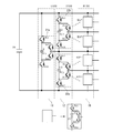
- FIG. 5 is a circuit diagram showing a multilevel power conversion device according to the second embodiment.
- a 9-level voltage can be output while the DC voltage is divided into two.
- the voltages of the DC link capacitors DCC1 and DCC2 are controlled to 4E.
- DC link capacitors DCC1, DCC2 are connected in series.
- a common connection point of the DC link capacitors DCC1 and DCC2 is defined as a neutral point NP.
- the first common unit 11 is provided with two basic cells 21a and 21b.
- the third terminal 3 of the basic cell 21a and the first terminal 1 of the basic cell 21b are connected.
- first terminal 1 of the basic cell 21a is connected to the negative terminal of the DC link capacitor DCC1
- third terminal 3 of the basic cell 21a is connected to the positive terminal of the DC link capacitor DCC1.
- the first terminal 1 of the basic cell 21b is connected to the negative terminal of the DC link capacitor DCC2, and the third terminal 3 of the basic cell 21b is connected to the positive terminal of the DC link capacitor DCC2.
- the second common unit 12 is provided with four basic cells 22a, 22b, 22c, and 22d.
- the third terminal 3 of the basic cell 22a and the first terminal 1 of the basic cell 22b are connected, the third terminal 3 of the basic cell 22b and the first terminal of the basic cell 22c are connected, and the third terminal 3 of the basic cell 22c
- the first terminal 1 of the basic cell 22d is connected.
- the first terminal 1 of the basic cell 22 a is connected to the first terminal 1 of the basic cell 21 a of the first common unit 11.
- the third terminal 3 of the basic cell 22 a is connected to the second terminal 2 of the basic cell 21 a of the first common unit 11.
- the first terminal 1 of the basic cell 22 b is connected to the second terminal 2 of the basic cell 21 a of the first common unit 11.
- the third terminal 3 of the basic cell 22 b is connected to the third terminal 3 of the basic cell 21 a of the first common unit 11.
- the first terminal 1 of the basic cell 22 c is connected to the first terminal 1 of the basic cell 21 b of the first common unit 11.
- the third terminal 3 of the basic cell 22 c is connected to the second terminal 2 of the basic cell 21 b of the first common unit 11.
- the first terminal 1 of the basic cell 22d is connected to the second terminal 2 of the basic cell 21b of the first common unit 11.
- the third terminal 3 of the basic cell 22 d is connected to the third terminal 3 of the basic cell 21 b of the first common unit 11.
- the input terminals of the three-phase phase modules 31, 32, and 33 are connected to the first terminal 1, the second terminal 2, and the third terminal 3 of the basic cells 22a to 22d of the second common unit 12 that is the final stage. .
- the phase module 31 will be described.
- the first and second switching devices S1u and S2u are connected in series between the third terminal 3 and the second terminal 2 of the basic cell 22d.
- Fifteenth and sixteenth switching devices S15u and S16u are connected in series between the second terminal 2 and the first terminal 1 of the basic cell 22a.
- the third and fourth switching devices S3u and S4u are connected in series between the common connection point of the first and second switching devices S1u and S2u and the first terminal 1 of the basic cell 22d.
- the thirteenth and fourteenth switching devices S13u and S14u are connected in series between the third terminal 3 of the basic cell 22a and the common connection point of the fifteenth and sixteenth switching devices S15u and S16u.
- the fifth and sixth switching devices S5u and S6u are connected in series between the common connection point of the third and fourth switching devices S3u and S4u and the second terminal 2 of the basic cell 22c.
- the eleventh and twelfth switching devices S11u and S12u are connected in series between the second terminal 2 of the basic cell 22b and the common connection point of the thirteenth and fourteenth switching devices S13u and S14u.
- the seventh to tenth switching devices S7u to S10u are connected in series between the common connection point of the fifth and sixth switching devices S5u and S6u and the common connection point of the eleventh and twelfth switching devices S11u and S12u.
- the first and second diodes D1u and D2u are connected in series between the common connection point of the seventh and eighth switching devices S7u and S8u and the common connection point of the ninth and tenth switching devices S9u and S10u.
- a common connection point of the first and second diodes D1u and D2u is connected to the neutral point NP.
- a common connection point of the eighth and ninth switching devices S8u and S9u is an output terminal.
- Table 1 shows the phase module switching patterns.
- the voltage level in Table 1 is the level of the output phase voltage of each phase with respect to the neutral point NP of the neutral point in FIG.
- one of the switching patterns of the basic cells 21a, 21b, 22a, 22b, 22c, and 22d constituting the first and second common units 11 and 12 is selected from (a) and (b) of FIG. It shall be.
- the potential of the input terminal of the phase module in FIG. 5 (that is, the output terminal of the second-stage basic cell) is as shown in FIG. 4E, 3E, 2E, E, 0, -E, -2E, -3E, and -4E. (Based on the potential of the NP terminal)
- FIG. 6 is a circuit diagram showing a multilevel power conversion device according to the third embodiment.
- the third embodiment is an M-phase 2 N + 1 +1 level multi-level power conversion device in which DC link capacitors DCC1 and DCC2 are connected in series in two stages.
- the first to Nth common units 11 to 11N have 2 ⁇ (2 1-1 ) to 2 ⁇ (2 N-1 ) basic cells, respectively. Since two DC link capacitors DCC1 and DCC2 are provided, the number of basic cells is 2 ⁇ (2 N ⁇ 1), which is twice that of 2 N ⁇ 1 in FIG. By using 2 ⁇ (2 N ⁇ 1) basic cells, it is possible to output a voltage of 2 N + 1 +1 level.
- the voltage of the DC link capacitors DCC1 and DCC2 is 4E, the Nth stage flying capacitor is divided into E / 2 N-1 voltage and controlled.
- the phase module uses the configuration shown in FIG. 8 as in Patent Document 1 and Embodiment 1. At this time, the number k of input terminals of the phase module in FIG. 8 is equal to the number of voltage levels (2 N + 1 +1).
- the first to third embodiments can be applied not only to a DC / AC converter that converts DC power into AC power but also to an AC / DC converter that converts AC power into DC power.
- an AC / DC converter When applied to an AC / DC converter, there is an effect that the harmonic current of the AC input power source connected to the DC / AC converter can be reduced.
Landscapes
- Engineering & Computer Science (AREA)
- Power Engineering (AREA)
- Inverter Devices (AREA)
Abstract
各相共通の直流リンクコンデンサDCCに各相共通の第1~第N共通部11~1N(N=2以上の整数)を接続する。第N共通部にM相(M=2以上の整数)の相モジュール31~3Mを接続する。第1~第N共通部11~1Nには、それぞれ21-1~2N-1個の基本セルが接続される。これにより、直流リンクコンデンサの分割数を2以下とし、5レベル以上の電圧レベル数のマルチレベル電力変換装置を提供する。
Description
本発明は、マルチレベル電力変換装置に係り、特に、各相共通の基本セルを用いた回路構成に関する。
図7は特許文献1の実施形態4に記載されている出力相電圧のレベル数が5以上となるマルチレベル電力変換装置の回路構成である。また、図8に、図7における相モジュールの構成例を示す。図8において、直流電圧群数P=2のときに、5レベル電力変換装置の相モジュールとなる。
例として、直流電圧群数P=2の回路での動作を説明する。直流リンクコンデンサDCC1、DCC2の電圧を2E、フライングキャパシタFC1,FC2の電圧をEに制御し、電力変換装置内の半導体デバイス(IGBTなど)を適正にオンオフ制御することによって、+2E,+E,0、-E、-2Eの5レベルの出力相電圧(出力端子OUT1,…,OUTMの相電圧)を生成する。なお、直流リンクコンデンサDCC1、DCC2の共通接続点を出力相電圧の基準点とする。
直流電圧群数Pが3以上の場合でも、同様の動作によって、2P+1レベルの出力相電圧を生成する
しかしながら、特許文献1の実施形態4を用いて5レベルより上の多レベル化を実現しようとする場合、直流電圧群数Pが3以上となり、直流リンクコンデンサ(DCC1,…,DCCP)を3つ以上直列に接続する必要がある。
しかしながら、特許文献1の実施形態4を用いて5レベルより上の多レベル化を実現しようとする場合、直流電圧群数Pが3以上となり、直流リンクコンデンサ(DCC1,…,DCCP)を3つ以上直列に接続する必要がある。
直流リンクコンデンサは2つまでであれば、非特許文献1に示すような制御方法で直流リンクコンデンサの電圧のバランスをとることが可能である。しかし、直流リンクコンデンサを3つ以上に分割すると、分割した直流リンクコンデンサの電圧のバランスを制御することが難しい。そのため、電圧を維持するために外部回路を接続しないと直流リンクコンデンサの電圧のバランスが取れないという問題があった。
これは回路の原理上生じる問題である。電圧指令値の大きさに応じて接続されるコンデンサ(直流リンクコンデンサDCC1,…DCCP、および、フライングキャパシタFC1,…,FCP)が異なるため、各コンデンサ、フライングキャパシタを使用する電力の大きさに異なりが生じ、電圧バランスが崩れてしまう。
電圧バランスが崩れることで、電力変換装置の出力相電圧の高調波成分が増加し、電力変換装置に接続する負荷へ悪影響を与えるという問題があった。
以上示したようなことから、直流リンクコンデンサの分割数を2以下とし、5レベル以上の電圧レベル数のマルチレベル電力変換装置を提供することが課題となる。
小笠原悟司,沢田直,赤木泰文,「中性点クランプ電圧形PWMインバータの中性点電位変動の解析」,電気学会論文誌D,113巻1号,平成5年
本発明は、前記従来の問題に鑑み、案出されたもので、その一態様は、各相共通の直流リンクコンデンサと、前記各相共通の直流リンクコンデンサに接続され、基本セルを有する各相共通の第1~第N共通部(N=2以上の整数)と、前記第N共通部に接続されたM相(M=2以上の整数)の相モジュールと、を備え、前記基本セルは、第3端子に一端が接続された第1半導体デバイスと、第1端子に一端が接続された第2半導体デバイスと、前記第1半導体デバイスの他端と前記第2半導体デバイスの他端との間に接続されたフライングキャパシタと、前記第1半導体デバイスと前記フライングキャパシタの共通接続点と前記第2半導体デバイスと前記フライングキャパシタの共通接続点との間に接続された第3,第4半導体デバイスと、を備え、前記第3,第4半導体デバイスの共通接続点を第2端子とし、前記第1共通部は、前記直流リンクコンデンサの正極端に前記第3端子が接続され、前記直流リンクコンデンサの負極端に前記第1端子が接続された1つの前記基本セルを有し、前記第2~第N共通部は、それぞれ前記基本セルを22-1~2N-1個有し、各共通部内の隣り合う前記基本セルの前記第3端子と前記第1端子とを接続して22-1~2N-1個の基本セルを直列接続し、前記第1共通部の基本セルの第1端子側から数えて奇数番目の前記基本セルは、前段の前記基本セルの前記第2端子に前記第3端子が接続され、前段の前記基本セルの前記第1端子に前記第1端子が接続され、前記第1共通部の基本セルの第1端子側から数えて偶数番目の前記基本セルは、前段の前記基本セルの前記第3端子に前記第3端子が接続され、前段の前記基本セルの前記第2端子に前記第1端子が接続され、前記相モジュールは、前記第N共通部の前記基本セルの前記第1~第3端子を入力端子とし、前記入力端子と出力端子との間にそれぞれスイッチングデバイスを有し、スイッチングデバイスを選択的にON,OFFすることにより、前記入力端子のうち何れかの端子の電位を選択して出力することを特徴とする。
また、他の態様として、各相共通の直流リンクコンデンサと、前記各相共通の直流リンクコンデンサに接続され、基本セルを有する各相共通の第1~第N共通部(N=2以上の整数)と、前記第N共通部に接続されたM相(M=2以上の整数)の相モジュールと、を備え、前記基本セルは、第3端子に一端が接続された第1半導体デバイスと、第1端子に一端が接続された第2半導体デバイスと、前記第1半導体デバイスの他端と前記第2半導体デバイスの他端との間に接続されたフライングキャパシタと、前記第1半導体デバイスと前記フライングキャパシタの共通接続点と前記第2半導体デバイスと前記フライングキャパシタの共通接続点との間に接続された第3,第4半導体デバイスと、を備え、前記第3,第4半導体デバイスの共通接続点を第2端子とし、前記第1共通部は、前記直流リンクコンデンサの正極端に前記第3端子が接続され、前記直流リンクコンデンサの負極端に前記第1端子が接続された1つの前記基本セルを有し、前記第2~第N共通部は、それぞれ前記基本セルを22-1~2N-1個有し、各共通部内の隣り合う前記基本セルの前記第3端子と前記第1端子とを接続して22-1~2N-1個の基本セルを直列接続し、前記第1共通部の基本セルの第1端子側から数えて奇数番目の前記基本セルは、前段の前記基本セルの前記第2端子に前記第3端子が接続され、前段の前記基本セルの前記第1端子に前記第1端子が接続され、前記第1共通部の基本セルの第1端子側から数えて偶数番目の前記基本セルは、前段の前記基本セルの前記第3端子に前記第3端子が接続され、前段の前記基本セルの前記第2端子に前記第1端子が接続され、前記相モジュールは、前記第N共通部の基本セルの前記第1~第3端子を入力端子とし、前記入力端子と出力端子との間にスイッチングデバイスとキャパシタを有し、前記スイッチングデバイスを選択的にON,OFFすることにより、前記入力端子のうち何れかの端子の電位、または、前記入力端子のうち何れかの端子の電位にキャパシタの電圧を加算または減算した電位を出力端子から出力することを特徴とする。
また、その一態様として、前記直流リンクコンデンサの電圧を2Eに制御し、第J共通部(J=1~Nまでの整数)の前記フライングキャパシタの電圧をE/2J-1に制御することを特徴とする。
また、他の態様として、各相共通の第1直流リンクコンデンサと、前記第1直流リンクコンデンサの正極端に負極端が接続された各相共通の第2直流リンクコンデンサと、前記各相共通の第1,第2直流リンクコンデンサに接続され、基本セルを有する各相共通の第1~第N共通部(N=2以上の整数)と、前記第N共通部に接続されたM相(M=2以上の整数)の相モジュールと、を備え、前記基本セルは、第3端子に一端が接続された第1半導体デバイスと、第1端子に一端が接続された第2半導体デバイスと、前記第1半導体デバイスの他端と前記第2半導体デバイスの他端との間に接続されたフライングキャパシタと、前記第1半導体デバイスと前記フライングキャパシタの共通接続点と前記第2半導体デバイスと前記フライングキャパシタの共通接続点との間に接続された第3,第4半導体デバイスと、を備え、前記第3,第4半導体デバイスの共通接続点を第2端子とし、前記第1共通部は、前記第1直流リンクコンデンサの正極端に前記第3端子が接続され、前記第1直流リンクコンデンサの負極端に前記第1端子が接続された第1の前記基本セルと、前記第2直流リンクコンデンサの正極端に前記第3端子が接続され、前記第2直流リンクコンデンサの負極端に前記第1端子が接続された第2の前記基本セルと、を有し、前記第2~第N共通部は、それぞれ前記基本セルを2×(22-1)~2×(2N-1)個有し、各共通部内の隣り合う前記基本セルの前記第3端子と前記第1端子とを接続して2×(22-1)~2×(2N-1)個の基本セルを直列接続し、前記第1共通部の第1の基本セルの第1端子側から数えて奇数番目の前記基本セルは、前段の前記基本セルの前記第2端子に前記第3端子が接続され、前段の前記基本セルの前記第1端子に前記第1端子が接続され、前記第1共通部の第1の基本セルの第1端子側から数えて偶数番目の前記基本セルは、前段の前記基本セルの前記第3端子に前記第3端子が接続され、前段の前記基本セルの前記第2端子に前記第1端子が接続され、前記相モジュールは、前記第N共通部の前記基本セルの前記第1~第3端子を入力端子とし、前記入力端子と出力端子との間にそれぞれスイッチングデバイスを有し、スイッチングデバイスを選択的にON,OFFすることにより、前記入力端子のうち何れかの端子の電位を選択して出力することを特徴とする。
また、他の態様として、各相共通の第1直流リンクコンデンサと、前記第1直流リンクコンデンサの正極端に負極端が接続された各相共通の第2直流リンクコンデンサと、前記各相共通の第1,第2直流リンクコンデンサに接続され、基本セルを有する各相共通の第1~第N共通部(N=2以上の整数)と、前記第N共通部に接続されたM相(M=2以上の整数)の相モジュールと、を備え、前記基本セルは、第3端子に一端が接続された第1半導体デバイスと、第1端子に一端が接続された第2半導体デバイスと、前記第1半導体デバイスの他端と前記第2半導体デバイスの他端との間に接続されたフライングキャパシタと、前記第1半導体デバイスと前記フライングキャパシタの共通接続点と前記第2半導体デバイスと前記フライングキャパシタの共通接続点との間に接続された第3,第4半導体デバイスと、を備え、前記第3,第4半導体デバイスの共通接続点を第2端子とし、前記第1共通部は、前記第1直流リンクコンデンサの正極端に前記第3端子が接続され、前記第1直流リンクコンデンサの負極端に前記第1端子が接続された第1の前記基本セルと、前記第2直流リンクコンデンサの正極端に前記第3端子が接続され、前記第2直流リンクコンデンサの負極端に前記第1端子が接続された第2の前記基本セルと、を有し、前記第2~第N共通部は、それぞれ前記基本セルを2×(22-1)~2×(2N-1)個有し、各共通部内の隣り合う前記基本セルの前記第3端子と前記第1端子とを接続して2×(22-1)~2×(2N-1)個の基本セルを直列接続し、前記第1共通部の第1の基本セルの第1端子側から数えて奇数番目の前記基本セルは、前段の前記基本セルの前記第2端子に前記第3端子が接続され、前段の前記基本セルの前記第1端子に前記第1端子が接続され、前記第1共通部の第1の基本セルの第1端子側から数えて偶数番目の前記基本セルは、前段の前記基本セルの前記第3端子に前記第3端子が接続され、前段の前記基本セルの前記第2端子に前記第1端子が接続され、前記相モジュールは、前記第N共通部の基本セルの前記第1~第3端子を入力端子とし、前記入力端子と出力端子との間にスイッチングデバイスとキャパシタを有し、前記スイッチングデバイスを選択的にON,OFFすることにより、前記入力端子のうち何れかの端子の電位、または、前記入力端子のうち何れかの端子の電位にキャパシタの電圧を加算または減算した電位を出力端子から出力することを特徴とする。
また、その一態様として、前記直流リンクコンデンサの電圧を4Eに制御し、第J共通部(J=1~Nまでの整数)の前記フライングキャパシタの電圧をE/2J-1に制御することを特徴とする。
本発明によれば、直流リンクコンデンサの分割数を2以下とし、5レベル以上の電圧レベル数のマルチレベル電力変換装置を提供することが可能となる。
本願は、直流リンクコンデンサに各相共通のフライングキャパシタと各相共通の半導体デバイスにより構成される基本セルを複数段接続することで、5レベル以上のレベルにおいても直流リンクコンデンサを2分割以下にするものである。
スイッチングパターンによりフライングキャパシタの充電・放電を自由に行うことが可能であり、9レベル以上の多レベル化を外部回路なしで実現できる。
以下、本願発明におけるマルチレベル電力変換装置の実施形態1~3を図1~図6に基づいて詳述する。
[実施形態1]
本実施形態1における基本セルを図1に示し、基本セルのスイッチングパターンを図2に示す。図2中の丸印は導通している半導体デバイス(例えば、IGBT)を示す。
本実施形態1における基本セルを図1に示し、基本セルのスイッチングパターンを図2に示す。図2中の丸印は導通している半導体デバイス(例えば、IGBT)を示す。
本実施形態1の基本セルはフライングキャパシタFC1と第1~第4半導体デバイスSc1~Sc4を備える。これは特許文献1と同一のセルである。
基本セル20は、第3端子3に一端が接続された第1半導体デバイスSc1と、第1端子1に一端が接続された第2半導体デバイスSc2と、第1半導体デバイスSc1の他端と、第2半導体デバイスSc2の他端との間に接続されたフライングキャパシタFC1と、第1半導体デバイスSc1とフライングキャパシタFC1の共通接続点と、第2半導体デバイスSc2とフライングキャパシタFC1の共通接続点と、の間に直列接続された第3,第4半導体デバイスSc3,Sc4と、を備えている。第3,第4半導体デバイスSc3,Sc4の共通接続点が第2端子2となる。
基本セル20のスイッチングパターンは、図2(a)に示すように第1半導体デバイスSc1と第4半導体デバイスSc4をON、または、図2(b)に示すように第2半導体デバイスSc2と第3半導体デバイスSc3をONする。
この基本セル20を用いた本実施形態1の共通部を図3に示す。本実施形態1は、直流リンクコンデンサDCCにN段の第1~第N共通部11~1N(N=2以上の整数)が接続される。
第J共通部1J(J=1~Nの整数)には、2J-1個の基本セルが接続される。例えば、J=1(第1共通部11)の場合、20=1個の基本セルが接続される。同様に、J=2(第2共通部12)の場合は21=2個の基本セルが、J=3(第3共通部13)の場合は22=4個の基本セルが、J=4(第4共通部14)の場合は23=8個の基本セルが接続される。第1~第N共通部11~1N合計で基本セルは2N-1個となる。
第1共通部11の基本セル21aは、直流リンクコンデンサDCCの正極に第3端子3が接続され、直流リンクコンデンサDCCの負極に第1端子1が接続される。
第2~第N共通部12~1Nの基本セルは、各共通部内の隣り合う基本セルの第3端子3と第1端子1とを接続して直列接続する。また、基本セル21aの第1端子側(すなわち、直流リンクコンデンサDCCの負極側)から数えて奇数番目の基本セルは、前段の基本セルの第2端子2に第3端子3が接続され、前段の基本セルの第1端子1に第1端子1が接続される。基本セル21aの第1端子側から数えて偶数番目の基本セルは、前段の基本セルの第3端子3に第3端子3が接続され、前段の基本セルの第2端子2に第1端子1が接続される。
ここで、例として第2共通部12の基本セル22a,22bについて説明する。基本セル21aの第1端子1側から数えて1番目の基本セル22aの第3端子3と2番目の基本セル22bの第1端子1とを接続する。また、基本セル21aの第1端子1側から数えて1番目の基本セル22aは、第1共通部11の基本セル21aの第2端子2に第3端子3が接続され、第1共通部11の基本セル21aの第1端子1に第1端子1が接続される。第1端子1側から数えて2番目の基本セル22bは、第1共通部11の基本セル21aの第3端子3に第3端子3が接続され、第1共通部11の基本セル21aの第2端子2に第1端子1が接続される。第3~第N共通部13~1Nの基本セルも同様に接続される。
図3に示すように、2N-1個の基本セル(N=1,2,3,…)を用いて第1~第N共通部11~1Nを接続することにより、1つの直流リンクコンデンサDCCで2N+1レベルの電圧レベルに直流電圧を分割することができる。
直流リンクコンデンサDCCの電圧を2Eとした時、第J共通部1J(J=1~Nの整数)のフライングキャパシタの電圧をE/2J-1に制御する。すなわち、第1共通部11のフライングキャパシタFC1の電圧をE,第2共通部12のフライングキャパシタFC2の電圧をE/2,…,第N共通部1NのフライングキャパシタFCの電圧をE/2N-1の電圧に分割し制御する。この分割した電圧レベルを選択する相モジュールをM相接続することでM相に拡張することが可能である。
第N共通部1Nの基本セルの第1端子1,第2端子2,第3端子3には、相モジュールの入力端子が接続される。相モジュールは図8と同様である。
図8(a)の相モジュールの構成を説明する。第1入力端子I1と第2入力端子I2との間に第1,第2スイッチングデバイスS1,S2が直列接続される。第k-1入力端子Ik-1と第k入力端子Ikとの間に第3,第4スイッチングデバイスS3,S4が直列接続される。
第1,第2スイッチングデバイスS1,S2の共通接続点と第3入力端子I3との間に第5~第8スイッチングデバイスS5~S8が直列接続される。第5,第6スイッチングデバイスS5,S6の共通接続点と第7,第8スイッチングデバイスS7,S8の共通接続点との間にキャパシタFC1Mが接続される。
第k-2入力端子Ik-2と第3,第4スイッチングデバイスの共通接続点との間に第9~第12スイッチングデバイスS9~S12が直列接続される。第9,第10スイッチングデバイスS9,S10の共通接続点と第11,第12スイッチングデバイスS11,S12の共通接続点との間にキャパシタFCNMが接続される。
第6,第7スイッチングデバイスS6,S7の共通接続点と第10,第11スイッチングデバイスS10,S11の共通接続点との間に第13~第16スイッチングデバイスS13~S16が直列接続される。第13,第14スイッチングデバイスS13,S14の共通接続点と第15,第16スイッチングデバイスS15,S16の共通接続点との間にキャパシタFCMOが接続される。また、第14,第15スイッチングデバイスS14,S15の共通接続点が出力端子となる。
次に、図8(b)の相モジュールの構成を説明する。第1入力端子I1と第2入力端子I2との間に第1,第2スイッチングデバイスS1,S2が直列接続される。第k-1入力端子Ik-1と第k入力端子Ikとの間に第3,第4スイッチングデバイスS3,S4が直列接続される。
第1,第2スイッチングデバイスS1,S2の共通接続点と第3,第4スイッチングデバイスS3,S4の共通接続点との間に第5~第10スイッチングデバイスS5~S10が直列接続される。
第5,第6スイッチングデバイスS5,S6の共通接続点と第7,第8スイッチングデバイスS7,S8の共通接続点との間に第1,第2ダイオードD1,D2が直列接続される。第1,第2ダイオードD1,D2の共通接続点は第3入力端子I3と接続される。第7,第8スイッチングデバイスS7,S8の共通接続点と第9,第10スイッチングデバイスS9,S10の共通接続点との間に第3,第4ダイオードD3,D4が直列接続される。第3,第4ダイオードD3,D4の共通接続点は第k-2入力端子Ik-2と接続される。
第6,第7スイッチングデバイスS6,S7の共通接続点と第8,第9スイッチングデバイスS8,S9の共通接続点との間に第11,第12スイッチングデバイスS11,S12が直列接続される。第11,第12スイッチングデバイスS11,S12の共通接続点が出力端子となる。
次に、図8(c)の相モジュールの構成を説明する。第1入力端子I1と第2入力端子I2との間に第1,第2スイッチングデバイスS1,S2が直列接続される。第k-1入力端子Ik-1と第k入力端子Ikとの間に第3,第4スイッチングデバイスS3,S4が直列接続される。
第3入力端子I3には、第5,第6スイッチングデバイスS5,S6が逆直列接続される。第k-2入力端子Ik-2には、第8,第9スイッチングデバイスS8,S9が逆直列接続される。
第1,第2スイッチングデバイスS1,S2の共通接続点と第6スイッチングデバイスS6との間には第7スイッチングデバイスS7が接続される。第3,第4スイッチングデバイスS3,S4の共通接続点と第9スイッチングデバイスS9との間には第10スイッチングデバイスS10が接続される。
第6,第7スイッチングデバイスS6,S7の共通接続点と第9,第10スイッチングデバイスS9,S10の共通接続点とが接続され、その接続点が出力端子となる。
相モジュールとして、図8(a)~(c)を説明したが、入力端子と出力端子との間にスイッチングデバイスを有し、入力端子の電位を選択して、または、入力端子の電位にキャパシタの電圧を加算・減算して出力するものであれば、他の構成でも良い。
基本セルには、図2(a)(b)の2種類のスイッチングパターンがあり、一つの電流の方向に応じて図2(a)(b)のパターンを選択することでフライングキャパシタの充電もしくは放電を任意に選択することができる。
したがって、充電・放電により電圧バランスをとることができるため、従来技術(図7)のように、直流リンクコンデンサDCCを多段に積むことなく、各フライングキャパシタで電圧を分担し、かつ、電圧バランスもとることが可能である。
図4は、図3に示す直流リンクコンデンサDCCおよび第1~第N共通部11~1Nと相モジュールから構成されるM相2N+1レベルのマルチレベル変換装置を示す図である。2N-1個の基本セルを用いてN段の第1~第N共通部11~1Nを多重接続することにより、マルチレベル電力変換装置は2N+1レベルの相電圧を出力することができる。
なお、相モジュールは、特許文献1や、図8の構成のものを使用する。この時、図8の相モジュールの入力端子数k=電圧レベル数2N+1となる。
以上示したように、本実施形態1によれば、直流リンクコンデンサDCCの分割数を2以下(本実施形態1では1)として、5レベルを超える電圧レベル数のマルチレベル電力変換装置を提供することが可能となる。
直流リンクコンデンサDCCの分割数が2以下であるため、外部回路を接続することなく、容易に分割した直流リンクコンデンサDCCの電圧バランスをとることができる。これにより、電圧バランスが崩れることで電力変換装置の出力相電圧の高調波成分が増加し、電力変換装置に接続する負荷へ悪影響を与えることを抑制することが可能となる。
[実施形態2]
図5は、本実施形態2におけるマルチレベル電力変換装置を示す回路図である。直流リンクコンデンサDCC1,DCC2を2段直列接続し、N=2,M=3とした場合の回路構成である。これにより直流電圧を2分割にしたままで、9レベルの電圧を出力することができる。なお、図5では、直流リンクコンデンサDCC1、DCC2の電圧を4Eに制御する。
図5は、本実施形態2におけるマルチレベル電力変換装置を示す回路図である。直流リンクコンデンサDCC1,DCC2を2段直列接続し、N=2,M=3とした場合の回路構成である。これにより直流電圧を2分割にしたままで、9レベルの電圧を出力することができる。なお、図5では、直流リンクコンデンサDCC1、DCC2の電圧を4Eに制御する。
本実施形態2におけるマルチレベル電力変換装置の具体的な構成を説明する。直流リンクコンデンサDCC1,DCC2が直列接続される。直流リンクコンデンサDCC1,DCC2の共通接続点を中性点NPとする。
第1共通部11には、2つの基本セル21a,21bが設けられる。基本セル21aの第3端子3と基本セル21bの第1端子1とが接続される。
また、基本セル21aの第1端子1は、直流リンクコンデンサDCC1の負極端に接続され、基本セル21aの第3端子3は、直流リンクコンデンサDCC1の正極端に接続される。基本セル21bの第1端子1は直流リンクコンデンサDCC2の負極端に接続され、基本セル21bの第3端子3は直流リンクコンデンサDCC2の正極端に接続される。
第2共通部12には、4つの基本セル22a,22b,22c,22dが設けられる。基本セル22aの第3端子3と基本セル22bの第1端子1が接続され、基本セル22bの第3端子3と基本セル22cの第1端子が接続され、基本セル22cの第3端子3と基本セル22dの第1端子1が接続される。
また、基本セル22aの第1端子1は第1共通部11の基本セル21aの第1端子1と接続される。基本セル22aの第3端子3は第1共通部11の基本セル21aの第2端子2と接続される。
基本セル22bの第1端子1は第1共通部11の基本セル21aの第2端子2と接続される。基本セル22bの第3端子3は第1共通部11の基本セル21aの第3端子3と接続される。
基本セル22cの第1端子1は第1共通部11の基本セル21bの第1端子1と接続される。基本セル22cの第3端子3は第1共通部11の基本セル21bの第2端子2と接続される。
基本セル22dの第1端子1は第1共通部11の基本セル21bの第2端子2と接続される。基本セル22dの第3端子3は第1共通部11の基本セル21bの第3端子3と接続される。
最終段である第2共通部12の基本セル22a~22dの第1端子1,第2端子2,第3端子3には、3相の相モジュール31,32,33の入力端子が接続される。
相モジュール31について説明する。基本セル22dの第3端子3と第2端子2との間に第1,第2スイッチングデバイスS1u,S2uが直列接続される。基本セル22aの第2端子2と第1端子1との間に第15,第16スイッチングデバイスS15u,S16uが直列接続される。
第1,第2スイッチングデバイスS1u,S2uの共通接続点と基本セル22dの第1端子1との間に第3,第4スイッチングデバイスS3u,S4uが直列接続される。基本セル22aの第3端子3と第15,第16スイッチングデバイスS15u,S16uの共通接続点との間に第13,第14スイッチングデバイスS13u,S14uが直列接続される。
第3,第4スイッチングデバイスS3u,S4uの共通接続点と基本セル22cの第2端子2の間に第5,第6スイッチングデバイスS5u,S6uが直列接続される。基本セル22bの第2端子2と第13,第14スイッチングデバイスS13u,S14uの共通接続点との間に第11,第12スイッチングデバイスS11u,S12uが直列接続される。
第5,第6スイッチングデバイスS5u,S6uの共通接続点と第11,第12スイッチングデバイスS11u,S12uの共通接続点との間に第7~第10スイッチングデバイスS7u~S10uが直列接続される。第7,第8スイッチングデバイスS7u,S8uの共通接続点と第9,第10スイッチングデバイスS9u,S10uの共通接続点との間に第1,第2ダイオードD1u,D2uが直列接続される。第1,第2ダイオードD1u,D2uの共通接続点は、中性点NPに接続される。第8,第9スイッチングデバイスS8u,S9uの共通接続点が出力端子となる。
相モジュールのスイッチングパターンを表1に示す。なお、表1の電圧レベルは、図5の中性点の中性点NPに対する各相の出力相電圧のレベルである。
この時、第1,第2共通部11,12を構成する各基本セル21a,21b,22a,22b,22c,22dのスイッチングパターンは図2の(a),(b)のいずれかが選択されているものとする。この各基本セル21a,21b,22a,22b,22c,22dの動作によって、図5の相モジュールの入力端子(すなわち、2段目の基本セルの出力端子)の電位は、図5の上から、4E,3E,2E,E,0,-E,-2E,-3E,-4Eとなる。(NP端子の電位を基準とする。)

以上示したように、本実施形態2によれば、直流電圧を2分割にしたままで、9レベルの電圧を出力することが可能となる。
[実施形態3]
図6は、本実施形態3におけるマルチレベル電力変換装置を示す回路図である。本実施形態3は、直流リンクコンデンサDCC1,DCC2を2段直列に接続したM相2N+1+1レベルのマルチレベル電力変換装置である。第1~第N共通部11~11Nは、それぞれ2×(21-1)~2×(2N-1)個の基本セルを有する。直流リンクコンデンサDCC1,DCC2を2つ設けているため、基本セルも図4の2N-1の2倍の2×(2N-1)個となる。2×(2N-1)個の基本セルを使用することで、2N+1+1レベルの電圧を出力することが可能となる。直流リンクコンデンサDCC1,DCC2の電圧を4Eとすると、N段目のフライングキャパシタはE/2N-1の電圧に分割し制御する。
図6は、本実施形態3におけるマルチレベル電力変換装置を示す回路図である。本実施形態3は、直流リンクコンデンサDCC1,DCC2を2段直列に接続したM相2N+1+1レベルのマルチレベル電力変換装置である。第1~第N共通部11~11Nは、それぞれ2×(21-1)~2×(2N-1)個の基本セルを有する。直流リンクコンデンサDCC1,DCC2を2つ設けているため、基本セルも図4の2N-1の2倍の2×(2N-1)個となる。2×(2N-1)個の基本セルを使用することで、2N+1+1レベルの電圧を出力することが可能となる。直流リンクコンデンサDCC1,DCC2の電圧を4Eとすると、N段目のフライングキャパシタはE/2N-1の電圧に分割し制御する。
なお、実施形態2は図6の回路においてN=2、M=3としたものである。なお、相モジュールは、特許文献1や実施形態1と同様、図8の構成を使用する。
この時、図8の相モジュールの入力端子数k=電圧レベル数(2N+1+1)となる。
この時、図8の相モジュールの入力端子数k=電圧レベル数(2N+1+1)となる。
なお、本実施形態1~3は、直流電力を交流電力に変換するDC/AC変換器だけではなく、交流電力を直流電力に変換するAC/DC変換器にも適用できる。AC/DC変換器に適用した場合は、DC/AC変換器に接続する交流入力電源の高調波電流を低減できる効果がある。
以上、本発明において、記載された具体例に対してのみ詳細に説明したが、本発明の技術思想の範囲で多彩な変形および修正が可能であることは、当業者にとって明白なことであり、このような変形および修正が特許請求の範囲に属することは当然のことである。
Claims (6)
- 各相共通の直流リンクコンデンサと、
前記各相共通の直流リンクコンデンサに接続され、基本セルを有する各相共通の第1~第N共通部(N=2以上の整数)と、
前記第N共通部に接続されたM相(M=2以上の整数)の相モジュールと、を備え、
前記基本セルは、第3端子に一端が接続された第1半導体デバイスと、第1端子に一端が接続された第2半導体デバイスと、前記第1半導体デバイスの他端と前記第2半導体デバイスの他端との間に接続されたフライングキャパシタと、前記第1半導体デバイスと前記フライングキャパシタの共通接続点と前記第2半導体デバイスと前記フライングキャパシタの共通接続点との間に接続された第3,第4半導体デバイスと、を備え、前記第3,第4半導体デバイスの共通接続点を第2端子とし、
前記第1共通部は、前記直流リンクコンデンサの正極端に前記第3端子が接続され、前記直流リンクコンデンサの負極端に前記第1端子が接続された1つの前記基本セルを有し、
前記第2~第N共通部は、それぞれ前記基本セルを22-1~2N-1個有し、各共通部内の隣り合う前記基本セルの前記第3端子と前記第1端子とを接続して22-1~2N-1個の基本セルを直列接続し、前記第1共通部の基本セルの第1端子側から数えて奇数番目の前記基本セルは、前段の前記基本セルの前記第2端子に前記第3端子が接続され、前段の前記基本セルの前記第1端子に前記第1端子が接続され、前記第1共通部の基本セルの第1端子側から数えて偶数番目の前記基本セルは、前段の前記基本セルの前記第3端子に前記第3端子が接続され、前段の前記基本セルの前記第2端子に前記第1端子が接続され、
前記相モジュールは、前記第N共通部の前記基本セルの前記第1~第3端子を入力端子とし、前記入力端子と出力端子との間にそれぞれスイッチングデバイスを有し、スイッチングデバイスを選択的にON,OFFすることにより、前記入力端子のうち何れかの端子の電位を選択して出力するマルチレベル電力変換装置。 - 各相共通の直流リンクコンデンサと、
前記各相共通の直流リンクコンデンサに接続され、基本セルを有する各相共通の第1~第N共通部(N=2以上の整数)と、
前記第N共通部に接続されたM相(M=2以上の整数)の相モジュールと、を備え、
前記基本セルは、第3端子に一端が接続された第1半導体デバイスと、第1端子に一端が接続された第2半導体デバイスと、前記第1半導体デバイスの他端と前記第2半導体デバイスの他端との間に接続されたフライングキャパシタと、前記第1半導体デバイスと前記フライングキャパシタの共通接続点と前記第2半導体デバイスと前記フライングキャパシタの共通接続点との間に接続された第3,第4半導体デバイスと、を備え、前記第3,第4半導体デバイスの共通接続点を第2端子とし、
前記第1共通部は、前記直流リンクコンデンサの正極端に前記第3端子が接続され、前記直流リンクコンデンサの負極端に前記第1端子が接続された1つの前記基本セルを有し、
前記第2~第N共通部は、それぞれ前記基本セルを22-1~2N-1個有し、各共通部内の隣り合う前記基本セルの前記第3端子と前記第1端子とを接続して22-1~2N-1個の基本セルを直列接続し、前記第1共通部の基本セルの第1端子側から数えて奇数番目の前記基本セルは、前段の前記基本セルの前記第2端子に前記第3端子が接続され、前段の前記基本セルの前記第1端子に前記第1端子が接続され、前記第1共通部の基本セルの第1端子側から数えて偶数番目の前記基本セルは、前段の前記基本セルの前記第3端子に前記第3端子が接続され、前段の前記基本セルの前記第2端子に前記第1端子が接続され、
前記相モジュールは、前記第N共通部の基本セルの前記第1~第3端子を入力端子とし、前記入力端子と出力端子との間にスイッチングデバイスとキャパシタを有し、前記スイッチングデバイスを選択的にON,OFFすることにより、前記入力端子のうち何れかの端子の電位、または、前記入力端子のうち何れかの端子の電位にキャパシタの電圧を加算または減算した電位を出力端子から出力するマルチレベル電力変換装置。 - 前記直流リンクコンデンサの電圧を2Eに制御し、
第J共通部(J=1~Nまでの整数)の前記フライングキャパシタの電圧をE/2J-1に制御する請求項1または2記載のマルチレベル電力変換装置。 - 各相共通の第1直流リンクコンデンサと、
前記第1直流リンクコンデンサの正極端に負極端が接続された各相共通の第2直流リンクコンデンサと、
前記各相共通の第1,第2直流リンクコンデンサに接続され、基本セルを有する各相共通の第1~第N共通部(N=2以上の整数)と、
前記第N共通部に接続されたM相(M=2以上の整数)の相モジュールと、を備え、
前記基本セルは、第3端子に一端が接続された第1半導体デバイスと、第1端子に一端が接続された第2半導体デバイスと、前記第1半導体デバイスの他端と前記第2半導体デバイスの他端との間に接続されたフライングキャパシタと、前記第1半導体デバイスと前記フライングキャパシタの共通接続点と前記第2半導体デバイスと前記フライングキャパシタの共通接続点との間に接続された第3,第4半導体デバイスと、を備え、前記第3,第4半導体デバイスの共通接続点を第2端子とし、
前記第1共通部は、前記第1直流リンクコンデンサの正極端に前記第3端子が接続され、前記第1直流リンクコンデンサの負極端に前記第1端子が接続された第1の前記基本セルと、前記第2直流リンクコンデンサの正極端に前記第3端子が接続され、前記第2直流リンクコンデンサの負極端に前記第1端子が接続された第2の前記基本セルと、を有し、
前記第2~第N共通部は、それぞれ前記基本セルを2×(22-1)~2×(2N-1)個有し、各共通部内の隣り合う前記基本セルの前記第3端子と前記第1端子とを接続して2×(22-1)~2×(2N-1)個の基本セルを直列接続し、前記第1共通部の第1の基本セルの第1端子側から数えて奇数番目の前記基本セルは、前段の前記基本セルの前記第2端子に前記第3端子が接続され、前段の前記基本セルの前記第1端子に前記第1端子が接続され、前記第1共通部の第1の基本セルの第1端子側から数えて偶数番目の前記基本セルは、前段の前記基本セルの前記第3端子に前記第3端子が接続され、前段の前記基本セルの前記第2端子に前記第1端子が接続され、
前記相モジュールは、前記第N共通部の前記基本セルの前記第1~第3端子を入力端子とし、前記入力端子と出力端子との間にそれぞれスイッチングデバイスを有し、スイッチングデバイスを選択的にON,OFFすることにより、前記入力端子のうち何れかの端子の電位を選択して出力するマルチレベル電力変換装置。 - 各相共通の第1直流リンクコンデンサと、
前記第1直流リンクコンデンサの正極端に負極端が接続された各相共通の第2直流リンクコンデンサと、
前記各相共通の第1,第2直流リンクコンデンサに接続され、基本セルを有する各相共通の第1~第N共通部(N=2以上の整数)と、
前記第N共通部に接続されたM相(M=2以上の整数)の相モジュールと、を備え、
前記基本セルは、第3端子に一端が接続された第1半導体デバイスと、第1端子に一端が接続された第2半導体デバイスと、前記第1半導体デバイスの他端と前記第2半導体デバイスの他端との間に接続されたフライングキャパシタと、前記第1半導体デバイスと前記フライングキャパシタの共通接続点と前記第2半導体デバイスと前記フライングキャパシタの共通接続点との間に接続された第3,第4半導体デバイスと、を備え、前記第3,第4半導体デバイスの共通接続点を第2端子とし、
前記第1共通部は、前記第1直流リンクコンデンサの正極端に前記第3端子が接続され、前記第1直流リンクコンデンサの負極端に前記第1端子が接続された第1の前記基本セルと、前記第2直流リンクコンデンサの正極端に前記第3端子が接続され、前記第2直流リンクコンデンサの負極端に前記第1端子が接続された第2の前記基本セルと、を有し、
前記第2~第N共通部は、それぞれ前記基本セルを2×(22-1)~2×(2N-1)個有し、各共通部内の隣り合う前記基本セルの前記第3端子と前記第1端子とを接続して2×(22-1)~2×(2N-1)個の基本セルを直列接続し、前記第1共通部の第1の基本セルの第1端子側から数えて奇数番目の前記基本セルは、前段の前記基本セルの前記第2端子に前記第3端子が接続され、前段の前記基本セルの前記第1端子に前記第1端子が接続され、前記第1共通部の第1の基本セルの第1端子側から数えて偶数番目の前記基本セルは、前段の前記基本セルの前記第3端子に前記第3端子が接続され、前段の前記基本セルの前記第2端子に前記第1端子が接続され、
前記相モジュールは、前記第N共通部の基本セルの前記第1~第3端子を入力端子とし、前記入力端子と出力端子との間にスイッチングデバイスとキャパシタを有し、前記スイッチングデバイスを選択的にON,OFFすることにより、前記入力端子のうち何れかの端子の電位、または、前記入力端子のうち何れかの端子の電位にキャパシタの電圧を加算または減算した電位を出力端子から出力するマルチレベル電力変換装置。 - 前記直流リンクコンデンサの電圧を4Eに制御し、
第J共通部(J=1~Nまでの整数)の前記フライングキャパシタの電圧をE/2J-1に制御する請求項4または5記載のマルチレベル電力変換装置。
Applications Claiming Priority (2)
| Application Number | Priority Date | Filing Date | Title |
|---|---|---|---|
| JP2017118203A JP6428859B1 (ja) | 2017-06-16 | 2017-06-16 | マルチレベル電力変換装置 |
| JP2017-118203 | 2017-06-16 |
Publications (1)
| Publication Number | Publication Date |
|---|---|
| WO2018230107A1 true WO2018230107A1 (ja) | 2018-12-20 |
Family
ID=64480497
Family Applications (1)
| Application Number | Title | Priority Date | Filing Date |
|---|---|---|---|
| PCT/JP2018/014179 Ceased WO2018230107A1 (ja) | 2017-06-16 | 2018-04-03 | マルチレベル電力変換装置 |
Country Status (2)
| Country | Link |
|---|---|
| JP (1) | JP6428859B1 (ja) |
| WO (1) | WO2018230107A1 (ja) |
Cited By (1)
| Publication number | Priority date | Publication date | Assignee | Title |
|---|---|---|---|---|
| JP2023513305A (ja) * | 2020-02-13 | 2023-03-30 | エスエムエイ ソーラー テクノロジー アクティエンゲゼルシャフト | 分割dcリンクを平衡化するための回路構成 |
Families Citing this family (1)
| Publication number | Priority date | Publication date | Assignee | Title |
|---|---|---|---|---|
| EP3913664A4 (en) | 2019-01-15 | 2023-02-01 | Cosmo Oil Lubricants Co., Ltd. | CURABLE COMPOSITION AND CURED MATERIAL |
Citations (3)
| Publication number | Priority date | Publication date | Assignee | Title |
|---|---|---|---|---|
| JP2010519890A (ja) * | 2007-02-21 | 2010-06-03 | アメリカン パワー コンバージョン コーポレイション | 三相で高電力の無停電電源 |
| WO2014208232A1 (ja) * | 2013-06-25 | 2014-12-31 | 株式会社明電舎 | マルチレベル電力変換装置 |
| JP2015047056A (ja) * | 2013-08-02 | 2015-03-12 | 株式会社明電舎 | マルチレベル電力変換装置 |
-
2017
- 2017-06-16 JP JP2017118203A patent/JP6428859B1/ja not_active Expired - Fee Related
-
2018
- 2018-04-03 WO PCT/JP2018/014179 patent/WO2018230107A1/ja not_active Ceased
Patent Citations (3)
| Publication number | Priority date | Publication date | Assignee | Title |
|---|---|---|---|---|
| JP2010519890A (ja) * | 2007-02-21 | 2010-06-03 | アメリカン パワー コンバージョン コーポレイション | 三相で高電力の無停電電源 |
| WO2014208232A1 (ja) * | 2013-06-25 | 2014-12-31 | 株式会社明電舎 | マルチレベル電力変換装置 |
| JP2015047056A (ja) * | 2013-08-02 | 2015-03-12 | 株式会社明電舎 | マルチレベル電力変換装置 |
Cited By (1)
| Publication number | Priority date | Publication date | Assignee | Title |
|---|---|---|---|---|
| JP2023513305A (ja) * | 2020-02-13 | 2023-03-30 | エスエムエイ ソーラー テクノロジー アクティエンゲゼルシャフト | 分割dcリンクを平衡化するための回路構成 |
Also Published As
| Publication number | Publication date |
|---|---|
| JP6428859B1 (ja) | 2018-11-28 |
| JP2019004626A (ja) | 2019-01-10 |
Similar Documents
| Publication | Publication Date | Title |
|---|---|---|
| US10447173B2 (en) | Single-phase five-level active clamping converter unit and converter | |
| US10044294B2 (en) | Apparatus and method for controlling asymmetric modular multilevel converter | |
| CN103314517B (zh) | 半导体电力变换装置 | |
| CN105453406B (zh) | 多电平电力变换装置 | |
| US9735664B2 (en) | Cascaded multi-level power converter | |
| JP5803683B2 (ja) | マルチレベル電力変換回路 | |
| CN103546052B (zh) | 多电平电压转换器 | |
| US20150365011A1 (en) | Bipolar double voltage cell and multilevel converter with such a cell | |
| US20180248493A1 (en) | Medium voltage transformerless multilevel converter and method for controlling a medium voltage transformerless multilevel converter | |
| US9917515B2 (en) | Cascadable modular 4-switch extended commutation cell | |
| US10389271B2 (en) | Single-phase four-level inverter circuit topology and three-phase four-level inverter circuit topology | |
| US9923369B2 (en) | Multilevel power convertor | |
| Saahithi et al. | Dual-topology cross-coupled configuration of switched capacitor converter for wide range of application | |
| Nilkar et al. | A new single-phase cascade multilevel inverter topology using four-level cells | |
| Hosseinpour et al. | A new symmetric/asymmetric multilevel inverter based on cascaded connection of sub-multilevel units aiming less switching components and total blocked voltage | |
| JP6428859B1 (ja) | マルチレベル電力変換装置 | |
| CN106160540A (zh) | 电力变换装置 | |
| JP2016208744A (ja) | マルチレベル電力変換器 | |
| WO2014162591A1 (ja) | 電力変換装置 | |
| JP2013078204A (ja) | 電力変換装置 | |
| US20150214830A1 (en) | System and method of power conversion | |
| JP2016158340A (ja) | 交流−交流変換装置 | |
| JP6131778B2 (ja) | 交流−交流変換装置 | |
| AU2012331406A1 (en) | Voltage converter having a first parallel circuit | |
| Kamani et al. | A new multilevel inverter topology with reduced device count and blocking voltage |
Legal Events
| Date | Code | Title | Description |
|---|---|---|---|
| 121 | Ep: the epo has been informed by wipo that ep was designated in this application |
Ref document number: 18817979 Country of ref document: EP Kind code of ref document: A1 |
|
| NENP | Non-entry into the national phase |
Ref country code: DE |
|
| 122 | Ep: pct application non-entry in european phase |
Ref document number: 18817979 Country of ref document: EP Kind code of ref document: A1 |