WO2018230022A1 - 送電器、受電器、送受電システム、自動取引装置および送受電方法 - Google Patents
送電器、受電器、送受電システム、自動取引装置および送受電方法 Download PDFInfo
- Publication number
- WO2018230022A1 WO2018230022A1 PCT/JP2018/000870 JP2018000870W WO2018230022A1 WO 2018230022 A1 WO2018230022 A1 WO 2018230022A1 JP 2018000870 W JP2018000870 W JP 2018000870W WO 2018230022 A1 WO2018230022 A1 WO 2018230022A1
- Authority
- WO
- WIPO (PCT)
- Prior art keywords
- power
- unit
- unmodulated
- main body
- banknote storage
- Prior art date
- Legal status (The legal status is an assumption and is not a legal conclusion. Google has not performed a legal analysis and makes no representation as to the accuracy of the status listed.)
- Ceased
Links
Images














Classifications
-
- G—PHYSICS
- G07—CHECKING-DEVICES
- G07D—HANDLING OF COINS OR VALUABLE PAPERS, e.g. TESTING, SORTING BY DENOMINATIONS, COUNTING, DISPENSING, CHANGING OR DEPOSITING
- G07D13/00—Handling of coins or of valuable papers, characterised by a combination of mechanisms not covered by a single one of groups G07D1/00 - G07D11/00
-
- G—PHYSICS
- G07—CHECKING-DEVICES
- G07D—HANDLING OF COINS OR VALUABLE PAPERS, e.g. TESTING, SORTING BY DENOMINATIONS, COUNTING, DISPENSING, CHANGING OR DEPOSITING
- G07D9/00—Counting coins; Handling of coins not provided for in the other groups of this subclass
-
- G—PHYSICS
- G07—CHECKING-DEVICES
- G07F—COIN-FREED OR LIKE APPARATUS
- G07F19/00—Complete banking systems; Coded card-freed arrangements adapted for dispensing or receiving monies or the like and posting such transactions to existing accounts, e.g. automatic teller machines
-
- H—ELECTRICITY
- H02—GENERATION; CONVERSION OR DISTRIBUTION OF ELECTRIC POWER
- H02J—ELECTRIC POWER NETWORKS; CIRCUIT ARRANGEMENTS OR SYSTEMS FOR SUPPLYING OR DISTRIBUTING ELECTRIC POWER; SYSTEMS FOR STORING ELECTRIC ENERGY
- H02J50/00—Circuit arrangements or systems for wireless supply or distribution of electric power
- H02J50/10—Circuit arrangements or systems for wireless supply or distribution of electric power using inductive coupling
- H02J50/12—Circuit arrangements or systems for wireless supply or distribution of electric power using inductive coupling of the resonant type
-
- H—ELECTRICITY
- H02—GENERATION; CONVERSION OR DISTRIBUTION OF ELECTRIC POWER
- H02J—ELECTRIC POWER NETWORKS; CIRCUIT ARRANGEMENTS OR SYSTEMS FOR SUPPLYING OR DISTRIBUTING ELECTRIC POWER; SYSTEMS FOR STORING ELECTRIC ENERGY
- H02J50/00—Circuit arrangements or systems for wireless supply or distribution of electric power
- H02J50/80—Circuit arrangements or systems for wireless supply or distribution of electric power involving the exchange of data, concerning supply or distribution of electric power, between transmitting devices and receiving devices
Definitions
- the present invention relates to a power transmitter, a power receiver, a power transmission / reception system, an automatic transaction apparatus, and a power transmission / reception method.
- the present invention claims the priority of Japanese Patent Application No. 2017-116127 filed on June 13, 2017, and for the designated countries where weaving by reference of documents is permitted, the contents described in the application are as follows: Is incorporated into this application by reference.
- Patent Document 1 is an automatic transaction apparatus that includes a main body housing and a bill storage that is provided so as to be able to be pulled out of the main body housing and stores a conveyed bill.
- a non-contact power transmission means and an apparatus-side wireless communication unit for performing information communication by electromagnetic waves are attached inside, and the banknote storage is a non-contact power reception means for receiving power from the non-contact power transmission means inside
- a storage-side wireless communication unit that is fed by the non-contact power receiving unit and performs information communication with the device-side wireless communication unit, and the non-contact power transmission unit and the non-contact power reception unit are the banknotes.
- the present invention provides a power-saving non-contact wireless between a power transmitter and a power receiver, and transmits power and information between the power transmitter and the power receiver at a reduced cost, a power receiver, a power transmission / reception system, and An object is to provide a power transmission / reception method.
- a power transmitter includes a control unit and a first non-contact power transmission unit including a first magnetic antenna that transmits non-contact first non-modulated power.
- a second magnetic antenna that receives the second unmodulated power transmitted in a contactless manner using a part of the first unmodulated power, and consumes the second unmodulated power.
- a non-contact power receiving unit including a first power receiving load, wherein the control unit changes a load state of the first power receiving load in accordance with a control content for controlling another device. The second unmodulated power is varied.
- FIG. 4 It is another example of the block diagram of the electric power supply part of the automatic transaction apparatus which concerns on 4th embodiment of this invention. It is an example of the figure which shows the structural example of the banknote storage of the automatic transaction apparatus which concerns on 4th embodiment of this invention. It is an example of the figure which shows the example of the waveform of the signal in case the drive electric power utilization part of the automatic transaction apparatus which concerns on 4th embodiment of this invention is a solenoid. It is an example of the figure which shows a structure at the time of adding a constant load part to the drive system of the automatic transaction apparatus which concerns on 4th embodiment of this invention. It is an example of the figure which shows a structure in case the drive electric power usage part of the automatic transaction apparatus which concerns on 4th embodiment of this invention is a DC motor.
- In-device wireless communication has advantages in that the number of connectors and harnesses between devices is reduced, so that the number of mounting steps can be reduced, the weight of an automatic transaction apparatus can be reduced, and maintenance and convenience can be improved.
- the banknote storage is often taken out of the main body of the automatic transaction apparatus for cash replenishment / collection, etc., but generally the banknote storage and the main body are connected by a connector.
- a publicly known example of this part is shown in, for example, Patent Document 1, and a device-side wireless communication unit for performing information communication with non-contact power transmission means and electromagnetic waves on the main body side is provided inside the banknote storage. It has a non-contact power receiving means and a storage-side wireless communication unit for performing information communication with the device-side wireless communication unit that is fed by the non-contact power receiving means.
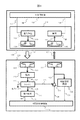
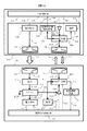
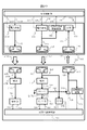
- FIG. 1 is an example of a block diagram of an automatic transaction apparatus according to a first embodiment of the present invention.
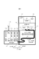
- FIG. 2 shows an example of a configuration diagram of a conventional automatic transaction apparatus.
- FIG. 3 the example of a block diagram of the automatic transaction apparatus which concerns on 1st embodiment of this invention is shown.
- FIG. 2 is an example of a configuration diagram of a conventional automatic transaction apparatus.
- the main body 100 of the automatic transaction apparatus includes a housing part 201 and a drawer part 202.
- the drawing unit 202 is shown in a state where it is pulled out from the housing unit 201 in FIG. 2, but is normally housed in the housing unit 201.
- the drawer unit 202 includes a plurality of banknote storage boxes 211.
- the drawer unit 202 includes five banknote storage boxes 211.
- subscripts such as 211a, 211b, 211c, 211d, 211e, respectively, and when writing the whole banknote storage, it describes with the banknote storage 211. .
- the casing unit 201 and the bill storage 211 are electrically connected by a plurality of connectors 212 provided on the main body side substrate 210 and a connector 213 in the bill storage 211. Wired connection.
- the connector 212 on the main body side substrate 210 and the connector 213 of the banknote storage 211 are detachable by inserting / removing corresponding uneven portions of a predetermined shape provided on both connectors.
- Various sensors and actuators such as solenoids and servo motors are incorporated in the banknote storage 211 and perform predetermined operations for storing and discharging banknotes.
- the plurality of connectors 212 of the main body side substrate 210 are connected to the control unit 207 and the power source / actuator unit 208 in the housing unit 201 via data wiring called power line 209 and power wiring.
- the plurality of connectors 212 of the main body side substrate 210 mediate power supply, actuator control in the bill storage 211, and exchange of information of various sensors.
- the actuator control in the bill storage 211 may be performed by creating a signal on the main body side substrate 210 from the power source and the actuator control information.
- a general operation of the automatic transaction apparatus main body 100 in a normal state in which the drawer unit 202 is housed in the housing unit 201 will be described below.
- the banknote is transported via the banknote transport path 206, the authenticity of the banknote and the denomination are discriminated by the identification unit 204, and the customer temporarily stores the banknote. It is temporarily suspended until payment is confirmed. Then, it distributes to each banknote storage 211a, 211b, 211c, 211d, 211e according to a money type via the banknote conveyance path 206.
- FIG. 3 is an example of a configuration diagram of the automatic transaction apparatus according to the first embodiment of the present invention.
- the connectors 212 and 213 shown in FIG. 2 are not used. Instead, the power transmission of the power source, the actuator control, and the information of various sensors are not used. Exchanges over the air. That is, in the automatic transaction apparatus according to the first embodiment of the present invention, the main body side substrate 210 is not provided with the connector 212, and the main body side wireless unit 102 is connected to the banknote storage 120 on the main body side substrate 210. One or a plurality are provided according to the number of entries.
- each banknote storage box 120a to 120e is provided with a wireless unit.
- FIG. 1 a main body side radio unit 102 on the main body side substrate 210 and one system configuration block for making the bill storage 120 wireless are shown.
- the main body side control unit 101 controls the main body side wireless unit 102 in addition to the control of the main body 100.
- the wireless power transmission from the main body side wireless unit 102 to the banknote storage 120 will be described.
- the main body control unit 101 outputs a clock 108 having a first carrier frequency for wireless power transmission to the power supply unit 103.
- the power supply unit 103 supplies the output power 110 according to the output power control signal 107 from the main body side control unit 101 to the main body side power transmission coil 104.
- the main body side power transmission coil 104 is connected to a capacitor so as to resonate at the first carrier frequency for wireless power transmission, thereby transmitting wireless power 121 by a magnetic field.
- the main body side power transmission coil 104 of FIG. 1 has shown the structure of series resonance, the structure of parallel resonance may be sufficient.
- the main body side power transmission coil 104 is not limited to a so-called coil with respect to its shape, material, etc., but may be any magnetic antenna that can transmit the wireless power 121 without modulation.
- the bill storage side receiving coil 112 is connected to a capacitor so as to resonate at the first carrier frequency for wireless power transmission, thereby receiving wireless power 121 by a magnetic field.
- the banknote storage side receiving coil 112 of FIG. 1 although the structure of series resonance is shown, the structure of parallel resonance may be sufficient.
- the banknote storage side receiving coil 112 is not limited to a so-called coil with respect to its shape, material, etc., but may be any magnetic antenna that can receive the wireless power 121 without modulation.
- the received power 123 received by the banknote storage side receiving coil 112 is rectified by the rectification unit 113 to become rectified power 124, becomes a stable direct current by the DC-DC conversion unit 114, and is supplied to each block.
- the banknote storage control unit 119 receives power supply and controls the power supplied to the power use unit 115 by the control signal 127.
- the power usage unit 115 is various sensors and actuators such as solenoids and servo motors.
- the power usage unit 115 performs an operation required in the banknote storage 120 upon receiving the supply of power 125 and outputs the obtained information 126 to the banknote storage control unit 119.
- a part 131 of the electric power obtained by the DC-DC converter 114 is supplied to the buffer 116.
- the buffer 116 buffers the clock 128 having the second carrier frequency output from the banknote storage controller 119 and supplies the output power 129 to the banknote storage side coil 117.
- the banknote storage side coil 117 is connected to a capacitor so as to resonate at a second carrier frequency for wireless power transmission, thereby transmitting wireless power 122 by a magnetic field.
- the banknote storage side coil 117 of FIG. 1 although the structure of series resonance is shown, the structure of parallel resonance may be sufficient.
- the banknote storage side coil 117 is not restricted to what is called a coil about the shape, material, etc., but should just be a magnetic antenna which can transmit the wireless electric power 122 without modulation
- the main body side coil 106 is connected to a capacitor so as to resonate at the second carrier frequency for wireless power transmission, and thereby receives the wireless power 122 by the magnetic field.
- the main body side coil 106 of FIG. 1 has shown the structure of series resonance, the structure of parallel resonance may be sufficient.
- the main body side coil 106 is not limited to a so-called coil with respect to its shape, material, etc., but may be any magnetic antenna that can receive the wireless power 122 without modulation.
- the power 111 received by the main body side coil 106 is consumed by the load 105.
- the control signal 109 is controlled in accordance with control information for controlling the banknote storage 120 from the main body 100, thereby controlling fluctuations in the wireless power 122.
- the fluctuation of the wireless power 122 is detected and demodulated by the control information demodulator 118 on the banknote storage side.
- a signal 130 obtained by detection and demodulation is control information for controlling the bill storage 120 from the main body 100.
- the control information demodulator 118 on the banknote storage side outputs this to the banknote storage controller 119, so that the banknote storage controller 119 can recognize control information for controlling the banknote storage 120 from the main body 100. .
- FIG. 4 is an example of a configuration diagram related to the control transmission operation of the automatic transaction apparatus according to the first embodiment of the present invention.
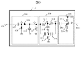
- FIG. 5 is a circuit diagram of a load according to the first embodiment of the present invention.
- FIG. 6 is a circuit diagram of the control information demodulator according to the first embodiment of the present invention.
- FIG. 7 is a diagram illustrating an example of a signal waveform of the automatic transaction apparatus according to the first embodiment of the present invention.
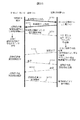
- a period 321 shown in FIG. 7 is a period in which control information for controlling the inside of the banknote storage 120 is not transmitted from the main body 100 to the banknote storage 120, and a period 322 is stored in the banknote storage 120 from the main body 100. This is a period during which control information for controlling the inside of the storage 120 is transmitted.
- the load 105 provided in the main body 100 includes, for example, resistors 301 and 303 and an NMOS-FET 302. ON / OFF of the NMOS-FET 302 is controlled by a control signal 109.
- High is ON and Low is OFF. Therefore, when the load 105 is OFF, only the resistor 303 is loaded.
- the load 105 is ON, if the ON resistance of the NMOS-FET 302 is ignored, the parallel of the resistors 301 and 303 becomes the load.
- the wireless power 122 shows a waveform shown in the period 321 in FIG. This is because the buffer 116 is supplied with a part 131 of the electric power obtained by the DC-DC converter 114, and the clock 128 of the second carrier frequency is buffered to output power 129, which is used as the banknote storage side coil 117. This corresponds to the non-modulated wireless power 122 that is supplied to and transmitted.
- the control signal 109 is changed to control information for controlling the banknote storage 120 from the main body 100.
- the control signal 109 is changed to High / Low.
- the load state of the load 105 is parallel to the resistors 301 and 303, and is smaller than that when the resistor 303 is used alone.
- reflected power (corresponding to the signal 130 obtained by detection and demodulation) is generated from the main body 100, and the wireless power 122 is combined with the reflected power, so that the amplitude changes. Therefore, the amplitude of the wireless power 122 changes according to the High / Low of the control signal 109.
- control information demodulation unit 118 includes a detection unit 304, a filter unit 305, and a voltage shift unit 306.
- the detection unit 304 detects an envelope that is a change in the amplitude of the wireless power 122 by the detection unit 304.
- the filter unit 305 removes frequency components equal to or higher than the second carrier frequency.
- the voltage shift unit 306 determines the threshold identification voltage of the demodulated signal, and outputs it as the detected and demodulated signal 130.
- the detection unit 304 includes a so-called voltage doubler detection circuit.
- the diode 308 is connected to the node 1 via the capacitor 307 with the received output power 129 via the capacitor 307 so as to be turned on from the GND to the node 1, and the diode 309 is connected in the direction from the node 1 to the node 2.
- the capacitor 310 is connected between the node 2 and GND, the resistor 311 is connected between the node 2 and GND, and the node 2 is used as an output.
- the filter unit 305 includes a so-called twin T notch filter circuit.
- the resistor 312 is connected between the input node and the node 3
- the resistor 313 is connected between the node 3 and the node 4
- the capacitor 314 is connected between the node 3 and GND.
- the capacitor 315 is connected between the input node and the node 5
- the capacitor 316 is connected between the node 5 and the node 4
- the resistor 317 is connected between the node 5 and the GND
- the node 4 is used as an output.
- the resistors 312 and 313 are approximately 6.8 k ⁇ (kiloohms)
- the resistor 317 is approximately 1.8 k ⁇
- the capacitors 314, 315, and 316 are approximately 10 pF ( Picofarad).
- the voltage shift unit 306, for example, divides the node 6 via the capacitor 318 between the voltage Vdd and the GND by the power obtained by the DC-DC conversion unit 114 by the resistor 319 and the resistor 320, and determines the threshold identification voltage. .
- the control signal 109 removes the DC voltage by Manchester encoding or other encoding methods.
- control information demodulator 118 obtains the detected and demodulated signal 130 as a signal obtained by inverting High / Low of the control signal 109.
- control information for controlling the inside of the banknote storage 120 is transmitted from the main body 100 to the banknote storage 120 with a simple configuration of changing the load state of the load 105 on the main body 100 side. Therefore, there is an effect that transmission of control information can be realized at low cost.
- the value of the load state of the load 105 can be set only with a simple condition that it is only necessary to transmit control information, there is an effect that it can be set to an optimum value even with low power.
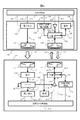
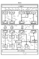
- FIG. 8 is an example of a block diagram of an automatic transaction apparatus according to a second embodiment of the present invention.
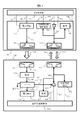
- the sensor information in the banknote storage 120 is transferred from the banknote storage 120 to the main body 100 between the main body side coil 106 and the banknote storage side coil 117.
- a configuration for transmitting banknote storage information is provided.
- FIG. 9 is an example of a block diagram relating to the operation of the switching unit that controls the bill storage of the automatic transaction apparatus according to the second embodiment of the present invention.
- the wireless power transmission mechanism from the main body side wireless unit 102 to the banknote storage 120 is the same as in FIG.
- the banknote storage side switching unit 413 according to the case where control information for controlling the inside of the banknote storage 120 is transmitted from the main body 100 to the banknote storage 120 between the banknote storage side coil 117 and the main body side coil 106.
- the operation of the switching unit 402 on the main body side is shown.
- the buffer 116 buffers the clock 128 of the second carrier frequency from the banknote storage controller 119, and outputs power. 129 is output to the switching unit 413.
- the switching unit 413 When receiving the control signal 411 from the banknote storage control unit 119, the switching unit 413 supplies the output power 129 to the banknote storage side coil 117 (transmission 415T) and connects to the control information demodulation unit 118 (transmission 416). .
- condenser is connected so that the banknote storage side coil 117 may resonate with the 2nd carrier wave frequency for wireless power transmission, and, thereby, transmits the wireless power 122 by a magnetic field.
- the main body side coil 106 is connected to a capacitor so as to resonate at the second carrier frequency for wireless power transmission, thereby receiving the wireless power 122 by the magnetic field.
- the received power 404 received is output to the switching unit 402.
- the switching unit 402 When the switching unit 402 receives the control signal 410 from the main body side control unit 101, the switching unit 402 connects the received power 404 to the load 105 (transmission 409), and the received power 404 is consumed by the load 105.
- the wireless power 122 By changing the load state using the control signal 109 from the main body side control unit 101, the wireless power 122 varies.
- the control signal 109 is controlled in accordance with control information for controlling the inside of the banknote storage 120 transmitted from the main body 100 to the banknote storage 120, thereby controlling fluctuations in the wireless power 122.
- This fluctuation of the wireless power 122 is detected and demodulated by the control information demodulator 118 on the banknote storage side.
- a signal 130 obtained by detection and demodulation is control information for controlling the bill storage 120 from the main body 100.
- the control information demodulator 118 on the banknote storage side outputs this to the banknote storage controller 119, so that the banknote storage controller 119 can recognize control information for controlling the banknote storage 120 from the main body 100. .
- the above mechanism is the same as the operation
- FIG. 10 is an example of a block diagram relating to the operation of the switching unit that transmits information to the main body of the automatic transaction apparatus according to the second embodiment of the present invention.
- the banknote storage side in the case of transmitting banknote storage information, such as sensor information in the banknote storage 120, from the banknote storage 120 to the main body 100 between the main body side coil 106 and the banknote storage side coil 117.
- the operations of the switching unit 413 and the switching unit 402 on the main body side are shown.
- the buffer 401 in the main body side radio unit 102 buffers the clock 407 of the second carrier frequency from the main body side control unit 101 and outputs the output power 408 to the switching unit 402.
- the switching unit 402 Upon receiving the control signal 410 from the main body side control unit 101, the switching unit 402 supplies output power 408 to the main body side coil 106 (transmission 404T) and connects to the banknote storage information demodulation unit 403 (transmission 405).
- the main body side coil 106 is connected to a capacitor so as to resonate at the second carrier frequency for wireless power transmission, thereby transmitting wireless power 414 by a magnetic field.
- the bill storage side coil 117 is connected to a capacitor so as to resonate at a second carrier frequency for wireless power transmission, and thereby receives wireless power 414 generated by a magnetic field.
- the received power 415 received is output to the switching unit 413.
- the switching unit 413 When the switching unit 413 receives the control signal 411 from the banknote storage control unit 119, the switching unit 413 connects the received power 415 to the load 412 (transmission 417), and the received power 415 is consumed by the load 412.
- the control signal 418 is controlled in accordance with banknote storage information such as sensor information in the banknote storage 120 transmitted from the banknote storage 120 to the main body 100, thereby controlling fluctuations in the wireless power 414. This fluctuation of the wireless power 414 is detected and demodulated by the bill storage information demodulator 403 on the main body side.
- a signal 406 obtained by being detected and demodulated is banknote storage information such as sensor information in the banknote storage 120 transmitted from the banknote storage 120 to the main body 100.
- the main body side control unit 101 can recognize banknote storage information such as sensor information in the banknote storage 120 transmitted from the banknote storage 120 to the main body 100.
- the direction of the wireless power between the main body side coil 106 and the banknote storage side coil 117 is reversed from the wireless power 122 to the wireless power 414 with respect to FIG.
- the operations of the load 412 and the load 105, the bill storage information demodulating unit 403, and the control information demodulating unit 118 are switched.
- the buffer 401 and the buffer 116, the load 412 and the load 105, the banknote storage information demodulator 403, and the control information demodulator 118 have the same circuit configuration.
- control information for controlling the inside of the banknote storage 120 can be transmitted from the main body 100 to the banknote storage 120 with a simple configuration of changing the load state on the main body 100 side.
- the banknote storage information such as sensor information in the banknote storage 120 can be transmitted from the banknote storage 120 to the main body with a simple configuration of changing the load state of the load 105 of the load 412 on the banknote storage 120 side. Therefore, there is an effect that transmission of control information and banknote storage information can be realized at low cost. Further, since the load state values of the load 105 and the load 412 can be set only under the condition that it is possible to transmit control information and banknote storage information, it can be set to an optimum value even with a small amount of power. effective.
- the buffer 116 or the buffer 401 is not selected by the switching unit 413 or the switching unit 402, respectively, the clock 128 or the clock 407 is stopped, or the power 131 of the buffer 116 or the buffer 401 is stopped.
- the operation of the buffer 116 or the buffer 401 may be stopped by stopping the supply of power.
- FIG. 11 is an example of a block diagram of an automatic transaction apparatus according to a third embodiment of the present invention.
- the control information for controlling the inside of the bill storage 120 from the main body 100 to the bill storage 120 between the bill storage side coil 117 and the main body side coil 106 as in FIG.
- the bill storage case information such as sensor information in the bill storage case 120 is transmitted from the bill storage case 120 to the main body 100.
- the third embodiment differs from the second embodiment in that a 3-state buffer 603 and a 3-state buffer 601 are used in place of the switching unit 413 and the buffer 116, and the switching unit 402 and the buffer 401, respectively. It is.
- the three-state buffer 603 is controlled by the control signal 410 and the control signal 411 so that the impedance becomes the output.
- the point different from FIG. 9 is that the bill storage information demodulator 403 is connected in FIG. If the input impedance of the bill storage information demodulating unit 403 is set to a high impedance that does not affect the load state value of the load 105, the fluctuation of the wireless power 122 due to the change in the load state is not affected.
- Control signals 411 and 410 are controlled so that 603 is high impedance and the 3-state buffer 601 is output.
- the difference from FIG. 10 is that the control information demodulator 118 is connected in FIG. If the input impedance of the control information demodulator 118 is set to a high impedance that does not affect the value of the load state of the load 412, it does not affect the fluctuation of the wireless power 414 due to the change of the load state.
- the operation similar to that of the second embodiment can be realized with a circuit configuration that is further simplified, so that control information and banknote storage information can be transmitted. There is an effect that can be realized at low cost.
- the banknote storage information demodulating unit 403 is always connected to the transmission 602 and the control information demodulating unit 118 is always connected to the transmission 604, the change of the load state of the load 105 is respectively changed to the banknote storage information demodulating unit 403.
- the change in the load state of the load 412 is echoed back as an operation confirmation signal to the main body side control unit 101 as a signal 406 and as a signal 130 to the banknote storage control unit 119 by the control information demodulation unit 118, respectively.
- the control information demodulation unit 118 There is an effect that can.
- FIG. 12 is an example of a block diagram of an automatic transaction apparatus according to a fourth embodiment of the present invention.
- control information for controlling the inside of the banknote storage 120 from the main body 100 to the banknote storage 120 using the banknote storage side coil 117 and the main body side coil 106.
- banknote storage information such as sensor information in the banknote storage 120 is transmitted from the banknote storage 120 to the main body 100.
- the power use unit 115 is divided into two systems, that is, a drive system power use unit 701 and a sensor system power use unit 702.
- the drive system power usage unit 701 operates an actuator system such as a solenoid, a DC motor, or a stepping motor.
- actuator systems generally have a higher drive voltage and higher drive current than the sensor system.
- 24V (volt) or 12V is used as the drive voltage
- the drive current is generally about 1A (ampere), for example.
- the sensor system requires that the input voltage be stabilized, but in the actuator system, there is often no problem in driving even if the drive voltage is not stabilized.
- the rectified power 124 that is the output of the rectification unit 113 can be directly supplied to the drive system power use unit 701.
- the drive system power use unit 701 is controlled to be turned on / off or forward / reversely driven by a control signal 705 from the banknote storage control unit 119, and in some cases, outputs an operation confirmation signal 704 to the banknote storage control unit 119. To do.
- the sensor system power usage unit 702 operates an optical sensor, for example, and generally operates at a voltage of about 5 V and consumes a current of at most 100 mA (milliampere) / piece, Often a regulated voltage is required. Accordingly, the sensor system power use unit 702 is supplied with power stabilized to the required voltage from the DC-DC conversion unit 114.
- the sensor system power usage unit 702 is given control information necessary for sensor operation by a control signal 707 from the banknote storage control unit 119, and outputs sensor information 706 obtained by the sensor to the banknote storage control unit 119.
- FIG. 13 is a diagram for explaining a problem of power supply of a general automatic transaction apparatus.
- a system that is wired and supplied with a drive voltage of 24 V for example, is divided into a power transmission system and a power reception system and wireless power is transmitted from the power transmission system to the power reception system.
- wireless power transmission it is necessary to temporarily convert to AC (AC) on the power transmission side, and it is necessary to rectify and convert the AC power to DC on the power receiving side.
- AC AC
- the transmission voltage is not adjusted at this time, it is generally 24V peak-to-peak alternating current, so even if full-wave rectification is performed by rectification, only a half voltage of 12V can be obtained on the power receiving side.
- the power receiving voltage on the power receiving side is smaller than 12V. Therefore, even if wireless power transmission is performed, it is necessary to boost the voltage in order to obtain the same power reception voltage as that of wired communication.
- boosting on the power transmission side and boosting on the power receiving side can be considered.
- each drive block such as the banknote storage control unit 119, [2] drive system power use unit 701 and [1], [3] sensor
- power usage situations such as the system power usage unit 702 and [1], [4] the drive system power usage unit 701 and the sensor system power usage unit 702 and [1]. Therefore, it is necessary to adjust the wireless power on the power transmission side according to each power usage situation.
- FIG. 13 shows an example in which 24V is converted to 48V and AC is doubled to 24V on the power receiving side.
- a method of adjusting the voltage on the power transmission side is shown in FIG.
- FIG. 14 is an example of a block diagram of the power supply unit of the automatic transaction apparatus according to the fourth embodiment of the present invention.
- FIG. 14 shows a configuration block in the case where the power supply amplifier 902 is a type in which the output gain is variable in accordance with the supplied power supply voltage. Specifically, the amplifier 902 has a class E amplifier configuration.
- the voltage of the power supply 903 is raised or lowered by the voltage adjustment unit 901 according to the output power control signal 107 from the main body side control unit 101 to obtain a supply voltage to the amplifier 902.
- the voltage adjustment unit 901 includes a step-up / step-down chopper, a step-up chopper, a step-down chopper, and the like, and the supply voltage value can be adjusted by changing the duty ratio of the output power control signal 107 as a PWM (Pulse Width Modulation) wave.
- the class E amplifier can be designed so that the peak-to-peak value of the output voltage is larger than the supply voltage.
- the class E amplifier is designed to supply the maximum value of the required voltage on the power receiving side, and the voltage adjustment unit 901 is a step-down chopper. It becomes possible to comprise. In addition, it is possible to design a class E amplifier so as to supply the minimum value of the required voltage on the power receiving side when the voltage of the power supply 903, and to configure the voltage adjustment unit 901 with a boost chopper.
- FIG. 15 is another example of a block diagram of the power supply unit of the automatic transaction apparatus according to the fourth embodiment of the present invention.
- FIG. 15 shows a configuration in which the power supply amplifier 905 can adjust the gain in accordance with the output power control signal 107. Specifically, this is a case where the amplifier 905 includes a voltage amplification unit and a buffer unit that can adjust the gain.
- the clock 108 having the first carrier frequency input to the amplifier 905 is output as an output power control signal.
- the voltage is amplified or attenuated in accordance with the gain adjustment of 107 and can be buffered from 0 V to the voltage boosted by the booster 904.
- the configuration block of the power supply unit 103 illustrated in FIGS. 14 and 15 can overcome the problem of voltage drop when the power supply is changed from wired to wireless shown in FIG. From [4] to [4], it is possible to cope with any of the power usage conditions on the power receiving side.
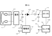
- FIG. 16 is an example of a diagram illustrating a configuration example of a banknote storage of the automatic transaction apparatus according to the fourth embodiment of the present invention. Specifically, this is a connection example of the rectification unit 113, the DC-DC conversion unit 114, the drive system power use unit 701, and the sensor system power use unit 702 of the bill storage 120 of the automatic transaction apparatus.
- the electric power received by the banknote storage side receiving coil 112 is rectified by the rectifying unit 113, smoothed by the capacitor 1001 connected to the GND, becomes electric power 1005, and is supplied to the drive system power using unit 701.
- the electric power 1005 further becomes electric power 1006 via the diode 1002.
- the diode 1002 is connected in a direction in which a current flows from the rectifier 113 to the DC-DC converter 114.
- the electric power 1006 becomes electric power 1007 through a filter including an inductor 1003 and a capacitor 1004 connected to GND, and is supplied to the DC-DC conversion unit 114.
- the DC-DC conversion unit 114 supplies power 1008 having a stabilized voltage required by the sensor system power usage unit 702 to the sensor system power usage unit 702.
- FIG. 17 is an example of a diagram illustrating an example of a signal waveform when the driving power usage unit of the automatic transaction apparatus according to the fourth embodiment of the present invention is a solenoid.
- the graph shown in FIG. 17A represents an output power control signal 107 for controlling the power supply unit 103 included in the main body 100 of the fourth embodiment shown in FIG.
- the horizontal axis is the time axis, and the vertical axis is the magnitude of the gain of the power supply unit 103.
- the period 1101 and the period 1104 are periods in which power is supplied to each drive block ([1]) such as the above-described [3] sensor system power usage unit 702 and banknote storage control unit 119.
- Periods 1102 and 1103 are periods in which power is supplied to each drive block ([1]) such as [4] drive system power use unit 701, sensor system power use unit 702, and bill storage control unit 119. .
- the period 1102 is a strong excitation period for starting up the solenoid
- the period 1103 is a weak excitation period for maintaining the solenoid.
- the waveform of FIG. 17B is taken.
- the electric power 1005 smoothed by the capacitor 1001 has an envelope waveform due to the rectification by the rectification unit 113 and the time constant due to the capacitance of the capacitor 1001, and the waveform of FIG.
- the solenoid In response to the control signal 705 from the banknote storage control unit 119, the solenoid is turned on during the periods 1102 and 1103, the solenoid operates, and a solenoid echo indicating the operation of the solenoid is output to the banknote storage control unit 119 as an operation confirmation signal 704. Is done.
- the electric power 1007 input to the DC-DC converter 114 has a waveform shown in FIG. 17C due to the effect of the filter constituted by the diode 1002, the inductor 1003, and the capacitor 1004. Due to the effect of the diode 1002, it is possible to prevent a backflow of current from the capacitor 1004 to the power 1005 side during a period when there is no power during the weak excitation period 1103 or during a steep rise during the strong excitation period 1102. Further, it is possible to avoid that the power 1007 falls below the input voltage required by the DC-DC converter 114. Further, when the diode 1002 is turned on by the inductor 1003, the capacities of the capacitors 1004 other than the capacitor 1001 cannot be seen in the capacitor capacities at the power 1005, and the envelope shown in FIG.
- the electric power 1007 does not drop below the input voltage required by the DC-DC converter 114 due to the effect of blocking the reverse current of the diode 1002. Therefore, the power 1008 that is the output of the DC-DC conversion unit 114 can be supplied to the sensor system power use unit 702 with the stabilized voltage required by the sensor system power use unit 702 shown in FIG.
- the second power is used between the first power usage system that uses large power or uses power intermittently and the second power usage system that requires stable power. Inserting a diode in a direction in which no current flows from the usage system to the first power usage system has an effect of stabilizing the input voltage of the second power usage system.
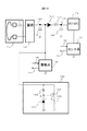
- FIG. 18 is an example of a diagram showing a configuration when a constant load unit is added to the drive system of the automatic transaction apparatus according to the fourth embodiment of the present invention.
- a constant load unit 1201 is further added to the connection example illustrated in FIG. 18 will be described with reference to FIGS. 19, 20, and 21.
- FIG. In this example, the drive system power usage unit 701 is a DC motor.
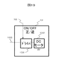
- FIG. 19 is an example of a diagram showing a configuration in the case where the driving power usage unit of the automatic transaction apparatus according to the fourth embodiment of the present invention is a DC motor. Electric power 1005 is supplied to the driver 1301, and the driver 1301 controls switching of rotation ON / OFF and normal / reverse rotation according to a control signal 705 from the banknote storage control unit 119 with respect to the connected DC motor 1302. Do.
- FIG. 20 is an output characteristic diagram of a general DC motor.
- the maximum torque is exhibited when the rotational load is large and the rotational speed is low, and the maximum current flows in that state.
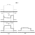
- FIG. 21 is a diagram showing an example of DC motor drive power of the automatic transaction apparatus according to the fourth embodiment of the present invention.
- FIG. 21A is a graph showing an output power control signal 107 for controlling the power supply unit 103 included in the main body 100 of the fourth embodiment.
- the horizontal axis is the time axis, and the vertical axis is the magnitude of the gain of the power supply unit 103.
- the period 1501 and the period 1503 are periods in which power is supplied to each drive block ([1]) such as the above-described [3] sensor system power usage unit 702 and banknote storage control unit 119.
- the period 1502 is a period during which power is supplied to each drive block ([1]) such as [4] drive system power use unit 701, sensor system power use unit 702, and bill storage control unit 119.
- the waveform of FIG. 21A is obtained at the power 1005 as the envelope of the received power.
- the DC motor 1302 is turned on during the period 1502, and the DC motor operates.
- the current waveform of the electric power 1005 at this time is shown in FIG. 21B, and the voltage waveform is shown in FIG. It is assumed that the DC motor 1302 is initially stopped, a rotation load is applied after the period 1504 from the start of rotation, and is stopped during the period 1505.
- the motor Immediately after the first motor ON control in the period 1502, the motor is stopped, and a rotational load having an appropriate static friction coefficient is applied, so that a large amount of current flows for a moment. Thereafter, when the motor starts to rotate, the rotational load decreases and the current decreases. In the period 1505, the maximum current flows because the motor is stopped by the rotational load.
- the constant load unit 1201 switches on when the voltage exceeds a certain voltage, releases the current, and keeps the load combined with the drive system power use unit 701 constant. Do not go higher than this.
- a specific circuit includes a resistor 1202 between the input contact of the driving system power use unit 701 and the node 1, and the node 1 and the GND so that a Zener voltage is generated at the node 1.
- a zener diode 1203 is provided between them.
- the source of the PMOS-FET 1204 is connected to the input node, the gate is connected to the node 1, the drain is connected to the node 2, and a resistor 1205 is provided between the node 2 and GND.
- FIG. 21D shows a voltage waveform of the electric power 1005 when the constant load unit 1201 is added. It can be said that the voltage rise is suppressed compared to the example of FIG.
- the driving system power use unit 701 is driven when the rotational load during rotation when the DC motor is used is light. There is an effect of suppressing an increase in input voltage of the system power use unit 701. At this time, the load of the constant load unit 1201 is adjusted so that the upper limit of the input voltage is the maximum power consumption used by the DC motor. In addition, it is possible to obtain an effect of suppressing a voltage increase on the power receiving side when power more than that required by the power receiving side is transmitted on the power transmitting side.
- FIG. 22 is a diagram showing an operation flow of the drive system power usage unit of the automatic transaction apparatus according to the fourth embodiment of the present invention.
- FIG. 22 shows an operation flow for operating the drive system power usage unit 701 shown in FIG. 17 or 21 in the configuration block of the automatic transaction apparatus of FIG.
- the control information demodulation unit 118 when information is transmitted from the main body 100 to the banknote storage 120, information is obtained by the control information demodulation unit 118 by changing the load state of the load 105 of the wireless power 122.
- the load state of the load 412 of the wireless power 414 is changed and information is obtained by the bill storage information demodulator 403.
- the main body side control unit 101 of the main body 100 instructs the operation start of the drive system power use unit 701 (step S1601).
- the banknote storage control unit 119 receives the operation start information and sets the operation of the drive system power usage unit 701 to ON by the control signal 705. After the setting, the banknote storage controller 119 transmits the preparation completion information to the main body 100 (step S1602).
- the main body side control unit 101 controls the power supply unit 103 by the output power control signal 107 to emit the wireless power for the drive system power use unit 701 (in the state [4] above) (step S1603).
- the banknote storage control part 119 observes the state in the banknote storage 120 with a sensor etc., and transmits the predetermined
- the banknote storage control unit 119 detects the completion of the operation of the drive system power usage unit 701 and requests the main body 100 to end the wireless power transmission operation (step S1605).
- the power supply part 103 changes from the state which emits the radio
- the storage controller 119 is notified (step S1606).
- the bill storage control unit 119 sets the operation of the drive system power use unit 701 to OFF by the control signal 705.
- FIG. 23 is a diagram showing an initial operation flow of the automatic transaction apparatus according to the fourth embodiment of the present invention.
- the main body side control unit 101 first emits wireless power 121 in order to confirm the presence of the banknote storage 120 on the main body 100 side (step S1701). .
- the power at this time is the power in the state [1], that is, the power for operating each drive block such as the banknote storage controller 119.
- the bill storage 120 receives the wireless power 121, and the DC-DC conversion unit 114 supplies power for the initial operation to the drive block to the bill storage control unit 119 and the like.
- the banknote storage control unit 119 is activated, and under the control of the banknote storage control unit 119, the 3-state buffer 603 is operated by a part of the received power 131, and the banknote storage side coil 117 is operated.
- the wireless power 122 is emitted (step S1702).
- the main body 100 side changes the three-state buffer 601 to a high impedance state by a control signal 410 from the main body side control unit 101, and the output of the banknote storage information demodulating unit 403 in order to confirm the reception of the wireless power 122.
- 406 is monitored by the main body control unit 101 (step S1703).
- the main body control unit 101 by changing the load state of the load 105 using the control signal 109 from the main body side control unit 101, whether or not the same echo back as the change appears in the output 406 of the banknote storage information demodulating unit 403 is determined. May be monitored from the main body side control unit 101.
- the main body side control unit 101 starts transmission of control information for controlling the banknote storage 120 to the banknote storage 120, and the banknote storage 120 receives the control information received. Then, a predetermined control operation is started.
- the main body side control unit 101 can confirm that the banknote storage 120 is normally present by checking the output of the wireless power 122 from the banknote storage 120.
- FIG. 24 is an example of a block diagram of an automatic transaction apparatus according to a fifth embodiment of the present invention.
- control information for controlling the inside of the banknote storage 120 is transmitted from the main body 100 to the banknote storage 120 between the banknote storage side coil 117 and the main body side coil 106.
- the bill storage case is transferred from the bill storage case 120 to the main body 100 between the main body side power transmission coil 104 and the bill storage case side power reception coil 112.
- the bill storage information such as sensor information in 120 is transmitted.
- the power received by the banknote storage side receiving coil 112 of the banknote storage 120 is directly supplied to the power usage unit 115 via the rectification unit 113 and the DC-DC conversion unit 114.
- the storage unit 1803 temporarily stores (charges) power, supplies power to each block from the storage unit 1803, supplies power 131 to the buffer 116, and supplies power to the power use unit 115.
- the wireless power supply from the main body side power transmission coil 104 to the banknote storage side power reception coil 112 can be uniformly sent in a predetermined amount.
- the control signal 1806 is associated with banknote storage information such as sensor information, whereby the banknote storage information can be transmitted from the banknote storage 120 to the main body 100 side.
- banknote storage information such as sensor information
- the operation described above is the same as that of FIG. 4 in which the main body 100 and the bill storage 120 are reversed in information transmission direction. That is, if the power receiving side load 105 is replaced with the load 1804 and the control information demodulating unit 118 is replaced with the banknote storage information demodulating unit 1801, the same mechanism can be said.
- the control information for controlling the inside of the bill storage 120 to be transmitted from the main body 100 to the bill storage 120 is between the bill storage side coil 117 and the main body side coil 106. Since banknote storage information such as sensor information in the banknote storage 120 transmitted from the banknote storage 120 to the main body 100 is transmitted between the main body side power transmission coil 104 and the banknote storage side power reception coil 112, control information is simultaneously transmitted. There is an effect that it is possible to exchange bill storage information. Further, since power is stored in the storage unit 1803, the wireless power 122 can be emitted from the banknote storage 120 to the main body 100 even when the wireless power 121 is not supplied. That is, there is an effect that control information for controlling the inside of the bill storage 120 can be transmitted from the main body 100 to the bill storage 120.
- FIG. 25 is an example of a block diagram of an automatic transaction apparatus according to the sixth embodiment of the present invention.
- the banknote storage 120 has the storage unit 1803.
- the power supply type supplies power from the DC-DC converter 114 to the buffer 116.
- each drive block such as the banknote storage control unit 119 described above. Or when power is supplied to [3] sensor system power usage unit 702 and [1].
- power supply to the above [2] drive system power usage unit 701 and [1] or [4 It can be realized even when power is supplied to the drive system power use unit 701, the sensor system power use unit 702, and [1].
- FIG. 26 is an example of a block diagram of an automatic transaction apparatus according to a seventh embodiment of the present invention.
- the clock 128 of the second carrier frequency that is input to the buffer 116 or the three-state buffer 603 is obtained from the bill storage controller 119.
- the frequency divider 2001 divides the frequency of the first carrier wave frequency component included in the power 1805 of the wireless power 121 received by the banknote storage side receiving coil 112.
- the clock 2002 is the second carrier frequency.
- the frequency divider 2001 divides the frequency by, for example, 1/2 to set a frequency half the first carrier frequency as the second carrier frequency.
- FIG. 26 shows an example in which the present embodiment is applied to the sixth embodiment, but the present embodiment is not limited to this, and it is obvious that the present embodiment can be applied to other embodiments.
- the seventh embodiment shown in FIG. 26 since it is not necessary to oscillate the second carrier frequency in the banknote storage controller 119, not only the processing of the banknote storage controller 119 is reduced, There is an effect that the cost can be reduced.
- the first carrier frequency and the second carrier frequency are synchronized.
- the second carrier frequency is a frequency division of the first carrier frequency
- the second carrier frequency is the first carrier frequency. The frequency is lower than the carrier frequency. Therefore, there is an effect that there is no harmonic interference from the wireless power 121 that is the first carrier frequency to the wireless power 122 that is the second carrier frequency.
- FIG. 27 is an example of a block diagram of an automatic transaction apparatus according to an eighth embodiment of the present invention.
- the power supply to the drive system power use unit 701 and the sensor system power use unit 702 is the same as that of the main body side power transmission coil 104.
- the main body side power transmission coil 2102 is provided in the main body 100 independently for the drive system power use unit 701.
- the banknote storage 120 side receiving coil 2107 is provided in the banknote storage 120, and the wireless power 2106 is transmitted independently for the drive system power usage unit 701.
- the main body side control unit 101 outputs a clock 2104 having a third carrier frequency for wireless power transmission to the power supply unit 2101.
- the power supply unit 2101 supplies output power 2105 according to the output power control signal 2103 from the main body side control unit 101 to the main body side power transmission coil 2102.
- the main body side power transmission coil 2102 is connected to a capacitor so as to resonate at the third carrier frequency for wireless power transmission, thereby transmitting the wireless power 2106 by the magnetic field.
- the main body side power transmission coil 2102 in FIG. 27 shows a configuration of series resonance, a configuration of parallel resonance may be used.
- the main body side power transmission coil 2102 is not limited to a so-called coil in terms of its shape, material, etc., but may be any magnetic antenna that can transmit wireless power 2106 without modulation.
- the bill storage side receiving coil 2107 is connected to a capacitor so as to resonate at a third carrier frequency for wireless power transmission, and thereby receives wireless power 2106 by a magnetic field.
- the banknote storage side receiving coil 2107 of FIG. 27 although the structure of series resonance is shown, the structure of parallel resonance may be sufficient.
- the bill storage case-side receiving coil 2107 is not limited to a so-called coil with respect to its shape, material, etc., but may be any magnetic antenna that can receive wireless power 2106 without modulation. .
- the power 2109 received by the banknote storage side power receiving coil 2107 is rectified by the rectification unit 2108 to become rectified power 2110, and is supplied to the drive system power usage unit 701.
- the banknote storage control unit 119 receives power supply and controls the drive system power use unit 701 by a control signal 705.
- the drive system power usage unit 701 is an actuator such as a solenoid or a servo motor.
- the drive system power usage unit 701 performs an operation required in the banknote storage 120 upon receiving the supply of power 2110, and outputs the obtained operation confirmation signal 704 to the banknote storage control unit 119.
- banknote storage such as sensor information in the banknote storage 120 from the banknote storage 120 to the main body 100 between the main body side power transmission coil 104 and the banknote storage side power reception coil 112.
- the drive system power use unit 701. Power is supplied via a separate system, so that the wireless power supply is uniformly supplied from the main body side power transmission coil 104 to the bill storage case side power reception coil 112 regardless of the operation period of the drive system power usage unit 701.
- banknote storage information such as sensor information in the banknote storage 120 can be transmitted from the banknote storage 120 to the main body 100 during There is a similar effect.
- FIG. 28 is an example of a block diagram of an automatic transaction apparatus according to the ninth embodiment of the present invention.
- the drive system power usage unit 701 of the eighth embodiment shown in FIG. 27 there are a plurality of actuators such as solenoids and servo motors, and the ON / OFF and control of each operation is performed from the bill storage control unit 119. It was controlled by the control signal 705.
- the power supply unit 2101, the main body side power transmission coil 2102, the banknote storage side power reception coil 2107, and the rectification unit 2108 of FIG. 27 are separately prepared for each of the plurality of actuators.
- FIG. 28 shows an example in which there are two systems of actuators, and the difference between the systems is represented by the suffixes a and b.
- the drive system power use unit 701 is separated into individual drive system power use units 2201a and 2201b according to a plurality of systems.
- the solenoid or DC motor has a constant rotation direction, it is possible to control the drive ON / OFF according to whether power is supplied or not.
- the inside of the bill storage 120 is controlled from the main body 100 that transmits between the bill storage side coil 117 and the main body side coil 106 using the wireless power 122 to the bill storage case 120.
- ON / OFF control of the drive system power use unit 2201a and the drive system power use unit 2201b by controlling the wireless transmission of the power 2106a and the power 2106b independently from the main body 100 to the bill storage 120 without the exchange of control information. There is an effect that can be performed.
- FIG. 29 is an example of a configuration diagram of an automatic transaction apparatus according to a tenth embodiment of the present invention.
- the bill storage 120 can be connected to a terminal 2301 other than the main body 100 and handled.
- the banknote storage 120 is taken out from the main body 100, and the banknotes in the banknote storage 120 are replenished or taken out at another place while being connected to the terminal 2301.
- FIG. 30 shows a configuration block diagram of the automatic transaction apparatus corresponding to this
- FIG. 31 shows an operation description of the configuration block of the terminal 2301 and the bill storage 120.
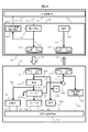
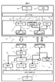
- FIG. 30 is an example of a block diagram of an automatic transaction apparatus according to the tenth embodiment of the present invention. 30 is different from the fourth embodiment shown in FIG. 12 in that a main body side memory 2401 connected to the main body side control unit 101 and capable of reading and writing from the main body side control unit 101 is provided in the main body 100.
- the banknote storage 120 is connected to the banknote storage control unit 119, and the banknote storage side memory 2402 that can be read and written from the banknote storage control unit 119 is provided.
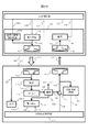
- FIG. 31 is an example of a block diagram of a power transmission / reception system according to the tenth embodiment of the present invention.
- a terminal 2301 basically includes the same configuration blocks as those of the main body 100, and is connected to a terminal-side radio unit 102T and a terminal-side control unit 2502 to be connected to the terminal-side radio unit 102T and the terminal-side control unit.
- 2502 a terminal-side memory 2501 that can be read and written, and a terminal-side control unit 2502, are connected to an external device, a mobile phone network, the Internet, a LAN (Local Area Network), a WAN (Wide Area Network), etc.
- the communication unit 2503 communicates via a communication network regardless of the various types of wired and wireless communication.
- the memory 2501 may be detachably attached to the terminal 2301.
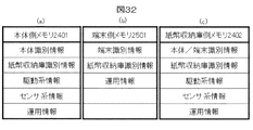
- FIG. 32 shows the contents stored in each memory.
- FIG. 32 is an example of a diagram showing a data structure used in the power transmission / reception system according to the tenth embodiment of the present invention.
- main body identification information including information indicating the main body, information on the main body model name, version, serial number, and the like, and the model name and version of the bill storage that can be stored in the main body 100
- Banknote identification information that can identify a serial number
- drive system information including control information of an actuator used in the drive system power use unit 701
- Sensor system information including information, etc., operational information regarding the installation location of the automatic transaction apparatus and the number of banknotes deposited in the banknote storage 120 are stored.
- the memory 2501 on the terminal side includes terminal identification information including information indicating the terminal, information indicating available authority, and the like, and a banknote storage including the model name and version of the banknote storage that can be controlled by the terminal 2301
- terminal identification information including information indicating the terminal, information indicating available authority, and the like
- banknote storage including the model name and version of the banknote storage that can be controlled by the terminal 2301
- the identification information and the above-described operation information are stored.
- the memory 2402 on the banknote storage side identifies the main body and the terminal, and in the case of a terminal, the main body / terminal identification information that can identify the authority, the above-described banknote storage identification information, drive system information, Sensor system information and operation information are stored.
- main body identification information, the terminal identification information, and the main body / terminal identification information are not normally rewritten except for special operation situations such as software update.
- the drive system information, the sensor system information, and the operation information are rewritten by control from the main body side control unit 101 of the main body 100 or training or sensor information by the banknote storage control unit 119 in the banknote storage 120.
- the main body 100 and the bill storage 120 are always synchronized so as to have the same information.
- FIG. 33 is a diagram showing an initial operation flow of the power transmission / reception system according to the tenth embodiment of the present invention.
- FIG. 33 shows an operation flow of an initial operation of the automatic transaction apparatus according to the tenth embodiment shown in FIGS. 30 and 31.
- the main body side control unit 101 (or terminal side control unit 2502) emits wireless power 121 (step S1701).
- the power at this time is the power in the state [1], that is, the power for operating each drive block such as the banknote storage controller 119.
- the bill storage 120 receives the wireless power 121, and the DC-DC conversion unit 114 supplies power for the initial operation to the drive block to the bill storage control unit 119 and the like.
- the banknote storage control unit 119 is activated, and under the control of the banknote storage control unit 119, the 3-state buffer 603 is operated by a part of the received power 131, and the banknote storage side coil 117 is operated.
- the wireless power 122 is emitted (step S1702).
- the main body side control unit 101 of the main body 100 (or the terminal side control unit 2502 of the terminal 2301) transmits the main body identification information (or terminal identification information) to the banknote storage 120 (step S2701).
- the banknote storage control part 119 of the banknote storage 120 recognizes whether the other party who has transmitted information is the main body 100 or the terminal 2301. If it cannot be recognized, or if it is an inappropriate individual, it is determined that it is not a proper main body or terminal, and the transmission of the wireless power 122 is stopped. In the case of the terminal 2301, the banknote storage control unit 119 further confirms the authority given to the terminal 2301. For example, it has the authority to open the door of the banknote storage 120 and take out banknotes, or the authority to take out banknotes but obtain operational information, etc. is there. When these confirmations are completed, the banknote storage control unit 119 transmits confirmation completion information to the main body 100 (step S2702).
- the main body side control unit 101 of the main body 100 requests the banknote storage 120 to transmit banknote storage identification information (step S2703).
- the banknote storage control unit 119 transmits the banknote storage identification information to the main body 100 (or the terminal 2301) (step S2704). Thereafter, the main body side control unit 101 of the main body 100 (or the terminal side control unit 2502 of the terminal 2301) confirms the transmitted banknote storage identification information, and starts control of the banknote storage 120 if there is no problem.
- the terminal 2301 After performing the initial processing in this way, the terminal 2301 obtains operation information from the bill storage 120, writes it in the memory 2501, and transmits the operation information to an external device or the like via the communication unit 2503 in some cases. Moreover, when using the terminal 2301 with a legitimate authority, the banknote storage controller 119 controls the banknote storage 120 so that the banknote storage 120 can be opened and the banknotes can be taken out.
- identification is performed between the main body 100 or the terminal 2301 and the banknote storage 120. Since identification processing using information is performed, there is an effect that information transmission with high security can be achieved.
- elements specific to the embodiment are added based on the fourth embodiment shown in FIG. 12, but elements specific to the embodiment are added based on other examples. Obviously it can be added.
- each of the above-described configurations, functions, processing units, and the like may be realized by hardware by designing a part or all of them with, for example, an integrated circuit.
- Each of the above-described configurations, functions, and the like may be realized by software by interpreting and executing a program that realizes each function by the processor.
- Information such as programs, tables, and files that realize each function can be stored in a recording device such as a memory or a hard disk, or a recording medium such as an IC card, an SD card, or a DVD.
- control lines and information lines are those that are considered necessary for the explanation, and not all control lines and information lines on the product are necessarily shown. Actually, it may be considered that almost all the components are connected to each other. In the above, this invention was demonstrated centering on embodiment.
- SYMBOLS 100 ... Main body, 101 ... Main body side control part, 102 ... Main body side radio
Landscapes
- Engineering & Computer Science (AREA)
- Computer Networks & Wireless Communication (AREA)
- Power Engineering (AREA)
- Physics & Mathematics (AREA)
- General Physics & Mathematics (AREA)
- Business, Economics & Management (AREA)
- Accounting & Taxation (AREA)
- Finance (AREA)
- Financial Or Insurance-Related Operations Such As Payment And Settlement (AREA)
- Near-Field Transmission Systems (AREA)
Abstract
送電器と受電器の間を省配線非接触無線化とすると共に、コストを抑えて電力及び情報を送電器と受電器の間で伝送する。 制御部と、非接触で第1の無変調の電力を送電する第1の磁気アンテナを備えた第1の非接触送電部と、第1の無変調の電力の一部を用いて非接触で送電された第2の無変調の電力を受電する第2の磁気アンテナと、第2の無変調の電力を消費する第1の受電負荷と、を備える非接触受電部と、を備え、制御部は、第1の受電負荷の負荷状態を、他の装置を制御する制御内容に対応して変化させることで第2の無変調の電力を変動させる、ことを特徴とする送電器。
Description
本発明は送電器、受電器、送受電システム、自動取引装置および送受電方法に関する。本発明は2017年6月13日に出願された日本国特許の出願番号2017-116127の優先権を主張し、文献の参照による織り込みが認められる指定国については、その出願に記載された内容は参照により本出願に織り込まれる。
特許文献1には、本体筐体と、前記本体筐体の外部に引き出し可能に設けられ、搬送された紙幣を収納する紙幣収納庫とを備えた自動取引装置であって、前記本体筐体は、内部に非接触送電手段と、電磁波で情報通信を行うための装置側無線通信部とが取り付けられており、前記紙幣収納庫は、内部に前記非接触送電手段から受電する非接触受電手段と、前記非接触受電手段により給電され、前記装置側無線通信部と情報通信を行うための収納庫側無線通信部とを有し、前記非接触送電手段と前記非接触受電手段とは、前記紙幣収納庫が前記本体筐体の内部に収納されている収納状態において、接近状態であることを特徴とする自動取引装置についての技術が記載されている。
特許文献1に記載の技術においては、情報通信を行うために自動取引装置本体側及び紙幣収納庫側のそれぞれに無線通信部が必要であり、高価となることがある。
本発明は、送電器と受電器の間を省配線非接触無線化とすると共に、コストを抑えて電力及び情報を送電器と受電器の間で伝送する送電器、受電器、送受電システムおよび送受電方法を提供することを目的とする。
本願は、上記課題の少なくとも一部を解決する手段を複数含んでいるが、その例を挙げるならば、以下のとおりである。上記課題を解決すべく、本発明の一態様に係る送電器は、制御部と、非接触で第1の無変調の電力を送電する第1の磁気アンテナを備えた第1の非接触送電部と、上記第1の無変調の電力の一部を用いて非接触で送電された第2の無変調の電力を受電する第2の磁気アンテナと、上記第2の無変調の電力を消費する第1の受電負荷と、を備える非接触受電部と、を備え、上記制御部は、上記第1の受電負荷の負荷状態を、他の装置を制御する制御内容に対応して変化させることで上記第2の無変調の電力を変動させる、ことを特徴とする。
本発明によれば、送電器と受電器の間を省配線非接触無線化とすると共に、コストを抑えて電力及び情報を送電器と受電器の間で伝送することができる。上記した以外の課題、構成及び効果は、以下の実施の形態の説明により明らかにされる。
以下、実施の形態について、図面を用いて詳細に説明する。ただし、本発明は以下に示す実施の形態の記載内容に限定して解釈されるものではない。本発明の思想ないし趣旨から逸脱しない範囲で、その具体的構成を変更し得ることは当業者であれば容易に理解される。
以下に説明する発明の構成において、同一部分又は同様な機能を有する部分には同一の符号を異なる図面間で共通して用い、重複する説明は省略することがある。本明細書等における「第1」、「第2」、「第3」などの表記は、構成要素を識別するために付するものであり、必ずしも、数または順序を限定するものではない。また、構成要素の識別のための番号は文脈毎に用いられ、一つの文脈で用いた番号が、他の文脈で必ずしも同一の構成を示すとは限らない。また、ある番号で識別された構成要素が、他の番号で識別された構成要素の機能を兼ねることを妨げるものではない。
図面等において示す各構成の位置、大きさ、形状、範囲などは、発明の理解を容易にするため、実際の位置、大きさ、形状、範囲などを表していない場合がある。このため、本発明は、必ずしも、図面等に開示された位置、大きさ、形状、範囲などに限定されない。
また、「Aからなる」、「Aよりなる」、「Aを有する」、「Aを含む」と言うときは、特にその要素のみである旨明示した場合等を除き、それ以外の要素を排除するものでないことは言うまでもない。同様に、以下の実施の形態において、構成要素等の形状、位置関係等に言及するときは、特に明示した場合および原理的に明らかにそうでないと考えられる場合等を除き、実質的にその形状等に近似または類似するもの等を含むものとする。
一般に、ATM(Automated Teller Machine)や券売機などの自動取引装置では、センサ等の電力及びデータ伝送配線が煩雑であり、省配線化すなわち無線化にするとともに低コスト化とすることが求められている。機器内無線化は、デバイス間のコネクタやハーネスが削減されるので、実装工数の削減、自動取引装置の軽量化などが実現され、さらにはメンテナンスや利便性が向上するといったメリットがある。
紙幣収納庫は、現金の補充・回収などのために、自動取引装置本体の外部に取り出すことが多いが、一般的には紙幣収納庫と本体とはコネクタで接続されている。この部分の無線化の公知例が、例えば特許文献1に示されており、本体側に非接触送電手段と電磁波で情報通信を行うための装置側無線通信部を、紙幣収納庫の内部には非接触受電手段とそれにより給電され装置側無線通信部と情報通信を行うための収納庫側無線通信部とを有している。
[第一の実施の形態]図1は、本発明の第一の実施の形態に係る自動取引装置のブロック図の例である。また、図2には従来の自動取引装置の構成図の例が示される。図3には、本発明の第一の実施の形態に係る自動取引装置の構成図の例を示す。
図2は、従来の自動取引装置の構成図の例である。図2に示すように、自動取引装置の本体100は、筐体部201と引出部202とを含んで構成される。引出部202は、図2では筐体部201から引き出された状態を示しているが、通常時は筐体部201内に収まっている。引出部202には複数の紙幣収納庫211が入っており、図2の例では引出部202に紙幣収納庫211が5個入っている。なお、以降、それぞれの紙幣収納庫を区別する際には、それぞれ211a、211b、211c、211d、211e等の添字で区別し、紙幣収納庫全体を示す場合には、紙幣収納庫211と表記する。
従来は、図2に示すとおり、筐体部201と紙幣収納庫211とは、本体側基板210上に設けられた複数のコネクタ212と、紙幣収納庫211内のコネクタ213とが接合して電気的に有線接続されている。本体側基板210上のコネクタ212と紙幣収納庫211のコネクタ213とは、両コネクタに設けられた対応する所定の形状の凹凸部の抜き差しにより着脱可能となっている。紙幣収納庫211内には各種センサおよびソレノイドやサーボモータなどのアクチュエータが組み込まれており、紙幣の収納および排出に関して所定の動作を行う。
本体側基板210の複数のコネクタ212は、引出線209と呼ばれるデータ配線、電源配線を介して筐体部201内の制御部207と電源/アクチュエータ部208に接続されている。本体側基板210の複数のコネクタ212は、電源や、紙幣収納庫211内のアクチュエータ制御および各種センサの情報のやり取りを媒介する。なお、紙幣収納庫211内のアクチュエータ制御は電源とアクチュエータ制御情報から本体側基板210上で信号を作成して行ってもよい。
一般的な、引出部202が筐体部201内に収まっている通常時の自動取引装置本体100の動作を次に示す。入金に際しては、入出金部203から紙幣が入金されると、紙幣は紙幣搬送路206を介して搬送され、識別部204で紙幣の真偽や金種を判別され、一時保留部205で顧客による入金の確認が取れるまでの間、一時保留される。その後、紙幣搬送路206を介して金種に応じてそれぞれの紙幣収納庫211a、211b、211c、211d、211eに振り分けられる。出金の場合はこの逆の経路で出金される。これらの動作は、制御部207と電源/アクチュエータ部208において、紙幣収納庫211内も含めた各部のセンサ情報を入手し、その情報に応じてアクチュエータを制御することで実現される。
図3は、本発明の第一の実施の形態に係る自動取引装置の構成図の例である。本発明の第一の実施の形態に係る自動取引装置では、図2で示されていたコネクタ212、213を使用せず、これらに代えて電源の電力伝送、アクチュエータ制御、および各種センサの情報のやり取りを無線を介して行う。すなわち、本発明の第一の実施の形態に係る自動取引装置では、本体側基板210にはコネクタ212は設けられておらず、本体側基板210上に本体側無線部102が紙幣収納庫120の入る数に応じて一つ又は複数設けられる。なお、以降、それぞれの紙幣収納庫を区別する際には、それぞれ120a、120b、120c、120d、120e等の添字で区別し、紙幣収納庫全体を示す場合には、紙幣収納庫120と表記する。紙幣収納庫120a~120eのそれぞれには、無線部が設けられている。
図1の説明に戻る。図1には、本体側基板210上の本体側無線部102と、紙幣収納庫120の無線化のための1系統の構成ブロックが示されている。
本体側制御部101は、本体100の制御に加え、本体側無線部102の制御を行う。ここで、本体側無線部102から紙幣収納庫120への無線による電力伝送について説明する。
本体側制御部101は、無線電力伝送用の第1の搬送波周波数のクロック108を電力供給部103に出力する。電力供給部103は、本体側制御部101からの出力電力制御信号107に従った出力電力110を本体側送電コイル104に供給する。本体側送電コイル104は、無線電力伝送用の第1の搬送波周波数で共振するようにコンデンサが接続されており、これにより磁界による無線電力121を送電する。なお、図1の本体側送電コイル104では、直列共振の構成を示しているが、並列共振の構成であってもよい。また、本体側送電コイル104は、その形状、材質等についていわゆるコイルに限られず、無変調で無線電力121を送電可能な磁気アンテナであればよい。
紙幣収納庫側受電コイル112は、無線電力伝送用の第1の搬送波周波数で共振するようにコンデンサが接続されており、これにより磁界による無線電力121を受電する。なお、図1の紙幣収納庫側受電コイル112では、直列共振の構成を示しているが、並列共振の構成であってもよい。また、紙幣収納庫側受電コイル112は、その形状、材質等についていわゆるコイルに限られず、無変調で無線電力121を受電可能な磁気アンテナであればよい。
紙幣収納庫側受電コイル112により受電した受電電力123は、整流部113で整流され整流電力124となり、DC-DC変換部114により安定した直流となり、各ブロックに供給される。
紙幣収納庫制御部119は、電力の供給を受け、制御信号127により電力使用部115へ供給する電力を制御する。電力使用部115は、各種のセンサ、およびソレノイドやサーボモータなどのアクチュエータである。電力使用部115は、紙幣収納庫120内において必要とされる動作を、電力125の供給を受けて実行し、得られた情報126を紙幣収納庫制御部119に出力する。
次に、本体100から紙幣収納庫120に向かう、紙幣収納庫120内を制御するための制御情報の伝送の仕組みについて、引き続き図1を用いて説明する。
DC-DC変換部114で得られた電力の一部131はバッファ116に供給される。バッファ116は、紙幣収納庫制御部119から出力される第2の搬送波周波数のクロック128をバッファして、出力電力129を紙幣収納庫側コイル117に供給する。紙幣収納庫側コイル117は、無線電力伝送用の第2の搬送波周波数で共振するようにコンデンサが接続されており、これにより磁界による無線電力122を送電する。なお、図1の紙幣収納庫側コイル117では、直列共振の構成を示しているが、並列共振の構成であってもよい。また、紙幣収納庫側コイル117は、その形状、材質等についていわゆるコイルに限られず、無変調で無線電力122を送電可能な磁気アンテナであればよい。
本体側コイル106は、無線電力伝送用の第2の搬送波周波数で共振するようにコンデンサが接続されており、これにより磁界による無線電力122を受電する。なお、図1の本体側コイル106では、直列共振の構成を示しているが、並列共振の構成であってもよい。また、本体側コイル106は、その形状、材質等についていわゆるコイルに限られず、無変調で無線電力122を受電可能な磁気アンテナであればよい。
本体側コイル106により受電した電力111は、負荷105で消費される。この負荷状態を、本体側制御部101から制御信号109を用いて変化させることで、無線電力122が変動する。制御信号109は、本体100から紙幣収納庫120を制御する制御情報に対応させて変化されることで、無線電力122の変動を制御する。この無線電力122の変動は、紙幣収納庫側の制御情報復調部118において検出され復調される。検出され復調されて得られた信号130は、本体100から紙幣収納庫120を制御する制御情報である。これを紙幣収納庫側の制御情報復調部118が紙幣収納庫制御部119に出力することで、紙幣収納庫制御部119は本体100から紙幣収納庫120を制御する制御情報を認識することができる。
上述の本体100から紙幣収納庫120への紙幣収納庫120内を制御する制御情報の伝送について、図4~図7を用いて詳細に動作説明する。
図4は、本発明の第一の実施の形態に係る自動取引装置の制御伝達動作に係る構成図の例である。図5は、本発明の第一の実施の形態に係る負荷の回路図である。図6は、本発明の第一の実施の形態に係る制御情報復調部の回路図である。図7は、本発明の第一の実施の形態に係る自動取引装置の信号の波形の例を示す図である。
図7において示される期間321は、本体100から紙幣収納庫120に紙幣収納庫120内を制御する制御情報を伝送していない期間であり、期間322は、本体100から紙幣収納庫120に紙幣収納庫120内を制御する制御情報を伝送している期間である。
図5に示されるように、本体100に備えられる負荷105は、例えば、抵抗301、303、NMOS-FET302を含んで構成される。NMOS-FET302のON/OFFは制御信号109で制御される。図5の例では、HighでON、LowでOFFとなる。よって、負荷105は、OFFのときは抵抗303のみの負荷、ONのときはNMOS-FET302のON抵抗を無視すると抵抗301と303の並列が負荷となる。
図7に示される本体100から紙幣収納庫120に紙幣収納庫120内を制御する制御情報を伝送していない期間321については、NMOS-FET302をOFFとすることで実現できる。すなわち、負荷105の負荷状態が抵抗303のときに無線電力122は図7の期間321に示す波形を示す。これは、バッファ116がDC-DC変換部114で得られた電力の一部131を供給され、第2の搬送波周波数のクロック128をバッファして出力電力129とし、これを紙幣収納庫側コイル117に供給して伝送される無変調の無線電力122に相当する。
図7に示される本体100から紙幣収納庫120に紙幣収納庫120内を制御する制御情報を伝送している期間322については、制御信号109を本体100から紙幣収納庫120を制御する制御情報に対応させて、制御信号109をHigh/Lowに変化させる。NMOS-FET302がONのとき負荷105の負荷状態は抵抗301と303の並列となり、抵抗303単体のときよりも小さくなる。このとき、本体100から反射電力(検出され復調されて得られた信号130に相当)が生じ、無線電力122は反射電力との合成となるため、振幅が変化する。したがって、制御信号109のHigh/Lowに応じ、無線電力122の振幅が変化する。
図6に示すように、制御情報復調部118は、検波部304、フィルタ部305、電圧シフト部306を含んで構成される。
検波部304は、無線電力122の振幅の変化である包絡線を検波部304で検出する。フィルタ部305は、第2の搬送波周波数以上の周波数成分を除去する。電圧シフト部306は、復調信号のスレッシュホールド識別電圧を決定し、検出され復調された信号130として出力する。
検波部304は、いわゆる倍電圧検波回路で構成される。例えば、検波部304では、受電した出力電力129をコンデンサ307で介した節点1に対し、ダイオード308をGNDから節点1の方向にONするように接続し、ダイオード309を節点1から節点2の方向にONするように接続し、コンデンサ310を節点2とGND間に接続し、抵抗311を節点2とGND間に接続し、節点2を出力とする。
フィルタ部305は、いわゆるツィンTノッチフィルタ回路で構成される。例えば、フィルタ部305では、入力節点に対し、抵抗312を入力節点と節点3の間に接続し、抵抗313を節点3と節点4の間に接続し、コンデンサ314を節点3とGND間に接続し、コンデンサ315を入力節点と節点5の間に接続し、コンデンサ316を節点5と節点4の間に接続し、抵抗317を節点5とGND間に接続し、節点4を出力とする。例えば、クロック128の第2の搬送波周波数が3.39MHz(メガヘルツ)のとき抵抗312、313は約6.8kΩ(キロオーム)、抵抗317は約1.8kΩ、コンデンサ314、315、316は約10pF(ピコファラッド)とする。
電圧シフト部306は、例えばコンデンサ318を介した節点6をDC-DC変換部114で得られた電力による電圧VddとGND間を抵抗319と抵抗320で分圧して、スレッシュホールド識別電圧を決定する。ただし、このとき、制御信号109はマンチェスタ符号化やその他の符号化方法により直流電圧を除去する。
以上の構成を備えることにより、制御情報復調部118では、検出され復調された信号130は制御信号109のHigh/Lowが反転した信号として得られる。
以上が、本発明に係る送電器、受電器を含む送受電システムの第一の実施の形態に係る自動取引装置の構成である。図1の第一の実施の形態によれば、本体100側の負荷105の負荷状態を変えるという簡単な構成で、本体100から紙幣収納庫120に紙幣収納庫120内を制御する制御情報を伝送することができるため、制御情報の伝送を低コストで実現することができる効果がある。また、負荷105の負荷状態の値を、制御情報の伝送が可能であればよいという簡易な条件だけで設定できるため、小電力であっても最適な値に設定できる効果がある。
[第二の実施の形態]図8は、本発明の第二の実施の形態に係る自動取引装置のブロック図の例である。図1および図3~図7に示した第一の実施の形態においては、紙幣収納庫側コイル117と本体側コイル106間で本体100から紙幣収納庫120に紙幣収納庫120内を制御する制御情報を伝送するが、図8に示す実施の形態では、これに加え、本体側コイル106と紙幣収納庫側コイル117間で紙幣収納庫120から本体100に紙幣収納庫120内のセンサ情報などの紙幣収納庫情報を伝送する構成を備える。
図9を用いて、図8の自動取引装置の動作を説明する。図9は、本発明の第二の実施の形態に係る自動取引装置の紙幣収納庫を制御する切替部の動作に係るブロック図の例である。第二の実施の形態においては、本体側無線部102から紙幣収納庫120への無線による電力伝送の仕組みについては図1と同様である。
図9では、紙幣収納庫側コイル117と本体側コイル106間で本体100から紙幣収納庫120に紙幣収納庫120内を制御する制御情報を伝送する場合に係る紙幣収納庫側の切替部413と、本体側の切替部402の動作が示されている。
DC-DC変換部114で得られた電力の一部131がバッファ116に供給されると、バッファ116は紙幣収納庫制御部119からの第2の搬送波周波数のクロック128をバッファして、出力電力129を切替部413に出力する。切替部413は、紙幣収納庫制御部119からの制御信号411を受けると出力電力129を紙幣収納庫側コイル117に供給する(伝送415T)とともに、制御情報復調部118に接続する(伝送416)。
紙幣収納庫側コイル117は、無線電力伝送用の第2の搬送波周波数で共振するようにコンデンサが接続されており、これにより磁界による無線電力122を送電する。本体側コイル106は、無線電力伝送用の第2の搬送波周波数で共振するようにコンデンサが接続されており、これにより磁界による無線電力122を受電する。受電した受電電力404は切替部402に出力される。
切替部402は、本体側制御部101からの制御信号410を受けると、受電電力404を負荷105に接続し(伝送409)、受電電力404は負荷105で消費される。この負荷状態を、本体側制御部101から制御信号109を用いて変化させることで、無線電力122が変動する。制御信号109は、本体100から紙幣収納庫120に伝送される紙幣収納庫120内を制御する制御情報に対応させて変化されることで、無線電力122の変動を制御する。この無線電力122の変動は、紙幣収納庫側の制御情報復調部118で検出され復調される。検出され復調されて得られた信号130は、本体100から紙幣収納庫120を制御する制御情報である。これを紙幣収納庫側の制御情報復調部118が紙幣収納庫制御部119に出力することで、紙幣収納庫制御部119は本体100から紙幣収納庫120を制御する制御情報を認識することができる。以上の仕組みは、第一の実施の形態に係る本体100から紙幣収納庫120に対して紙幣収納庫120内を制御する制御情報を伝送する動作と同様である。
図10は、本発明の第二の実施の形態に係る自動取引装置の本体へ情報を送信する切替部の動作に係るブロック図の例である。図10では、本体側コイル106と紙幣収納庫側コイル117間で紙幣収納庫120から本体100に紙幣収納庫120内のセンサ情報などの紙幣収納庫情報を伝送する場合に係る紙幣収納庫側の切替部413と、本体側の切替部402の動作が示されている。
本体側無線部102内のバッファ401は、本体側制御部101からの第2の搬送波周波数のクロック407をバッファして、出力電力408を切替部402に出力する。切替部402は、本体側制御部101からの制御信号410を受けると出力電力408を本体側コイル106に供給する(伝送404T)とともに、紙幣収納庫情報復調部403に接続する(伝送405)。
本体側コイル106は、無線電力伝送用の第2の搬送波周波数で共振するようにコンデンサが接続されており、これにより磁界による無線電力414を送電する。紙幣収納庫側コイル117は、無線電力伝送用の第2の搬送波周波数で共振するようにコンデンサが接続されており、これにより磁界による無線電力414を受電する。受電した受電電力415は切替部413に出力される。
切替部413は、紙幣収納庫制御部119からの制御信号411を受けると、受電電力415を負荷412に接続し(伝送417)、受電電力415は負荷412で消費される。この負荷状態を、紙幣収納庫制御部119から制御信号418を用いて変化させることで、無線電力414が変動する。制御信号418は、紙幣収納庫120から本体100に伝送される紙幣収納庫120内のセンサ情報などの紙幣収納庫情報に対応させて変化されることで、無線電力414の変動を制御する。この無線電力414の変動は、本体側の紙幣収納庫情報復調部403で検出され復調される。検出され復調されて得られた信号406は、紙幣収納庫120から本体100に伝送される紙幣収納庫120内のセンサ情報などの紙幣収納庫情報である。これを本体側制御部101に出力することで、本体側制御部101は紙幣収納庫120から本体100に伝送される紙幣収納庫120内のセンサ情報などの紙幣収納庫情報を認識することができる。以上の仕組みは、図9に対して本体側コイル106と紙幣収納庫側コイル117間での無線電力の方向が無線電力122から無線電力414のように逆になっており、バッファ401とバッファ116、負荷412と負荷105、紙幣収納庫情報復調部403と制御情報復調部118のそれぞれの動作が切り替わった動作となっている。また、バッファ401とバッファ116、負荷412と負荷105、紙幣収納庫情報復調部403と制御情報復調部118のそれぞれは同様の回路構成である。
以上、図8~図10を用いて、本発明に係る送電器、受電器を含む送受電システムの第二の実施の形態に係る自動取引装置の構成を説明した。第二の実施の形態によれば、本体100側の負荷状態を変えるという簡単な構成で、本体100から紙幣収納庫120に紙幣収納庫120内を制御する制御情報を伝送することができ、また、紙幣収納庫120側の負荷412の負荷105の負荷状態を変えるという簡単な構成で、紙幣収納庫120から本体に紙幣収納庫120内のセンサ情報などの紙幣収納庫情報を伝送することができるため、制御情報や紙幣収納庫情報の伝送を低コストで実現することができる効果がある。また、負荷105や負荷412の負荷状態の値を、制御情報や紙幣収納庫情報の伝送が可能であればよい、という条件だけで設定できるため、小電力であっても最適な値に設定できる効果がある。
なお、上記の動作中、バッファ116またはバッファ401がそれぞれ切替部413または切替部402に選択されていないときは、それぞれクロック128またはクロック407を停止する、または、バッファ116の電力131またはバッファ401の電力の供給を停止するなどして、バッファ116またはバッファ401の動作を停止させても良い。
[第三の実施の形態]図11は、本発明の第三の実施の形態に係る自動取引装置のブロック図の例である。図11に示す第三の実施の形態も、図8と同様に、紙幣収納庫側コイル117と本体側コイル106間で、本体100から紙幣収納庫120に紙幣収納庫120内を制御する制御情報の伝送に加え、紙幣収納庫120から本体100に紙幣収納庫120内のセンサ情報などの紙幣収納庫情報を伝送するものである。
第三の実施の形態が第二の実施の形態と異なる点は、切替部413とバッファ116、および切替部402とバッファ401に代えて、それぞれ3ステートバッファ603、および3ステートバッファ601を用いる点である。
図9と同様の紙幣収納庫側コイル117と本体側コイル106を用いて本体100から紙幣収納庫120へ紙幣収納庫120内を制御する制御情報を伝送する場合は、3ステートバッファ601はハイ・インピーダンス、3ステートバッファ603は出力、となるようそれぞれ制御信号410、制御信号411により制御される。このとき、図9と異なる点は図11では紙幣収納庫情報復調部403が接続されていることである。紙幣収納庫情報復調部403の入力インピーダンスを負荷105の負荷状態の値に影響しないようなハイ・インピーダンスとすれば、負荷状態の変化による無線電力122の変動に影響しない。
図10と同様の本体側コイル106と紙幣収納庫側コイル117を用いて紙幣収納庫120から本体100へ紙幣収納庫120内のセンサ情報などの紙幣収納庫情報を伝送する場合は、3ステートバッファ603はハイ・インピーダンス、3ステートバッファ601は出力、となるようそれぞれ制御信号411、制御信号410により制御される。このとき、図10と異なる点は図11では制御情報復調部118が接続されていることである。制御情報復調部118の入力インピーダンスを負荷412の負荷状態の値に影響しないようなハイ・インピーダンスとすれば、負荷状態の変化による無線電力414の変動に影響しない。
図11の第三の実施の形態に係る自動取引装置によれば、第二の実施の形態と同様の動作を更に簡単にした回路構成で実現できるため、制御情報や紙幣収納庫情報の伝送を低コストで実現することができる効果がある。また、紙幣収納庫情報復調部403は伝送602へ、また、制御情報復調部118は伝送604へ、常時接続されているので、それぞれ、負荷105の負荷状態の変化を紙幣収納庫情報復調部403で、または、負荷412の負荷状態の変化を制御情報復調部118で、それぞれ、信号406として本体側制御部101へ、また、信号130として紙幣収納庫制御部119に動作確認信号としてエコーバックすることができる効果がある。
[第四の実施の形態]図12は、本発明の第四の実施の形態に係る自動取引装置のブロック図の例である。図12の実施の形態も図8、図11と同様に、紙幣収納庫側コイル117と本体側コイル106を用いて、本体100から紙幣収納庫120へ紙幣収納庫120内を制御する制御情報を伝送することに加え、紙幣収納庫120から本体100へ紙幣収納庫120内のセンサ情報などの紙幣収納庫情報を伝送するものである。
図11の第三の実施の形態に係る自動取引装置と異なる点は、電力使用部115を、駆動系電力使用部701とセンサ系電力使用部702の2系統に分けた点である。
駆動系電力使用部701は、例えばソレノイド、DCモータ、ステッピングモータなどのアクチュエータ系を動作させるものである。これらのアクチュエータ系は、一般的にセンサ系よりも駆動電圧が高く駆動電流も大きい。駆動電圧としては、例えば24V(ボルト)や12Vなどが使用され、駆動電流としては、例えば1A(アンペア)程度であることが一般的である。また、センサ系では入力電圧が安定化されていることが必要であるが、アクチュエータ系では駆動電圧が安定化されていなくても駆動には支障のないことが多い。
したがって、整流部113の出力である整流電力124を直接、駆動系電力使用部701に供給することが可能である。駆動系電力使用部701は、紙幣収納庫制御部119からの制御信号705により駆動のON/OFFや正転/逆転を制御され、場合によって、動作確認信号704を紙幣収納庫制御部119に出力する。
センサ系電力使用部702は、例えば光センサなどを動作させるものであり、一般的には5V程度の電圧で作動し、消費電流も多くても100mA(ミリアンペア)/個程度であるが、ある程度の安定化電圧が必要なことが多い。したがって、センサ系電力使用部702にはDC-DC変換部114から必要電圧に安定化された電力が供給される。センサ系電力使用部702は、紙幣収納庫制御部119からの制御信号707によりセンサ動作に必要な制御情報が与えられ、センサによって得られたセンサ情報706を紙幣収納庫制御部119に出力する。
図12の第四の実施の形態に係る自動取引装置によれば、受電側に駆動系電力使用部701やセンサ系電力使用部702のように駆動電圧が互いに異なる複数の系がある場合に、DC-DC変換部114でそれぞれの系で要する駆動電圧を作る必要がないため、低コストな構成とすることができる効果がある。
ここで、一般的に有線で直流電力を供給されていた装置を無線による電力供給化するときの駆動電圧の課題に関して、図13を用いて説明する。
図13は、一般的な自動取引装置の電力供給の課題を説明する図である。有線で、例えば24Vの駆動電圧で電力供給されていた系を、送電系と受電系に分けて送電系から受電系に無線電力伝送する場合を考える。無線電力伝送する場合には送電側で一旦交流化(AC化)する必要があり、また、受電側では交流化した電力を整流して直流化する必要がある。このとき送電電圧を無調整で行うと、一般的には24Vピーク・ツゥ・ピークの交流となるので、整流で全波整流したとしても半分の12Vの電圧しか受電側では得られない。実際は、交流波形は正弦波状でありまた整流での変換効率もあるため、受電側の受電電圧は12Vよりも小さくなる。したがって、無線電力伝送しても有線と同じ受電電圧とするためには昇圧する必要がある。この昇圧の方法としては、送電側での昇圧と受電側での昇圧が考えられる。
一方、受電側は、例えば図12の第四の実施の形態では、[1]紙幣収納庫制御部119など各駆動ブロック、[2]駆動系電力使用部701と[1]、[3]センサ系電力使用部702と[1]、[4]駆動系電力使用部701とセンサ系電力使用部702と[1]、などの電力使用状況がある。そのため、それぞれの電力使用状況に応じた送電側の無線電力の調整が必要である。
これらの無線電力調整と、前記した有線と同じ受電電圧とする昇圧のために、送電側の電圧を調整する方法が考えられる。図13では、24Vを48Vに倍電圧交流化して受電側で24Vとなる例が示されている。送電側の電圧を調整する方法を図14に示す。
図14は、本発明の第四の実施の形態に係る自動取引装置の電力供給部のブロック図の例である。
図14では、電力供給用のアンプ902が、供給される電源電圧に応じて出力ゲインが可変するタイプである場合の構成ブロックを示す。具体的には、アンプ902をE級アンプ構成とした場合である。
図14では、電力供給用のアンプ902が、供給される電源電圧に応じて出力ゲインが可変するタイプである場合の構成ブロックを示す。具体的には、アンプ902をE級アンプ構成とした場合である。
電源903の電圧に対して、電圧調整部901において本体側制御部101からの出力電力制御信号107に応じて昇圧または降圧させ、アンプ902への供給電圧とする。これにより、アンプ902に入力された第1の搬送波周波数のクロック108は供給電圧値により電力増幅のゲインが可変となる。電圧調整部901は昇降圧チョッパ、昇圧チョッパ、降圧チョッパなどで構成され、出力電力制御信号107をPWM(Pulse Width Modulation)波とし、そのデューティー比を変えることで供給電圧値を調整できる。E級アンプでは出力電圧のピーク・ツゥ・ピーク値を供給電圧よりも大きく設計できるため、E級アンプを受電側の必要電圧の最大値が供給できるように設計し、電圧調整部901を降圧チョッパで構成することが可能となる。また、電源903の電圧のとき受電側の必要電圧の最小値を供給するようにE級アンプを設計し、電圧調整部901を昇圧チョッパで構成することも可能となる。
図15は、本発明の第四の実施の形態に係る自動取引装置の電力供給部のブロック図の別の例である。図15では、電力供給用のアンプ905が、出力電力制御信号107に応じてゲイン調整をできる場合の構成が示されている。具体的には、アンプ905がゲイン調整のできる電圧増幅部とバッファ部で構成されている場合である。
電源903の電圧を、昇圧部904で受電側の必要電圧の最大値が供給できるまで昇圧しアンプ905に供給すれば、アンプ905に入力された第1の搬送波周波数のクロック108を出力電力制御信号107のゲイン調整に応じて電圧増幅または減衰し、0Vから昇圧部904で昇圧された電圧までバッファ可能である。
図14および15に例示した電力供給部103の構成ブロックによれば、図13で示した有線から無線へ電力供給を変更としたときの電圧低下の課題を克服することができ、前記した[1]から[4]の受電側の電力使用状況のいずれにも対応できる効果がある。
図16は、本発明の第四の実施の形態に係る自動取引装置の紙幣収納庫の構成例を示す図の例である。具体的には、自動取引装置の紙幣収納庫120の整流部113、DC-DC変換部114、駆動系電力使用部701、センサ系電力使用部702の接続例である。
紙幣収納庫側受電コイル112で受電した電力は、整流部113で整流され、GNDと接続されているコンデンサ1001で平滑され電力1005となり、駆動系電力使用部701に供給される。電力1005はさらにダイオード1002を介して電力1006となる。なお、ダイオード1002は整流部113からDC-DC変換部114に電流が流れる方向で接続されている。
電力1006は、インダクタ1003と、GNDと接続されているコンデンサ1004と、により構成されるフィルタを介し電力1007となり、DC-DC変換部114に供給される。DC-DC変換部114によりセンサ系電力使用部702で必要とされる安定化電圧となった電力1008がセンサ系電力使用部702に供給される。
以上の動作について、図17を用い、駆動系電力使用部701がソレノイドである場合の例を示す。
図17は、本発明の第四の実施の形態に係る自動取引装置の駆動電力使用部がソレノイドである場合の信号の波形の例を示す図の例である。図17(a)に示すグラフは、図12に示す第四の実施の形態の本体100に含まれる電力供給部103を制御する出力電力制御信号107を表す。横軸は時間軸、縦軸は電力供給部103のゲインの大きさである。期間1101と期間1104とは、例えば前記した[3]センサ系電力使用部702と紙幣収納庫制御部119など各駆動ブロック([1])のための電力供給をする期間である。期間1102と期間1103とは、[4]駆動系電力使用部701とセンサ系電力使用部702と紙幣収納庫制御部119など各駆動ブロック([1])のための電力供給をする期間である。そのうち、期間1102はソレノイドを立ち上げるための強励磁の期間、期間1103はソレノイドを維持するための弱励磁の期間である。
図17(a)の出力電力制御信号107により、電力供給部103の出力電力110と、本体側送電コイル104の出力である無線電力121と、紙幣収納庫側受電コイル112の受電電力123とは、図17(b)の波形をとる。コンデンサ1001で平滑された電力1005では、整流部113による整流とコンデンサ1001の容量による時定数により包絡線の波形となり、図17(a)の波形が得られる。紙幣収納庫制御部119からの制御信号705により期間1102、1103の期間においてソレノイドがONになりソレノイドは動作し、ソレノイドの動作を示すソレノイドエコーが動作確認信号704として紙幣収納庫制御部119に出力される。
このとき、DC-DC変換部114へ入力される電力1007は、ダイオード1002と、インダクタ1003と、コンデンサ1004と、により構成されるフィルタの効果で図17(c)の波形になる。ダイオード1002の効果で弱励磁の期間1103の電力のない期間や強励磁の期間1102の急峻な立ち上がり時に、コンデンサ1004から電力1005側への電流の逆流を防ぐことができる。また、電力1007においてDC-DC変換部114が必要とする入力電圧を下回ることも回避できる。また、インダクタ1003によりダイオード1002のON時において電力1005でのコンデンサ容量にコンデンサ1001以外のコンデンサ1004の容量が見えないようにして、図17(a)の包絡線を得ることができる。
ダイオード1002の逆流阻止の効果により、電力1007は、DC-DC変換部114が必要とする入力電圧より下がることがない。そのため、図17(d)に示すセンサ系電力使用部702が必要とする安定化電圧で、DC-DC変換部114の出力である電力1008をセンサ系電力使用部702に供給することができる。
以上のように、大電力を使用したり電力を間欠的に使用したりする第1の電力使用系と、安定した電力を必要とする第2の電力使用系との間に、第2の電力使用系から第1の電力使用系に電流が流れない向きでダイオードを挿入することで、第2の電力使用系の入力電圧を安定化させる効果がある。
図18は、本発明の第四の実施の形態に係る自動取引装置の駆動系に定負荷部を追加した場合の構成を示す図の例である。図18に示す構成では、図16の接続例に対して、駆動系電力使用部701の電力使用量変動の影響を抑える定負荷部1201をさらに追加している。図18の動作説明を、図19、図20、図21を用いて行う。なおこの例では、駆動系電力使用部701がDCモータの場合を用いて示す。
図19は、本発明の第四の実施の形態に係る自動取引装置の駆動電力使用部がDCモーターである場合の構成を示す図の例である。電力1005がドライバ1301に供給され、ドライバ1301は接続されたDCモータ1302に対して、紙幣収納庫制御部119からの制御信号705に応じて回転ON/OFFおよび正転/逆転の切替えの制御を行う。
図20は、一般的なDCモータの出力特性図である。一般的なDCモータでは、回転負荷が大きく、回転数が低い状態において最大トルクを示し、またその状態において最大電流が流れる。
図21は、本発明の第四の実施の形態に係る自動取引装置のDCモーター駆動電力の例を示す図である。図21(a)は、第四の実施の形態の本体100に含まれる電力供給部103を制御する出力電力制御信号107を表すグラフである。横軸は時間軸、縦軸は電力供給部103のゲインの大きさである。期間1501と、期間1503とは、例えば前記した[3]センサ系電力使用部702と紙幣収納庫制御部119など各駆動ブロック([1])のための電力供給をする期間である。期間1502は、[4]駆動系電力使用部701とセンサ系電力使用部702と紙幣収納庫制御部119など各駆動ブロック([1])のための電力供給をする期間である。
図17で説明したように、受電電力の包絡線として図21(a)の波形が電力1005において得られる。紙幣収納庫制御部119からの制御信号705にしたがい、期間1502においてDCモータ1302はONになりDCモータは動作する。このときの電力1005の電流波形を図21(b)に、電圧波形を図21(c)にそれぞれ示す。DCモータ1302は最初停止しており、回転を始めて期間1504後に回転負荷がかかり、期間1505の間、停止しているとする。
期間1502の最初のモータON制御時直後は、モータは停止しており、静止摩擦係数のそれなりの大きさの回転負荷がかかるため、一瞬電流が多く流れる。その後モータが回転し始めると回転負荷が減り電流が少なくなる。そして期間1505では回転負荷によりモータ停止するため最大電流が流れる。
一方、期間1502では最大回転負荷時、すなわちモータ停止時の最大電流を定格電圧で供給できるだけの電力で無線電力送電されているため、モータが回転している間は必要電流が減り、電力の供給過多になる。したがって、電圧が上昇してくる。最大電流を消費する期間1505では供給電力と必要電力がつりあい、モータの定格電圧となる。この電圧上昇が電力1005で起こり、周辺部品の耐圧を越えてしまうことがある。
周辺部品の耐圧を超えることを防ぐため、定負荷部1201は、ある一定電圧以上の電圧になるとスイッチが入り電流を逃がして、駆動系電力使用部701とあわせた負荷を一定にし、電圧がそれ以上に上がらないようにする。具体的な回路は、図18に示すように、実施の形態駆動系電力使用部701の入力接点と節点1の間に抵抗1202を設け、節点1にツェナー電圧が起つように節点1とGNDの間にツェナーダイオード1203を設ける。一方、入力節点にPMOS-FET1204のソースを、節点1にゲートを、節点2にドレインを接続し、節点2とGND間に抵抗1205を設ける。
このような構成にすることで、入力節点、すなわち電力1005の電圧が上昇しツェナー電圧を超えた場合に、さらに抵抗1202の両端にPMOS-FET1204がONするだけの電位差が生じると、PMOS-FET1204がONになり、抵抗1205に電流が流れる。これにより、駆動系電力使用部701とあわせた入力節点での負荷を一定にし、電力1005の電圧上昇を抑えることができる。図21(d)に定負荷部1201を追加したときの電力1005の電圧波形を示す。図21(c)の例と比べて、電圧上昇が抑えられているといえる。
以上のように、第四の実施の形態において、図18に示す定負荷部1201を設けると、駆動系電力使用部701にDCモータを用いたときの回転時の回転負荷が軽いときに、駆動系電力使用部701の入力電圧の上昇を抑える効果がある。このとき、入力電圧の上限はDCモータが使用する最大電力使用量となるよう、定負荷部1201の負荷が調整されている。また、受電側が必要とする電力以上の電力を送電側で送電したときに、受電側での電圧上昇を抑える効果も得られる。
図22は、本発明の第四の実施の形態に係る自動取引装置の駆動系電力使用部の動作フローを示す図である。図22には、図12の自動取引装置の構成ブロックにおいて、図17または図21で示した駆動系電力使用部701を動作させる動作フローが示されている。なお、図22においては、本体100から紙幣収納庫120へ情報伝送するときは無線電力122の負荷105の負荷状態を変化させて制御情報復調部118で情報を得ており、紙幣収納庫120から本体100へ情報伝送するときは無線電力414の負荷412の負荷状態を変化させて紙幣収納庫情報復調部403で情報を得ている。
まず、本体100の本体側制御部101は、駆動系電力使用部701の動作開始を指示する(ステップS1601)。
次に、紙幣収納庫制御部119は、動作開始情報を受け制御信号705により駆動系電力使用部701の動作をONに設定する。設定後、紙幣収納庫制御部119は、準備完了情報を本体100へ伝送する(ステップS1602)。
そして、本体側制御部101は、電力供給部103を出力電力制御信号107により制御して駆動系電力使用部701用の無線電力を発射(上記[4]の状態に)する(ステップS1603)。
そして、紙幣収納庫制御部119は、紙幣収納庫120内の状態をセンサなどで観測し、観測の結果得られたセンサ情報を含む所定の紙幣収納庫情報を本体100へ伝送する(ステップS1604)。
そして、紙幣収納庫制御部119は、駆動系電力使用部701の動作完了を検知して、本体100へ無線電力伝送動作終了を要求する(ステップS1605)。
そして、電力供給部103が駆動系電力使用部701用の無線電力を発射する状態から通常(上記[1]または[2])の電力に変更し、本体側制御部101は、通常動作を紙幣収納庫制御部119へ通知する(ステップS1606)。紙幣収納庫制御部119は、これを受け、制御信号705により駆動系電力使用部701の動作をOFFに設定する。
以上の一連の動作により、図12の第四の実施の形態に係る自動取引装置の構成によれば、本体100から紙幣収納庫120に無線電力を送っている状態においては、本体100と紙幣収納庫120間で情報のやり取りができる効果がある。
図23は、本発明の第四の実施の形態に係る自動取引装置の初期動作フローを示す図である。
まず、本体100と紙幣収納庫120との間の最初の初期状態において、本体100側が紙幣収納庫120の存在確認のため、まず、本体側制御部101が無線電力121を発射する(ステップS1701)。このときの電力は上記[1]の状態の電力、すなわち紙幣収納庫制御部119など各駆動ブロック動作用の電力である。
そして、紙幣収納庫120は無線電力121を受け、DC-DC変換部114から紙幣収納庫制御部119などへ駆動ブロックへの初期の動作のための電力を供給される。これにより、紙幣収納庫制御部119が起動し、紙幣収納庫制御部119の制御のもと、受電した電力の一部の電力131により3ステートバッファ603を動作させ、紙幣収納庫側コイル117から無線電力122を発射させる(ステップS1702)。
そして、本体100側は本体側制御部101からの制御信号410で3ステートバッファ601をハイ・インピーダンス状態に変化させ、無線電力122の受電を確認するために、紙幣収納庫情報復調部403の出力406を本体側制御部101で監視する(ステップS1703)。なお、このとき本体側制御部101からの制御信号109を用いて負荷105の負荷状態を変化させることで、その変化と同じエコーバックが紙幣収納庫情報復調部403の出力406に現れるか否かを本体側制御部101から監視するようにしてもよい。紙幣収納庫120からの無線電力が確認できたら、本体側制御部101は、紙幣収納庫120を制御する制御情報の紙幣収納庫120への伝送を開始し、紙幣収納庫120は受け付けた制御情報により所定の制御動作を開始する。
以上の一連の初期動作により、本体側制御部101は、紙幣収納庫120からの無線電力122の出力確認により、正常に紙幣収納庫120が存在することを確認することができる効果がある。
[第五の実施の形態]図24は、本発明の第五の実施の形態に係る自動取引装置のブロック図の例である。図1に示す第一の実施の形態では、紙幣収納庫側コイル117と本体側コイル106との間で本体100から紙幣収納庫120に紙幣収納庫120内を制御する制御情報を伝送する。本実施の形態においても同様であるが、図24に示す実施の形態では、これに加え、本体側送電コイル104と紙幣収納庫側受電コイル112間で紙幣収納庫120から本体100に紙幣収納庫120内のセンサ情報などの紙幣収納庫情報を伝送する。
また、図24に示す実施の形態では、紙幣収納庫120の紙幣収納庫側受電コイル112が受電した電力を、整流部113、DC-DC変換部114を介して直接電力使用部115に供給するのではなく、一旦蓄積部1803に電力蓄積(充電)を行い、この蓄積部1803から各ブロックへの電力供給、バッファ116への電力131の供給、そして電力使用部115への電力供給を行う。これにより、本体側送電コイル104から紙幣収納庫側受電コイル112への無線電力供給は所定量で均一に送ることができる。
したがって、均一に受電している紙幣収納庫側受電コイル112の出力となる電力1805に負荷1804を接続し、負荷状態を紙幣収納庫制御部119の制御信号1806に応じて変化させると、この負荷状態の変化により無線電力121が変動する。この変動は本体100側の紙幣収納庫情報復調部1801で検出復調することが可能であり、検出復調した信号1802は本体側制御部101に出力され、認識される。
制御信号1806はセンサ情報などの紙幣収納庫情報と対応づけられており、これにより紙幣収納庫120から本体100側に紙幣収納庫情報を伝送できる。以上の動作は、いわば、図4において、本体100と紙幣収納庫120を情報の伝送方向を逆にした構成と同様である。つまり、受電側の負荷105を負荷1804に置き換え、制御情報復調部118を紙幣収納庫情報復調部1801に置き換えて考えれば、同様の仕組みであるといえる。
図24に示す第五の実施の形態によれば、本体100から紙幣収納庫120に伝送する紙幣収納庫120内を制御する制御情報は紙幣収納庫側コイル117と本体側コイル106間で、また、紙幣収納庫120から本体100に伝送する紙幣収納庫120内のセンサ情報などの紙幣収納庫情報は本体側送電コイル104と紙幣収納庫側受電コイル112間を用いて伝送するので、同時に制御情報と紙幣収納庫情報をやり取りすることが可能となる効果がある。また、蓄積部1803で電力を蓄積しているため、無線電力121の供給のないときでも、紙幣収納庫120から本体100へ無線電力122を発射できる。つまり、本体100から紙幣収納庫120に紙幣収納庫120内を制御する制御情報を伝送することができる効果がある。
[第六の実施の形態]図25は、本発明の第六の実施の形態に係る自動取引装置のブロック図の例である。図24に示した第五の実施の形態では、紙幣収納庫120は蓄積部1803を有していたが、図25に示す第六の実施の形態では、蓄積部1803をなくし、蓄積部1803から充電した電力を供給するのではなく、DC-DC変換部114からバッファ116へ電力を供給する給電タイプとしたものである。
このため、本体側送電コイル104から紙幣収納庫側受電コイル112へ無線電力供給を所定量で均一に送ることが可能であるのは、上記した[1]紙幣収納庫制御部119など各駆動ブロックへの電力供給時、もしくは[3]センサ系電力使用部702と[1]への電力供給時である。ただし、駆動系電力使用部701で使用中であっても、均一に無線給電が可能であれば、上記の[2]駆動系電力使用部701と[1]への電力給電時や、[4]駆動系電力使用部701とセンサ系電力使用部702と[1]への電力供給時、でも実現可能である。
以上、図25に示した第六の実施の形態のように、蓄積部1803を設けられていない場合であっても、本体側送電コイル104から紙幣収納庫側受電コイル112へ無線電力供給を所定量で均一に送っている期間においては、紙幣収納庫120から本体100に対して、紙幣収納庫120内のセンサ情報などの紙幣収納庫情報を伝送することが可能であり、図24に示した実施の形態と同様の効果がある。
[第七の実施の形態]図26は、本発明の第七の実施の形態に係る自動取引装置のブロック図の例である。第一の実施の形態から第六の実施の形態まででは、バッファ116または3ステートバッファ603への入力となる第2の搬送波周波数のクロック128は、紙幣収納庫制御部119から得ていた。しかし、図26に示す第七の実施の形態では、無線電力121を紙幣収納庫側受電コイル112で受電した電力1805に含まれる第1の搬送波周波数成分に対して、分周部2001が分周して、第2の搬送波周波数のクロック2002とする。分周部2001は、例えば1/2分周して第1の搬送波周波数の半分の周波数を第2の搬送波周波数とする。
図26では、第六の実施の形態に対して本実施例を適用した例を示したが、これに限られず、他の実施の形態に対しても適用できることは明らかである。
図26に示した第七の実施の形態によれば、紙幣収納庫制御部119で第2の搬送波周波数を発振する必要がないので、紙幣収納庫制御部119の処理を少なくするのみならず、低コスト化することができる効果がある。また、第1の搬送波周波数と第2の搬送波周波数は同期することとなるが、第2の搬送波周波数は第1の搬送波周波数の分周であるので、第2の搬送波周波数の方が第1の搬送波周波数より周波数が低い。そのため、第1の搬送波周波数である無線電力121から第2の搬送波周波数である無線電力122への高調波干渉がない、という効果がある。
[第八の実施の形態]図27は、本発明の第八の実施の形態に係る自動取引装置のブロック図の例である。
図25に示した第六の実施の形態と異なる点は、第六の実施の形態では、駆動系電力使用部701とセンサ系電力使用部702への電力供給については、本体側送電コイル104と紙幣収納庫側受電コイル112間による無線電力121から得ていたが、図27に示す第八の実施の形態では、駆動系電力使用部701のために独立して本体100に本体側送電コイル2102と、紙幣収納庫120に紙幣収納庫側受電コイル2107と、を設け、無線電力2106を駆動系電力使用部701のために独立して伝送する。
本体側制御部101から、無線電力伝送用の第3の搬送波周波数のクロック2104を電力供給部2101に出力する。電力供給部2101は、本体側制御部101からの出力電力制御信号2103に従った出力電力2105を本体側送電コイル2102に供給する。本体側送電コイル2102は、無線電力伝送用の第3の搬送波周波数で共振するようにコンデンサが接続されており、これにより磁界による無線電力2106を送電する。なお、図27の本体側送電コイル2102では直列共振の構成を示しているが、並列共振の構成であってもよい。また、本体側送電コイル2102は、その形状、材質等についていわゆるコイルに限られず、無変調で無線電力2106を送電可能な磁気アンテナであればよい。
紙幣収納庫側受電コイル2107は、無線電力伝送用の第3の搬送波周波数で共振するようにコンデンサが接続されており、これにより磁界による無線電力2106を受電する。なお、図27の紙幣収納庫側受電コイル2107では、直列共振の構成を示しているが並列共振の構成であってもよい。また、紙幣収納庫側受電コイル2107は、その形状、材質等についていわゆるコイルに限られず、無変調で無線電力2106を受電可能な磁気アンテナであればよい。。
紙幣収納庫側受電コイル2107で受電した電力2109は、整流部2108で整流され整流電力2110となり、駆動系電力使用部701に電力供給される。紙幣収納庫制御部119は電力の供給を受け、制御信号705により駆動系電力使用部701を制御する。駆動系電力使用部701はソレノイドやサーボモータなどのアクチュエータである。駆動系電力使用部701は、紙幣収納庫120内において必要とされる動作を、電力2110の供給を受けて実行し、得られた動作確認信号704を紙幣収納庫制御部119に出力する。
図27に示す第八の実施の形態によれば、本体側送電コイル104と紙幣収納庫側受電コイル112間で紙幣収納庫120から本体100に紙幣収納庫120内のセンサ情報などの紙幣収納庫情報を伝送する場合に、図25に示した第六の実施の形態では、駆動系電力使用部701への電力供給のために均一に無線給電できない場合であっても、駆動系電力使用部701への電力供給が別の系を介して行われるため、駆動系電力使用部701の動作期間に関係なく、本体側送電コイル104から紙幣収納庫側受電コイル112へ無線電力供給を所定量で均一に送っている期間において、紙幣収納庫120から本体100に紙幣収納庫120内のセンサ情報などの紙幣収納庫情報を伝送することが可能であり、図24に示す第五の実施の形態と同様の効果がある。
[第九の実施の形態]図28は、本発明の第九の実施の形態に係る自動取引装置のブロック図の例である。
図27に示した第八の実施の形態の駆動系電力使用部701では、ソレノイドやサーボモータなどのアクチュエータが複数系統あり、それぞれの動作のON/OFFや制御は紙幣収納庫制御部119からの制御信号705により制御されていた。図28では、複数のアクチュエータそれぞれに対して、図27の電力供給部2101、本体側送電コイル2102、紙幣収納庫側受電コイル2107、整流部2108を個別に用意する。図28に示されているのは2系統のアクチュエータがある例であり、それぞれの系の差異は符号の添字a、bで表されている。駆動系電力使用部701については、複数の系に応じて、個別のアクチュエータの駆動系電力使用部2201a、2201bに分離させる。
ソレノイドやDCモータで回転方向が一定のものは、電力供給をする、しないに応じて駆動のON/OFFの制御が可能である。
図28の第九の実施の形態によれば、無線電力122を用いた紙幣収納庫側コイル117と本体側コイル106間で伝送する本体100から紙幣収納庫120に紙幣収納庫120内を制御する制御情報のやり取りを介さずに、独立して本体100から紙幣収納庫120へ電力2106aや電力2106bの無線伝送の制御により、駆動系電力使用部2201aや駆動系電力使用部2201bのON/OFF制御を行うことができる効果がある。
[第十の実施の形態]図29は、本発明の第十の実施の形態に係る自動取引装置の構成図の例である。第十の実施の形態に係る自動取引装置では、紙幣収納庫120を本体100以外の端末2301と接続して取り扱うことが可能である。紙幣収納庫120は、本体100から取り出され、端末2301と接続された状態で他の場所で紙幣収納庫120内の紙幣を補充され、あるいは取り出される。これに対応した自動取引装置の構成ブロック図を図30に、端末2301の構成ブロックと紙幣収納庫120との動作説明を図31に示す。
図30は、本発明の第十の実施の形態に係る自動取引装置のブロック図の例である。図30において、図12に示す第四の実施の形態と異なる点は、本体100内に、本体側制御部101と接続され、本体側制御部101から読み書きが可能な本体側のメモリ2401が設けられ、紙幣収納庫120内に、紙幣収納庫制御部119と接続され、紙幣収納庫制御部119から読み書きが可能な紙幣収納庫側のメモリ2402が設けられたことである。
図31は、本発明の第十の実施の形態に係る送受電システムのブロック図の例である。図31において、端末2301は、基本的に本体100と同様の構成ブロックを備え、端末側無線部102Tと、端末側制御部2502と、に接続されて端末側無線部102Tと、端末側制御部2502と、から読み書きが可能な端末側のメモリ2501と、端末側制御部2502と接続され、外部の装置と、携帯電話網やインターネット、あるいはLAN(Local Area Network)、WAN(Wide Area Network)等の各種の有線・無線を問わず通信用のネットワークを介して通信する通信部2503と、を有している。なお、メモリ2501は端末2301に着脱可能に取り付けられるようにしても良い。図32に、各メモリに記憶されている内容を示す。
図32は、本発明の第十の実施の形態に係る送受電システムで用いるデータ構造を示す図の例である。本体側のメモリ2401には、本体であることを示す情報、本体の型名、バージョン、シリアル番号などの情報等を含む本体識別情報と、本体100に収納可能な紙幣収納庫の型名、バージョン、シリアル番号等を特定可能な紙幣収納庫識別情報と、駆動系電力使用部701で使用されるアクチュエータの制御情報等を含む駆動系情報と、センサ系電力使用部702で使用されるセンサの制御情報等を含むセンサ系情報、自動取引装置の設置場所や紙幣収納庫120に入金された紙幣の枚数等に関する運用情報と、が格納される。
端末側のメモリ2501には、端末であることを示す情報や利用可能な権限を示す情報等を含む端末識別情報と、端末2301で制御できる紙幣収納庫の型名やバージョン等を含む紙幣収納庫識別情報と、上記した運用情報等が格納される。
紙幣収納庫側のメモリ2402には、本体や端末を識別し、端末の場合はその権限を識別することができる本体/端末識別情報と、上記した紙幣収納庫識別情報と、駆動系情報と、センサ系情報と、運用情報と、が格納される。
なお、本体識別情報と、端末識別情報と、本体/端末識別情報とは、ソフトウェア更新等の特殊な操作状況以外では、通常は書き換えられることはない。駆動系情報と、センサ系情報と、運用情報とは、本体100の本体側制御部101からの制御、または、紙幣収納庫120内の紙幣収納庫制御部119によるトレーニングやセンサ情報などにより書き換えられ、常に本体100と紙幣収納庫120間で同じ情報となるように同期される。
図33は、本発明の第十の実施の形態に係る送受電システムの初期動作フローを示す図である。図33には、図30および図31に示した第十の実施の形態に係る自動取引装置の初期動作の動作フローが示されている。
まず、図23に示した本発明の第四の実施の形態に係る自動取引装置の初期動作フローと同様に、本体100(または端末2301)と紙幣収納庫120との間の最初の初期状態において、本体100(または端末2301)側が紙幣収納庫120の存在確認のため、まず、本体側制御部101(または端末側制御部2502)が無線電力121を発射する(ステップS1701)。このときの電力は上記[1]の状態の電力、すなわち紙幣収納庫制御部119など各駆動ブロック動作用の電力である。
そして、紙幣収納庫120は無線電力121を受け、DC-DC変換部114から紙幣収納庫制御部119などへ駆動ブロックへの初期の動作のための電力を供給される。これにより、紙幣収納庫制御部119が起動し、紙幣収納庫制御部119の制御のもと、受電した電力の一部の電力131により3ステートバッファ603を動作させ、紙幣収納庫側コイル117から無線電力122を発射させる(ステップS1702)。
そして、本体100の本体側制御部101(または端末2301の端末側制御部2502)は、紙幣収納庫120に本体識別情報(または端末識別情報)を伝送する(ステップS2701)。
そして、紙幣収納庫120の紙幣収納庫制御部119は、情報を伝送してきた相手が本体100か端末2301かを認識する。もし、認識できなかった場合、あるいは不適切な個体である場合には、正規な本体または端末でないと判断し、無線電力122の送電を停止する。端末2301であった場合には、紙幣収納庫制御部119は、さらにその端末2301に与えられた権限を確認する。例えば、紙幣収納庫120の扉を開けて紙幣を取り出すことができる権限を持っている、または、紙幣を取り出すことはできないが運用情報を入手できる権限である、等、権限により制御を要するためである。これらの確認が完了すると、紙幣収納庫制御部119は、確認完了の情報を本体100へ伝送する(ステップS2702)。
次に、本体100の本体側制御部101(または端末2301の端末側制御部2502)は、紙幣収納庫120に対して紙幣収納庫識別情報の伝送を要求する(ステップS2703)。
要求に従い、紙幣収納庫制御部119は、紙幣収納庫識別情報を本体100(または端末2301)へ伝送する(ステップS2704)。その後、本体100の本体側制御部101(または端末2301の端末側制御部2502)は、伝送された紙幣収納庫識別情報を確認し、問題なければ紙幣収納庫120に対する制御を開始する。
このように初期処理を行った後、端末2301では、紙幣収納庫120から運用情報を入手し、メモリ2501に書き込み、場合によっては通信部2503を介して外部の装置等に運用情報を送信する。また、正当な権限のある端末2301を用いている場合には、紙幣収納庫120の扉を開けて紙幣を取り出すことが可能なように紙幣収納庫制御部119は紙幣収納庫120を制御する。
このように、第十の実施の形態によれば、図29、図30、図31、図32、図33に示したように、本体100や端末2301と、紙幣収納庫120との間で識別情報を用いた識別処理を行うので、セキュリティの高い情報伝送とすることができる効果がある。なお、図30、図31では、図12に示す第四の実施の形態をベースにして実施の形態固有の要素を加えているが、他の実施例をベースにして実施の形態固有の要素を加えることができることは明らかである。
以上が、第一~第十の実施の形態に係る送電器、受電器、送受電システム、送受電方法が適用された自動取引装置である。なお、本発明は上記した実施の形態に限定されるものではなく、様々な変形例が含まれる。
上記した実施の形態は本発明を分かりやすく説明するために詳細に説明したものであり、必ずしも説明した全ての構成を備えるものに限定されるものではない。実施の形態の構成の一部を他の構成に置き換えることが可能であり、また、実施の形態の構成に他の実施の形態の構成を加えることも可能である。また、実施の形態の構成の一部について、削除をすることも可能である。
また、上記の各構成、機能、処理部等は、それらの一部又は全部を、例えば集積回路で設計する等によりハードウェアで実現してもよい。また、上記の各構成、機能等は、プロセッサがそれぞれの機能を実現するプログラムを解釈し、実行することによりソフトウェアで実現してもよい。各機能を実現するプログラム、テーブル、ファイル等の情報は、メモリや、ハードディスク等の記録装置、または、ICカード、SDカード、DVD等の記録媒体に置くことができる。
なお、上述した実施の形態にかかる制御線や情報線は説明上必要と考えられるものを示しており、製品上必ずしも全ての制御線や情報線を示しているとは限らない。実際にはほとんど全ての構成が相互に接続されていると考えても良い。以上、本発明について、実施の形態を中心に説明した。
ATMや券売機などの自動取引装置や、一般的無線給電システムに適用が可能である。
100・・・本体、101…本体側制御部、102・・・本体側無線部、103・・・電力供給部、104・・・本体側送電コイル、105・・・負荷、106・・・本体側コイル、112・・・紙幣収納庫側受電コイル、113・・・整流部、114・・・DC-DC変換部、115・・・電力使用部、116・・・バッファ、117・・・紙幣収納庫側コイル、118・・・制御情報復調部、119・・・紙幣収納庫制御部、120・・・紙幣収納庫、401・・・バッファ、402・・・切替部、403・・・紙幣収納庫情報復調部、412・・・負荷、413・・・切替部、601・・・3ステートバッファ、603・・・3ステートバッファ、701・・・駆動系の電力使用部、702・・・センサ系の電力使用部、1002・・・ダイオード、1003・・・インダクタ、1201・・・定負荷部、1801・・・紙幣収納庫情報復調部、1803・・・蓄積部、1804・・・負荷、2001・・・分周部、2101・・・電力供給部、2102・・・本体側送電コイル、2107・・・紙幣収納庫側受電コイル、2108・・・整流部、2201・・・駆動系の電力使用部、2301・・・端末、2401・・・本体側のメモリ、2402・・・紙幣収納庫側のメモリ、2501・・・端末側のメモリ、2502・・・端末側制御部、2503・・・通信部。
Claims (18)
- 制御部と、
非接触で第1の無変調の電力を送電する第1の磁気アンテナを備えた第1の非接触送電部と、
前記第1の無変調の電力の一部を用いて非接触で送電された第2の無変調の電力を受電する第2の磁気アンテナと、前記第2の無変調の電力を消費する第1の受電負荷と、を備える非接触受電部と、を備え、
前記制御部は、前記第1の受電負荷の負荷状態を、他の装置を制御する制御内容に対応して変化させることで前記第2の無変調の電力を変動させる、
ことを特徴とする送電器。 - 請求項1に記載の送電器であって、
復調部を備え、
前記第2の磁気アンテナは、非接触で第3の無変調の電力を送電し、
前記復調部は、前記第3の無変調の電力の変動を検知して復調する、
ことを特徴とする送電器。 - 請求項1に記載の送電器であって、
復調部と、切替部と、を備え、
前記第2の磁気アンテナは、非接触で第3の無変調の電力を送電し、
前記復調部は、前記第3の無変調の電力の変動を検知して復調し、
前記切替部は、前記第2の磁気アンテナについて、前記第3の無変調の電力の送電と、前記第2の無変調の電力の受電と、を前記制御部からの制御に応じて切り換える、
ことを特徴とする送電器。 - 請求項1に記載の送電器であって、
復調部を備え、
前記第2の磁気アンテナは、非接触で第3の無変調の電力を送電し、
前記復調部は、前記第3の無変調の電力の変動を検知して復調し、
前記第2の磁気アンテナから前記第3の無変調の電力を送電する3ステートバッファを有し、
前記制御部は、前記第2の磁気アンテナが前記第2の無変調の電力を受電する際には前記3ステートバッファをハイ・インピーダンスに切り替える、
ことを特徴とする送電器。 - 請求項1に記載の送電器であって、
前記第1の無変調の電力の変動を検知して復調する復調部を有することを特徴とする送電器。 - 請求項1に記載の送電器であって、
さらに、非接触で第4の無変調の電力を送電する第3の磁気アンテナを備える、
ことを特徴とする送電器。 - 請求項1に記載の送電器であって、
前記制御部は、前記第1の無変調の電力の電圧を、受電器で必要とする電圧となるように調整する、
ことを特徴とする送電器。 - 非接触で送電された第1の無変調の電力を受電する第1の磁気アンテナを備えた第1の非接触受電部と、
前記第1の無変調の電力を使用する第1の電力使用部と、
前記第1の無変調の電力の一部の電力を第2の無変調の電力として、非接触で送電する第2の磁気アンテナを備えた非接触送電部と、
復調部と、を有し、
前記復調部は、前記第2の無変調の電力の変動を検知して復調する、
ことを特徴とする受電器。 - 請求項8に記載の受電器であって、
制御部と、分周部と、を備え、
前記制御部は、前記受電した第1の無変調の電力の周波数を前記分周部で分周することにより前記第2の無変調の電力の周波数を得る、
ことを特徴とする受電器。 - 請求項8に記載の受電器であって、
制御部と、
非接触で送電された第3の無変調の電力を受電する第3の磁気アンテナと、前記第3の無変調の電力を消費する第2の受電負荷と、を備えた第2の非接触受電部と、
を備え、
前記制御部は、前記第2の受電負荷の負荷状態を、所定の伝達情報に対応して変化させることで前記第3の無変調の電力を変動させる、
ことを特徴とする受電器。 - 請求項8に記載の受電器であって、
制御部と、
前記第1の無変調の電力を消費する第3の受電負荷と、を備え、
前記制御部は、前記第3の受電負荷の負荷状態を、所定の伝達情報に対応して変化させることで前記第1の無変調の電力を変動させる、
ことを特徴とする受電器。 - 請求項8に記載の受電器であって、
非接触で送電された第4の無変調の電力を受電する第4の磁気アンテナを備えた第3の非接触受電部と、
前記第4の無変調の電力を使用する第4の電力使用部と、
を備えることを特徴とする受電器。 - 請求項8に記載の受電器であって、
制御部と、
非接触で送電された第4の無変調の電力を受電する第4の磁気アンテナを備えた第3の非接触受電部と、
前記第4の無変調の電力を使用する第4の電力使用部と、を備え、
前記制御部は、前記第4の無変調の電力の電力量を制御することで、前記第4の電力使用部の動作を制御する、
ことを特徴とする受電器。 - 請求項8に記載の受電器であって、
前記第1の電力使用部は、電力使用変動の大きい大電力使用部と、前記大電力使用部よりも電力使用変動の少ない定電力使用部と、を含み、
前記定電力使用部から前記大電力使用部との間に、前記定電力使用部から前記大電力使用部へ電流が流れない方向にダイオードを有する、
ことを特徴とする受電器。 - 請求項8に記載の受電器であって、
前記第1の電力使用部は、電力使用変動の大きい大電力使用部と、前記大電力使用部よりも電力使用変動の少ない定電力使用部と、を含み、
前記大電力使用部と並列に、前記大電力使用部の最大電力使用量に調整する定負荷部を有する、
ことを特徴とする受電器。 - 送電器と、受電器とを備えた送受電システムであって、
前記送電器に、送電器側制御部と、前記送電器から前記受電器に非接触で第1の無変調の電力を送電する第1の磁気アンテナを備えた第1の非接触送電部と、を有し、
前記受電器に、前記送電器から前記受電器に非接触で送電された前記第1の無変調の電力を受電する第1の受電磁気アンテナを備えた第1の非接触受電部と、前記第1の無変調の電力を使用する第1の電力使用部と、前記第1の無変調の電力の一部の電力を第2の無変調の電力として、前記受電器から前記送電器に非接触で送電する充電器側磁気アンテナを備えた第2の非接触送電部と、を有し、
前記送電器はさらに、前記第2の無変調の電力を受電する送電器側磁気アンテナと、前記第2の無変調の電力を消費する第1の受電負荷と、を備える第2の非接触受電部を有し、
前記受電器はさらに、前記第2の無変調の電力の変動を検知して復調する第1の復調部を有し、
前記送電器側制御部は、前記第1の受電負荷の負荷状態を、前記送電器から前記受電器を制御する制御内容に対応して変化させることで前記第2の無変調の電力を変動させ、
前記第1の復調部は、前記第2の無変調の電力の変動を検知して復調することで、前記制御内容に対応した制御情報を特定する、
ことを特徴とする送受電システム。 - 本体と、搬送された紙幣を収納する紙幣収納庫とを備えた自動取引装置であって、
前記本体に、本体側制御部と、前記本体から前記紙幣収納庫に非接触で第1の無変調の電力を送電する第1の磁気アンテナを備えた第1の非接触送電部と、を有し、
前記紙幣収納庫に、前記本体から前記紙幣収納庫に非接触で送電された前記第1の無変調の電力を受電する第1の受電磁気アンテナを備えた第1の非接触受電部と、前記第1の無変調の電力を使用する第1の電力使用部と、前記第1の無変調の電力の一部の電力を第2の無変調の電力として、前記紙幣収納庫から前記本体に非接触で送電する紙幣収納庫側磁気アンテナを備えた第2の非接触送電部と、を有し、
前記本体はさらに、前記第2の無変調の電力を受電する本体側磁気アンテナと、前記第2の無変調の電力を消費する第1の受電負荷と、を備える第2の非接触受電部を有し、
前記紙幣収納庫はさらに、前記第2の無変調の電力の変動を検知して復調する第1の復調部を有し、
前記本体側制御部は、前記第1の受電負荷の負荷状態を、前記本体から前記紙幣収納庫を制御する制御内容に対応して変化させることで前記第2の無変調の電力を変動させ、
前記第1の復調部は、前記第2の無変調の電力の変動を検知して復調することで、前記制御内容に対応した制御情報を特定する、
ことを特徴とする自動取引装置。 - 1次側装置と2次側装置における電力の送受電方法であって、
前記1次側装置は、前記2次側装置に第1の無変調の電力を送電するステップと、
前記2次側装置は、前記第1の無変調の電力を受電するステップと、
前記2次側装置は、受電した前記第1の無変調の電力の一部の電力を、第2の無変調の電力として、前記2次側装置から前記1次側装置に送電するステップと、
前記1次側装置は、前記第2の無変調の電力を受電するステップと、
前記1次側装置は、受電した前記第2の無変調の電力を消費する受電負荷の負荷状態を2次側装置を制御する情報に対応して変化させ、前記第2の無変調の電力を変動させるステップと、
前記2次側装置は、前記第2の無変調の電力の変動を検出し、前記2次側装置を制御する情報を認識するステップと、
を実施する、電力の送受電方法。
Priority Applications (1)
| Application Number | Priority Date | Filing Date | Title |
|---|---|---|---|
| CN201880017489.XA CN110392970A (zh) | 2017-06-13 | 2018-01-15 | 送电器、受电器、送受电系统、自动交易装置及送受电方法 |
Applications Claiming Priority (2)
| Application Number | Priority Date | Filing Date | Title |
|---|---|---|---|
| JP2017116127A JP6979288B2 (ja) | 2017-06-13 | 2017-06-13 | 送電器、受電器、送受電システム、自動取引装置および送受電方法 |
| JP2017-116127 | 2017-06-13 |
Publications (1)
| Publication Number | Publication Date |
|---|---|
| WO2018230022A1 true WO2018230022A1 (ja) | 2018-12-20 |
Family
ID=64659174
Family Applications (1)
| Application Number | Title | Priority Date | Filing Date |
|---|---|---|---|
| PCT/JP2018/000870 Ceased WO2018230022A1 (ja) | 2017-06-13 | 2018-01-15 | 送電器、受電器、送受電システム、自動取引装置および送受電方法 |
Country Status (3)
| Country | Link |
|---|---|
| JP (1) | JP6979288B2 (ja) |
| CN (1) | CN110392970A (ja) |
| WO (1) | WO2018230022A1 (ja) |
Citations (2)
| Publication number | Priority date | Publication date | Assignee | Title |
|---|---|---|---|---|
| JP2014529287A (ja) * | 2011-09-30 | 2014-10-30 | コーニンクレッカ フィリップス エヌ ヴェ | ワイヤレス誘導電力伝送 |
| WO2016143132A1 (ja) * | 2015-03-12 | 2016-09-15 | 株式会社日立製作所 | データ通信可能な無線給電システム、データ通信方法、および、センサモジュール |
Family Cites Families (7)
| Publication number | Priority date | Publication date | Assignee | Title |
|---|---|---|---|---|
| JP4418207B2 (ja) * | 2003-10-28 | 2010-02-17 | 日立オムロンターミナルソリューションズ株式会社 | 紙幣取扱装置 |
| US20100225270A1 (en) * | 2009-03-08 | 2010-09-09 | Qualcomm Incorporated | Wireless power transfer for chargeable devices |
| JP5756646B2 (ja) * | 2011-02-15 | 2015-07-29 | 本田技研工業株式会社 | 非接触充電システム |
| JP5677875B2 (ja) * | 2011-03-16 | 2015-02-25 | 日立マクセル株式会社 | 非接触電力伝送システム |
| WO2013042229A1 (ja) * | 2011-09-21 | 2013-03-28 | トヨタ自動車株式会社 | 非接触送電装置、非接触受電装置および非接触送受電システム |
| CN106165244A (zh) * | 2014-05-30 | 2016-11-23 | 株式会社Ihi | 非接触供电系统、受电装置及送电装置 |
| CN106560978B (zh) * | 2015-10-02 | 2021-06-29 | 松下知识产权经营株式会社 | 无线电力传输系统 |
-
2017
- 2017-06-13 JP JP2017116127A patent/JP6979288B2/ja active Active
-
2018
- 2018-01-15 CN CN201880017489.XA patent/CN110392970A/zh active Pending
- 2018-01-15 WO PCT/JP2018/000870 patent/WO2018230022A1/ja not_active Ceased
Patent Citations (2)
| Publication number | Priority date | Publication date | Assignee | Title |
|---|---|---|---|---|
| JP2014529287A (ja) * | 2011-09-30 | 2014-10-30 | コーニンクレッカ フィリップス エヌ ヴェ | ワイヤレス誘導電力伝送 |
| WO2016143132A1 (ja) * | 2015-03-12 | 2016-09-15 | 株式会社日立製作所 | データ通信可能な無線給電システム、データ通信方法、および、センサモジュール |
Also Published As
| Publication number | Publication date |
|---|---|
| JP2019004570A (ja) | 2019-01-10 |
| CN110392970A (zh) | 2019-10-29 |
| JP6979288B2 (ja) | 2021-12-08 |
Similar Documents
| Publication | Publication Date | Title |
|---|---|---|
| JP5826177B2 (ja) | 無線電力受信における離調 | |
| EP2294711B1 (en) | Method and apparatus with negative resistance in wireless power transfers | |
| EP2290782B1 (en) | Non-contact electric power feeding apparatus, non-contact electric power receiving apparatus, non-contact electric power feeding method, non-contact electric power receiving method and non-contact electric power feeding system | |
| US9106086B2 (en) | Detection and protection of devices within a wireless power system | |
| US8878393B2 (en) | Wireless power transfer for vehicles | |
| US8497658B2 (en) | Adaptive power control for wireless charging of devices | |
| AU749011B2 (en) | Contact/contactless smart card having customizable antenna interface | |
| US8803474B2 (en) | Optimization of wireless power devices | |
| KR101608571B1 (ko) | 조정가능한 파라미터들을 갖는 터치스크린 제어기 | |
| US20160336791A1 (en) | Wireless charging system having different charging modes | |
| JP2011215865A (ja) | 信号処理装置及び信号処理方法 | |
| EP2502325B1 (en) | Forward link signaling within a wireless power system | |
| US20100289341A1 (en) | Systems and methods relating to multi-dimensional wireless charging | |
| JPH11296787A (ja) | 車両検知装置 | |
| JP2001308758A (ja) | 電磁式トランスポンダ読取り装置の伝送電力の適合 | |
| US20130264888A1 (en) | Power supplying apparatus, power receiving apparatus, state management method, and program | |
| JP2013165448A (ja) | 機器管理装置及び機器管理方法 | |
| US20080223931A1 (en) | Electronic Circuit for a Contactless Reader Device | |
| US20090066482A1 (en) | Radio frequency identification system capable of reducing power consumption and method for operating the same | |
| JP6979288B2 (ja) | 送電器、受電器、送受電システム、自動取引装置および送受電方法 | |
| JP6535510B2 (ja) | 非接触通信装置、信号生成回路、及び非接触通信方法 | |
| WO2015190343A1 (ja) | 自動取引装置 | |
| JP2004507137A (ja) | トランスポンダに対して電磁界を発生させるアンテナ | |
| HK1028286B (en) | Contact/contactless smart card having customizable antenna interface |
Legal Events
| Date | Code | Title | Description |
|---|---|---|---|
| 121 | Ep: the epo has been informed by wipo that ep was designated in this application |
Ref document number: 18818367 Country of ref document: EP Kind code of ref document: A1 |
|
| NENP | Non-entry into the national phase |
Ref country code: DE |
|
| 122 | Ep: pct application non-entry in european phase |
Ref document number: 18818367 Country of ref document: EP Kind code of ref document: A1 |