WO2018211652A1 - Dispositif d'imagerie et endoscope - Google Patents
Dispositif d'imagerie et endoscope Download PDFInfo
- Publication number
- WO2018211652A1 WO2018211652A1 PCT/JP2017/018648 JP2017018648W WO2018211652A1 WO 2018211652 A1 WO2018211652 A1 WO 2018211652A1 JP 2017018648 W JP2017018648 W JP 2017018648W WO 2018211652 A1 WO2018211652 A1 WO 2018211652A1
- Authority
- WO
- WIPO (PCT)
- Prior art keywords
- imaging
- unit
- optical
- imaging device
- imaging unit
- Prior art date
Links
Images


Classifications
-
- A—HUMAN NECESSITIES
- A61—MEDICAL OR VETERINARY SCIENCE; HYGIENE
- A61B—DIAGNOSIS; SURGERY; IDENTIFICATION
- A61B1/00—Instruments for performing medical examinations of the interior of cavities or tubes of the body by visual or photographical inspection, e.g. endoscopes; Illuminating arrangements therefor
- A61B1/04—Instruments for performing medical examinations of the interior of cavities or tubes of the body by visual or photographical inspection, e.g. endoscopes; Illuminating arrangements therefor combined with photographic or television appliances
- A61B1/05—Instruments for performing medical examinations of the interior of cavities or tubes of the body by visual or photographical inspection, e.g. endoscopes; Illuminating arrangements therefor combined with photographic or television appliances characterised by the image sensor, e.g. camera, being in the distal end portion
- A61B1/051—Details of CCD assembly
-
- A—HUMAN NECESSITIES
- A61—MEDICAL OR VETERINARY SCIENCE; HYGIENE
- A61B—DIAGNOSIS; SURGERY; IDENTIFICATION
- A61B1/00—Instruments for performing medical examinations of the interior of cavities or tubes of the body by visual or photographical inspection, e.g. endoscopes; Illuminating arrangements therefor
- A61B1/00002—Operational features of endoscopes
- A61B1/00043—Operational features of endoscopes provided with output arrangements
- A61B1/00045—Display arrangement
-
- A—HUMAN NECESSITIES
- A61—MEDICAL OR VETERINARY SCIENCE; HYGIENE
- A61B—DIAGNOSIS; SURGERY; IDENTIFICATION
- A61B1/00—Instruments for performing medical examinations of the interior of cavities or tubes of the body by visual or photographical inspection, e.g. endoscopes; Illuminating arrangements therefor
- A61B1/00064—Constructional details of the endoscope body
- A61B1/00071—Insertion part of the endoscope body
- A61B1/0008—Insertion part of the endoscope body characterised by distal tip features
- A61B1/00096—Optical elements
-
- A—HUMAN NECESSITIES
- A61—MEDICAL OR VETERINARY SCIENCE; HYGIENE
- A61B—DIAGNOSIS; SURGERY; IDENTIFICATION
- A61B1/00—Instruments for performing medical examinations of the interior of cavities or tubes of the body by visual or photographical inspection, e.g. endoscopes; Illuminating arrangements therefor
- A61B1/06—Instruments for performing medical examinations of the interior of cavities or tubes of the body by visual or photographical inspection, e.g. endoscopes; Illuminating arrangements therefor with illuminating arrangements
- A61B1/0661—Endoscope light sources
- A61B1/0676—Endoscope light sources at distal tip of an endoscope
-
- G—PHYSICS
- G02—OPTICS
- G02B—OPTICAL ELEMENTS, SYSTEMS OR APPARATUS
- G02B23/00—Telescopes, e.g. binoculars; Periscopes; Instruments for viewing the inside of hollow bodies; Viewfinders; Optical aiming or sighting devices
- G02B23/24—Instruments or systems for viewing the inside of hollow bodies, e.g. fibrescopes
- G02B23/2407—Optical details
- G02B23/2423—Optical details of the distal end
- G02B23/243—Objectives for endoscopes
Definitions
- the present invention relates to an imaging device including an optical unit and an imaging unit, and an endoscope including an imaging device including an optical unit and an imaging unit.
- an ultra-compact imaging unit that processes and outputs an imaging signal output from an imaging device, in which a plurality of semiconductor devices including the imaging device are stacked.
- Japanese Patent No. 589 7235 discloses an imaging device in which an optical unit is adhered to an imaging element to which a cover glass is adhered.
- An embodiment of the present invention aims to provide an endoscope having a highly productive imaging device and a highly productive imaging device.
- An imaging apparatus includes an optical unit having a light entrance surface and an exit surface facing the light entrance surface, wherein a plurality of optical members are disposed about an optical axis, a light receiving surface, and a back surface facing the light receiving surface.
- a guide portion fixed at the rear and having a contact surface in contact with and fixed to the side surface of the imaging unit, and a signal cable electrically connected to the imaging unit are provided.
- An endoscope includes an imaging device, and the imaging device has an incident surface and an exit surface opposite to the incident surface, and a plurality of optical members are disposed around an optical axis to form an optical unit.
- an imaging unit including a plurality of elements including a light receiving surface, a back surface facing the light receiving surface, and a side surface facing the light receiving surface and including an image sensor that photoelectrically converts light incident from the optical unit and outputs an imaging signal.
- a front portion is fixed to the light emitting surface of the optical unit, and a guide portion having a contact surface fixed to the side surface of the imaging unit in contact with the side surface of the imaging unit and electrically connected to the imaging unit And a signal cable.
- an endoscope having a highly productive imaging device and a highly productive imaging device.
- FIG. 5C is a cross-sectional view of the imaging device of Modification Example 2 of the first embodiment, taken along the line VB-VB of FIG. 5A.
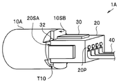
- the imaging device 1 of the present embodiment includes an optical unit 10, an imaging unit 20, a guide unit 30, and a signal cable 40.
- the tip of the imaging unit 20, the guide unit 30, and the signal cable 40 is disposed in a space S ⁇ b> 10 in which the optical unit 10 is extended in the direction of the optical axis (O).
- the imaging device 1 specially designed for endoscopes has a small outside diameter, for example 5 mm or less, which is the same as the outside diameter of the optical unit 10.
- the imaging device 1 is also ultra-small, for example, 10 mm or less in length in the optical axis direction.
- An optical unit 10 having an entrance surface 10SA and an exit surface 10SB facing the entrance surface 10SA includes a frame member 15 and an optical member 11.
- a plurality of optical members 11A to 11D are disposed on the lens frame with the optical axis O at the center.
- the optical members 11A, 11B, and 11D are lenses, and the optical member 11C is a parallel flat filter made of an infrared cut material that removes infrared light.
- the optical member 11 is inserted into the through hole H15 of the frame member (optical holder) 15.
- the frame member 15 and the lens frame of the optical member 11 may be an integral member.
- the imaging unit 20 has a light receiving surface 20SA and a rear surface 20SB facing the light receiving surface 20SA and four side surfaces 20SS.
- a plurality of semiconductor elements 22 to 27 including an imaging element 22 to which a cover glass 21 is adhered are stacked.
- the imaging element 22 photoelectrically converts incident light from the optical unit 10 and outputs an imaging signal.
- optical members such as a plurality of lenses may be disposed on the front surface of the imaging device 22 of the imaging unit 20.
- an optical member 21A such as a convex lens may be disposed on the front surface of the cover glass 21.
- the optical unit 10 may be an extended lens unit of the imaging unit 20 in which optical members such as a plurality of lenses are disposed.
- the imaging device 22 has a light receiving unit 22A formed of a CCD or a CMOS imaging unit.
- the imaging device 22 may be either a front side illumination (FSI) type image sensor or a back side illumination (BSI) type image sensor.
- FSI front side illumination
- BSI back side illumination
- the semiconductor elements 23 to 27 perform primary processing of an imaging signal output from the imaging element 22 and process a control signal for controlling the imaging element 22.
- the semiconductor elements 23 to 27 include an AD conversion circuit, a memory, a transmission output circuit, a filter circuit, a thin film capacitor, a thin film inductor, and the like.
- the number of semiconductor elements 23 to 27 included in the imaging unit 20 is, for example, three or more and ten or less.
- the plurality of semiconductor elements 22 to 27 are electrically connected to each other through the through wiring (not shown), and are disposed on the rear surface of the semiconductor element 27 disposed at the rearmost side, that is, on the rear surface 20SB of the imaging unit 20.
- a plurality of connection electrodes 20P are disposed.
- the imaging unit 20 is manufactured by a cutting process of a laminated wafer in which a cover glass wafer, an imaging wafer including a plurality of imaging elements 22, and a plurality of element wafers each including a plurality of semiconductor elements 23 to 27 are laminated. Ru. For this reason, the imaging unit 20 is a rectangular solid of which the four side surfaces 20SS have a relatively large area. The side surface 20SS may be coated with a light shielding resin.
- a plurality of signal cables 40 for supplying power to the imaging unit 20 and transmitting an imaging signal are joined to the respective connection electrodes 20P.
- imaging is performed via a relay member such as a MID three-dimensional wiring board in which the signal cable 40 is joined to the connection electrode 20P of the imaging unit 20, a Si interposer, a TAB tape with flying leads, a ceramic wiring board, or a glass wiring board. It may be connected to the unit 20.
- the relay member is also designed to be accommodated in the space S10.
- the front portion of the guide portion 30 is fixed to the outer peripheral portion of the light emission surface 10 ⁇ / b> SB of the optical unit 10.
- the guide portion 30 is bonded to the emission surface 10 ⁇ / b> SB via the first adhesive 32.
- the guide part 30 may be inserted in the hole of the radiation
- the guide portion 30 may be integral with the optical unit 10, that is, be part of the optical unit 10.
- the imaging unit 20 is a laminated element in which the cover glass 21 and the plurality of elements 22 to 27 are laminated, the length in the optical axis direction is longer than the imaging element 22 in which the other semiconductor elements 23 to 27 are not laminated. Is long. Since the area of the side surface 20SS of the imaging unit 20 is large, the imaging device 1 can stably fix the contact surface 30SS1 of the guide unit 30.
- the contact surfaces 30SS of the four guide portions 30 are in contact with the four side surfaces 20SS of the rectangular parallelepiped imaging unit 20. For this reason, the relative position between the optical unit 10 and the imaging unit 20 in the optical axis orthogonal direction (in-plane direction) is defined by the guide portion 30. That is, the optical axis of the optical unit 10 and the optical axis of the imaging unit 20 are automatically positioned by the four guide portions 30.
- the imaging device 1 can fix the optical unit 10 and the imaging unit 20 precisely and stably even if it is ultra-compact, productivity is high.
- the contact surfaces 30SS of at least two guide portions 30 which are disposed orthogonal to each other may be in contact with the two side surfaces 20SS of the imaging unit 20. Even if only one guide portion 30 is provided, one of two in-plane directions is defined. Further, the plurality of guide portions 30 need not all have the same shape.
- the imaging device 1 there is a gap (space) having a length G between the emission surface 10 ⁇ / b> SB of the optical unit 10 and the light receiving surface 20 ⁇ / b> SA of the imaging unit 20.
- the distance between the optical unit 10 and the imaging unit 20, that is, the optical path length can be adjusted for each device.
- the emission surface 10SB of the optical unit 10A is bonded to the light receiving surface 20SA of the imaging unit 20 via the first adhesive 32.
- the distance between the optical unit 10 and the imaging unit 20, that is, the optical path length is uniquely defined.
- the light path area of the exit surface 10SB of the optical unit 10A is an aperture.
- the imaging device 1A has stable optical characteristics because there is no possibility that the excess first adhesive 32 intrudes into the opening of the emission surface 10SB.
- the guide portion 30B is a member integral with the optical unit 10B. That is, the optical unit 10B includes four guide portions 30B protruding rearward from the emission surface 10SB.
- the guide portion 30B is a curved surface whose outer surface is continuous with the outer surface of the optical unit 10B.
- the inner surface of the guide portion 30B is a contact surface 30SS in contact with the side surface 20SS of the imaging unit 20B.
- the imaging unit 20B is a hexagonal prism in which the corner in the direction parallel to the optical axis of the rectangular parallelepiped is chamfered.
- Four of the six side surfaces 20SS of the imaging unit 20B are bonded to the contact surfaces of the guide portion 30B.
- the imaging device 1B can achieve high image quality without increasing the outer diameter.
- the imaging unit 20 of the imaging devices 1 and 1A was a rectangular solid (square pole).
- the imaging unit of the present invention may be a hexagonal prism whose corner is chamfered as in the imaging device 1B, or may be a substantially rectangular parallelepiped having a curved surface.
- the optical unit may be a polygonal cylinder or a substantially rectangular parallelepiped having a curved surface.
- a groove (notch) T30 having an opening at the rear end is present on the contact surface 30SS of the guide portion 30C.
- the second adhesive 31 is also disposed in the groove T30.
- the imaging device 1C not only the guide surface 30SS but also the inner surface of the groove T30 is fixed to the side surface 20SS of the imaging unit 20 via the second adhesive 31 in the imaging device 1C. For this reason, the optical unit 10 and the imaging unit 20 are firmly fixed.
- the guide 30 has a hole in place of the groove, or a groove and a hole, the same effect as that of the imaging device 1C is obtained. Further, at least one of the plurality of guide portions 30 may have a groove or the like.
- the side electrode 20SP is disposed on the side surface 20SS.
- the side electrode 20S is, for example, a common ground potential electrode of the plurality of semiconductor elements 22 to 27.
- the guide portion 30D is disposed in the imaging unit 20D such that the side electrode 20SP is disposed at the opening of the groove T30.
- One ground potential cable 40D of the plurality of signal cables 40 is inserted into the groove T30 and joined to the side electrode 20SP.
- the side electrode 20SP may be disposed on at least one side surface 20SS of the plurality of side surfaces 20SS, and the groove T30 may be provided in at least one guide portion 30D of the plurality of guide portions 30.
- the imaging unit 20D can easily position the ground potential cable 40D at the position of the side electrode 20SP of the imaging unit 20D. That is, the width of the groove T30 is set to be substantially the same (strictly, slightly larger) as the outer skin of the ground potential cable 40D.
- the tip of the ground potential cable 40D is also disposed inside the space S10 in which the optical unit 10 is extended in the direction of the optical axis (O).
- the contact surface 30SS of the guide portion 30E has a groove (a notch) T30 whose rear end is an opening.
- the frame member 15 including the guide portion 30E of the optical unit 10E is made of a conductor integral with the lens frame of the optical member 11, for example, stainless steel whose surface is plated with copper.
- the signal cable 40E1 which is a ground potential line inserted in the groove T30, is soldered to the side electrode 20SP and the frame member 15.
- the width of the groove T30 is set to be substantially the same (strictly slightly larger) as the core of the ground potential cable 40D.
- the frame member 15E since the frame member 15E is at the ground potential, there is no possibility of charging to adversely affect the imaging device 22 and the like.
- the outer surface of the frame member 15 may be covered with an insulating resin.
- the guide unit 30E may be soldered without the imaging unit 20 and the second adhesive 31 interposed therebetween.
- the contact surface 30SS of the guide portion 30F has a groove (a notch) T30 whose rear end is an opening.
- the frame member 15 including the guide portion 30F of the optical unit 10E is made of, for example, a MID (Molded Interconnect Device) three-dimensional wiring board having surface wiring.
- the signal cables 40F1 and 40F2 are joined to the wirings made of the conductors of the respective guide portions 30F.
- the signal cable 40F1 which is a ground potential line, is joined to the side electrode (not shown) of the imaging unit 20F via the wiring 10P1 of the guide portion 30F.
- the signal cable 40F2 which is a power line is joined to another side electrode (not shown) of the imaging unit 20F via another wire 10P2 of the guide portion 30F.
- the signal cable 40F2 which is a power line is joined at a distance from the signal cable 40 for transmitting an imaging signal or the like, there is no possibility that the imaging signal or the like is adversely affected by the power signal.
- the tip of the signal cable 40F1 which is the ground potential and the tip of the signal cable 40F2 which is the power line are also disposed inside the space S10 which extends the optical unit 10 in the direction of the optical axis (O).
- an endoscope system 8 including the endoscope 9 of the present embodiment includes an endoscope 9, a processor 80, a light source device 81, and a monitor 82.
- the endoscope 9 has an insertion portion 90, an operation portion 91, and a universal cord 92.
- the insertion portion 90 is inserted into the body cavity of the subject, and the in-vivo image of the subject is captured to output an image signal.
- the insertion portion 90 has a distal end portion 90A on which the imaging devices 1, 1A to 1F (hereinafter referred to as the imaging device 1 etc.) are disposed, and a bendable bending portion 90B connected to the proximal end side of the distal end portion 90A. And a flexible portion 90C provided on the base end side of the curved portion 90B. The bending portion 90B bends by the operation of the operation portion 91.
- the endoscope 9 may be a rigid endoscope or a capsule endoscope.
- an operation portion 91 provided with various buttons for operating the endoscope 9 is disposed.
- the light source device 81 has, for example, a white LED.
- the illumination light emitted from the light source device 81 is guided to the distal end portion 90A via a universal code 92 and a light guide (not shown) which inserts the insertion portion 90, and illuminates the subject.
- the endoscope 9 has an insertion portion 90, an operation portion 91, and a universal cord 92, and passes through the insertion portion 90 an imaging signal output from the imaging device 1 or the like disposed at the distal end portion 90A of the insertion portion 90.
- Signal cable 40 is transmitted.
- the endoscope 9 Since the imaging device 1 is ultra-compact and high in productivity, the endoscope 9 is minimally invasive and has high productivity because the diameter of the distal end portion 90A of the insertion portion 90 is small. In addition, the endoscope having the imaging devices 1A to 1F has the effects of the respective imaging devices.
Abstract
Un dispositif d'imagerie 1 comprend : une unité optique 10 dans laquelle chacun d'une pluralité d'éléments optiques 11A à 11D est disposé autour d'un axe optique O, ladite unité optique ayant une surface d'incidence 10SA et une surface d'émission 10SB; une unité d'imagerie 20 dans laquelle une pluralité d'éléments 22-27 comprenant un élément d'imagerie 22 sont disposés en couches, ladite unité d'imagerie ayant une surface de réception de lumière 20SA, une surface arrière 20SB, et quatre surfaces latérales 20SS; des parties de guidage 30 dans lesquelles une partie avant est fixée à la surface d'émission 10SB de l'unité optique 10, lesdites parties de guidage ayant, dans une partie arrière de celle-ci, des surfaces de contact 30SS qui entrent en contact avec les surfaces latérales 10SS de l'unité d'imagerie 20 et sont fixées à celles-ci; et un câble de signal 40 qui est électriquement connecté à l'unité d'imagerie 20.
Priority Applications (2)
| Application Number | Priority Date | Filing Date | Title |
|---|---|---|---|
| PCT/JP2017/018648 WO2018211652A1 (fr) | 2017-05-18 | 2017-05-18 | Dispositif d'imagerie et endoscope |
| US16/676,642 US11179025B2 (en) | 2017-05-18 | 2019-11-07 | Image pickup apparatus and endoscope |
Applications Claiming Priority (1)
| Application Number | Priority Date | Filing Date | Title |
|---|---|---|---|
| PCT/JP2017/018648 WO2018211652A1 (fr) | 2017-05-18 | 2017-05-18 | Dispositif d'imagerie et endoscope |
Related Child Applications (1)
| Application Number | Title | Priority Date | Filing Date |
|---|---|---|---|
| US16/676,642 Continuation US11179025B2 (en) | 2017-05-18 | 2019-11-07 | Image pickup apparatus and endoscope |
Publications (1)
| Publication Number | Publication Date |
|---|---|
| WO2018211652A1 true WO2018211652A1 (fr) | 2018-11-22 |
Family
ID=64273588
Family Applications (1)
| Application Number | Title | Priority Date | Filing Date |
|---|---|---|---|
| PCT/JP2017/018648 WO2018211652A1 (fr) | 2017-05-18 | 2017-05-18 | Dispositif d'imagerie et endoscope |
Country Status (2)
| Country | Link |
|---|---|
| US (1) | US11179025B2 (fr) |
| WO (1) | WO2018211652A1 (fr) |
Cited By (1)
| Publication number | Priority date | Publication date | Assignee | Title |
|---|---|---|---|---|
| WO2021176551A1 (fr) * | 2020-03-03 | 2021-09-10 | オリンパス株式会社 | Endoscope et module d'imagerie |
Families Citing this family (1)
| Publication number | Priority date | Publication date | Assignee | Title |
|---|---|---|---|---|
| US11963667B2 (en) * | 2021-11-26 | 2024-04-23 | Altek Biotechnology Corporation | Endoscopic image capturing assembly and endoscopic device therewith |
Citations (4)
| Publication number | Priority date | Publication date | Assignee | Title |
|---|---|---|---|---|
| JPS63118120A (ja) * | 1987-10-08 | 1988-05-23 | Olympus Optical Co Ltd | 撮像装置 |
| JPH01201229A (ja) * | 1988-02-04 | 1989-08-14 | Olympus Optical Co Ltd | 電子内視鏡システム |
| JPH0258404U (fr) * | 1988-10-25 | 1990-04-26 | ||
| WO2017073440A1 (fr) * | 2015-10-27 | 2017-05-04 | オリンパス株式会社 | Endoscope |
Family Cites Families (6)
| Publication number | Priority date | Publication date | Assignee | Title |
|---|---|---|---|---|
| CN102711583B (zh) * | 2010-02-01 | 2014-10-01 | 奥林巴斯医疗株式会社 | 内窥镜用摄像单元 |
| JP2011237525A (ja) * | 2010-05-07 | 2011-11-24 | Olympus Corp | 撮像モジュール |
| EP3061384B8 (fr) | 2014-05-21 | 2018-08-08 | Olympus Corporation | Unité de capture d'image et endoscope |
| JP5866565B1 (ja) * | 2014-12-22 | 2016-02-17 | パナソニックIpマネジメント株式会社 | 内視鏡 |
| US9838576B2 (en) * | 2015-08-31 | 2017-12-05 | Panasonic Corporation | Endoscope |
| WO2018079070A1 (fr) * | 2016-10-25 | 2018-05-03 | 富士フイルム株式会社 | Endoscope |
-
2017
- 2017-05-18 WO PCT/JP2017/018648 patent/WO2018211652A1/fr active Application Filing
-
2019
- 2019-11-07 US US16/676,642 patent/US11179025B2/en active Active
Patent Citations (4)
| Publication number | Priority date | Publication date | Assignee | Title |
|---|---|---|---|---|
| JPS63118120A (ja) * | 1987-10-08 | 1988-05-23 | Olympus Optical Co Ltd | 撮像装置 |
| JPH01201229A (ja) * | 1988-02-04 | 1989-08-14 | Olympus Optical Co Ltd | 電子内視鏡システム |
| JPH0258404U (fr) * | 1988-10-25 | 1990-04-26 | ||
| WO2017073440A1 (fr) * | 2015-10-27 | 2017-05-04 | オリンパス株式会社 | Endoscope |
Cited By (1)
| Publication number | Priority date | Publication date | Assignee | Title |
|---|---|---|---|---|
| WO2021176551A1 (fr) * | 2020-03-03 | 2021-09-10 | オリンパス株式会社 | Endoscope et module d'imagerie |
Also Published As
| Publication number | Publication date |
|---|---|
| US11179025B2 (en) | 2021-11-23 |
| US20200069151A1 (en) | 2020-03-05 |
Similar Documents
| Publication | Publication Date | Title |
|---|---|---|
| JP6617054B2 (ja) | 内視鏡 | |
| US11172812B2 (en) | Endoscope | |
| US9462933B2 (en) | Image pickup unit for endoscope | |
| WO2012120734A1 (fr) | Unité d'imagerie et endoscope | |
| US10281710B2 (en) | Imaging module and endoscope apparatus each having a flexible substrate divided into different regions where a chip having a transmission buffer and a drive signal cable are connected to the different regions | |
| JP6539548B2 (ja) | 内視鏡用撮像装置及び内視鏡 | |
| US11435570B2 (en) | Image pickup apparatus for endoscope, endoscope, and manufacturing method of image pickup apparatus for endoscope | |
| WO2014171482A1 (fr) | Dispositif d'imagerie, et endoscope électronique | |
| US10617285B2 (en) | Imaging module with multi-layer substrate and endoscope apparatus | |
| US10972707B2 (en) | Endoscope and method of manufacturing endoscope | |
| US20180325364A1 (en) | Image pickup apparatus and endoscope | |
| WO2018211652A1 (fr) | Dispositif d'imagerie et endoscope | |
| WO2016092991A1 (fr) | Endoscope | |
| US9629524B2 (en) | Image pickup unit for endoscope having first and second leads with differing distances to image pickup device | |
| WO2019176601A1 (fr) | Unité d'imagerie et endoscope oblique | |
| JP2020028628A (ja) | 内視鏡および内視鏡の製造方法 | |
| US11278192B2 (en) | Endoscope | |
| US11445897B2 (en) | Endoscope with holding member having multiple independent wall parts | |
| US11876107B2 (en) | Image pickup apparatus for endoscope and endoscope | |
| JP7029296B2 (ja) | 内視鏡の基板ユニット | |
| JP2014210041A (ja) | 撮像装置および電子内視鏡 | |
| WO2023233524A1 (fr) | Unité d'imagerie et endoscope | |
| JPS6066222A (ja) | 内視鏡 | |
| WO2020179067A1 (fr) | Transducteur optique endoscopique, dispositif d'imagerie endoscopique et endoscope | |
| JP2022179301A (ja) | 内視鏡撮像装置及び内視鏡 |
Legal Events
| Date | Code | Title | Description |
|---|---|---|---|
| 121 | Ep: the epo has been informed by wipo that ep was designated in this application |
Ref document number: 17910188 Country of ref document: EP Kind code of ref document: A1 |
|
| NENP | Non-entry into the national phase |
Ref country code: DE |
|
| 122 | Ep: pct application non-entry in european phase |
Ref document number: 17910188 Country of ref document: EP Kind code of ref document: A1 |
|
| NENP | Non-entry into the national phase |
Ref country code: JP |