WO2018211652A1 - Imaging device and endoscope - Google Patents
Imaging device and endoscope Download PDFInfo
- Publication number
- WO2018211652A1 WO2018211652A1 PCT/JP2017/018648 JP2017018648W WO2018211652A1 WO 2018211652 A1 WO2018211652 A1 WO 2018211652A1 JP 2017018648 W JP2017018648 W JP 2017018648W WO 2018211652 A1 WO2018211652 A1 WO 2018211652A1
- Authority
- WO
- WIPO (PCT)
- Prior art keywords
- imaging
- unit
- optical
- imaging device
- imaging unit
- Prior art date
Links
Images


Classifications
-
- A—HUMAN NECESSITIES
- A61—MEDICAL OR VETERINARY SCIENCE; HYGIENE
- A61B—DIAGNOSIS; SURGERY; IDENTIFICATION
- A61B1/00—Instruments for performing medical examinations of the interior of cavities or tubes of the body by visual or photographical inspection, e.g. endoscopes; Illuminating arrangements therefor
- A61B1/04—Instruments for performing medical examinations of the interior of cavities or tubes of the body by visual or photographical inspection, e.g. endoscopes; Illuminating arrangements therefor combined with photographic or television appliances
- A61B1/05—Instruments for performing medical examinations of the interior of cavities or tubes of the body by visual or photographical inspection, e.g. endoscopes; Illuminating arrangements therefor combined with photographic or television appliances characterised by the image sensor, e.g. camera, being in the distal end portion
- A61B1/051—Details of CCD assembly
-
- A—HUMAN NECESSITIES
- A61—MEDICAL OR VETERINARY SCIENCE; HYGIENE
- A61B—DIAGNOSIS; SURGERY; IDENTIFICATION
- A61B1/00—Instruments for performing medical examinations of the interior of cavities or tubes of the body by visual or photographical inspection, e.g. endoscopes; Illuminating arrangements therefor
- A61B1/00002—Operational features of endoscopes
- A61B1/00043—Operational features of endoscopes provided with output arrangements
- A61B1/00045—Display arrangement
-
- A—HUMAN NECESSITIES
- A61—MEDICAL OR VETERINARY SCIENCE; HYGIENE
- A61B—DIAGNOSIS; SURGERY; IDENTIFICATION
- A61B1/00—Instruments for performing medical examinations of the interior of cavities or tubes of the body by visual or photographical inspection, e.g. endoscopes; Illuminating arrangements therefor
- A61B1/00064—Constructional details of the endoscope body
- A61B1/00071—Insertion part of the endoscope body
- A61B1/0008—Insertion part of the endoscope body characterised by distal tip features
- A61B1/00096—Optical elements
-
- A—HUMAN NECESSITIES
- A61—MEDICAL OR VETERINARY SCIENCE; HYGIENE
- A61B—DIAGNOSIS; SURGERY; IDENTIFICATION
- A61B1/00—Instruments for performing medical examinations of the interior of cavities or tubes of the body by visual or photographical inspection, e.g. endoscopes; Illuminating arrangements therefor
- A61B1/06—Instruments for performing medical examinations of the interior of cavities or tubes of the body by visual or photographical inspection, e.g. endoscopes; Illuminating arrangements therefor with illuminating arrangements
- A61B1/0661—Endoscope light sources
- A61B1/0676—Endoscope light sources at distal tip of an endoscope
-
- G—PHYSICS
- G02—OPTICS
- G02B—OPTICAL ELEMENTS, SYSTEMS OR APPARATUS
- G02B23/00—Telescopes, e.g. binoculars; Periscopes; Instruments for viewing the inside of hollow bodies; Viewfinders; Optical aiming or sighting devices
- G02B23/24—Instruments or systems for viewing the inside of hollow bodies, e.g. fibrescopes
- G02B23/2407—Optical details
- G02B23/2423—Optical details of the distal end
- G02B23/243—Objectives for endoscopes
Definitions
- the present invention relates to an imaging device including an optical unit and an imaging unit, and an endoscope including an imaging device including an optical unit and an imaging unit.
- an ultra-compact imaging unit that processes and outputs an imaging signal output from an imaging device, in which a plurality of semiconductor devices including the imaging device are stacked.
- Japanese Patent No. 589 7235 discloses an imaging device in which an optical unit is adhered to an imaging element to which a cover glass is adhered.
- An embodiment of the present invention aims to provide an endoscope having a highly productive imaging device and a highly productive imaging device.
- An imaging apparatus includes an optical unit having a light entrance surface and an exit surface facing the light entrance surface, wherein a plurality of optical members are disposed about an optical axis, a light receiving surface, and a back surface facing the light receiving surface.
- a guide portion fixed at the rear and having a contact surface in contact with and fixed to the side surface of the imaging unit, and a signal cable electrically connected to the imaging unit are provided.
- An endoscope includes an imaging device, and the imaging device has an incident surface and an exit surface opposite to the incident surface, and a plurality of optical members are disposed around an optical axis to form an optical unit.
- an imaging unit including a plurality of elements including a light receiving surface, a back surface facing the light receiving surface, and a side surface facing the light receiving surface and including an image sensor that photoelectrically converts light incident from the optical unit and outputs an imaging signal.
- a front portion is fixed to the light emitting surface of the optical unit, and a guide portion having a contact surface fixed to the side surface of the imaging unit in contact with the side surface of the imaging unit and electrically connected to the imaging unit And a signal cable.
- an endoscope having a highly productive imaging device and a highly productive imaging device.
- FIG. 5C is a cross-sectional view of the imaging device of Modification Example 2 of the first embodiment, taken along the line VB-VB of FIG. 5A.
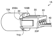
- the imaging device 1 of the present embodiment includes an optical unit 10, an imaging unit 20, a guide unit 30, and a signal cable 40.
- the tip of the imaging unit 20, the guide unit 30, and the signal cable 40 is disposed in a space S ⁇ b> 10 in which the optical unit 10 is extended in the direction of the optical axis (O).
- the imaging device 1 specially designed for endoscopes has a small outside diameter, for example 5 mm or less, which is the same as the outside diameter of the optical unit 10.
- the imaging device 1 is also ultra-small, for example, 10 mm or less in length in the optical axis direction.
- An optical unit 10 having an entrance surface 10SA and an exit surface 10SB facing the entrance surface 10SA includes a frame member 15 and an optical member 11.
- a plurality of optical members 11A to 11D are disposed on the lens frame with the optical axis O at the center.
- the optical members 11A, 11B, and 11D are lenses, and the optical member 11C is a parallel flat filter made of an infrared cut material that removes infrared light.
- the optical member 11 is inserted into the through hole H15 of the frame member (optical holder) 15.
- the frame member 15 and the lens frame of the optical member 11 may be an integral member.
- the imaging unit 20 has a light receiving surface 20SA and a rear surface 20SB facing the light receiving surface 20SA and four side surfaces 20SS.
- a plurality of semiconductor elements 22 to 27 including an imaging element 22 to which a cover glass 21 is adhered are stacked.
- the imaging element 22 photoelectrically converts incident light from the optical unit 10 and outputs an imaging signal.
- optical members such as a plurality of lenses may be disposed on the front surface of the imaging device 22 of the imaging unit 20.
- an optical member 21A such as a convex lens may be disposed on the front surface of the cover glass 21.
- the optical unit 10 may be an extended lens unit of the imaging unit 20 in which optical members such as a plurality of lenses are disposed.
- the imaging device 22 has a light receiving unit 22A formed of a CCD or a CMOS imaging unit.
- the imaging device 22 may be either a front side illumination (FSI) type image sensor or a back side illumination (BSI) type image sensor.
- FSI front side illumination
- BSI back side illumination
- the semiconductor elements 23 to 27 perform primary processing of an imaging signal output from the imaging element 22 and process a control signal for controlling the imaging element 22.
- the semiconductor elements 23 to 27 include an AD conversion circuit, a memory, a transmission output circuit, a filter circuit, a thin film capacitor, a thin film inductor, and the like.
- the number of semiconductor elements 23 to 27 included in the imaging unit 20 is, for example, three or more and ten or less.
- the plurality of semiconductor elements 22 to 27 are electrically connected to each other through the through wiring (not shown), and are disposed on the rear surface of the semiconductor element 27 disposed at the rearmost side, that is, on the rear surface 20SB of the imaging unit 20.
- a plurality of connection electrodes 20P are disposed.
- the imaging unit 20 is manufactured by a cutting process of a laminated wafer in which a cover glass wafer, an imaging wafer including a plurality of imaging elements 22, and a plurality of element wafers each including a plurality of semiconductor elements 23 to 27 are laminated. Ru. For this reason, the imaging unit 20 is a rectangular solid of which the four side surfaces 20SS have a relatively large area. The side surface 20SS may be coated with a light shielding resin.
- a plurality of signal cables 40 for supplying power to the imaging unit 20 and transmitting an imaging signal are joined to the respective connection electrodes 20P.
- imaging is performed via a relay member such as a MID three-dimensional wiring board in which the signal cable 40 is joined to the connection electrode 20P of the imaging unit 20, a Si interposer, a TAB tape with flying leads, a ceramic wiring board, or a glass wiring board. It may be connected to the unit 20.
- the relay member is also designed to be accommodated in the space S10.
- the front portion of the guide portion 30 is fixed to the outer peripheral portion of the light emission surface 10 ⁇ / b> SB of the optical unit 10.
- the guide portion 30 is bonded to the emission surface 10 ⁇ / b> SB via the first adhesive 32.
- the guide part 30 may be inserted in the hole of the radiation
- the guide portion 30 may be integral with the optical unit 10, that is, be part of the optical unit 10.
- the imaging unit 20 is a laminated element in which the cover glass 21 and the plurality of elements 22 to 27 are laminated, the length in the optical axis direction is longer than the imaging element 22 in which the other semiconductor elements 23 to 27 are not laminated. Is long. Since the area of the side surface 20SS of the imaging unit 20 is large, the imaging device 1 can stably fix the contact surface 30SS1 of the guide unit 30.
- the contact surfaces 30SS of the four guide portions 30 are in contact with the four side surfaces 20SS of the rectangular parallelepiped imaging unit 20. For this reason, the relative position between the optical unit 10 and the imaging unit 20 in the optical axis orthogonal direction (in-plane direction) is defined by the guide portion 30. That is, the optical axis of the optical unit 10 and the optical axis of the imaging unit 20 are automatically positioned by the four guide portions 30.
- the imaging device 1 can fix the optical unit 10 and the imaging unit 20 precisely and stably even if it is ultra-compact, productivity is high.
- the contact surfaces 30SS of at least two guide portions 30 which are disposed orthogonal to each other may be in contact with the two side surfaces 20SS of the imaging unit 20. Even if only one guide portion 30 is provided, one of two in-plane directions is defined. Further, the plurality of guide portions 30 need not all have the same shape.
- the imaging device 1 there is a gap (space) having a length G between the emission surface 10 ⁇ / b> SB of the optical unit 10 and the light receiving surface 20 ⁇ / b> SA of the imaging unit 20.
- the distance between the optical unit 10 and the imaging unit 20, that is, the optical path length can be adjusted for each device.
- the emission surface 10SB of the optical unit 10A is bonded to the light receiving surface 20SA of the imaging unit 20 via the first adhesive 32.
- the distance between the optical unit 10 and the imaging unit 20, that is, the optical path length is uniquely defined.
- the light path area of the exit surface 10SB of the optical unit 10A is an aperture.
- the imaging device 1A has stable optical characteristics because there is no possibility that the excess first adhesive 32 intrudes into the opening of the emission surface 10SB.
- the guide portion 30B is a member integral with the optical unit 10B. That is, the optical unit 10B includes four guide portions 30B protruding rearward from the emission surface 10SB.
- the guide portion 30B is a curved surface whose outer surface is continuous with the outer surface of the optical unit 10B.
- the inner surface of the guide portion 30B is a contact surface 30SS in contact with the side surface 20SS of the imaging unit 20B.
- the imaging unit 20B is a hexagonal prism in which the corner in the direction parallel to the optical axis of the rectangular parallelepiped is chamfered.
- Four of the six side surfaces 20SS of the imaging unit 20B are bonded to the contact surfaces of the guide portion 30B.
- the imaging device 1B can achieve high image quality without increasing the outer diameter.
- the imaging unit 20 of the imaging devices 1 and 1A was a rectangular solid (square pole).
- the imaging unit of the present invention may be a hexagonal prism whose corner is chamfered as in the imaging device 1B, or may be a substantially rectangular parallelepiped having a curved surface.
- the optical unit may be a polygonal cylinder or a substantially rectangular parallelepiped having a curved surface.
- a groove (notch) T30 having an opening at the rear end is present on the contact surface 30SS of the guide portion 30C.
- the second adhesive 31 is also disposed in the groove T30.
- the imaging device 1C not only the guide surface 30SS but also the inner surface of the groove T30 is fixed to the side surface 20SS of the imaging unit 20 via the second adhesive 31 in the imaging device 1C. For this reason, the optical unit 10 and the imaging unit 20 are firmly fixed.
- the guide 30 has a hole in place of the groove, or a groove and a hole, the same effect as that of the imaging device 1C is obtained. Further, at least one of the plurality of guide portions 30 may have a groove or the like.
- the side electrode 20SP is disposed on the side surface 20SS.
- the side electrode 20S is, for example, a common ground potential electrode of the plurality of semiconductor elements 22 to 27.
- the guide portion 30D is disposed in the imaging unit 20D such that the side electrode 20SP is disposed at the opening of the groove T30.
- One ground potential cable 40D of the plurality of signal cables 40 is inserted into the groove T30 and joined to the side electrode 20SP.
- the side electrode 20SP may be disposed on at least one side surface 20SS of the plurality of side surfaces 20SS, and the groove T30 may be provided in at least one guide portion 30D of the plurality of guide portions 30.
- the imaging unit 20D can easily position the ground potential cable 40D at the position of the side electrode 20SP of the imaging unit 20D. That is, the width of the groove T30 is set to be substantially the same (strictly, slightly larger) as the outer skin of the ground potential cable 40D.
- the tip of the ground potential cable 40D is also disposed inside the space S10 in which the optical unit 10 is extended in the direction of the optical axis (O).
- the contact surface 30SS of the guide portion 30E has a groove (a notch) T30 whose rear end is an opening.
- the frame member 15 including the guide portion 30E of the optical unit 10E is made of a conductor integral with the lens frame of the optical member 11, for example, stainless steel whose surface is plated with copper.
- the signal cable 40E1 which is a ground potential line inserted in the groove T30, is soldered to the side electrode 20SP and the frame member 15.
- the width of the groove T30 is set to be substantially the same (strictly slightly larger) as the core of the ground potential cable 40D.
- the frame member 15E since the frame member 15E is at the ground potential, there is no possibility of charging to adversely affect the imaging device 22 and the like.
- the outer surface of the frame member 15 may be covered with an insulating resin.
- the guide unit 30E may be soldered without the imaging unit 20 and the second adhesive 31 interposed therebetween.
- the contact surface 30SS of the guide portion 30F has a groove (a notch) T30 whose rear end is an opening.
- the frame member 15 including the guide portion 30F of the optical unit 10E is made of, for example, a MID (Molded Interconnect Device) three-dimensional wiring board having surface wiring.
- the signal cables 40F1 and 40F2 are joined to the wirings made of the conductors of the respective guide portions 30F.
- the signal cable 40F1 which is a ground potential line, is joined to the side electrode (not shown) of the imaging unit 20F via the wiring 10P1 of the guide portion 30F.
- the signal cable 40F2 which is a power line is joined to another side electrode (not shown) of the imaging unit 20F via another wire 10P2 of the guide portion 30F.
- the signal cable 40F2 which is a power line is joined at a distance from the signal cable 40 for transmitting an imaging signal or the like, there is no possibility that the imaging signal or the like is adversely affected by the power signal.
- the tip of the signal cable 40F1 which is the ground potential and the tip of the signal cable 40F2 which is the power line are also disposed inside the space S10 which extends the optical unit 10 in the direction of the optical axis (O).
- an endoscope system 8 including the endoscope 9 of the present embodiment includes an endoscope 9, a processor 80, a light source device 81, and a monitor 82.
- the endoscope 9 has an insertion portion 90, an operation portion 91, and a universal cord 92.
- the insertion portion 90 is inserted into the body cavity of the subject, and the in-vivo image of the subject is captured to output an image signal.
- the insertion portion 90 has a distal end portion 90A on which the imaging devices 1, 1A to 1F (hereinafter referred to as the imaging device 1 etc.) are disposed, and a bendable bending portion 90B connected to the proximal end side of the distal end portion 90A. And a flexible portion 90C provided on the base end side of the curved portion 90B. The bending portion 90B bends by the operation of the operation portion 91.
- the endoscope 9 may be a rigid endoscope or a capsule endoscope.
- an operation portion 91 provided with various buttons for operating the endoscope 9 is disposed.
- the light source device 81 has, for example, a white LED.
- the illumination light emitted from the light source device 81 is guided to the distal end portion 90A via a universal code 92 and a light guide (not shown) which inserts the insertion portion 90, and illuminates the subject.
- the endoscope 9 has an insertion portion 90, an operation portion 91, and a universal cord 92, and passes through the insertion portion 90 an imaging signal output from the imaging device 1 or the like disposed at the distal end portion 90A of the insertion portion 90.
- Signal cable 40 is transmitted.
- the endoscope 9 Since the imaging device 1 is ultra-compact and high in productivity, the endoscope 9 is minimally invasive and has high productivity because the diameter of the distal end portion 90A of the insertion portion 90 is small. In addition, the endoscope having the imaging devices 1A to 1F has the effects of the respective imaging devices.
Landscapes
- Health & Medical Sciences (AREA)
- Life Sciences & Earth Sciences (AREA)
- Surgery (AREA)
- Physics & Mathematics (AREA)
- Optics & Photonics (AREA)
- Engineering & Computer Science (AREA)
- Biomedical Technology (AREA)
- Nuclear Medicine, Radiotherapy & Molecular Imaging (AREA)
- Pathology (AREA)
- Radiology & Medical Imaging (AREA)
- Veterinary Medicine (AREA)
- Public Health (AREA)
- Biophysics (AREA)
- Heart & Thoracic Surgery (AREA)
- Medical Informatics (AREA)
- Molecular Biology (AREA)
- Animal Behavior & Ethology (AREA)
- General Health & Medical Sciences (AREA)
- General Physics & Mathematics (AREA)
- Astronomy & Astrophysics (AREA)
- Endoscopes (AREA)
Abstract
An imaging device 1 comprises: an optical unit 10 in which each of a plurality of optical members 11A to 11D is disposed around an optical axis O, said optical unit having an incidence surface 10SA and an emission surface 10SB; an imaging unit 20 in which a plurality of elements 22-27 including an imaging element 22 are layered, said imaging unit having a light reception surface 20SA, a rear surface 20SB, and four side surfaces 20SS; guiding parts 30 in which a front part is secured to the emission surface 10SB of the optical unit 10, said guiding parts having, in a rear part thereof, contact surfaces 30SS that make contact with and are secured to the side surfaces 10SS of the imaging unit 20; and a signal cable 40 that is electrically connected to the imaging unit 20.
Description
本発明は、光学ユニットと撮像ユニットとを具備する撮像装置、および、光学ユニットと撮像ユニットとを具備する撮像装置を有する内視鏡に関する。
The present invention relates to an imaging device including an optical unit and an imaging unit, and an endoscope including an imaging device including an optical unit and an imaging unit.
近年、撮像素子を含む複数の半導体素子が積層された、撮像素子が出力した撮像信号を処理して出力する超小型の撮像ユニットが開発されている。内視鏡に上記撮像ユニットを用いることで先端部の細径化および高機能化を図ることができる。
In recent years, an ultra-compact imaging unit has been developed that processes and outputs an imaging signal output from an imaging device, in which a plurality of semiconductor devices including the imaging device are stacked. By using the above-described imaging unit for an endoscope, it is possible to reduce the diameter of the tip end and to enhance the function.
少量多品種である複数種類の内視鏡を製造するため、標準仕様の撮像ユニットに、内視鏡の仕様に応じた光学ユニットを取り付けることが検討されている。
In order to manufacture a plurality of types of endoscopes of a small amount and a wide variety, it has been considered to attach an optical unit according to the specifications of the endoscope to an imaging unit of a standard specification.
なお、日本国特許第5897235号公報には、光学ユニットをカバーガラスが接着された撮像素子に接着した撮像装置が開示されている。
Japanese Patent No. 589 7235 discloses an imaging device in which an optical unit is adhered to an imaging element to which a cover glass is adhered.
しかし、超小型の撮像ユニットに、超小型の光学ユニットを精度良く取り付けることは容易ではない。
However, it is not easy to precisely attach the ultra-compact optical unit to the ultra-compact imaging unit.
本発明の実施形態は、生産性の高い撮像装置、および生産性の高い撮像装置を有する内視鏡を提供することを目的とする。
An embodiment of the present invention aims to provide an endoscope having a highly productive imaging device and a highly productive imaging device.
実施形態の撮像装置は、入射面と前記入射面と対向する出射面とを有する、複数の光学部材が光軸を中心に配置されている光学ユニットと、受光面と前記受光面と対向する後面と側面とを有する、前記光学ユニットから入射する光を光電変換して撮像信号を出力する撮像素子を含む複数の素子が積層されている撮像ユニットと、前部が前記光学ユニットの前記出射面に固定されており、後部に前記撮像ユニットの前記側面と当接し固定されている当接面のあるガイド部と、前記撮像ユニットと電気的に接続されている信号ケーブルと、を具備する。
An imaging apparatus according to an embodiment includes an optical unit having a light entrance surface and an exit surface facing the light entrance surface, wherein a plurality of optical members are disposed about an optical axis, a light receiving surface, and a back surface facing the light receiving surface. An imaging unit in which a plurality of elements including an imaging element that photoelectrically converts light incident from the optical unit and outputs an imaging signal, and an imaging unit having a front portion on the exit surface of the optical unit A guide portion fixed at the rear and having a contact surface in contact with and fixed to the side surface of the imaging unit, and a signal cable electrically connected to the imaging unit are provided.
別の実施形態の内視鏡は撮像装置を具備し、前記撮像装置は、入射面と前記入射面と対向する出射面とを有する、複数の光学部材が光軸を中心に配置されて光学ユニットと、受光面と前記受光面と対向する後面と側面とを有する、前記光学ユニットから入射する光を光電変換して撮像信号を出力する撮像素子を含む複数の素子が積層されている撮像ユニットと、前部が前記光学ユニットの前記出射面に固定されており、後部に前記撮像ユニットの前記側面と当接し固定されている当接面のあるガイド部と、前記撮像ユニットと電気的に接続されている信号ケーブルと、を具備する。
An endoscope according to another embodiment includes an imaging device, and the imaging device has an incident surface and an exit surface opposite to the incident surface, and a plurality of optical members are disposed around an optical axis to form an optical unit. And an imaging unit including a plurality of elements including a light receiving surface, a back surface facing the light receiving surface, and a side surface facing the light receiving surface and including an image sensor that photoelectrically converts light incident from the optical unit and outputs an imaging signal. A front portion is fixed to the light emitting surface of the optical unit, and a guide portion having a contact surface fixed to the side surface of the imaging unit in contact with the side surface of the imaging unit and electrically connected to the imaging unit And a signal cable.
本発明の実施形態によれば、生産性の高い撮像装置、および生産性の高い撮像装置を有する内視鏡を提供できる。
According to the embodiment of the present invention, it is possible to provide an endoscope having a highly productive imaging device and a highly productive imaging device.
<第1実施形態>
図1~図3に示すように、本実施形態の撮像装置1は、光学ユニット10と撮像ユニット20とガイド部30と信号ケーブル40とを具備する。 First Embodiment
As shown in FIGS. 1 to 3, theimaging device 1 of the present embodiment includes an optical unit 10, an imaging unit 20, a guide unit 30, and a signal cable 40.
図1~図3に示すように、本実施形態の撮像装置1は、光学ユニット10と撮像ユニット20とガイド部30と信号ケーブル40とを具備する。 First Embodiment
As shown in FIGS. 1 to 3, the
なお、以下の説明において、各実施の形態に基づく図面は、模式的なものであり、各部分の厚みと幅との関係、夫々の部分の厚みの比率および相対角度などは現実のものとは異なることに留意すべきであり、図面の相互間においても互いの寸法の関係や比率が異なる部分が含まれている場合がある。また、一部の構成要素の図示を省略することがある。
In the following description, the drawings based on each embodiment are schematic, and the relationship between the thickness and width of each part, the ratio of the thickness of each part, the relative angle, etc. It should be noted that they may be different, and there may be parts where the dimensional relationships and proportions are different among the drawings. Moreover, illustration of some components may be omitted.
撮像装置1は、光学ユニット10を光軸(O)の方向に延長した空間S10の内部に撮像ユニット20とガイド部30と信号ケーブル40の先端部が配設されている。内視鏡用に特化して設計されている撮像装置1は、外径が光学ユニット10の外径と同じ、例えば5mm以下と細径である。なお、撮像装置1は光軸方向の長さも例えば、10mm以下と超小型である。
In the imaging device 1, the tip of the imaging unit 20, the guide unit 30, and the signal cable 40 is disposed in a space S <b> 10 in which the optical unit 10 is extended in the direction of the optical axis (O). The imaging device 1 specially designed for endoscopes has a small outside diameter, for example 5 mm or less, which is the same as the outside diameter of the optical unit 10. The imaging device 1 is also ultra-small, for example, 10 mm or less in length in the optical axis direction.
入射面10SAと入射面10SAと対向する出射面10SBとを有する光学ユニット10は、枠部材15と光学部材11とを含む。光学部材11は複数の光学部材11A~11Dが光軸Oを中心にレンズ枠に配置されている。光学部材11A、11B、11Dはレンズであり、光学部材11Cは赤外線を除去する赤外線カット材料からなる平行平板のフィルタである。光学部材11は、枠部材(光学ホルダ)15の貫通孔H15に挿入されている。後述するように、光学ユニット10は枠部材15と光学部材11のレンズ枠とが一体の部材でもよい。
An optical unit 10 having an entrance surface 10SA and an exit surface 10SB facing the entrance surface 10SA includes a frame member 15 and an optical member 11. In the optical member 11, a plurality of optical members 11A to 11D are disposed on the lens frame with the optical axis O at the center. The optical members 11A, 11B, and 11D are lenses, and the optical member 11C is a parallel flat filter made of an infrared cut material that removes infrared light. The optical member 11 is inserted into the through hole H15 of the frame member (optical holder) 15. As described later, in the optical unit 10, the frame member 15 and the lens frame of the optical member 11 may be an integral member.
撮像ユニット20は、受光面20SAと受光面20SAと対向する後面20SBと4側面20SSとを有する。撮像ユニット20は、カバーガラス21が接着されている撮像素子22を含む複数の半導体素子22~27が積層されている。撮像素子22は、光学ユニット10からの入射光を光電変換して撮像信号を出力する。
The imaging unit 20 has a light receiving surface 20SA and a rear surface 20SB facing the light receiving surface 20SA and four side surfaces 20SS. In the imaging unit 20, a plurality of semiconductor elements 22 to 27 including an imaging element 22 to which a cover glass 21 is adhered are stacked. The imaging element 22 photoelectrically converts incident light from the optical unit 10 and outputs an imaging signal.
なお、撮像ユニット20の撮像素子22の前面に、カバーガラス21だけでなく、複数のレンズ等の光学部材が配設されていてもよい。例えば、図2Cに示す撮像装置1Xの撮像ユニット20Xのように、カバーガラス21の前面に凸レンズ等の光学部材21Aが配設されていてもよい。すなわち、光学ユニット10は、複数のレンズなどの光学部材が配設された撮像ユニット20の拡張レンズユニットであってもよい。
Not only the cover glass 21 but also optical members such as a plurality of lenses may be disposed on the front surface of the imaging device 22 of the imaging unit 20. For example, as in an imaging unit 20X of the imaging device 1X shown in FIG. 2C, an optical member 21A such as a convex lens may be disposed on the front surface of the cover glass 21. That is, the optical unit 10 may be an extended lens unit of the imaging unit 20 in which optical members such as a plurality of lenses are disposed.
撮像素子22は、CCDまたはCMOS撮像部からなる受光部22Aを有する。撮像素子22は、表面照射(FSI:Front Side Illumination)型イメージセンサまたは後面照射(BSI:Back Side Illumination)型イメージセンサのいずれでもよい。
The imaging device 22 has a light receiving unit 22A formed of a CCD or a CMOS imaging unit. The imaging device 22 may be either a front side illumination (FSI) type image sensor or a back side illumination (BSI) type image sensor.
半導体素子23~27は、撮像素子22が出力する撮像信号を1次処理したり、撮像素子22を制御する制御信号を処理したりする。例えば、半導体素子23~27は、AD変換回路、メモリ、伝送出力回路、フィルタ回路、薄膜コンデンサ、および、薄膜インダクタ等を含んでいる。撮像ユニット20が含む半導体素子23~27の数は例えば、3以上10以下である。複数の半導体素子22~27は、それぞれが貫通配線(不図示)を介して電気的に接続されており、最も後方に配置されている半導体素子27の後面、すなわち、撮像ユニット20の後面20SBには、複数の接続電極20Pが配設されている。
The semiconductor elements 23 to 27 perform primary processing of an imaging signal output from the imaging element 22 and process a control signal for controlling the imaging element 22. For example, the semiconductor elements 23 to 27 include an AD conversion circuit, a memory, a transmission output circuit, a filter circuit, a thin film capacitor, a thin film inductor, and the like. The number of semiconductor elements 23 to 27 included in the imaging unit 20 is, for example, three or more and ten or less. The plurality of semiconductor elements 22 to 27 are electrically connected to each other through the through wiring (not shown), and are disposed on the rear surface of the semiconductor element 27 disposed at the rearmost side, that is, on the rear surface 20SB of the imaging unit 20. A plurality of connection electrodes 20P are disposed.
撮像ユニット20は、カバーガラスウエハと、複数の撮像素子22を含む撮像ウエハと、それぞれが複数の半導体素子23~27を含む複数の素子ウエハと、が積層された積層ウエハの切断処理により作製される。このため、撮像ユニット20は、4側面20SSが比較的面積の広い切断面の直方体である。側面20SSに遮光樹脂がコーティングされていてもよい。
The imaging unit 20 is manufactured by a cutting process of a laminated wafer in which a cover glass wafer, an imaging wafer including a plurality of imaging elements 22, and a plurality of element wafers each including a plurality of semiconductor elements 23 to 27 are laminated. Ru. For this reason, the imaging unit 20 is a rectangular solid of which the four side surfaces 20SS have a relatively large area. The side surface 20SS may be coated with a light shielding resin.
撮像ユニット20に電力を供給したり、撮像信号を伝送したりする複数の信号ケーブル40は、それぞれの接続電極20Pと接合されている。なお、信号ケーブル40が、撮像ユニット20の接続電極20Pと接合されているMID立体配線板、Siインターポーザ、フライングリード付きTABテープ、セラミック配線板、またはガラス配線板等の中継部材を介して、撮像ユニット20と接続されていてもよい。この場合には中継部材も空間S10の内部に収容されるように設計される。
A plurality of signal cables 40 for supplying power to the imaging unit 20 and transmitting an imaging signal are joined to the respective connection electrodes 20P. In addition, imaging is performed via a relay member such as a MID three-dimensional wiring board in which the signal cable 40 is joined to the connection electrode 20P of the imaging unit 20, a Si interposer, a TAB tape with flying leads, a ceramic wiring board, or a glass wiring board. It may be connected to the unit 20. In this case, the relay member is also designed to be accommodated in the space S10.
ガイド部30は、前部が光学ユニット10の出射面10SBの外周部に固定されている。撮像装置1では、ガイド部30は出射面10SBに第1の接着剤32を介して接着されている。なお、ガイド部30は前部が出射面10SBの穴に挿入され接着されていてもよい。さらに、後述するように、ガイド部30は、光学ユニット10と一体、すなわち、光学ユニット10の一部であってもよい。
The front portion of the guide portion 30 is fixed to the outer peripheral portion of the light emission surface 10 </ b> SB of the optical unit 10. In the imaging device 1, the guide portion 30 is bonded to the emission surface 10 </ b> SB via the first adhesive 32. In addition, the guide part 30 may be inserted in the hole of the radiation | emission surface 10SB, and the front part may be adhere | attached. Furthermore, as described later, the guide portion 30 may be integral with the optical unit 10, that is, be part of the optical unit 10.
そして、ガイド部30の後部には、撮像ユニット20の側面20SSに当接し固定されている当接面30SS1がある。ガイド部30の当接面30SS1は、撮像ユニット20の側面20SSと、第2の接着剤31を介して固定されている。すなわち、撮像ユニット20はカバーガラス21および複数の素子22~27が積層された積層素子であるため、他の半導体素子23~27が積層されていない撮像素子22に比べて光軸方向の長さが長い。撮像装置1は撮像ユニット20の側面20SSの面積が広いために、ガイド部30の当接面30SS1を安定して固定することができる。
Then, at the rear of the guide portion 30, there is an abutting surface 30SS1 that is in contact with and fixed to the side surface 20SS of the imaging unit 20. The contact surface 30SS1 of the guide portion 30 is fixed to the side surface 20SS of the imaging unit 20 via the second adhesive 31. That is, since the imaging unit 20 is a laminated element in which the cover glass 21 and the plurality of elements 22 to 27 are laminated, the length in the optical axis direction is longer than the imaging element 22 in which the other semiconductor elements 23 to 27 are not laminated. Is long. Since the area of the side surface 20SS of the imaging unit 20 is large, the imaging device 1 can stably fix the contact surface 30SS1 of the guide unit 30.
撮像装置1は、4つのガイド部30の当接面30SSが、直方体の撮像ユニット20の4側面20SSと、当接している。このため、光学ユニット10と撮像ユニット20との光軸直交方向(面内方向)の相対位置は、ガイド部30により規定されている。すなわち、光学ユニット10の光軸と撮像ユニット20の光軸とが4つのガイド部30により自動的に位置決めされている。
In the imaging device 1, the contact surfaces 30SS of the four guide portions 30 are in contact with the four side surfaces 20SS of the rectangular parallelepiped imaging unit 20. For this reason, the relative position between the optical unit 10 and the imaging unit 20 in the optical axis orthogonal direction (in-plane direction) is defined by the guide portion 30. That is, the optical axis of the optical unit 10 and the optical axis of the imaging unit 20 are automatically positioned by the four guide portions 30.
撮像装置1は、超小型であっても、光学ユニット10と撮像ユニット20とを精度良く、かつ安定に固定することができるため、生産性が高い。なお、少なくとも直交配置されている2つのガイド部30の当接面30SSが、撮像ユニット20の2側面20SSと、当接していればよい。なお、1つのガイド部30しか具備していなくとも、面内2方向のうちの1方向が規定される。また、複数のガイド部30が全て同じ形状である必要は無い。
Since the imaging device 1 can fix the optical unit 10 and the imaging unit 20 precisely and stably even if it is ultra-compact, productivity is high. Note that the contact surfaces 30SS of at least two guide portions 30 which are disposed orthogonal to each other may be in contact with the two side surfaces 20SS of the imaging unit 20. Even if only one guide portion 30 is provided, one of two in-plane directions is defined. Further, the plurality of guide portions 30 need not all have the same shape.
撮像装置1では、光学ユニット10の出射面10SBと、撮像ユニット20の受光面20SAとの間には、長さGの隙間(空間)がある。撮像装置1は、光学ユニット10と撮像ユニット20との間の距離、すなわち、光路長が装置毎に調整可能である。
In the imaging device 1, there is a gap (space) having a length G between the emission surface 10 </ b> SB of the optical unit 10 and the light receiving surface 20 </ b> SA of the imaging unit 20. In the imaging device 1, the distance between the optical unit 10 and the imaging unit 20, that is, the optical path length can be adjusted for each device.
<第1実施形態の変形例>
第1実施形態の変形例の撮像装置1A~1Fは、撮像装置1と類似し同じ効果を有するため、同じ機能の構成要素には同じ符号を付し説明は省略する。 Modification of First Embodiment
Since theimaging devices 1A to 1F according to the modification of the first embodiment are similar to the imaging device 1 and have the same effect, the same reference numerals are given to the components having the same functions, and the description is omitted.
第1実施形態の変形例の撮像装置1A~1Fは、撮像装置1と類似し同じ効果を有するため、同じ機能の構成要素には同じ符号を付し説明は省略する。 Modification of First Embodiment
Since the
<第1実施形態の変形例1>
図4に示すように本変形例の撮像装置1Aでは、光学ユニット10Aの出射面10SBが第1の接着剤32を介して撮像ユニット20の受光面20SAと接着されている。撮像装置1Aは、光学ユニット10と撮像ユニット20との間の距離、すなわち、光路長が一義的に規定されている。 <Modified Example 1 of First Embodiment>
As shown in FIG. 4, in theimaging device 1A of this modification, the emission surface 10SB of the optical unit 10A is bonded to the light receiving surface 20SA of the imaging unit 20 via the first adhesive 32. In the imaging device 1A, the distance between the optical unit 10 and the imaging unit 20, that is, the optical path length is uniquely defined.
図4に示すように本変形例の撮像装置1Aでは、光学ユニット10Aの出射面10SBが第1の接着剤32を介して撮像ユニット20の受光面20SAと接着されている。撮像装置1Aは、光学ユニット10と撮像ユニット20との間の距離、すなわち、光路長が一義的に規定されている。 <Modified Example 1 of First Embodiment>
As shown in FIG. 4, in the
ここで、図2Bに示した光学ユニット10と同じように、光学ユニット10Aの出射面10SBは、光路領域が開口である。
Here, as in the case of the optical unit 10 shown in FIG. 2B, the light path area of the exit surface 10SB of the optical unit 10A is an aperture.
第1の接着剤32を介して光学ユニット10Aと撮像ユニット20とを接着するときに過剰の第1の接着剤32が出射面10SBの開口に侵入するおそれがある。すると光路の一部が第1の接着剤32により塞がれてしまう。しかし、光学ユニット10Aでは光路領域の周辺面の角に凹部T10がある。このため、過剰な第1の接着剤32は、凹部T10に収容される。
When bonding the optical unit 10A and the imaging unit 20 via the first adhesive 32, there is a possibility that an excess of the first adhesive 32 may intrude into the opening of the emission surface 10SB. Then, a part of the light path is blocked by the first adhesive 32. However, in the optical unit 10A, there is a recess T10 at the corner of the peripheral surface of the optical path area. For this reason, the excess first adhesive 32 is accommodated in the recess T10.
撮像装置1Aは、過剰な第1の接着剤32が出射面10SBの開口に侵入するおそれがないため、光学特性が安定している。
The imaging device 1A has stable optical characteristics because there is no possibility that the excess first adhesive 32 intrudes into the opening of the emission surface 10SB.
<第1実施形態の変形例2>
図5Aおよび図5Bに示すように、本変形例の撮像装置1Bでは、ガイド部30Bは光学ユニット10Bと一体の部材である。すなわち、光学ユニット10Bは出射面10SBから後方に突出している4本のガイド部30Bを含む。ガイド部30Bは、外面が光学ユニット10Bの外面と連続している曲面である。ガイド部30Bの内面が、撮像ユニット20Bの側面20SSと当接している当接面30SSである。 <Modification 2 of First Embodiment>
As shown in FIGS. 5A and 5B, in theimaging device 1B of the present modification, the guide portion 30B is a member integral with the optical unit 10B. That is, the optical unit 10B includes four guide portions 30B protruding rearward from the emission surface 10SB. The guide portion 30B is a curved surface whose outer surface is continuous with the outer surface of the optical unit 10B. The inner surface of the guide portion 30B is a contact surface 30SS in contact with the side surface 20SS of the imaging unit 20B.
図5Aおよび図5Bに示すように、本変形例の撮像装置1Bでは、ガイド部30Bは光学ユニット10Bと一体の部材である。すなわち、光学ユニット10Bは出射面10SBから後方に突出している4本のガイド部30Bを含む。ガイド部30Bは、外面が光学ユニット10Bの外面と連続している曲面である。ガイド部30Bの内面が、撮像ユニット20Bの側面20SSと当接している当接面30SSである。 <Modification 2 of First Embodiment>
As shown in FIGS. 5A and 5B, in the
また、撮像ユニット20Bは直方体の光軸平行方向の角部が面取りされている六角柱である。撮像ユニット20Bの6つの側面20SSにうちの4面が、それぞれガイド部30Bの当接面と接着されている。
The imaging unit 20B is a hexagonal prism in which the corner in the direction parallel to the optical axis of the rectangular parallelepiped is chamfered. Four of the six side surfaces 20SS of the imaging unit 20B are bonded to the contact surfaces of the guide portion 30B.
撮像ユニット20Bは、例えば、撮像ユニット20等よりも広い面積の受光部22Aを有していても、角部が面取りされているため、空間S10の内部に収容される。このため、撮像装置1Bは、外径を大きくすることなく、高画質化が実現できる。
For example, even if the imaging unit 20B includes the light receiving unit 22A having an area larger than that of the imaging unit 20 and the like, the corner is chamfered, so the imaging unit 20B is accommodated in the space S10. Therefore, the imaging device 1B can achieve high image quality without increasing the outer diameter.
すなわち、撮像装置1、1Aの撮像ユニット20は直方体(四角柱)であった。しかし、本発明の撮像ユニットは、撮像装置1Bのように角部が面取りされている六角柱でもよいし、また、曲面化されていたりする略直方体でもよい。なお、図示しないが、光学ユニットも多角柱でも曲面化されていたりする略直方体でもよい。
That is, the imaging unit 20 of the imaging devices 1 and 1A was a rectangular solid (square pole). However, the imaging unit of the present invention may be a hexagonal prism whose corner is chamfered as in the imaging device 1B, or may be a substantially rectangular parallelepiped having a curved surface. Although not shown, the optical unit may be a polygonal cylinder or a substantially rectangular parallelepiped having a curved surface.
<第1実施形態の変形例3>
図6に示すように本変形例の撮像装置1Cでは、ガイド部30Cの当接面30SSに後端が開口の溝(切り欠き)T30がある。そして、第2の接着剤31が溝T30にも配設されている。 <Modification 3 of the First Embodiment>
As shown in FIG. 6, in theimaging device 1C of the present modified example, a groove (notch) T30 having an opening at the rear end is present on the contact surface 30SS of the guide portion 30C. The second adhesive 31 is also disposed in the groove T30.
図6に示すように本変形例の撮像装置1Cでは、ガイド部30Cの当接面30SSに後端が開口の溝(切り欠き)T30がある。そして、第2の接着剤31が溝T30にも配設されている。 <Modification 3 of the First Embodiment>
As shown in FIG. 6, in the
撮像装置1Cでは、ガイド部30Cは当接面30SSだけでなく、溝T30の内面も第2の接着剤31を介して撮像ユニット20の側面20SSと固定されている。このため、光学ユニット10と撮像ユニット20とが強固に固定されている。
In the imaging device 1C, not only the guide surface 30SS but also the inner surface of the groove T30 is fixed to the side surface 20SS of the imaging unit 20 via the second adhesive 31 in the imaging device 1C. For this reason, the optical unit 10 and the imaging unit 20 are firmly fixed.
なお、ガイド部30に、溝に替えて孔があっても、または、溝および孔があっても、撮像装置1Cと同じ効果を有することは言うまでも無い。また複数のガイド部30の少なくともいずれかに溝等があってもよい。
Needless to say, even if the guide 30 has a hole in place of the groove, or a groove and a hole, the same effect as that of the imaging device 1C is obtained. Further, at least one of the plurality of guide portions 30 may have a groove or the like.
<第1実施形態の変形例4>
図7Aおよび図7Bに示すように本変形例の撮像装置1Dでは、撮像装置1Cと同じように、ガイド部30Dに溝T30がある。なお、ガイド部30Dは光学ユニット10Dと一体である。 <Modification 4 of First Embodiment>
As shown in FIGS. 7A and 7B, in theimaging device 1D of this modification, as in the imaging device 1C, there is a groove T30 in the guide portion 30D. The guide portion 30D is integral with the optical unit 10D.
図7Aおよび図7Bに示すように本変形例の撮像装置1Dでは、撮像装置1Cと同じように、ガイド部30Dに溝T30がある。なお、ガイド部30Dは光学ユニット10Dと一体である。 <Modification 4 of First Embodiment>
As shown in FIGS. 7A and 7B, in the
一方、撮像ユニット20Dには、側面20SSに側面電極20SPが配設されている。側面電極20Sは、例えば、複数の半導体素子22~27の共通の接地電位電極である。そして、ガイド部30Dは、溝T30の開口に側面電極20SPが配置されるように撮像ユニット20Dに配設されている。複数の信号ケーブル40のうちの1本の接地電位ケーブル40Dが溝T30に挿入され側面電極20SPと接合されている。
On the other hand, in the imaging unit 20D, the side electrode 20SP is disposed on the side surface 20SS. The side electrode 20S is, for example, a common ground potential electrode of the plurality of semiconductor elements 22 to 27. The guide portion 30D is disposed in the imaging unit 20D such that the side electrode 20SP is disposed at the opening of the groove T30. One ground potential cable 40D of the plurality of signal cables 40 is inserted into the groove T30 and joined to the side electrode 20SP.
なお、複数の側面20SSのうち少なくとも1つの側面20SSに側面電極20SPが配設されており、複数のガイド部30のうち、少なくとも1つのガイド部30Dに溝T30があればよい。
The side electrode 20SP may be disposed on at least one side surface 20SS of the plurality of side surfaces 20SS, and the groove T30 may be provided in at least one guide portion 30D of the plurality of guide portions 30.
撮像ユニット20Dは、撮像ユニット20Dの側面電極20SPの位置に接地電位ケーブル40Dを位置決めするのが容易である。すなわち、溝T30の幅は、接地電位ケーブル40Dの外皮と略同じに(厳密には僅かに大きく)設定されている。
The imaging unit 20D can easily position the ground potential cable 40D at the position of the side electrode 20SP of the imaging unit 20D. That is, the width of the groove T30 is set to be substantially the same (strictly, slightly larger) as the outer skin of the ground potential cable 40D.
なお、撮像装置1Dでは、接地電位ケーブル40Dの先端部も、光学ユニット10を光軸(O)の方向に延長した空間S10の内部に配置されている。
In the imaging device 1D, the tip of the ground potential cable 40D is also disposed inside the space S10 in which the optical unit 10 is extended in the direction of the optical axis (O).
<第1実施形態の変形例5>
図8Aおよび図8Bに示すように本変形例の撮像装置1Eでは、ガイド部30Eの当接面30SSに後端が開口の溝(切り欠き)T30がある。そして、光学ユニット10Eのガイド部30Eを含む枠部材15は、光学部材11のレンズ枠とも一体の導体、例えば、表面が銅めっきされたステンレス鋼からなる。 <Modification 5 of First Embodiment>
As shown in FIGS. 8A and 8B, in theimaging device 1E according to this modification, the contact surface 30SS of the guide portion 30E has a groove (a notch) T30 whose rear end is an opening. The frame member 15 including the guide portion 30E of the optical unit 10E is made of a conductor integral with the lens frame of the optical member 11, for example, stainless steel whose surface is plated with copper.
図8Aおよび図8Bに示すように本変形例の撮像装置1Eでは、ガイド部30Eの当接面30SSに後端が開口の溝(切り欠き)T30がある。そして、光学ユニット10Eのガイド部30Eを含む枠部材15は、光学部材11のレンズ枠とも一体の導体、例えば、表面が銅めっきされたステンレス鋼からなる。 <Modification 5 of First Embodiment>
As shown in FIGS. 8A and 8B, in the
溝T30に挿入されている接地電位線である信号ケーブル40E1は、側面電極20SPおよび枠部材15と半田接合されている。溝T30の幅は、接地電位ケーブル40Dの芯線と略同じに(厳密には僅かに大きく)設定されている。
The signal cable 40E1, which is a ground potential line inserted in the groove T30, is soldered to the side electrode 20SP and the frame member 15. The width of the groove T30 is set to be substantially the same (strictly slightly larger) as the core of the ground potential cable 40D.
撮像装置1Eは、枠部材15Eが接地電位となっているため、帯電して撮像素子22等に悪影響を及ぼすおそれがない。なお、枠部材15の外面は絶縁樹脂で覆われていてもよい。
In the imaging device 1E, since the frame member 15E is at the ground potential, there is no possibility of charging to adversely affect the imaging device 22 and the like. The outer surface of the frame member 15 may be covered with an insulating resin.
なお、撮像装置1Eでは、ガイド部30Eが撮像ユニット20と第2の接着剤31を介することなく半田接合されていてもよい。
In the imaging device 1E, the guide unit 30E may be soldered without the imaging unit 20 and the second adhesive 31 interposed therebetween.
<第1実施形態の変形例6>
図9Aおよび図9Bに示すように本変形例の撮像装置1Fでは、ガイド部30Fの当接面30SSに後端が開口の溝(切り欠き)T30がある。そして、光学ユニット10Eのガイド部30Fを含む枠部材15が、例えば、表面配線を有するMID(Molded Interconnect Device)立体配線板からなる。 <Modification 6 of the First Embodiment>
As shown in FIGS. 9A and 9B, in theimaging device 1F according to the present modification, the contact surface 30SS of the guide portion 30F has a groove (a notch) T30 whose rear end is an opening. The frame member 15 including the guide portion 30F of the optical unit 10E is made of, for example, a MID (Molded Interconnect Device) three-dimensional wiring board having surface wiring.
図9Aおよび図9Bに示すように本変形例の撮像装置1Fでは、ガイド部30Fの当接面30SSに後端が開口の溝(切り欠き)T30がある。そして、光学ユニット10Eのガイド部30Fを含む枠部材15が、例えば、表面配線を有するMID(Molded Interconnect Device)立体配線板からなる。 <Modification 6 of the First Embodiment>
As shown in FIGS. 9A and 9B, in the
信号ケーブル40F1、40F2は、それぞれのガイド部30Fの導体からなる配線と接合されている。接地電位線である信号ケーブル40F1は、ガイド部30Fの配線10P1を介して撮像ユニット20Fの側面電極(不図示)と接合されている。一方、電力線である信号ケーブル40F2は、ガイド部30Fの別の配線10P2を介して撮像ユニット20Fの別の側面電極(不図示)と接合されている。
The signal cables 40F1 and 40F2 are joined to the wirings made of the conductors of the respective guide portions 30F. The signal cable 40F1, which is a ground potential line, is joined to the side electrode (not shown) of the imaging unit 20F via the wiring 10P1 of the guide portion 30F. On the other hand, the signal cable 40F2 which is a power line is joined to another side electrode (not shown) of the imaging unit 20F via another wire 10P2 of the guide portion 30F.
撮像装置1Fは、電力線である信号ケーブル40F2が、撮像信号等を伝送する信号ケーブル40から離れた位置に接合されているため、撮像信号等が電力信号により悪影響をうけるおそれがない。
In the imaging device 1F, since the signal cable 40F2 which is a power line is joined at a distance from the signal cable 40 for transmitting an imaging signal or the like, there is no possibility that the imaging signal or the like is adversely affected by the power signal.
なお、撮像装置1Fでは、接地電位である信号ケーブル40F1、電力線である信号ケーブル40F2の先端部も、光学ユニット10を光軸(O)の方向に延長した空間S10の内部に配置されている。
In the imaging device 1F, the tip of the signal cable 40F1 which is the ground potential and the tip of the signal cable 40F2 which is the power line are also disposed inside the space S10 which extends the optical unit 10 in the direction of the optical axis (O).
<第2実施形態>
図10に示すように、本実施形態の内視鏡9を含む内視鏡システム8は、内視鏡9と、プロセッサ80と、光源装置81と、モニタ82と、を具備する。内視鏡9は挿入部90と操作部91とユニバーサルコード92とを有する。内視鏡9は、挿入部90が被検体の体腔内に挿入されて、被検体の体内画像を撮影し画像信号を出力する。 Second Embodiment
As shown in FIG. 10, anendoscope system 8 including the endoscope 9 of the present embodiment includes an endoscope 9, a processor 80, a light source device 81, and a monitor 82. The endoscope 9 has an insertion portion 90, an operation portion 91, and a universal cord 92. In the endoscope 9, the insertion portion 90 is inserted into the body cavity of the subject, and the in-vivo image of the subject is captured to output an image signal.
図10に示すように、本実施形態の内視鏡9を含む内視鏡システム8は、内視鏡9と、プロセッサ80と、光源装置81と、モニタ82と、を具備する。内視鏡9は挿入部90と操作部91とユニバーサルコード92とを有する。内視鏡9は、挿入部90が被検体の体腔内に挿入されて、被検体の体内画像を撮影し画像信号を出力する。 Second Embodiment
As shown in FIG. 10, an
挿入部90は、撮像装置1、1A~1F(以下、撮像装置1等という)が配設されている先端部90Aと、先端部90Aの基端側に連設された湾曲自在な湾曲部90Bと、湾曲部90Bの基端側に連設された軟性部90Cとによって構成される。湾曲部90Bは、操作部91の操作によって湾曲する。なお、内視鏡9は硬性鏡であってもよいし、カプセル型内視鏡でもよい。
The insertion portion 90 has a distal end portion 90A on which the imaging devices 1, 1A to 1F (hereinafter referred to as the imaging device 1 etc.) are disposed, and a bendable bending portion 90B connected to the proximal end side of the distal end portion 90A. And a flexible portion 90C provided on the base end side of the curved portion 90B. The bending portion 90B bends by the operation of the operation portion 91. The endoscope 9 may be a rigid endoscope or a capsule endoscope.
内視鏡9の挿入部90の基端側には、内視鏡9を操作する各種ボタン類が設けられた操作部91が配設されている。
On the proximal end side of the insertion portion 90 of the endoscope 9, an operation portion 91 provided with various buttons for operating the endoscope 9 is disposed.
光源装置81は、例えば、白色LEDを有する。光源装置81が出射する照明光は、ユニバーサルコード92および挿入部90を挿通するライトガイド(不図示)を介して先端部90Aに導光され、被写体を照明する。
The light source device 81 has, for example, a white LED. The illumination light emitted from the light source device 81 is guided to the distal end portion 90A via a universal code 92 and a light guide (not shown) which inserts the insertion portion 90, and illuminates the subject.
内視鏡9は、挿入部90と操作部91とユニバーサルコード92とを有し、挿入部90の先端部90Aに配設された撮像装置1等が出力する撮像信号を、挿入部90を挿通する信号ケーブル40を伝送する。
The endoscope 9 has an insertion portion 90, an operation portion 91, and a universal cord 92, and passes through the insertion portion 90 an imaging signal output from the imaging device 1 or the like disposed at the distal end portion 90A of the insertion portion 90. Signal cable 40 is transmitted.
撮像装置1は超小型で生産性が高いため、内視鏡9は、挿入部90の先端部90Aが細径であるため低侵襲で、かつ、生産性が高い。また、撮像装置1A~1Fを有する内視鏡は、それぞれの撮像装置の効果を有する。
Since the imaging device 1 is ultra-compact and high in productivity, the endoscope 9 is minimally invasive and has high productivity because the diameter of the distal end portion 90A of the insertion portion 90 is small. In addition, the endoscope having the imaging devices 1A to 1F has the effects of the respective imaging devices.
本発明は、上述した実施形態および変形例等に限定されるものではなく、発明の趣旨を逸脱しない範囲内において種々の変更、組み合わせおよび応用が可能である。
The present invention is not limited to the embodiments and the modifications described above, and various modifications, combinations, and applications are possible without departing from the spirit of the invention.
1~1F、1X・・・撮像装置
8・・・内視鏡システム
9・・・内視鏡
10・・・光学ユニット
10SA・・・入射面
10SB・・・出射面
11、11A~11D・・・光学部材
15・・・枠部材
20・・・撮像ユニット
20P・・・接続電極
20S・・・側面電極
20SA・・・受光面
20SB・・・後面
20SS・・・側面
21・・・カバーガラス
22・・・撮像素子
23~27・・・半導体素子
30・・・ガイド部
30SS・・・当接面
31・・・第2の接着剤
32・・・第1の接着剤
40・・・信号ケーブル 1 to 1F, 1X ...imaging device 8 ... endoscope system 9 ... endoscope 10 ... optical unit 10SA ... incident surface 10SB ... emission surface 11, 11A to 11D · · · Optical member 15 Frame member 20 Imaging unit 20P Connection electrode 20S Side electrode 20SA Light receiving surface 20SB Rear surface 20SS Side 21 Cover glass 22 · · · Image pickup device 23 ~ 27 · · · semiconductor device 30 · · · guide portion 30 SS · · · contact surface 31 · · · second adhesive 32 · · · first adhesive 40 · · · signal cable
8・・・内視鏡システム
9・・・内視鏡
10・・・光学ユニット
10SA・・・入射面
10SB・・・出射面
11、11A~11D・・・光学部材
15・・・枠部材
20・・・撮像ユニット
20P・・・接続電極
20S・・・側面電極
20SA・・・受光面
20SB・・・後面
20SS・・・側面
21・・・カバーガラス
22・・・撮像素子
23~27・・・半導体素子
30・・・ガイド部
30SS・・・当接面
31・・・第2の接着剤
32・・・第1の接着剤
40・・・信号ケーブル 1 to 1F, 1X ...
Claims (7)
- 入射面と前記入射面と対向する出射面とを有する、複数の光学部材が光軸を中心に配置されている光学ユニットと、
受光面と前記受光面と対向する後面と側面とを有する、前記光学ユニットから入射する光を光電変換して撮像信号を出力する撮像素子を含む複数の素子が積層されている撮像ユニットと、
前部が前記光学ユニットの前記出射面に固定されており、後部に前記撮像ユニットの前記側面と当接し固定されている当接面のあるガイド部と、
前記撮像ユニットと電気的に接続されている信号ケーブルと、を具備することを特徴とする撮像装置。 An optical unit having a plurality of optical members, each having an incident surface and an exit surface opposite to the incident surface, the optical members being disposed about the optical axis;
An imaging unit including a light receiving surface, a rear surface facing the light receiving surface, and a side surface, and including a plurality of elements including an imaging element that photoelectrically converts light incident from the optical unit and outputs an imaging signal;
A guide portion having a front surface fixed to the light emitting surface of the optical unit and a rear surface having a contact surface that contacts and is fixed to the side surface of the imaging unit;
An image pickup apparatus comprising: a signal cable electrically connected to the image pickup unit. - 前記光学ユニットの前記出射面と前記撮像ユニットの前記受光面との間に、隙間があることを特徴とする請求項1に記載の撮像装置。 The imaging device according to claim 1, wherein a gap is provided between the light emitting surface of the optical unit and the light receiving surface of the imaging unit.
- 前記光学ユニットの前記出射面は、光路領域が開口であり、前記光路領域の周辺面に凹部があり、
前記光学ユニットの前記周辺面が、第1の接着剤を介して前記撮像ユニットの前記受光面と接着されており、前記第1の接着剤が前記凹部にも配設されていることを特徴とする請求項1に記載の撮像装置。 In the light emitting surface of the optical unit, the optical path region is an opening, and the peripheral surface of the optical path region has a recess,
The peripheral surface of the optical unit is bonded to the light receiving surface of the imaging unit via a first adhesive, and the first adhesive is also disposed in the recess. The imaging device according to claim 1. - 前記ガイド部に、孔または切り欠きがあり、
前記ガイド部の前記当接面と前記撮像ユニットの前記側面とが第2の接着剤を介して接着されており、
前記第2の接着剤が、前記孔または前記切り欠きの中にも配設されていることを特徴とする請求項1から請求項3のいずれか1項に記載の撮像装置。 The guide portion has a hole or a notch,
The contact surface of the guide portion and the side surface of the imaging unit are bonded via a second adhesive;
The imaging device according to any one of claims 1 to 3, wherein the second adhesive is also disposed in the hole or the notch. - 前記ガイド部の前記当接面に、後端が開口の溝があり、
前記撮像ユニットが、前記側面に側面電極を有し、
前記ガイド部が前記溝に前記側面電極が配置されるように前記撮像ユニットに配設されており、
前記溝に挿入された前記信号ケーブルが前記側面電極と接合されていることを特徴とする請求項1から請求項3のいずれか1項に記載の撮像装置。 The contact surface of the guide portion has a groove whose rear end is open,
The imaging unit has side electrodes on the side surfaces,
The guide portion is disposed in the imaging unit such that the side electrode is disposed in the groove;
The imaging device according to any one of claims 1 to 3, wherein the signal cable inserted into the groove is joined to the side electrode. - 前記ガイド部が導体からなる配線を含み、前記信号ケーブルが前記側面電極および前記配線と接合されていることを特徴とする請求項5に記載の撮像装置。 The imaging device according to claim 5, wherein the guide portion includes a wire made of a conductor, and the signal cable is joined to the side electrode and the wire.
- 請求項1から請求項5のいずれか1項に記載の撮像装置を有することを特徴とする内視鏡。 An endoscope comprising the imaging device according to any one of claims 1 to 5.
Priority Applications (2)
| Application Number | Priority Date | Filing Date | Title |
|---|---|---|---|
| PCT/JP2017/018648 WO2018211652A1 (en) | 2017-05-18 | 2017-05-18 | Imaging device and endoscope |
| US16/676,642 US11179025B2 (en) | 2017-05-18 | 2019-11-07 | Image pickup apparatus and endoscope |
Applications Claiming Priority (1)
| Application Number | Priority Date | Filing Date | Title |
|---|---|---|---|
| PCT/JP2017/018648 WO2018211652A1 (en) | 2017-05-18 | 2017-05-18 | Imaging device and endoscope |
Related Child Applications (1)
| Application Number | Title | Priority Date | Filing Date |
|---|---|---|---|
| US16/676,642 Continuation US11179025B2 (en) | 2017-05-18 | 2019-11-07 | Image pickup apparatus and endoscope |
Publications (1)
| Publication Number | Publication Date |
|---|---|
| WO2018211652A1 true WO2018211652A1 (en) | 2018-11-22 |
Family
ID=64273588
Family Applications (1)
| Application Number | Title | Priority Date | Filing Date |
|---|---|---|---|
| PCT/JP2017/018648 WO2018211652A1 (en) | 2017-05-18 | 2017-05-18 | Imaging device and endoscope |
Country Status (2)
| Country | Link |
|---|---|
| US (1) | US11179025B2 (en) |
| WO (1) | WO2018211652A1 (en) |
Cited By (1)
| Publication number | Priority date | Publication date | Assignee | Title |
|---|---|---|---|---|
| WO2021176551A1 (en) * | 2020-03-03 | 2021-09-10 | オリンパス株式会社 | Endoscope and imaging module |
Families Citing this family (1)
| Publication number | Priority date | Publication date | Assignee | Title |
|---|---|---|---|---|
| US11963667B2 (en) * | 2021-11-26 | 2024-04-23 | Altek Biotechnology Corporation | Endoscopic image capturing assembly and endoscopic device therewith |
Citations (4)
| Publication number | Priority date | Publication date | Assignee | Title |
|---|---|---|---|---|
| JPS63118120A (en) * | 1987-10-08 | 1988-05-23 | Olympus Optical Co Ltd | Image pickup device |
| JPH01201229A (en) * | 1988-02-04 | 1989-08-14 | Olympus Optical Co Ltd | Electronic endoscope system |
| JPH0258404U (en) * | 1988-10-25 | 1990-04-26 | ||
| WO2017073440A1 (en) * | 2015-10-27 | 2017-05-04 | オリンパス株式会社 | Endoscope |
Family Cites Families (6)
| Publication number | Priority date | Publication date | Assignee | Title |
|---|---|---|---|---|
| CN102711583B (en) * | 2010-02-01 | 2014-10-01 | 奥林巴斯医疗株式会社 | Image pickup unit for endoscope |
| JP2011237525A (en) * | 2010-05-07 | 2011-11-24 | Olympus Corp | Imaging module |
| WO2015178134A1 (en) * | 2014-05-21 | 2015-11-26 | オリンパス株式会社 | Image capturing unit and endoscope |
| JP5866565B1 (en) * | 2014-12-22 | 2016-02-17 | パナソニックIpマネジメント株式会社 | Endoscope |
| US9838576B2 (en) * | 2015-08-31 | 2017-12-05 | Panasonic Corporation | Endoscope |
| JP6713544B2 (en) * | 2016-10-25 | 2020-06-24 | 富士フイルム株式会社 | Endoscope |
-
2017
- 2017-05-18 WO PCT/JP2017/018648 patent/WO2018211652A1/en active Application Filing
-
2019
- 2019-11-07 US US16/676,642 patent/US11179025B2/en active Active
Patent Citations (4)
| Publication number | Priority date | Publication date | Assignee | Title |
|---|---|---|---|---|
| JPS63118120A (en) * | 1987-10-08 | 1988-05-23 | Olympus Optical Co Ltd | Image pickup device |
| JPH01201229A (en) * | 1988-02-04 | 1989-08-14 | Olympus Optical Co Ltd | Electronic endoscope system |
| JPH0258404U (en) * | 1988-10-25 | 1990-04-26 | ||
| WO2017073440A1 (en) * | 2015-10-27 | 2017-05-04 | オリンパス株式会社 | Endoscope |
Cited By (1)
| Publication number | Priority date | Publication date | Assignee | Title |
|---|---|---|---|---|
| WO2021176551A1 (en) * | 2020-03-03 | 2021-09-10 | オリンパス株式会社 | Endoscope and imaging module |
Also Published As
| Publication number | Publication date |
|---|---|
| US20200069151A1 (en) | 2020-03-05 |
| US11179025B2 (en) | 2021-11-23 |
Similar Documents
| Publication | Publication Date | Title |
|---|---|---|
| JP6617054B2 (en) | Endoscope | |
| US11172812B2 (en) | Endoscope | |
| US9462933B2 (en) | Image pickup unit for endoscope | |
| WO2012120734A1 (en) | Imaging unit and endoscope | |
| WO2015045630A1 (en) | Imaging module and endoscope device | |
| JP6539548B2 (en) | Endoscope imaging apparatus and endoscope | |
| US11435570B2 (en) | Image pickup apparatus for endoscope, endoscope, and manufacturing method of image pickup apparatus for endoscope | |
| WO2014171482A1 (en) | Image capturing device and electronic endoscope | |
| US10617285B2 (en) | Imaging module with multi-layer substrate and endoscope apparatus | |
| US10972707B2 (en) | Endoscope and method of manufacturing endoscope | |
| US20180325364A1 (en) | Image pickup apparatus and endoscope | |
| WO2018211652A1 (en) | Imaging device and endoscope | |
| WO2016092991A1 (en) | Endoscope | |
| US9629524B2 (en) | Image pickup unit for endoscope having first and second leads with differing distances to image pickup device | |
| WO2019176601A1 (en) | Imaging unit and oblique endoscope | |
| JP2020028628A (en) | Endoscope and method for manufacturing endoscope | |
| US11278192B2 (en) | Endoscope | |
| JP6321917B2 (en) | Imaging apparatus and electronic endoscope | |
| US11445897B2 (en) | Endoscope with holding member having multiple independent wall parts | |
| US11876107B2 (en) | Image pickup apparatus for endoscope and endoscope | |
| JP7029296B2 (en) | Endoscope board unit | |
| WO2023233524A1 (en) | Imaging unit and endoscope | |
| JPS6066222A (en) | Endoscope | |
| WO2020179067A1 (en) | Endoscope optical transducer, endoscope imaging device, and endoscope | |
| JP2022179301A (en) | Endoscope imaging apparatus and endoscope |
Legal Events
| Date | Code | Title | Description |
|---|---|---|---|
| 121 | Ep: the epo has been informed by wipo that ep was designated in this application |
Ref document number: 17910188 Country of ref document: EP Kind code of ref document: A1 |
|
| NENP | Non-entry into the national phase |
Ref country code: DE |
|
| 122 | Ep: pct application non-entry in european phase |
Ref document number: 17910188 Country of ref document: EP Kind code of ref document: A1 |
|
| NENP | Non-entry into the national phase |
Ref country code: JP |