WO2015045630A1 - Imaging module and endoscope device - Google Patents
Imaging module and endoscope device Download PDFInfo
- Publication number
- WO2015045630A1 WO2015045630A1 PCT/JP2014/070599 JP2014070599W WO2015045630A1 WO 2015045630 A1 WO2015045630 A1 WO 2015045630A1 JP 2014070599 W JP2014070599 W JP 2014070599W WO 2015045630 A1 WO2015045630 A1 WO 2015045630A1
- Authority
- WO
- WIPO (PCT)
- Prior art keywords
- area
- chip
- region
- drive signal
- imaging module
- Prior art date
Links
Images


Classifications
-
- G—PHYSICS
- G02—OPTICS
- G02B—OPTICAL ELEMENTS, SYSTEMS OR APPARATUS
- G02B23/00—Telescopes, e.g. binoculars; Periscopes; Instruments for viewing the inside of hollow bodies; Viewfinders; Optical aiming or sighting devices
- G02B23/24—Instruments or systems for viewing the inside of hollow bodies, e.g. fibrescopes
- G02B23/2476—Non-optical details, e.g. housings, mountings, supports
- G02B23/2484—Arrangements in relation to a camera or imaging device
-
- A—HUMAN NECESSITIES
- A61—MEDICAL OR VETERINARY SCIENCE; HYGIENE
- A61B—DIAGNOSIS; SURGERY; IDENTIFICATION
- A61B1/00—Instruments for performing medical examinations of the interior of cavities or tubes of the body by visual or photographical inspection, e.g. endoscopes; Illuminating arrangements therefor
- A61B1/04—Instruments for performing medical examinations of the interior of cavities or tubes of the body by visual or photographical inspection, e.g. endoscopes; Illuminating arrangements therefor combined with photographic or television appliances
- A61B1/05—Instruments for performing medical examinations of the interior of cavities or tubes of the body by visual or photographical inspection, e.g. endoscopes; Illuminating arrangements therefor combined with photographic or television appliances characterised by the image sensor, e.g. camera, being in the distal end portion
- A61B1/051—Details of CCD assembly
-
- G—PHYSICS
- G02—OPTICS
- G02B—OPTICAL ELEMENTS, SYSTEMS OR APPARATUS
- G02B23/00—Telescopes, e.g. binoculars; Periscopes; Instruments for viewing the inside of hollow bodies; Viewfinders; Optical aiming or sighting devices
- G02B23/24—Instruments or systems for viewing the inside of hollow bodies, e.g. fibrescopes
- G02B23/2407—Optical details
- G02B23/2423—Optical details of the distal end
-
- G—PHYSICS
- G02—OPTICS
- G02B—OPTICAL ELEMENTS, SYSTEMS OR APPARATUS
- G02B23/00—Telescopes, e.g. binoculars; Periscopes; Instruments for viewing the inside of hollow bodies; Viewfinders; Optical aiming or sighting devices
- G02B23/24—Instruments or systems for viewing the inside of hollow bodies, e.g. fibrescopes
- G02B23/2476—Non-optical details, e.g. housings, mountings, supports
-
- H—ELECTRICITY
- H04—ELECTRIC COMMUNICATION TECHNIQUE
- H04N—PICTORIAL COMMUNICATION, e.g. TELEVISION
- H04N23/00—Cameras or camera modules comprising electronic image sensors; Control thereof
- H04N23/50—Constructional details
- H04N23/54—Mounting of pick-up tubes, electronic image sensors, deviation or focusing coils
-
- H—ELECTRICITY
- H04—ELECTRIC COMMUNICATION TECHNIQUE
- H04N—PICTORIAL COMMUNICATION, e.g. TELEVISION
- H04N23/00—Cameras or camera modules comprising electronic image sensors; Control thereof
- H04N23/50—Constructional details
- H04N23/55—Optical parts specially adapted for electronic image sensors; Mounting thereof
-
- H—ELECTRICITY
- H04—ELECTRIC COMMUNICATION TECHNIQUE
- H04N—PICTORIAL COMMUNICATION, e.g. TELEVISION
- H04N25/00—Circuitry of solid-state image sensors [SSIS]; Control thereof
- H04N25/70—SSIS architectures; Circuits associated therewith
- H04N25/76—Addressed sensors, e.g. MOS or CMOS sensors
-
- H—ELECTRICITY
- H04—ELECTRIC COMMUNICATION TECHNIQUE
- H04N—PICTORIAL COMMUNICATION, e.g. TELEVISION
- H04N7/00—Television systems
- H04N7/18—Closed-circuit television [CCTV] systems, i.e. systems in which the video signal is not broadcast
- H04N7/183—Closed-circuit television [CCTV] systems, i.e. systems in which the video signal is not broadcast for receiving images from a single remote source
-
- H—ELECTRICITY
- H04—ELECTRIC COMMUNICATION TECHNIQUE
- H04N—PICTORIAL COMMUNICATION, e.g. TELEVISION
- H04N23/00—Cameras or camera modules comprising electronic image sensors; Control thereof
- H04N23/50—Constructional details
- H04N23/555—Constructional details for picking-up images in sites, inaccessible due to their dimensions or hazardous conditions, e.g. endoscopes or borescopes
Abstract
An imaging module which has an insertion unit with a more compact leading end and which can obtain high-quality images, and an endoscope device are provided. This imaging module (40) is characterized by being provided with a first chip (44) which has at least a light-receiving unit and a read-out unit, a flexible substrate (46) which is connected at one end to an electrode pad on the first chip (44), a second chip (55) which has at least a transmission buffer mounted on the flexible print board (46), and an image signal cable (48B) and a drive signal cable (48A) connected to the other end of the flexible substrate (46). The flexible substrate (46) is provided with regions (46a-1, 46a-2, 46a-3) partitioned by bend areas (46b-1, 46b-2), and the second chip (55) and the drive signal cable (48A) are each connected to different regions of the flexile print substrate (46).
Description
本発明は、被検体内に挿入される内視鏡の挿入部の先端に設けられて被検体内を撮像する撮像モジュールおよび内視鏡装置に関する。
BACKGROUND OF THE INVENTION Field of the Invention The present invention relates to an imaging module and an endoscope apparatus which are provided at the tip of an insertion portion of an endoscope inserted into a subject and which images the inside of the subject.
従来から、医療分野および工業分野において、各種検査のために内視鏡装置が広く用いられている。このうち、医療用の内視鏡装置は、患者等の被検体の体腔内に、先端に撮像素子が設けられた細長形状をなす可撓性の挿入部を挿入することによって、被検体を切開せずとも体腔内の体内画像を取得でき、さらに、必要に応じて挿入部先端から処置具を突出させて治療処置を行うことができるため、広く用いられている。
Conventionally, an endoscope apparatus is widely used for various examinations in the medical field and the industrial field. Among them, the medical endoscope apparatus incises the subject by inserting a flexible insertion portion having an imaging element at the tip into the body cavity of the subject such as a patient. It is widely used because the in-vivo image in the body cavity can be acquired without it and the treatment tool can be made to project from the tip of the insertion section as needed.
このような内視鏡装置の挿入部先端には、撮像素子と、該撮像素子の駆動回路を構成するコンデンサやICチップ等の電子部品が実装されたTAB(Tape Automated Bonding)等のフレキシブルプリント基板(以下、FPC基板という)を含む撮像ユニットが嵌め込まれ、撮像ユニットのFPC基板には信号ケーブルが半田付けされている。
A flexible printed circuit board such as TAB (Tape Automated Bonding) or the like on which an electronic device such as an imaging device and a capacitor or IC chip constituting the drive circuit of the imaging device is mounted on the tip of the insertion portion of such an endoscope apparatus An imaging unit (hereinafter referred to as an FPC board) is fitted, and a signal cable is soldered to the FPC board of the imaging unit.
撮像ユニットは、撮像素子の高画素化に伴い、電子部品や信号ケーブルの実装数が増加して大型化しやすくなる。これに対し、FPC基板を折り曲げることにより撮像ユニットを小型化する技術が提案されている(例えば、特許文献1および2参照)。
With the increase in the number of pixels of the imaging device, the number of mounted electronic components and signal cables increases, and the imaging unit tends to be large. On the other hand, a technique for miniaturizing an imaging unit by bending an FPC substrate has been proposed (see, for example, Patent Documents 1 and 2).
近年、内視鏡装置において、CMOS撮像素子の適用が進められている。CMOS撮像素子は、一般的に駆動電圧が低く、消費電力を低減できる一方、画像信号の振幅も低くなる。画像信号はバッファ回路等により増幅して送信されるが、特許文献1および2のように、信号ケーブルがFPC基板の同じ面に接続されると、画像信号と駆動信号とが近接するため、画像信号に駆動信号がノイズとして混入し、出力画像の品質が低下するおそれがあった。
In recent years, application of a CMOS imaging device has been advanced in an endoscope apparatus. A CMOS imaging device generally has a low driving voltage and can reduce power consumption, but also reduces the amplitude of an image signal. The image signal is amplified and transmitted by a buffer circuit or the like. However, as described in Patent Documents 1 and 2, when the signal cable is connected to the same surface of the FPC board, the image signal and the drive signal are close to each other. The drive signal may be mixed into the signal as noise, and the quality of the output image may be degraded.
本発明は、上記に鑑みてなされたものであって、挿入部先端の小型化を図りながら、高画質の画像を得ることができる撮像モジュールおよび内視鏡装置を提供することを目的とする。
The present invention is made in view of the above, and an object of the present invention is to provide an imaging module and an endoscope apparatus capable of obtaining an image of high quality while achieving miniaturization of the tip of the insertion portion.
上述した課題を解決し、目的を達成するために、本発明にかかる撮像モジュールは、受光量に応じた撮像信号を生成して出力する複数の画素が二次元マトリクス状に配置される受光部、および、前記撮像信号を読み出すために前記複数の画素から選択対象の画素を選択する読み出し部を少なくとも有する第1チップと、前記第1チップの電極パッドに一端から延出するインナーリードにより接続されたフレキシブルプリント基板と、前記フレキシブルプリント基板に実装された伝送バッファを少なくとも有する第2チップと、前記フレキシブルプリント基板の他端に接続された、画像信号が出力される画像信用号ケーブル、および駆動信号を入力する駆動信号用ケーブルを含む信号ケーブルと、を備えた撮像モジュールにおいて、前記第1チップと前記第2チップとによりCMOS撮像素子が構成され、前記第1チップから出力された画像信号は前記第2チップで増幅され、前記フレキシブルプリント基板は、前記撮像モジュールの光軸方向に平行な少なくとも1つの折り曲げ部により折り曲げられて区分けされた2以上の領域を備えるとともに、前記第2チップと前記駆動信号用ケーブルは、前記フレキシブルプリント基板の異なる領域にそれぞれ接続されることを特徴とする。
In order to solve the problems described above and achieve the object, an imaging module according to the present invention is a light receiving unit in which a plurality of pixels for generating and outputting an imaging signal according to the amount of received light are arranged in a two-dimensional matrix And a first chip having at least a reading unit for selecting a pixel to be selected from the plurality of pixels in order to read the imaging signal, and an inner lead connected to an electrode pad of the first chip from one end A flexible printed circuit board, a second chip having at least a transmission buffer mounted on the flexible printed circuit board, an image signal cable for outputting an image signal connected to the other end of the flexible printed circuit board, and a drive signal And a signal cable including a drive signal cable to be input. And the second chip constitute a CMOS imaging device, the image signal output from the first chip is amplified by the second chip, and the flexible printed circuit is parallel to the optical axis direction of the imaging module. And the second chip and the drive signal cable are respectively connected to different areas of the flexible printed circuit board. .
また、本発明の撮像モジュールは、上記発明において、前記フレキシブルプリント基板は、前記第1チップの電極パッドから延出する第1の領域と、前記第1の領域の幅方向の端面のいずれか一方に平行して形成される第2の領域とを有し、前記第1の領域と前記第2の領域との間に形成される前記折り曲げ部で、前記第1の領域と前記第2の領域とが直交するように折り曲げられ、前記第2チップおよび前記画像信号用ケーブルは前記第1の領域、前記駆動信号用ケーブルは前記第2の領域にそれぞれ接続されることを特徴とする。
In the imaging module of the present invention according to the above-mentioned invention, the flexible printed circuit board is either one of a first area extending from an electrode pad of the first chip and an end face in the width direction of the first area. And a second region formed in parallel with the first region and the second region at the bent portion formed between the first region and the second region. And the second chip and the image signal cable are connected to the first area, and the drive signal cable is connected to the second area.
また、本発明の撮像モジュールは、上記発明において、前記駆動信号を伝送する駆動信号用配線パターンは、前記第2の領域の前記第1チップ側端面と前記第2チップの間で前記第2の領域から前記第1の領域へと配線されることを特徴とする。
Further, in the imaging module of the present invention according to the above-mentioned invention, the drive signal wiring pattern for transmitting the drive signal is the second one between the first chip side end face of the second region and the second chip. Wiring from a region to the first region is characterized.
また、本発明の撮像モジュールは、上記発明において、前記フレキシブルプリント基板は、前記第1のチップの電極パッドから延出する第1の領域と、前記第1の領域の幅方向の端面のいずれか一方に平行して形成される第2の領域と、前記第2の領域の第1の領域と接する側と反対側に平行して形成される第3の領域とを有し、前記第1の領域と前記第2の領域、および前記第2の領域と前記第3の領域との間に形成される前記折り曲げ部で各領域が直交するように折り曲げられるとともに、前記第2チップおよび前記画像信号用ケーブルは前記第1の領域、前記駆動信号用ケーブルは前記第3の領域にそれぞれ接続されることを特徴とする。
In the imaging module of the present invention according to the above-mentioned invention, the flexible printed circuit board is either a first area extending from an electrode pad of the first chip or an end face in the width direction of the first area. A second region formed parallel to one side, and a third region formed parallel to the opposite side to the side in contact with the first region of the second region, And the second chip and the image signal are bent so that the respective regions are orthogonal to each other at the bending portion formed between the second region and the second region, and the second region and the third region. The cable is connected to the first area, and the drive signal cable is connected to the third area.
また、本発明の撮像モジュールは、上記発明において、前記駆動信号を伝送する駆動信号用配線パターンは、前記第3の領域の前記第1チップ側端面と前記第2チップの間で、前記第3の領域から前記第1の領域へと配線されることを特徴とする。
Further, in the imaging module of the present invention according to the above-mentioned invention, the drive signal wiring pattern for transmitting the drive signal may be formed between the first chip side end face of the third region and the second chip. Wiring from the first region to the first region.
また、本発明の撮像モジュールは、上記発明において、前記フレキシブルプリント基板は、前記第1のチップの電極パッドから延出する第1の領域と、前記第1の領域の幅方向の端面のいずれか一方に平行して形成される第2の領域と、前記第1の領域の幅方向の他の端面に平行して形成される第3の領域とを有し、前記第1の領域と前記第2の領域、および前記第1の領域と前記第3の領域との間に形成される前記折り曲げ部で、各領域が直交するように折り曲げられるとともに、前記第2チップおよび前記画像信号用ケーブルは前記第1の領域、前記駆動信号用ケーブルは前記第2の領域または前記第3の領域にそれぞれ接続されることを特徴とする。
In the imaging module of the present invention according to the above-mentioned invention, the flexible printed circuit board is either a first area extending from an electrode pad of the first chip or an end face in the width direction of the first area. A second area formed in parallel to one side, and a third area formed in parallel to another end face in the width direction of the first area; The second chip and the image signal cable are bent so that the respective regions are orthogonal to each other at the two regions and the bent portion formed between the first region and the third region. The first area and the drive signal cable are respectively connected to the second area or the third area.
また、本発明の撮像モジュールは、上記発明において、前記駆動信号を伝送する駆動信号用配線パターンは、前記駆動信号用ケーブルが接続される前記第2の領域または前記第3の領域の、前記第1チップ側端面と前記第2チップの間で、前記第2の領域または前記第3の領域から前記第1の領域へと配線されることを特徴とする。
Further, in the imaging module of the present invention according to the above-mentioned invention, the drive signal wiring pattern for transmitting the drive signal may be any one of the second area or the third area to which the drive signal cable is connected. Wiring is provided from the second area or the third area to the first area between the first chip side end face and the second chip.
また、本発明の撮像モジュールは、上記発明において、前記フレキシブルプリント基板は、前記第1のチップの電極パッドから延出する第1の領域と、前記第1の領域の幅方向の端面に平行して形成される3以上の領域とを有し、各領域の間に形成される前記折り曲げ部で外周が円弧状をなすように折り曲げられるとともに、前記第2チップおよび前記画像信号用ケーブルは前記第1の領域、前記駆動信号用ケーブルは前記第1の領域と最も離間した領域に接続されることを特徴とする。
In the imaging module of the present invention according to the above-mentioned invention, the flexible printed circuit board is parallel to a first area extending from the electrode pad of the first chip and an end face in a width direction of the first area. And three or more regions formed, and the outer periphery is bent so as to form an arc shape at the bending portion formed between the respective regions, and the second chip and the image signal cable are The drive signal cable is connected to an area 1 and an area most distant from the first area.
また、本発明の撮像モジュールは、上記発明において、前記駆動信号を伝送する駆動信号用配線パターンは、前記第1の領域と最も離間した領域の第1チップ側端面と前記第2チップの間で、接続された領域から前記第1の領域へと配線されることを特徴とする。
Further, in the imaging module of the present invention according to the above-mentioned invention, the drive signal wiring pattern for transmitting the drive signal may be formed between the first chip side end surface and the second chip in a region farthest from the first region. And wiring from the connected area to the first area.
また、本発明の撮像モジュールは、上記発明において、前記第1チップに形成される電極パッドは駆動信号用電極パッドと画像信号用電極パッドとを少なくとも備え、前記駆動信号用電極パッドと前記画像信号用電極パッドは、離間して配置されるとともに、前記第1の領域の前記駆動信号用電極パッド側に前記駆動信号用ケーブルが接続される領域が形成されることを特徴とする。
In the imaging module of the present invention according to the above-mentioned invention, the electrode pad formed on the first chip at least includes a drive signal electrode pad and an image signal electrode pad, and the drive signal electrode pad and the image signal The electrode pads are disposed apart from each other, and an area to which the drive signal cable is connected is formed on the drive signal electrode pad side of the first area.
また、本発明に係る内視鏡装置は、上記のいずれか一つに記載の撮像モジュールが先端に設けられた挿入部を備えたことを特徴とする。
In addition, an endoscope apparatus according to the present invention is characterized by including an insertion portion in which the imaging module according to any one of the above is provided at the tip.
本発明によれば、駆動信号用ケーブルを、FPC基板の折り曲げられた領域のうち、画像信号を増幅する第2のチップが実装される領域と異なる領域に接続することにより、駆動信号による画像信号への干渉を低減してノイズを防止することができる。
According to the present invention, the drive signal cable is connected to an area different from the area where the second chip for amplifying the image signal is mounted, in the bent area of the FPC board, so that the image signal by the drive signal is generated. Interference can be reduced to prevent noise.
以下の説明では、本発明を実施するための形態(以下、「実施の形態」という)として、撮像モジュールを備えた内視鏡装置について説明する。また、この実施の形態により、この発明が限定されるものではない。さらに、図面の記載において、同一部分には同一の符号を付している。さらにまた、図面は、模式的なものであり、各部材の厚みと幅との関係、各部材の比率等は、現実と異なることに留意する必要がある。また、図面の相互間においても、互いの寸法や比率が異なる部分が含まれている。
In the following description, an endoscope apparatus provided with an imaging module will be described as a mode for carrying out the present invention (hereinafter, referred to as "embodiment"). Further, the present invention is not limited by the embodiment. Furthermore, in the description of the drawings, the same parts are given the same reference numerals. Furthermore, it should be noted that the drawings are schematic, and the relationship between the thickness and width of each member, the ratio of each member, and the like are different from reality. In addition, among the drawings, there are included parts having different dimensions and ratios.
(実施の形態1)
図1は、本発明の実施の形態1にかかる内視鏡システムの全体構成を模式的に示す図である。図1に示すように、内視鏡装置1は、内視鏡2と、ユニバーサルコード6と、コネクタ7と、光源装置9と、プロセッサ(制御装置)10と、表示装置13とを備える。Embodiment 1
FIG. 1 is a view schematically showing an entire configuration of an endoscope system according to a first embodiment of the present invention. As shown in FIG. 1, theendoscope apparatus 1 includes an endoscope 2, a universal cord 6, a connector 7, a light source device 9, a processor (control device) 10, and a display device 13.
図1は、本発明の実施の形態1にかかる内視鏡システムの全体構成を模式的に示す図である。図1に示すように、内視鏡装置1は、内視鏡2と、ユニバーサルコード6と、コネクタ7と、光源装置9と、プロセッサ(制御装置)10と、表示装置13とを備える。
FIG. 1 is a view schematically showing an entire configuration of an endoscope system according to a first embodiment of the present invention. As shown in FIG. 1, the
内視鏡2は、挿入部4を被検体の体腔内に挿入することによって、被検体の体内画像を撮像し画像信号を出力する。ユニバーサルコード6内部の電気ケーブル束は、内視鏡2の挿入部4の先端まで延伸され、挿入部4の先端部31に設けられる撮像装置に接続する。
The endoscope 2 captures an in-vivo image of the subject by inserting the insertion unit 4 into the body cavity of the subject, and outputs an image signal. The electric cable bundle inside the universal cord 6 is extended to the tip of the insertion portion 4 of the endoscope 2 and connected to the imaging device provided at the tip portion 31 of the insertion portion 4.
コネクタ7は、ユニバーサルコード6の基端に設けられて、光源装置9およびプロセッサ10に接続され、ユニバーサルコード6と接続する先端部31の撮像装置が出力する画像信号に所定の信号処理を施すとともに、画像信号をアナログデジタル変換(A/D変換)して出力する。
The connector 7 is provided at the base end of the universal cord 6, connected to the light source device 9 and the processor 10, and performs predetermined signal processing on the image signal output from the imaging device of the distal end 31 connected to the universal cord 6. , Analog-to-digital conversion (A / D conversion) of the image signal and output.
光源装置9は、例えば、白色LEDを用いて構成される。光源装置9が点灯するパルス状の白色光は、コネクタ7、ユニバーサルコード6を経由して内視鏡2の挿入部4の先端から被写体へ向けて照射する照明光となる。
The light source device 9 is configured using, for example, a white LED. The pulsed white light that the light source device 9 lights up becomes illumination light that is emitted toward the subject from the tip of the insertion portion 4 of the endoscope 2 via the connector 7 and the universal cord 6.
プロセッサ10は、コネクタ7から出力される画像信号に所定の画像処理を施すとともに、内視鏡装置1全体を制御する。表示装置13は、プロセッサ10が処理を施した画像信号を表示する。
The processor 10 performs predetermined image processing on the image signal output from the connector 7 and controls the entire endoscope apparatus 1. The display device 13 displays an image signal processed by the processor 10.
内視鏡2の挿入部4の基端側には、内視鏡機能を操作する各種ボタン類やノブ類が設けられた操作部5が接続される。操作部5には、被検体の体腔内に生体鉗子、電気メスおよび検査プローブ等の処置具を挿入する処置具挿入口17が設けられる。
The proximal end side of the insertion portion 4 of the endoscope 2 is connected to the operation unit 5 provided with various buttons and knobs for operating the endoscope function. The operation unit 5 is provided with a treatment instrument insertion port 17 for inserting a treatment instrument such as a biological forceps, an electric knife, and a test probe into a body cavity of a subject.
挿入部4は、撮像装置が設けられる先端部31と、先端部31の基端側に連設された複数方向に湾曲自在な湾曲部32と、この湾曲部32の基端側に連設された可撓管部33とによって構成される。湾曲部32は、操作部5に設けられた湾曲操作用ノブの操作によって湾曲し、挿入部4内部に挿通された湾曲ワイヤの牽引弛緩にともない、たとえば上下左右の4方向に湾曲自在となっている。
The insertion portion 4 is connected to a distal end portion 31 provided with an imaging device, a bending portion 32 bendable in a plurality of directions continuously connected to the proximal end side of the distal end portion 31, and a proximal end side of the bending portion 32. And a flexible tube portion 33. The bending portion 32 is bent by the operation of a bending operation knob provided on the operation portion 5 and can be bent, for example, in four directions, up, down, left, and right, along with pulling and relaxing of a bending wire inserted into the insertion portion 4. There is.
内視鏡2には、光源装置9からの照明光を伝送するライトガイドバンドル(不図示)が配設され、ライトガイドバンドルによる照明光の出射端に照明レンズ(不図示)が配置される。この照明レンズは、挿入部4の先端部31に設けられており、照明光が被検体に向けて照射される。
The endoscope 2 is provided with a light guide bundle (not shown) for transmitting the illumination light from the light source device 9, and an illumination lens (not shown) is disposed at the emission end of the illumination light by the light guide bundle. The illumination lens is provided at the distal end portion 31 of the insertion portion 4 and the illumination light is emitted toward the subject.
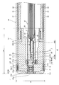
次に、内視鏡2の先端部31の構成について詳細に説明する。図2は、内視鏡2先端の部分断面図である。図2は、内視鏡2の先端部31に設けられた撮像モジュールの基板面に対して直交する面であって撮像モジュールの光軸方向と平行な面で切断した場合の断面図である。図2においては、内視鏡2の挿入部4の先端部31と、湾曲部32の一部を図示する。
Next, the configuration of the distal end portion 31 of the endoscope 2 will be described in detail. FIG. 2 is a partial cross-sectional view of the tip of the endoscope 2. FIG. 2 is a cross-sectional view of the imaging module provided at the distal end portion 31 of the endoscope 2 taken along a plane orthogonal to the substrate surface of the imaging module and parallel to the optical axis direction of the imaging module. In FIG. 2, the distal end portion 31 of the insertion portion 4 of the endoscope 2 and a part of the bending portion 32 are illustrated.
図2に示すように、湾曲部32は、後述する被覆管42内側に配置する湾曲管81内部に挿通された湾曲ワイヤ82の牽引弛緩にともない、上下左右の4方向に湾曲自在である。この湾曲部32の先端側に延設された先端部31内部に、撮像装置36が設けられる。
As shown in FIG. 2, the bending portion 32 is bendable in four directions, up, down, left, and right, along with the pulling and relaxing of the bending wire 82 inserted inside a bending tube 81 disposed inside a cladding tube 42 described later. An imaging device 36 is provided inside the distal end portion 31 extended to the distal end side of the curved portion 32.
撮像装置36は、レンズユニット43と、レンズユニット43の基端側に配置する撮像ユニット35とを有し、接着剤41aで先端部本体41の内側に接着される。先端部本体41は、撮像ユニット35を収容する内部空間を形成するための硬質部材で形成される。先端部本体41の基端外周部は、柔軟な被覆管42によって被覆される。先端部本体41よりも基端側の部材は、湾曲部32が湾曲可能なように、柔軟な部材で構成されている。先端部本体41が配置される先端部31が挿入部4の硬質部分となる。この「硬質部分の長さLaは、挿入部4先端から先端部本体41の基端までとなる。なお、長さLbは、挿入部4先端の外径に対応する。
The imaging device 36 includes a lens unit 43 and an imaging unit 35 disposed on the proximal end side of the lens unit 43, and is adhered to the inside of the tip end main body 41 with an adhesive 41a. The tip portion main body 41 is formed of a hard member for forming an internal space for housing the imaging unit 35. The proximal outer periphery of the tip body 41 is covered by a flexible cladding 42. The member closer to the proximal end than the distal end main body 41 is formed of a flexible member so that the bending portion 32 can be bent. The distal end portion 31 in which the distal end portion main body 41 is disposed is a hard portion of the insertion portion 4. This “hard portion length La” is from the distal end of the insertion portion 4 to the proximal end of the distal end portion main body 41. The length Lb corresponds to the outer diameter of the distal end of the insertion portion 4.
レンズユニット43は、複数の対物レンズ43a-1~43a-4と、対物レンズ43a-1~43a-4を保持するレンズホルダ43bとを有し、このレンズホルダ43bの先端が、先端部本体41内部に挿嵌固定されることによって、先端部本体41に固定される。
The lens unit 43 has a plurality of objective lenses 43a-1 to 43a-4 and a lens holder 43b for holding the objective lenses 43a-1 to 43a-4. The tip of the lens holder 43b is the tip body 41 It is fixed to the tip portion main body 41 by being fixedly fitted inside.
撮像ユニット35は、表面に光を受光する受光面を有する第1チップ44と、伝送バッファを少なくとも有する第2チップ55とによって構成されるCMOSイメージャ45、第1チップ44から延出するフレキシブルプリント基板(FPC基板)46、FPC基板に実装された電子部品56~58、ならびに、第1チップ44の受光面を覆った状態で第1チップ44に接着するガラスリッド49を有する。
The imaging unit 35 includes a CMOS imager 45 including a first chip 44 having a light receiving surface for receiving light on its surface, and a second chip 55 having at least a transmission buffer, and a flexible printed circuit board extending from the first chip 44 (FPC substrate) 46, electronic components 56 to 58 mounted on the FPC substrate, and a glass lid 49 adhered to the first chip 44 in a state of covering the light receiving surface of the first chip 44.
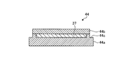
図3に示すように、第1チップ44の受光面側には、複数の画素単位が二次元マトリクス状に配置された受光部37と、電極パッド38が形成され、第1チップ44は、受光部37で光電変換された撮像信号を読み出す読み出し部(図示しない)を備える。また、第1チップ44は、図4に示すように、受光部37を被覆するように基材44a表面に絶縁性のLow-k膜44bを含む配線層が形成されてもよい。Low-k膜は、SiOC、SiOF、または樹脂等からなり、誘電率が低いため、配線層における信号伝送の速度を高めることができるが、水分が浸透しやすく、耐水性(耐湿性)が低いという問題がある。したがって、Low-k膜を形成する場合、第1チップ44内への水分浸入による配線の腐食やLow-k膜の剥離を防止するために、第1チップ44の外周面にステップカット部44cを設けることが好ましい。第1チップ44の外周面にステップカット部44cを設けた場合、図5に示すように、ガラスリッド49と第1チップ44との接続の際に使用する封止樹脂44dを余分に塗布して、ステップカット部44cに封止樹脂44dをはみ出すようにして固定すると、Low-k膜44bを密封することができる。これにより、第1チップ44内への水分の浸入を防止でき、信頼性を向上することができる。Low-k膜44bの密封と、ガラスリッド49と第1チップ44との接続を同時に封止樹脂44dで行なう場合、封止樹脂44dとして、可視光の透過率が高く、透湿度の低い材料を使用することが好ましい。また、Low-k膜44bの密封と、ガラスリッド49と第1チップ44との接続は、別々の工程で別々の材料により行なってもよい。
As shown in FIG. 3, on the light receiving surface side of the first chip 44, a light receiving portion 37 in which a plurality of pixel units are arranged in a two-dimensional matrix, and an electrode pad 38 are formed. A reading unit (not shown) for reading out an imaging signal photoelectrically converted by the unit 37 is provided. Further, as shown in FIG. 4, in the first chip 44, a wiring layer including an insulating Low-k film 44b may be formed on the surface of the base material 44a so as to cover the light receiving section 37. The low-k film is made of SiOC, SiOF, resin or the like and has a low dielectric constant, so the signal transmission speed in the wiring layer can be increased, but water can easily penetrate and the water resistance (moisture resistance) is low. There is a problem of Therefore, when forming the low-k film, the step cut portion 44c is formed on the outer peripheral surface of the first chip 44 in order to prevent corrosion of the wiring due to moisture infiltration into the first chip 44 and peeling of the low-k film. It is preferable to provide. When the step cut portion 44c is provided on the outer peripheral surface of the first chip 44, as shown in FIG. 5, an extra sealing resin 44d used when connecting the glass lid 49 and the first chip 44 is applied. The low-k film 44b can be sealed by fixing the sealing resin 44d to the step-cut portion 44c so as to protrude therefrom. This can prevent the entry of moisture into the first chip 44 and improve the reliability. When sealing of the low-k film 44b and connection between the glass lid 49 and the first chip 44 are simultaneously performed with the sealing resin 44d, a material having high visible light transmittance and low moisture permeability is used as the sealing resin 44d. It is preferred to use. Also, the sealing of the low-k film 44b and the connection between the glass lid 49 and the first chip 44 may be performed using different materials in separate steps.
図3に示したように、第1チップ44の受光部37下部には、電極パッド38が形成される(基材44a表面にLow-k膜44bを形成する場合、電極パッド38下層にはLow-k膜44bが形成される)。電極パッド38は、駆動信号用電極パッド38a-1、電源用電極パッド38a-2および38a-3、グランド用電極パッド38a-4、および画像信号用電極パッド38a-5を含み、駆動信号用電極パッド38a-1と画像信号用電極パッド38a-5とは、最も離間するように配置される。駆動信号用電極パッド38a-1、電源用電極パッド38a-2および38a-3、グランド用電極パッド38a-4、および画像信号用電極パッド38a-5は、それぞれインナーリード39a-1、インナーリード39a-2、インナーリード39a-3、インナーリード39a-4およびインナーリード39a-5と(図8参照)が電気的に接続される。インナーリード39a-1は駆動信号、インナーリード39a-2はグランド信号、インナーリード39a-3およびインナーリード39a-4は電源信号、インナーリード39a-5は画像信号を伝送する。電極パッド38とインナーリード39の接続部は封止樹脂54bによって覆われ、第1チップ44とFPC基板46とが接続される。
As shown in FIG. 3, the electrode pad 38 is formed under the light receiving portion 37 of the first chip 44 (when the Low-k film 44 b is formed on the surface of the base material 44 a -K film 44b is formed). The electrode pad 38 includes a drive signal electrode pad 38a-1, power supply electrode pads 38a-2 and 38a-3, a ground electrode pad 38a-4, and an image signal electrode pad 38a-5, and is a drive signal electrode. The pad 38a-1 and the image signal electrode pad 38a-5 are arranged to be most distant from each other. The drive signal electrode pad 38a-1, the power supply electrode pads 38a-2 and 38a-3, the ground electrode pad 38a-4, and the image signal electrode pad 38a-5 are the inner lead 39a-1 and the inner lead 39a, respectively. The inner lead 39a-3, the inner lead 39a-4 and the inner lead 39a-5 (see FIG. 8) are electrically connected. The inner lead 39a-1 transmits a drive signal, the inner lead 39a-2 transmits a ground signal, the inner lead 39a-3 and the inner lead 39a-4 transmit a power signal, and the inner lead 39a-5 transmits an image signal. The connection portion between the electrode pad 38 and the inner lead 39 is covered with the sealing resin 54 b, and the first chip 44 and the FPC board 46 are connected.
第1チップ44とFPC基板46との接続部は、金属製の補強部材52に覆われる。FPC基板46上の第2チップ55、および電子部品56~58に対する外部静電気の影響を防止するため、補強部材52は、第1チップ44、およびFPC基板46から離間して設置される。
The connection portion between the first chip 44 and the FPC board 46 is covered with a metal reinforcing member 52. In order to prevent the influence of external static electricity on the second chip 55 on the FPC board 46 and the electronic components 56 to 58, the reinforcing member 52 is disposed apart from the first chip 44 and the FPC board 46.
撮像モジュール40は、レンズユニット43および撮像ユニット35とからなる撮像装置36と、第1チップ44を駆動するために第1チップ44と電気的に接続される駆動信号用ケーブル48Aと、第1チップ44から出力される画像信号を伝送する画像出力用信号ケーブル48Bと、第1チップ44、第2チップ55および電子部品56~58に電源を供給する電源用ケーブル48C-1、48C-2と、グランド用信号ケーブル48Dとを備える。
The imaging module 40 includes an imaging device 36 including a lens unit 43 and an imaging unit 35, a drive signal cable 48A electrically connected to the first chip 44 to drive the first chip 44, and the first chip A signal cable for image output 48 B for transmitting an image signal output from the circuit 44, power supply cables 48 C- 1 and 48 C- 2 for supplying power to the first chip 44, the second chip 55 and the electronic components 56 to 58; And a ground signal cable 48D.
駆動信号用ケーブル48A、画像信号用ケーブル48B、電源用ケーブル48C-1、48C-2およびグランド用信号ケーブル48Dの基端は、電気ケーブル束47にまとめられ、挿入部4の基端方向に延伸する。電気ケーブル束47は、挿入部4に挿通配置され、図1に示す操作部5およびユニバーサルコード6を介して、コネクタ7まで延設されている。
The proximal ends of the drive signal cable 48A, the image signal cable 48B, the power supply cables 48C-1 and 48C-2, and the ground signal cable 48D are bundled in the electric cable bundle 47 and extend in the proximal direction of the insertion portion 4 Do. The electric cable bundle 47 is inserted through the insertion portion 4 and extends to the connector 7 via the operation portion 5 and the universal cord 6 shown in FIG.
レンズユニット43の対物レンズ43a-1~43a-4によって結像された被写体像は、対物レンズ43a-1~43a-4の結像位置に配設された第1チップ44によって検出されて、画像信号に変換される。
Subject images formed by the objective lenses 43a-1 to 43a-4 of the lens unit 43 are detected by the first chip 44 disposed at the imaging positions of the objective lenses 43a-1 to 43a-4, It is converted to a signal.
撮像ユニット35および電気ケーブル束47の先端部は、耐性向上のために、熱収縮チューブ50によって外周が被覆される。熱収縮チューブ50内部およびFPC基板46内部は、接着樹脂51によって部品間の隙間が埋められている。
The distal ends of the imaging unit 35 and the electric cable bundle 47 are covered at their outer circumferences by a heat shrinkable tube 50 in order to improve resistance. In the heat-shrinkable tube 50 and the inside of the FPC board 46, a gap between components is filled with an adhesive resin 51.
第1チップホルダ53は、第1チップホルダ53の基端側内周面にガラスリッド49の外周面が嵌め込まれることによって、ガラスリッド49に接着する第1チップ44を保持する。第1チップホルダ53の基端側外周面は、補強部材52の先端側内周面に嵌合する。第1チップホルダ53の先端側内周面には、レンズホルダ43bの基端側外周面が嵌合する。このように各部材同士が嵌合した状態で、レンズホルダ43bの外周面、第1チップホルダ53の外周面、ならびに、熱収縮チューブ50の先端側外周面が、接着剤41aによって先端部本体41の先端の内周面に固定される。
The first chip holder 53 holds the first chip 44 bonded to the glass lid 49 by fitting the outer peripheral surface of the glass lid 49 to the proximal end inner peripheral surface of the first chip holder 53. The proximal end side outer peripheral surface of the first chip holder 53 is fitted to the distal end side inner peripheral surface of the reinforcing member 52. The base end side outer peripheral surface of the lens holder 43 b is fitted to the tip end side inner peripheral surface of the first chip holder 53. Thus, with the respective members fitted, the outer peripheral surface of the lens holder 43b, the outer peripheral surface of the first chip holder 53, and the outer peripheral surface on the tip side of the heat-shrinkable tube 50 use the adhesive 41a to form the tip body 41 It is fixed to the inner peripheral surface of the tip of.
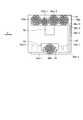
次に、撮像モジュール40について説明する。図6は、図2の撮像モジュールをフレキシブルプリント基板の開口側の側面から平面視した平面図(図7のX矢視)である。図7は、図2の撮像モジュールの後端側から平面視した平面図である。図8は、図2のフレキジブル基板の展開図である。図9は、図2の撮像モジュールを上方から平面視した平面図である。図10は、補強部を形成した場合の撮像モジュールを上方から平面視した平面図である。
Next, the imaging module 40 will be described. 6 is a plan view (viewed in the direction of arrow X in FIG. 7) of the imaging module of FIG. 2 as viewed in plan from the side surface on the opening side of the flexible printed circuit. 7 is a plan view of the imaging module of FIG. 2 viewed in plan from the rear end side. FIG. 8 is a development view of the flexible substrate of FIG. FIG. 9 is a plan view of the imaging module of FIG. 2 as viewed from above. FIG. 10 is a plan view of the image pickup module in the case of forming the reinforcing portion as viewed from above.
FPC基板46は、第1チップ44の電極パッド38から受光面と反対側に延出する第1の領域46a-1と、第1の領域46a-1の幅方向の右側に、第1の領域46a-1に平行して形成される第2の領域46a-2と、第2の領域46a-2の第1の領域46a-1と接する側と反対側に平行して形成される第3の領域46a-3と、を有する。第1の領域46a-1と第2の領域46a-2との間には第1折り曲げ部46b-1が形成されるとともに、第2の領域46a-2と第3の領域46a-3との間に第2折り曲げ部46b-2が形成され、第1折り曲げ部46b-1および第2折り曲げ部46b-2を、各領域が直交するように折り曲げることにより、FPC基板46はコの字状をなしている。第1折り曲げ部46b-1および第2折り曲げ部46b-2は、他の領域より肉薄に形成されるか、または一部にスリットを形成することにより、容易に折り曲げ可能とする。
The FPC board 46 has a first area 46a-1 extending from the electrode pad 38 of the first chip 44 to the opposite side to the light receiving surface, and a first area to the right of the first area 46a-1 in the width direction. A second region 46a-2 formed parallel to 46a-1, and a third region 463 formed parallel to the side opposite to the side in contact with the first region 46a-1 of the second region 46a-2. And a region 46a-3. A first bent portion 46b-1 is formed between the first region 46a-1 and the second region 46a-2, and the second region 46a-2 and the third region 46a-3 The second bent portion 46b-2 is formed between them, and the first bent portion 46b-1 and the second bent portion 46b-2 are bent so that the respective regions are orthogonal to each other, whereby the FPC board 46 has a U-shape. There is no. The first bent portion 46b-1 and the second bent portion 46b-2 can be easily bent by being formed thinner than other regions or by forming a slit in part.
FPC基板46の第1の領域46a-1には、第2チップ55および電子部品56が実装されており、第3の領域46a-3には、電子部品57および58が実装されている。また、第1の領域46a-1の第2チップ55等の実装面には、画像信号用ケーブルを接続する接続ランド63Bが形成され、第3の領域46a-3の電子部品57、58の実装面の裏面側には、駆動信号用ケーブル48A、電源用信号ケーブル48C-1、48C-2、およびグランド用信号ケーブル48Dを接続する接続ランド63A、63C-1、63C-2および63Dが形成されている。
The second chip 55 and the electronic component 56 are mounted on the first region 46a-1 of the FPC board 46, and the electronic components 57 and 58 are mounted on the third region 46a-3. In addition, connection lands 63B for connecting image signal cables are formed on the mounting surface of the first region 46a-1 such as the second chip 55, and the electronic components 57 and 58 of the third region 46a-3 are mounted. On the back side of the surface, connection lands 63A, 63C-1, 63C-2 and 63D for connecting the drive signal cable 48A, the power signal cables 48C-1 and 48C-2, and the ground signal cable 48D are formed. ing.
FPC基板46をコの字状に保持するために、接着樹脂51によってFPC基板46内の隙間が埋められるが、部材を芯としてFPC基板46内に巻き込み、コの字状を保持するようにしてもよい。
In order to hold the FPC board 46 in a U-shape, the gap in the FPC board 46 is filled with the adhesive resin 51, but the member is used as a core to be wound in the FPC board 46 to hold the U-shape. It is also good.
実施の形態1では、画像信号は、第1チップ44の画像信号用電極パッド38a-5から、インナーリード39a-5を介しFPC基板46に伝送され、第1の領域46a-1に実装される第2チップ55に伝送される。画像信号は、伝送バッファを少なくとも有する第2チップ55により増幅された後、第1の領域46a-1上の画像信号用配線パターンおよび画像信号用ケーブル48Bを経由してプロセッサ10に出力される。画像信号用電極パッド38a-5から出力された画像信号は微弱であり、ノイズによる影響を受けやすいが、実施の形態1にかかる撮像モジュール40は、第1チップ44から延出する第1の領域に第2チップ55を実装することにより、最短で微弱な信号を第2チップに出力し増幅できるため、駆動信号のクロストークによる画像ノイズが発生しにくくなる。ノイズの影響を小さくするために、画像信号用配線パターンは直線的(長さが短くなるよう)に形成されることが好ましい。
In the first embodiment, the image signal is transmitted from the image signal electrode pad 38 a-5 of the first chip 44 to the FPC board 46 via the inner lead 39 a-5 and mounted in the first region 46 a-1 It is transmitted to the second chip 55. The image signal is amplified by the second chip 55 having at least a transmission buffer, and then output to the processor 10 via the image signal wiring pattern and the image signal cable 48B on the first region 46a-1. The image signal output from the image signal electrode pad 38 a-5 is weak and susceptible to noise, but the imaging module 40 according to the first embodiment is a first area extending from the first chip 44. By mounting the second chip 55, the shortest and weak signal can be outputted to the second chip and amplified, so that image noise due to the crosstalk of the drive signal is less likely to occur. In order to reduce the influence of noise, it is preferable that the wiring pattern for image signal be formed linearly (in order to shorten the length).
一方、第3の領域46a-3に接続された駆動信号用ケーブル48Aから入力された駆動信号は、主として第3の領域に形成された駆動信号用配線パターンを介して駆動信号用電極パッド38a-1に入力される。駆動信号用配線パターンは、第3の領域46a-3の後端側である駆動信号用ケーブル48Aとの接続部から、第3の領域の前方(第1のチップ44側)に配線され、第3の領域46a-3の前側端部e1から第2チップ55の第1チップ側e2の間の領域Rで、第3の領域46a-3から第2の領域46a-2を介し第1の領域46a-1へと配線されることが好ましい。駆動信号が主として第3の領域46a-3に形成された駆動信号用配線パターンを介して伝送される、すなわち、駆動信号と画像信号とが第2チップ55より第1チップ44側で異なる領域に分離されて伝送されることにより、駆動信号による画像信号へのクロストークの影響を低減することができる。
On the other hand, the drive signal input from the drive signal cable 48A connected to the third area 46a-3 is mainly for the drive signal electrode pad 38a-through the drive signal wiring pattern formed in the third area. It is input to 1. The drive signal wiring pattern is wired from the connection portion with the drive signal cable 48A on the rear end side of the third region 46a-3 to the front (the first chip 44 side) of the third region, and In a region R between the front end e1 of the third region 46a-3 and the first chip side e2 of the second chip 55, a third region 46a-3 to a first region via the second region 46a-2 It is preferable to be wired to 46a-1. The drive signal is mainly transmitted through the drive signal wiring pattern formed in the third region 46a-3, that is, the drive signal and the image signal are different from the second chip 55 to the first chip 44 side. By being separated and transmitted, the influence of the crosstalk on the image signal by the drive signal can be reduced.
撮像モジュール40においては、FPC基板46、第2チップ55、電子部品56~58、駆動信号用ケーブル48A、画像信号用ケーブル48B、電源用ケーブル48C-1、48C-2、グランド用信号ケーブル48Dを含めた撮像モジュール40全体が、第1チップ44を光軸方向に投影した投影領域内に収まるように配置されている。また、図9は、撮像モジュール40を上方から平面視した平面図であるが、図9に示すように、ガラスリッド49の幅方向の一端と、FPC基板46の第2の領域46a-2の一端は、面一に形成されている。ガラスリッド49および/または第1チップ44と、FPC基板46の第2の領域46a-2の幅方向を面一に形成することにより、撮像モジュール40が小型化した場合にも把持が容易となる。さらに、図10に示すように、面一とした面に、接着剤により板状の補強部59を接合しても良い。補強部59の形成により、把持が容易となるとともに、補強部59を接合する接着剤により、ガラスリッド49、第1チップ44およびFPC基板46間の接続強度も向上することができる。
In the imaging module 40, the FPC board 46, the second chip 55, the electronic components 56 to 58, the drive signal cable 48A, the image signal cable 48B, the power supply cables 48C-1 and 48C-2, and the ground signal cable 48D The entire imaging module 40 included is disposed so as to fall within the projection area obtained by projecting the first chip 44 in the optical axis direction. 9 is a plan view of the imaging module 40 in plan view from above, but as shown in FIG. 9, one end of the glass lid 49 in the width direction and the second region 46a-2 of the FPC board 46 are shown. One end is formed flush. By forming the glass lid 49 and / or the first chip 44 and the width direction of the second region 46a-2 of the FPC board 46 flush, gripping becomes easy even when the imaging module 40 is miniaturized. . Furthermore, as shown in FIG. 10, a plate-like reinforcing portion 59 may be joined to the flush surface by an adhesive. The formation of the reinforcing portion 59 facilitates gripping, and the adhesive for bonding the reinforcing portion 59 can also improve the connection strength between the glass lid 49, the first chip 44, and the FPC board 46.
実施の形態1では、駆動信号用電極パッド38a-1と画像信号用電極パッド38a-5が最も離間するように形成されるとともに、第1の領域46a-1の駆動信号用電極パッド38a-1側に、駆動信号用ケーブル48Aが接続される第3の領域46a-3が形成されるため、駆動信号用配線パターンは画像信号用配線パターンと交差することがなく、駆動信号による画像信号へのクロストークを低減することができる。
In the first embodiment, the drive signal electrode pad 38a-1 and the image signal electrode pad 38a-5 are formed to be most separated from each other, and the drive signal electrode pad 38a-1 of the first region 46a-1 is formed. Since the third region 46a-3 to which the drive signal cable 48A is connected is formed on the side, the drive signal wiring pattern does not cross the image signal wiring pattern, and an image signal is generated by the drive signal. Cross talk can be reduced.
実施の形態1では、駆動信号用ケーブル48A、電源用ケーブル48C-1および48C-2、グランド用信号ケーブル48Dが、第3の領域46a-3の外側面(電子部品57および58の実装面の裏面側)に接続されているが、第3の領域46a-3の内側面(電子部品57および58の実装面と同一面)に実装されていてもよい。また、撮像モジュール40全体が、第1チップ44を光軸方向に投影した投影領域内に収まるように配置されていれば、画像出力用信号ケーブル48Bが、第1の領域46a-1の外側面(第2チップ55の実装面と反対側)に接続されていても良い。駆動信号や画像出力用信号が複数ある場合でも、同様に第1の領域、第3の領域にて接続すれば良い。
In the first embodiment, drive signal cable 48A, power supply cables 48C-1 and 48C-2, and ground signal cable 48D are the outer surfaces of third region 46a-3 (the mounting surfaces of electronic components 57 and 58). Although it is connected to the back surface side, it may be mounted on the inner surface (the same surface as the mounting surface of the electronic components 57 and 58) of the third region 46a-3. In addition, when the entire imaging module 40 is disposed so as to fall within the projection area obtained by projecting the first chip 44 in the optical axis direction, the image output signal cable 48B is the outer surface of the first area 46a-1. (The side opposite to the mounting surface of the second chip 55) may be connected. Even when there are a plurality of drive signals and image output signals, they may be similarly connected in the first area and the third area.
(実施の形態2)
実施の形態2にかかる撮像モジュールは、FPC基板46がU字状をなし、第1の領域46a-1の幅方向の端面(右側)に平行して形成される第2の領域46a-2に駆動信号用ケーブル48Aが接続される点で実施の形態1と異なる。 Second Embodiment
In the imaging module according to the second embodiment, thesecond area 46a-2 formed in parallel with the end face (right side) of the first area 46a-1 in the width direction of the FPC board 46 has a U shape. This embodiment differs from the first embodiment in that the drive signal cable 48A is connected.
実施の形態2にかかる撮像モジュールは、FPC基板46がU字状をなし、第1の領域46a-1の幅方向の端面(右側)に平行して形成される第2の領域46a-2に駆動信号用ケーブル48Aが接続される点で実施の形態1と異なる。 Second Embodiment
In the imaging module according to the second embodiment, the
図11は、実施の形態2にかかる撮像モジュールをフレキシブルプリント基板面に対して鉛直、かつ、撮像モジュールの光軸方向と平行な面で切断した場合の断面図である。図12は、図11の撮像モジュールの後端側から平面視した平面図である。なお、図12において、第1チップ44の図示は省略している。
FIG. 11 is a cross-sectional view of the imaging module according to the second embodiment taken along a plane perpendicular to the surface of the flexible printed circuit and parallel to the optical axis direction of the imaging module. 12 is a plan view of the imaging module of FIG. 11 viewed in plan from the rear end side. In FIG. 12, the first chip 44 is not shown.
実施の形態2にかかる撮像モジュール40Aにおいて、フレキシブルプリント基板46は、第1チップ44の電極パッド38から延出する第1の領域46a-1と、第1の領域46a-1の右側に平行して形成される第2の領域46a-2と、第1の領域46a-1の左側に平行して形成される第3の領域46a-3と、を有し、第1の領域46a-1と第2の領域46a-2、および第1の領域46a-1と第3の領域46a-3との間には、それぞれ第1折り曲げ部46b-1および第2折り曲げ部46b-2が形成される。第1折り曲げ部46b-1および第2折り曲げ部46b-2を、各領域が直交するように折り曲げることにより、FPC基板46はU字状をなす。
In the imaging module 40A according to the second embodiment, the flexible printed circuit 46 is parallel to the first region 46a-1 extending from the electrode pad 38 of the first chip 44 and to the right of the first region 46a-1. And a third region 46a-3 formed in parallel on the left side of the first region 46a-1, and the first region 46a-1 and A first bent portion 46b-1 and a second bent portion 46b-2 are formed between the second region 46a-2 and the first region 46a-1 and the third region 46a-3, respectively. . The FPC board 46 has a U shape by bending the first bent portion 46b-1 and the second bent portion 46b-2 so that the respective regions are orthogonal to each other.
実施の形態2は、FPC基板46の第1の領域46a-1に第2チップ55および電子部品56が実装され、第2の領域46a-2に電子部品57および58が実装されている。また、FPC基板46の第1の領域46a-1の外側面(第2チップ55の実装面の裏面側)に画像信号用ケーブル48Bが接続され、第2の領域46a-2の外側面(電子部品57および58の実装面の裏面側)に、駆動信号用ケーブル48Aとグランド用信号ケーブル48Dが接続され、第3の領域46a-3の外側面に電源用信号ケーブル48C-1、48C-2が接続されている。
In the second embodiment, the second chip 55 and the electronic component 56 are mounted on the first region 46a-1 of the FPC board 46, and the electronic components 57 and 58 are mounted on the second region 46a-2. The image signal cable 48B is connected to the outer surface of the first area 46a-1 of the FPC board 46 (the back surface side of the mounting surface of the second chip 55), and the outer surface of the second area 46a-2 (electrons The drive signal cable 48A and the ground signal cable 48D are connected to the rear surface side of the mounting surface of the components 57 and 58, and the power supply signal cables 48C-1 and 48C-2 are connected to the outer surface of the third region 46a-3. Is connected.
画像信号は、実施の形態1と同様に、第1チップ44の画像信号用電極パッド38a-5から、インナーリード39a-5を介しFPC基板46に伝送され、第1の領域46a-1に実装される第2チップ55に伝送される。画像信号は、第2チップ55により増幅された後、第1の領域46a-1上の画像信号用配線パターンおよび画像信号用ケーブル48Bを経由してプロセッサ10に出力される。
As in the first embodiment, the image signal is transmitted from the image signal electrode pad 38a-5 of the first chip 44 to the FPC board 46 through the inner lead 39a-5 and mounted in the first region 46a-1. Is transmitted to the second chip 55. The image signal is amplified by the second chip 55, and then output to the processor 10 via the image signal wiring pattern on the first area 46a-1 and the image signal cable 48B.
一方、第2の領域46a-2に接続された駆動信号用ケーブル48Aから入力された駆動信号は、主として第2の領域46a-2に形成された駆動信号用配線パターンを介して駆動信号用電極パッド38a-1に入力される。駆動信号用配線パターンは、第2の領域46a-2の後端側である駆動信号用ケーブル48Aとの接続部から、第2の領域の前方(第1のチップ44側)に配線され、第2の領域46a-1の前側端部e3から第2チップ55の第1チップ44側面位置e2の間の領域R1で、第2の領域46a-2から領域46a-1へと配線されることが好ましい。実施の形態2では、駆動信号が主として第2の領域に形成された駆動信号用配線パターンを介して伝送される、すなわち、駆動信号と画像信号とが第2チップ55より第1チップ44側で異なる領域に分離されて伝送されることにより、駆動信号による画像信号へのクロストークの影響を低減することができる。
On the other hand, the drive signal input from the drive signal cable 48A connected to the second area 46a-2 is mainly for the drive signal electrode through the drive signal wiring pattern formed in the second area 46a-2. The data is input to the pad 38a-1. The drive signal wiring pattern is wired from the connection portion with the drive signal cable 48A on the rear end side of the second region 46a-2 to the front (the first chip 44 side) of the second region, and Wiring from the second region 46a-2 to the region 46a-1 in the region R1 between the front end e3 of the second region 46a-1 and the side surface position e2 of the first chip 44 of the second chip 55 preferable. In the second embodiment, the drive signal is mainly transmitted through the drive signal wiring pattern formed in the second region, that is, the drive signal and the image signal are closer to the first chip 44 than the second chip 55. By being separated and transmitted to different regions, the influence of the crosstalk on the image signal by the drive signal can be reduced.
また、実施の形態2においても、実施の形態1と同様に駆動信号用電極パッド38a-1と画像信号用電極パッド38a-5が最も離間するように形成されるとともに、第1の領域46a-1の駆動信号用電極パッド38a-1側に、駆動信号用ケーブル48Aが接続される第2の領域46a-2が形成されるため、駆動信号用配線パターンは画像信号用配線パターンと交差することがなく、駆動信号による画像信号へのクロストークを低減することができる。
Also in the second embodiment, as in the first embodiment, the drive signal electrode pad 38a-1 and the image signal electrode pad 38a-5 are formed to be most separated from each other, and the first region 46a-is formed. Because the second region 46a-2 to which the drive signal cable 48A is connected is formed on the side of the drive signal electrode pad 38a-1 of 1, the drive signal wiring pattern intersects the image signal wiring pattern. And the crosstalk to the image signal by the drive signal can be reduced.
(実施の形態3)
実施の形態3にかかる撮像モジュールは、FPC基板46がL字状をなし、第1の領域46a-1の幅方向の端面に平行して形成される第2の領域46a-2に駆動信号用ケーブル48Aが接続される点で実施の形態1と異なる。図13は、実施の形態3にかかる撮像モジュールの後端側から平面視した平面図である。なお、図13において、第1チップ44の図示は省略している。 Third Embodiment
In the imaging module according to the third embodiment, thesecond region 46a-2 formed in parallel with the end face of the first region 46a-1 in the width direction of the FPC board 46 has an L shape and is used for driving signals. This embodiment differs from the first embodiment in that the cable 48A is connected. FIG. 13 is a plan view of the imaging module according to the third embodiment viewed in plan from the rear end side. The first chip 44 is not shown in FIG.
実施の形態3にかかる撮像モジュールは、FPC基板46がL字状をなし、第1の領域46a-1の幅方向の端面に平行して形成される第2の領域46a-2に駆動信号用ケーブル48Aが接続される点で実施の形態1と異なる。図13は、実施の形態3にかかる撮像モジュールの後端側から平面視した平面図である。なお、図13において、第1チップ44の図示は省略している。 Third Embodiment
In the imaging module according to the third embodiment, the
実施の形態3にかかる撮像モジュール40Bにおいて、フレキシブルプリント基板46は、第1チップ44の電極パッド38から延出する第1の領域46a-1と、第1の領域46a-1の右側に平行して形成される第2の領域46a-2と、を有し、第1の領域46a-1と第2の領域46a-2との間の折り曲げ部46b-1を、第1の領域46a-1と第2の領域46a-2とが直交するように折り曲げられている。
In the imaging module 40B according to the third embodiment, the flexible printed circuit 46 is parallel to the first area 46a-1 extending from the electrode pad 38 of the first chip 44 and to the right of the first area 46a-1. And a second region 46a-2 formed in the first region 46a-1 and a bent portion 46b-1 between the first region 46a-1 and the second region 46a-2; And the second region 46a-2 are bent at right angles.
実施の形態3では、FPC基板46の第1の領域46a-1に第2チップ55および電子部品56が実装され、第2の領域46a-2に電子部品57および58が実装されている。また、FPC基板46の第1の領域46a-1の内側面(第2チップ55の実装面)に画像信号用ケーブル48Bが接続され、第2の領域46a-2の外側面(電子部品57および58の実装面の裏面側)に、駆動信号用ケーブル48Aとグランド用信号ケーブル48Dが接続され、第2の領域46a-2の内側面に電源用信号ケーブル48C-1、48C-2が接続されている。
In the third embodiment, the second chip 55 and the electronic component 56 are mounted on the first region 46a-1 of the FPC board 46, and the electronic components 57 and 58 are mounted on the second region 46a-2. The image signal cable 48B is connected to the inner side surface (the mounting surface of the second chip 55) of the first region 46a-1 of the FPC board 46, and the outer surface (the electronic component 57 and the electronic component 57 of the second region 46a-2). The drive signal cable 48A and the ground signal cable 48D are connected to the back surface side of the mounting surface 58, and the power supply signal cables 48C-1 and 48C-2 are connected to the inner side surface of the second region 46a-2. ing.
画像信号は、実施の形態1と同様に、第1チップ44の画像信号用電極パッド38a-5から、インナーリード39a-5を介しFPC基板46に伝送され、第1の領域46a-1に実装される第2チップ55に伝送される。画像信号は、第2チップ55により増幅された後、第1の領域46a-1上の画像信号用配線パターンおよび画像信号用ケーブル48Bを経由してプロセッサ10に出力される。一方、第2の領域46a-2に接続された駆動信号用ケーブル48Aから入力された駆動信号は、実施の形態2と同様に、主として第2の領域46a-2に形成された駆動信号用配線パターンを介して駆動信号用電極パッド38a-1に入力される。駆動信号用配線パターンは、第2の領域46a-2の後端側である駆動信号用ケーブル48Aとの接続部から、第2の領域46a-2の前方(第1のチップ44側)に配線され、第2の領域46a-1の前側端部から第2チップ55の第1チップ側面位置の間の領域で、第2の領域46a-2から領域46a-1へと配線されることが好ましい。実施の形態3では、駆動信号が主として第2の領域に形成された駆動信号用配線パターンを介して伝送される、すなわち、駆動信号と画像信号とが第2チップ55より第1チップ44側で異なる領域に分離されて伝送されることにより、駆動信号による画像信号へのクロストークの影響を低減することができる。
As in the first embodiment, the image signal is transmitted from the image signal electrode pad 38a-5 of the first chip 44 to the FPC board 46 through the inner lead 39a-5 and mounted in the first region 46a-1. Is transmitted to the second chip 55. The image signal is amplified by the second chip 55, and then output to the processor 10 via the image signal wiring pattern on the first area 46a-1 and the image signal cable 48B. On the other hand, as with the second embodiment, the drive signal input from the drive signal cable 48A connected to the second area 46a-2 is mainly the drive signal wiring formed in the second area 46a-2. The signal is input to the drive signal electrode pad 38a-1 through the pattern. The drive signal wiring pattern is wired from the connection portion with the drive signal cable 48A which is the rear end side of the second region 46a-2 to the front (the first chip 44 side) of the second region 46a-2. Are preferably wired from the second area 46a-2 to the area 46a-1 in the area between the front end of the second area 46a-1 and the first chip side surface position of the second chip 55. . In the third embodiment, the drive signal is mainly transmitted through the drive signal wiring pattern formed in the second region, that is, the drive signal and the image signal are closer to the first chip 44 than the second chip 55. By being separated and transmitted to different regions, the influence of the crosstalk on the image signal by the drive signal can be reduced.
また、実施の形態3においても、実施の形態1と同様に駆動信号用電極パッド38a-1と画像信号用電極パッド38a-5が最も離間するように形成されるとともに、第1の領域46a-1の駆動信号用電極パッド38a-1側に、駆動信号用ケーブル48Aが接続される第2の領域46a-2が形成されるため、駆動信号用配線パターンは画像信号用配線パターンと交差することがなく、画像信号への影響を低減することができる。
Also in the third embodiment, as in the first embodiment, the drive signal electrode pad 38a-1 and the image signal electrode pad 38a-5 are formed to be most separated from each other, and the first region 46a-is formed. Because the second region 46a-2 to which the drive signal cable 48A is connected is formed on the side of the drive signal electrode pad 38a-1 of 1, the drive signal wiring pattern intersects the image signal wiring pattern. And the influence on the image signal can be reduced.
(実施の形態4)
実施の形態3にかかる撮像モジュールは、FPC基板46が5つの領域を有し、画像信号用ケーブル48Bが接続される第1の領域46a-1と最も離間した第5の領域46a-5に駆動信号用ケーブル48Aが接続される点で実施の形態1と異なる。図14は、実施の形態4にかかる撮像モジュールの後端側から平面視した平面図である。なお、図14において、第1チップ44の図示は省略している。Embodiment 4
In the imaging module according to the third embodiment, theFPC board 46 has five areas, and is driven to the fifth area 46 a-5 that is most distant from the first area 46 a-1 to which the image signal cable 48 B is connected. This embodiment differs from the first embodiment in that the signal cable 48A is connected. FIG. 14 is a plan view of the imaging module according to the fourth embodiment viewed in plan from the rear end side. In FIG. 14, the first chip 44 is not shown.
実施の形態3にかかる撮像モジュールは、FPC基板46が5つの領域を有し、画像信号用ケーブル48Bが接続される第1の領域46a-1と最も離間した第5の領域46a-5に駆動信号用ケーブル48Aが接続される点で実施の形態1と異なる。図14は、実施の形態4にかかる撮像モジュールの後端側から平面視した平面図である。なお、図14において、第1チップ44の図示は省略している。
In the imaging module according to the third embodiment, the
実施の形態4にかかる撮像モジュール40Cにおいて、フレキシブルプリント基板46は、第1チップ44の電極パッド38から延出する第1の領域46a-1と、第1の領域46a-1の右側に、第1の領域46a-1に平行して形成される第2の領域46a-2と、第2の領域46a-2の第1の領域46a-1と接する側と反対側に平行して形成される第3の領域46a-3と、第3の領域46a-3の第2の領域46a-2と接する側と反対側に平行して形成される第4の領域46a-4と、第4の領域46a-4の第3の領域46a-3と接する側と反対側に平行して形成される第5の領域46a-5と、を有する。第1の領域46a-1と第2の領域46a-2との間、第2の領域46a-2と第3の領域46a-3との間、第3の領域46a-3と第4の領域46a-4との間、および第4の領域46a-4と第5の領域46a-5との間には、それぞれ折り曲げ部が形成され、各折り曲げ部を折り曲げることにより、FPC基板46は略円弧状をなしている。
In the imaging module 40C according to the fourth embodiment, the flexible printed circuit board 46 has a first area 46a-1 extending from the electrode pad 38 of the first chip 44 and a first area 46a-1 on the right side. The second region 46a-2 formed in parallel to the first region 46a-1 and the second region 46a-2 formed in parallel to the side opposite to the side in contact with the first region 46a-1 A third region 46a-3 and a fourth region 46a-4 formed in parallel with the side opposite to the side in contact with the second region 46a-2 of the third region 46a-3, and a fourth region And a fifth region 46a-5 formed in parallel to the side opposite to the side in contact with the third region 46a-3 of 46a-4. Between the first area 46a-1 and the second area 46a-2, between the second area 46a-2 and the third area 46a-3, the third area 46a-3 and the fourth area Bent portions are formed between the fourth region 46 a-4 and the fifth region 46 a-5, and the FPC board 46 is substantially circular by bending the respective bending portions. It has an arc shape.
実施の形態4では、FPC基板46の第1の領域46a-1に第2チップ55および電子部品56が実装され、第5の領域46a-5に電子部品57および58が実装されている。また、FPC基板46の第1の領域46a-1の内側面(第2チップ55の実装面)に画像信号用ケーブル48B、第5の領域46a-5の内側面(電子部品57および58の実装面)に駆動信号用ケーブル48A、第2の領域46a-2の内側面にグランド用信号ケーブル48D、第3の領域46a-3の内側面に電源用信号ケーブル48C-2、第4の領域46a-4の内側面に電源用信号ケーブル48C-1が接続されている。
In the fourth embodiment, the second chip 55 and the electronic component 56 are mounted on the first region 46a-1 of the FPC board 46, and the electronic components 57 and 58 are mounted on the fifth region 46a-5. The image signal cable 48B is mounted on the inner surface (the mounting surface of the second chip 55) of the first area 46a-1 of the FPC board 46, and the inner surface (the electronic components 57 and 58) of the fifth area 46a-5. Side), the drive signal cable 48A, the inner side surface of the second area 46a-2, the signal cable for ground 48D, the inner side surface of the third area 46a-3, the signal cable for power supply 48C-2, the fourth area 46a The power supply signal cable 48C-1 is connected to the inner side surface of the -4.
画像信号は、実施の形態1と同様に、第1チップ44の画像信号用電極パッド38a-5から、インナーリード39a-5を介しFPC基板46に伝送され、第1の領域46a-1に実装される第2チップ55に伝送される。画像信号は、第2チップ55により増幅された後、第1の領域46a-1上の画像信号用配線パターンおよび画像信号用ケーブル48Bを経由してプロセッサ10に出力される。一方、第5の領域46a-5に接続された駆動信号用ケーブル48Aから入力された駆動信号は、主として第5の領域に形成された駆動信号用配線パターンを介して駆動信号用電極パッド38a-1に入力される。駆動信号用配線パターンは、第5の領域46a-5の後端側である駆動信号用ケーブル48Aとの接続部から、第5の領域46a-5の前方(第1のチップ44側)に配線され、第5の領域46a-5の前側端部から、第2チップ55の第1チップ側面位置の間の領域で、第4の領域46a-4、第3の領域46a-3、および第2の領域46a-2を介し第1の領域46a-1へと配線される。実施の形態4では、駆動信号が主として第5の領域に形成された駆動信号用配線パターンを介して伝送される、すなわち、駆動信号と画像信号とが第2チップ55より第1チップ44側で異なる領域に分離されて伝送されることにより、駆動信号による画像信号へのクロストークの影響を低減することができる。
As in the first embodiment, the image signal is transmitted from the image signal electrode pad 38a-5 of the first chip 44 to the FPC board 46 through the inner lead 39a-5 and mounted in the first region 46a-1. Is transmitted to the second chip 55. The image signal is amplified by the second chip 55, and then output to the processor 10 via the image signal wiring pattern on the first area 46a-1 and the image signal cable 48B. On the other hand, the drive signal input from the drive signal cable 48A connected to the fifth area 46a-5 is mainly for the drive signal electrode pad 38a-via the drive signal wiring pattern formed in the fifth area. It is input to 1. The drive signal wiring pattern is wired from the connection portion with the drive signal cable 48A on the rear end side of the fifth region 46a-5 to the front (first chip 44 side) of the fifth region 46a-5. A fourth region 46a-4, a third region 46a-3, and a second region between the front end of the fifth region 46a-5 and the first chip side surface position of the second chip 55. Wiring to the first region 46a-1 via the region 46a-2. In the fourth embodiment, the drive signal is mainly transmitted through the drive signal wiring pattern formed in the fifth region, that is, the drive signal and the image signal are closer to the first chip 44 than the second chip 55. By being separated and transmitted to different regions, the influence of the crosstalk on the image signal by the drive signal can be reduced.
また、実施の形態4においても、実施の形態1と同様に駆動信号用電極パッド38a-1と画像信号用電極パッド38a-5が最も離間するように形成されるとともに、第1の領域46a-1の駆動信号用電極パッド38a-1側に、駆動信号用ケーブル48Aが接続される第5の領域46a-5が形成されるため、駆動信号用配線パターンは画像信号用配線パターンと交差することがなく、画像信号への影響を低減することができる。
Also in the fourth embodiment, as in the first embodiment, the drive signal electrode pad 38a-1 and the image signal electrode pad 38a-5 are formed to be most separated from each other, and the first region 46a-is formed. Since the fifth region 46a-5 to which the drive signal cable 48A is connected is formed on the side of the drive signal electrode pad 38a-1 of 1, the drive signal wiring pattern intersects the image signal wiring pattern. And the influence on the image signal can be reduced.
1 内視鏡装置
2 内視鏡
4 挿入部
5 操作部
6 ユニバーサルコード
7 コネクタ
9 光源装置
10 プロセッサ
13 表示装置
17 処置具挿入口
31 先端部
32 湾曲部
33 可撓管部
35 撮像ユニット
36 撮像装置
37 受光部
38 電極パッド
38a-1 駆動信号用電極パッド
38a-2、38a-3 電源信号用電極パッド
38a-4 グランド用電極パッド
38a-5 画像信号用電極パッド
39、39a-1~39a-5 インナーリード
40、40A、40B、40C 撮像モジュール
41 先端部本体
41a 接着剤
42 被覆管
43 レンズユニット
43a-1~43a-4 対物レンズ
43b レンズホルダ
44 第1チップ
44a 基材
44b Low-k膜
44c ステップカット部
44d 封止樹脂
45 CMOSイメージャ
46 フレキシブルプリント基板
46a-1 第1の領域
46a-2 第2の領域
46a-3 第3の領域
46b-1 第1折り曲げ部
46b-2 第2折り曲げ部
47 電気ケーブル束
48A 駆動信号用ケーブル
48B 画像信号用ケーブル
48C-1、48C-2 電源用ケーブル
48D グランド用信号ケーブル
49 ガラスリッド
50 熱収縮チューブ
51 接着樹脂
52 補強部材
53 第1チップホルダ
54b 封止樹脂
55 第2チップ
56~58 電子部品
59 補強部
81 湾曲管
82 湾曲ワイヤ DESCRIPTION OFSYMBOLS 1 endoscope apparatus 2 endoscope 4 insertion part 5 operation part 6 universal cord 7 connector 9 light source device 10 processor 13 display apparatus 17 treatment tool insertion port 31 tip part 32 curved part 33 flexible tube part 35 imaging unit 36 imaging device 37 light receiving unit 38 electrode pad 38a-1 electrode pad for driving signal 38a-2, 38a-3 electrode pad for power signal 38a-4 electrode pad for ground 38a-5 electrode pad for image signal 39, 39a-1 to 39a-5 Inner lead 40, 40A, 40B, 40C Imaging module 41 Tip body 41a Adhesive 42 Coated tube 43 Lens unit 43a-1 to 43a-4 Objective lens 43b Lens holder 44 1st chip 44a Base 44b Low-k film 44c Step Cut part 44d sealing resin 45 CMOS image 46 flexible printed circuit board 46a-1 first area 46a-2 second area 46a-3 third area 46b-1 first bent portion 46b-2 second bent portion 47 electric cable bundle 48A drive signal cable 48B image Signal cable 48C-1 and 48C-2 Power supply cable 48D Signal cable for ground 49 Glass lid 50 Heat-shrinkable tube 51 Adhesive resin 52 Reinforcement member 53 First chip holder 54b Sealing resin 55 Second chip 56 to 58 Electronic parts 59 Reinforcement 81 Curved tube 82 Curved wire
2 内視鏡
4 挿入部
5 操作部
6 ユニバーサルコード
7 コネクタ
9 光源装置
10 プロセッサ
13 表示装置
17 処置具挿入口
31 先端部
32 湾曲部
33 可撓管部
35 撮像ユニット
36 撮像装置
37 受光部
38 電極パッド
38a-1 駆動信号用電極パッド
38a-2、38a-3 電源信号用電極パッド
38a-4 グランド用電極パッド
38a-5 画像信号用電極パッド
39、39a-1~39a-5 インナーリード
40、40A、40B、40C 撮像モジュール
41 先端部本体
41a 接着剤
42 被覆管
43 レンズユニット
43a-1~43a-4 対物レンズ
43b レンズホルダ
44 第1チップ
44a 基材
44b Low-k膜
44c ステップカット部
44d 封止樹脂
45 CMOSイメージャ
46 フレキシブルプリント基板
46a-1 第1の領域
46a-2 第2の領域
46a-3 第3の領域
46b-1 第1折り曲げ部
46b-2 第2折り曲げ部
47 電気ケーブル束
48A 駆動信号用ケーブル
48B 画像信号用ケーブル
48C-1、48C-2 電源用ケーブル
48D グランド用信号ケーブル
49 ガラスリッド
50 熱収縮チューブ
51 接着樹脂
52 補強部材
53 第1チップホルダ
54b 封止樹脂
55 第2チップ
56~58 電子部品
59 補強部
81 湾曲管
82 湾曲ワイヤ DESCRIPTION OF
Claims (11)
- 受光量に応じた撮像信号を生成して出力する複数の画素が二次元マトリクス状に配置される受光部、および、前記撮像信号を読み出すために前記複数の画素から選択対象の画素を選択する読み出し部を少なくとも有する第1チップと、
前記第1チップの電極パッドに一端から延出するインナーリードにより接続されたフレキシブルプリント基板と、
前記フレキシブルプリント基板に実装された伝送バッファを少なくとも有する第2チップと、
前記フレキシブルプリント基板の他端に接続された、画像信号が出力される画像信用号ケーブル、および駆動信号を入力する駆動信号用ケーブルを含む信号ケーブルと、
を備えた撮像モジュールにおいて、
前記第1チップと前記第2チップとによりCMOS撮像素子が構成され、前記第1チップから出力された画像信号は前記第2チップで増幅され、
前記フレキシブルプリント基板は、前記撮像モジュールの光軸方向に平行な少なくとも1つの折り曲げ部により折り曲げられて区分けされた2以上の領域を備えるとともに、前記第2チップと前記駆動信号用ケーブルは、前記フレキシブルプリント基板の異なる領域にそれぞれ接続されることを特徴とする撮像モジュール。 A light receiving unit in which a plurality of pixels that generate and output imaging signals according to the amount of received light are arranged in a two-dimensional matrix, and reading for selecting pixels to be selected from the plurality of pixels in order to read out the imaging signals A first chip having at least a portion;
A flexible printed circuit board connected to the electrode pad of the first chip by an inner lead extending from one end;
A second chip having at least a transmission buffer mounted on the flexible printed circuit board;
A signal cable connected to the other end of the flexible printed circuit, the image signal cable for outputting an image signal, and a signal cable including a drive signal cable for inputting a drive signal;
In the imaging module provided with
A CMOS imaging device is configured by the first chip and the second chip, and an image signal output from the first chip is amplified by the second chip,
The flexible printed circuit board includes two or more areas which are bent and divided by at least one bending portion parallel to the optical axis direction of the imaging module, and the second chip and the drive signal cable are flexible. An imaging module characterized by being respectively connected to different areas of a printed circuit board. - 前記フレキシブルプリント基板は、前記第1チップの電極パッドから延出する第1の領域と、前記第1の領域の幅方向の端面のいずれか一方に平行して形成される第2の領域とを有し、前記第1の領域と前記第2の領域との間に形成される前記折り曲げ部で、前記第1の領域と前記第2の領域とが直交するように折り曲げられ、
前記第2チップおよび前記画像信号用ケーブルは前記第1の領域、前記駆動信号用ケーブルは前記第2の領域にそれぞれ接続されることを特徴とする請求項1に記載の撮像モジュール。 The flexible printed circuit board has a first area extending from the electrode pad of the first chip and a second area formed parallel to one of the end faces in the width direction of the first area. And at the bent portion formed between the first region and the second region, the first region and the second region are bent so as to be orthogonal to each other.
The imaging module according to claim 1, wherein the second chip and the image signal cable are connected to the first area, and the drive signal cable is connected to the second area. - 前記駆動信号を伝送する駆動信号用配線パターンは、前記第2の領域の前記第1チップ側端面と前記第2チップの間で前記第2の領域から前記第1の領域へと配線されることを特徴とする請求項2に記載の撮像モジュール。 The drive signal wiring pattern for transmitting the drive signal is wired from the second area to the first area between the first chip side end surface of the second area and the second chip. The imaging module according to claim 2, characterized in that
- 前記フレキシブルプリント基板は、前記第1のチップの電極パッドから延出する第1の領域と、前記第1の領域の幅方向の端面のいずれか一方に平行して形成される第2の領域と、前記第2の領域の第1の領域と接する側と反対側に平行して形成される第3の領域とを有し、前記第1の領域と前記第2の領域、および前記第2の領域と前記第3の領域との間に形成される前記折り曲げ部で各領域が直交するように折り曲げられるとともに、
前記第2チップおよび前記画像信号用ケーブルは前記第1の領域、前記駆動信号用ケーブルは前記第3の領域にそれぞれ接続されることを特徴とする請求項1に記載の撮像モジュール。 The flexible printed circuit board has a first area extending from the electrode pad of the first chip and a second area formed parallel to one of the end faces in the width direction of the first area. And a third region formed in parallel with the side in contact with the first region and the opposite side of the second region, the first region, the second region, and the second region. The respective regions are bent so as to be orthogonal to each other at the bending portion formed between the region and the third region, and
The imaging module according to claim 1, wherein the second chip and the image signal cable are connected to the first area, and the drive signal cable is connected to the third area. - 前記駆動信号を伝送する駆動信号用配線パターンは、前記第3の領域の前記第1チップ側端面と前記第2チップの間で、前記第3の領域から前記第1の領域へと配線されることを特徴とする請求項4に記載の撮像モジュール。 The drive signal wiring pattern for transmitting the drive signal is wired from the third area to the first area between the first chip side end face of the third area and the second chip. The imaging module according to claim 4, characterized in that:
- 前記フレキシブルプリント基板は、前記第1のチップの電極パッドから延出する第1の領域と、前記第1の領域の幅方向の端面のいずれか一方に平行して形成される第2の領域と、前記第1の領域の幅方向の他の端面に平行して形成される第3の領域とを有し、前記第1の領域と前記第2の領域、および前記第1の領域と前記第3の領域との間に形成される前記折り曲げ部で、各領域が直交するように折り曲げられるとともに、
前記第2チップおよび前記画像信号用ケーブルは前記第1の領域、前記駆動信号用ケーブルは前記第2の領域または前記第3の領域にそれぞれ接続されることを特徴とする請求項1に記載の撮像モジュール。 The flexible printed circuit board has a first area extending from the electrode pad of the first chip and a second area formed parallel to one of the end faces in the width direction of the first area. And a third area formed in parallel to the other end face in the width direction of the first area, the first area and the second area, and the first area and the first area. At the folds formed between the three regions, the regions are folded orthogonally, and
2. The device according to claim 1, wherein the second chip and the image signal cable are connected to the first area, and the drive signal cable is connected to the second area or the third area. Imaging module. - 前記駆動信号を伝送する駆動信号用配線パターンは、前記駆動信号用ケーブルが接続される前記第2の領域または前記第3の領域の、前記第1チップ側端面と前記第2チップの間で、前記第2の領域または前記第3の領域から前記第1の領域へと配線されることを特徴とする請求項6に記載の撮像モジュール。 The drive signal wiring pattern for transmitting the drive signal is formed between the first chip side end face and the second chip in the second area or the third area to which the drive signal cable is connected. 7. The imaging module according to claim 6, wherein the wiring is performed from the second area or the third area to the first area.
- 前記フレキシブルプリント基板は、前記第1のチップの電極パッドから延出する第1の領域と、前記第1の領域の幅方向の端面に平行して形成される3以上の領域とを有し、各領域の間に形成される前記折り曲げ部で外周が円弧状をなすように折り曲げられるとともに、
前記第2チップおよび前記画像信号用ケーブルは前記第1の領域、前記駆動信号用ケーブルは前記第1の領域と最も離間した領域に接続されることを特徴とする請求項1に記載の撮像モジュール。 The flexible printed circuit board has a first area extending from an electrode pad of the first chip, and three or more areas formed in parallel to an end face in the width direction of the first area. The outer periphery is bent in an arc shape at the bent portion formed between the respective regions, and
The imaging module according to claim 1, wherein the second chip and the image signal cable are connected to the first area, and the drive signal cable is connected to an area most distant from the first area. . - 前記駆動信号を伝送する駆動信号用配線パターンは、前記第1の領域と最も離間した領域の第1チップ側端面と前記第2チップの間で、接続された領域から前記第1の領域へと配線されることを特徴とする請求項8に記載の撮像モジュール。 The drive signal wiring pattern for transmitting the drive signal is from the connected region to the first region between the first chip side end surface of the region farthest from the first region and the second chip. The imaging module according to claim 8, wherein the imaging module is wired.
- 前記第1チップに形成される電極パッドは駆動信号用電極パッドと画像信号用電極パッドとを少なくとも備え、前記駆動信号用電極パッドと前記画像信号用電極パッドは、離間して配置されるとともに、前記第1の領域の前記駆動信号用電極パッド側に前記駆動信号用ケーブルが接続される領域が形成されることを特徴とする請求項2~9のいずれか一つに記載の撮像モジュール。 The electrode pad formed on the first chip includes at least a drive signal electrode pad and an image signal electrode pad, and the drive signal electrode pad and the image signal electrode pad are disposed apart from each other. The image pickup module according to any one of claims 2 to 9, wherein an area to which the drive signal cable is connected is formed on the drive signal electrode pad side of the first area.
- 請求項1~10のいずれか一つに記載の撮像モジュールが先端に設けられた挿入部を備えたことを特徴とする内視鏡装置。 An endoscope apparatus characterized in that the imaging module according to any one of claims 1 to 10 is provided with an insertion portion provided at the tip.
Priority Applications (3)
| Application Number | Priority Date | Filing Date | Title |
|---|---|---|---|
| CN201480053764.5A CN105592773B (en) | 2013-09-30 | 2014-08-05 | Photographing module and endoscope apparatus |
| EP14847320.0A EP3053508A4 (en) | 2013-09-30 | 2014-08-05 | Imaging module and endoscope device |
| US15/082,375 US10281710B2 (en) | 2013-09-30 | 2016-03-28 | Imaging module and endoscope apparatus each having a flexible substrate divided into different regions where a chip having a transmission buffer and a drive signal cable are connected to the different regions |
Applications Claiming Priority (2)
| Application Number | Priority Date | Filing Date | Title |
|---|---|---|---|
| JP2013-204883 | 2013-09-30 | ||
| JP2013204883A JP6351228B2 (en) | 2013-09-30 | 2013-09-30 | Imaging module and endoscope apparatus |
Related Child Applications (1)
| Application Number | Title | Priority Date | Filing Date |
|---|---|---|---|
| US15/082,375 Continuation US10281710B2 (en) | 2013-09-30 | 2016-03-28 | Imaging module and endoscope apparatus each having a flexible substrate divided into different regions where a chip having a transmission buffer and a drive signal cable are connected to the different regions |
Publications (1)
| Publication Number | Publication Date |
|---|---|
| WO2015045630A1 true WO2015045630A1 (en) | 2015-04-02 |
Family
ID=52742786
Family Applications (1)
| Application Number | Title | Priority Date | Filing Date |
|---|---|---|---|
| PCT/JP2014/070599 WO2015045630A1 (en) | 2013-09-30 | 2014-08-05 | Imaging module and endoscope device |
Country Status (5)
| Country | Link |
|---|---|
| US (1) | US10281710B2 (en) |
| EP (1) | EP3053508A4 (en) |
| JP (1) | JP6351228B2 (en) |
| CN (1) | CN105592773B (en) |
| WO (1) | WO2015045630A1 (en) |
Cited By (1)
| Publication number | Priority date | Publication date | Assignee | Title |
|---|---|---|---|---|
| US11000184B2 (en) | 2017-04-19 | 2021-05-11 | Olympus Corporation | Image pickup module, fabrication method for image pickup module, and endoscope |
Families Citing this family (12)
| Publication number | Priority date | Publication date | Assignee | Title |
|---|---|---|---|---|
| CN106714658B (en) * | 2015-04-16 | 2018-08-14 | 奥林巴斯株式会社 | Endoscope and endoscopic system |
| JP6570657B2 (en) * | 2016-01-14 | 2019-09-04 | オリンパス株式会社 | Imaging apparatus, endoscope, and manufacturing method of imaging apparatus |
| JP6165297B1 (en) * | 2016-06-13 | 2017-07-19 | 日本メクトロン株式会社 | Substrate inspection apparatus and substrate manufacturing method |
| JP2018011805A (en) * | 2016-07-21 | 2018-01-25 | オリンパス株式会社 | Imaging unit and endoscope |
| US11647678B2 (en) | 2016-08-23 | 2023-05-09 | Analog Devices International Unlimited Company | Compact integrated device packages |
| US10629574B2 (en) * | 2016-10-27 | 2020-04-21 | Analog Devices, Inc. | Compact integrated device packages |
| WO2018198158A1 (en) | 2017-04-24 | 2018-11-01 | オリンパス株式会社 | Endoscope and imaging module |
| CN107948491A (en) * | 2017-12-29 | 2018-04-20 | 王耀瓒 | A kind of miniature image imaging modules and the probe using the module |
| US11628275B2 (en) | 2018-01-31 | 2023-04-18 | Analog Devices, Inc. | Electronic devices |
| WO2019186623A1 (en) * | 2018-03-26 | 2019-10-03 | オリンパス株式会社 | Imaging device, endoscope device, and method of electrical connection to imaging module in imaging device |
| DE102018132449A1 (en) * | 2018-12-17 | 2020-06-18 | Schölly Fiberoptic GmbH | Examination instrument |
| US11938662B2 (en) | 2019-09-06 | 2024-03-26 | Ambu A/S | Tip part assembly for an endoscope |
Citations (5)
| Publication number | Priority date | Publication date | Assignee | Title |
|---|---|---|---|---|
| JPH1032747A (en) * | 1996-07-15 | 1998-02-03 | Sony Corp | Camera apparatus |
| JPH10105395A (en) * | 1996-09-27 | 1998-04-24 | Sony Corp | Controller and method for writing program therefor |
| JP2000210252A (en) | 1999-01-25 | 2000-08-02 | Sony Corp | Solid imaging device |
| JP2010268077A (en) | 2009-05-12 | 2010-11-25 | Olympus Medical Systems Corp | Imaging apparatus and method for manufacturing imaging apparatus |
| JP2011200340A (en) * | 2010-03-24 | 2011-10-13 | Fujifilm Corp | Imaging device and endoscope |
Family Cites Families (5)
| Publication number | Priority date | Publication date | Assignee | Title |
|---|---|---|---|---|
| US4677471A (en) * | 1985-08-16 | 1987-06-30 | Olympus Optical Co., Ltd. | Endoscope |
| JPH04357928A (en) * | 1991-06-05 | 1992-12-10 | Toshiba Corp | Slid-state image pickup element module for endoscope |
| DE19924189C2 (en) * | 1999-05-27 | 2001-04-26 | Storz Karl Gmbh & Co Kg | Image sensor module and method for assembling such an image sensor module |
| JP3875505B2 (en) * | 2001-03-29 | 2007-01-31 | オリンパス株式会社 | Imaging device |
| WO2010119762A1 (en) * | 2009-04-15 | 2010-10-21 | オリンパスメディカルシステムズ株式会社 | Semiconductor device and method for manufacturing semiconductor device |
-
2013
- 2013-09-30 JP JP2013204883A patent/JP6351228B2/en active Active
-
2014
- 2014-08-05 CN CN201480053764.5A patent/CN105592773B/en active Active
- 2014-08-05 EP EP14847320.0A patent/EP3053508A4/en not_active Withdrawn
- 2014-08-05 WO PCT/JP2014/070599 patent/WO2015045630A1/en active Application Filing
-
2016
- 2016-03-28 US US15/082,375 patent/US10281710B2/en active Active
Patent Citations (5)
| Publication number | Priority date | Publication date | Assignee | Title |
|---|---|---|---|---|
| JPH1032747A (en) * | 1996-07-15 | 1998-02-03 | Sony Corp | Camera apparatus |
| JPH10105395A (en) * | 1996-09-27 | 1998-04-24 | Sony Corp | Controller and method for writing program therefor |
| JP2000210252A (en) | 1999-01-25 | 2000-08-02 | Sony Corp | Solid imaging device |
| JP2010268077A (en) | 2009-05-12 | 2010-11-25 | Olympus Medical Systems Corp | Imaging apparatus and method for manufacturing imaging apparatus |
| JP2011200340A (en) * | 2010-03-24 | 2011-10-13 | Fujifilm Corp | Imaging device and endoscope |
Non-Patent Citations (1)
| Title |
|---|
| See also references of EP3053508A4 |
Cited By (1)
| Publication number | Priority date | Publication date | Assignee | Title |
|---|---|---|---|---|
| US11000184B2 (en) | 2017-04-19 | 2021-05-11 | Olympus Corporation | Image pickup module, fabrication method for image pickup module, and endoscope |
Also Published As
| Publication number | Publication date |
|---|---|
| US20160209637A1 (en) | 2016-07-21 |
| CN105592773A (en) | 2016-05-18 |
| EP3053508A4 (en) | 2017-04-12 |
| CN105592773B (en) | 2018-10-16 |
| EP3053508A1 (en) | 2016-08-10 |
| JP2015066297A (en) | 2015-04-13 |
| JP6351228B2 (en) | 2018-07-04 |
| US10281710B2 (en) | 2019-05-07 |
Similar Documents
| Publication | Publication Date | Title |
|---|---|---|
| WO2015045630A1 (en) | Imaging module and endoscope device | |
| US9462933B2 (en) | Image pickup unit for endoscope | |
| CN106886089B (en) | Endoscope with a detachable handle | |
| US9345395B2 (en) | Imaging module and endoscope device | |
| US20180070803A1 (en) | Imaging device and endoscope system | |
| US10617285B2 (en) | Imaging module with multi-layer substrate and endoscope apparatus | |
| US20180325360A1 (en) | Imaging device, endoscope, and method of manufacturing imaging device | |
| WO2014171482A1 (en) | Image capturing device and electronic endoscope | |
| WO2016092992A1 (en) | Imaging unit, endoscope, and method for producing imaging unit | |
| US10631719B2 (en) | Endoscope | |
| US10912448B2 (en) | Cable connection structure, imaging module, and endoscope | |
| JP6537508B2 (en) | Cable connection structure and endoscope apparatus | |
| JP4709661B2 (en) | Imaging device | |
| JP6099541B2 (en) | Endoscope and endoscope manufacturing method | |
| WO2014208206A1 (en) | Imaging unit and endoscope device | |
| JP6321917B2 (en) | Imaging apparatus and electronic endoscope | |
| JP6503205B2 (en) | Imaging device | |
| JPWO2017072862A1 (en) | Imaging unit and endoscope | |
| US20170360284A1 (en) | Endoscope device | |
| WO2017104055A1 (en) | Image pickup unit, endoscope, and manufacturing method for image pickup unit | |
| JP6223092B2 (en) | Endoscope device | |
| WO2017115441A1 (en) | Mounting structure, image pickup device, and endoscope | |
| JP2015080633A (en) | Electric unit and endoscope apparatus using electric unit |
Legal Events
| Date | Code | Title | Description |
|---|---|---|---|
| 121 | Ep: the epo has been informed by wipo that ep was designated in this application |
Ref document number: 14847320 Country of ref document: EP Kind code of ref document: A1 |
|
| NENP | Non-entry into the national phase |
Ref country code: DE |
|
| REEP | Request for entry into the european phase |
Ref document number: 2014847320 Country of ref document: EP |
|
| WWE | Wipo information: entry into national phase |
Ref document number: 2014847320 Country of ref document: EP |