WO2018192049A1 - Demux电路 - Google Patents
Demux电路 Download PDFInfo
- Publication number
- WO2018192049A1 WO2018192049A1 PCT/CN2017/084955 CN2017084955W WO2018192049A1 WO 2018192049 A1 WO2018192049 A1 WO 2018192049A1 CN 2017084955 W CN2017084955 W CN 2017084955W WO 2018192049 A1 WO2018192049 A1 WO 2018192049A1
- Authority
- WO
- WIPO (PCT)
- Prior art keywords
- thin film
- film transistor
- data line
- demux circuit
- unit
- Prior art date
- Legal status (The legal status is an assumption and is not a legal conclusion. Google has not performed a legal analysis and makes no representation as to the accuracy of the status listed.)
- Ceased
Links
Images
Classifications
-
- G—PHYSICS
- G09—EDUCATION; CRYPTOGRAPHY; DISPLAY; ADVERTISING; SEALS
- G09G—ARRANGEMENTS OR CIRCUITS FOR CONTROL OF INDICATING DEVICES USING STATIC MEANS TO PRESENT VARIABLE INFORMATION
- G09G3/00—Control arrangements or circuits, of interest only in connection with visual indicators other than cathode-ray tubes
- G09G3/20—Control arrangements or circuits, of interest only in connection with visual indicators other than cathode-ray tubes for presentation of an assembly of a number of characters, e.g. a page, by composing the assembly by combination of individual elements arranged in a matrix no fixed position being assigned to or needed to be assigned to the individual characters or partial characters
- G09G3/34—Control arrangements or circuits, of interest only in connection with visual indicators other than cathode-ray tubes for presentation of an assembly of a number of characters, e.g. a page, by composing the assembly by combination of individual elements arranged in a matrix no fixed position being assigned to or needed to be assigned to the individual characters or partial characters by control of light from an independent source
- G09G3/36—Control arrangements or circuits, of interest only in connection with visual indicators other than cathode-ray tubes for presentation of an assembly of a number of characters, e.g. a page, by composing the assembly by combination of individual elements arranged in a matrix no fixed position being assigned to or needed to be assigned to the individual characters or partial characters by control of light from an independent source using liquid crystals
-
- G—PHYSICS
- G09—EDUCATION; CRYPTOGRAPHY; DISPLAY; ADVERTISING; SEALS
- G09G—ARRANGEMENTS OR CIRCUITS FOR CONTROL OF INDICATING DEVICES USING STATIC MEANS TO PRESENT VARIABLE INFORMATION
- G09G2310/00—Command of the display device
- G09G2310/02—Addressing, scanning or driving the display screen or processing steps related thereto
- G09G2310/0264—Details of driving circuits
- G09G2310/0297—Special arrangements with multiplexing or demultiplexing of display data in the drivers for data electrodes, in a pre-processing circuitry delivering display data to said drivers or in the matrix panel, e.g. multiplexing plural data signals to one D/A converter or demultiplexing the D/A converter output to multiple columns
Definitions
- the present invention relates to the field of liquid crystal display technology, and in particular, to a DEMUX circuit.
- Liquid crystal display is one of the most widely used flat panel displays, and has gradually become a widely used electronic device such as mobile phones, personal digital assistants (PDAs), digital cameras, computer screens or laptop screens with high-resolution color screens. monitor.
- PDAs personal digital assistants
- LCDs liquid crystal display
- LCDs liquid crystal display
- a demultiplexer (DEMUX) is used to decompose a signal channel into multiple signal channels, which is widely used in small and medium size liquid crystal displays.
- DEMUX is usually used with LTPS (low temperature polysilicon) process, and TFT (thin film transistor) devices fabricated by LTPS process have high electron mobility and can meet DEMUX requirements.
- IGZO Indium Gallium Zinc Oxide
- Amorphous Silicon processes also require the use of DEMUX, but due to IGZO process and Amorphous Silicon process devices, electron mobility is better than LTPS. A lot lower, after using DEMUX, it affects the charging rate of the panel.
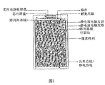
- Figure 1 shows the existing LCD driver architecture.
- Various types of traces and circuits are arranged around the pixel array, including flexible circuit board pads (FPC pads), chip pads (IC pads), and arrays outside the array ( WOA), Fanout, Demultiplexer (DE-MUX), ESD SR (Electrostatic Discharge SR (Trigger)), Array Substrate Row Drive (GOA), and Common Bus/Electrostatic Discharge (Com Bus/ESD)
- the present invention relates to the DE-MUX shown in FIG.
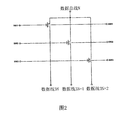
- FIG. 2 shows the DEMUX circuit used in existing LCDs.
- the DEMUX circuit comprises three thin film transistors, wherein the gates of the three thin film transistors respectively input signals SW1, SW2 and SW3, the source/drain are respectively connected to the Data Bus N, and the drain/source are respectively connected to the Data Line. (data lines) 3N, 3N+1 and 3N+2; signals SW1, SW2 and SW3 control the opening and closing of each thin film transistor according to a preset timing, and when the thin film transistor is turned on, the Data Bus N can communicate with the corresponding Data Line and Charge it.
- the DEMUX circuit is usually used in conjunction with the LTPS process. Since the electron mobility of the LTPS process is relatively high, the DE-MUX circuit can still maintain a relatively high data line charging rate.
- IGZO processes and Amorphous Silicon processes also require the use of DEMUX.
- DEMUX the electron mobility is much lower than that of the LTPS.
- the panel's charging rate is affected.
- the present invention provides a DEMUX circuit comprising:
- a data bus first, second, and third data lines respectively connected to the first, second, and third units between the data bus and the corresponding first, second, and third data lines;
- Each of the cells includes a first thin film transistor, a second thin film transistor, a third thin film transistor, and a capacitor, and inputs respective first, second, and third switching signals; a gate of the first thin film transistor inputs a first switching signal, The source and the drain respectively input the first switching signal and the gate connected to the second thin film transistor; the source and the drain of the second thin film transistor are respectively connected to the data bus and the corresponding data line; one end of the capacitor is connected to the second thin film transistor a gate, the other end of which inputs a second switching signal; a gate of the third thin film transistor inputs a third switching signal, and a source and a drain thereof are respectively connected to a gate of the second thin film transistor and a constant voltage low potential;
- the first switch signal when the first switch signal is turned on, the first thin film transistor and the second thin film transistor are turned on, and the corresponding data line is precharged; then when the first switch signal is turned off and the second switch signal is turned on, corresponding The data line is charged to a preset potential.
- each unit selects three suitable switch signals as the first, second and third switch signals corresponding to the unit.
- the four switch signals are rectangular waves with a duty ratio of 0.25, and the phases are different by one quarter cycle.
- the second unit synchronously precharges the second data line, when the second When the unit charges the second data line to the preset potential, the third unit synchronously precharges the third data line, and when the third unit charges the third data line to the preset potential, the first unit synchronizes to the first data.
- the line is pre-charged.
- the data bus is one cycle every four time periods, and after continuously outputting the RGB data signals, a time period is vacant.
- the invention also provides a DEMUX circuit comprising:
- a data bus first, second, and third data lines respectively connected to the first, second, and third units between the data bus and the corresponding first, second, and third data lines;
- Each of the cells includes a first thin film transistor, a second thin film transistor, a third thin film transistor, and a capacitor, and inputs respective first, second, and third switching signals; a gate of the first thin film transistor inputs a first switching signal, The source and the drain respectively input the first switching signal and the gate connected to the second thin film transistor; the source and the drain of the second thin film transistor are respectively connected to the data bus and the corresponding data line; one end of the capacitor is connected to the second thin film transistor a gate, the other end of which inputs a second switching signal; a gate of the third thin film transistor inputs a third switching signal, and a source and a drain thereof are respectively connected to a gate of the second thin film transistor and a constant voltage low potential;
- the first switch signal when the first switch signal is turned on, the first thin film transistor and the second thin film transistor are turned on, and the corresponding data line is precharged; then when the first switch signal is turned off and the second switch signal is turned on, corresponding The data line is charged to a preset potential;
- each unit selects three suitable switch signals as the first, second and third switch signals corresponding to the unit;
- the DEMUX circuit of the present invention can increase the gate driving voltage of the TFT, thereby improving the electron mobility of the IGZO and Amorphous silicon process TFTs and increasing the data line charging rate.
- FIG. 1 is a schematic diagram of a conventional LCD driving architecture
- FIG. 2 is a schematic diagram of a DEMUX circuit used in an existing LCD
- FIG. 3 is a schematic diagram of a DEMUX circuit of the present invention.
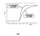
- FIG. 5 is a schematic diagram showing the comparison of the charging waveforms of the DEMUX circuit and the existing DEMUX circuit of the present invention.
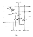
- FIG. 3 is a schematic illustration of the DEMUX circuit of the present invention.
- the DEMUX circuit includes data a data bus N, first, second and third data lines (Data Line) 3N, 3N+1 and 3N+2, respectively connected to the first and second between the data bus N and the corresponding data line And the third unit.
- the first unit includes a first thin film transistor TFT A1, a second thin film transistor TFT A2, a third thin film transistor TFT A3, and a capacitor CAP1;
- the second unit includes a TFT B1, a TFT B2, a TFT B3, and a capacitor CAP2;
- the third unit includes TFT C1, TFT C2, TFT C3, and capacitor CAP3.
- the gate of the first thin film transistor TFT A1 is input to the first switching signal SW1, and the source and the drain thereof are respectively input to the first switching signal SW1 and the gate of the second thin film transistor TFT A2;
- the source and the drain of the second thin film transistor TFT A2 are respectively connected to the data bus N and the corresponding first data line 3N;
- One end of the capacitor CAP1 is connected to the gate of the second thin film transistor TFT A2, and the other end is input to the second switch signal SW2;
- the gate of the third thin film transistor TFT A3 is input to the third switching signal SW3, and the source and the drain thereof are respectively connected to the gate of the second thin film transistor TFT A2 and the constant voltage low potential VGL;
- the first switching signal SW1 when operating, when the first switching signal SW1 is turned on, the first thin film transistor TFT A1 and the second thin film transistor TFT A2 are turned on, the corresponding first data line 3N is precharged; then when the first switching signal SW1 is turned off When the second switch signal SW2 is turned on, the corresponding first data line 3N is charged to a preset potential.
- the first switch signal when the first switch signal is turned on, the first thin film transistor and the second thin film transistor are turned on, and the corresponding data line is precharged; then when the first switch signal is turned off and the second switch signal is turned on, corresponding The data line is charged to a preset potential.
- the respective switching signals of the other units are distinguished from the respective switching signals of the first unit.
- a constant voltage low potential VGL can be used for discharge recovery of each capacitor.
- the capacitor CAP1 can be discharged by the constant voltage low potential VGL.
- the present invention can simultaneously control the operations of the first, second, and third units by providing the switching signals SW1, SW2, SW3, and SW4 and setting appropriate timings; each unit selects three suitable switching signals therein as corresponding The first, second and third switching signals of the unit.
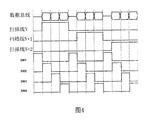
- the four switching signals can be rectangular waves with a duty cycle of 0.25, which are one-fourth of a phase apart from each other (see Figure 4).
- FIGS. 3 and 4 are a timing diagram of the DEMUX circuit of the present invention.
- the operation of the DEMUX circuit of the present invention can be understood in conjunction with FIGS. 3 and 4.
- SW1 is turned on, TFT A1 and TFT A2 are hit.
- Data line3N is pre-charged; then SW1 is turned off, SW2 is turned on, and the gate potential of TFT A2 is further increased by the coupling of capacitor CAP1, Data line3N is charged to a preset potential, and Data line3N+1 is pre-charged;
- SW2 is turned off, SW3 is turned on, and the gate potential of TFT B2 is further increased by the coupling action of the capacitor CAP2,
- Data line3N+1 is charged to a preset potential, and the data line 3N+2 is precharged, and the TFT A3 is turned on, and the TFT A2 is turned on. Close; loop this way.
- the DEMUX circuit of the present invention can be connected to an RGB three primary color display panel to output RGB data signals.
- the data bus Data Bus is one cycle every 4 time periods, and after RGB data signals are continuously output, it is vacant for a period of time.
- the corresponding display panel's Gate line is one cycle every four time periods, three of which are in the on state and one is in the off state.
- the switching signals SW1 to SW4 are one cycle every four time periods, wherein only one time period is in an on state, and the remaining time periods are in a closed state.
- Figure 5 is a comparison of the charging waveforms of the DEMUX circuit of the present invention and the existing DEMUX circuit.
- the horizontal axis is time (in seconds) and the vertical axis is voltage (in volts).
- the Data line charging rate has been greatly improved.
- the DEMUX circuit of the present invention can increase the gate driving voltage of the TFT, thereby improving the electron mobility of the IGZO and Amorphous silicon process TFTs and increasing the data line charging rate.
Landscapes
- Engineering & Computer Science (AREA)
- Chemical & Material Sciences (AREA)
- Crystallography & Structural Chemistry (AREA)
- Physics & Mathematics (AREA)
- Computer Hardware Design (AREA)
- General Physics & Mathematics (AREA)
- Theoretical Computer Science (AREA)
- Liquid Crystal Display Device Control (AREA)
- Control Of Indicators Other Than Cathode Ray Tubes (AREA)
- Liquid Crystal (AREA)
Abstract
一种DEMUX电路,该DEMUX电路包括:数据总线,第一、第二及第三数据线,分别连接于数据总线和相应的第一、第二及第三数据线之间的第一、第二及第三单元;每个单元分别包括第一薄膜晶体管,第二薄膜晶体管,第三薄膜晶体管以及电容,并且输入相应的第一、第二及第三开关信号;对于每个单元,工作时,当第一开关信号打开时,第一薄膜晶体管和第二薄膜晶体管打开,对应的数据线预充电;然后当第一开关信号关闭,第二开关信号打开时,对应的数据线充电至预设电位。该DEMUX电路可以提高TFT栅极驱动电压,进而提高IGZO和Amorphous Silicon制程TFT的电子迁移率,提升数据线充电率。
Description
本发明涉及液晶显示技术领域,尤其涉及一种DEMUX电路。
液晶显示器是目前使用最广泛的一种平板显示器,已经逐渐成为各种电子设备如移动电话、个人数字助理(PDA)、数字相机、计算机屏幕或笔记本电脑屏幕所广泛应用具有高分辨率彩色屏幕的显示器。随着液晶显示器技术的发展进步,人们对液晶显示器的显示品质,外观设计等提出了更高的要求,低成本和窄边框成为人们追求的目标。
解复用器(demultiplexer,简写DEMUX),用于把一个信号通道分解为多个信号通道,在中小尺寸液晶显示器中被广泛采用。在液晶显示器中,DEMUX通常搭配LTPS(低温多晶硅)制程,LTPS制程制作的TFT(薄膜晶体管)器件电子迁移率高,可以满足DEMUX需求。
随着液晶显示器向低成本方向发展,IGZO(氧化铟镓锌)制程和Amorphous Silicon(非晶硅)制程也有使用DEMUX的需求,但是由于IGZO制程和Amorphous Silicon制程制作的器件,电子迁移率比LTPS低很多,使用DEMUX后影响面板的充电率。
图1所示为现有LCD驱动架构,像素阵列(Pixel array)周围布置了各类走线及电路,包括柔性电路板焊盘(FPC Pad),芯片焊盘(IC Pad),阵列外布线(WOA),扇出(Fanout),解复用器(DE-MUX),ESD SR(静电放电SR(触发器)),阵列基板行驱动(GOA),以及公共总线/静电放电(Com Bus/ESD),本发明内容涉及图中1所示的DE-MUX。
图2所示为已有LCD中使用的DEMUX电路。该DEMUX电路包括三个薄膜晶体管,该三个薄膜晶体管的栅极分别输入信号SW1,SW2及SW3,源极/漏极分别连接Data Bus(数据总线)N,漏极/源极分别连接Data Line(数据线)3N,3N+1以及3N+2;信号SW1,SW2及SW3按照预设时序控制各个薄膜晶体管的打开与关闭,当薄膜晶体管打开时,Data Bus N可与相应的Data Line连通并向其充电。该种DEMUX电路通常搭配LTPS制程,由于LTPS制程的电子迁移率比较高,使用该种DE-MUX电路仍然可以维持比较高的数据线(Data line)充电率。随着液晶显示器向低成本方向发展,IGZO制程和Amorphous Silicon制程也有使用DEMUX的需求,
但是由于IGZO制程和Amorphous Silicon制程制作的器件,电子迁移率比LTPS低很多,使用DEMUX后影响面板的充电率。
发明内容
因此,本发明的目的在于提供一种DEMUX电路,提升IGZO和Amorphous Silicon制程DEMUX的充电率。
为实现上述目的,本发明提供了一种DEMUX电路,包括:
数据总线,第一、第二及第三数据线,分别连接于数据总线和相应的第一、第二及第三数据线之间的第一、第二及第三单元;
每个单元分别包括第一薄膜晶体管,第二薄膜晶体管,第三薄膜晶体管以及电容,并且输入相应的第一、第二及第三开关信号;第一薄膜晶体管的栅极输入第一开关信号,其源极和漏极分别输入第一开关信号和连接第二薄膜晶体管的栅极;第二薄膜晶体管的源极和漏极分别连接数据总线和对应的数据线;电容的一端连接第二薄膜晶体管的栅极,另一端输入第二开关信号;第三薄膜晶体管的栅极输入第三开关信号,其源极和漏极分别连接第二薄膜晶体管的栅极和恒压低电位;
对于每个单元,工作时,当第一开关信号打开时,第一薄膜晶体管和第二薄膜晶体管打开,对应的数据线预充电;然后当第一开关信号关闭,第二开关信号打开时,对应的数据线充电至预设电位。
其中,用于输入该第一、第二及第三单元的开关信号共有四个,每个单元选择其中适合的三个开关信号作为对应该单元的第一、第二及第三开关信号。
其中,该四个开关信号为占空比为0.25的直方波,相互之间相位相差四分之一周期。
其中,工作时,通过控制每个单元对应的开关信号的时序,使得当第一单元对第一数据线充电至预设电位时,第二单元同步对第二数据线做预充电,当第二单元对第二数据线充电至预设电位时,第三单元同步对第三数据线做预充电,当第三单元对第三数据线充电至预设电位时,第一单元同步对第一数据线做预充电。
其中,其为氧化铟镓锌制程中的DEMUX电路。
其中,其为非晶硅制程中的DEMUX电路。
其中,其连接RGB三基色显示面板以输出RGB数据信号。
其中,该数据总线每4个时间段为一个循环,连续输出RGB数据信号后,空置一个时间段。
本发明还提供一种DEMUX电路,包括:
数据总线,第一、第二及第三数据线,分别连接于数据总线和相应的第一、第二及第三数据线之间的第一、第二及第三单元;
每个单元分别包括第一薄膜晶体管,第二薄膜晶体管,第三薄膜晶体管以及电容,并且输入相应的第一、第二及第三开关信号;第一薄膜晶体管的栅极输入第一开关信号,其源极和漏极分别输入第一开关信号和连接第二薄膜晶体管的栅极;第二薄膜晶体管的源极和漏极分别连接数据总线和对应的数据线;电容的一端连接第二薄膜晶体管的栅极,另一端输入第二开关信号;第三薄膜晶体管的栅极输入第三开关信号,其源极和漏极分别连接第二薄膜晶体管的栅极和恒压低电位;
对于每个单元,工作时,当第一开关信号打开时,第一薄膜晶体管和第二薄膜晶体管打开,对应的数据线预充电;然后当第一开关信号关闭,第二开关信号打开时,对应的数据线充电至预设电位;
其中,用于输入该第一、第二及第三单元的开关信号共有四个,每个单元选择其中适合的三个开关信号作为对应该单元的第一、第二及第三开关信号;
其中,其连接RGB三基色显示面板以输出RGB数据信号。
综上所述,本发明的DEMUX电路可以提高TFT栅极驱动电压,进而提高IGZO和Amorphous Silicon制程TFT的电子迁移率,提升数据线充电率。
下面结合附图,通过对本发明的具体实施方式详细描述,将使本发明的技术方案及其他有益效果显而易见。
附图中,
图1为现有LCD驱动架构示意图;
图2为已有LCD中使用的DEMUX电路示意图;
图3为本发明DEMUX电路的示意图;
图4为本发明DEMUX电路的时序图;
图5为本发明DEMUX电路和已有DEMUX电路充电波形的比较示意图。
图3所示为本发明DEMUX电路的示意图。该DEMUX电路包括数据
总线(Data Bus)N,第一、第二及第三数据线(Data Line)3N,3N+1及3N+2,分别连接于数据总线N和对应的数据线之间的第一、第二及第三单元。
第一单元包括第一薄膜晶体管TFT A1,第二薄膜晶体管TFT A2,第三薄膜晶体管TFT A3,以及电容CAP1;第二单元包括TFT B1,TFT B2,TFT B3,以及电容CAP2;第三单元包括TFT C1,TFT C2,TFT C3,以及电容CAP3。
现以第一单元为例对各单元结构和功能加以详细说明,第一单元中:
第一薄膜晶体管TFT A1的栅极输入第一开关信号SW1,其源极和漏极分别输入第一开关信号SW1和连接第二薄膜晶体管TFT A2的栅极;
第二薄膜晶体管TFT A2的源极和漏极分别连接数据总线N和对应的第一数据线3N;
电容CAP1的一端连接第二薄膜晶体管TFT A2的栅极,另一端输入第二开关信号SW2;
第三薄膜晶体管TFT A3的栅极输入第三开关信号SW3,其源极和漏极分别连接第二薄膜晶体管TFT A2的栅极和恒压低电位VGL;
对于第一单元,工作时,当第一开关信号SW1打开时,第一薄膜晶体管TFT A1和第二薄膜晶体管TFT A2打开,对应的第一数据线3N预充电;然后当第一开关信号SW1关闭,第二开关信号SW2打开时,对应的第一数据线3N充电至预设电位。
对于其他单元,工作时,当第一开关信号打开时,第一薄膜晶体管和第二薄膜晶体管打开,对应的数据线预充电;然后当第一开关信号关闭,第二开关信号打开时,对应的数据线充电至预设电位。其他单元的各开关信号区别于第一单元的各开关信号。
此外,恒压低电位VGL可用于各电容的放电回复。例如对于第一单元,当开关信号SW2关闭,开关信号SW3打开时,电容CAP1可通过恒压低电位VGL放电回复。
进一步,本发明可以通过提供开关信号SW1,SW2,SW3及SW4并设置适合的时序来同时控制第一、第二及第三单元的工作;每个单元选择其中适合的三个开关信号作为对应该单元的第一、第二及第三开关信号。该四个开关信号可以为占空比为0.25的直方波,相互之间相位相差四分之一周期(可参见图4)。
图4所示为本发明DEMUX电路的时序图。结合图3及图4可以理解本发明DEMUX电路的工作原理。当SW1打开时,TFT A1和TFT A2被打
开,Data line3N做预充电;然后SW1关闭,SW2打开,通过电容CAP1的耦合作用,使TFT A2的栅极电位进一步提升,Data line3N充电至预设电位,同步Data line3N+1做预充电;然后SW2关闭,SW3打开,通过电容CAP2的耦合作用,使TFT B2的栅极电位进一步提升,Data line3N+1充电至预设电位,同步Data line3N+2做预充电,此时TFT A3打开,TFT A2关闭;以此循环。
参见DEMUX电路的时序图,可以将本发明的DEMUX电路连接RGB三基色显示面板以输出RGB数据信号。数据总线Data Bus每4个时间段为一个循环,连续输出RGB数据信号后,空置一个时间段。此时相应的显示面板的扫描线(Gate line)每4个时间段为一个循环,其中三个处于开启状态,一个处于关闭状态。开关信号SW1~SW4,每4个时间段为一个循环,其中只有一个时间段处于开启状态,其余时间段处于关闭状态。
图5所示为本发明DEMUX电路和已有DEMUX电路充电波形的比较,横轴为时间(单位秒),纵轴为电压(单位伏特),由图可以看出,使用本发明DEMUX电路后,Data line充电率得到大幅提升。
综上所述,本发明的DEMUX电路可以提高TFT栅极驱动电压,进而提高IGZO和Amorphous Silicon制程TFT的电子迁移率,提升数据线充电率。
以上所述,对于本领域的普通技术人员来说,可以根据本发明的技术方案和技术构思作出其他各种相应的改变和变形,而所有这些改变和变形都应属于本发明后附的权利要求的保护范围。
Claims (14)
- 一种DEMUX电路,包括:数据总线,第一、第二及第三数据线,分别连接于数据总线和相应的第一、第二及第三数据线之间的第一、第二及第三单元;每个单元分别包括第一薄膜晶体管,第二薄膜晶体管,第三薄膜晶体管以及电容,并且输入相应的第一、第二及第三开关信号;第一薄膜晶体管的栅极输入第一开关信号,其源极和漏极分别输入第一开关信号和连接第二薄膜晶体管的栅极;第二薄膜晶体管的源极和漏极分别连接数据总线和对应的数据线;电容的一端连接第二薄膜晶体管的栅极,另一端输入第二开关信号;第三薄膜晶体管的栅极输入第三开关信号,其源极和漏极分别连接第二薄膜晶体管的栅极和恒压低电位;对于每个单元,工作时,当第一开关信号打开时,第一薄膜晶体管和第二薄膜晶体管打开,对应的数据线预充电;然后当第一开关信号关闭,第二开关信号打开时,对应的数据线充电至预设电位。
- 如权利要求1所述的DEMUX电路,其中,用于输入该第一、第二及第三单元的开关信号共有四个,每个单元选择其中适合的三个开关信号作为对应该单元的第一、第二及第三开关信号。
- 如权利要求2所述的DEMUX电路,其中,该四个开关信号为占空比为0.25的直方波,相互之间相位相差四分之一周期。
- 如权利要求3所述的DEMUX电路,其中,工作时,通过控制每个单元对应的开关信号的时序,使得当第一单元对第一数据线充电至预设电位时,第二单元同步对第二数据线做预充电,当第二单元对第二数据线充电至预设电位时,第三单元同步对第三数据线做预充电,当第三单元对第三数据线充电至预设电位时,第一单元同步对第一数据线做预充电。
- 如权利要求1所述的DEMUX电路,其中,其为氧化铟镓锌制程中的DEMUX电路。
- 如权利要求1所述的DEMUX电路,其中,其为非晶硅制程中的DEMUX电路。
- 如权利要求1所述的DEMUX电路,其中,其连接RGB三基色显示面板以输出RGB数据信号。
- 如权利要求7所述的DEMUX电路,其中,该数据总线每4个时间段为一个循环,连续输出RGB数据信号后,空置一个时间段。
- 一种DEMUX电路,包括:数据总线,第一、第二及第三数据线,分别连接于数据总线和相应的第一、第二及第三数据线之间的第一、第二及第三单元;每个单元分别包括第一薄膜晶体管,第二薄膜晶体管,第三薄膜晶体管以及电容,并且输入相应的第一、第二及第三开关信号;第一薄膜晶体管的栅极输入第一开关信号,其源极和漏极分别输入第一开关信号和连接第二薄膜晶体管的栅极;第二薄膜晶体管的源极和漏极分别连接数据总线和对应的数据线;电容的一端连接第二薄膜晶体管的栅极,另一端输入第二开关信号;第三薄膜晶体管的栅极输入第三开关信号,其源极和漏极分别连接第二薄膜晶体管的栅极和恒压低电位;对于每个单元,工作时,当第一开关信号打开时,第一薄膜晶体管和第二薄膜晶体管打开,对应的数据线预充电;然后当第一开关信号关闭,第二开关信号打开时,对应的数据线充电至预设电位;其中,用于输入该第一、第二及第三单元的开关信号共有四个,每个单元选择其中适合的三个开关信号作为对应该单元的第一、第二及第三开关信号;其中,其连接RGB三基色显示面板以输出RGB数据信号。
- 如权利要求9所述的DEMUX电路,其中,该四个开关信号为占空比为0.25的直方波,相互之间相位相差四分之一周期。
- 如权利要求10所述的DEMUX电路,其中,工作时,通过控制每个单元对应的开关信号的时序,使得当第一单元对第一数据线充电至预设电位时,第二单元同步对第二数据线做预充电,当第二单元对第二数据线充电至预设电位时,第三单元同步对第三数据线做预充电,当第三单元对第三数据线充电至预设电位时,第一单元同步对第一数据线做预充电。
- 如权利要求9所述的DEMUX电路,其中,其为氧化铟镓锌制程中的DEMUX电路。
- 如权利要求9所述的DEMUX电路,其中,其为非晶硅制程中的DEMUX电路。
- 如权利要求9所述的DEMUX电路,其中,该数据总线每4个时间段为一个循环,连续输出RGB数据信号后,空置一个时间段。
Priority Applications (1)
| Application Number | Priority Date | Filing Date | Title |
|---|---|---|---|
| US15/540,028 US10431179B2 (en) | 2017-04-17 | 2017-05-18 | DEMUX circuit |
Applications Claiming Priority (2)
| Application Number | Priority Date | Filing Date | Title |
|---|---|---|---|
| CN201710250566.3 | 2017-04-17 | ||
| CN201710250566.3A CN107016970B (zh) | 2017-04-17 | 2017-04-17 | Demux电路 |
Publications (1)
| Publication Number | Publication Date |
|---|---|
| WO2018192049A1 true WO2018192049A1 (zh) | 2018-10-25 |
Family
ID=59447873
Family Applications (1)
| Application Number | Title | Priority Date | Filing Date |
|---|---|---|---|
| PCT/CN2017/084955 Ceased WO2018192049A1 (zh) | 2017-04-17 | 2017-05-18 | Demux电路 |
Country Status (2)
| Country | Link |
|---|---|
| CN (1) | CN107016970B (zh) |
| WO (1) | WO2018192049A1 (zh) |
Families Citing this family (10)
| Publication number | Priority date | Publication date | Assignee | Title |
|---|---|---|---|---|
| CN107016970B (zh) * | 2017-04-17 | 2019-12-24 | 深圳市华星光电半导体显示技术有限公司 | Demux电路 |
| US10431179B2 (en) | 2017-04-17 | 2019-10-01 | Shenzhen China Star Optoelectronics Semiconductor Display Technology Co., Ltd. | DEMUX circuit |
| KR102668922B1 (ko) * | 2018-07-20 | 2024-05-23 | 엘지디스플레이 주식회사 | 표시 장치 |
| KR102594624B1 (ko) * | 2018-07-20 | 2023-10-25 | 엘지디스플레이 주식회사 | 표시 장치 |
| CN109087590B (zh) * | 2018-10-24 | 2020-10-02 | 武汉天马微电子有限公司 | 一种显示面板及显示装置 |
| KR102748472B1 (ko) | 2018-12-05 | 2024-12-30 | 엘지디스플레이 주식회사 | 표시 장치 |
| CN110910845A (zh) * | 2019-11-18 | 2020-03-24 | 福建华佳彩有限公司 | Dot显示的驱动方法 |
| KR102730294B1 (ko) * | 2019-12-31 | 2024-11-13 | 엘지디스플레이 주식회사 | 표시 장치 |
| KR102705900B1 (ko) * | 2019-12-31 | 2024-09-10 | 엘지디스플레이 주식회사 | 표시 장치 |
| CN112837648A (zh) * | 2021-02-25 | 2021-05-25 | 福建华佳彩有限公司 | 一种Demux显示屏驱动电路及其控制方法 |
Citations (4)
| Publication number | Priority date | Publication date | Assignee | Title |
|---|---|---|---|---|
| US20050243043A1 (en) * | 2004-04-30 | 2005-11-03 | Lg.Philips Lcd Co., Ltd. | Liquid crystal display and pre-charging method thereof |
| CN1952765A (zh) * | 2006-11-07 | 2007-04-25 | 友达光电股份有限公司 | 解复用器的布局结构及具有该解复用器的液晶显示面板 |
| CN106469547A (zh) * | 2015-08-21 | 2017-03-01 | 三星显示有限公司 | 解复用器、显示设备以及用于驱动该显示设备的方法 |
| CN107016970A (zh) * | 2017-04-17 | 2017-08-04 | 深圳市华星光电技术有限公司 | Demux电路 |
Family Cites Families (5)
| Publication number | Priority date | Publication date | Assignee | Title |
|---|---|---|---|---|
| JP4927216B1 (ja) * | 2010-11-12 | 2012-05-09 | シャープ株式会社 | 線形素子列値推定方法、静電容量検出方法、集積回路、タッチセンサシステム、及び電子機器 |
| US8674918B1 (en) * | 2011-09-05 | 2014-03-18 | Nongqiang Fan | Method of driving active matrix displays |
| KR102318144B1 (ko) * | 2015-05-08 | 2021-10-28 | 삼성디스플레이 주식회사 | 표시 장치 및 그것의 구동 방법 |
| CN105335013A (zh) * | 2015-12-03 | 2016-02-17 | 深圳磨石科技有限公司 | 触摸显示装置和电子设备 |
| CN106128354B (zh) * | 2016-09-12 | 2018-01-30 | 武汉华星光电技术有限公司 | 平面显示装置及其扫描驱动电路 |
-
2017
- 2017-04-17 CN CN201710250566.3A patent/CN107016970B/zh active Active
- 2017-05-18 WO PCT/CN2017/084955 patent/WO2018192049A1/zh not_active Ceased
Patent Citations (4)
| Publication number | Priority date | Publication date | Assignee | Title |
|---|---|---|---|---|
| US20050243043A1 (en) * | 2004-04-30 | 2005-11-03 | Lg.Philips Lcd Co., Ltd. | Liquid crystal display and pre-charging method thereof |
| CN1952765A (zh) * | 2006-11-07 | 2007-04-25 | 友达光电股份有限公司 | 解复用器的布局结构及具有该解复用器的液晶显示面板 |
| CN106469547A (zh) * | 2015-08-21 | 2017-03-01 | 三星显示有限公司 | 解复用器、显示设备以及用于驱动该显示设备的方法 |
| CN107016970A (zh) * | 2017-04-17 | 2017-08-04 | 深圳市华星光电技术有限公司 | Demux电路 |
Also Published As
| Publication number | Publication date |
|---|---|
| CN107016970A (zh) | 2017-08-04 |
| CN107016970B (zh) | 2019-12-24 |
Similar Documents
| Publication | Publication Date | Title |
|---|---|---|
| WO2018192049A1 (zh) | Demux电路 | |
| US10431179B2 (en) | DEMUX circuit | |
| US9659540B1 (en) | GOA circuit of reducing power consumption | |
| US10825414B2 (en) | Scanning signal line drive circuit, display device provided with same, and drive method for scanning signal line | |
| US9405392B2 (en) | Display device having partial panels and driving method thereof | |
| CN100510855C (zh) | 液晶显示器及其预充电方法 | |
| US9818362B2 (en) | Charging scan and charge sharing scan double output GOA circuit | |
| US8698852B2 (en) | Display device and method for driving the same | |
| US10770018B2 (en) | Scanning signal line drive circuit, display device including the same, and scanning signal line driving method | |
| WO2019041853A1 (zh) | 移位寄存器单元、驱动装置、显示装置以及驱动方法 | |
| US20060269038A1 (en) | Shift register | |
| CN108628049B (zh) | 阵列基板、显示面板及显示装置 | |
| US11482184B2 (en) | Row drive circuit of array substrate and display device | |
| JP2017037298A (ja) | 表示装置 | |
| JP2015232602A (ja) | 表示装置 | |
| TW200405235A (en) | Shift register and liquid crystal display having the same | |
| US10459263B2 (en) | Display panel and borderless type display including the same | |
| CN108242227A (zh) | 显示装置以及单位寄存器电路 | |
| US11107388B2 (en) | Gate driving circuit and display device using the same | |
| CN107909979A (zh) | 液晶显示装置及改善显示面板掉电闪屏的方法 | |
| US11462187B2 (en) | Row drive circuit of array substrate and display device | |
| US10386663B2 (en) | GOA circuit and liquid crystal display device | |
| JP6383575B2 (ja) | 表示装置 | |
| CN112992094A (zh) | 一种gip电路驱动方法及显示装置 | |
| KR20110109473A (ko) | 액정 표시장치의 구동장치 |
Legal Events
| Date | Code | Title | Description |
|---|---|---|---|
| WWE | Wipo information: entry into national phase |
Ref document number: 15540028 Country of ref document: US |
|
| 121 | Ep: the epo has been informed by wipo that ep was designated in this application |
Ref document number: 17906281 Country of ref document: EP Kind code of ref document: A1 |
|
| NENP | Non-entry into the national phase |
Ref country code: DE |
|
| 122 | Ep: pct application non-entry in european phase |
Ref document number: 17906281 Country of ref document: EP Kind code of ref document: A1 |