WO2018185997A1 - 半導体パッケージ及び半導体デバイス - Google Patents
半導体パッケージ及び半導体デバイス Download PDFInfo
- Publication number
- WO2018185997A1 WO2018185997A1 PCT/JP2018/001707 JP2018001707W WO2018185997A1 WO 2018185997 A1 WO2018185997 A1 WO 2018185997A1 JP 2018001707 W JP2018001707 W JP 2018001707W WO 2018185997 A1 WO2018185997 A1 WO 2018185997A1
- Authority
- WO
- WIPO (PCT)
- Prior art keywords
- semiconductor element
- side wall
- sealing material
- material layer
- semiconductor
- Prior art date
- Legal status (The legal status is an assumption and is not a legal conclusion. Google has not performed a legal analysis and makes no representation as to the accuracy of the status listed.)
- Ceased
Links
Images
Classifications
-
- H—ELECTRICITY
- H10—SEMICONDUCTOR DEVICES; ELECTRIC SOLID-STATE DEVICES NOT OTHERWISE PROVIDED FOR
- H10W—GENERIC PACKAGES, INTERCONNECTIONS, CONNECTORS OR OTHER CONSTRUCTIONAL DETAILS OF DEVICES COVERED BY CLASS H10
- H10W76/00—Containers; Fillings or auxiliary members therefor; Seals
- H10W76/10—Containers or parts thereof
Definitions
- the present invention relates to a semiconductor package for mounting and sealing a semiconductor element and a semiconductor device using the semiconductor package.
- a package is used for mounting and sealing an element.
- a package includes, for example, a container in which an element can be mounted and a cover member for sealing the inside of the container.
- a solid-state imaging element such as a CCD or a CMOS, a light emitting element, or a MEMS is known.
- Patent Document 1 discloses a package for housing an electronic element.
- the package of patent document 1 is provided with the package board
- the step portion of the package substrate and the lid body are bonded via a bonding layer provided therebetween.
- the bonding layer is preferably composed of a sealing material made of low-melting glass such as bismuth glass.
- such a sealing material is irradiated with a laser through a lid to melt and solidify the sealing material, thereby joining the stepped portion of the package substrate and the lid.
- An object of the present invention is to provide a semiconductor package and a semiconductor device using the semiconductor package, in which a soft error of a semiconductor element due to the ionizing action of ⁇ rays hardly occurs.
- a semiconductor package according to the present invention is a semiconductor package for mounting and sealing a semiconductor element, and includes a bottom portion on which the semiconductor element is mounted and a frame-shaped side wall portion disposed on the bottom portion.
- a sealing material disposed between the container, the side wall of the container, a glass lid for sealing the inside of the container, and the side wall of the container and the glass lid A side wall portion is provided so that a part of the side wall portion exists between an upper end portion of the sealing material layer on the semiconductor element side and an outer peripheral edge of the upper surface of the semiconductor element. It is characterized by having.
- the thickness of the sealing material layer is A, and the distance in plan view between the upper end portion of the sealing material layer on the semiconductor element side and the upper end portion of the side wall portion on the semiconductor element side.
- B is the ratio A / B, and the difference in height between the upper surface of the side wall portion and the upper surface of the semiconductor element is C, and the upper end portion of the side wall portion on the semiconductor element side and the semiconductor element It is preferable that the ratio C / D, where D is the distance in plan view from the upper end on the side opposite to the sealing material layer, satisfies A / B ⁇ C / D.
- the sealing material layer is preferably made of glass frit.
- the glass frit includes bismuth glass.
- a semiconductor device includes a semiconductor package configured according to the present invention, and a semiconductor element housed in the semiconductor package.
- the semiconductor element is preferably a solid-state imaging element.
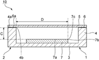
- FIG. 1 is a schematic cross-sectional view showing a semiconductor package and a semiconductor device according to an embodiment of the present invention.
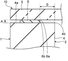
- FIG. 2 is an enlarged schematic cross-sectional view showing a portion where a sealing material layer is provided in a semiconductor package and a semiconductor device according to an embodiment of the present invention.
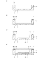
- 3A to 3D are schematic cross-sectional views for explaining a method for manufacturing a semiconductor package according to an embodiment of the present invention.
- FIG. 1 is a schematic cross-sectional view showing a semiconductor package and a semiconductor device according to an embodiment of the present invention.
- FIG. 2 is an enlarged schematic cross-sectional view showing a portion where the sealing material layer is provided in the semiconductor package and the semiconductor device according to the embodiment of the present invention.
- the semiconductor package 1 is a semiconductor package for mounting and sealing a semiconductor element 7.
- Examples of the semiconductor element 7 mounted on the semiconductor package 1 include a solid-state imaging element such as a CCD or a CMOS.
- the semiconductor package 1 includes a container 2, a glass lid 5, and a sealing material layer 6.
- the container 2 is configured by LTCC (Low Temperature Co-fired Ceramics). But the container 2 may be comprised with another material and the material of the container 2 is not specifically limited.
- LTCC Low Temperature Co-fired Ceramics
- the container 2 has a bottom part 3 and a side wall part 4.
- the bottom portion 3 is a portion where the semiconductor element 7 is mounted in the container 2.
- a glass lid 5 is disposed on the upper surface 4 a of the side wall 4.
- the glass lid 5 is a member for sealing the container 2.
- a sealing material layer 6 is provided between the side wall portion 4 and the glass lid 5.
- the side wall 4 and the glass lid 5 are joined together by the sealing material layer 6.
- the sealing material layer 6 is made of glass frit containing bismuth glass. But the sealing material layer 6 may be comprised with another material, and is not specifically limited.
- the cross-sectional shape of the sealing material layer 6 is rectangular, but the side surface 6b of the sealing material layer 6 may have a rounded shape, and the shape of the sealing material layer 6 Is not particularly limited.
- the side wall portion 4 is provided so that a part of the side wall portion 4 exists between the upper end portion 6 a of the sealing material layer 6 and the outer peripheral edge 7 b of the semiconductor element 7. Yes.
- the upper end portion 6a of the sealing material layer 6 is the upper end portion of the sealing material layer 6 on the semiconductor element 7 side.
- the outer peripheral edge 7 b is an outer peripheral edge on the upper surface 7 a of the semiconductor element 7.
- the side wall 4 is provided between the upper end 6 a of the sealing material layer 6 and the upper end 7 c of the semiconductor element 7 so that a part of the side wall 4 exists.
- the upper end portion 7 c of the semiconductor element 7 is the upper end portion of the semiconductor element 7 opposite to the upper end portion 6 a of the sealing material layer 6.
- the side wall 4 is provided between the upper end 6 a of the sealing material layer 6 and the outer peripheral edge 7 b of the semiconductor element 7 so that a part of the side wall 4 exists.
- a soft error of the semiconductor element 7 due to the ionization effect of the wire hardly occurs. This can be explained as follows.
- the side wall portion 4 and the glass lid 5 are joined using the glass frit containing bismuth-based glass as described above.
- the glass frit containing bismuth-based glass may contain impurities that emit ⁇ rays, such as lead. Therefore, in a conventional semiconductor package using such a glass frit, a soft error of the semiconductor element may occur due to the ionizing action of ⁇ rays emitted from the glass frit.
- a part of the side wall portion 4 is present between the upper end portion 6a of the sealing material layer 6 and the outer peripheral edge 7b of the semiconductor element 7 as described above.
- a side wall 4 is provided on the side. Therefore, ⁇ -rays emitted from the sealing material layer 6 toward the semiconductor element 7 can be shielded by the side wall portion 4. Therefore, it is difficult for the ⁇ -rays emitted from the sealing material layer 6 to be applied to the semiconductor element 7, and soft errors of the semiconductor element 7 due to the ionizing action of the ⁇ -rays can be prevented.
- the semiconductor package 1 since a part of the side wall portion 4 exists on all straight lines connecting the upper end portion 6 a of the sealing material layer 6 and the outer peripheral edge 7 b of the semiconductor element 7, sealing is performed.
- the ⁇ rays emitted from the material layer 6 toward the semiconductor element 7 can be shielded by the side wall portion 4, thereby making it difficult to cause a soft error of the semiconductor element 7 due to the ionizing action of the ⁇ rays.
- the sealing material layer 6 when the shape in the cross section of the sealing material layer 6 is not rectangular, for example, when the side surface 6b of the sealing material layer 6 has a rounded shape, the sealing material layer 6
- the side wall portion 4 is preferably provided so that a part of the side wall portion 4 exists between the portion of the side surface 6 b closest to the semiconductor element 7 and the outer peripheral edge 7 b of the semiconductor element 7. In this case, the ⁇ -rays can be more reliably shielded by the side wall portion 4, and the soft error of the semiconductor element 7 due to the ionizing action of the ⁇ -rays can be further prevented.
- A, B, C and D shown in FIGS. 1 and 2 satisfy A / B ⁇ C / D.
- A is the thickness of the sealing material layer 6.
- B is a distance in plan view between the upper end portion 6 a of the sealing material layer 6 and the upper end portion 4 b of the side wall portion 4.
- the upper end 4b of the side wall 4 is the upper end of the side wall 4 on the semiconductor element 7 side.
- B is the shortest distance in plan view between the upper end portion 6 a of the sealing material layer 6 and the upper end portion 4 b of the side wall portion 4.
- C is the difference in height between the upper surface 4a of the side wall portion 4 and the upper surface 7a of the semiconductor element 7 (upper surface 4a of the side wall portion 4 ⁇ upper surface 7a of the semiconductor element 7).
- D is a distance in plan view between the upper end 4b of the side wall 4 and the upper end 7c of the semiconductor element 7.
- the upper end portion 7 c of the semiconductor element 7 is the upper end portion of the semiconductor element 7 on the side opposite to the sealing material layer 6. More specifically, the upper end portion 7c of the semiconductor element 7 is the upper end portion of the semiconductor element 7 provided on the side opposite to the upper end portion 6a of the sealing material layer 6 used when obtaining B.
- the upper end portion 7 c of the semiconductor element 7 is a portion of the outer peripheral edge 7 b of the semiconductor element 7 that is farthest from the upper end portion 6 a of the sealing material layer 6 used when obtaining B.
- a / B (ratio of A to B) is preferably less than 0.1, more preferably 0.05 or less.
- a / B is less than or equal to the above upper limit, the ⁇ -rays can be more reliably shielded by the side wall portion 4, and the soft error of the semiconductor element 7 due to the ionizing action of the ⁇ -rays can be further reduced.
- a / B is preferably 0.001 or more. In this case, the bonding strength between the side wall portion 4 and the glass lid 5 can be further increased.
- C / D (ratio of C to D) is preferably 0.05 or more, more preferably 0.1 or more.
- the upper limit value of C / D can be set to 50, for example.
- the container 2 has a bottom 3 and a side wall 4.
- the container 2 may be one in which the bottom portion 3 and the side wall portion 4 are integrally molded, or may be one in which the bottom portion 3 and the side wall portion 4 are separately molded and joined by an adhesive or the like. Good.
- the container 2 is made of, for example, ceramic or glass ceramic.
- the ceramic include aluminum oxide, aluminum nitride, zirconia, and mullite.
- the glass ceramic include LTCC (Low Temperature Co-fired Ceramics). Specific examples of LTCC include a sintered body of an inorganic powder such as titanium oxide or niobium oxide and a glass powder.
- Glass lid examples of the glass constituting the glass lid 5 include SiO 2 —B 2 O 3 —RO (R is Mg, Ca, Sr or Ba) -based glass, SiO 2 —B 2 O 3 —R ′ 2 O (R ′ Is Li, Na or Ka) glass, SiO 2 —B 2 O 3 —RO—R ′ 2 O glass (R ′ is Li, Na or Ka), SnO—P 2 O 5 glass, TeO 2 glass Alternatively, Bi 2 O 3 glass or the like can be used.
- R is Mg, Ca, Sr or Ba
- glass frit As a sealing material for forming the sealing material layer 6, for example, glass frit can be used. Among them, it contains a glass frit having a low melting point such as Bi 2 O 3 glass powder (bismuth glass powder), SnO—P 2 O 5 glass powder, V 2 O 5 —TeO 2 glass powder. preferable. In particular, when sealing is performed by irradiating with a laser, the glass frit has a bismuth-based material having a very low softening point from the viewpoint of further increasing the bonding strength and the necessity of softening the sealing material by heating in a shorter time. It is more preferable to use glass powder.
- bismuth glass powder bismuth glass powder
- the glass frit may contain a low expansion refractory filler, a laser absorber and the like.
- a low expansion refractory filler include cordierite, willemite, alumina, zirconium phosphate compounds, zircon, zirconia, tin oxide, quartz glass, ⁇ -quartz solid solution, ⁇ -eucryptite, and spodumene.
- the laser absorbing material include compounds such as at least one metal selected from Fe, Mn, Cu and the like or an oxide containing the metal.
- the semiconductor device 10 includes the semiconductor package 1 and the semiconductor element 7 described above.
- the semiconductor element 7 is accommodated in the semiconductor package 1. Since the semiconductor device 10 includes the semiconductor package 1, the soft error of the semiconductor element 7 due to the ionizing action of ⁇ rays hardly occurs.
- a solid-state imaging element such as a CCD or a CMOS can be suitably used as the semiconductor element 7.
- a container 2 having a bottom 3 and a side wall 4 is prepared.
- a sealing material is printed on the upper surface 4 a of the side wall portion 4 of the container 2.
- the sealing material for example, a glass frit containing bismuth glass can be used.
- the sealing material is dried and further subjected to heat treatment to sinter the sealing material to form the sealing material layer 6.
- the sealing material layer 6 may be formed on the glass lid 5 side.
- the semiconductor element 7 is mounted on the bottom 3 of the container 2.
- a part of the side wall part 4 exists between the upper end part 6a of the sealing material layer 6 and the outer peripheral edge 7b of the semiconductor element 7.
- the side wall part 4 and the sealing material layer 6 shall be formed.
- a glass lid 5 is disposed on a portion where the sealing material layer 6 is provided on the upper surface 4 a of the side wall portion 4.
- position the glass cover 5 it is preferable to arrange
- the sealing material layer 6 is softened by irradiating a laser from a laser light source with the glass lid 5 disposed on the upper surface 4a of the side wall portion 4 via the sealing material layer 6, and the container 2 The side wall portion 4 and the glass lid 5 are joined. Thereby, the inside of the container 2 is hermetically sealed to obtain the semiconductor package 1 and the semiconductor device 10 shown in FIG. According to this method, since only the sealing material layer 6 can be locally heated, the semiconductor package 1 can be hermetically sealed without degrading the semiconductor element 7 having low heat resistance.
- the laser for example, a laser having a wavelength of 600 nm to 1600 nm can be used.
- a laser from a laser light source is irradiated to the sealing material layer 6 through the glass lid 5.
- the laser scans the upper surface 4a of the frame-like side wall portion 4 and rotates.
- the circulated laser irradiates to a position beyond the starting point of laser irradiation.
- the end point of the laser may be a position beyond the starting point after the laser is circulated, or may be the same position as the starting point.
- the sealing material layer 6 may be softened by simply heating the sealing material layer 6 without irradiating the laser, and the side wall 4 and the glass lid 5 of the container 2 may be joined. Good.
- the side wall 4 is provided between the upper end 6 a of the sealing material layer 6 and the outer peripheral edge 7 b of the semiconductor element 7 so that a part of the side wall 4 exists.
- the soft error of the semiconductor element 7 due to the ionizing action of ⁇ rays hardly occurs.
- Example 1 First, the container which has a bottom part and a side wall part and was comprised by LTCC was prepared.
- a glass frit was printed on the upper surface of the side wall of the container. After printing, the glass frit was sintered by drying and heat treatment to form a sealing material layer.
- the glass frit in mol%, Bi 2 O 3 39% , B 2 O 3 23.7%, 14.1% ZnO, Al 2 O 3 2.7%, CuO 20%, Fe 2 O 3 Glass powder having a composition of 0.5% was used.
- a scintillation counter was set in a predetermined area on the inner bottom of the prepared container, specifically, in an area where the upper surface of the semiconductor element was placed when the semiconductor element was mounted.
- a glass lid was placed on the portion provided with the sealing material layer above the side wall of the container. Subsequently, a portion of the container where the sealing material layer is provided is irradiated with a laser from a laser light source above the glass lid to soften the sealing material layer and bond the side wall of the container and the glass lid. It was. Thereby, the inside of the container was sealed to obtain a semiconductor package.
- the thickness A of the sealing material layer is 5 ⁇ m, and when the semiconductor element is mounted, the upper end portion on the semiconductor element side of the sealing material layer and the upper end portion on the semiconductor element side of the side wall portion are The semiconductor package was designed so that the distance B in plan view was 300 ⁇ m. Further, the height difference C between the upper surface of the side wall portion and the upper surface of the semiconductor element is 400 ⁇ m, and the upper surface of the side wall portion on the semiconductor element side and the upper end portion on the side opposite to the sealing material layer of the semiconductor element are viewed in plan The semiconductor package was designed such that the distance D at 7200 ⁇ m.
- the side wall portion exists between the upper end portion of the sealing material layer on the semiconductor element side and the outer peripheral edge on the upper surface of the semiconductor element.
- Comparative Example 1 In Comparative Example 1, the thickness A of the sealing material layer is 5 ⁇ m, and when the semiconductor element is mounted, the plane between the upper end portion on the semiconductor element side of the sealing material layer and the upper end portion on the semiconductor element side of the side wall portion The semiconductor package was designed so that the visual distance B was 10 ⁇ m. Further, the height difference C between the upper surface of the side wall portion and the upper surface of the semiconductor element is 400 ⁇ m, and the upper surface of the side wall portion on the semiconductor element side and the upper end portion on the side opposite to the sealing material layer of the semiconductor element are viewed in plan A semiconductor package was obtained in the same manner as in Example 1 except that the semiconductor package was designed so that the distance D at 7200 ⁇ m was 7200 ⁇ m.
- ⁇ dose shown below was calculated by dividing the count number measured for 24 hours by the above method (scintillation counter) by the time and the area of the semiconductor element mounting surface.
- Example 1 the ⁇ dose incident on the scintillation counter was 0.00 cph / cm 2 .
- the ⁇ dose incident on the scintillation counter was 2.80 cph / cm 2 .
Landscapes
- Solid State Image Pick-Up Elements (AREA)
Abstract
α線の電離作用による半導体素子のソフトエラーが生じ難い、半導体パッケージを提供する。 半導体素子7を搭載して封止するための半導体パッケージ1であって、半導体素子7が搭載される底部3と該底部3上に配置された枠状の側壁部4とを有する、容器2と、容器2の側壁部4の上方に配置されており、容器2内を封止するためのガラス蓋5と、容器2の側壁部4とガラス蓋5との間に配置されている、封着材料層6と、を備え、封着材料層6の半導体素子7側の上端部6aと半導体素子7の上面7aにおける外周縁7bとの間に、側壁部4の一部が存在するように側壁部4が設けられていることを特徴としている。
Description
本発明は、半導体素子を搭載して封止するための半導体パッケージ及び該半導体パッケージを用いた半導体デバイスに関する。
従来、素子を搭載して封止するためにパッケージが用いられている。このようなパッケージは、例えば、素子を搭載することができる容器と、容器内を封止するためのカバー部材とにより構成されている。パッケージに収容される素子としては、例えば、CCDやCMOSなどの固体撮像素子、発光素子、又はMEMSなどが知られている。
下記の特許文献1には、電子素子を収容するためのパッケージが開示されている。特許文献1のパッケージは、凹部とその周囲に配置される段部とを有するパッケージ基板と、蓋体とを備えている。上記パッケージ基板の段部と上記蓋体とは、その間に設けられた接合層を介して接合されている。特許文献1では、上記接合層が、ビスマス系ガラスなどの低融点ガラスからなる封着材料により構成されることが好ましい旨が記載されている。特許文献1では、このような封着材料に蓋体を通してレーザーを照射し、封着材料を溶融及び固化させることにより、上記パッケージ基板の段部と上記蓋体とを接合させている。
しかしながら、特許文献1のパッケージに、固体撮像素子などの半導体素子を収容した場合、パッケージの構成部材に由来するα線の電離作用により半導体素子のソフトエラーが生じることがあった。
本発明の目的は、α線の電離作用による半導体素子のソフトエラーが生じ難い、半導体パッケージ及び該半導体パッケージを用いた半導体デバイスを提供することにある。
本発明に係る半導体パッケージは、半導体素子を搭載して封止するための半導体パッケージであって、前記半導体素子が搭載される底部と該底部上に配置された枠状の側壁部とを有する、容器と、前記容器の側壁部の上方に配置されており、前記容器内を封止するためのガラス蓋と、前記容器の側壁部と前記ガラス蓋との間に配置されている、封着材料層と、を備え、前記封着材料層の前記半導体素子側の上端部と前記半導体素子の上面における外周縁との間に、前記側壁部の一部が存在するように前記側壁部が設けられていることを特徴としている。
本発明に係る半導体パッケージは、前記封着材料層の厚みをAとし、前記封着材料層の前記半導体素子側の上端部と前記側壁部の前記半導体素子側の上端部との平面視における距離をBとしたときの比A/Bと、前記側壁部の上面と前記半導体素子の上面との高さの差をCとし、前記側壁部の前記半導体素子側の上端部と前記半導体素子の前記封着材料層とは反対側の上端部との平面視における距離をDとしたときの比C/Dとが、A/B<C/Dを満たしていることが好ましい。
本発明に係る半導体パッケージは、前記封着材料層が、ガラスフリットにより構成されていることが好ましい。
本発明に係る半導体パッケージは、前記ガラスフリットが、ビスマス系ガラスを含むことが好ましい。
本発明に係る半導体デバイスは、本発明に従って構成される半導体パッケージと、前記半導体パッケージの内部に収容されている、半導体素子と、を備えることを特徴としている。
本発明に係る半導体デバイスは、前記半導体素子が、固体撮像素子であることが好ましい。
本発明によれば、α線の電離作用による半導体素子のソフトエラーが生じ難い、半導体パッケージを提供することができる。
以下、好ましい実施形態について説明する。但し、以下の実施形態は単なる例示であり、本発明は以下の実施形態に限定されるものではない。また、各図面において、実質的に同一の機能を有する部材は同一の符号で参照する場合がある。
図1は、本発明の一実施形態に係る半導体パッケージ及び半導体デバイスを示す模式的断面図である。また、図2は、本発明の一実施形態に係る半導体パッケージ及び半導体デバイスにおいて、封着材料層が設けられている部分を拡大して示す模式的断面図である。
[半導体パッケージ]
図1に示すように、半導体パッケージ1は、半導体素子7を搭載して封止するための半導体パッケージである。半導体パッケージ1に搭載される半導体素子7としては、例えば、CCDやCMOSなどの固体撮像素子が挙げられる。
図1に示すように、半導体パッケージ1は、半導体素子7を搭載して封止するための半導体パッケージである。半導体パッケージ1に搭載される半導体素子7としては、例えば、CCDやCMOSなどの固体撮像素子が挙げられる。
半導体パッケージ1は、容器2、ガラス蓋5及び封着材料層6を備える。
本実施形態において、容器2は、LTCC(Low Temperature Co-fired Ceramics)により構成されている。もっとも、容器2は、他の材料により構成されていてもよく、容器2の材料は特に限定されない。
容器2は、底部3及び側壁部4を有する。底部3は、容器2において半導体素子7が搭載される部分である。底部3上に、枠状の側壁部4が配置されている。また、側壁部4の上面4a上には、ガラス蓋5が配置されている。ガラス蓋5は、容器2を封止するための部材である。
なお、側壁部4とガラス蓋5との間には、封着材料層6が設けられている。封着材料層6によって、側壁部4とガラス蓋5とが接合されている。本実施形態において、封着材料層6は、ビスマス系ガラスを含むガラスフリットにより構成されている。もっとも、封着材料層6は、他の材料により構成されていてもよく、特に限定されない。なお、本実施形態において、封着材料層6の断面形状は矩形であるが、封着材料層6の側面6bは丸みを帯びた形状を有していてもよく、封着材料層6の形状は特に限定されない。
本実施形態の半導体パッケージ1においては、封着材料層6の上端部6aと半導体素子7の外周縁7bとの間に、側壁部4の一部が存在するように側壁部4が設けられている。なお、封着材料層6の上端部6aは、封着材料層6の半導体素子7側の上端部である。また、外周縁7bは、半導体素子7の上面7aにおける外周縁である。
また、半導体パッケージ1においては、封着材料層6の上端部6aと半導体素子7の上端部7cとの間に、側壁部4の一部が存在するように側壁部4が設けられている。半導体素子7の上端部7cは、封着材料層6の上端部6aとは反対側の半導体素子7の上端部である。
半導体パッケージ1においては、封着材料層6の上端部6aと半導体素子7の外周縁7bとの間に、側壁部4の一部が存在するように側壁部4が設けられているので、α線の電離作用による半導体素子7のソフトエラーが生じ難い。なお、これについては、以下のように説明することができる。
本実施形態の半導体パッケージ1においては、上述したようにビスマス系ガラスを含むガラスフリットを用いて、側壁部4とガラス蓋5とが接合されている。この際、ビスマス系ガラスを含むガラスフリットは、鉛のようにα線を放出する不純物を含んでいることがある。そのため、このようなガラスフリットを用いた従来の半導体パッケージにおいては、ガラスフリットから放出されるα線の電離作用により半導体素子のソフトエラーが生じることがあった。
これに対して、本実施形態の半導体パッケージ1では、上記のように封着材料層6の上端部6aと半導体素子7の外周縁7bとの間に、側壁部4の一部が存在するように側壁部4が設けられている。そのため、封着材料層6から放出され半導体素子7に向かうα線を側壁部4によって遮蔽することができる。従って、封着材料層6から放出されるα線が半導体素子7に照射され難くなり、α線の電離作用による半導体素子7のソフトエラーを生じ難くすることができる。
このように、半導体パッケージ1では、封着材料層6の上端部6aと半導体素子7の外周縁7bとを結ぶ全ての直線上に側壁部4の一部が存在していることから、封着材料層6から放出され半導体素子7に向かうα線を側壁部4により遮蔽することができ、それによってα線の電離作用による半導体素子7のソフトエラーを生じ難くすることができる。
なお、上述したように、封着材料層6の断面における形状が矩形ではなく、例えば封着材料層6の側面6bが丸みを帯びた形状を有している場合は、封着材料層6の側面6bのうち最も半導体素子7側の部分と、半導体素子7の外周縁7bとの間に、側壁部4の一部が存在するように側壁部4が設けられていることが好ましい。この場合、側壁部4によってα線をより一層確実に遮蔽することができ、α線の電離作用による半導体素子7のソフトエラーをより一層生じ難くすることができる。
本発明においては、図1及び図2に示すA、B、C及びDが、A/B<C/Dを満たしていることが好ましい。
なお、上記Aは、封着材料層6の厚みである。上記Bは、封着材料層6の上端部6aと側壁部4の上端部4bとの平面視における距離である。なお、側壁部4の上端部4bは、側壁部4の半導体素子7側の上端部である。また、上記Bは、封着材料層6の上端部6aと、側壁部4の上端部4bとの平面視における最短距離であるものとする。
上記Cは、側壁部4の上面4aと半導体素子7の上面7aとの高さの差(側壁部4の上面4a-半導体素子7の上面7a)である。また、上記Dは、側壁部4の上端部4bと半導体素子7の上端部7cとの平面視における距離である。半導体素子7の上端部7cは、半導体素子7の封着材料層6とは反対側の上端部である。より具体的に、半導体素子7の上端部7cは、上記Bを求める際に用いた封着材料層6の上端部6aとは反対側に設けられている半導体素子7の上端部である。半導体素子7の上端部7cは、半導体素子7の外周縁7bのうち、上記Bを求める際に用いた封着材料層6の上端部6aと最も離れている部分である。
図1及び図2に示すA、B、C及びDが、A/B<C/Dを満たしている場合、側壁部4によりα線をより一層確実に遮蔽することができる。そのため、α線の電離作用による半導体素子7のソフトエラーをより一層生じ難くすることができる。
A/B(AのBに対する比)は、好ましくは0.1未満、より好ましくは0.05以下である。A/Bが上記上限以下である場合、側壁部4によってα線をより一層確実に遮蔽することができ、α線の電離作用による半導体素子7のソフトエラーをより一層生じ難くすることができる。なお、A/Bは、0.001以上であることが好ましい。この場合、側壁部4とガラス蓋5との接合強度をより一層高めることができる。
C/D(CのDに対する比)は、好ましくは0.05以上、より好ましくは0.1以上である。C/Dが上記下限以上である場合、側壁部4によってα線をより一層確実に遮蔽することができ、α線の電離作用による半導体素子7のソフトエラーをより一層生じ難くすることができる。C/Dの上限値は、例えば、50とすることができる。
以下、半導体パッケージ1を構成する各部材の詳細について説明する。
(容器)
容器2は、底部3及び側壁部4を有する。容器2は、底部3及び側壁部4が一体成形されたものであってもよいし、底部3及び側壁部4がそれぞれ別々に成形されたものが接着剤などにより接合されたものであってもよい。
容器2は、底部3及び側壁部4を有する。容器2は、底部3及び側壁部4が一体成形されたものであってもよいし、底部3及び側壁部4がそれぞれ別々に成形されたものが接着剤などにより接合されたものであってもよい。
容器2は、例えば、セラミックや、ガラスセラミックなどから構成される。セラミックとしては、酸化アルミニウム、窒化アルミニウム、ジルコニア、ムライトなどが挙げられる。ガラスセラミックとしては、LTCC(Low Temperature Co-fired Ceramics)などが挙げられる。LTCCの具体例としては、酸化チタンや酸化ニオブ等の無機粉末と、ガラス粉末との焼結体などが挙げられる。
(ガラス蓋)
ガラス蓋5を構成するガラスとしては、例えば、SiO2-B2O3-RO(RはMg、Ca、SrまたはBa)系ガラス、SiO2-B2O3-R’2O(R’はLi、NaまたはKa)系ガラス、SiO2-B2O3-RO-R’2O系ガラス(R’はLi、NaまたはKa)、SnO-P2O5系ガラス、TeO2系ガラス又はBi2O3系ガラスなどを用いることができる。
ガラス蓋5を構成するガラスとしては、例えば、SiO2-B2O3-RO(RはMg、Ca、SrまたはBa)系ガラス、SiO2-B2O3-R’2O(R’はLi、NaまたはKa)系ガラス、SiO2-B2O3-RO-R’2O系ガラス(R’はLi、NaまたはKa)、SnO-P2O5系ガラス、TeO2系ガラス又はBi2O3系ガラスなどを用いることができる。
(封着材料層)
封着材料層6を形成するための封着材料としては、例えば、ガラスフリットを用いることができる。なかでも、Bi2O3系ガラス粉末(ビスマス系ガラス粉末)、SnO-P2O5系ガラス粉末、V2O5-TeO2系ガラス粉末等の低融点のガラスフリットを含んでいることが好ましい。特に、レーザーを照射して封着する場合、封着材料をより一層短時間の加熱で軟化させる必要性と接合強度をより一層高める観点から、ガラスフリットには、非常に軟化点の低いビスマス系ガラス粉末を用いることがより好ましい。また、ガラスフリットには、低膨張耐火性フィラーや、レーザー吸収材などが含まれていてもよい。低膨張耐火性フィラーとしては、例えば、コーディエライト、ウイレマイト、アルミナ、リン酸ジルコニウム系化合物、ジルコン、ジルコニア、酸化スズ、石英ガラス、β-石英固溶体、β-ユークリプタイト、スポジュメンが挙げられる。また、レーザー吸収材としては、例えば、Fe、Mn、Cuなどから選ばれる少なくとも1種の金属又は該金属を含む酸化物等の化合物が挙げられる。
封着材料層6を形成するための封着材料としては、例えば、ガラスフリットを用いることができる。なかでも、Bi2O3系ガラス粉末(ビスマス系ガラス粉末)、SnO-P2O5系ガラス粉末、V2O5-TeO2系ガラス粉末等の低融点のガラスフリットを含んでいることが好ましい。特に、レーザーを照射して封着する場合、封着材料をより一層短時間の加熱で軟化させる必要性と接合強度をより一層高める観点から、ガラスフリットには、非常に軟化点の低いビスマス系ガラス粉末を用いることがより好ましい。また、ガラスフリットには、低膨張耐火性フィラーや、レーザー吸収材などが含まれていてもよい。低膨張耐火性フィラーとしては、例えば、コーディエライト、ウイレマイト、アルミナ、リン酸ジルコニウム系化合物、ジルコン、ジルコニア、酸化スズ、石英ガラス、β-石英固溶体、β-ユークリプタイト、スポジュメンが挙げられる。また、レーザー吸収材としては、例えば、Fe、Mn、Cuなどから選ばれる少なくとも1種の金属又は該金属を含む酸化物等の化合物が挙げられる。
[半導体デバイス]
半導体デバイス10は、上述の半導体パッケージ1と半導体素子7とを備える。半導体素子7は、半導体パッケージ1の内部に収容されている。半導体デバイス10は、上述の半導体パッケージ1を備えているので、α線の電離作用による半導体素子7のソフトエラーが生じ難い。
半導体デバイス10は、上述の半導体パッケージ1と半導体素子7とを備える。半導体素子7は、半導体パッケージ1の内部に収容されている。半導体デバイス10は、上述の半導体パッケージ1を備えているので、α線の電離作用による半導体素子7のソフトエラーが生じ難い。
このように、半導体デバイス10ではα線の電離作用による半導体素子7のソフトエラーを生じ難いので、半導体素子7としては、例えば、CCDやCMOSなどの固体撮像素子を好適に用いることができる。
以下、図3(a)~(d)を参照しつつ、半導体パッケージ1及び半導体デバイス10の製造方法の一例について説明する。
(半導体パッケージ及び半導体デバイスの製造方法)
まず、図3(a)に示すように、底部3及び側壁部4を有する容器2を用意する。続いて、図3(b)に示すように、容器2の側壁部4の上面4a上に、封着材料を印刷する。封着材料としては、例えば、ビスマス系ガラスを含むガラスフリットを用いることができる。封着材料の印刷後、乾燥させ、さらに熱処理を行なうことにより封着材料を焼結させ、封着材料層6を形成する。なお、封着材料層6は、ガラス蓋5側に形成してもよい。
まず、図3(a)に示すように、底部3及び側壁部4を有する容器2を用意する。続いて、図3(b)に示すように、容器2の側壁部4の上面4a上に、封着材料を印刷する。封着材料としては、例えば、ビスマス系ガラスを含むガラスフリットを用いることができる。封着材料の印刷後、乾燥させ、さらに熱処理を行なうことにより封着材料を焼結させ、封着材料層6を形成する。なお、封着材料層6は、ガラス蓋5側に形成してもよい。
次に、図3(c)に示すように、容器2の底部3上に、半導体素子7を搭載する。なお本製造方法においては、この半導体素子7を搭載するに際し、封着材料層6の上端部6aと半導体素子7の外周縁7bとの間に、側壁部4の一部が存在するように、側壁部4や封着材料層6を形成しておくものとする。
次に、図3(d)に示すように、側壁部4の上面4a上において封着材料層6が設けられている部分に、ガラス蓋5を配置する。なお、ガラス蓋5は、平面視において、封着材料層6が設けられている部分と少なくとも一部が重なるように配置すればよい。もっとも、ガラス蓋5は、平面視において、封着材料層6が設けられている部分と完全に重なるように配置することが好ましい。
次に、側壁部4の上面4a上に封着材料層6を介してガラス蓋5を配置した状態で、レーザー光源からのレーザーを照射することにより、封着材料層6を軟化させ、容器2の側壁部4及びガラス蓋5を接合させる。それによって、容器2の内部を気密封止して、図1に示す半導体パッケージ1及び半導体デバイス10を得る。この方法によれば、封着材料層6のみを局所的に加熱することが可能であることから、耐熱性の低い半導体素子7を劣化させることなく半導体パッケージ1を気密封止することができる。上記レーザーとしては、例えば、波長が、600nm~1600nmのレーザーを用いることができる。
また、レーザーの照射に際しては、まず、レーザー光源からのレーザーを、ガラス蓋5を通して封着材料層6に照射する。この際、レーザーは、枠状の側壁部4の上面4a上を走査して周回させる。周回させたレーザーは、レーザー照射の始点を超える位置まで照射する。それによって、容器2を封止する。レーザーの終点は、レーザーを周回させた後の始点を超える位置であってもよいし、始点と同じ位置であってもよい。
なお、本発明においては、レーザーを照射せずに、単に封着材料層6を加熱することによって、封着材料層6を軟化させ、容器2の側壁部4及びガラス蓋5を接合させてもよい。
得られた半導体デバイス10では、封着材料層6の上端部6aと半導体素子7の外周縁7bとの間に、側壁部4の一部が存在するように側壁部4が設けられているので、α線の電離作用による半導体素子7のソフトエラーが生じ難い。
以下、本発明について、具体的な実施例に基づいて、さらに詳細に説明するが、本発明は以下の実施例に何ら限定されるものではなく、その要旨を変更しない範囲において適宜変更して実施することが可能である。
(実施例1)
まず、底部及び側壁部を有し、LTCCにより構成されている容器を用意した。
まず、底部及び側壁部を有し、LTCCにより構成されている容器を用意した。
次に、容器の側壁部における上面に、ガラスフリットを印刷した。印刷後、乾燥、熱処理してガラスフリットを焼結させ、封着材料層を形成した。なお、ガラスフリットとしては、モル%で、Bi2O3 39%、B2O3 23.7%、ZnO 14.1%、Al2O3 2.7%、CuO 20%、Fe2O3 0.5%の組成を有するガラス粉末を用いた。
次に、用意した容器の内側底部の所定領域、具体的には、半導体素子を搭載したときに半導体素子の上面が配置される領域にシンチレーションカウンターをセットした。
次に、容器の側壁部上方の封着材料層が設けられている部分に、ガラス蓋を配置した。続いて、容器の側壁部の封着材料層が設けられている部分に、ガラス蓋上方のレーザー光源からレーザーを照射し、封着材料層を軟化させ、容器の側壁部とガラス蓋を接合させた。それによって、容器の内部を封止し、半導体パッケージを得た。
なお、実施例1においては、封着材料層の厚みAが5μmであり、半導体素子を搭載した際において、封着材料層の半導体素子側の上端部と側壁部の半導体素子側の上端部との平面視における距離Bが300μmとなるように、半導体パッケージを設計した。また、側壁部の上面と半導体素子上面との高さの差Cが400μmであり、側壁部の半導体素子側の上端部と半導体素子の封着材料層とは反対側の上端部との平面視における距離Dが7200μmとなるように半導体パッケージを設計した。
なお、得られた半導体パッケージにおいては、半導体素子を搭載した場合に、封着材料層の半導体素子側の上端部と半導体素子の上面における外周縁との間に、側壁部の一部が存在するように側壁部が設けられていた。
(比較例1)
比較例1においては、封着材料層の厚みAが5μmであり、半導体素子を搭載した際において、封着材料層の半導体素子側の上端部と側壁部の半導体素子側の上端部との平面視における距離Bが10μmとなるように、半導体パッケージを設計した。また、側壁部の上面と半導体素子上面との高さの差Cが400μmであり、側壁部の半導体素子側の上端部と半導体素子の封着材料層とは反対側の上端部との平面視における距離Dが7200μmとなるように半導体パッケージを設計したこと以外は、実施例1と同様にして半導体パッケージを得た。
比較例1においては、封着材料層の厚みAが5μmであり、半導体素子を搭載した際において、封着材料層の半導体素子側の上端部と側壁部の半導体素子側の上端部との平面視における距離Bが10μmとなるように、半導体パッケージを設計した。また、側壁部の上面と半導体素子上面との高さの差Cが400μmであり、側壁部の半導体素子側の上端部と半導体素子の封着材料層とは反対側の上端部との平面視における距離Dが7200μmとなるように半導体パッケージを設計したこと以外は、実施例1と同様にして半導体パッケージを得た。
なお、得られた半導体パッケージにおいては、半導体素子を搭載した場合に、封着材料層の半導体素子側の上端部と半導体素子の上面における外周縁との間に、側壁部の一部が存在していなかった。
(評価)
上記のようにして配置したシンチレーションカウンターにより、α線量を測定した。
上記のようにして配置したシンチレーションカウンターにより、α線量を測定した。
なお、以下に示すα線量の値は、上記の方法(シンチレーションカウンター)で24時間測定したカウント数を、時間と半導体素子搭載面の面積で除して算出した。
実施例1では、シンチレーションカウンターに入射したα線量は、0.00cph/cm2であった。一方、比較例1では、シンチレーションカウンターに入射したα線量は、2.80cph/cm2であった。
1…半導体パッケージ
2…容器
3…底部
4…側壁部
4a,7a…上面
4b,6a,7c…上端部
5…ガラス蓋
6…封着材料層
6b…側面
7…半導体素子
7b…外周縁
10…半導体デバイス
2…容器
3…底部
4…側壁部
4a,7a…上面
4b,6a,7c…上端部
5…ガラス蓋
6…封着材料層
6b…側面
7…半導体素子
7b…外周縁
10…半導体デバイス
Claims (6)
- 半導体素子を搭載して封止するための半導体パッケージであって、
前記半導体素子が搭載される底部と該底部上に配置された枠状の側壁部とを有する、容器と、
前記容器の側壁部の上方に配置されており、前記容器内を封止するためのガラス蓋と、
前記容器の側壁部と前記ガラス蓋との間に配置されている、封着材料層と、
を備え、
前記封着材料層の前記半導体素子側の上端部と前記半導体素子の上面における外周縁との間に、前記側壁部の一部が存在するように前記側壁部が設けられている、半導体パッケージ。 - 前記封着材料層の厚みをAとし、前記封着材料層の前記半導体素子側の上端部と前記側壁部の前記半導体素子側の上端部との平面視における距離をBとしたときの比A/Bと、
前記側壁部の上面と前記半導体素子の上面との高さの差をCとし、前記側壁部の前記半導体素子側の上端部と前記半導体素子の前記封着材料層とは反対側の上端部との平面視における距離をDとしたときの比C/Dとが、
A/B<C/Dを満たしている、請求項1に記載の半導体パッケージ。 - 前記封着材料層が、ガラスフリットにより構成されている、請求項1又は2に記載の半導体パッケージ。
- 前記ガラスフリットが、ビスマス系ガラスを含む、請求項3に記載の半導体パッケージ。
- 請求項1~4のいずれか1項に記載の半導体パッケージと、
前記半導体パッケージの内部に収容されている、半導体素子と、
を備える、半導体デバイス。 - 前記半導体素子が、固体撮像素子である、請求項5に記載の半導体デバイス。
Applications Claiming Priority (2)
| Application Number | Priority Date | Filing Date | Title |
|---|---|---|---|
| JP2017-073737 | 2017-04-03 | ||
| JP2017073737A JP2018181880A (ja) | 2017-04-03 | 2017-04-03 | 半導体パッケージ及び半導体デバイス |
Publications (1)
| Publication Number | Publication Date |
|---|---|
| WO2018185997A1 true WO2018185997A1 (ja) | 2018-10-11 |
Family
ID=63713113
Family Applications (1)
| Application Number | Title | Priority Date | Filing Date |
|---|---|---|---|
| PCT/JP2018/001707 Ceased WO2018185997A1 (ja) | 2017-04-03 | 2018-01-22 | 半導体パッケージ及び半導体デバイス |
Country Status (3)
| Country | Link |
|---|---|
| JP (1) | JP2018181880A (ja) |
| TW (1) | TW201903976A (ja) |
| WO (1) | WO2018185997A1 (ja) |
Citations (3)
| Publication number | Priority date | Publication date | Assignee | Title |
|---|---|---|---|---|
| JPS5599153U (ja) * | 1978-12-28 | 1980-07-10 | ||
| JPS5739439U (ja) * | 1980-08-18 | 1982-03-03 | ||
| JP2013185214A (ja) * | 2012-03-08 | 2013-09-19 | Jx Nippon Mining & Metals Corp | α線量が少ないビスマス又はビスマス合金及びその製造方法 |
Family Cites Families (1)
| Publication number | Priority date | Publication date | Assignee | Title |
|---|---|---|---|---|
| JP2016027610A (ja) * | 2014-06-27 | 2016-02-18 | 旭硝子株式会社 | パッケージ基板、パッケージ、および電子デバイス |
-
2017
- 2017-04-03 JP JP2017073737A patent/JP2018181880A/ja active Pending
-
2018
- 2018-01-22 WO PCT/JP2018/001707 patent/WO2018185997A1/ja not_active Ceased
- 2018-01-26 TW TW107102818A patent/TW201903976A/zh unknown
Patent Citations (3)
| Publication number | Priority date | Publication date | Assignee | Title |
|---|---|---|---|---|
| JPS5599153U (ja) * | 1978-12-28 | 1980-07-10 | ||
| JPS5739439U (ja) * | 1980-08-18 | 1982-03-03 | ||
| JP2013185214A (ja) * | 2012-03-08 | 2013-09-19 | Jx Nippon Mining & Metals Corp | α線量が少ないビスマス又はビスマス合金及びその製造方法 |
Also Published As
| Publication number | Publication date |
|---|---|
| JP2018181880A (ja) | 2018-11-15 |
| TW201903976A (zh) | 2019-01-16 |
Similar Documents
| Publication | Publication Date | Title |
|---|---|---|
| US10607904B2 (en) | Method for producing airtight package by sealing a glass lid to a container | |
| TW201250946A (en) | Airtight member and method for producing same | |
| JP6602622B2 (ja) | 光デバイス装置および光デバイスを覆うための保護カバー | |
| WO2018055846A1 (ja) | 発光素子搭載用基板及びその製造方法、並びに発光素子搭載パッケージ | |
| JP6747101B2 (ja) | 気密パッケージ及びその製造方法 | |
| WO2018185997A1 (ja) | 半導体パッケージ及び半導体デバイス | |
| WO2018220909A1 (ja) | 気密パッケージの製造方法 | |
| JP7023809B2 (ja) | 光学装置用蓋体および光学装置 | |
| JP2017208431A (ja) | 紫外線発光素子用カバーガラス及び発光装置 | |
| WO2017203795A1 (ja) | 気密パッケージ及び気密パッケージの製造方法 | |
| TW201742272A (zh) | 氣密封裝之製造方法及氣密封裝 | |
| WO2017195424A1 (ja) | 気密パッケージの製造方法及び気密パッケージ | |
| JP6085038B2 (ja) | 電子部品収納用パッケージおよび電子装置 | |
| JP7155659B2 (ja) | 気密パッケージ及び気密パッケージの製造方法 | |
| JP7155658B2 (ja) | 気密パッケージ及び気密パッケージの製造方法 | |
| JP2021022590A (ja) | 光学装置用パッケージおよび光学装置 | |
| JP6154200B2 (ja) | 光学フィルタ部材およびそれを用いた距離画像撮像装置 | |
| JP7418484B2 (ja) | 光学装置用パッケージおよび光学装置 | |
| JP2021046337A (ja) | 接合体及び接合体の製造方法 | |
| JP2009182008A (ja) | 半導体装置およびその製造方法 |
Legal Events
| Date | Code | Title | Description |
|---|---|---|---|
| 121 | Ep: the epo has been informed by wipo that ep was designated in this application |
Ref document number: 18781827 Country of ref document: EP Kind code of ref document: A1 |
|
| NENP | Non-entry into the national phase |
Ref country code: DE |
|
| 122 | Ep: pct application non-entry in european phase |
Ref document number: 18781827 Country of ref document: EP Kind code of ref document: A1 |