WO2018185599A1 - 有機半導体素子の分析方法 - Google Patents
有機半導体素子の分析方法 Download PDFInfo
- Publication number
- WO2018185599A1 WO2018185599A1 PCT/IB2018/052022 IB2018052022W WO2018185599A1 WO 2018185599 A1 WO2018185599 A1 WO 2018185599A1 IB 2018052022 W IB2018052022 W IB 2018052022W WO 2018185599 A1 WO2018185599 A1 WO 2018185599A1
- Authority
- WO
- WIPO (PCT)
- Prior art keywords
- layer
- organic
- organic compound
- light
- organic semiconductor
- Prior art date
- Legal status (The legal status is an assumption and is not a legal conclusion. Google has not performed a legal analysis and makes no representation as to the accuracy of the status listed.)
- Ceased
Links
Images
















Classifications
-
- G—PHYSICS
- G01—MEASURING; TESTING
- G01N—INVESTIGATING OR ANALYSING MATERIALS BY DETERMINING THEIR CHEMICAL OR PHYSICAL PROPERTIES
- G01N30/00—Investigating or analysing materials by separation into components using adsorption, absorption or similar phenomena or using ion-exchange, e.g. chromatography or field flow fractionation
- G01N30/02—Column chromatography
- G01N30/88—Integrated analysis systems specially adapted therefor, not covered by a single one of the groups G01N30/04 - G01N30/86
-
- C—CHEMISTRY; METALLURGY
- C09—DYES; PAINTS; POLISHES; NATURAL RESINS; ADHESIVES; COMPOSITIONS NOT OTHERWISE PROVIDED FOR; APPLICATIONS OF MATERIALS NOT OTHERWISE PROVIDED FOR
- C09K—MATERIALS FOR MISCELLANEOUS APPLICATIONS, NOT PROVIDED FOR ELSEWHERE
- C09K11/00—Luminescent materials, e.g. electroluminescent or chemiluminescent
- C09K11/06—Luminescent materials, e.g. electroluminescent or chemiluminescent containing organic luminescent materials
-
- G—PHYSICS
- G01—MEASURING; TESTING
- G01N—INVESTIGATING OR ANALYSING MATERIALS BY DETERMINING THEIR CHEMICAL OR PHYSICAL PROPERTIES
- G01N21/00—Investigating or analysing materials by the use of optical means, i.e. using sub-millimetre waves, infrared, visible or ultraviolet light
- G01N21/17—Systems in which incident light is modified in accordance with the properties of the material investigated
- G01N21/25—Colour; Spectral properties, i.e. comparison of effect of material on the light at two or more different wavelengths or wavelength bands
- G01N21/27—Colour; Spectral properties, i.e. comparison of effect of material on the light at two or more different wavelengths or wavelength bands using photo-electric detection ; circuits for computing concentration
-
- G—PHYSICS
- G01—MEASURING; TESTING
- G01N—INVESTIGATING OR ANALYSING MATERIALS BY DETERMINING THEIR CHEMICAL OR PHYSICAL PROPERTIES
- G01N21/00—Investigating or analysing materials by the use of optical means, i.e. using sub-millimetre waves, infrared, visible or ultraviolet light
- G01N21/62—Systems in which the material investigated is excited whereby it emits light or causes a change in wavelength of the incident light
- G01N21/63—Systems in which the material investigated is excited whereby it emits light or causes a change in wavelength of the incident light optically excited
- G01N21/64—Fluorescence; Phosphorescence
-
- G—PHYSICS
- G01—MEASURING; TESTING
- G01N—INVESTIGATING OR ANALYSING MATERIALS BY DETERMINING THEIR CHEMICAL OR PHYSICAL PROPERTIES
- G01N23/00—Investigating or analysing materials by the use of wave or particle radiation, e.g. X-rays or neutrons, not covered by groups G01N3/00 – G01N17/00, G01N21/00 or G01N22/00
- G01N23/22—Investigating or analysing materials by the use of wave or particle radiation, e.g. X-rays or neutrons, not covered by groups G01N3/00 – G01N17/00, G01N21/00 or G01N22/00 by measuring secondary emission from the material
- G01N23/225—Investigating or analysing materials by the use of wave or particle radiation, e.g. X-rays or neutrons, not covered by groups G01N3/00 – G01N17/00, G01N21/00 or G01N22/00 by measuring secondary emission from the material using electron or ion
- G01N23/2255—Investigating or analysing materials by the use of wave or particle radiation, e.g. X-rays or neutrons, not covered by groups G01N3/00 – G01N17/00, G01N21/00 or G01N22/00 by measuring secondary emission from the material using electron or ion using incident ion beams, e.g. proton beams
-
- G—PHYSICS
- G01—MEASURING; TESTING
- G01N—INVESTIGATING OR ANALYSING MATERIALS BY DETERMINING THEIR CHEMICAL OR PHYSICAL PROPERTIES
- G01N24/00—Investigating or analyzing materials by the use of nuclear magnetic resonance, electron paramagnetic resonance or other spin effects
- G01N24/08—Investigating or analyzing materials by the use of nuclear magnetic resonance, electron paramagnetic resonance or other spin effects by using nuclear magnetic resonance
-
- G—PHYSICS
- G01—MEASURING; TESTING
- G01N—INVESTIGATING OR ANALYSING MATERIALS BY DETERMINING THEIR CHEMICAL OR PHYSICAL PROPERTIES
- G01N27/00—Investigating or analysing materials by the use of electric, electrochemical, or magnetic means
- G01N27/62—Investigating or analysing materials by the use of electric, electrochemical, or magnetic means by investigating the ionisation of gases, e.g. aerosols; by investigating electric discharges, e.g. emission of cathode
- G01N27/622—Ion mobility spectrometry
- G01N27/623—Ion mobility spectrometry combined with mass spectrometry
-
- G—PHYSICS
- G01—MEASURING; TESTING
- G01N—INVESTIGATING OR ANALYSING MATERIALS BY DETERMINING THEIR CHEMICAL OR PHYSICAL PROPERTIES
- G01N30/00—Investigating or analysing materials by separation into components using adsorption, absorption or similar phenomena or using ion-exchange, e.g. chromatography or field flow fractionation
- G01N30/02—Column chromatography
- G01N30/62—Detectors specially adapted therefor
- G01N30/72—Mass spectrometers
- G01N30/7233—Mass spectrometers interfaced to liquid or supercritical fluid chromatograph
-
- G—PHYSICS
- G01—MEASURING; TESTING
- G01N—INVESTIGATING OR ANALYSING MATERIALS BY DETERMINING THEIR CHEMICAL OR PHYSICAL PROPERTIES
- G01N30/00—Investigating or analysing materials by separation into components using adsorption, absorption or similar phenomena or using ion-exchange, e.g. chromatography or field flow fractionation
- G01N30/02—Column chromatography
- G01N30/62—Detectors specially adapted therefor
- G01N30/74—Optical detectors
-
- H—ELECTRICITY
- H10—SEMICONDUCTOR DEVICES; ELECTRIC SOLID-STATE DEVICES NOT OTHERWISE PROVIDED FOR
- H10K—ORGANIC ELECTRIC SOLID-STATE DEVICES
- H10K50/00—Organic light-emitting devices
- H10K50/10—OLEDs or polymer light-emitting diodes [PLED]
- H10K50/11—OLEDs or polymer light-emitting diodes [PLED] characterised by the electroluminescent [EL] layers
-
- H—ELECTRICITY
- H10—SEMICONDUCTOR DEVICES; ELECTRIC SOLID-STATE DEVICES NOT OTHERWISE PROVIDED FOR
- H10K—ORGANIC ELECTRIC SOLID-STATE DEVICES
- H10K50/00—Organic light-emitting devices
- H10K50/10—OLEDs or polymer light-emitting diodes [PLED]
- H10K50/14—Carrier transporting layers
- H10K50/15—Hole transporting layers
-
- H—ELECTRICITY
- H10—SEMICONDUCTOR DEVICES; ELECTRIC SOLID-STATE DEVICES NOT OTHERWISE PROVIDED FOR
- H10K—ORGANIC ELECTRIC SOLID-STATE DEVICES
- H10K50/00—Organic light-emitting devices
- H10K50/10—OLEDs or polymer light-emitting diodes [PLED]
- H10K50/14—Carrier transporting layers
- H10K50/16—Electron transporting layers
-
- H—ELECTRICITY
- H10—SEMICONDUCTOR DEVICES; ELECTRIC SOLID-STATE DEVICES NOT OTHERWISE PROVIDED FOR
- H10K—ORGANIC ELECTRIC SOLID-STATE DEVICES
- H10K71/00—Manufacture or treatment specially adapted for the organic devices covered by this subclass
-
- H—ELECTRICITY
- H10—SEMICONDUCTOR DEVICES; ELECTRIC SOLID-STATE DEVICES NOT OTHERWISE PROVIDED FOR
- H10K—ORGANIC ELECTRIC SOLID-STATE DEVICES
- H10K71/00—Manufacture or treatment specially adapted for the organic devices covered by this subclass
- H10K71/70—Testing, e.g. accelerated lifetime tests
-
- H—ELECTRICITY
- H10—SEMICONDUCTOR DEVICES; ELECTRIC SOLID-STATE DEVICES NOT OTHERWISE PROVIDED FOR
- H10K—ORGANIC ELECTRIC SOLID-STATE DEVICES
- H10K71/00—Manufacture or treatment specially adapted for the organic devices covered by this subclass
- H10K71/80—Manufacture or treatment specially adapted for the organic devices covered by this subclass using temporary substrates
-
- G—PHYSICS
- G01—MEASURING; TESTING
- G01N—INVESTIGATING OR ANALYSING MATERIALS BY DETERMINING THEIR CHEMICAL OR PHYSICAL PROPERTIES
- G01N30/00—Investigating or analysing materials by separation into components using adsorption, absorption or similar phenomena or using ion-exchange, e.g. chromatography or field flow fractionation
- G01N30/02—Column chromatography
- G01N30/62—Detectors specially adapted therefor
- G01N30/72—Mass spectrometers
-
- H—ELECTRICITY
- H10—SEMICONDUCTOR DEVICES; ELECTRIC SOLID-STATE DEVICES NOT OTHERWISE PROVIDED FOR
- H10K—ORGANIC ELECTRIC SOLID-STATE DEVICES
- H10K2101/00—Properties of the organic materials covered by group H10K85/00
- H10K2101/10—Triplet emission
-
- H—ELECTRICITY
- H10—SEMICONDUCTOR DEVICES; ELECTRIC SOLID-STATE DEVICES NOT OTHERWISE PROVIDED FOR
- H10K—ORGANIC ELECTRIC SOLID-STATE DEVICES
- H10K71/00—Manufacture or treatment specially adapted for the organic devices covered by this subclass
- H10K71/10—Deposition of organic active material
- H10K71/16—Deposition of organic active material using physical vapour deposition [PVD], e.g. vacuum deposition or sputtering
- H10K71/164—Deposition of organic active material using physical vapour deposition [PVD], e.g. vacuum deposition or sputtering using vacuum deposition
-
- H—ELECTRICITY
- H10—SEMICONDUCTOR DEVICES; ELECTRIC SOLID-STATE DEVICES NOT OTHERWISE PROVIDED FOR
- H10K—ORGANIC ELECTRIC SOLID-STATE DEVICES
- H10K71/00—Manufacture or treatment specially adapted for the organic devices covered by this subclass
- H10K71/40—Thermal treatment, e.g. annealing in the presence of a solvent vapour
-
- Y—GENERAL TAGGING OF NEW TECHNOLOGICAL DEVELOPMENTS; GENERAL TAGGING OF CROSS-SECTIONAL TECHNOLOGIES SPANNING OVER SEVERAL SECTIONS OF THE IPC; TECHNICAL SUBJECTS COVERED BY FORMER USPC CROSS-REFERENCE ART COLLECTIONS [XRACs] AND DIGESTS
- Y02—TECHNOLOGIES OR APPLICATIONS FOR MITIGATION OR ADAPTATION AGAINST CLIMATE CHANGE
- Y02E—REDUCTION OF GREENHOUSE GAS [GHG] EMISSIONS, RELATED TO ENERGY GENERATION, TRANSMISSION OR DISTRIBUTION
- Y02E10/00—Energy generation through renewable energy sources
- Y02E10/50—Photovoltaic [PV] energy
- Y02E10/549—Organic PV cells
Definitions
- One embodiment of the present invention relates to a novel analysis method for an organic semiconductor element.
- the present invention relates to a method for analyzing an organic semiconductor element using mass spectrometry and liquid chromatography.
- organic semiconductor elements such as light emitting elements (organic EL elements) and organic solar cells using electroluminescence (EL) using organic compounds is progressing.
- the basic structure of these organic semiconductor elements is such that an organic semiconductor layer containing a light emitting material is sandwiched between a pair of electrodes.
- Such an organic semiconductor element is lightweight, flexible, and highly designable. Since there are various advantages such as the possibility of a coating process, research and development has been actively promoted. In particular, since the light-emitting element is a self-luminous type, when used as a display pixel, there are advantages such as high visibility and no need for a backlight, and it is suitable as a flat panel display element.
- an organic semiconductor layer formed mainly by thinning an organic compound is formed, and the selection of the organic compound and the layer structure is important because the organic compound and the layer structure greatly affect the organic semiconductor element. is there.
- Examples of the method for forming the organic semiconductor layer include a vacuum deposition method in which an organic compound is heated under vacuum to form a film, and a wet method in which an organic compound is dissolved in a solvent and applied to a substrate.
- any method is a method of applying stress such as heat to the organic compound.
- the organic compound used for the preparation of the organic semiconductor layer may decompose during film formation and the desired characteristics may not be obtained in the organic semiconductor element, or the decomposition product may adversely affect the element characteristics as an impurity. is there.
- Patent Document 1 discloses that impurities adversely affect the characteristics of light-emitting elements.
- an object of one embodiment of the present invention is to provide a method for analyzing an organic compound in an organic semiconductor element. Another object of one embodiment of the present invention is to provide a method for analyzing the molecular structure of an organic compound in an organic semiconductor element. Another object of one embodiment of the present invention is to provide a method for analyzing optical characteristics of an organic compound in an organic semiconductor element. Another object of one embodiment of the present invention is to provide a method for analyzing a layer structure in an organic semiconductor element. Another object of one embodiment of the present invention is to provide a method for analyzing a light emission mechanism in an organic semiconductor element. Another object of one embodiment of the present invention is to provide a novel method for analyzing an organic semiconductor element.
- One embodiment of the present invention is a method for analyzing an organic semiconductor element having an organic semiconductor layer including one or a plurality of layers between a pair of electrodes, the step of peeling one electrode of the organic semiconductor element, and an exposure
- a method for analyzing an organic semiconductor device comprising: comparing a mass-to-charge ratio (m / z) with a mass-to-charge ratio detected by second mass spectrometry; and measuring a physical property of the isolated organic compound A.
- physical properties of the isolated organic compound are preferably measured by measuring at least one of NMR spectrum, absorption spectrum, emission spectrum, and emission lifetime.
- the second mass spectrometry at least a first organic compound is detected, a step of estimating a composition formula from a mass-to-charge ratio of the first organic compound, and NMR measurement of the first organic compound The step of acquiring the first NMR spectrum of the first organic compound, the step of estimating the second organic compound using the composition formula and the NMR spectrum, and the step of synthesizing the second organic compound, And a step of acquiring a second NMR spectrum of the second organic compound by NMR measurement, a step of comparing the first NMR spectrum and the second NMR spectrum.
- Another embodiment of the present invention is an analysis method of an organic semiconductor element having an organic semiconductor layer including one or a plurality of layers between a pair of electrodes, the step of peeling one electrode of the organic semiconductor element And analyzing the layer structure and / or the mixed state of the exposed organic semiconductor layer by the first mass spectrometry, and identifying the first layer containing a plurality of organic compounds from the first mass spectrometry Isolating the organic compound contained in the solution using a process, a step of eluting one or more of the organic compounds contained in each layer of the organic semiconductor layer with a solvent to prepare a solution, and liquid chromatography Analyzing the isolated organic compound by the second mass spectrometry, comparing the mass to charge ratio detected by the first mass spectrometry and the mass to charge ratio detected by the second mass analysis; , Organic Determining a first organic compound and a second organic compound contained in the first layer of the conductor layer from the isolated compounds, and measuring a first emission spectrum of the first organic compound And a step of measuring the second emission spectrum of
- Another embodiment of the present invention is an analysis method of an organic semiconductor element having an organic semiconductor layer including one or a plurality of layers between a pair of electrodes, the step of peeling one electrode of the organic semiconductor element A layer structure and / or a mixed state of the exposed organic semiconductor layer is analyzed by a first mass spectrometry to identify a first layer containing a plurality of organic compounds, and included in each layer of the organic semiconductor layer.
- the step of analyzing by the analysis method, the mass-to-charge ratio detected by the first mass spectrometry, and the mass-to-charge ratio detected by the second mass analysis are compared, and the first included in the first layer of the organic semiconductor layer Organicization of 1
- Another embodiment of the present invention is an analysis method of an organic semiconductor element having an organic semiconductor layer including one or a plurality of layers between a pair of electrodes, wherein the organic semiconductor layer includes Ir.
- a step of peeling the one electrode of the organic semiconductor element having a compound and a layer structure and / or a mixed state of the exposed organic semiconductor layer by a first mass spectrometry and including a plurality of organic compounds The step of identifying the layer of the organic semiconductor, the step of eluting any one or more of the organic compounds contained in each layer of the organic semiconductor layer with a solvent to prepare a solution, and the use of liquid chromatography.
- the step of isolating the organic compound and analyzing the isolated organic compound by the second mass spectrometry, the mass to charge ratio detected by the first mass spectrometry, and the mass to charge ratio detected by the second mass analysis Vs A step of estimating the first organic compound and the second organic compound included in the first layer of the organic semiconductor layer, a step of measuring an absorption spectrum of the first organic compound, and a second step And measuring the emission spectrum of the organic compound.
- Another embodiment of the present invention is an analysis method of an organic semiconductor element having an organic semiconductor layer including one or a plurality of layers between a pair of electrodes, wherein the organic semiconductor layer includes Ir.
- a step of peeling the one electrode of the organic semiconductor element having a compound and a layer structure and / or a mixed state of the exposed organic semiconductor layer by a first mass spectrometry and including a plurality of organic compounds The step of identifying the layer of the organic semiconductor, the step of eluting any one or more of the organic compounds contained in each layer of the organic semiconductor layer with a solvent to prepare a solution, and the use of liquid chromatography.
- the organic semiconductor element is preferably an EL element or a photoelectric conversion element.
- the organic semiconductor layer is preferably made of a single organic compound.
- the organic semiconductor layer includes a first layer containing a hole transport material, a second layer containing a light-emitting substance, and a third layer containing an electron transport material.
- the first layer, the second layer, and the third layer are stacked in this order, and the first layer and the second layer are preferably in contact with each other, and the second layer and the third layer are preferably in contact with each other.
- a phosphorescent compound be included as the light-emitting substance.
- the second layer preferably contains a phosphorescent substance, a first compound, and a second compound, and the first compound and the second compound form an exciplex.
- the second layer preferably includes a material exhibiting thermally activated delayed fluorescence.
- the first mass analysis is GCIB (Gas Cluster Ion Beam) -TOF-SIMS (Time-of-flight secondary mass mass spectrometer) analysis, TOF-SIMS after oblique cutting, or MALDI after oblique cutting. (Matrix Assisted Desorption Ionization) -TOF-MS is preferred.
- GCIB Global Cluster Ion Beam
- TOF-SIMS Time-of-flight secondary mass mass spectrometer
- MALDI MALDI after oblique cutting.
- the layer structure of the light-emitting element can be analyzed in detail.
- the second mass analysis is preferably LC (Liquid Chromatography) -MS analysis.
- LC Liquid Chromatography
- the mass-to-charge ratio detected in the second mass spectrometry is measured to the third decimal place or less.
- the thickness of the organic semiconductor layer is preferably 100 nm to 1 ⁇ m. With such a configuration, analysis can be performed efficiently.
- the process of processing the said organic-semiconductor element it is preferable to have the process of processing the said organic-semiconductor element to an area of 100 cm ⁇ 2 > or less. With such a configuration, analysis can be performed efficiently.
- the weight of the organic semiconductor layer per unit area is preferably 1 ⁇ g / cm 2 or more and 100 ⁇ g / cm 2 or less. With such a configuration, analysis can be performed efficiently.
- the weight of the organic semiconductor layer is preferably 0.04 ⁇ g or more and 1 mg or less. With such a configuration, analysis can be performed efficiently.
- a method for analyzing an organic compound in an organic semiconductor element can be provided.
- a method for analyzing the molecular structure of an organic compound in an organic semiconductor element can be provided.
- a method for analyzing optical characteristics of an organic compound in an organic semiconductor element can be provided.
- a method for analyzing a layer structure in an organic semiconductor element can be provided.
- a method for analyzing a light-emitting mechanism in an organic semiconductor element can be provided.
- a novel method for analyzing an organic semiconductor element can be provided.
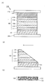
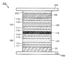
- FIGS. 1A and 1B are a schematic cross-sectional view of a light-emitting element and a schematic diagram of a light-emitting layer, to which the analysis method of one embodiment of the present invention can be applied.
- 10 is a flowchart illustrating an analysis method of one embodiment of the present invention.
- 10 is a flowchart illustrating an analysis method of one embodiment of the present invention.
- 10 is a flowchart illustrating an analysis method of one embodiment of the present invention.
- 10 is a flowchart illustrating an analysis method of one embodiment of the present invention.
- 10 is a flowchart illustrating an analysis method of one embodiment of the present invention.
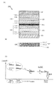
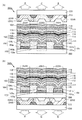
- FIG. 10 is a schematic cross-sectional view of a light-emitting element to which the analysis method of one embodiment of the present invention can be applied.
- FIG. 10 is a schematic cross-sectional view of a light-emitting element to which the analysis method of one embodiment of the present invention can be applied.
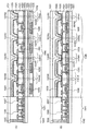
- 1 is a conceptual diagram of an active matrix light-emitting device to which an analysis method of one embodiment of the present invention can be applied.
- 1 is a conceptual diagram of an active matrix light-emitting device to which an analysis method of one embodiment of the present invention can be applied.
- FIG. 1 is a conceptual diagram of an active matrix light-emitting device to which an analysis method of one embodiment of the present invention can be applied.
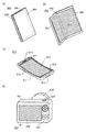
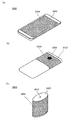
- FIG. 14 is a schematic diagram of an electronic device to which the analysis method of one embodiment of the present invention can be applied.
- FIG. 14 is a schematic diagram of an electronic device to which the analysis method of one embodiment of the present invention can be applied.
- FIG. 10 illustrates a lighting device to which the analysis method of one embodiment of the present invention can be applied.
- FIG. 10 illustrates a lighting device to which the analysis method of one embodiment of the present invention can be applied.
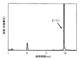
- 3A and 3B each illustrate an element structure of a light-emitting element according to an example. The figure explaining the chromatogram of LC based on an Example.
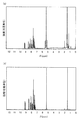
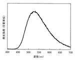
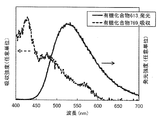
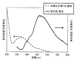
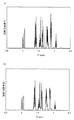
- the figure explaining the NMR spectrum of the organic compound based on an Example The figure explaining the chromatogram of LC based on an Example. The figure explaining the chromatogram of LC based on an Example. The figure explaining the NMR spectrum of the organic compound based on an Example. The figure explaining the NMR spectrum of the organic compound based on an Example. The figure explaining the NMR spectrum of the organic compound based on an Example. The figure explaining the absorption spectrum of the organic compound based on an Example. The figure explaining the emission spectrum of the organic compound based on an Example. The figure explaining the relationship between the absorption spectrum and emission spectrum of an organic compound based on an Example. The figure explaining the relationship between the absorption spectrum and emission spectrum of an organic compound based on an Example. The figure explaining the relationship between the absorption spectrum and emission spectrum of an organic compound based on an Example.
- FIG. 10 is a schematic cross-sectional view of a light-emitting element to which the analysis method of one embodiment of the present invention can be applied.
- 10 is a flowchart illustrating an analysis method of one embodiment of the present invention.
- ordinal numbers attached as the first and second are used for convenience and may not indicate the order of steps or the order of lamination. Therefore, for example, the description can be made by appropriately replacing “first” with “second” or “third”.
- the ordinal numbers described in this specification and the like may not match the ordinal numbers used to specify one embodiment of the present invention.
- the terms “film” and “layer” can be interchanged with each other.
- the term “conductive layer” may be changed to the term “conductive film”.
- the term “insulating film” may be changed to the term “insulating layer” in some cases.
- room temperature refers to a temperature in the range of 0 ° C. or higher and 40 ° C. or lower.
- the description of “near” used in the present specification to indicate the measurement value (mass-to-charge ratio; m / z) in the measurement results of ToF-SIMS or LC-MS is the presence or absence of hydrogen ions or isotope. It shows that the change of the measured value due to the presence of the body is allowed.
- the organic semiconductor element 50 has a pair of electrodes (electrode 101 and electrode 102) and the organic semiconductor layer 20.
- the organic semiconductor layer 20 may have a plurality of functional layers.
- the organic semiconductor layer 20 When the organic semiconductor layer 20 is manufactured, a thin film made of an organic compound is formed by applying a load such as heat treatment or dissolution in a solvent to the organic compound. At this time, a change such as decomposition may occur in the organic compound due to a load during film formation. Therefore, the state of the organic compound before forming the EL layer may be different from the state of the organic compound after forming the film.
- the organic semiconductor layer 20 greatly affects the characteristics of the organic semiconductor element 50. It is important that it can be manufactured.
- Analyzing the layer structure and organic compound of the organic semiconductor layer 20 includes the state of the organic compound before and after film formation, the presence or absence of decomposition products and impurities, the structure of the organic compound, the function of each layer of the EL layer, etc. Since various information can be obtained, it is useful. However, the thickness of the organic semiconductor layer in FIG. 1 is very thin, about several nanometers to several um, and each layer is made of an organic substance, so that it is difficult to analyze with a microscope. It was very difficult to analyze whether or not an organic semiconductor layer having such a structure was produced and what layer structure it had.
- the present inventors set the mass-to-charge ratio of the organic compound contained in each layer and the layered structure of the exposed organic semiconductor layer 20 as the first mass and the step of peeling either the electrode 101 or the electrode 102.
- a step of analyzing by an analysis method a step of eluting at least one or a plurality of organic compounds contained in each layer of the organic semiconductor layer 20 into a solvent to prepare a solution, and an organic compound contained in the solution by liquid chromatography.
- the step of detecting the mass-to-charge ratio of the organic compound isolated and isolated by the second mass spectrometry, the mass-to-charge ratio detected by the first mass spectrometry, and the mass-to-charge ratio detected by the second mass spectrometry And analyzing the organic semiconductor layer in which the isolated organic compound is contained, and measuring the physical properties of the isolated organic compound. It found that can analyze organic compound contained in the layer structure and each of the conductor elements.
- the TOF-SIMS method can be suitably used for the first mass spectrometry.
- the GCIB-TOF-SIMS analysis uses ion sputtering, and allows MS analysis while etching the surface. That is, since the MS analysis in the depth direction of the organic semiconductor layer is possible, the GCIB-TOF-SIMS analysis can be suitably used for the analysis of the laminated structure.
- the mass to charge ratio of the organic compound contained in each layer of the organic semiconductor layer can be obtained, and the mixed state of the organic compound contained in each layer can be analyzed.
- the organic semiconductor layer is cut in an oblique direction as viewed from the direction in which the organic semiconductor layer is laminated, as shown in FIG.
- a MALDI-TOF-MS analysis method can be used.
- the total film thickness of the organic semiconductor layer is preferably 100 nm or more and 1 ⁇ m or less.
- the area of the organic semiconductor element is preferably 4 mm 2 or more and 100 cm 2 or less.
- sample preparation under anaerobic conditions is facilitated, and it is preferable to perform sample preparation under anaerobic conditions because it is possible to obtain more accurate analysis results.
- TOF-SIMS and MALDI-TOF-MS analysis and preparation of the above-mentioned solution can be easily performed.
- the area of the organic semiconductor element exceeds 100 cm 2 , it is preferable to perform analysis after processing the organic semiconductor element to 4 mm 2 or more and 100 cm 2 or less.
- the organic semiconductor layer preferably has a weight per unit area of 1 ⁇ g / cm 2 to 100 ⁇ g / cm 2 and the semiconductor element layer has a weight of 0.04 ⁇ g to 1 mg.
- the analysis method according to one embodiment of the present invention can perform analysis even when the amount of the sample is very small.
- analysis can be performed from one smartphone size panel.
- Analysis can also be performed from a test piece size sample.
- ⁇ Configuration example 2 of organic semiconductor element> As an analysis example of the organic semiconductor element, a light-emitting element 150 shown in FIG.
- the light-emitting element 150 includes a pair of substrates (a substrate 200 and a substrate 210), a pair of electrodes (an electrode 101 and an electrode 102), and an EL layer 100 provided between the pair of electrodes.
- the EL layer 100 includes at least a light emitting layer 130.
- the EL layer 100 illustrated in FIG. 2A includes functional layers such as a hole-injection layer 111, a hole-transport layer 112, an electron-transport layer 118, and an electron-injection layer 119.
- the electrode 101 is an anode and the electrode 102 is a cathode of the pair of electrodes, but the structure of the light-emitting element 150 is not limited thereto. That is, the electrode 101 may be a cathode, the electrode 102 may be an anode, and the layers stacked between the electrodes may be reversed. That is, from the anode side, the hole injection layer 111, the hole transport layer 112, the light emitting layer 130, the electron transport layer 118, and the electron injection layer 119 may be stacked.
- the structure of the EL layer 100 is not limited to the structure illustrated in FIG. 2A, and includes at least the light-emitting layer 130, the hole-injection layer 111, the hole-transport layer 112, the electron-transport layer 118, and the electron-injection Each of the layers 119 may or may not be included.
- the EL layer 100 can reduce the hole or electron injection barrier, improve the hole or electron transport property, inhibit the hole or electron transport property, or suppress the quenching phenomenon caused by the electrode. It is good also as a structure which has a functional layer which has a function of being able to suppress child diffusion. Note that each functional layer may be a single layer or a structure in which a plurality of layers are stacked.
- the light-emitting layer 130 may include an organic compound 132 (host material) and a light-emitting material 131 (guest material).
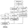
- FIG. 3 is a flowchart illustrating main processing of the purification method of one embodiment of the present invention.
- the substrate 210 which is one substrate of the light-emitting element 150 which is an analysis target is peeled off (see FIG. 3 (S1)). By peeling off the substrate 210, the one electrode 102 and the EL layer 100 are exposed. There is no particular limitation on the method for peeling the substrate 210, and the substrate can be peeled off by a physical force by triggering the sealing material with a laser or a blade.
- one electrode is peeled. (See FIG. 3 (S2)).
- the adhesive tape is preferably a tape that generates less dust, and a polyimide tape can be suitably used.
- GCIB-TOF-SIMS analysis is performed as the first mass analysis
- GCIB is preferably used for the EL layer 100, but GCIB is unsuitable for sputtering the electrode 102 which is an inorganic substance.
- a sputter ion gun different from GCIB. Measurement can be easily performed by performing TOF-SIMS analysis after the electrode 102 is peeled off.
- Argon gas is preferably used for GCIB.
- the substrate 210 and the electrode 102 are peeled, and the exposed EL layer 100 is cut obliquely, whereby each layer included in the EL layer can be exposed to the outermost surface. Therefore, the layer structure of the EL layer can be analyzed by performing TOF-SIMS analysis or MALDI-TOF-MS analysis after oblique cutting.
- GCIB-TOF-SIMS analysis can measure the mass-to-charge ratio of an organic compound with respect to the depth direction of the EL layer. For example, when GCIB-TOF-SIMS analysis is performed on the light-emitting element 150 illustrated in FIG. 2 from the electron injection layer 119 side, an organic compound contained in the electron injection layer 119 is detected first, followed by the electron transport layer 118 and the light-emitting layer.
- the stack structure of the EL layer 100 can be analyzed by analyzing the order of the obtained mass-to-charge ratio. Therefore, by performing GCIB-TOF-SIMS analysis, the stacked structure of the EL layer 100 and the organic compound contained in each layer and the mixed state of the organic compound can be analyzed. Note that GCIB-TOF-SIMS analysis is preferable because measurement can be performed by removing one electrode without performing oblique cutting described later.
- FIG. 2B after oblique cutting, for example, when TOF-SIMS analysis or MALDI-TOF-MS analysis is performed while scanning in the direction indicated by the arrow, the organic compound contained in the hole injection layer 111 is first detected. Subsequently, the mass-to-charge ratio of the organic compound contained in each of the hole transport layer 112, the light emitting layer 130, the electron transport layer 118, the electron injection layer 119, and the organic compound contained in each layer is detected. In other words, the stack structure of the EL layer 100 can be analyzed by analyzing the order of the obtained mass-to-charge ratio. Therefore, by performing GCIB-TOF-SIMS analysis, the stacked structure of the EL layer 100 and the organic compound contained in each layer and the mixed state of the organic compound can be analyzed.
- GCIB-TOF-SIMS analysis can be measured in a small amount, and it can be measured non-destructively except a portion irradiated with sputter ions.
- TOF-SIMS analysis and MALDI-TOF-MS analysis after oblique cutting can be measured in a small amount, and non-destructive measurement can be performed except for the scanned portion. Therefore, as shown by a broken line in FIG. 3, the sample subjected to the first mass spectrometry can be used in the step shown in FIG. 3 (S4). It is preferable to perform the measurement in such a procedure because the organic compound contained in the EL layer 100 can be efficiently analyzed even when the amount of the sample is small.
- a solution in which the EL layer 100 is dissolved in a desired solvent is manufactured using the sample from which the substrate 210 of the light-emitting element is peeled (the process in FIG. 3 (S1) is completed) (see FIG. 3 (S4)).
- the process in FIG. 3 (S1) is completed
- the organic compound is separated from the solution by subsequent liquid chromatography (see FIG. 3 (S5))
- substances other than the EL layer such as electrodes used in the light-emitting element 150 are mixed in the mixed solution. May be. That is, it is not necessary to dissolve only the EL layer 100 included in the light emitting element.
- the step of FIG. 3 (S5) is performed, the solution can be easily manufactured (FIG. 3 (S4)).
- the sample used in the step of FIG. 3 (S3) can also be used in the step of FIG. 3 (S4).
- the solvent used for preparation of the solution is preferably an organic solvent, and is acetone, toluene, ethyl acetate, acetonitrile, ethanol, methanol, dimethyl sulfoxide (abbreviation: DMSO), N, N-dimethyl.
- DMSO dimethyl sulfoxide
- DMF dimethyl sulfoxide
- NMP N-methyl-2-pyrrolidinone
- a chlorine-containing organic solvent such as dichloromethane, chloroform and carbon tetrachloride is more preferable.
- a chlorine-containing organic solvent is preferable because it dissolves an organic compound well and can dissolve many EL layers 100 with a small amount of solvent.
- the solvent which can be used is not limited above.
- NMR measurement described later can be performed after the production of the solution (FIG. 3 (S4)).
- Information for separating the organic compound can be obtained in the subsequent step of FIG. 3 (S5) by performing the NMR measurement. Further, by performing NMR measurement, the mixing ratio (molar ratio) of the organic compounds can be analyzed in a layer in which a plurality of organic compounds described later are mixed.
- the organic compound contained in the solution prepared in the step of FIG. 3 (S4) is separated by liquid chromatography (see FIG. 3 (S5)).
- each organic compound is isolated in this step. If isolation by a single liquid chromatography is not possible, this step may be performed multiple times.
- HPLC High Performance liquid chromatography
- Separation can be easily performed even when the amount of sample is small by using an HPLC apparatus. Further, since the HPLC apparatus and the subsequent MS apparatus and the apparatus for fractionation can be connected, the steps of FIG. 3 (S5) and FIG. 3 (S6) and the steps of FIG. 3 (S5) and FIG. 3 (S7) are performed. Can be performed continuously. The above configuration is preferable because separation and purification of the organic compound can be performed efficiently.
- second mass analysis that is, mass analysis of the isolated organic compound is performed (see FIG. 3 (S6)).
- a mass-to-charge ratio (see FIG. 3 (D2)) derived from each isolated organic compound can be obtained.
- FIG. 3 (D2) mass-to-charge ratio derived from each isolated organic compound
- FIG. 3 (D2) mass-to-charge ratio derived from each isolated organic compound
- FIG. 3 (D2) mass-to-charge ratio derived from each isolated organic compound
- the composition formula of the isolated organic compound can be analyzed. Note that the mass-to-charge ratio value detected up to the fourth decimal place may be referred to as precise mass.
- LC-MS analysis is preferably performed. As described above, since LC-MS analysis can continuously perform the steps of FIG. 3 (S5) and FIG. 3 (S6), separation and purification can be performed efficiently. An LC-MS apparatus is also preferable because an apparatus for separating separated organic compounds can be connected.
- MS / MS measurement it is preferable to perform MS / MS measurement in the step of FIG. 3 (S6). Since the mass-to-charge ratio derived from the fragment of the organic compound can be obtained by performing MS / MS measurement, the structure, substituents, and composition formula of the organic compound contained in the EL layer can be estimated.
- the organic compound isolated in FIG. 3 (S5) is collected (see FIG. 3 (S7)).
- an isolated organic compound see FIG. 3 (M1)
- NMR measurement optical measurement such as emission characteristics, absorption characteristics, and emission lifetime characteristics
- T1 triplet excitation
- Various physical properties such as level measurement and thermophysical property measurement can be performed.
- the mass-load ratio and layer structure data obtained by the first mass analysis (see FIG. 3 (D1))
- the mass-to-charge ratio (see FIG. 3D2) of the isolated organic compound obtained from the second mass measurement the layer in which the isolated organic compound (M1) is in the EL layer 100 Can be analyzed (see FIG. 3 (S8)).
- the mixing ratio of the organic compounds may be important.
- the light emitting layer includes a host material and a guest material, and the mixing ratio of the host material and the guest material is important for the light emission characteristics.
- 1 H-NMR measurement of each organic compound contained in the same layer fractionated by the above-mentioned steps is performed, and the NMR spectrum obtained before isolation and the 1 H-NMR spectrum of the organic compound after isolation By comparing these, the molar ratio of a plurality of organic compounds contained in the same layer can be calculated.
- the structure and physical properties of the organic compound, the function of each layer, and the like can be analyzed.
- the state of the substance before and after film formation can be known. Therefore, it is possible to analyze the presence or absence of decomposition products and impurities, and it is possible to analyze the characteristics of the light emitting element.
- the light emission mechanism can be analyzed by analyzing the optical characteristics of the organic compound contained in the light emitting layer. Further, by knowing the mixed state of each layer, the physical properties of the mixed state can be measured.
- the physical property value of the mixed film at the same mixing ratio can be accurately known. Since there is information that becomes apparent for the first time by analyzing the element after fabrication, according to one embodiment of the present invention, new information that cannot be read from the design drawing of the element can be obtained.
- analysis of the light-emitting element shows an analysis example of a light-emitting element with a known element structure
- the analysis method according to one embodiment of the present invention is not limited thereto. That is, the present invention can be applied to an organic semiconductor element and a light emitting element whose structure is unknown, and a layer structure and an organic compound included in the element can be analyzed.
- the analysis method according to one embodiment of the present invention can also be preferably used for an organic photoelectric conversion element such as an organic solar cell or an organic photodiode.
- the analysis method according to one embodiment of the present invention is not limited thereto. That is.
- the analysis method according to one embodiment of the present invention can also be applied to an organic semiconductor element made of a single organic compound.
- FIG. 4 is a flowchart of an organic compound analysis method according to one embodiment of the present invention.
- NMR measurement of the organic compound A isolated in FIG. 3 (M1) is performed (see FIG. 4 (S9)), and an NMR spectrum of the organic compound A (see FIG. 4 (D3)) is obtained.
- This NMR measurement is preferably performed for at least 1 H.
- it is preferable to perform 13 C or two-dimensional NMR measurement because molecular structure analysis can be performed in more detail. Further, the molecular structure analysis can be performed in more detail by measuring the melting point and the optical rotation in the step of FIG. 4 (S9).
- the organic compound B having the estimated molecular structure is actually synthesized (see FIG. 4 (S11)).
- synthesis method and the synthesis route There are no particular limitations on the synthesis method and the synthesis route, and various synthesis methods such as Suzuki-Miyaura coupling reaction, Buchwald-Hartwig reaction, Ullmann reaction and the like can be used.
- the organic compound B since it is a process of obtaining the organic compound B, when the organic compound B is marketed, it may replace with the process of (S11) and may purchase a commercial item, and the organic compound B Is the organic compound used in manufacturing the light-emitting element 150, and when there is knowledge of the molecular structure, the organic compound used in manufacturing the light-emitting element 150 may be used in the step (S12) described below.
- NMR of the synthesized organic compound B is measured (see FIG. 4 (S12)), and an NMR spectrum of the organic compound B (see FIG. 4 (D4)) is obtained.
- This NMR measurement is preferably performed for at least 1 H.
- it is preferable to perform 13 C or two-dimensional NMR measurement because molecular structure analysis can be performed in more detail. Further, more detailed molecular structure analysis can be performed by performing optical rotation measurement and MS measurement in the step of FIG. 4 (S9).
- the molecular structure of the organic compound A is identified by comparing D3 and D4. If the intensity ratio and peak position of each peak of D3 and D4 match, it can be said that the molecular structure of the organic compound A has the same structure as the estimated organic compound B. At this time, the accuracy of analysis can be improved by simultaneously analyzing data other than NMR.
- the molecular structure of the identified organic compound A with the structure of the organic compound used in manufacturing the light-emitting element 150, it can be confirmed whether or not the target substance can be formed in the target layer.
- the characteristics of the light-emitting element can be analyzed in detail by specifying the molecular structure.
- the structure of the organic compound contained in an unknown light emitting element can be identified by performing the said analysis method similarly to an unknown light emitting element.
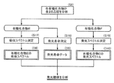
- FIG. 5 is a flowchart of an analysis method for analyzing whether an exciplex (also referred to as an exciplex) is generated between organic compounds used in the light-emitting element which is one embodiment of the present invention.
- an exciplex also referred to as an exciplex
- the layer containing the organic compound C and the organic compound D presumed to be interacting is specified by performing the process of FIG. 3 (S7).
- S7 the process of FIG. 3
- emission spectrum data shown in FIGS. 5 (D5) and (D6) are obtained by measuring respective emission spectra of the organic compound C and the organic compound D (see FIGS. 5 (S13) and (S14)). .
- the above emission spectrum may be measured in a state where each organic compound is in a solution state or a thin film state, but it is preferable that each organic compound is measured in the same state.
- a mixture of the organic compound C and the organic compound D is prepared (see FIG. 5 (S15)).
- the state of the mixture may be a solution state or a thin film state, it is preferable to prepare a mixed film in the same state as the state where the emission spectrum of each organic compound is measured.
- Thin film production methods include vacuum deposition and wet processes (spin coating method, casting method, die coating method, blade coating method, roll coating method, ink jet method, printing method, spray coating method, curtain coating method, Langmuir-Blodgett method, etc.) Can be used.
- the emission spectrum data of the mixture shown in FIG. 5 (D7) is obtained by measuring the emission spectrum of the prepared mixture (see FIG. 5 (S16)).
- FIG. 6 is a flowchart of an analysis method relating to a light-emitting mechanism of a light-emitting element, which is one embodiment of the present invention. Note that in the first mass spectrometry (FIG. 3 (S3)), when mass-to-charge ratios of a plurality of types of organic compounds are obtained from the same layer, the layer may be estimated as a light-emitting layer.
- the organic compound E and the organic compound F estimated to be contained in the light emitting layer are analyzed in detail by performing the process of FIG. 3 (S7).
- the organic compound E is described as a guest material in the light emitting layer
- the organic compound F is described as a host material.
- an organic compound having a heavy atom such as Ir is used for the light-emitting layer at the time of manufacturing the light-emitting element, or by analyzing the isotope peak of the heavy atom in TOF-SIMS analysis
- the guest material can be specified.
- an organic compound having a low relative ion intensity detected in TOF-SIMS analysis (FIG. 3 (S3)) is assumed to be a guest material, and the other is assumed to be a host material. Also good.
- the absorption spectrum data of the organic compound E shown in FIG. 6 (D8) is obtained by measuring the absorption spectrum of the organic compound E (see FIG. 6 (S17)).
- the emission lifetime of the organic compound E is analyzed by measuring the emission lifetime of the organic compound E (see FIG. 6 (S18)) and analyzing the emission lifetime data of the organic compound E shown in FIG. 6 (D9).
- the emission lifetime is on the nanosecond scale, it can be interpreted as fluorescence emission, and when the decay curve can be expressed by a linear expression, it can be interpreted as phosphorescence emission.
- the decay curve of the luminescence lifetime can be expressed by a relational expression of second order or higher, it can be analyzed that it has a delayed luminescence component (typically a thermally activated delayed fluorescence component).
- the emission spectrum data shown in FIG. 6 (D10) is obtained by measuring the emission spectrum of the organic compound F in the same manner as in FIGS. 5 (S13) and (S14) (see FIG. 6 (S19)).
- the light emission mechanism in the light emitting element can be analyzed.
- the light emission characteristics of the organic compound E can be analyzed from (D9).
- knowledge about energy transfer from the organic compound F as the host material to the organic compound E as the guest material can be obtained.
- this analysis can be applied to a light-emitting element whose element structure is unknown.
- FIG. 7 is a flowchart of an analysis method relating to a light-emitting mechanism of a light-emitting element, which is one embodiment of the present invention.
- the organic compound G and the organic compound H will be described as a host material
- the organic compound I will be described as a guest material.
- the organic compound having the lowest relative intensity of the ionic strength detected in the first mass analysis (FIG. 3 (S3)) is estimated as the guest material, and the other is estimated as the host material. You may do it.
- Steps (S20) to (S23) in FIG. 7 are the same as steps (S13) to (S16) in FIG.
- the organic compound G and the organic compound H form an exciplex in the light emitting layer, similarly to the data analysis of (D5) to (D7) in FIG. You can analyze what to do.
- the steps (S24) and (S25) in FIG. 7 are the same as the steps (S17) and (S18) in FIG.
- the light emission characteristics of the organic compound I can be analyzed.
- the light emission mechanism of the light emitting element can be analyzed.
- the organic compound G and the organic compound H form an exciplex and the organic compound I emits phosphorescence from the above analysis
- the overlap of the absorption spectrum shown in (D14) and the emission spectrum shown in (D12) is analyzed. It is possible to analyze whether or not ExTET (Exciplex Triplet Energy Transfer) described later is generated in the light emitting layer.
- ExTET Extraplex Triplet Energy Transfer
- the organic compound 132 is present in the largest amount by weight, and the light emitting material 131 is dispersed in the organic compound 132.
- the S1 level of the organic compound 132 of the light-emitting layer 130 is preferably higher than the S1 level of the light-emitting material of the light-emitting layer 130 (light-emitting material 131).
- the T1 level of the organic compound 132 in the light-emitting layer 130 is preferably higher than the T1 level of the light-emitting material (the light-emitting material 131) in the light-emitting layer 130.
- the organic compound 132 is preferably a compound having a nitrogen-containing six-membered heteroaromatic skeleton.
- the compound having a basic nitrogen-containing heteroaromatic skeleton include compounds having a pyridine skeleton, a diazine skeleton (pyrazine skeleton, pyrimidine skeleton, and pyridazine skeleton), and a triazine skeleton. Examples include pyridine derivatives, bipyridine derivatives, pyrimidine derivatives, triazine derivatives, quinoxaline derivatives, dibenzoquinoxaline derivatives, phenanthroline derivatives, and purine derivatives.
- a material having an electron transport property higher than that of holes can be used, and the material has an electron mobility of 1 ⁇ 10 ⁇ 6 cm 2 / Vs or more. It is preferable.
- heterocyclic compounds having a pyridine skeleton such as bathophenanthroline (abbreviation: BPhen), bathocuproin (abbreviation: BCP), and 2- [3- (dibenzothiophen-4-yl) phenyl] dibenzo [f , H] quinoxaline (abbreviation: 2mDBTPDBq-II), 2- [3 ′-(dibenzothiophen-4-yl) biphenyl-3-yl] dibenzo [f, h] quinoxaline (abbreviation: 2mDBTPBPDBq-II), 2- [ 3 ′-(9H-carbazol-9-yl) biphenyl-3-yl] dibenzo [f, h] quinoxaline (abbreviation: 2mCzBPDBq), 2- [4- (3,6-diphenyl-9H-carbazol-9-yl) ) Phenyl] dibenzo [f, h] quinoxaline (abb
- heterocyclic compound having a triazine skeleton, a diazine (pyrimidine, pyrazine, pyridazine) skeleton, or a pyridine skeleton is preferable because it is stable and reliable.
- the heterocyclic compound having the skeleton has a high electron transporting property and contributes to a reduction in driving voltage.
- poly (2,5-pyridinediyl) (abbreviation: PPy), poly [(9,9-dihexylfluorene-2,7-diyl) -co- (pyridine-3,5-diyl)] (abbreviation: PF -Py), poly [(9,9-dioctylfluorene-2,7-diyl) -co- (2,2′-bipyridine-6,6′-diyl)] (abbreviation: PF-BPy) Molecular compounds can also be used.
- the substances mentioned here are mainly substances having an electron mobility of 1 ⁇ 10 ⁇ 6 cm 2 / Vs or higher. Note that other than the above substances, any substance that has a property of transporting more electrons than holes may be used.
- a compound having a nitrogen-containing five-membered heterocyclic skeleton or a tertiary amine skeleton can also be suitably used.
- Specific examples include a pyrrole skeleton or an aromatic amine skeleton.
- indole derivatives, carbazole derivatives, triarylamine derivatives, and the like can be given.
- the nitrogen-containing five-membered heterocyclic skeleton include an imidazole skeleton, a triazole skeleton, and a tetrazole skeleton.
- the organic compound 132 a material having a property of transporting more holes than electrons (a hole transporting material) can be used, and a material having a hole mobility of 1 ⁇ 10 ⁇ 6 cm 2 / Vs or more. It is preferable that The hole transporting material may be a polymer compound.
- N, N′-di (p-tolyl) -N, N′-diphenyl-p-phenylenediamine (abbreviation: DTDPPA) 4,4′-bis [N- (4-diphenylaminophenyl) -N-phenylamino] biphenyl (abbreviation: DPAB)
- N, N′-bis ⁇ 4- [bis (3-methylphenyl) amino] phenyl ⁇ -N, N′-diphenyl- (1,1′-biphenyl) -4,4′-diamine (abbreviation: DNTPD), 1,3,5-tris [N- (4-diphenylaminophenyl) -N— Phenylamino] benzene (abbreviation: DPA3B) and the like.
- PCzDPA1 3- [N- (4-diphenylaminophenyl) -N-phenylamino] -9-phenylcarbazole
- PCzDPA2 3,6-bis [N- ( 4-diphenylaminophenyl) -N-phenylamino] -9-phenylcarbazole
- PCzTPN2 3,6-bis [N- (4-diphenylaminophenyl) -N- (1-naphthyl) amino] -9 -Phenylcarbazole
- PCzTPN2 3- [N- (9-phenylcarbazol-3-yl) -N-phenylamino] -9-phenylcarbazole
- PCzPCA1 3,6-bis [N- ( 9-phenylcarbazol-3-yl) -N-phenylamino] -9-phenylcarbazole
- PCzPCA1 3,6-bis [N- ( 9-phenylc
- CBP 4,4′-di (N-carbazolyl) biphenyl
- TCPB 1,3,5-tris [4- (N-carbazolyl) phenyl] benzene
- CzPA 9- [4- (10-phenyl-9-anthryl) phenyl] -9H-carbazole
- CzPA 1,4-bis [4- (N-carbazolyl) phenyl] -2,3,5, 6-tetraphenylbenzene or the like
- poly (N-vinylcarbazole) (abbreviation: PVK), poly (4-vinyltriphenylamine) (abbreviation: PVTPA), poly [N- (4- ⁇ N ′-[4- (4-diphenylamino)] Phenyl] phenyl-N′-phenylamino ⁇ phenyl) methacrylamide] (abbreviation: PTPDMA), poly [N, N′-bis (4-butylphenyl) -N, N′-bis (phenyl) benzidine] (abbreviation: Polymer compounds such as Poly-TPD can also be used.
- NPB or ⁇ -NPD 4,4′-bis [N- (1-naphthyl) -N-phenylamino] biphenyl
- NPB or ⁇ -NPD N, N′— Bis (3-methylphenyl) -N, N′-diphenyl- [1,1′-biphenyl] -4,4′-diamine
- TPD 4,4 ′, 4 ′′ -tris (carbazole-9) -Yl) triphenylamine
- TCTA 4,4 ′, 4 ′′ -tris [N- (1-naphthyl) -N-phenylamino] triphenylamine
- 1′-TNATA 4, 4 ′, 4 ′′ -tris (N, N-diphenylamino) triphenylamine
- TDATA 4,4 ′, 4 ′, 4 ′, 4 ′, 4 ′′ -tris (N, N-diphenylamino) triphenylamine
- PCPN 3- [4- (1-naphthyl) -phenyl] -9-phenyl-9H-carbazole
- PCPPn 3- [4- (9-phenanthryl) -phenyl] -9-phenyl-9H-carbazole
- PCCP 3,3′-bis (9-phenyl-9H-carbazole)
- mCP 1,3-bis (N-carbazolyl) benzene
- mCP 1,3-bis (N-carbazolyl) benzene
- CzTP 3,5-diphenylphenyl) -9-phenylcarbazole
- PhCzGI 3,6-di (9H-carbazol-9-yl) -9-phenyl-9H-carbazole
- PhCzGI 2,8- An amine compound such as di (9H-carbazol-9-yl) -dibenzothiophene
- a compound having a pyrrole skeleton or an aromatic amine skeleton is preferable because it is stable and reliable.
- the compound having the skeleton has a high hole transport property and contributes to a reduction in driving voltage.
- a compound having a nitrogen-containing five-membered heterocyclic skeleton such as an imidazole skeleton, a triazole skeleton, or a tetrazole skeleton can be used.
- a compound having a nitrogen-containing five-membered heterocyclic skeleton such as an imidazole skeleton, a triazole skeleton, or a tetrazole skeleton
- TAZ 3- (4-biphenylyl) -4-phenyl-5- (4-tert-butylphenyl) -1,2,4-triazole
- TAZ 9- [4- (4 , 5-Diphenyl-4H-1,2,4-triazol-3-yl) phenyl] -9H-carbazole
- CzTAZ1 1, 2,2 ′, 2 ′′-(1,3,5-benzenetriyl
- Tris (1-phenyl-1H-benzimidazole) (abbreviation: TPBI
- the light-emitting material 131 is not particularly limited.
- the fluorescent compound include anthracene derivatives, tetracene derivatives, chrysene derivatives, phenanthrene derivatives, pyrene derivatives, perylene derivatives, stilbene derivatives, acridone derivatives, Coumarin derivatives, phenoxazine derivatives, phenothiazine derivatives, and the like are preferable.
- the following substances can be used.
- Examples of the light-emitting material 131 include iridium, rhodium, or platinum-based organometallic complexes, or metal complexes.
- organic iridium complexes such as iridium-based orthometal complexes are preferable.
- Examples of orthometalated ligands include 4H-triazole ligands, 1H-triazole ligands, imidazole ligands, pyridine ligands, pyrimidine ligands, pyrazine ligands, and isoquinoline ligands.
- Examples of the metal complex include a platinum complex having a porphyrin ligand.
- Examples of the substance having an emission peak in the blue or green wavelength region include tris ⁇ 2- [5- (2-methylphenyl) -4- (2,6-dimethylphenyl) -4H-1,2,4- Triazol-3-yl- ⁇ N 2 ] phenyl- ⁇ C ⁇ iridium (III) (abbreviation: Ir (mppptz-dmp) 3 ), tris (5-methyl-3,4-diphenyl-4H-1,2,4-triazolate ) Iridium (III) (abbreviation: Ir (Mptz) 3 ), tris [4- (3-biphenyl) -5-isopropyl-3-phenyl-4H-1,2,4-triazolato] iridium (III) (abbreviation: Ir (iPrptz-3b) 3) , tris [3- (5-biphenyl) -5-isopropyl-4-phenyl-4H-1,2,4-triazola
- organometallic iridium complexes having a nitrogen-containing five-membered heterocyclic skeleton such as a 4H-triazole skeleton, a 1H-triazole skeleton, and an imidazole skeleton have high triplet excitation energy, and have high reliability and luminous efficiency. It is particularly preferred because of its superiority.
- Examples of the substance having an emission peak in the green or yellow wavelength region include tris (4-methyl-6-phenylpyrimidinato) iridium (III) (abbreviation: Ir (mppm) 3 ), tris (4- t-butyl-6-phenylpyrimidinato) iridium (III) (abbreviation: Ir (tBupppm) 3 ), (acetylacetonato) bis (6-methyl-4-phenylpyrimidinato) iridium (III) (abbreviation: Ir (mppm) 2 (acac)), (acetylacetonato) bis (6-tert-butyl-4-phenylpyrimidinato) iridium (III) (abbreviation: Ir (tBupppm) 2 (acac)), (acetylacetate) Nato) bis [4- (2-norbornyl) -6-phenylpyrimidinato] iridium (III) (abbreviation
- organometallic iridium complexes having a pyrimidine skeleton are particularly preferable because they are remarkably excellent in reliability and luminous efficiency.
- An organometallic iridium complex having a pyrazine skeleton can be favorably used for the light-emitting element of one embodiment of the present invention because red light emission with high chromaticity is obtained.
- the light emitting material included in the light emitting layer 130 is preferably a material that can convert triplet excitation energy into light emission.
- the material capable of converting the triplet excitation energy into light emission include a thermally activated delayed fluorescence (TADF) material in addition to a phosphorescent compound. Therefore, the portion described as a phosphorescent compound may be read as a thermally activated delayed fluorescent material.
- TADF thermally activated delayed fluorescence
- the thermally activated delayed fluorescent material has a small difference between the triplet excitation energy level and the singlet excitation energy level, and the function of converting energy from the triplet excited state to the singlet excited state by crossing between inverses. It is the material which has.
- the triplet excited state can be up-converted (reverse intersystem crossing) into a singlet excited state with a slight thermal energy, and light emission (fluorescence) from the singlet excited state can be efficiently exhibited.
- the energy difference between the triplet excitation energy level and the singlet excitation energy level is preferably greater than 0 eV but not greater than 0.2 eV, more preferably greater than 0 eV and not greater than 0. 0.1 eV or less.
- the TADF material can be used not only as a light emitting material but also as a host material of a light emitting layer.
- thermally activated delayed fluorescent material is composed of one type of material, for example, the following materials can be used.
- metal-containing porphyrins including magnesium (Mg), zinc (Zn), cadmium (Cd), tin (Sn), platinum (Pt), indium (In), palladium (Pd), and the like can be given.
- metal-containing porphyrin include a protoporphyrin-tin fluoride complex (SnF 2 (Proto IX)), a mesoporphyrin-tin fluoride complex (SnF 2 (Meso IX)), and a hematoporphyrin-tin fluoride complex (SnF).
- thermoly activated delayed fluorescent material composed of a kind of material
- a heterocyclic compound having a ⁇ -electron rich heteroaromatic ring and a ⁇ -electron deficient heteroaromatic ring can also be used.
- the heterocyclic compound has a ⁇ -electron rich heteroaromatic ring and a ⁇ -electron deficient heteroaromatic ring, it is preferable because of its high electron transporting property and hole transporting property.
- a diazine skeleton pyrimidine skeleton, pyrazine skeleton, pyridazine skeleton
- a triazine skeleton is preferable because it is stable and has high reliability.
- an acridine skeleton, a phenoxazine skeleton, a thiophene skeleton, a furan skeleton, and a pyrrole skeleton are stable and reliable. It is preferable to have one or more.
- the pyrrole skeleton an indole skeleton, a carbazole skeleton, and a 3- (9-phenyl-9H-carbazol-3-yl) -9H-carbazole skeleton are particularly preferable.
- a substance in which a ⁇ -electron rich heteroaromatic ring and a ⁇ -electron deficient heteroaromatic ring are directly bonded has both a donor property of a ⁇ -electron rich heteroaromatic ring and an acceptor property of a ⁇ -electron deficient heteroaromatic ring, This is particularly preferable because the difference between the energy level in the singlet excited state and the energy level in the triplet excited state is small.
- the light-emitting layer 130 may include a material other than the organic compound 132 and the light-emitting material 131.
- a material that can be used for the light-emitting layer 130 is not particularly limited, and examples thereof include condensed polycyclic aromatic compounds such as anthracene derivatives, phenanthrene derivatives, pyrene derivatives, chrysene derivatives, and dibenzo [g, p] chrysene derivatives.
- 9,10-diphenylanthracene (abbreviation: DPAnth), 6,12-dimethoxy-5,11-diphenylchrysene, 9,10-bis (3,5-diphenylphenyl) anthracene (abbreviation: DPPA), 9,10-di (2-naphthyl) anthracene (abbreviation: DNA), 2-tert-butyl-9,10-di (2-naphthyl) anthracene (abbreviation: t-BuDNA), 9,9′- Bianthryl (abbreviation: BANT), 9,9 ′-(stilbene-3,3′-diyl) diphenanthrene (abbreviation: DP) S), 9,9 ′-(stilbene-4,4′-diyl) diphenanthrene (abbreviation: DPNS2), 1,3,5-tri (1-pyrenyl) benzene (abbreviation: TPB3)
- a compound having a heteroaromatic skeleton such as an oxadiasol derivative can be used for the light-emitting layer 130.
- a compound having a heteroaromatic skeleton such as an oxadiasol derivative
- PBD 2- (4-biphenylyl) -5- (4-tert-butylphenyl) -1,3,4-oxadiazole
- OXD-7 1,3-bis [5- (P-tert-butylphenyl) -1,3,4-oxadiazol-2-yl] benzene
- OXD-7 1,3-bis [5- (P-tert-butylphenyl) -1,3,4-oxadiazol-2-yl] benzene
- OXD-7 1,3-bis [5- (P-tert-butylphenyl) -1,3,4-oxadiazol-2-yl] benzene
- OXD-7 1,3-bis [5- (P-tert-but
- a metal complex having a heterocyclic ring eg, zinc and aluminum-based metal complex
- a metal complex having a quinoline ligand, a benzoquinoline ligand, an oxazole ligand, or a thiazole ligand can be given.
- tris (8-quinolinolato) aluminum (III) (abbreviation: Alq)
- tris (4-methyl-8-quinolinolato) aluminum (III) abbreviation: Almq3)
- bis (10-hydroxybenzo [ h] quinolinato) beryllium (II) (abbreviation: BeBq2)
- bis (2-methyl-8-quinolinolato) (4-phenylphenolato) aluminum (III) abbreviation: BAlq
- bis (8-quinolinolato) zinc (II) ) (Abbreviation: Znq) and the like
- metal complexes having a quinoline skeleton or a benzoquinoline skeleton and metal complexes having a quinoline skeleton or a benzoquinoline skeleton.
- bis [2- (2-benzoxazolyl) phenolato] zinc (II) (abbreviation: ZnPBO), bis [2- (2-benzothiazolyl) phenolato] zinc (II) (abbreviation: ZnBTZ), etc.
- ZnPBO bis [2- (2-benzoxazolyl) phenolato] zinc
- ZnBTZ bis [2- (2-benzothiazolyl) phenolato] zinc
- a metal complex having an oxazole-based or thiazole-based ligand can also be used.
- the light-emitting layer 130 can be formed of a plurality of layers of two or more layers.
- a substance having a hole-transport property is used as the host material of the first light-emitting layer
- a substance having an electron transporting property is used as a host material of the second light emitting layer.
- the light-emitting materials included in the first light-emitting layer and the second light-emitting layer may be the same material or different materials, and may be different materials that have a function of emitting light of the same color.
- a material having a function of emitting light of a color may be used.
- a light emitting material having a function of emitting light of different colors for each of the two light emitting layers, a plurality of light emissions can be obtained simultaneously.
- the light-emitting layer 130 can be formed by a method such as a vapor deposition method (including a vacuum vapor deposition method), an inkjet method, a coating method, or gravure printing. Further, in addition to the materials described above, an inorganic compound such as a quantum dot or a polymer compound (oligomer, dendrimer, polymer, etc.) may be included.
- the hole injection layer 111 has a function of promoting hole injection by reducing a hole injection barrier at the interface between the hole injection layer 111 and one of the pair of electrodes (the electrode 101 or the electrode 102). It is formed by a product, a phthalocyanine derivative, or an aromatic amine.
- the transition metal oxide include molybdenum oxide, vanadium oxide, ruthenium oxide, tungsten oxide, and manganese oxide.
- the phthalocyanine derivative include phthalocyanine and metal phthalocyanine.
- aromatic amines include benzidine derivatives and phenylenediamine derivatives. High molecular compounds such as polythiophene and polyaniline can also be used. For example, self-doped polythiophene poly (ethylenedioxythiophene) / poly (styrenesulfonic acid) is a typical example.
- a layer including a composite material of a hole-transporting material and a material that exhibits an electron-accepting property can be used.
- a stack of a layer containing a material showing an electron accepting property and a layer containing a hole transporting material may be used. Charges can be transferred between these materials in a steady state or in the presence of an electric field.
- the material exhibiting electron acceptability include organic acceptors such as quinodimethane derivatives, chloranil derivatives, and hexaazatriphenylene derivatives.
- F4-TCNQ 7,7,8,8-tetracyano-2,3,5,6-tetrafluoroquinodimethane
- chloranil 2,3,6,7,10,11- A compound having an electron withdrawing group (halogen group or cyano group) such as hexacyano-1,4,5,8,9,12-hexaazatriphenylene (abbreviation: HAT-CN).
- Transition metal oxides such as Group 4 to Group 8 metal oxides can also be used.
- molybdenum oxide is preferable because it is stable in the air, has a low hygroscopic property, and is easy to handle.
- transport material having high hole is preferably a material having a 1 ⁇ 10 -6 cm 2 / Vs or more hole mobility.
- aromatic amines, carbazole derivatives, aromatic hydrocarbons, stilbene derivatives, and the like which are listed as hole transporting materials that can be used for the light-emitting layer 130 can be used.
- the hole transporting material may be a polymer compound.
- hole transporting material examples include aromatic hydrocarbons, such as 2-tert-butyl-9,10-di (2-naphthyl) anthracene (abbreviation: t-BuDNA), 2-tert- Butyl-9,10-di (1-naphthyl) anthracene, 9,10-bis (3,5-diphenylphenyl) anthracene (abbreviation: DPPA), 2-tert-butyl-9,10-bis (4-phenylphenyl) ) Anthracene (abbreviation: t-BuDBA), 9,10-di (2-naphthyl) anthracene (abbreviation: DNA), 9,10-diphenylanthracene (abbreviation: DPAnth), 2-tert-butylanthracene (abbreviation: t-) BuAnth), 9,10-bis (4-methyl-1-naphthyl) anthracene
- pentacene, coronene, and the like can also be used.
- an aromatic hydrocarbon having a hole mobility of 1 ⁇ 10 ⁇ 6 cm 2 / Vs or more and having 14 to 42 carbon atoms.
- the aromatic hydrocarbon may have a vinyl skeleton.
- the aromatic hydrocarbon having a vinyl group for example, 4,4′-bis (2,2-diphenylvinyl) biphenyl (abbreviation: DPVBi), 9,10-bis [4- (2,2- Diphenylvinyl) phenyl] anthracene (abbreviation: DPVPA) and the like.
- a compound having a pyrrole skeleton, a furan skeleton, a thiophene skeleton, or an aromatic amine skeleton is preferable because it is stable and reliable.
- the compound having the skeleton has a high hole transport property and contributes to a reduction in driving voltage.
- the hole transport layer 112 is a layer containing a hole transport material, and the hole transport material exemplified as the material of the hole injection layer 111 can be used. Since the hole transport layer 112 has a function of transporting holes injected into the hole injection layer 111 to the light emitting layer 130, the HOMO (High Occupied Molecular Orbital) of the hole injection layer 111 is also known. It is preferable to have a HOMO level that is the same as or close to the position.
- a substance having a hole mobility of 1 ⁇ 10 ⁇ 6 cm 2 / Vs or higher is preferable.
- any substance other than these may be used as long as it has a property of transporting more holes than electrons.
- the layer containing a substance having a high hole-transport property is not limited to a single layer, and two or more layers containing the above substances may be stacked.
- the electron transport layer 118 has a function of transporting electrons injected from the other of the pair of electrodes (the electrode 101 or the electrode 102) through the electron injection layer 119 to the light emitting layer 130.
- the electron transporting material a material having a higher electron transporting property than holes can be used, and a material having an electron mobility of 1 ⁇ 10 ⁇ 6 cm 2 / Vs or more is preferable.
- a compound that easily receives electrons (a material having an electron transporting property)
- a ⁇ -electron deficient heteroaromatic such as a nitrogen-containing heteroaromatic compound, a metal complex, or the like can be used.
- the pyridine derivatives, bipyridine derivatives, pyrimidine derivatives, triazine derivatives, quinoxaline derivatives, dibenzoquinoxaline derivatives, phenanthroline derivatives, triazole derivatives, benzimidazole derivatives, oxalates which are listed as electron transporting materials that can be used for the light-emitting layer 130.
- diazole derivatives a substance having an electron mobility of 1 ⁇ 10 ⁇ 6 cm 2 / Vs or higher is preferable.
- any substance that has a property of transporting more electrons than holes may be used for the electron-transport layer.
- the electron-transporting layer 118 is not limited to a single layer, and two or more layers including the above substances may be stacked.
- the metal complex which has a heterocyclic ring is mentioned,
- the metal complex which has a quinoline ligand, a benzoquinoline ligand, an oxazole ligand, or a thiazole ligand is mentioned.
- tris (8-quinolinolato) aluminum (III) (abbreviation: Alq)
- tris (4-methyl-8-quinolinolato) aluminum (III) abbreviation: Almq3)
- bis (10-hydroxybenzo [ h] quinolinato) beryllium (II) (abbreviation: BeBq2)
- bis (2-methyl-8-quinolinolato) (4-phenylphenolato) aluminum (III) abbreviation: BAlq
- bis (8-quinolinolato) zinc (II) ) (Abbreviation: Znq) and the like
- metal complexes having a quinoline skeleton or a benzoquinoline skeleton and metal complexes having a quinoline skeleton or a benzoquinoline skeleton.
- bis [2- (2-benzoxazolyl) phenolato] zinc (II) (abbreviation: ZnPBO), bis [2- (2-benzothiazolyl) phenolato] zinc (II) (abbreviation: ZnBTZ), etc.
- ZnPBO bis [2- (2-benzoxazolyl) phenolato] zinc
- ZnBTZ bis [2- (2-benzothiazolyl) phenolato] zinc
- a metal complex having an oxazole-based or thiazole-based ligand can also be used.
- a layer for controlling the movement of electron carriers may be provided between the electron transport layer 118 and the light emitting layer 130.
- This is a layer obtained by adding a small amount of a substance having a high electron trapping property to a material having a high electron transporting property as described above. By suppressing the movement of electron carriers, the carrier balance can be adjusted.
- Such a configuration is highly effective in suppressing problems that occur when the electron transporting property of the electron transporting material is significantly higher than the hole transporting property of the hole transporting material (for example, a reduction in device lifetime). .
- the electron injection layer 119 has a function of promoting electron injection by reducing an electron injection barrier at the interface between the electron injection layer 119 and the electrode 102.
- a group 1 metal, a group 2 metal, or an oxide thereof Halides, carbonates and the like can be used.
- a composite material of the electron transporting material described above and a material exhibiting an electron donating property can be used. Examples of the material exhibiting electron donating properties include Group 1 metals, Group 2 metals, and oxides thereof.
- alkali metals and alkaline earth metals such as lithium fluoride (LiF), sodium fluoride (NaF), cesium fluoride (CsF), calcium fluoride (CaF2), lithium oxide (LiOx), etc. Or a compound thereof.
- a rare earth metal compound such as erbium fluoride (ErF3) can be used.
- electride may be used for the electron injection layer 119. Examples of the electride include a substance obtained by adding a high concentration of electrons to a mixed oxide of calcium and aluminum. Alternatively, a substance that can be used for the electron-transport layer 118 may be used for the electron-injection layer 119.
- a composite material obtained by mixing an organic compound and an electron donor (donor) may be used for the electron injection layer 119.
- Such a composite material is excellent in electron injecting property and electron transporting property because electrons are generated in the organic compound by the electron donor.
- the organic compound is preferably a material excellent in transporting the generated electrons.
- a substance (metal complex, heteroaromatic compound, or the like) constituting the electron transport layer 118 described above is used.
- the electron donor may be any substance that exhibits an electron donating property to the organic compound.
- an alkali metal, an alkaline earth metal, or a rare earth metal is preferable, and examples thereof include lithium, sodium, cesium, magnesium, calcium, erbium, and ytterbium.
- Alkali metal oxides and alkaline earth metal oxides are preferable, and lithium oxide, calcium oxide, barium oxide, and the like can be given.
- a Lewis base such as magnesium oxide can also be used.
- an organic compound such as tetrathiafulvalene (abbreviation: TTF) can be used.
- the light emitting layer, the hole injection layer, the hole transport layer, the electron transport layer, and the electron injection layer described above are formed by a vapor deposition method (including a vacuum vapor deposition method), an inkjet method, a coating method, a gravure printing, and the like, respectively. Can be formed by a method.
- the light emitting layer, hole injection layer, hole transport layer, electron transport layer, and electron injection layer described above include inorganic compounds such as quantum dots, and polymer compounds (oligomers, dendrimers). , Polymers, etc.) may be used.
- a quantum dot is a semiconductor nanocrystal having a size of several nanometers to several tens of nanometers, and is composed of about 1 ⁇ 10 3 to 1 ⁇ 10 6 atoms. Since quantum dots shift in energy depending on the size, even if the quantum dots are made of the same material, the emission wavelength differs depending on the size. Therefore, the emission wavelength can be easily changed by changing the size of the quantum dots to be used.
- quantum dots since the quantum dot has a narrow emission spectrum peak width, light emission with good color purity can be obtained. Furthermore, the theoretical internal quantum efficiency of quantum dots is said to be almost 100%, which is much higher than 25% of organic compounds that exhibit fluorescence and is equivalent to organic compounds that exhibit phosphorescence. For this reason, a light-emitting element with high emission efficiency can be obtained by using quantum dots as a light-emitting material. In addition, quantum dots, which are inorganic materials, are excellent in essential stability, and thus a light-emitting element that is preferable from the viewpoint of life can be obtained.
- the materials constituting the quantum dots include group 14 elements, group 15 elements, group 16 elements, compounds composed of a plurality of group 14 elements, elements belonging to groups 4 to 14 and group 16 elements.
- Compounds of Group 2, elements of Group 16 and Group 16, compounds of Group 13 elements and Group 15 elements, compounds of Group 13 elements and Group 17 elements, Group 14 elements and Group 15 Examples thereof include compounds with elements, compounds of Group 11 elements and Group 17 elements, iron oxides, titanium oxides, chalcogenide spinels, and various semiconductor clusters.
- an alloy type quantum dot whose composition is represented by arbitrary ratios.
- an alloy type quantum dot of cadmium, selenium, and sulfur is one of effective means for obtaining blue light emission because the emission wavelength can be changed by changing the content ratio of elements.
- the structure of the quantum dot includes a core type, a core-shell type, and a core-multishell type, and any of them may be used, but the shell is covered with another inorganic material that covers the core and has a wider band gap.
- the shell material include zinc sulfide and zinc oxide.
- the quantum dots have a high ratio of surface atoms, they are highly reactive and tend to aggregate. Therefore, it is preferable that a protective agent is attached or a protective group is provided on the surface of the quantum dots. Aggregation can be prevented and solubility in a solvent can be increased by attaching the protective agent or providing a protective group. It is also possible to reduce the reactivity and improve the electrical stability.
- protecting agent examples include polyoxyethylene alkyl ethers such as polyoxyethylene lauryl ether, polyoxyethylene stearyl ether, polyoxyethylene oleyl ether, tripropylphosphine, tributylphosphine, trihexylphosphine, Trialkylphosphines such as octylphosphine, polyoxyethylene alkylphenyl ethers such as polyoxyethylene n-octylphenyl ether, polyoxyethylene n-nonylphenyl ether, tri (n-hexyl) amine, tri (n-octyl) Tertiary amines such as amine and tri (n-decyl) amine, tripropylphosphine oxide, tributylphosphine oxide, trihexylphosphine oxide, trioctylphosphite Organic phosphorus compounds such as oxide and tridecylphosphine oxide
- the size of the quantum dot is adjusted as appropriate so that light of a desired wavelength can be obtained.
- the crystal size decreases, the light emission of the quantum dots shifts to the blue side, that is, to the high energy side, so changing the size of the quantum dots changes the spectral wavelengths in the ultraviolet, visible, and infrared regions.
- the emission wavelength can be adjusted over a region.
- the size (diameter) of the quantum dots those in the range of 0.5 nm to 20 nm, preferably 1 nm to 10 nm are usually used.
- the quantum dot has a narrower size distribution, the emission spectrum becomes narrower and light emission with good color purity can be obtained.
- the shape of the quantum dots is not particularly limited, and may be spherical, rod-shaped, disk-shaped, or other shapes. Note that a quantum rod that is a rod-shaped quantum dot has a function of exhibiting light having directivity, and thus a light-emitting element with better external quantum efficiency can be obtained by using the quantum rod as a light-emitting material.
- the organic EL element increases luminous efficiency by dispersing a light emitting material in a host material and suppressing concentration quenching of the light emitting material.
- the host material needs to be a material having a singlet excitation energy level or a triplet excitation energy level higher than that of the light emitting material.
- a blue phosphorescent material is used as a light emitting material
- a host material having a triplet excitation energy level higher than that and having an excellent lifetime is required, and its development is extremely difficult.
- the quantum dots can maintain the light emission efficiency even if the light emitting layer is constituted only by the quantum dots without using the host material, a light emitting element that is preferable from this point of view can also be obtained.
- the quantum dots preferably have a core-shell structure (including a core-multishell structure).
- the thickness of the light-emitting layer is 3 nm to 100 nm, preferably 10 nm to 100 nm, and the quantum dot content in the light-emitting layer is 1 to 100% by volume.
- a vacuum vapor deposition method for the light-emitting layer using a phosphorescent light-emitting material, in addition to the wet process, a vacuum vapor deposition method can be suitably used.
- liquid medium used in the wet process examples include ketones such as methyl ethyl ketone and cyclohexanone, fatty acid esters such as ethyl acetate, halogenated hydrocarbons such as dichlorobenzene, and aromatic carbonization such as toluene, xylene, mesitylene, and cyclohexyl benzene. Hydrogen, aliphatic hydrocarbons such as cyclohexane, decalin, and dodecane, and organic solvents such as dimethylformamide (DMF) and dimethyl sulfoxide (DMSO) can be used.
- ketones such as methyl ethyl ketone and cyclohexanone
- fatty acid esters such as ethyl acetate
- halogenated hydrocarbons such as dichlorobenzene
- aromatic carbonization such as toluene, xylene, mesitylene, and cyclohexyl benzene.
- the electrode 101 and the electrode 102 have a function as an anode or a cathode of the light emitting element.
- the electrode 101 and the electrode 102 can be formed using a metal, an alloy, a conductive compound, a mixture or a stacked body thereof.
- One of the electrode 101 and the electrode 102 is preferably formed using a conductive material having a function of reflecting light.
- the conductive material include aluminum (Al) or an alloy containing Al.
- the alloy containing Al include an alloy containing Al and L (L represents one or more of titanium (Ti), neodymium (Nd), nickel (Ni), and lanthanum (La)).
- Ti titanium
- Nd neodymium
- Ni nickel
- La lanthanum
- Al and Ti or an alloy containing Al, Ni, and La.
- Aluminum has a low resistance value and a high light reflectance. In addition, since aluminum is abundant in the crust and inexpensive, manufacturing cost of a light-emitting element by using aluminum can be reduced.
- N is yttrium (Y), Nd, magnesium (Mg), ytterbium (Yb), Al, Ti, gallium (Ga), zinc (Zn), indium (In) Represents one or more of tungsten (W), manganese (Mn), tin (Sn), iron (Fe), Ni, copper (Cu), palladium (Pd), iridium (Ir), or gold (Au) ) And the like.
- the alloy containing silver include an alloy containing silver, palladium and copper, an alloy containing silver and copper, an alloy containing silver and magnesium, an alloy containing silver and nickel, an alloy containing silver and gold, and silver and ytterbium. Examples thereof include alloys.
- transition metals such as tungsten, chromium (Cr), molybdenum (Mo), copper, and titanium can be used.
- At least one of the electrode 101 and the electrode 102 is preferably formed using a conductive material having a function of transmitting light.
- the conductive material is a conductive material having a visible light transmittance of 40% to 100%, preferably 60% to 100%, and a resistivity of 1 ⁇ 10 ⁇ 2 ⁇ ⁇ cm or less. Can be mentioned.
- the electrode 101 and the electrode 102 may be formed of a conductive material having a function of transmitting light and a function of reflecting light.
- the conductive material include a conductive material having a visible light reflectance of 20% to 80%, preferably 40% to 70%, and a resistivity of 1 ⁇ 10 ⁇ 2 ⁇ ⁇ cm or less.
- it can be formed using one or more kinds of conductive metals, alloys, conductive compounds, and the like.
- ITO indium tin oxide
- ITSO indium tin oxide containing silicon or silicon oxide
- indium zinc oxide indium zinc oxide
- Metal oxides such as indium oxide containing indium oxide-tin oxide, indium-titanium oxide, tungsten oxide, and zinc oxide can be used.
- a metal thin film with a thickness that allows light to pass therethrough preferably, a thickness of 1 nm to 30 nm
- the metal for example, Ag or an alloy such as Ag and Al, Ag and Mg, Ag and Au, Ag and Yb, or the like can be used.
- the material having a function of transmitting light may be any material that has a function of transmitting visible light and has conductivity.
- an oxide semiconductor or an organic conductor including an organic substance is included.
- the organic conductor containing an organic substance include a composite material obtained by mixing an organic compound and an electron donor (donor), and a composite material obtained by mixing an organic compound and an electron acceptor (acceptor).
- an inorganic carbon-based material such as graphene may be used.
- the resistivity of the material is preferably 1 ⁇ 10 5 ⁇ ⁇ cm or less, and more preferably 1 ⁇ 10 4 ⁇ ⁇ cm or less.
- One or both of the electrode 101 and the electrode 102 may be formed by stacking a plurality of the above materials.
- a material having a higher refractive index than the electrode may be formed in contact with the electrode having a function of transmitting light.
- a material may be a material having a function of transmitting visible light, and may be a material having conductivity or not.
- an oxide semiconductor and an organic substance can be given.
- the material illustrated to the light emitting layer, the positive hole injection layer, the positive hole transport layer, the electron carrying layer, or the electron injection layer is mentioned, for example.
- an inorganic carbon-based material or a metal thin film that transmits light can be used, and a plurality of layers of several nm to several tens of nm may be stacked.
- the electrode 101 or the electrode 102 has a function as a cathode, it is preferable to use a material having a low work function (3.8 eV or less).
- a material having a low work function 3.8 eV or less.
- elements belonging to Group 1 or Group 2 of the periodic table alkali metals such as lithium, sodium and cesium, alkaline earth metals such as calcium and strontium, magnesium and the like
- alloys containing these elements for example, Ag And rare earth metals such as Mg, Al and Li
- europium (Eu) and Yb alloys containing these rare earth metals, alloys containing aluminum and silver, and the like can be used.
- the electrode 101 or the electrode 102 is used as an anode, a material having a high work function (4.0 eV or more) is preferably used.
- the electrode 101 and the electrode 102 may be a stack of a conductive material having a function of reflecting light and a conductive material having a function of transmitting light.
- the electrode 101 and the electrode 102 are preferable because they can have a function of adjusting an optical distance so that light having a desired wavelength from each light-emitting layer can resonate and light having a desired wavelength can be strengthened. .
- a sputtering method As a method for forming the electrode 101 and the electrode 102, a sputtering method, a vapor deposition method, a printing method, a coating method, an MBE (Molecular Beam Epitaxy) method, a CVD method, a pulse laser deposition method, an ALD (Atomic Layer Deposition) method, or the like is appropriately used. be able to.
- the light-emitting element 150 may be manufactured over a substrate formed of glass, plastic, or the like. As the order of manufacturing on the substrate, the layers may be sequentially stacked from the electrode 101 side or may be sequentially stacked from the electrode 102 side.
- the substrate 200 and the substrate 210 for example, glass, quartz, plastic, or the like can be used.
- a flexible substrate may be used.
- the flexible substrate is a substrate that can be bent (flexible), and examples thereof include a plastic substrate made of polycarbonate and polyarylate.
- a film, an inorganic vapor deposition film, etc. can also be used. Note that other materials may be used as long as they function as a support in the manufacturing process of the light-emitting element and the optical element. Or what is necessary is just to have a function which protects a light emitting element and an optical element.
- the light-emitting element 150 can be formed using various substrates.
- substrate is not specifically limited.
- the substrate include a semiconductor substrate (for example, a single crystal substrate or a silicon substrate), an SOI substrate, a glass substrate, a quartz substrate, a plastic substrate, a metal substrate, a stainless steel substrate, a substrate having stainless steel foil, and a tungsten substrate.
- the glass substrate include barium borosilicate glass, aluminoborosilicate glass, and soda lime glass.
- Examples of a flexible substrate, a laminated film, a base film and the like include the following.
- plastics represented by polyethylene terephthalate (PET), polyethylene naphthalate (PEN), polyethersulfone (PES), and polytetrafluoroethylene (PTFE).
- PET polyethylene terephthalate
- PEN polyethylene naphthalate
- PES polyethersulfone
- PTFE polytetrafluoroethylene
- Another example is a resin such as acrylic.
- examples include polypropylene, polyester, polyvinyl fluoride, and polyvinyl chloride.
- polyamide, polyimide, aramid, epoxy, an inorganic vapor deposition film, papers, and the like are examples of the like.
- a flexible substrate may be used as the substrate, and the light-emitting element may be formed directly on the flexible substrate.
- a separation layer may be provided between the substrate and the light-emitting element.
- the release layer can be used to separate a part from the substrate after the light emitting element is partially or wholly formed thereon, and to transfer the light emitting element to another substrate. At that time, the light-emitting element can be transferred to a substrate having poor heat resistance or a flexible substrate.
- a structure of a laminated structure of an inorganic film of a tungsten film and a silicon oxide film or a structure in which a resin film such as polyimide is formed over a substrate can be used for the above-described release layer.
- a light-emitting element may be formed using a certain substrate, and then the light-emitting element may be transferred to another substrate, and the light-emitting element may be disposed on another substrate.
- a substrate to which the light emitting element is transferred in addition to the above-described substrate, a cellophane substrate, a stone substrate, a wood substrate, a cloth substrate (natural fiber (silk, cotton, hemp), synthetic fiber (nylon, polyurethane, polyester) or There are recycled fibers (including acetate, cupra, rayon, recycled polyester), leather substrates, rubber substrates, and the like.
- a light-emitting element that is not easily broken, a light-emitting element with high heat resistance, a light-emitting element that is reduced in weight, or a light-emitting element that is thinned can be obtained.
- a field effect transistor may be formed over the substrate described above, and the light emitting element 150 may be formed over an electrode electrically connected to the FET.
- FET field effect transistor
- Embodiment 2 a light-emitting element having a structure different from the structure of the light-emitting element described in Embodiment 1 to which the analysis method of one embodiment of the present invention can be applied, and a light-emitting mechanism of the light-emitting element are described with reference to FIGS.
- a description will be given below with reference to FIGS. 8A and 2B, the same hatch pattern is used for portions having the same functions as those shown in FIGS. 2A to 2C, and the reference numerals are omitted. There is.
- symbol is attached
- FIG. 8A is a schematic cross-sectional view of the light-emitting element 250.
- a light-emitting element 250 illustrated in FIG. 8A includes a plurality of light-emitting units (light-emitting units 106 and 110) between a pair of electrodes (the electrodes 101 and 102). Any one of the plurality of light-emitting units preferably has a structure similar to that of the EL layer 100 illustrated in FIG. In other words, the light-emitting element 150 illustrated in FIG. 2A preferably includes one light-emitting unit, and the light-emitting element 250 illustrated in FIG. 8A preferably includes a plurality of light-emitting units. Note that in the light-emitting element 250, the electrode 101 functions as an anode and the electrode 102 functions as a cathode, but the structure of the light-emitting element 250 may be reversed.
- the light-emitting unit 106 and the light-emitting unit 110 are stacked, and a charge generation layer 115 is provided between the light-emitting unit 106 and the light-emitting unit 110.
- the light emitting unit 106 and the light emitting unit 110 may have the same configuration or different configurations. For example, it is preferable to use a structure similar to that of the EL layer 100 for the light-emitting unit 110.
- the light-emitting element 250 includes the light-emitting layer 120 and the light-emitting layer 170.
- the light emitting unit 106 includes a hole injection layer 111, a hole transport layer 112, an electron transport layer 113, and an electron injection layer 114.
- the light emitting unit 110 includes a hole injection layer 116, a hole transport layer 117, an electron transport layer 118, and an electron injection layer 119.
- the charge generation layer 115 has a configuration in which an acceptor substance that is an electron acceptor is added to a hole transport material, but a donor substance that is an electron donor is added to the electron transport material. May be. Moreover, both these structures may be laminated
- the charge generation layer 115 includes a composite material of an organic compound and an acceptor substance
- a composite material that can be used for the hole-injection layer 111 described in Embodiment 1 may be used as the composite material.
- the organic compound various compounds such as an aromatic amine compound, a carbazole compound, an aromatic hydrocarbon, and a high molecular compound (oligomer, dendrimer, polymer, etc.) can be used.
- an organic compound having a hole mobility of 1 ⁇ 10 ⁇ 6 cm 2 / Vs or higher is preferably used. Note that other than these substances, any substance that has a property of transporting more holes than electrons may be used.
- the charge generation layer 115 can also serve as a hole injection layer or a hole transport layer of the light emission unit.
- the unit may not be provided with a hole injection layer or a hole transport layer.
- the charge generation layer 115 can also serve as an electron injection layer or an electron transport layer of the light emission unit. May have a configuration in which an electron injection layer or an electron transport layer is not provided.
- the charge generation layer 115 may be formed as a stacked structure in which a layer including a composite material of an organic compound and an acceptor substance and a layer formed using another material are combined.
- a layer including a composite material of an organic compound and an acceptor substance may be formed in combination with a layer including one compound selected from electron donating substances and a compound having a high electron transporting property.
- a layer including a composite material of an organic compound and an acceptor substance may be combined with a layer including a transparent conductive film.
- the charge generation layer 115 sandwiched between the light-emitting unit 106 and the light-emitting unit 110 injects electrons into one light-emitting unit and applies holes to the other light-emitting unit when voltage is applied to the electrode 101 and the electrode 102. As long as it injects. For example, in FIG. 8A, when a voltage is applied so that the potential of the electrode 101 is higher than the potential of the electrode 102, the charge generation layer 115 injects electrons into the light-emitting unit 106, and the light-emitting unit 110 Inject holes into
- the charge generation layer 115 preferably has a property of transmitting visible light (specifically, the transmittance of visible light to the charge generation layer 115 is 40% or more) from the viewpoint of light extraction efficiency.
- the charge generation layer 115 functions even when it has lower conductivity than the pair of electrodes (the electrode 101 and the electrode 102).
- the light-emitting element 250 can be similarly applied to a light-emitting element in which three or more light-emitting units are stacked. As shown in FIG. 4, by arranging a plurality of light emitting units separated by a charge generation layer between a pair of electrodes, it is possible to achieve high luminance light emission while maintaining a low current density, and to realize a light emitting element with a longer lifetime. . In addition, a light-emitting element with low power consumption can be realized.
- the light emitting layer of the light emitting unit 110 preferably includes a phosphorescent compound. Note that by applying the structure described in Embodiment 1 to at least one of the plurality of units, a light-emitting element with high color purity and high light emission efficiency and a light-emitting element with little color change after driving can be obtained. Can be provided.
- the analysis method according to the present invention can also analyze a light emitting element having a plurality of light emitting units as described above with high accuracy.
- the light-emitting layer 120 included in the light-emitting unit 110 includes a host material 121 and a light-emitting material 122 as illustrated in FIG.
- the host material 121 includes an organic compound 121_1 and an organic compound 121_2.
- Note that the light-emitting material 122 included in the light-emitting layer 120 is described below as a phosphorescent compound.
- the organic compound 121_1 and the organic compound 121_2 included in the light-emitting layer 120 form an exciplex.
- the combination of the organic compound 121_1 and the organic compound 121_2 may be a combination that can form an exciplex with each other, but one is a compound having a hole transporting property and the other is a compound having an electron transporting property. More preferably.
- FIG. 8C illustrates the correlation of energy levels among the organic compound 121_1, the organic compound 121_2, and the light-emitting material 122 in the light-emitting layer 120.
- symbol in FIG.8 (C) are as follows.
- Organic compounds 121_1 and organic compounds 121_2 has one of the holes, the other to form a rapidly exciplex By accepting electrons (see FIG. 8 (C) Route E 1).
- Excitation energy level of the exciplex S PE or T PE
- the host material forming an exciplex organic compounds 121_1 and organic compounds 121_2 of S1 quasi position (S PH1 and S PH2)
- S PH1 and S PH2 S1 quasi position
- the S1 level (S PE ) of the exciplex is S1 of the organic compound 121_1 and the organic compound 121_2.
- the level becomes lower than the levels (S PH1 and S PH2 ). Therefore, when the emission spectra of the organic compound 121_1, the organic compound 121_2, and the exciplex are measured, the emission spectrum of the exciplex is observed on the longer wavelength side than the emission spectra observed from the organic compound 121_1 and the organic compound 121_2.
- the T1 level (T PE ) of the exciplex is larger than the T1 level (T PG ) of the light-emitting material 122, and T1 of each organic compound (the organic compound 121_1 and the organic compound 121_2) that forms the exciplex. It is preferable that the level is equal to or smaller than the levels (T PH1 and T PH2 ). By doing so, the singlet excitation energy and triplet excitation energy of the generated exciplex are changed from the S1 level (S PE ) and T1 level (T PE ) of the exciplex to the T1 level (T Energy transfer to PG ).
- one of the organic compounds 121_1 and 121_2 has a higher HOMO level than the other HOMO level, and one LUMO level. Is preferably higher than the other LUMO level.
- ExTET Extraplex-Triple Energy Transfer
- the light emitting layer 120 is provided with excitation energy from the exciplex to the light emitting material 122. Note that this is not necessarily the reverse intersystem crossing efficiency from T PE to S PE is high when, because there is no great need emission quantum yield from S PE, it is possible to widely select a material.
- the case where the light emitting layer 120 is one layer is illustrated for the sake of explanation, but a stacked structure of a plurality of light emitting layers may be used.
- ExTET is preferably applied to all phosphorescent light emitting layers. By doing so, a light-emitting element with high emission efficiency and high reliability can be obtained.
- Equation (1) ⁇ represents the frequency, and f ′ h ( ⁇ ) is the normalized emission spectrum of the host material 121 (fluorescence spectrum, triplet when discussing energy transfer from the singlet excited state). (Phosphorescence spectrum when discussing energy transfer from the excited state), ⁇ g ( ⁇ ) represents the molar extinction coefficient of the luminescent material 122, N represents the Avogadro number, and n represents the refractive index of the medium.
- R represents the intermolecular distance between the host material 121 and the luminescent material 122
- ⁇ represents the lifetime of the measured excited state (fluorescence lifetime or phosphorescence lifetime)
- c represents the speed of light
- ⁇ is (fluorescence quantum yield in energy transfer from a singlet excited state, in energy transfer from a triplet excited state phosphorescence quantum yield) emission quantum yield represents
- Equation (2) h is a Planck constant, K is a constant having an energy dimension, ⁇ represents a frequency, and f ′ h ( ⁇ ) is normalized of the host material 121. It represents an emission spectrum (a fluorescence spectrum when discussing energy transfer from a singlet excited state, and a phosphorescence spectrum when discussing energy transfer from a triplet excited state), and ⁇ ′ g ( ⁇ ) is a standard of the luminescent material 122.
- L represents the effective molecular radius, and R represents the intermolecular distance between the host material 121 and the luminescent material 122.
- Equation (3) the energy transfer efficiency phi ET from host material 121 to the light emitting material 122 is represented by Equation (3).
- k r represents the rate constant of the emission process of the host material 121 (fluorescence when discussing energy transfer from the singlet excited state, phosphorescence when discussing energy transfer from the triplet excited state), and k n is the host It represents the rate constant of the non-luminous process (thermal deactivation or intersystem crossing) of the material 121, and ⁇ represents the measured lifetime of the host material 121 in the excited state.
- the energy transfer efficiency ⁇ ET is the quantum yield ⁇ (if the energy transfer from the singlet excited state is discussed, the fluorescence quantum yield, the energy transfer from the triplet excited state is discussed. In this case, a higher phosphorescence quantum yield) is better.
- the emission spectrum of the host material 121 fluorescence spectrum when discussing energy transfer from the singlet excited state
- the absorption spectrum of the luminescent material 122 absorption corresponding to the transition from the singlet ground state to the triplet excited state. Is preferably large.
- the luminescent material 122 has a higher molar extinction coefficient. This means that the emission spectrum of the host material 121 and the absorption band appearing on the longest wavelength side of the luminescent material 122 overlap.
- the emission spectrum of the host material 121 in the case of discussing the energy transfer from the singlet excited state, the fluorescence spectrum, the energy from the triplet excited state
- the overlap between the phosphorescence spectrum and the absorption spectrum of the light-emitting material 122 is large. Therefore, optimization of energy transfer efficiency is realized by overlapping of the emission spectrum of the host material 121 and the absorption band appearing on the longest wavelength side of the luminescent material 122.
- the energy transfer from the exciplex to the light-emitting material 122 also causes energy transfer by both the Forster mechanism and the Dexter mechanism.
- the overlap between the emission spectrum of the host material 121 and the absorption band appearing on the longest wavelength side of the luminescent material 122 is important for energy transfer from the host material 121 to the luminescent material 122.
- ExTET has a transfer of excitation energy from the exciplex to the luminescent material 122 as described above. That is, in order to generate ExTET, the emission spectrum of the exciplex and the absorption band appearing on the longest wavelength side of the luminescent material 122 (when the luminescent material 122 is a phosphorescent material, a triplet MLCT (Metal to Ligand Transfer Transfer) transition is used. Must be overlapped. In other words, it can be said that ExTET occurs when the emission spectrum of the exciplex and the absorption band appearing on the longest wavelength side of the luminescent material 122 overlap in the light emitting layer. That is, by analyzing the emission spectrum of the exciplex and the absorption spectrum of the luminescent material 122, it is possible to analyze whether ExTET has occurred.
- MLCT Metal to Ligand Transfer Transfer Transfer
- FIG. 36 is a flowchart of an organic compound analysis method which is one embodiment of the present invention.
- FIG. 35 portions having functions similar to those illustrated in FIG. 2A or FIG. 8A are denoted by the same hatch pattern, and the symbols may be omitted. Moreover, the same code
- a light-emitting element 252 illustrated in FIG. 35 includes a pair of electrodes (electrode 101 and electrode 102) between a pair of substrates (substrate 400 and substrate 410), and a plurality of light-emitting units (light-emitting elements) between the pair of electrodes.
- Unit 106 and light emitting unit 110 Note that in the light-emitting element 252, the electrode 101 functions as an anode and the electrode 102 functions as a cathode, but the structure of the light-emitting element 252 may be reversed.
- the light-emitting unit 106 and the light-emitting unit 110 are stacked, and a charge generation layer 115 is provided between the light-emitting unit 106 and the light-emitting unit 110.
- the light-emitting element 252 illustrated in FIG. Note that the light emitting unit 106 and the light emitting unit 110 may have the same configuration or different configurations. For example, it is preferable to use a structure similar to that of the EL layer 100 for the light-emitting unit 110.
- the light-emitting element 252 includes a cap film 420 between the electrode 102 and the substrate 410.
- the cap film 420 has a function of reducing a difference in refractive index when light is extracted from the electrode 102, the light extraction efficiency of the light-emitting element 252 can be improved.
- the light-emitting element 252 includes the light-emitting layer 120 and the light-emitting layer 170.
- the light emitting unit 106 includes a hole injection layer 111, a hole transport layer 112, an electron transport layer 113, and an electron injection layer 114.
- the light emitting unit 110 includes a hole injection layer 116, a hole transport layer 117, an electron transport layer 118, and an electron injection layer 119.
- the substrate 410 of the light emitting element 252 to be analyzed is peeled off by performing the step S1 shown in FIGS.
- the organic compound contained in the cap film 420 provided between the electrode 102 and the substrate 410 can be analyzed by performing the process of FIG. 36 (S26). Note that when a film other than the cap film 420 is formed on the electrode 102, information on the film can also be obtained. That is, the organic compound contained in the layer formed on the electrode 102 can be analyzed by performing the process of FIG. 36 (S26).
- FIG. 36 By performing the process of FIG. 36 (S26), data on the mass-to-charge ratio of the organic compound contained in the layer formed over the electrode 102 (FIG. 36 (D16)) can be obtained.
- the organic compound contained in each layer of the light-emitting element 252 can be analyzed by analyzing the data of D1, D2, and D16. Note that the sample used in S4 shown in FIGS. 3 and 36 does not need to peel off the electrode 102, that is, the electrode exposed in the step S1. The number of steps can be reduced by advancing the steps after S4 without peeling off the electrodes.
- the film can be analyzed simultaneously. It can. Since the mixed solution uses an organic solvent, a material made of metal or metal oxide such as an electrode does not dissolve, but can be removed from the mixed solution by filtration or decantation. In addition, the sample which peeled this electrode can also be used for the sample used for S4.
- S1 to S8, D1, D2, and M1 are the same as the respective processes and data shown in FIG. That is, the organic compound contained in the layer formed on the electrode 102 can be analyzed by performing the step S26 before performing the step S2.
- the sample used in S3 can be used as the sample of S4 as in FIG.
- the substrate 410 and the electrode 102 may be peeled off at the same time.
- the organic compound contained in the layer formed on the electrode 102 can be analyzed by further peeling the electrode 102 from the substrate 410.
- FIGS. 9A and 9B are cross-sectional views of light-emitting elements that can use the analysis method of one embodiment of the present invention. Note that in FIGS. 9A and 9B, portions having the same functions as the reference numerals shown in FIG. 2A have the same hatch patterns, and the reference numerals may be omitted. Moreover, the same code
- a light emitting element 260a and a light emitting element 260b shown in FIGS. 9A and 9B may be bottom emission light emitting elements that extract light to the substrate 200 side, and light is emitted in a direction opposite to the substrate 200. It may be a top emission type light emitting element that takes out light. Note that one embodiment of the present invention is not limited thereto, and may be a dual emission type light-emitting element that extracts light emitted from the light-emitting element both above and below the substrate 200.
- the electrode 101 preferably has a function of transmitting light.
- the electrode 102 preferably has a function of reflecting light.
- the electrode 101 preferably has a function of reflecting light.
- the electrode 102 preferably has a function of transmitting light.
- the light-emitting element 260 a and the light-emitting element 260 b include the electrode 101 and the electrode 102 over the substrate 200.
- the light-emitting layer 123B, the light-emitting layer 123G, and the light-emitting layer 123R are provided between the electrode 101 and the electrode 102.
- the hole injection layer 111, the hole transport layer 112, the electron transport layer 113, and the electron injection layer 114 are included.
- the light-emitting element 260b includes a conductive layer 101a, a conductive layer 101b over the conductive layer 101a, and a conductive layer 101c under the conductive layer 101a as part of the structure of the electrode 101. That is, the light-emitting element 260b has a structure of the electrode 101 in which the conductive layer 101a is sandwiched between the conductive layer 101b and the conductive layer 101c.
- the conductive layer 101b and the conductive layer 101c may be formed using different materials or the same material.
- the conductive layer 101b and the conductive layer 101c are preferably formed using the same conductive material because pattern formation by an etching process in the formation process of the electrode 101 is facilitated.
- the light-emitting element 260b may have only one of the conductive layer 101b and the conductive layer 101c.
- the conductive layers 101a, 101b, and 101c included in the electrode 101 can each have a structure and a material similar to those of the electrode 101 or the electrode 102 described in Embodiment 1.
- a partition 145 is provided between the region 221B, the region 221G, and the region 221R sandwiched between the electrode 101 and the electrode 102.
- the partition wall 145 has an insulating property.
- the partition wall 145 covers an end portion of the electrode 101 and has an opening overlapping the electrode.
- the light-emitting layer 123B and the light-emitting layer 123G may have regions that overlap with each other in a region that overlaps with the partition wall 145.
- the light-emitting layer 123G and the light-emitting layer 123R may have regions overlapping each other in a region overlapping with the partition wall 145.
- the light-emitting layer 123R and the light-emitting layer 123B may have regions overlapping each other in a region overlapping with the partition wall 145.
- the partition wall 145 may be insulating and may be formed using an inorganic material or an organic material.
- the inorganic material include silicon oxide, silicon oxynitride, silicon nitride oxide, silicon nitride, aluminum oxide, and aluminum nitride.
- photosensitive resin materials such as an acrylic resin or a polyimide resin, are mentioned, for example.
- a silicon oxynitride film refers to a film having a higher oxygen content than nitrogen as a composition, preferably oxygen is 55 atomic% to 65 atomic%, nitrogen is 1 atomic% to 20 atomic%, A film containing silicon in a range of 25 atomic% to 35 atomic% and hydrogen in a range of 0.1 atomic% to 10 atomic%.
- the silicon nitride oxide film refers to a film having a nitrogen content higher than that of oxygen as a composition.
- nitrogen is 55 atomic% to 65 atomic%
- oxygen is 1 atomic% to 20 atomic%
- silicon is included.
- the light-emitting layer 123R, the light-emitting layer 123G, and the light-emitting layer 123B may each include a light-emitting material having a function of exhibiting different colors.
- the region 221R when the light-emitting layer 123R includes a light-emitting material having a function of exhibiting red, the region 221R exhibits red light emission, and the light-emitting layer 123G includes a light-emitting material having a function of exhibiting green, so that the region 221G has a green color.
- the region 221 ⁇ / b> B emits blue light when the light-emitting layer 123 ⁇ / b> B includes a light-emitting material having a function of exhibiting blue.
- each light emitting layer may be the same, and may differ.
- one or a plurality of light-emitting layers of the light-emitting layer 123B, the light-emitting layer 123G, and the light-emitting layer 123R may have a structure in which two or more layers are stacked.
- the color purity of the light-emitting element 260a and the light-emitting element 260b can be improved. Therefore, the color purity of the light-emitting device including the light-emitting element 260a or the light-emitting element 260b can be increased. Alternatively, reflection of external light from the light-emitting element 260a and the light-emitting element 260b can be reduced. Therefore, the contrast ratio of the light-emitting device including the light-emitting element 260a or the light-emitting element 260b can be increased.
- an optical element eg, a color filter, a polarizing plate, or an antireflection film
- a color filter may be provided in the direction of extracting light. Since the light-emitting element according to one embodiment of the present invention can efficiently extract light with high color purity as described above, light with higher color purity can be extracted by providing a color filter in a direction in which light is extracted. it can. Specifically, by using red and green color filters, BT.
- the red light emission corresponding to the 2020 standard ultra-high color gamut has a chromaticity x in the CIE 1931 chromaticity coordinates of greater than 0.680 and less than or equal to 0.720, and a chromaticity y of 0.260 or more and 0.320 or less.
- Emission of green light efficiently extracts light with very high color purity in a region where the chromaticity x in the CIE1931 chromaticity coordinates is 0.130 to 0.250 and the chromaticity y is greater than 0.710 and less than 0.810. be able to.
- the analysis method of one embodiment of the present invention can analyze an element structure of a light-emitting element even in a very small region.
- the layer structure and the organic compound used for each of the region 221B, the region 221G, and the region 221R described in this embodiment can be analyzed.
- 10A and 10B are cross-sectional views illustrating a light-emitting device of one embodiment of the present invention. 10A and 10B, portions having the same functions as those shown in FIGS. 9A and 9B have the same hatch pattern and may be omitted. Moreover, the same code
- FIG. 10A and 10B are configuration examples of a light-emitting element having a light-emitting layer between a pair of electrodes.
- a light-emitting element 262a illustrated in FIG. 10A is a top emission type light-emitting element that extracts light in a direction opposite to the substrate 200, and a light-emitting element 262b illustrated in FIG. This is a bottom emission type light emitting device for taking out the light. Note that one embodiment of the present invention is not limited to this, and a dual emission type in which light emitted from a light-emitting element is extracted both above and below the substrate 200 over which the light-emitting element is formed may be used.
- the light-emitting element 262 a and the light-emitting element 262 b include the electrode 101, the electrode 102, the electrode 103, and the electrode 104 over the substrate 200. Further, at least a light-emitting layer 170, a light-emitting layer 190, and a charge generation layer 115 are provided between the electrode 101 and the electrode 102, between the electrode 102 and the electrode 103, and between the electrode 102 and the electrode 104. .
- the hole injection layer 111, the hole transport layer 112, the electron transport layer 113, the electron injection layer 114, the hole injection layer 116, the hole transport layer 117, the electron transport layer 118, and the electron injection A layer 119 are examples of the hole injection layer 119.
- the electrode 101 includes a conductive layer 101a and a conductive layer 101b in contact with the conductive layer 101a.
- the electrode 103 includes a conductive layer 103a and a conductive layer 103b in contact with the conductive layer 103a.
- the electrode 104 includes a conductive layer 104a and a conductive layer 104b in contact with the conductive layer 104a.
- a light-emitting element 262a illustrated in FIG. 10A and a light-emitting element 262b illustrated in FIG. 10B each include a region 222B sandwiched between the electrode 101 and the electrode 102, a region 222G sandwiched between the electrode 102 and the electrode 103,
- a partition wall 145 is provided between the region 222 ⁇ / b> R sandwiched between the electrode 102 and the electrode 104.
- the partition wall 145 has an insulating property.
- the partition wall 145 covers the ends of the electrode 101, the electrode 103, and the electrode 104, and has an opening that overlaps with the electrode.
- the charge generation layer 115 may be formed of a material in which an electron acceptor is added to a hole transporting material, or a material in which an electron donor (donor) is added to an electron transporting material. It can. Note that in the case where the conductivity of the charge generation layer 115 is as high as that of the pair of electrodes, carriers generated by the charge generation layer 115 may flow to adjacent pixels and the adjacent pixels may emit light. Therefore, in order to prevent the adjacent pixels from emitting light illegally, the charge generation layer 115 is preferably formed using a material having lower conductivity than the pair of electrodes.
- the light-emitting element 262a and the light-emitting element 262b include the substrate 220 having the optical element 224B, the optical element 224G, and the optical element 224R, respectively, in the direction in which light emitted from the region 222B, the region 222G, and the region 222R is extracted. .
- Light presented from each region is emitted to the outside of the light emitting element through each optical element. That is, the light presented from the region 222B is emitted through the optical element 224B, the light presented from the region 222G is emitted through the optical element 224G, and the light presented from the region 222R is emitted from the optical element 224R. Is injected through.
- the optical element 224B, the optical element 224G, and the optical element 224R have a function of selectively transmitting light having a specific color from incident light. For example, light presented from the region 222B emitted through the optical element 224B becomes blue light, and light presented from the region 222G emitted through the optical element 224G becomes green light. The light presented from the region 222R emitted through the optical element 224R becomes red light.
- a colored layer also referred to as a color filter
- a bandpass filter also referred to as a multilayer filter, or the like
- a color conversion element can be applied to the optical element.
- the color conversion element is an optical element that converts incident light into light having a wavelength longer than the wavelength of the light.
- the color conversion element is preferably an element using quantum dots. By using quantum dots, the color reproducibility of the light emitting device can be improved.
- one or more other optical elements may be stacked on the optical element 224R, the optical element 224G, and the optical element 224B.
- a circularly polarizing plate or an antireflection film can be provided. Providing a circularly polarizing plate on the side from which light emitted from the light emitting element of the light emitting device is extracted prevents light incident from the outside of the light emitting device from being reflected and emitted outside the light emitting device. it can.
- an antireflection film is provided, external light reflected on the surface of the light emitting device can be weakened. Thereby, the light emission which a light-emitting device emits can be observed clearly.
- the light emitted from each region through each optical element is light that exhibits blue (B), light that exhibits green (G), and light that exhibits red (R). , As schematically shown by broken arrows.
- a light shielding layer 223 is provided between the optical elements.
- the light shielding layer 223 has a function of shielding light emitted from adjacent regions. Note that the light-blocking layer 223 may not be provided.
- the light shielding layer 223 has a function of suppressing reflection of external light.
- the light-blocking layer 223 has a function of preventing color mixture of light emitted from adjacent light-emitting elements.
- a metal a resin containing a black pigment, carbon black, a metal oxide, a composite oxide containing a solid solution of a plurality of metal oxides, or the like can be used.
- the optical element 224 ⁇ / b> B and the optical element 224 ⁇ / b> G may have a region overlapping each other in a region overlapping with the light shielding layer 223.
- the optical element 224G and the optical element 224R may have a region overlapping with each other in a region overlapping with the light shielding layer 223.
- the optical element 224R and the optical element 224B may have a region overlapping each other in a region overlapping with the light shielding layer 223.
- Embodiment 1 may be referred to for the structures of the substrate 200 and the substrate 220 including an optical element.
- the light-emitting element 262a and the light-emitting element 262b have a microcavity structure.
- the conductive layer 101a, the conductive layer 103a, and the conductive layer 104a preferably have a function of reflecting light.
- the electrode 102 preferably has a function of transmitting light and a function of reflecting light.
- the conductive layer 101a, the conductive layer 103a, and the conductive layer 104a each have a function of transmitting light and a function of reflecting light. It is preferable to have.
- the electrode 102 preferably has a function of reflecting light.
- At least one of the light-emitting layer 170 and the light-emitting layer 190 in the light-emitting element 262a and the light-emitting element 262b preferably has the structure of the light-emitting element described in Embodiment 1. By doing so, a light-emitting device with high color purity, good light emission efficiency, and little color change after driving the device can be manufactured.
- each light-emitting layer it is preferable to select a light-emitting material used for each light-emitting layer so that the light-emitting layer 170 and the light-emitting layer 190 emit white light.
- the light-emitting layer 170 or the light-emitting layer 190 may have a structure in which three or more layers are stacked on one or both sides, and may include a layer that does not have a light-emitting material.
- the structure of the light-emitting element 260a or the light-emitting element 260b or the light-emitting element described in Embodiment 1 may be referred to.
- the analysis method of one embodiment of the present invention can analyze an element structure of a light-emitting element even in a very small region.
- the layer structure and the organic compound used for each of the region 222B, the region 222G, and the region 222R described in this embodiment can be analyzed.
- FIG. 11A is a top view illustrating the light-emitting device
- FIG. 11B is a cross-sectional view taken along lines AB and CD of FIG. 11A.
- This light-emitting device includes a drive circuit portion (source side drive circuit) 601, a pixel portion 602, and a drive circuit portion (gate side drive circuit) 603 indicated by dotted lines, for controlling light emission of the light emitting element.
- Reference numeral 604 denotes a sealing substrate
- reference numeral 625 denotes a desiccant
- reference numeral 605 denotes a sealing material
- the inside surrounded by the sealing material 605 is a space 607.
- the routing wiring 608 is a wiring for transmitting a signal input to the source side driving circuit 601 and the gate side driving circuit 603, and a video signal, a clock signal, an FPC (flexible printed circuit) 609 serving as an external input terminal, Receives start signal, reset signal, etc.
- FPC flexible printed circuit
- PWB printed wiring board
- a driver circuit portion and a pixel portion are formed over the element substrate 610.
- a source side driver circuit 601 that is a driver circuit portion and one pixel in the pixel portion 602 are shown.
- the source side driver circuit 601 is a CMOS circuit in which an n-channel TFT 623 and a p-channel TFT 624 are combined.
- the driving circuit may be formed of various CMOS circuits, PMOS circuits, and NMOS circuits.
- CMOS circuits complementary metal-oxide-semiconductor circuits
- PMOS circuits PMOS circuits
- NMOS circuits CMOS circuits
- a driver integrated type in which a driver circuit is formed over a substrate is shown; however, this is not necessarily required, and the driver circuit can be formed outside the substrate.
- the pixel portion 602 is formed of a pixel including a switching TFT 611, a current control TFT 612, and a first electrode 613 electrically connected to the drain thereof. Note that an insulator 614 is formed so as to cover an end portion of the first electrode 613.
- the insulator 614 can be formed using a positive photosensitive resin film.
- a surface having a curvature is formed at the upper end portion or the lower end portion of the insulator 614.
- photosensitive acrylic is used as a material for the insulator 614
- the curvature radius of the curved surface is preferably 0.2 ⁇ m or more and 0.3 ⁇ m or less.
- any of photosensitive materials such as a negative type and a positive type can be used.
- An EL layer 616 and a second electrode 617 are formed over the first electrode 613.
- a material used for the first electrode 613 functioning as an anode a material having a high work function is preferably used.
- an ITO film or an indium tin oxide film containing silicon a single layer such as an indium oxide film containing 2 wt% or more and 20 wt% or less of zinc oxide, a titanium nitride film, a chromium film, a tungsten film, a Zn film, or a Pt film
- a stack of titanium nitride and a film containing aluminum as a main component, a three-layer structure of a titanium nitride film, a film containing aluminum as a main component, and a titanium nitride film can be used. Note that with a stacked structure, resistance as a wiring is low, good ohmic contact can be obtained, and a function as an anode can be
- the EL layer 616 is formed by various methods such as an evaporation method using an evaporation mask, an inkjet method, and a spin coating method.
- the material forming the EL layer 616 may be a low molecular compound or a high molecular compound (including an oligomer and a dendrimer).
- the second electrode 617 formed over the EL layer 616 and functioning as a cathode a material having a low work function (Al, Mg, Li, Ca, or an alloy or compound thereof, MgAg, MgIn, AlLi or the like is preferably used.
- the second electrode 617 includes a thin metal film and a transparent conductive film (ITO, 2 wt% or more and 20 wt% or less).
- ITO transparent conductive film
- ZnO zinc oxide
- the sealing substrate 604 is attached to the element substrate 610 with the sealant 605, whereby the light-emitting element 618 is provided in the space 607 surrounded by the element substrate 610, the sealing substrate 604, and the sealant 605. Yes.
- the space 607 is filled with a filler and may be filled with an inert gas (nitrogen, argon, or the like), or may be filled with a resin or a desiccant, or both.
- an epoxy resin or glass frit is preferably used for the sealant 605. Moreover, it is desirable that these materials are materials that do not transmit moisture and oxygen as much as possible.
- a plastic substrate made of FRP (Fiber Reinforced Plastics), PVF (polyvinyl fluoride), polyester, acrylic, or the like can be used as a material used for the sealing substrate 604.
- the EL layer 616 included in the light-emitting device can be analyzed.
- FIG. 12 illustrates an example of a light-emitting device in which a light-emitting element that emits white light is formed and a colored layer (color filter) is formed as an example of the light-emitting device.
- FIG. 12A shows a substrate 1001, a base insulating film 1002, a gate insulating film 1003, gate electrodes 1006, 1007, and 1008, a first interlayer insulating film 1020, a second interlayer insulating film 1021, a peripheral portion 1042, and a pixel portion.
- 1040, a driving circuit portion 1041, a first electrode 1024W, 1024R, 1024G, and 1024B of a light emitting element, a partition wall 1026, an EL layer 1028, a second electrode 1029 of the light emitting element, a sealing substrate 1031, a sealing material 1032, and the like are illustrated. ing.
- a colored layer (a red colored layer 1034R, a green colored layer 1034G, and a blue colored layer 1034B) is provided over a transparent base material 1033. Further, a black layer (black matrix) 1035 may be further provided.
- the transparent base material 1033 provided with the coloring layer and the black layer is aligned and fixed to the substrate 1001. Note that the blue layer and the black layer are covered with an overcoat layer 1036.
- FIG. 12A there are a light emitting layer in which light is emitted outside without passing through the colored layer, and a light emitting layer in which light is emitted through the colored layer of each color and is transmitted through the colored layer. Since the light that does not pass is white, and the light that passes through the colored layer is red, blue, and green, an image can be expressed by pixels of four colors.
- FIG. 12B illustrates an example in which a red colored layer 1034R, a green colored layer 1034G, and a blue colored layer 1034B are formed between the gate insulating film 1003 and the first interlayer insulating film 1020.
- the coloring layer may be provided between the substrate 1001 and the sealing substrate 1031.
- a light-emitting device having a structure in which light is extracted to the substrate 1001 side where the TFT is formed (bottom emission type) is used.
- a structure in which light is extracted from the sealing substrate 1031 side (top-emission type).
- FIG. 10 A cross-sectional view of a top emission type light emitting device is shown in FIG.
- a substrate that does not transmit light can be used as the substrate 1001.
- the connection electrode for connecting the TFT and the anode of the light emitting element is manufactured, it is formed in the same manner as the bottom emission type light emitting device.
- a third interlayer insulating film 1037 is formed so as to cover the electrode 1022. This insulating film may play a role of planarization.
- the third interlayer insulating film 1037 can be formed using various other materials in addition to the same material as the second interlayer insulating film 1021.
- the lower electrodes 1025W, 1025R, 1025G, and 1025B of the light emitting elements are anodes here, but may be cathodes.
- the lower electrodes 1025W, 1025R, 1025G, and 1025B are preferably reflective electrodes.
- the second electrode 1029 preferably has a function of reflecting light and a function of transmitting light.
- a microcavity structure be applied between the second electrode 1029 and the lower electrodes 1025W, 1025R, 1025G, and 1025B to have a function of amplifying light of a specific wavelength.
- the EL layer 1028 has a structure as described in Embodiment 2 and has an element structure in which white light emission can be obtained.
- the structure of the EL layer from which white light emission is obtained may be realized by using a plurality of light-emitting layers, a plurality of light-emitting units, or the like. .
- the configuration for obtaining white light emission is not limited to these.
- sealing can be performed with a sealing substrate 1031 provided with colored layers (red colored layer 1034R, green colored layer 1034G, and blue colored layer 1034B).
- a black layer (black matrix) 1035 may be provided on the sealing substrate 1031 so as to be positioned between the pixels.
- the colored layer (red colored layer 1034R, green colored layer 1034G, blue colored layer 1034B) or black layer (black matrix) may be covered with an overcoat layer.
- the sealing substrate 1031 is a light-transmitting substrate.
- full color display is performed with four colors of red, green, blue, and white
- the present invention is not particularly limited, and full color display may be performed with three colors of red, green, and blue. Further, full color display may be performed with four colors of red, green, blue, and yellow.
- the analysis method according to one embodiment of the present invention is applied to the light-emitting device illustrated in FIGS. 12 and 13, the EL layer 1028 included in the light-emitting device can be analyzed.
- the electronic device preferably includes an organic semiconductor element.
- Examples of the electronic apparatus that can use the analysis method of one embodiment of the present invention include a television set, a desktop or notebook personal computer, a monitor for a computer, a digital camera, a digital video camera, a digital photo frame, Examples thereof include large game machines such as mobile phones, portable game machines, portable information terminals, sound reproduction apparatuses, and pachinko machines.
- a portable information terminal 900 illustrated in FIGS. 14A and 14B includes a housing 901, a housing 902, a display portion 903, a hinge portion 905, and the like.
- the housing 901 and the housing 902 are connected by a hinge portion 905.
- the portable information terminal 900 can be developed from the folded state (FIG. 14A) as shown in FIG. 14B. Thereby, when carrying, it is excellent in portability, and when using, it is excellent in visibility by a large display area.
- the portable information terminal 900 is provided with a flexible display portion 903 across a housing 901 and a housing 902 connected by a hinge portion 905.
- the display unit 903 can display at least one of document information, a still image, a moving image, and the like.
- the portable information terminal 900 can be used as an electronic book terminal.
- the display unit 903 When the portable information terminal 900 is deployed, the display unit 903 is held in a greatly curved form.
- the display portion 903 is held including a curved portion with a curvature radius of 1 mm to 50 mm, preferably 5 mm to 30 mm.
- Part of the display portion 903 can display a curved surface by continuously arranging pixels from the housing 901 to the housing 902.
- the display portion 903 functions as a touch panel and can be operated with a finger or a stylus.
- the display unit 903 is preferably composed of one flexible display. Accordingly, it is possible to perform continuous display without interruption between the housing 901 and the housing 902. Note that a display may be provided in each of the housing 901 and the housing 902.
- the hinge unit 905 preferably has a lock mechanism so that the angle between the housing 901 and the housing 902 does not become larger than a predetermined angle when the portable information terminal 900 is deployed.
- the angle at which the lock is applied is 90 degrees or more and less than 180 degrees, typically 90 degrees, 120 degrees, 135 degrees, 150 degrees, or 175 degrees. be able to. Thereby, the convenience, safety
- the hinge portion 905 has a lock mechanism
- the display portion 903 can be prevented from being damaged without applying excessive force to the display portion 903. Therefore, a highly reliable portable information terminal can be realized.
- the housing 901 and the housing 902 may include a power button, an operation button, an external connection port, a speaker, a microphone, and the like.
- One of the housing 901 and the housing 902 is provided with a wireless communication module, and transmits and receives data via a computer network such as the Internet, a LAN (Local Area Network), and Wi-Fi (registered trademark). Is possible.
- a computer network such as the Internet, a LAN (Local Area Network), and Wi-Fi (registered trademark). Is possible.
- a portable information terminal 910 illustrated in FIG. 14C includes a housing 911, a display portion 912, operation buttons 913, an external connection port 914, a speaker 915, a microphone 916, a camera 917, and the like.
- the portable information terminal 910 includes a touch sensor in the display unit 912. All operations such as making a call or inputting characters can be performed by touching the display portion 912 with a finger or a stylus.
- the power can be turned on and off, and the type of the image displayed on the display unit 912 can be switched.
- the mail creation screen can be switched to the main menu screen.
- the orientation (portrait or landscape) of the portable information terminal 910 is determined, and the screen display orientation of the display unit 912 is determined. It can be switched automatically. The screen display orientation can also be switched by touching the display portion 912, operating the operation buttons 913, or inputting voice using the microphone 916.
- the portable information terminal 910 has one or a plurality of functions selected from, for example, a telephone, a notebook, an information browsing device, or the like. Specifically, it can be used as a smartphone.
- the portable information terminal 910 can execute various applications such as mobile phone, electronic mail, text browsing and creation, music playback, video playback, Internet communication, and games.
- a camera 920 illustrated in FIG. 14D includes a housing 921, a display portion 922, operation buttons 923, a shutter button 924, and the like.
- a removable lens 926 is attached to the camera 920.
- the camera 920 is configured such that the lens 926 can be removed from the housing 921 and replaced, but the lens 926 and the housing 921 may be integrated.
- the camera 920 can capture a still image or a moving image by pressing the shutter button 924.
- the display portion 922 has a function as a touch panel and can capture an image by touching the display portion 922.
- the camera 920 can be separately attached with a strobe device, a viewfinder, and the like. Alternatively, these may be incorporated in the housing 921.
- 15A to 15E illustrate electronic devices. These electronic devices include a housing 9000, a display portion 9001, a speaker 9003, operation keys 9005 (including a power switch or an operation switch), a connection terminal 9006, and a sensor 9007 (force, displacement, position, speed, acceleration, angular velocity, rotation) Number, distance, light, liquid, magnetism, temperature, chemical substance, sound, time, hardness, electric field, current, voltage, power, radiation, flow rate, humidity, gradient, vibration, smell, or infrared) And a microphone 9008 and the like.
- operation keys 9005 including a power switch or an operation switch
- connection terminal 9006 includes a connection terminal 9006
- a sensor 9007 force, displacement, position, speed, acceleration, angular velocity, rotation
- Number distance, light, liquid, magnetism, temperature, chemical substance, sound, time, hardness, electric field, current, voltage, power, radiation, flow rate, humidity, gradient, vibration, smell, or infrared
- a microphone 9008 and the like.
- a light-emitting device manufactured using one embodiment of the present invention can be favorably used for the display portion 9001. Thereby, an electronic device can be manufactured with a high yield.
- the electronic devices illustrated in FIGS. 15A to 15E can have various functions. For example, a function for displaying various information (still images, moving images, text images, etc.) on the display unit, a touch panel function, a function for displaying a calendar, date or time, a function for controlling processing by various software (programs), Wireless communication function, function for connecting to various computer networks using the wireless communication function, function for transmitting or receiving various data using the wireless communication function, and reading and displaying the program or data recorded on the recording medium It can have a function of displaying on the section. Note that the functions of the electronic devices illustrated in FIGS. 15A to 15E are not limited to these, and may have other functions.
- FIG. 15A is a perspective view illustrating a wristwatch-type portable information terminal 9200
- FIG. 15B is a perspective view illustrating a wristwatch-type portable information terminal 9201.
- a portable information terminal 9200 illustrated in FIG. 15A can execute various applications such as a mobile phone, electronic mail, text browsing and creation, music playback, Internet communication, and computer games. Further, the display portion 9001 is provided with a curved display surface, and can perform display along the curved display surface. In addition, the portable information terminal 9200 can execute short-range wireless communication with a communication standard. For example, it is possible to talk hands-free by communicating with a headset capable of wireless communication. In addition, the portable information terminal 9200 includes a connection terminal 9006 and can directly exchange data with other information terminals via a connector. Charging can also be performed through the connection terminal 9006. Note that the charging operation may be performed by wireless power feeding without using the connection terminal 9006.
- a portable information terminal 9201 illustrated in FIG. 15B is different from the portable information terminal illustrated in FIG. 15A in that the display surface of the display portion 9001 is not curved. Further, the external shape of the display portion of the portable information terminal 9201 is a non-rectangular shape (a circular shape in FIG. 15B).
- FIG. 15C to 15E are perspective views illustrating a foldable portable information terminal 9202.
- FIG. 15C is a perspective view of a state in which the portable information terminal 9202 is expanded
- FIG. 15D is a state in which the portable information terminal 9202 is expanded or changed from one of the folded state to the other.
- FIG. 15E is a perspective view of the portable information terminal 9202 folded.
- the portable information terminal 9202 is excellent in portability in the folded state, and in the expanded state, the portable information terminal 9202 is excellent in display listability due to a seamless wide display area.
- a display portion 9001 included in the portable information terminal 9202 is supported by three housings 9000 connected by a hinge 9055. By bending between the two housings 9000 via the hinge 9055, the portable information terminal 9202 can be reversibly deformed from the expanded state to the folded state. For example, the portable information terminal 9202 can be bent with a curvature radius of 1 mm to 150 mm.
- the organic semiconductor layer included in the light-emitting device can be analyzed.
- the lighting device preferably includes an organic semiconductor element.
- an electronic device or a lighting device having a light-emitting region having a curved surface can be realized.
- the light-emitting device to which the light-emitting element of one embodiment of the present invention is applied can also be used for automobile lighting.
- lighting can be provided on a windshield, a ceiling, or the like.
- FIG. 16A shows a perspective view of one surface of the multi-function terminal 3500
- FIG. 16B shows a perspective view of the other surface of the multi-function terminal 3500.
- a display portion 3504 a camera 3506, an illumination 3508, and the like are incorporated in a housing 3502.
- the light-emitting device of one embodiment of the present invention can be used for the lighting 3508.
- the illumination 3508 functions as a surface light source by using the light-emitting device of one embodiment of the present invention. Therefore, unlike a point light source typified by an LED, light emission with less directivity can be obtained. For example, when the lighting 3508 and the camera 3506 are used in combination, the lighting 3508 can be turned on or blinked and an image can be captured by the camera 3506. Since the illumination 3508 has a function as a surface light source, it can capture a photograph taken under natural light.
- multi-function terminal 3500 illustrated in FIGS. 16A and 16B can have various functions like the electronic devices illustrated in FIGS. 14A to 14C.
- a speaker In addition, a speaker, a sensor (force, displacement, position, velocity, acceleration, angular velocity, rotation speed, distance, light, liquid, magnetism, temperature, chemical substance, sound, time, hardness, electric field, current are provided inside the housing 3502. , Voltage, power, radiation, flow rate, humidity, gradient, vibration, odor or infrared measurement function), microphone, and the like. Further, by providing a detection device having a sensor for detecting inclination such as a gyroscope and an acceleration sensor inside the multi-function terminal 3500, the orientation (vertical or horizontal) of the multi-function terminal 3500 is determined, and a display unit 3504 is provided. The screen display can be automatically switched.
- the display portion 3504 can also function as an image sensor. For example, personal authentication can be performed by touching the display portion 3504 with a palm or a finger and capturing a palm print, a fingerprint, or the like.
- personal authentication can be performed by touching the display portion 3504 with a palm or a finger and capturing a palm print, a fingerprint, or the like.
- a backlight that emits near-infrared light or a sensing light source that emits near-infrared light is used for the display portion 3504, finger veins, palm veins, and the like can be imaged. Note that the light-emitting device of one embodiment of the present invention may be applied to the display portion 3054.
- FIG. 16C is a perspective view of a crime prevention light 3600.
- the light 3600 includes an illumination 3608 outside the housing 3602, and the housing 3602 incorporates a speaker 3610 and the like.
- the light-emitting element of one embodiment of the present invention can be used for the lighting 3608.
- the light 3600 for example, light can be emitted by gripping, holding, or holding the illumination 3608.
- an electronic circuit that can control a light emission method from the light 3600 may be provided inside the housing 3602.
- a circuit that can emit light once or intermittently a plurality of times may be used, or a circuit that can adjust the light emission amount by controlling the light emission current value. Good.
- a circuit that outputs a loud alarm sound from the speaker 3610 at the same time as the light emission of the illumination 3608 may be incorporated.
- the light 3600 can emit light in all directions, for example, it can be threatened with light or light and sound toward a thief or the like.
- the light 3600 may be provided with a camera such as a digital still camera and a function having a photographing function.
- FIG. 17 illustrates an example in which the light-emitting element is used as an indoor lighting device 8501.
- the light-emitting element can have a large area, a large-area lighting device can be formed.
- the lighting device 8502 in which the light-emitting region has a curved surface can be formed.
- the light-emitting element described in this embodiment is thin and has a high degree of freedom in housing design. Therefore, it is possible to form a lighting device with various designs.
- a large lighting device 8503 may be provided on the indoor wall surface.
- the lighting devices 8501, 8502, and 8503 may be provided with touch sensors to turn the power on or off.
- the lighting device 8504 having a function as a table can be obtained.
- a lighting device having a function as furniture can be obtained by using a light-emitting element as part of other furniture.
- the analysis method according to one embodiment of the present invention can be applied to the above-described lighting device.
- a lighting device and an electronic device that can implement one embodiment of the present invention are not limited to those described in this embodiment and can be applied to electronic devices in various fields.
- An ITSO film was formed as an electrode 810 over the substrate 800 so as to have a thickness of 110 nm.
- the electrode area of the electrode 810 was 81 cm 2 (9 cm ⁇ 9 cm).
- BPAFLP and molybdenum oxide (MoO 3 ) are mixed as a hole injection layer 831 over the electrode 810 so that the weight ratio (BPAFLP: MoO 3 ) is 1: 0.5, and the thickness is Co-evaporated to 12.7 nm.
- PCBA1BP was deposited as a hole transport layer 832 on the hole injection layer 831 so as to have a thickness of 10 nm.
- 2mDBTPDBq-II and BPhen were sequentially deposited on the light-emitting layer 850 as the electron-transporting layer 833 so that the thicknesses were each 15 nm.
- LiF lithium fluoride
- CuPc copper phthalocyanine
- PCzPA and MoO 3 have a weight ratio (PCzPA: MoO 3 ) of 1: 0.5 and a thickness of Was co-evaporated to a thickness of 4.5 nm.
- PCzPA was deposited as a hole transport layer 837 on the charge generation layer 835 so as to have a thickness of 10 nm.
- the weight ratio of CzPA and 1,6mMemFLPAPrn (CzPA: 1,6mMemFLPAPrn) is 1: 0.03, and the thickness is 28. It vapor-deposited so that it might be set to 5 nm.
- 1,6 mM emFLPAPrn is a guest material, and emits blue light.
- CzPA and BPhen were sequentially deposited on the light-emitting layer 851 as the electron transport layer 838 so as to have thicknesses of 5 nm and 10 nm, respectively.
- LiF lithium fluoride
- CuPc copper phthalocyanine
- BPAFLP and molybdenum oxide (MoO 3 ) have a thickness ratio (BPAFLP: MoO 3 ) of 1: 0.5 and a thickness of BPAFLP and molybdenum oxide (MoO 3 ).
- BPAFLP: MoO 3 thickness ratio
- BPAFLP was deposited as a hole transport layer 842 on the charge generation layer 840 so as to have a thickness of 20 nm.
- a weight ratio of 2mDBTPDBq-II, PCBA1BP, and Ir (tBupppm) 2 (acac) (2mDBTPDBq-II: PCBA1BP: Ir (tBupppm) 2 (acac) ) was 0.8: 0.2: 0.06 and co-evaporated to a thickness of 15.1 nm.
- a 2mDBTPDBq-II, PCBAIBP and, Ir (dppm) 2 (acac ) the weight ratio (2mDBTPDBq-II: PCBA1BP: Ir (dppm) 2 (acac)) is 0.8: 0.2: 0.06 And co-evaporated to a thickness of 15.1 nm.
- Ir (tBupppm) 2 (acac) and Ir (dppm) 2 (acac)) are guest materials, and each emits green and orange light.
- 2mDBTPDBq-II and BPhen were sequentially deposited as an electron transport layer 843 over the light-emitting layer 852 so as to have a thickness of 15 nm.
- LiF lithium fluoride
- silver (Ag) and magnesium (Mg) have a weight ratio (Ag: Mg) of 1: 0.1 and a thickness of 1 nm. Co-deposited so that Subsequently, Ag was deposited so as to have a thickness of 120 nm.
- the light emitting element 1 was sealed by fixing the board
- the light-emitting element 1 is formed by the following steps (see FIGS. 3 (S1), (S4), (S5), and (S7)).
- the contained organic compound was isolated and fractionated.
- a counter substrate on which the light emitting element 1 was not manufactured was cut with a cutter, and one of the substrates was peeled off (FIG. 3 (S1)).
- FIG. 3 shows a chromatogram of a UV detector (observed wavelength: 254 nm) obtained by HPLC analysis.
- FIG. 19 The regions a to e shown in FIG. 19 were separated into different containers (FIG. 3 (S7)).
- FIG. 20A and FIG. 20B Comparing FIG. 20A and FIG. 20B, it can be seen that they have substantially the same spectrum. That is, in FIG. 19, the organic compound included in the region c is identified as 2mDBTPDBq-II.
- 20A shows the state of 2mDBTPDBq-II after deposition
- FIG. 20B shows the state of 2mDBTPDBq-II before deposition. Since there is almost no change between FIG. 20 (a) and FIG. 20 (b), 2mDBTPDBq-II does not cause decomposition or deterioration under heating or vacuum during vapor deposition, and is superior in pressure resistance and heat resistance. It turned out that it is an organic compound which can be used conveniently.
- an organic compound contained in a light-emitting element can be analyzed by the analysis method according to one embodiment of the present invention. Moreover, the heat resistance and pressure resistance of an organic compound can be evaluated.
- Example 1 the substrate on which the light-emitting element 2 was not formed was peeled off (FIG. 3 (S1)).
- Tables 2 to 4 show the analysis result of the R pixel
- Table 3 shows the analysis result of the G pixel
- Table 4 shows the analysis result of the B pixel.
- the light-emitting element 2 has a structure in which each of the R and B pixels has a structure in which five layers containing an organic compound are stacked, and six G pixels are stacked.
- the A layer, the B layer to the E layer, or the F layer are described in the order in which the mass-to-charge ratios are detected.
- the same organic compound is used for the D layer of the R and B pixels and the F layer of the E pixel, and the same organic compound is used for the D layer of the R and B pixels and the E layer of the G pixel. However, it can be estimated that the same organic compound is used for the A layer of each of the R, G, and B pixels.
- the layer may be a light emitting layer.
- the light emitting element 2 m / z of two kinds of organic compounds is detected in the A layer of each pixel.
- the B layer is expected to be the light emitting layer in the R and G pixels.
- the A layer is a layer in contact with the electrode. It is known that when a light emitting layer is adjacent to an electrode, it adversely affects light emitting element characteristics such as quenching and plasmon absorption. Therefore, it is expected that the A layer of each layer is not a light emitting layer. Therefore, also in the B pixel, it is expected that the B layer in which m / z of two types of organic compounds is detected is the light emitting layer.
- the number of types of organic compounds contained in each layer, the elements they have, and the positional relationship between the layers can be obtained from GCIB-TOF-SIMS analysis.
- the EL layer of the sample subjected to TOF-SIMS measurement was dissolved using chloroform. Unnecessary substances were removed by filtration to prepare a mixed solution (FIG. 3 (S4)).
- the layer containing each organic compound is specified by performing the above-described GCIB-TOF-SIMS measurement. Therefore, the organic compounds contained in all the R, G, and B pixels are not simultaneously included in each pixel. It may be melted out. That is, this step can be easily performed by performing GCIB-TOF-SIMS measurement.
- the adjusted mixed solution was injected into the LC-MS apparatus, and the organic compound in the mixed solution was separated in the LC part.
- the LC part of LC-MS apparatus used was Ultimate 3000 made by Thermo Fisher Scientific, and the MS part was made using Q Exactive made by Thermo Fisher Scientific.
- the chromatogram of the UV detector (observation wavelength: 254 nm) obtained by LC analysis is shown in FIG.
- FIG. 21B is an enlarged view of FIG. From FIG. 21, 15 types of peaks were observed.
- FIG. 22 shows that the organic compound 613 has been isolated with high purity.
- FIGS. 23 (a) to 25 (a) are shown in FIGS. 23 (a) to 25 (a).
- FIG. 24A is an enlarged view of 7 ppm to 9 ppm of FIG. 23A
- FIG. 25A is an enlarged view of 1 ppm to 3 ppm of FIG.
- the structure of the organic compound estimated by CAS is shown below.
- the estimated organic compound is 9-phenyl-9 '-(4-phenyl-2-quinazolinyl) -3,3'-bi-9H-carbazole (abbreviation: PCCzQz) shown below.
- PCCzQz was synthesized (FIG. 4 (S11)). Reference was made to Patent Document 2 for the synthesis route and synthesis method.
- FIG. 24B is an enlarged view of 7 ppm to 9 ppm of FIG. 23B
- FIG. 25B is an enlarged view of 1 ppm to 3 ppm of FIG.
- the solid thin film was produced by forming a film on a quartz substrate by a vacuum deposition method.
- a fluorometer (FS920, manufactured by Hamamatsu Photonics Co., Ltd.) was used. The result is shown in FIG.
- FIG. 28 shows a graph in which the absorption spectrum shown in FIG. 26 and the emission spectrum shown in FIG. 27 are superimposed.
- FIG. 28 shows that the absorption band on the longest wavelength side of the organic compound 769 that is expected to be a guest material (presumed to be MLCT absorption) overlaps with the emission spectrum of the organic compound 613. Therefore, in the R pixel of the light-emitting element 2, it is suggested that the energy of the organic compound 613 is transferred to the organic compound 769, so that the organic compound 769 emits light.
- the solid thin film was produced by forming a film on a quartz substrate by a vacuum deposition method.
- a spectrophotometer manufactured by Hitachi High-Technologies Corporation, spectrophotometer U4100 was used to measure the absorption spectrum of the thin film.
- FIG. 29 shows a graph in which the measured absorption spectrum of the organic compound 638 and the emission spectrum of the organic compound 613 shown in FIG. 27 are superimposed. 29 that the absorption spectrum of the organic compound 638 and the emission spectrum of the organic compound 613 do not overlap. That is, it can be seen that the energy of the organic compound 613 hardly transfers to the organic compound 638. This suggests that the C layer has a function as an exciton blocking layer of the B layer presumed to be a light emitting layer.
- the emission lifetime of the organic compound 613 detected from the R pixel B layer was measured.
- a picosecond fluorescence lifetime measurement system manufactured by Hamamatsu Photonics
- a thin film of an organic compound 613 was used, and a film was formed on a quartz substrate to a thickness of 30 nm by vacuum deposition. Note that the organic compound 613 separated from the light-emitting element 2 was used for manufacturing the thin film.
- the thin film was irradiated with a pulsed laser, and the light emission attenuated after the laser irradiation was time-resolved with a streak camera.
- a nitrogen gas laser having a wavelength of 337 nm was used as the pulse laser, and the thin film was irradiated with a 500 ps pulse laser at a period of 10 Hz, and the data repeatedly measured were integrated to obtain data with a high S / N ratio.
- the measurement was performed at room temperature (atmosphere kept at 23 ° C.).
- the measurement results are shown in FIG. As shown in FIG. 30, it can be seen that using the organic compound separated from the light-emitting element 2, the emission lifetime characteristic with little noise could be measured.
- T1 Level of Organic Compound 613 The phosphorescence spectrum of the organic compound 613 detected from the R pixel B layer was measured to obtain the T1 level.
- the thin film used for the above-mentioned luminescence lifetime measurement was used, a micro PL device LabRAM HR-PL (Horiba, Ltd.) was used, the measurement temperature was 10 K, and the He—Cd laser (325 nm) was used as excitation light.
- a CCD detector was used as the detector.
- the measurement results are shown in FIG. As shown in FIG. 31, it can be seen that a phosphorescence spectrum with little noise could be measured using the organic compound separated from the light emitting element 2.
- the first peak on the short wavelength side of this phosphorescence was 536 nm, and from this, the T1 level of the organic compound 613 was calculated to be 2.31 eV.
- Organic compounds are presumed to be host materials.
- emission spectra of the thin films of the organic compound 612 and the organic compound 636 were measured.
- the thin film was prepared by dropping a toluene solution of an organic compound onto a substrate and evaporating the solvent.
- the above-mentioned fluorometer was used for the measurement of the emission spectrum. The result is shown in FIG.
- a mixed film of the organic compound 612 and the organic compound 636 was manufactured, and an emission spectrum was measured.
- the mixed film was prepared by mixing a toluene solution of the organic compound 612 and a toluene solution of the organic compound 636, dropping them on the same substrate, and evaporating the solvent.
- the above-mentioned fluorometer was used for the measurement of the emission spectrum. The results are shown in FIG.
- the emission spectrum of the mixed film of the organic compound 612 and the organic compound 636 has a peak on the longer wavelength side than the emission spectrum of each organic compound. That is, it can be seen that the mixed film of the organic compound 612 and the organic compound 636 forms an exciplex.
- the overlap between the absorption spectrum of the organic compound 782 in the toluene solution and the emission spectrum of the mixed film of the organic compound 612 and the organic compound 636 was analyzed.
- the result is shown in FIG. 34, the emission of the mixed film of the organic compound 612 and the organic compound 636, that is, the emission of the exciplex composed of the organic compound 612 and the organic compound 636, is on the longest wavelength side of the organic compound 782 expected to be a guest material. It can be seen that it overlaps the absorption band (expected to be MLCT absorption).
- the energy of the exciplex composed of the organic compound 612 and the organic compound 636 is transferred to the organic compound 782, which suggests that the organic compound 782 emits light. In other words, it was suggested that ExTET occurred in the G pixel of the light emitting element 2.
- the organic compound in the light-emitting element can be analyzed by using the analysis method of the present invention. It was also found that the molecular structure and various physical properties of the organic compound can be measured using the organic compound in the light-emitting element.
- Example 1 the substrate on which the light-emitting element 3 was not formed was peeled off (FIG. 3 (S1)). At this time, one electrode was peeled off together with the peeled substrate. That is, one electrode was attached to the peeled substrate.
- substrate was peeled using the adhesive tape, and the board
- the peeled electrode sample was dissolved using deuterated chloroform. Thereafter, unnecessary substances were removed by filtration to prepare a mixed solution (FIG. 36 (S4)).
- FIG. 37 shows a chromatogram of the UV detector (observed wavelength: 254 nm) obtained by LC analysis.
- FIG. 39A is an enlarged view of 6.5 ppm to 9.0 ppm of FIG.
- the estimated organic compound is N, N′-diphenyl-N, N′-bis (9-phenyl-9-H-carbazol-3-yl)-(1,1′-biphenyl) -4,4 shown below.
- '-Diamine abbreviation: BPPCA
- FIG. 39B is an enlarged view of 6.5 ppm to 9.0 ppm of FIG.
- organic semiconductor layers 20 organic semiconductor layers, 50 organic semiconductor elements, 100 EL layers, 101 electrodes, 101a conductive layers, 101b conductive layers, 101c conductive layers, 102 electrodes, 103 electrodes, 103a conductive layers, 103b conductive layers, 104 electrodes, 104a conductive layers, 104b conductive layer, 106 light emitting unit, 110 light emitting unit, 111 hole injection layer, 112 hole transport layer, 113 electron transport layer, 114 electron injection layer, 115 charge generation layer, 116 hole injection layer, 117 hole transport layer , 118 electron transport layer, 119 electron injection layer, 120 light emitting layer, 121 host material, 121_1 organic compound, 121_2 organic compound, 122 light emitting material, 123B light emitting layer, 123G light emitting layer, 123R light emitting layer, 130 light emitting layer, 131 light emitting Material, 132 Mechanical compound, 145 partition, 150 light emitting element, 170 light emitting layer, 190 light emitting layer, 200 substrate, 210
Landscapes
- Physics & Mathematics (AREA)
- Chemical & Material Sciences (AREA)
- Health & Medical Sciences (AREA)
- Life Sciences & Earth Sciences (AREA)
- Pathology (AREA)
- Analytical Chemistry (AREA)
- Biochemistry (AREA)
- General Health & Medical Sciences (AREA)
- General Physics & Mathematics (AREA)
- Immunology (AREA)
- Spectroscopy & Molecular Physics (AREA)
- Engineering & Computer Science (AREA)
- Optics & Photonics (AREA)
- Manufacturing & Machinery (AREA)
- Chemical Kinetics & Catalysis (AREA)
- High Energy & Nuclear Physics (AREA)
- Molecular Biology (AREA)
- Electrochemistry (AREA)
- Theoretical Computer Science (AREA)
- Mathematical Physics (AREA)
- Nuclear Medicine, Radiotherapy & Molecular Imaging (AREA)
- Organic Chemistry (AREA)
- Materials Engineering (AREA)
- Electroluminescent Light Sources (AREA)
- Other Investigation Or Analysis Of Materials By Electrical Means (AREA)
- Investigating, Analyzing Materials By Fluorescence Or Luminescence (AREA)
Abstract
発光素子の分析方法を提供する。 一対の電極間に一つまたは複数の層を含む有機半導体層を有する有機半導体素子の分析方法である。 有機半導体素子の一方の電極を剥離する工程(S2)と、露出した有機半導体層の積層およびZまたは混合状態を第1の質量分析法により分析する工程(S3)と、有機半導体層の各層に含まれる有機化合物の少なくともいずれか一または複数を溶剤により溶出させ、溶液を作製する工程(S4)と、液体クロマトグラフィーを用いて、溶液に含まれる有機化合物を単離し(S5)、単離した有機化合物の質量電荷比を第2の質量分析法により検出する工程(S6)と、第1の質量分析法により検出した質量電荷比(D1)と、第2の質量分析により検出した質量電荷比(D2)とを対比する工程(S8)と、単離した有機化合物の物性を測定する工程を用いて、有機半導体素子を分析する。
Description
本発明の一態様は、有機半導体素子の新規な分析方法に関する。特に、質量分析法及び液体クロマトグラフィーを用いた、有機半導体素子の分析方法に関する。
有機化合物を用いたエレクトロルミネッセンス(EL:Electroluminescence)を利用する発光素子(有機EL素子)や有機太陽電池などの有機半導体素子の実用化が進んでいる。これら有機半導体素子の基本的な構成は、一対の電極間に発光材料を含む有機半導体層を挟んだものである。
このような有機半導体素子は軽量、フレキシブルで意匠性が高い。塗布プロセスが可能等、様々な利点があるため、研究開発が盛んに進められている。特に、発光素子は自発光型であるため、ディスプレイの画素として用いると、視認性が高く、バックライトが不要である等の利点があり、フラットパネルディスプレイ素子として好適である。
このような有機半導体素子には主として有機化合物を薄膜化した、有機半導体層が形成され、有機化合物及び層構造が有機半導体素子に大きな影響を与えることから、有機化合物及び層構造の選択が重要である。
有機半導体層を形成する手法としては、有機化合物を真空下で加熱することで成膜する真空蒸着法や、有機化合物を溶媒に溶解し基板に塗布する湿式法などが挙げられる。しかし、いずれの方法も有機化合物に熱等のストレスを与える方法である。そのため、有機半導体層作製に用いた有機化合物が成膜時に分解等をおこし、有機半導体素子において所望の特性を得られていない場合や、分解物が不純物として素子特性に悪影響を与えている場合がある。特許文献1には不純物が発光素子特性に悪影響を及ぼすことが開示されている。
上述の素子特性への悪影響は成膜時に生じているため、有機半導体素子中の有機化合物を分析する必要がある。しかし、該有機化合物を分析することは困難であった。また、所望の層構造を作製できているかを有機半導体素子から分析することは困難であった。
そこで、本発明の一態様では、有機半導体素子中の有機化合物を分析する方法を提供することを課題とする。または、本発明の一態様では、有機半導体素子中の有機化合物の分子構造を分析する方法を提供することを課題とする。または、本発明の一態様では、有機半導体素子中の有機化合物の光学特性を分析する方法を提供することを課題とする。または、本発明の一態様では、有機半導体素子中の層構造を分析する方法を提供することを課題とする。または、本発明の一態様では、有機半導体素子中の発光機構を分析する方法を提供することを課題とする。または、本発明の一態様では、新規な有機半導体素子の分析方法を提供することを課題とする。
なお、上記の課題の記載は、他の課題の存在を妨げない。なお、本発明の一態様は、必ずしも、これらの課題の全てを解決する必要はない。上記以外の課題は、明細書等の記載から自ずと明らかであり、明細書等の記載から上記以外の課題を抽出することが可能である。
本発明の一態様は、一対の電極間に一つまたは複数の層を含む有機半導体層を有する有機半導体素子の分析方法であって、有機半導体素子の一方の電極を剥離する工程と、露出した有機半導体層の層構造および/または混合状態を、第1の質量分析法により分析する工程と、有機半導体層の各層に含まれる有機化合物のうち、いずれか一または複数を溶剤により溶出させ、溶液を作製する工程と、液体クロマトグラフィーを用いて、溶液に含まれる有機化合物を単離し、単離した有機化合物を第2の質量分析法により分析する工程と、第1の質量分析法により検出した質量電荷比(m/z)と、第2の質量分析により検出した質量電荷比とを対比する工程と、単離した有機化合物の物性を測定する工程と、を有する有機半導体素子の分析方法である。
上記構成において、単離した有機化合物の物性測定はNMRスペクトル、吸収スペクトル、発光スペクトル、発光寿命の少なくともいずれか一の物性測定を行うと好ましい。
また、上記構成において、第2の質量分析法では、少なくとも第1の有機化合物が検出され、第1の有機化合物の質量電荷比から組成式を推定する工程と、第1の有機化合物のNMR測定により、第1の有機化合物の第1のNMRスペクトルを取得する工程と、組成式とNMRスペクトルと、を用いて第2の有機化合物を推定する工程と、第2の有機化合物を合成する工程と、NMR測定により、前記第2の有機化合物の第2のNMRスペクトルを取得する工程と、第1のNMRスペクトルと、前記第2のNMRスペクトルと、を対比する工程を有する。このような構成にすることによって、有機半導体素子に含まれる有機化合物の構造を同定することができる。
また、上記構成において溶液の1H−NMRを測定する工程と、少なくとも二つの有機化合物を単離する工程と、少なくとも二つの有機化合物の各1H−NMRを測定する工程と、溶液の1H−NMRと少なくとも二つの有機化合物の各1H−NMRとを対比することにより、少なくとも二つの有機化合物のモル比を算出する工程と、を更に含むと好ましい。このような構成にすることによって、有機半導体素子に含まれる少なくとも二つの有機化合物の混合比を算出することができる。
また、本発明の他の一態様は、一対の電極間に一つまたは複数の層を含む有機半導体層を有する有機半導体素子の分析方法であって、有機半導体素子の一方の電極を剥離する工程と、露出した有機半導体層の層構造および/または混合状態を、を第1の質量分析法により分析する工程と、第1の質量分析法から複数の有機化合物を含む第1の層を特定する工程と、有機半導体層の各層に含まれる有機化合物のうち、いずれか一または複数を溶剤により溶出させ、溶液を作製する工程と、液体クロマトグラフィーを用いて、溶液に含まれる有機化合物を単離し、単離した有機化合物を第2の質量分析法により分析する工程と、第1の質量分析法により検出した質量電荷比と、第2の質量分析により検出した質量電荷比とを対比する工程と、有機半導体層の第1の層に含まれる第1の有機化合物と第2の有機化合物とを単離した化合物の中から決定する工程と、第1の有機化合物の第1の発光スペクトルを測定する工程と、第2の有機化合物の第2の発光スペクトルを測定する工程と、第1の有機化合物及び第2の有機化合物の混合物の第3の発光スペクトルを測定する工程と、を有する、有機半導体素子の分析方法である。
また、本発明の他の一態様は、一対の電極間に一つまたは複数の層を含む有機半導体層を有する有機半導体素子の分析方法であって、有機半導体素子の一方の電極を剥離する工程と、露出した有機半導体層の層構造および/または混合状態を、第1の質量分析法により分析し複数の有機化合物を含む第1の層を特定する工程と、有機半導体層の各層に含まれる有機化合物のうち、いずれか一または複数を溶剤により溶出させ、溶液を作製する工程と、液体クロマトグラフィーを用いて、溶液に含まれる有機化合物を単離し、単離した有機化合物を第2の質量分析法により分析する工程と、第1の質量分析法により検出した質量電荷比と、第2の質量分析により検出した質量電荷比とを対比し、有機半導体層の第1の層に含まれる第1の有機化合物、第2の有機化合物及び第3の有機化合物を推定する工程と、第1の有機化合物の発光寿命を測定する工程と、第1の有機化合物の吸収スペクトルを測定する工程と、第2の有機化合物の第1の発光スペクトルを測定する工程と、第3の有機化合物の第2の発光スペクトルを測定する工程と、第2の有機化合物及び第3の有機化合物の混合物の第3の発光スペクトルを測定する工程と、を有する、有機半導体素子の分析方法である。
また、本発明の他の一態様は、一対の電極間に一つまたは複数の層を含む有機半導体層を有する有機半導体素子の分析方法であって、有機半導体層はIrを有する第1の有機化合物を有し、有機半導体素子の一方の電極を剥離する工程と、露出した有機半導体層の層構造および/または混合状態を、第1の質量分析法により分析し複数の有機化合物を含む第1の層を特定する工程と、有機半導体層の各層に含まれる有機化合物のうち、いずれか一または複数を溶剤により溶出させ、溶液を作製する工程と、液体クロマトグラフィーを用いて、溶液に含まれる有機化合物を単離し、単離した有機化合物を第2の質量分析法により分析する工程と、第1の質量分析法により検出した質量電荷比と、第2の質量分析により検出した質量電荷比とを対比し、有機半導体層の第1の層に含まれるに含まれる第1の有機化合物と第2の有機化合物とを推定する工程と、第1の有機化合物の吸収スペクトルを測定する工程と、第2の有機化合物の発光スペクトルを測定する工程と、を有する、有機半導体素子の分析方法である。
また、本発明の他の一態様は、一対の電極間に一つまたは複数の層を含む有機半導体層を有する有機半導体素子の分析方法であって、有機半導体層はIrを有する第1の有機化合物を有し、有機半導体素子の一方の電極を剥離する工程と、露出した有機半導体層の層構造および/または混合状態を、第1の質量分析法により分析し複数の有機化合物を含む第1の層を特定する工程と、有機半導体層の各層に含まれる有機化合物のうち、いずれか一または複数を溶剤により溶出させ、溶液を作製する工程と、液体クロマトグラフィーを用いて、溶液に含まれる有機化合物を単離し、単離した有機化合物を第2の質量分析法により分析する工程と、第1の質量分析法により検出した質量電荷比と、第2の質量分析により検出した質量電荷比とを対比し、有機半導体層の第1の層に含まれる第1の有機化合物、第2の有機化合物及び第3の有機化合物を推定する工程と、第1の有機化合物の吸収スペクトルを測定する工程と、第2の有機化合物の第1の発光スペクトルを測定する工程と、第3の有機化合物の第2の発光スペクトルを測定する工程と、第2の有機化合物及び第3の有機化合物の混合物の第3の発光スペクトルを測定する工程と、を有する有機半導体素子の分析方法である。
また、上記構成において、有機半導体素子はEL素子若しくは光電変換素子であると好ましい。
また、上記構成において、前記有機半導体層が単一の有機化合物からなると好ましい。
また、上記構成において、有機半導体層が正孔輸送材料を含む第1の層と、発光物質を含む第2の層と、電子輸送材料を含む第3の層を有し、陽極側から第1の層、第2の層、第3の層の順で積層され、第1の層と第2の層は接しており、第2の層と第3の層は接していると好ましい。
また、上記構成において、発光物質として燐光発光化合物を含んでいると好ましい。
また、上記構成において、第2の層に燐光発光物質と、第1の化合物と第2の化合物を含み、第1の化合物と第2の化合物は励起錯体を形成すると好ましい。
また、上記構成において、第2の層が熱活性型遅延蛍光を示す材料を有すると好ましい。
また、上記構成において、第1の質量分析がGCIB(Gas Cluster Ion Beam)−TOF−SIMS(Time−of−flight secondary ion mass spectrometer)分析、斜め切削後のTOF−SIMS、または斜め切削後のMALDI(Matrix Assisted Desorption Ionization)−TOF−MSのいずれか一であると好ましい。このような構成にすることで発光素子の層構造を詳細に分析することができる。
また、上記構成において、前記第2の質量分析がLC(Liquid Chromatography)−MS分析であると好ましい。このような構成にすることで、効率良く分析を行うことができる。
また、上記構成において、第2の質量分析において、検出される質量電荷比を小数点第3位以下まで測定すると好ましい。このような構成にすることで、有機半導体素子に含まれる有機化合物の組成式を求めることができる。
また、上記構成において、前記有機半導体層の膜厚が100nm以上1μm以下であると好ましい。このような構成にすることで、効率良く分析を行うことができる。
また、上記構成において、前記有機半導体素子を、100cm2以下の面積に加工する工程を有すると好ましい。このような構成にすることで、効率良く分析を行うことができる。
また、上記構成において、前記有機半導体素子の面積が4mm2以上100cm2以下であると好ましい。このような構成にすることで、効率良く分析を行うことができる。
また、上記構成において、前記有機半導体層の単位面積当たりの重量が1μg/cm2以上100μg/cm2以下であると好ましい。このような構成にすることで、効率良く分析を行うことができる。
また、上記構成において、前記有機半導体層の重量が0.04μg以上1mg以下であると好ましい。このような構成にすることで、効率良く分析を行うことができる。
本発明の一態様により、有機半導体素子中の有機化合物を分析する方法を提供することができる。または、本発明の一態様により、有機半導体素子中の有機化合物の分子構造を分析する方法を提供することができる。または、本発明の一態様により、有機半導体素子中の有機化合物の光学特性を分析する方法を提供することができる。または、本発明の一態様により、有機半導体素子中の層構造を分析する方法を提供することができる。または、本発明の一態様により、有機半導体素子中の発光機構を分析する方法を提供することができる。または、本発明の一態様により、新規な有機半導体素子の分析方法を提供することができる。
なお、これらの効果の記載は、他の効果の存在を妨げない。なお、本発明の一態様は、必ずしも、これらの効果の全てを有する必要はない。なお、これら以外の効果は、明細書、図面、請求項などの記載から、自ずと明らかであり、明細書、図面、請求項などの記載から、これら以外の効果を抽出することが可能である。
以下、本発明の実施の態様について図面を用いて詳細に説明する。但し、本発明は以下の説明に限定されず、本発明の趣旨及びその範囲から逸脱することなくその形態及び詳細を様々に変更し得ることが可能である。従って、本発明は以下に示す実施の形態の記載内容に限定して解釈されない。
なお、図面等において示す各構成の、位置、大きさ、範囲などは、理解の簡単のため、実際の位置、大きさ、範囲などを表していない場合がある。このため、開示する発明は、必ずしも、図面等に開示された位置、大きさ、範囲などに限定されない。
また、本明細書等において、第1、第2等として付される序数詞は便宜上用いており、工程順又は積層順を示さない場合がある。そのため、例えば、「第1の」を「第2の」又は「第3の」などと適宜置き換えて説明することができる。また、本明細書等に記載されている序数詞と、本発明の一態様を特定するために用いられる序数詞は一致しない場合がある。
また、本明細書等において、図面を用いて発明の構成を説明するにあたり、同じものを指す符号は異なる図面間でも共通して用いる場合がある。
また、本明細書等において、「膜」という用語と、「層」という用語とは、互いに入れ替えることが可能である。例えば、「導電層」という用語を、「導電膜」という用語に変更することが可能な場合がある。または、例えば、「絶縁膜」という用語を、「絶縁層」という用語に変更することが可能な場合がある。
なお、本明細書等において、室温とは、0℃以上40℃以下の範囲の温度をいう。
また、本明細書中のToF−SIMSやLC−MSの測定結果における測定値(質量電荷比;m/z)を表す場合に用いられる「付近」という記載は、水素イオンの存在の有無や同位体の存在による測定値の変化を許容することを示している。
(実施の形態1)
本実施の形態では、本発明の一態様の分析方法について、図1に示す、有機半導体素子を用いて以下説明する。
本実施の形態では、本発明の一態様の分析方法について、図1に示す、有機半導体素子を用いて以下説明する。
<有機半導体素子の構成例1>
有機半導体素子50は、一対の電極(電極101及び電極102)と有機半導体層20を有する。有機半導体層20は機能層を複数有していても良い。
有機半導体素子50は、一対の電極(電極101及び電極102)と有機半導体層20を有する。有機半導体層20は機能層を複数有していても良い。
有機半導体層20を作製する場合、有機化合物に加熱処理や溶媒への溶解等の負荷をかけることで有機化合物からなる薄膜を成膜する。このとき、成膜時の負荷によって、有機化合物に分解等の変化が生じている場合がある。そのため、EL層成膜前の有機化合物の状態と成膜後の有機化合物の状態は異なっている場合がある、有機半導体層20は有機半導体素子50の特性を大きく左右するため、所望の素子構造で作製できていることが重要である。
有機半導体層20の層構造や有機化合物を分析することは、成膜前後での有機化合物の状態や、分解物や不純物の有無、また、有機化合物の構造、EL層が有する各層の機能等、様々な情報が得られるため、有用である。しかし、図1に有機半導体層の膜厚は、数nm乃至数um程度と非常に薄く、また各層は有機物から構成されているため、顕微鏡での分析は難しく、所望の膜厚や層構造を有する有機半導体層が作製できているか否か、どのような層構造を有しているかを分析することは非常に困難であった。
ここで、本発明者らは、電極101または電極102のどららか一方を剥離する工程と、露出した有機半導体層20の積層構造および各層に含まれる有機化合物の質量電荷比を第1の質量分析法により分析する工程と、有機半導体層20の各層に含まれる有機化合物の少なくとも一つまたは複数を溶剤に溶出させ、溶液を作製する工程と、液体クロマトグラフィーにより該溶液に含まれる有機化合物を単離し、第2の質量分析法により単離した有機化合物の質量電荷比をそれぞれ検出する工程と、第1の質量分析により検出した質量電荷比と、第2の質量分析により検出した質量電荷比を対比し、単離した有機化合物が有機半導体層のどの層に含まれるかを分析する工程と、単離した有機化合物の物性を測定する工程と、を行うことで、有機半導体素子の層構造及び各層に含まれる有機化合物を分析できることを見出した。
上記第1の質量分析法にはTOF−SIMS法を好適に用いることができる。特にGCIB−TOF−SIMS分析を用いるとさらに好ましい。GCIB−TOF−SIMS分析はイオンスパッタリングを利用し、表面をエッチングしながらMS分析が可能である。すなわち、有機半導体層の深さ方向におけるMS分析が可能であるため、GCIB−TOF−SIMS分析は積層構造の分析に好適に用いることができる。また、有機半導体層の各層に含まれる有機化合物の質量電荷比を得ることができ、各層に含まれる有機化合物の混合状態を分析することができる。
また、上記第1の質量分析法には有機半導体層を後述する図2(B)に示すように、有機半導体層が積層されている方向からみて斜め方向に切削した後、TOF−SIMS分析、もしくはMALDI−TOF−MS分析法を用いることができる。有機半導体層を斜めに切削することで、有機半導体層に含まれる各層それぞれを最表面に露出させることができるため、有機半導体層の層構造の分析を行うことができる。
また、上記有機半導体層の総膜厚は100nm以上1μm以下であると好ましい。該構成とすることで、TOF−SIMS及びMALDI−TOF−MS分析を簡便に行うことができる。また、本発明の一態様に係る分析方法はサンプル量が微量であっても分析することができる。
また、上記有機半導体素子の面積は4mm2以上100cm2以下であると好ましい。該構成とすることで、嫌気下でのサンプル作製が容易となり、嫌気下でサンプル作製を行うと、より正確な分析結果を得ることが可能となり好ましい。また、TOF−SIMS及びMALDI−TOF−MS分析や上述の溶液の作製を簡便に行うことができる。また上述の理由により、有機半導体素子の面積が100cm2を超える場合、該有機半導体素子を4mm2以上100cm2以下に加工してから分析を行うと好ましい。
また、上記有機半導体層の単位面積当たりの重量が1μg/cm2以上100μg/cm2以下であり、半導体素体層の重量が0.04μg以上1mg以下であると好ましい。該構成とすることで、高感度にTOF−SIMS及びMALDI−TOF−MS分析を行うことができる。
上述のように、本発明の一態様に係る分析方法はサンプル量が微量であっても分析することができる。例えば、スマートフォンサイズパネル1枚から分析が可能である。また、テストピースサイズのサンプルからも分析が可能である。
<有機半導体素子の構成例2>
有機半導体素子の分析例として図2に示す、発光素子150を用いて以下説明する。
有機半導体素子の分析例として図2に示す、発光素子150を用いて以下説明する。
発光素子150は、一対の基板(基板200及び基板210)、一対の電極(電極101及び電極102)を有し、該一対の電極間に設けられたEL層100を有する。EL層100は、少なくとも発光層130を有する。
また、図2(A)に示すEL層100は、発光層130の他に、正孔注入層111、正孔輸送層112、電子輸送層118、及び電子注入層119等の機能層を有する。
なお、本実施の形態においては、一対の電極のうち、電極101を陽極として、電極102を陰極として説明するが、発光素子150の構成としては、その限りではない。つまり、電極101を陰極とし、電極102を陽極とし、当該電極間の各層の積層を、逆の順番にしてもよい。すなわち、陽極側から、正孔注入層111と、正孔輸送層112と、発光層130と、電子輸送層118と、電子注入層119と、が積層する順番とすればよい。
なお、EL層100の構成は、図2(A)に示す構成に限定されず、少なくとも発光層130を有し、正孔注入層111、正孔輸送層112、電子輸送層118、及び電子注入層119はそれぞれ有していても、有していなくても良い。また、EL層100は、正孔または電子の注入障壁を低減する、正孔または電子の輸送性を向上する、正孔または電子の輸送性を阻害する、または電極による消光現象を抑制する、励起子拡散を抑制する、ことができる等の機能を有する機能層を有する構成としてもよい。なお、機能層はそれぞれ単層であっても、複数の層が積層された構成であってもよい。
また、図2(C)に示すように、発光層130は、有機化合物132(ホスト材料)と、発光性材料131(ゲスト材料)と、を有していてもよい。
<有機半導体素子の分析例1>
上述の発光素子150を作製した場合、各層が所望の膜厚や層構造になっているかを分析する、本発明の一態様の係る分析方法を以下に示す。図3は、本発明の一態様の精製方法の主な処理を説明するフローチャートである。
上述の発光素子150を作製した場合、各層が所望の膜厚や層構造になっているかを分析する、本発明の一態様の係る分析方法を以下に示す。図3は、本発明の一態様の精製方法の主な処理を説明するフローチャートである。
分析対象である発光素子150の一方の基板である基板210を剥離する(図3(S1)参照)。基板210を剥離することにより、一方の電極102及びEL層100を露出させる。基板210を剥離する方法に特に制限はなく、レーザーや刃物により封止材にきっかけを入れ、物理的な力によって基板を剥離することができる。
次に、第1の質量分析を行うために、一方の電極を剥離する。(図3(S2)参照)。基板210を剥離する方法に特に制限はなく、例えば、粘着性のテープを用いて引き剥がすことができる。該粘着性のテープには塵埃の発生が少ないテープが好ましく、ポリイミド製のテープを好適に用いることができる。
ここで、第1の質量分析としてGCIB−TOF−SIMS分析を行うとき、EL層100に対してはGCIBが好適に用いられるが、GCIBは無機物である電極102をスパッタリングするには不適当であり、電極102をスパッタリングするにはGCIBとは異なるスパッタイオン銃を用いる必要がある。電極102を剥離してからTOF−SIMS分析を行うことで簡便に測定を行うことができる。なお、GCIBにはアルゴンガスが好適に用いられる。
また、図2(B)に示すように基板210及び電極102を剥離し、露出させたEL層100を斜めに切削することで、EL層に含まれる各層を最表面に露出させることができる。そのため、斜め切削後にTOF−SIMS分析もしくはMALDI−TOF−MS分析を行うことで、EL層の層構造を分析することができる。
次に、第1の質量分析を行う(図3(S3)参照)。ここでは第1の質量分析としてGCIB−TOF−SIMS分析を行った場合について説明する。GCIB−TOF−SIMS分析はEL層の深さ方向に対する、有機化合物の質量電荷比を測定することができる。例えば、図2に示す発光素子150を電子注入層119側からGCIB−TOF−SIMS分析を行った場合、まず電子注入層119に含まれる有機化合物が検出され、続いて電子輸送層118、発光層130、正孔輸送層112、正孔注入層111、各層に含まれる有機化合物の質量電荷比が積層順に検出される(図3(D1)参照)。換言すると、得られる質量電荷比の順番を分析することで、EL層100の積層構造を分析することができる。そのためGCIB−TOF−SIMS分析を行うことで、EL層100の積層構造や各層に含まれる有機化合物及び有機化合物の混合状態を分析することができる。なお、GCIB−TOF−SIMS分析は後述する斜め切削をしなくても、一方の電極を剥離すれば測定が行えるため好ましい。
また、斜め切削後に図2(B)中、例えば、矢印が示す方向に走査しながらTOF−SIMS分析もしくはMALDI−TOF−MS分析を行うと、まず正孔注入層111含まれる有機化合物が検出され、続いて正孔輸送層112、発光層130、電子輸送層118、電子注入層119、各層に含まれる有機化合物の質量電荷比が積層順に検出される。換言すると、得られる質量電荷比の順番を分析することで、EL層100の積層構造を分析することができる。そのためGCIB−TOF−SIMS分析を行うことで、EL層100の積層構造や各層に含まれる有機化合物及び有機化合物の混合状態を分析することができる。
なお、発光層130のように一つの層に複数の有機化合物が混在する場合、何種類の有機化合物が混在しているかを、第1の質量分析から分析することができる。すなわち、各層の混合状態に関する情報が得られる。また、質量分析では、測定対象となった有機化合物のm/zに加えて同位体ピークも同時に観測されるため、各層に含まれる有機化合物が、イリジウム(Ir)、塩素(Cl)や臭素(Br)等、特徴的な同位体ピークが検出される元素を含んでいる場合、該有機化合物に含まれる元素の情報を得ることができる。
なお、GCIB−TOF−SIMS分析は少量で測定でき、スパッタイオンが照射された部分以外は非破壊で測定することができる。また、斜め切削後のTOF−SIMS分析及びMALDI−TOF−MS分析も同様に少量で測定でき、走査した部分以外は非破壊で測定することができる。そのため、図3中破線で示すように、第1の質量分析を行ったサンプルを図3(S4)で示す工程に用いることができる。このような手順で測定を行うと、サンプル量が少量の場合でも、EL層100に含まれる有機化合物を効率良く分析できるため好ましい。
発光素子の基板210を剥離した(図3(S1)の工程を終えた)サンプルを用い、EL層100を所望の溶剤に溶解した溶液を作製する(図3(S4)参照)。このとき、続く液体クロマトグラフィーにより該溶液から有機化合物のみを分離する(図3(S5)参照)ため、発光素子150に用いられている電極等、EL層以外の物質が混合溶液に混在していても良い。すなわち、発光素子に含まれるEL層100のみを溶解させる必要が無い。図3(S5)の工程を行うため、該溶液の作製(図3(S4))を容易に行うことができる。また、上述の通り、図3(S3)の工程に使用したサンプルも図3(S4)の工程に用いることができる。
また、該溶液の作製(図3(S4))に用いる溶剤は有機溶媒であると好ましく、アセトン、トルエン、酢酸エチル、アセトニトリル、エタノール、メタノール、ジメチルスルホキシド(略称:DMSO)、N,N−ジメチルホルムアミド(略称:DMF)、N−メチル−2−ピロリジノン(略称:NMP)等を用いることができる。また、ジクロロメタン、クロロホルム、四塩化炭素等、含塩素有機溶媒であるとさらに好ましい。含塩素有機溶媒は有機化合物を良く溶解させるため、少量の溶媒で多くのEL層100を溶解できるため好ましい。なお、使用できる溶媒は上記に限定されない。
また、CD2Cl2やCDCl3等の難燃性重水素溶媒を用いることで、該溶液の作製(図3(S4))後に後述するNMR測定を行うことができるため好ましい。NMR測定を行うことで続く図3(S5)の工程で有機化合物を分離するための情報を得ることができる。また、NMR測定を行うことで、後述する複数の有機化合物が混在する層において、その有機化合物の混合比(モル比)を分析することができる。
次に、図3(S4)の工程で調整した溶液中に含まれる有機化合物を液体クロマトグラフィーにより分離する(図3(S5)参照)。EL層100に複数の有機化合物が含まれている場合、本工程で各有機化合物をそれぞれ単離する。一度の液体クロマトグラフィーにより単離できない場合、本工程を複数回行っても構わない。
液体クロマトグラフィーにはHPLC(High Performance liquid chromatography)装置を使用すると好ましい。HPLC装置を用いることでサンプル量が少量の場合でも、簡便に分離を行うことができる。また、HPLC装置と続くMS装置及び分取を行う装置を接続することができるため、図3(S5)と図3(S6)の工程及び図3(S5)と図3(S7)の工程を連続で行うことができる。上記構成にすることで、有機化合物の分離及び精製を効率良く行うことができるため好ましい。また、HPLC装置とMS装置を接続する構成とすることで、HPLCから得られるクロトマトグラムとMS測定から得られる質量電荷比を分析することにより、どの質量電荷比を有する有機化合物がクロマトグラム中のどのピークに帰属されるかを把握することができるため、精密な分離を行うことができる。
次に、第2の質量分析、すなわち単離した有機化合物の質量分析を行う(図3(S6)参照)。図3(S6)の工程を行うことで、単離した各有機化合物それぞれに由来する質量電荷比(図3(D2)参照)を得ることができる。この工程(図3(S6))で質量電荷比を小数第4位以下まで取得することにより、単離した有機化合物の組成式を分析することができる。なお、小数第4位以下まで検出した質量電荷比の値は精密質量と呼ぶ場合がある。
第2の質量分析には、LC−MS分析を行うことが好ましい。LC−MS分析は上述の通り、図3(S5)と図3(S6)の工程を連続で行うことができるため、効率良く分離と精製を行うことができる。また、LC−MS装置には分離した有機化合物を分取する装置も接続できるため好ましい。
また、図3(S6)の工程で、MS/MS測定を行うと好ましい。MS/MS測定を行うことで有機化合物のフラグメント由来する質量電荷比を得ることができるため、EL層に含まれる有機化合物の構造や、有する置換基、組成式を推定することができる。
図3(S5)で単離した有機化合物を分取する(図3(S7)参照)。本工程により、単離した有機化合物(図3(M1)参照)を溶液の状態で得ることができるため、NMR測定、発光特性や吸収特性、発光寿命特性等の光学測定、三重項励起(T1)準位の測定、熱物性測定等、様々な物性測定を行うことができる。
上述の工程により、EL層各層に含まれる有機化合物それぞれを単離し分取することができるため、第1の質量分析で得られた質量重荷比及び層構造のデータ(図3(D1)参照)と第2の質量測定から得られた、単離した有機化合物の質量電荷比(図3(D2)参照)を対比することで、単離した有機化合物(M1)がEL層100中、どの層に含まれるかを分析することができる(図3(S8)参照)。
上述のように、同一の層から複数の有機化合物が検出された場合、該有機化合物の混合比が重要である場合がある。例えば、発光層にはホスト材料とゲスト材料が含まれ、ホスト材料とゲスト材料の混合比が発光特性には重要である。ここで、上述の工程により分取した同一の層に含まれる各有機化合物の1H−NMR測定を行い、単離前に取得したNMRスペクトルと、単離後の有機化合物の1H−NMRスペクトルを対比させることで、同一の層に含まれる複数の有機化合物のモル比を算出することができる。
また、単離した有機化合物(M1)を詳細に分析することで、該有機化合物の構造や物性、各層が有する機能等を分析することができる。例えば、正孔輸送層に含まれる有機化合物を分析することで、成膜前後の物質の状態を知ることができる。そのため、分解物や不純物の有無を分析することが可能であり、発光素子の特性について分析することができる。また、例えば、発光層に含まれる有機化合物の光学特性を分析することによって、発光機構を分析することができる。また、各層の混合状態を知ることにより、混合状態の物性測定が可能になる。例えば、上述のように混合層の材料のモル比が明らかになれば、同混合比における混合膜の物性値を正確に知ることが出来る。作製後の素子を分析することで初めて明らかになる情報も存在するため、本発明の一態様によって、素子の設計図からは読み取れない新たな情報を得ることが可能になる。
上記発光素子の分析は素子構造が既知の発光素子についての分析例を示したが、本発明の一態様に係る分析方法はこれに限られない。すなわち、構造が未知な有機半導体素子、発光素子、にも適用することができ、該素子が有する層構造や有機化合物を分析することができる。
また、本発明の一態様に係る分析方法は、有機太陽電池や有機フォトダイオード等、有機光電変換素子にも好適に用いることができる。
また、上記分析例では発光素子150に複数の有機化合物が使用されている場合について説明したが、本発明の一態様に係る分析方法はこれに限られない。すなわち。本発明の一態様に係る分析方法は、単一の有機化合物からなる有機半導体素子にも適用することができる。
なお、図3中、工程(S1)乃至(S8)はこの順に行う必要はなく、適宜順番を入れ替えて構わない。
<有機半導体素子の分析例2>
本分析例では、図3(M1)に示す、EL層に含まれる有機化合物(有機化合物A)の分子構造の分析方法について以下説明する。図4は本発明の一態様である有機化合物の分析方法のフローチャートである。
本分析例では、図3(M1)に示す、EL層に含まれる有機化合物(有機化合物A)の分子構造の分析方法について以下説明する。図4は本発明の一態様である有機化合物の分析方法のフローチャートである。
まず、図3(M1)で単離した有機化合物AのNMR測定を行い(図4(S9)参照)、有機化合物AのNMRスペクトル(図4(D3)参照)を取得する。このNMR測定は少なくとも1Hについて測定を行うことが好ましい。さらに、13Cや二次元NMR測定を行うとより詳細に分子構造分析を行うことができるため好ましい。また、図4(S9)の工程で融点や旋光度測定を行うことで、より詳細に分子構造分析を行うことができる。
次に上記測定した有機化合物AのNMRデータと図4(D3)と図3(S6)の工程で取得した、有機化合物Aの質量電荷比及び精密質量のデータ(D2)を分析することで、有機化合物Aの分子構造を推定する(図4(S10)参照)。このとき、前述の第2の質量分析(図3(S6))において、精密質量を測定することによって、有機化合物Aが有する組成式を決定することができるため好ましい。また、図3(S6)工程においてにMS/MS測定を行い、有機化合物Aから得られるフラグメントイオンを分析すると、より詳細な分子構造を推定できるため好ましい。該組成式に基づき(D3)のデータから分析構造を推定する。このとき、分析の補助として種々の公表されている文献やデーターベースを参考にしても構わない。
次に推定した分子構造を有する有機化合物Bを実際に合成する(図4(S11)参照)。合成法、合成経路に特に限定はなく、鈴木・宮浦カップリング反応、ブッフバルト・ハートウィッグ反応やウルマン反応等、種々の合成法を用いることができる。
なお、(S11)の工程では、有機化合物Bを入手する工程であるため、有機化合物Bが市販されている場合は(S11)の工程に代えて市販品を購入しても良く、有機化合物Bが発光素子150の作製時に使用した有機化合物であり、分子構造の知見がある場合は、発光素子150の作製時に使用した有機化合物を以下説明する(S12)の工程に用いても良い。
次に、合成した有機化合物BのNMRを測定し(図4(S12)参照)、有機化合物BのNMRスペクトル(図4(D4)参照)を取得する。このNMR測定は少なくとも1Hについて測定を行うことが好ましい。さらに、13Cや二次元NMR測定を行うとより詳細に分子構造分析を行うことができるため好ましい。また、図4(S9)の工程で旋光度測定やMS測定を行うことで、より詳細な分子構造分析を行うことができる。
なお、文献やデーターベースから有機化合物BのNMRスペクトルが得られる場合、(D4)として文献やデーターベースから得られるスペクトルを用いても構わない。
次にD3とD4を対比することで、有機化合物Aの分子構造を同定する。D3とD4の各ピークの強度比及びピーク位置が一致すれば、有機化合物Aの分子構造は推定した有機化合物Bと同一の構造を有すると言える。このとき、NMR以外のデータも同時に分析することで分析の精度を向上させることができる。
ここで、D3とD4の各ピークの強度比及びピーク位置が一致しない場合、再度図4(S10)乃至図4(S12)に示す工程を繰り返し行うこと(図4破線)で、有機化合物Aの分子構造を同定することができる。
さらに、同定した有機化合物Aの分子構造を発光素子150作製時に用いた有機化合物の構造と比較することで、目的の物質が目的の層に成膜できているかを確認することができる。また、発光素子150作製時に用いた有機化合物と異なる構造の物質がEL層から検出された場合、その分子構造を特定することによって、発光素子の特性を詳細に分析することができる。
なお、上記分析方法を未知の発光素子に同様に行うことで、未知の発光素子に含まれる有機化合物の構造を同定することができる。
<有機半導体素子の分析例3>
次に、図4に示す分析例と異なる分析例について、図5を用いて、以下説明を行う。
次に、図4に示す分析例と異なる分析例について、図5を用いて、以下説明を行う。
複数の有機化合物の混合膜や、隣接する有機化合物膜の界面には、有機化合物間で相互作用を生じる場合がある。該相互作用を利用し発光素子を作製する場合がある一方で、該相互作用が素子特性に悪影響を与えている場合もある。そのため、該相互作用の分析は重要である。本分析例では、発光素子中の有機化合物間でどのような相互作用が生じているかを分析する例を以下説明する。図5は本発明の一態様である発光素子に用いている有機化合物間で励起錯体(Exciplex、エキサイプレックスともいう)が生じているかを分析する分析方法のフローチャートである。
まず、本分析では図3(S7)の工程を行うことで相互作用をしていると推定される有機化合物C及び有機化合物Dが含まれている層を特定する。同一の層から2種以上の有機化合物が含まれている場合、該層に含まれる有機化合物C及び有機化合物Dは何らかの相互作用を起こしていると推定できる。
次に、単離した有機化合物C及び有機化合物Dに関して詳細に分析する。まず、有機化合物C及び有機化合物Dにそれぞれの発光スペクトルを測定する(図5(S13)、(S14)参照)ことで、図5(D5)、(D6)に示す各発光スペクトルデータを取得する。上記発光スペクトルは各有機化合物が溶液状態及び薄膜状態のどちらの状態で測定しても構わないが、各有機化合物は同一の状態で測定することが好ましい。
次に、有機化合物C及び有機化合物Dの混合物を作製する(図5(S15)参照)。該混合物の状態は溶液状態であっても、薄膜状態であっても構わないが、上記各有機化合物の発光スペクトルを測定した状態と同一の状態の混合膜を作製することが好ましい。薄膜の作製方法は真空蒸着やウェットプロセス(スピンコート法、キャスト法、ダイコート法、ブレードコート法、ロールコート法、インクジェット法、印刷法、スプレーコート法、カーテンコート法、ラングミュア・ブロジェット法など)を用いることができる。
次に、各有機化合物を測定と同様に、作製した混合物の発光スペクトルを測定する(図5(S16)参照)ことで、図5(D7)に示す混合物の発光スペクトルデータを取得する。
次に、測定した図5(D5)乃至(D7)を比較することで、有機化合物Cと有機化合物Dの間に励起錯体が生じているかを分析する。(D5)に示す発光スペクトルが有するピーク及び(D6)に示す発光スペクトルが有するピークよりも(D7)に示す発光スペクトルが有するピークが長波長側に観測される場合、後述するように、有機化合物Cと有機化合物Dは励起錯体を形成していると言える。一方、(D7)に示す発光スペクトルが(D5)に示す発光スペクトル及び(D6)に示す発光スペクトルの重ね合わせである場合、有機化合物Cと有機化合物Dは励起錯体を形成していないと言える。
本分析例では、有機化合物間で励起錯体が生じるかの分析例を示したが、種々の分析を行うことで異なる相互作用も分析することができる。また、本分析は素子構造が未知の発光素子にも適用することができる。なお、図5中、工程(S13)乃至(S16)はこの順に行う必要はなく、適宜順番を入れ替えて構わない。
<有機半導体素子の分析例4>
次に、図5に示す分析例と異なる分析例について、図6を用いて、以下説明を行う。
次に、図5に示す分析例と異なる分析例について、図6を用いて、以下説明を行う。
発光素子において、発光層は通常複数の有機化合物から作製され、発光層に含まれる有機化合物間でエネルギーや電子及び正孔を交換し、発光に至る。本分析例では、発光素子中の発光層の発光機構を解析する例を以下説明する。図6は本発明の一態様である、発光素子の発光機構に関する分析方法のフローチャートである。なお、第1の質量分析(図3(S3))において、同一の層から複数種の有機化合物の質量電荷比が得られた場合、該層を発光層と推定する場合がある。
本分析では図3(S7)の工程を行うことで、発光層に含まれていると推定される、有機化合物E及び有機化合物Fに関して詳細に分析する。なお、本分析例では、有機化合物Eを発光層におけるゲスト材料、有機化合物Fをホスト材料として説明する。発光素子作製時にIr等の重原子を有する有機化合物を発光層に用いている場合または、TOF−SIMS分析において重原子の同位体ピークを分析することにより、ゲスト材料を特定することができる。また、未知の発光素子の発光層を分析する場合、TOF−SIMS分析(図3(S3))において検出されたイオン強度の相対強度が低い有機化合物をゲスト材料、他方をホスト材料と推定しても良い。
有機化合物Eの吸収スペクトルを測定(図6(S17)参照)することで図6(D8)に示す、有機化合物Eの吸収スペクトルデータを得る。
また、有機化合物Eの発光寿命を測定(図6(S18)参照)し、図6(D9)に示す有機化合物Eの発光寿命データを解析することで、有機化合物Eが示す発光特性を分析することができる。基本的には、発光寿命がナノ秒スケールの場合は蛍光発光、マイクロ秒スケールかつ減衰曲線が1次式で表せる場合は燐光発光と解釈することができる。また、発光寿命の減衰曲線が2次以上の関係式で表せる場合、遅延発光成分(代表的には熱活性化遅延蛍光成分)を有していると分析できる。
また、図5(S13)、(S14)と同様に有機化合物Fの発光スペクトルを測定する(図6(S19)参照)ことで、図6(D10)に示す各発光スペクトルデータを取得する。
次に、(D8)乃至(D10)のデータを合わせて分析することで、発光素子中の発光機構を分析することができる。上述の通り、(D9)から有機化合物Eが有する発光特性を解析することができる。また(D8)と(D10)の重なりを解析することで、ホスト材料である有機化合物Fからゲスト材料である有機化合物Eへのエネルギー移動に関する知見を得ることができる。
本分析例では、本分析は素子構造が未知の発光素子にも適用することができる。
<有機半導体素子の分析例5>
次に、図6に示す発光機構の分析例と異なる分析例について、図7を用いて、以下説明を行う。
次に、図6に示す発光機構の分析例と異なる分析例について、図7を用いて、以下説明を行う。
以下では、同一の層から3種以上の有機化合物が検出され場合における、発光層の発光機構を分析する例を以下説明する。図7は本発明の一態様である、発光素子の発光機構に関する分析方法のフローチャートである。なお、以下では有機化合物G及び有機化合物Hがホスト材料、有機化合物Iがゲスト材料として説明する。なお、未知の発光素子の発光層を分析する場合、第1の質量分析(図3(S3))において検出されたイオン強度の相対強度が最も低い有機化合物をゲスト材料、その他をホスト材料と推定しても良い。
図7中(S20)乃至(S23)の工程は上述の図5中(S13)乃至(S16)の工程と同一である。図7中(D11)乃至(D13)のデータを分析することで図5中(D5)乃至(D7)のデータ分析と同様に、発光層中で有機化合物G及び有機化合物Hが励起錯体を形成するかを分析することができる。
図7中(S24)、(S25)の工程は上述の図6中(S17)、(S18)の工程と同一である。図7中(D15)のデータを解析することで、有機化合物Iの発光特性を分析することができる。
図7中(D11)乃至(D15)のデータを分析することで、発光素子の発光機構を分析することができる。例えば、上記分析より有機化合物G及び有機化合物Hが励起錯体を形成し、有機化合物Iが燐光を発する場合、(D14)に示す吸収スペクトル及び(D12)に示す発光スペクトルの重なりを分析することで、発光層中で後述するExTET(Exciplex Triplet Energy Transfer)が生じているかを分析することができる。(D12)に示す発光スペクトルが(D14)に示す吸収スペクトルの最も長波長側の吸収と重なりを持つ場合、発光層中でExTETが生じていると言える。
<材料>
次に、発光素子の構成要素の詳細について、以下説明を行う。
次に、発光素子の構成要素の詳細について、以下説明を行う。
≪発光層≫
発光層130中では、有機化合物132が重量比で最も多く存在し、発光性材料131は、有機化合物132中に分散される。発光性材料131が蛍光性化合物の場合、発光層130の有機化合物132のS1準位は、発光層130の発光性材料(発光性材料131)のS1準位よりも高いことが好ましい。また、発光性材料131が燐光性化合物の場合、発光層130の有機化合物132のT1準位は、発光層130の発光性材料(発光性材料131)のT1準位よりも高いことが好ましい。
発光層130中では、有機化合物132が重量比で最も多く存在し、発光性材料131は、有機化合物132中に分散される。発光性材料131が蛍光性化合物の場合、発光層130の有機化合物132のS1準位は、発光層130の発光性材料(発光性材料131)のS1準位よりも高いことが好ましい。また、発光性材料131が燐光性化合物の場合、発光層130の有機化合物132のT1準位は、発光層130の発光性材料(発光性材料131)のT1準位よりも高いことが好ましい。
有機化合物132としては、含窒素六員複素芳香族骨格を有する化合物であると好ましい。具体的には、ピリジン骨格、ジアジン骨格(ピラジン骨格、ピリミジン骨格、及びピリダジン骨格)、及びトリアジン骨格を有する化合物が挙げられる、これらの塩基性を有する含窒素複素芳香族骨格を有する化合物としては、例えば、ピリジン誘導体、ビピリジン誘導体、ピリミジン誘導体、トリアジン誘導体、キノキサリン誘導体、ジベンゾキノキサリン誘導体、フェナントロリン誘導体、プリン誘導体などの化合物が挙げられる。また、有機化合物132としでは、正孔よりも電子の輸送性の高い材料(電子輸送性材料)を用いることができ、1×10⁻⁶cm2/Vs以上の電子移動度を有する材料であることが好ましい。
具体的には、例えば、バソフェナントロリン(略称:BPhen)、バソキュプロイン(略称:BCP)などのピリジン骨格を有する複素環化合物や、2−[3−(ジベンゾチオフェン−4−イル)フェニル]ジベンゾ[f,h]キノキサリン(略称:2mDBTPDBq−II)、2−[3’−(ジベンゾチオフェン−4−イル)ビフェニル−3−イル]ジベンゾ[f,h]キノキサリン(略称:2mDBTBPDBq−II)、2−[3’−(9H−カルバゾール−9−イル)ビフェニル−3−イル]ジベンゾ[f,h]キノキサリン(略称:2mCzBPDBq)、2−[4−(3、6−ジフェニル−9H−カルバゾール−9−イル)フェニル]ジベンゾ[f,h]キノキサリン(略称:2CzPDBq−III)、7−[3−(ジベンゾチオフェン−4−イル)フェニル]ジベンゾ[f,h]キノキサリン(略称:7mDBTPDBq−II)、及び、6−[3−(ジベンゾチオフェン−4−イル)フェニル]ジベンゾ[f,h]キノキサリン(略称:6mDBTPDBq−II)、(2−[3−(3,9’−ビ−9H−カルバゾール−9−イル)フェニル]ジベンゾ[f,h]キノキサリン)(略称:2mCzCzPDBq)、4,6−ビス[3−(フェナントレン−9−イル)フェニル]ピリミジン(略称:4,6mPnP2Pm)、4,6−ビス[3−(4−ジベンゾチエニル)フェニル]ピリミジン(略称:4,6mDBTP2Pm−II)、4,6−ビス[3−(9H−カルバゾール−9−イル)フェニル]ピリミジン(略称:4,6mCzP2Pm)などのジアジン骨格を有する複素環化合物や、2−{4−[3−(N−フェニル−9H−カルバゾール−3−イル)−9H−カルバゾール−9−イル]フェニル}−4,6−ジフェニル−1,3,5−トリアジン(略称:PCCzPTzn)などのトリアジン骨格を有する複素環化合物や、3,5−ビス[3−(9H−カルバゾール−9−イル)フェニル]ピリジン(略称:35DCzPPy)、1,3,5−トリ[3−(3−ピリジル)フェニル]ベンゼン(略称:TmPyPB)などのピリジン骨格を有する複素環化合物も用いることができる。上述した複素環化合物の中でも、トリアジン骨格、ジアジン(ピリミジン、ピラジン、ピリダジン)骨格、またはピリジン骨格を有する複素環化合物は、安定で信頼性が良好であり好ましい。また、当該骨格を有する複素環化合物は、電子輸送性が高く、駆動電圧低減にも寄与する。また、ポリ(2,5−ピリジンジイル)(略称:PPy)、ポリ[(9,9−ジヘキシルフルオレン−2,7−ジイル)−co−(ピリジン−3,5−ジイル)](略称:PF−Py)、ポリ[(9,9−ジオクチルフルオレン−2,7−ジイル)−co−(2,2’−ビピリジン−6,6’−ジイル)](略称:PF−BPy)のような高分子化合物を用いることもできる。ここに述べた物質は、主に1×10−6cm2/Vs以上の電子移動度を有する物質である。なお、正孔よりも電子の輸送性の高い物質であれば、上記以外の物質を用いても構わない。
また、有機化合物132としては、含窒素五員複素環骨格または3級アミン骨格を有する化合物も好適に用いることができる。具体的には、ピロール骨格または芳香族アミン骨格が挙げられる。例えば、インドール誘導体、カルバゾール誘導体、トリアリールアミン誘導体などが挙げられる。また、含窒素五員複素環骨格としては、イミダゾール骨格、トリアゾール骨格、及びテトラゾール骨格が挙げられる。また、有機化合物132としては、電子よりも正孔の輸送性の高い材料(正孔輸送性材料)を用いることができ、1×10⁻⁶cm2/Vs以上の正孔移動度を有する材料であることが好ましい。また、該正孔輸送性材料は高分子化合物であっても良い。
これら正孔輸送性の高い材料として、具体的には、芳香族アミン化合物としては、N,N’−ジ(p−トリル)−N,N’−ジフェニル−p−フェニレンジアミン(略称:DTDPPA)、4,4’−ビス[N−(4−ジフェニルアミノフェニル)−N−フェニルアミノ]ビフェニル(略称:DPAB)、N,N’−ビス{4−[ビス(3−メチルフェニル)アミノ]フェニル}−N,N’−ジフェニル−(1,1’−ビフェニル)−4,4’−ジアミン(略称:DNTPD)、1,3,5−トリス[N−(4−ジフェニルアミノフェニル)−N−フェニルアミノ]ベンゼン(略称:DPA3B)等を挙げることができる。
また、カルバゾール誘導体としては、具体的には、3−[N−(4−ジフェニルアミノフェニル)−N−フェニルアミノ]−9−フェニルカルバゾール(略称:PCzDPA1)、3,6−ビス[N−(4−ジフェニルアミノフェニル)−N−フェニルアミノ]−9−フェニルカルバゾール(略称:PCzDPA2)、3,6−ビス[N−(4−ジフェニルアミノフェニル)−N−(1−ナフチル)アミノ]−9−フェニルカルバゾール(略称:PCzTPN2)、3−[N−(9−フェニルカルバゾール−3−イル)−N−フェニルアミノ]−9−フェニルカルバゾール(略称:PCzPCA1)、3,6−ビス[N−(9−フェニルカルバゾール−3−イル)−N−フェニルアミノ]−9−フェニルカルバゾール(略称:PCzPCA2)、3−[N−(1−ナフチル)−N−(9−フェニルカルバゾール−3−イル)アミノ]−9−フェニルカルバゾール(略称:PCzPCN1)等を挙げることができる。
また、カルバゾール誘導体としては、他に、4,4’−ジ(N−カルバゾリル)ビフェニル(略称:CBP)、1,3,5−トリス[4−(N−カルバゾリル)フェニル]ベンゼン(略称:TCPB)、9−[4−(10−フェニル−9−アントリル)フェニル]−9H−カルバゾール(略称:CzPA)、1,4−ビス[4−(N−カルバゾリル)フェニル]−2,3,5,6−テトラフェニルベンゼン等を用いることができる。
また、N,N−ジフェニル−9−[4−(10−フェニル−9−アントリル)フェニル]−9H−カルバゾール−3−アミン(略称:CzA1PA)、4−(10−フェニル−9−アントリル)トリフェニルアミン(略称:DPhPA)、4−(9H−カルバゾール−9−イル)−4’−(10−フェニル−9−アントリル)トリフェニルアミン(略称:YGAPA)、N,9−ジフェニル−N−[4−(10−フェニル−9−アントリル)フェニル]−9H−カルバゾール−3−アミン(略称:PCAPA)、N,9−ジフェニル−N−{4−[4−(10−フェニル−9−アントリル)フェニル]フェニル}−9H−カルバゾール−3−アミン(略称:PCAPBA)、N,9−ジフェニル−N−(9,10−ジフェニル−2−アントリル)−9H−カルバゾール−3−アミン(略称:2PCAPA)、9−フェニル−3−[4−(10−フェニル−9−アントリル)フェニル]−9H−カルバゾール(略称:PCzPA)、3,6−ジフェニル−9−[4−(10−フェニル−9−アントリル)フェニル]−9H−カルバゾール(略称:DPCzPA)、N,N,N’,N’,N’’,N’’,N’’’,N’’’−オクタフェニルジベンゾ[g,p]クリセン−2,7,10,15−テトラアミン(略称:DBC1)等を用いることができる。
また、ポリ(N−ビニルカルバゾール)(略称:PVK)やポリ(4−ビニルトリフェニルアミン)(略称:PVTPA)、ポリ[N−(4−{N’−[4−(4−ジフェニルアミノ)フェニル]フェニル−N’−フェニルアミノ}フェニル)メタクリルアミド](略称:PTPDMA)、ポリ[N,N’−ビス(4−ブチルフェニル)−N,N’−ビス(フェニル)ベンジジン](略称:Poly−TPD)等の高分子化合物を用いることもできる。
さらに、正孔輸送性の高い材料としては、例えば、4,4’−ビス[N−(1−ナフチル)−N−フェニルアミノ]ビフェニル(略称:NPBまたはα−NPD)やN,N’−ビス(3−メチルフェニル)−N,N’−ジフェニル−[1,1’−ビフェニル]−4,4’−ジアミン(略称:TPD)、4,4’,4’’−トリス(カルバゾール−9−イル)トリフェニルアミン(略称:TCTA)、4,4’,4’’−トリス[N−(1−ナフチル)−N−フェニルアミノ]トリフェニルアミン(略称:1’−TNATA)、4,4’,4’’−トリス(N,N−ジフェニルアミノ)トリフェニルアミン(略称:TDATA)、4,4’,4’’−トリス[N−(3−メチルフェニル)−N−フェニルアミノ]トリフェニルアミン(略称:MTDATA)、4,4’−ビス[N−(スピロ−9,9’−ビフルオレン−2−イル)−N−フェニルアミノ]ビフェニル(略称:BSPB)、4−フェニル−4’−(9−フェニルフルオレン−9−イル)トリフェニルアミン(略称:BPAFLP)、4−フェニル−3’−(9−フェニルフルオレン−9−イル)トリフェニルアミン(略称:mBPAFLP)、N−(9,9−ジメチル−9H−フルオレン−2−イル)−N−{9,9−ジメチル−2−[N’−フェニル−N’−(9,9−ジメチル−9H−フルオレン−2−イル)アミノ]−9H−フルオレン−7−イル}フェニルアミン(略称:DFLADFL)、N−(9,9−ジメチル−2−ジフェニルアミノ−9H−フルオレン−7−イル)ジフェニルアミン(略称:DPNF)、2−[N−(4−ジフェニルアミノフェニル)−N−フェニルアミノ]スピロ−9,9’−ビフルオレン(略称:DPASF)、4−フェニル−4’−(9−フェニル−9H−カルバゾール−3−イル)トリフェニルアミン(略称:PCBA1BP)、4,4’−ジフェニル−4’’−(9−フェニル−9H−カルバゾール−3−イル)トリフェニルアミン(略称:PCBBi1BP)、4−(1−ナフチル)−4’−(9−フェニル−9H−カルバゾール−3−イル)トリフェニルアミン(略称:PCBANB)、4,4’−ジ(1−ナフチル)−4’’−(9−フェニル−9H−カルバゾール−3−イル)トリフェニルアミン(略称:PCBNBB)、4−フェニルジフェニル−(9−フェニル−9H−カルバゾール−3−イル)アミン(略称:PCA1BP)、N,N’−ビス(9−フェニルカルバゾール−3−イル)−N,N’−ジフェニルベンゼン−1,3−ジアミン(略称:PCA2B)、N,N’,N’’−トリフェニル−N,N’,N’’−トリス(9−フェニルカルバゾール−3−イル)ベンゼン−1,3,5−トリアミン(略称:PCA3B)、N−(4−ビフェニル)−N−(9,9−ジメチル−9H−フルオレン−2−イル)−9−フェニル−9H−カルバゾール−3−アミン(略称:PCBiF)、N−(1,1’−ビフェニル−4−イル)−N−[4−(9−フェニル−9H−カルバゾール−3−イル)フェニル]−9,9−ジメチル−9H−フルオレン−2−アミン(略称:PCBBiF)、9,9−ジメチル−N−フェニル−N−[4−(9−フェニル−9H−カルバゾール−3−イル)フェニル]フルオレン−2−アミン(略称:PCBAF)、N−フェニル−N−[4−(9−フェニル−9H−カルバゾール−3−イル)フェニル]スピロ−9,9’−ビフルオレン−2−アミン(略称:PCBASF)、2−[N−(9−フェニルカルバゾール−3−イル)−N−フェニルアミノ]スピロ−9,9’−ビフルオレン(略称:PCASF)、2,7−ビス[N−(4−ジフェニルアミノフェニル)−N−フェニルアミノ]−スピロ−9,9’−ビフルオレン(略称:DPA2SF)、N−[4−(9H−カルバゾール−9−イル)フェニル]−N−(4−フェニル)フェニルアニリン(略称:YGA1BP)、N,N’−ビス[4−(カルバゾール−9−イル)フェニル]−N,N’−ジフェニル−9,9−ジメチルフルオレン−2,7−ジアミン(略称:YGA2F)などの芳香族アミン化合物等を用いることができる。また、3−[4−(1−ナフチル)−フェニル]−9−フェニル−9H−カルバゾール(略称:PCPN)、3−[4−(9−フェナントリル)−フェニル]−9−フェニル−9H−カルバゾール(略称:PCPPn)、3,3’−ビス(9−フェニル−9H−カルバゾール)(略称:PCCP)、1,3−ビス(N−カルバゾリル)ベンゼン(略称:mCP)、3,6−ビス(3,5−ジフェニルフェニル)−9−フェニルカルバゾール(略称:CzTP)、3,6−ジ(9H−カルバゾール−9−イル)−9−フェニル−9H−カルバゾール(略称:PhCzGI)、2,8−ジ(9H−カルバゾール−9−イル)−ジベンゾチオフェン(略称:Cz2DBT)等のアミン化合物、カルバゾール化合物等を用いることができる。上述した化合物の中でも、ピロール骨格、芳香族アミン骨格を有する化合物は、安定で信頼性が良好であり好ましい。また、当該骨格を有する化合物は、正孔輸送性が高く、駆動電圧低減にも寄与する。
また、有機化合物132としては、イミダゾール骨格、トリアゾール骨格、及びテトラゾール骨格等の含窒素五員複素環骨格を有する化合物を用いることができる。具体的には、例えば、3−(4−ビフェニリル)−4−フェニル−5−(4−tert−ブチルフェニル)−1,2,4−トリアゾール(略称:TAZ)、9−[4−(4,5−ジフェニル−4H−1,2,4−トリアゾール−3−イル)フェニル]−9H−カルバゾール(略称:CzTAZ1)、2,2’,2’’−(1,3,5−ベンゼントリイル)トリス(1−フェニル−1H−ベンゾイミダゾール)(略称:TPBI)、2−[3−(ジベンゾチオフェン−4−イル)フェニル]−1−フェニル−1H−ベンゾイミダゾール(略称:mDBTBIm−II)等を用いることができる。
また、発光層130において、発光性材料131としては、特に限定はないが、蛍光性化合物としては、アントラセン誘導体、テトラセン誘導体、クリセン誘導体、フェナントレン誘導体、ピレン誘導体、ペリレン誘導体、スチルベン誘導体、アクリドン誘導体、クマリン誘導体、フェノキサジン誘導体、フェノチアジン誘導体などが好ましく、例えば以下の物質を用いることができる。
具体的には、5,6−ビス[4−(10−フェニル−9−アントリル)フェニル]−2,2’−ビピリジン(略称:PAP2BPy)、5,6−ビス[4’−(10−フェニル−9−アントリル)ビフェニル−4−イル]−2,2’−ビピリジン(略称:PAPP2BPy)、N,N’−ジフェニル−N,N’−ビス[4−(9−フェニル−9H−フルオレン−9−イル)フェニル]ピレン−1,6−ジアミン(略称:1,6FLPAPrn)、N,N’−ビス(3−メチルフェニル)−N,N’−ビス[3−(9−フェニル−9H−フルオレン−9−イル)フェニル]ピレン−1,6−ジアミン(略称:1,6mMemFLPAPrn)、N,N’−ビス[4−(9−フェニル−9H−フルオレン−9−イル)フェニル]−N,N’−ビス(4−tert−ブチルフェニル)−ピレン−1,6−ジアミン(略称:1,6tBu−FLPAPrn)、N,N’−ジフェニル−N,N’−ビス[4−(9−フェニル−9H−フルオレン−9−イル)フェニル]−3,8−ジシクロヘキシルピレン−1,6−ジアミン(略称:ch−1,6FLPAPrn)、N,N’−ビス[4−(9H−カルバゾール−9−イル)フェニル]−N,N’−ジフェニルスチルベン−4,4’−ジアミン(略称:YGA2S)、4−(9H−カルバゾール−9−イル)−4’−(10−フェニル−9−アントリル)トリフェニルアミン(略称:YGAPA)、4−(9H−カルバゾール−9−イル)−4’−(9,10−ジフェニル−2−アントリル)トリフェニルアミン(略称:2YGAPPA)、N,9−ジフェニル−N−[4−(10−フェニル−9−アントリル)フェニル]−9H−カルバゾール−3−アミン(略称:PCAPA)、ペリレン、2,5,8,11−テトラ(tert−ブチル)ペリレン(略称:TBP)、4−(10−フェニル−9−アントリル)−4’−(9−フェニル−9H−カルバゾール−3−イル)トリフェニルアミン(略称:PCBAPA)、N,N’’−(2−tert−ブチルアントラセン−9,10−ジイルジ−4,1−フェニレン)ビス[N,N’,N’−トリフェニル−1,4−フェニレンジアミン](略称:DPABPA)、N,9−ジフェニル−N−[4−(9,10−ジフェニル−2−アントリル)フェニル]−9H−カルバゾール−3−アミン(略称:2PCAPPA)、N−[4−(9,10−ジフェニル−2−アントリル)フェニル]−N,N’,N’−トリフェニル−1,4−フェニレンジアミン(略称:2DPAPPA)、N,N,N’,N’,N’’,N’’,N’’’,N’’’−オクタフェニルジベンゾ[g,p]クリセン−2,7,10,15−テトラアミン(略称:DBC1)、クマリン30、N−(9,10−ジフェニル−2−アントリル)−N,9−ジフェニル−9H−カルバゾール−3−アミン(略称:2PCAPA)、N−[9,10−ビス(1,1’−ビフェニル−2−イル)−2−アントリル]−N,9−ジフェニル−9H−カルバゾール−3−アミン(略称:2PCABPhA)、N−(9,10−ジフェニル−2−アントリル)−N,N’,N’−トリフェニル−1,4−フェニレンジアミン(略称:2DPAPA)、N−[9,10−ビス(1,1’−ビフェニル−2−イル)−2−アントリル]−N,N’,N’−トリフェニル−1,4−フェニレンジアミン(略称:2DPABPhA)、9,10−ビス(1,1’−ビフェニル−2−イル)−N−[4−(9H−カルバゾール−9−イル)フェニル]−N−フェニルアントラセン−2−アミン(略称:2YGABPhA)、N,N,9−トリフェニルアントラセン−9−アミン(略称:DPhAPhA)、クマリン6、クマリン545T、N,N’−ジフェニルキナクリドン(略称:DPQd)、ルブレン、2,8−ジ−tert−ブチル−5,11−ビス(4−tert−ブチルフェニル)−6,12−ジフェニルテトラセン(略称:TBRb)、ナイルレッド、5,12−ビス(1,1’−ビフェニル−4−イル)−6,11−ジフェニルテトラセン(略称:BPT)、2−(2−{2−[4−(ジメチルアミノ)フェニル]エテニル}−6−メチル−4H−ピラン−4−イリデン)プロパンジニトリル(略称:DCM1)、2−{2−メチル−6−[2−(2,3,6,7−テトラヒドロ−1H,5H−ベンゾ[ij]キノリジン−9−イル)エテニル]−4H−ピラン−4−イリデン}プロパンジニトリル(略称:DCM2)、N,N,N’,N’−テトラキス(4−メチルフェニル)テトラセン−5,11−ジアミン(略称:p−mPhTD)、7,14−ジフェニル−N,N,N’,N’−テトラキス(4−メチルフェニル)アセナフト[1,2−a]フルオランテン−3,10−ジアミン(略称:p−mPhAFD)、2−{2−イソプロピル−6−[2−(1,1,7,7−テトラメチル−2,3,6,7−テトラヒドロ−1H,5H−ベンゾ[ij]キノリジン−9−イル)エテニル]−4H−ピラン−4−イリデン}プロパンジニトリル(略称:DCJTI)、2−{2−tert−ブチル−6−[2−(1,1,7,7−テトラメチル−2,3,6,7−テトラヒドロ−1H,5H−ベンゾ[ij]キノリジン−9−イル)エテニル]−4H−ピラン−4−イリデン}プロパンジニトリル(略称:DCJTB)、2−(2,6−ビス{2−[4−(ジメチルアミノ)フェニル]エテニル}−4H−ピラン−4−イリデン)プロパンジニトリル(略称:BisDCM)、2−{2,6−ビス[2−(8−メトキシ−1,1,7,7−テトラメチル−2,3,6,7−テトラヒドロ−1H,5H−ベンゾ[ij]キノリジン−9−イル)エテニル]−4H−ピラン−4−イリデン}プロパンジニトリル(略称:BisDCJTM)、5,10,15,20−テトラフェニルビスベンゾ[5,6]インデノ[1,2,3−cd:1’,2’,3’−lm]ペリレン、などが挙げられる。
発光性材料131(燐光性化合物)としては、イリジウム、ロジウム、または白金系の有機金属錯体、あるいは金属錯体が挙げられ、中でも有機イリジウム錯体、例えばイリジウム系オルトメタル錯体が好ましい。オルトメタル化する配位子としては4H−トリアゾール配位子、1H−トリアゾール配位子、イミダゾール配位子、ピリジン配位子、ピリミジン配位子、ピラジン配位子、あるいはイソキノリン配位子などが挙げられる。金属錯体としては、ポルフィリン配位子を有する白金錯体などが挙げられる。
青色または緑色の波長領域に発光ピークを有する物質としては、例えば、トリス{2−[5−(2−メチルフェニル)−4−(2,6−ジメチルフェニル)−4H−1,2,4−トリアゾール−3−イル−κN2]フェニル−κC}イリジウム(III)(略称:Ir(mpptz−dmp)3)、トリス(5−メチル−3,4−ジフェニル−4H−1,2,4−トリアゾラト)イリジウム(III)(略称:Ir(Mptz)3)、トリス[4−(3−ビフェニル)−5−イソプロピル−3−フェニル−4H−1,2,4−トリアゾラト]イリジウム(III)(略称:Ir(iPrptz−3b)3)、トリス[3−(5−ビフェニル)−5−イソプロピル−4−フェニル−4H−1,2,4−トリアゾラト]イリジウム(III)(略称:Ir(iPr5btz)3)、のような4H−トリアゾール骨格を有する有機金属イリジウム錯体や、トリス[3−メチル−1−(2−メチルフェニル)−5−フェニル−1H−1,2,4−トリアゾラト]イリジウム(III)(略称:Ir(Mptz1−mp)3)、トリス(1−メチル−5−フェニル−3−プロピル−1H−1,2,4−トリアゾラト)イリジウム(III)(略称:Ir(Prptz1−Me)3)のような1H−トリアゾール骨格を有する有機金属イリジウム錯体や、fac−トリス[1−(2,6−ジイソプロピルフェニル)−2−フェニル−1H−イミダゾール]イリジウム(III)(略称:Ir(iPrpmi)3)、トリス[3−(2,6−ジメチルフェニル)−7−メチルイミダゾ[1,2−f]フェナントリジナト]イリジウム(III)(略称:Ir(dmpimpt−Me)3)のようなイミダゾール骨格を有する有機金属イリジウム錯体や、ビス[2−(4’,6’−ジフルオロフェニル)ピリジナト−N,C2’]イリジウム(III)テトラキス(1−ピラゾリル)ボラート(略称:FIr6)、ビス[2−(4’,6’−ジフルオロフェニル)ピリジナト−N,C2’]イリジウム(III)ピコリナート(略称:FIrpic)、ビス{2−[3’,5’−ビス(トリフルオロメチル)フェニル]ピリジナト−N,C2’}イリジウム(III)ピコリナート(略称:Ir(CF3ppy)2(pic))、ビス[2−(4’,6’−ジフルオロフェニル)ピリジナト−N,C2’]イリジウム(III)アセチルアセトナート(略称:FIr(acac))のような電子吸引基を有するフェニルピリジン誘導体を配位子とする有機金属イリジウム錯体が挙げられる。上述した中でも、4H−トリアゾール骨格、1H−トリアゾール骨格およびイミダゾール骨格のような含窒素五員複素環骨格を有する有機金属イリジウム錯体は、高い三重項励起エネルギーを有し、信頼性や発光効率にも優れるため、特に好ましい。
また、緑色または黄色の波長領域に発光ピークを有する物質としては、例えば、トリス(4−メチル−6−フェニルピリミジナト)イリジウム(III)(略称:Ir(mppm)3)、トリス(4−t−ブチル−6−フェニルピリミジナト)イリジウム(III)(略称:Ir(tBuppm)3)、(アセチルアセトナト)ビス(6−メチル−4−フェニルピリミジナト)イリジウム(III)(略称:Ir(mppm)2(acac))、(アセチルアセトナト)ビス(6−tert−ブチル−4−フェニルピリミジナト)イリジウム(III)(略称:Ir(tBuppm)2(acac))、(アセチルアセトナト)ビス[4−(2−ノルボルニル)−6−フェニルピリミジナト]イリジウム(III)(略称:Ir(nbppm)2(acac))、(アセチルアセトナト)ビス[5−メチル−6−(2−メチルフェニル)−4−フェニルピリミジナト]イリジウム(III)(略称:Ir(mpmppm)2(acac))、(アセチルアセトナト)ビス{4,6−ジメチル−2−[6−(2,6−ジメチルフェニル)−4−ピリミジニル−κN3]フェニル−κC}イリジウム(III)(略称:Ir(dmppm−dmp)2(acac))、(アセチルアセトナト)ビス(4,6−ジフェニルピリミジナト)イリジウム(III)(略称:Ir(dppm)2(acac))のようなピリミジン骨格を有する有機金属イリジウム錯体や、(アセチルアセトナト)ビス(3,5−ジメチル−2−フェニルピラジナト)イリジウム(III)(略称:Ir(mppr−Me)2(acac))、(アセチルアセトナト)ビス(5−イソプロピル−3−メチル−2−フェニルピラジナト)イリジウム(III)(略称:Ir(mppr−iPr)2(acac))のようなピラジン骨格を有する有機金属イリジウム錯体や、トリス(2−フェニルピリジナト−N,C2’)イリジウム(III)(略称:Ir(ppy)3)、ビス(2−フェニルピリジナト−N,C2’)イリジウム(III)アセチルアセトナート(略称:Ir(ppy)2(acac))、ビス(ベンゾ[h]キノリナト)イリジウム(III)アセチルアセトナート(略称:Ir(bzq)2(acac))、トリス(ベンゾ[h]キノリナト)イリジウム(III)(略称:Ir(bzq)3)、トリス(2−フェニルキノリナト−N,C2’)イリジウム(III)(略称:Ir(pq)3)、ビス(2−フェニルキノリナト−N,C2’)イリジウム(III)アセチルアセトナート(略称:Ir(pq)2(acac))のようなピリジン骨格を有する有機金属イリジウム錯体や、ビス(2,4−ジフェニル−1,3−オキサゾラト−N,C2’)イリジウム(III)アセチルアセトナート(略称:Ir(dpo)2(acac))、ビス{2−[4’−(パーフルオロフェニル)フェニル]ピリジナト−N,C2’}イリジウム(III)アセチルアセトナート(略称:Ir(p−PF−ph)2(acac))、ビス(2−フェニルベンゾチアゾラト−N,C2’)イリジウム(III)アセチルアセトナート(略称:Ir(bt)2(acac))など有機金属イリジウム錯体の他、トリス(アセチルアセトナト)(モノフェナントロリン)テルビウム(III)(略称:Tb(acac)3(Phen))のような希土類金属錯体が挙げられる。上述した中でも、ピリミジン骨格を有する有機金属イリジウム錯体は、信頼性や発光効率にも際だって優れるため、特に好ましい。
また、黄色または赤色の波長領域に発光ピークを有する物質としては、例えば、(ジイソブチリルメタナト)ビス[4,6−ビス(3−メチルフェニル)ピリミジナト]イリジウム(III)(略称:Ir(5mdppm)2(dibm))、ビス[4,6−ビス(3−メチルフェニル)ピリミジナト](ジピバロイルメタナト)イリジウム(III)(略称:Ir(5mdppm)2(dpm))、ビス[4,6−ジ(ナフタレン−1−イル)ピリミジナト](ジピバロイルメタナト)イリジウム(III)(略称:Ir(d1npm)2(dpm))のようなピリミジン骨格を有する有機金属イリジウム錯体や、(アセチルアセトナト)ビス(2,3,5−トリフェニルピラジナト)イリジウム(III)(略称:Ir(tppr)2(acac))、ビス(2,3,5−トリフェニルピラジナト)(ジピバロイルメタナト)イリジウム(III)(略称:Ir(tppr)2(dpm))、ビス{4,6−ジメチル−2−[3−(3,5−ジメチルフェニル)−5−フェニル−2−ピラジニル−κN]フェニル−κC}(2,6−ジメチル−3,5−ヘプタンジオナト−κ2O,O’)イリジウム(III)(略称:[Ir(dmdppr−P)2(dibm)])、ビス{4,6−ジメチル−2−[5−(4−シアノ−2,6−ジメチルフェニル)−3−(3,5−ジメチルフェニル)−2−ピラジニル−κN]フェニル−κC}(2,2,6,6−テトラメチル−3,5−ヘプタンジオナト−κ2O,O’)イリジウム(III)(略称:[Ir(dmdppr−dmCP)2(dpm)])、(アセチルアセトナト)ビス[2,3−ビス(4−フルオロフェニル)キノキサリナト]イリジウム(III)(略称:Ir(Fdpq)2(acac))のようなピラジン骨格を有する有機金属イリジウム錯体や、トリス(1−フェニルイソキノリナト−N,C2’)イリジウム(III)(略称:Ir(piq)3)、ビス(1−フェニルイソキノリナト−N,C2’)イリジウム(III)アセチルアセトナート(略称:Ir(piq)2(acac))のようなピリジン骨格を有する有機金属イリジウム錯体の他、2,3,7,8,12,13,17,18−オクタエチル−21H,23H−ポルフィリン白金(II)(略称:PtOEP)のような白金錯体や、トリス(1,3−ジフェニル−1,3−プロパンジオナト)(モノフェナントロリン)ユーロピウム(III)(略称:Eu(DBM)3(Phen))、トリス[1−(2−テノイル)−3,3,3−トリフルオロアセトナト](モノフェナントロリン)ユーロピウム(III)(略称:Eu(TTA)3(Phen))のような希土類金属錯体が挙げられる。上述した中でも、ピリミジン骨格を有する有機金属イリジウム錯体は、信頼性や発光効率にも際だって優れるため、特に好ましい。また、ピラジン骨格を有する有機金属イリジウム錯体は、色度の良い赤色発光が得られるため、本発明の一態様に係る発光素子に好適に用いることができる。
発光層130に含まれる発光材料としては、三重項励起エネルギーを発光に変換できる材料であれば好ましい。該三重項励起エネルギーを発光に変換できる材料としては、燐光性化合物の他に、熱活性化遅延蛍光(Thermally activated delayed fluorescence:TADF)材料が挙げられる。したがって、燐光性化合物と記載した部分に関しては、熱活性化遅延蛍光材料と読み替えても構わない。なお、熱活性化遅延蛍光材料とは、三重項励起エネルギー準位と一重項励起エネルギー準位との差が小さく、逆項間交差によって三重項励起状態から一重項励起状態へエネルギーを変換する機能を有する材料である。そのため、三重項励起状態をわずかな熱エネルギーによって一重項励起状態にアップコンバート(逆項間交差)が可能で、一重項励起状態からの発光(蛍光)を効率よく呈することができる。また、熱活性化遅延蛍光が効率良く得られる条件としては、三重項励起エネルギー準位と一重項励起エネルギー準位のエネルギー差が好ましくは0eVより大きく0.2eV以下、さらに好ましくは0eVより大きく0.1eV以下であることが挙げられる。なお、TADF材料は発光材料としてだけではなく、発光層のホスト材料としても用いることができる。
熱活性化遅延蛍光材料が、一種類の材料から構成される場合、例えば以下の材料を用いることができる。
まず、フラーレンやその誘導体、プロフラビン等のアクリジン誘導体、エオシン等が挙げられる。また、マグネシウム(Mg)、亜鉛(Zn)、カドミウム(Cd)、スズ(Sn)、白金(Pt)、インジウム(In)、もしくはパラジウム(Pd)等を含む金属含有ポルフィリンが挙げられる。該金属含有ポルフィリンとしては、例えば、プロトポルフィリン−フッ化スズ錯体(SnF2(Proto IX))、メソポルフィリン−フッ化スズ錯体(SnF2(Meso IX))、ヘマトポルフィリン−フッ化スズ錯体(SnF2(Hemato IX))、コプロポルフィリンテトラメチルエステル−フッ化スズ錯体(SnF2(Copro III−4Me))、オクタエチルポルフィリン−フッ化スズ錯体(SnF2(OEP))、エチオポルフィリン−フッ化スズ錯体(SnF2(Etio I))、オクタエチルポルフィリン−塩化白金錯体(PtCl2OEP)等が挙げられる。
また、一種の材料から構成される熱活性化遅延蛍光材料としては、π電子過剰型複素芳香環及びπ電子不足型複素芳香環を有する複素環化合物も用いることができる。具体的には、2−(ビフェニル−4−イル)−4,6−ビス(12−フェニルインドロ[2,3−a]カルバゾール−11−イル)−1,3,5−トリアジン(略称:PIC−TRZ)、2−{4−[3−(N−フェニル−9H−カルバゾール−3−イル)−9H−カルバゾール−9−イル]フェニル}−4,6−ジフェニル−1,3,5−トリアジン(略称:PCCzPTzn)、2−[4−(10H−フェノキサジン−10−イル)フェニル]−4,6−ジフェニル−1,3,5−トリアジン(略称:PXZ−TRZ)、3−[4−(5−フェニル−5,10−ジヒドロフェナジン−10−イル)フェニル]−4,5−ジフェニル−1,2,4−トリアゾール(略称:PPZ−3TPT)、3−(9,9−ジメチル−9H−アクリジン−10−イル)−9H−キサンテン−9−オン(略称:ACRXTN)、ビス[4−(9,9−ジメチル−9,10−ジヒドロアクリジン)フェニル]スルホン(略称:DMAC−DPS)、10−フェニル−10H,10’H−スピロ[アクリジン−9,9’−アントラセン]−10’−オン(略称:ACRSA)等が挙げられる。該複素環化合物は、π電子過剰型複素芳香環及びπ電子不足型複素芳香環を有するため、電子輸送性及び正孔輸送性が高く、好ましい。中でも、π電子不足型複素芳香環を有する骨格のうち、ジアジン骨格(ピリミジン骨格、ピラジン骨格、ピリダジン骨格)、またはトリアジン骨格は、安定で信頼性が良好なため、好ましい。また、π電子過剰型複素芳香環を有する骨格の中でも、アクリジン骨格、フェノキサジン骨格、チオフェン骨格、フラン骨格、及びピロール骨格は、安定で信頼性が良好なため、当該骨格の中から選ばれるいずれか一つまたは複数を有することが、好ましい。なお、ピロール骨格としては、インドール骨格、カルバゾール骨格、及び3−(9−フェニル−9H−カルバゾール−3−イル)−9H−カルバゾール骨格、が特に好ましい。なお、π電子過剰型複素芳香環とπ電子不足型複素芳香環とが直接結合した物質は、π電子過剰型複素芳香環のドナー性とπ電子不足型複素芳香環のアクセプター性が共に強く、一重項励起状態のエネルギー準位と三重項励起状態のエネルギー準位との差が小さくなるため、特に好ましい。
また、発光層130において、有機化合物132および発光性材料131以外の材料を有していても良い。
発光層130に用いることが可能な材料としては、特に限定はないが、例えば、アントラセン誘導体、フェナントレン誘導体、ピレン誘導体、クリセン誘導体、ジベンゾ[g,p]クリセン誘導体等の縮合多環芳香族化合物が挙げられ、具体的には、9,10−ジフェニルアントラセン(略称:DPAnth)、6,12−ジメトキシ−5,11−ジフェニルクリセン、9,10−ビス(3,5−ジフェニルフェニル)アントラセン(略称:DPPA)、9,10−ジ(2−ナフチル)アントラセン(略称:DNA)、2−tert−ブチル−9,10−ジ(2−ナフチル)アントラセン(略称:t−BuDNA)、9,9’−ビアントリル(略称:BANT)、9,9’−(スチルベン−3,3’−ジイル)ジフェナントレン(略称:DPNS)、9,9’−(スチルベン−4,4’−ジイル)ジフェナントレン(略称:DPNS2)、1,3,5−トリ(1−ピレニル)ベンゼン(略称:TPB3)などを挙げることができる。また、これら及び公知の物質の中から、上記発光性材料131の励起エネルギー準位より高い一重項励起エネルギー準位または三重項励起エネルギー準位を有する物質を、一種もしくは複数種選択して用いればよい。
また、例えば、オキサジアソール誘導体等の複素芳香族骨格を有する化合物を発光層130に用いることができる。具体的には、例えば、2−(4−ビフェニリル)−5−(4−tert−ブチルフェニル)−1,3,4−オキサジアゾール(略称:PBD)や、1,3−ビス[5−(p−tert−ブチルフェニル)−1,3,4−オキサジアゾール−2−イル]ベンゼン(略称:OXD−7)、9−[4−(5−フェニル−1,3,4−オキサジアゾール−2−イル)フェニル]−9H−カルバゾール(略称:CO11)、4,4’−ビス(5−メチルベンゾオキサゾール−2−イル)スチルベン(略称:BzOs)などの複素環化合物が挙げられる。
また、複素環を有する金属錯体(例えば亜鉛及びアルミニウム系金属錯体)などを発光層130に用いることができる。例えば、キノリン配位子、ベンゾキノリン配位子、オキサゾール配位子、あるいはチアゾール配位子を有する金属錯体が挙げられる。具体的には、例えば、トリス(8−キノリノラト)アルミニウム(III)(略称:Alq)、トリス(4−メチル−8−キノリノラト)アルミニウム(III)(略称:Almq3)、ビス(10−ヒドロキシベンゾ[h]キノリナト)ベリリウム(II)(略称:BeBq2)、ビス(2−メチル−8−キノリノラト)(4−フェニルフェノラト)アルミニウム(III)(略称:BAlq)、ビス(8−キノリノラト)亜鉛(II)(略称:Znq)など、キノリン骨格またはベンゾキノリン骨格を有する金属錯体等が挙げられる。また、この他ビス[2−(2−ベンゾオキサゾリル)フェノラト]亜鉛(II)(略称:ZnPBO)、ビス[2−(2−ベンゾチアゾリル)フェノラト]亜鉛(II)(略称:ZnBTZ)などのオキサゾール系、またはチアゾール系配位子を有する金属錯体なども用いることができる。
なお、発光層130は2層以上の複数層でもって構成することもできる。例えば、第1の発光層と第2の発光層を正孔輸送層側から順に積層して発光層130とする場合、第1の発光層のホスト材料として正孔輸送性を有する物質を用い、第2の発光層のホスト材料として電子輸送性を有する物質を用いる構成などがある。また、第1の発光層と第2の発光層とが有する発光材料は、同じ材料であっても異なる材料であってもよく、同じ色の発光を呈する機能を有する材料であっても、異なる色の発光を呈する機能を有する材料であってもよい。2層の発光層に、互いに異なる色の発光を呈する機能を有する発光材料をそれぞれ用いることで、複数の発光を同時に得ることができる。特に、2層の発光層が呈する発光により、白色になるよう、各発光層に用いる発光材料を選択すると好ましい。
なお、発光層130は、蒸着法(真空蒸着法を含む)、インクジェット法、塗布法、グラビア印刷等の方法で形成することができる。また、上述した材料の他、量子ドットなどの無機化合物または高分子化合物(オリゴマー、デンドリマー、ポリマー等)を有してもよい。
≪正孔注入層≫
正孔注入層111は、正孔注入層111と一対の電極の一方(電極101または電極102)の界面におけるホール注入障壁を低減することでホール注入を促進する機能を有し、例えば遷移金属酸化物、フタロシアニン誘導体、あるいは芳香族アミンなどによって形成される。遷移金属酸化物としては、モリブデン酸化物やバナジウム酸化物、ルテニウム酸化物、タングステン酸化物、マンガン酸化物などが挙げられる。フタロシアニン誘導体としては、フタロシアニンや金属フタロシアニンなどが挙げられる。芳香族アミンとしてはベンジジン誘導体やフェニレンジアミン誘導体などが挙げられる。ポリチオフェンやポリアニリンなどの高分子化合物を用いることもでき、例えば自己ドープされたポリチオフェンであるポリ(エチレンジオキシチオフェン)/ポリ(スチレンスルホン酸)などがその代表例である。
正孔注入層111は、正孔注入層111と一対の電極の一方(電極101または電極102)の界面におけるホール注入障壁を低減することでホール注入を促進する機能を有し、例えば遷移金属酸化物、フタロシアニン誘導体、あるいは芳香族アミンなどによって形成される。遷移金属酸化物としては、モリブデン酸化物やバナジウム酸化物、ルテニウム酸化物、タングステン酸化物、マンガン酸化物などが挙げられる。フタロシアニン誘導体としては、フタロシアニンや金属フタロシアニンなどが挙げられる。芳香族アミンとしてはベンジジン誘導体やフェニレンジアミン誘導体などが挙げられる。ポリチオフェンやポリアニリンなどの高分子化合物を用いることもでき、例えば自己ドープされたポリチオフェンであるポリ(エチレンジオキシチオフェン)/ポリ(スチレンスルホン酸)などがその代表例である。
正孔注入層111として、正孔輸送性材料と、これに対して電子受容性を示す材料の複合材料を有する層を用いることもできる。あるいは、電子受容性を示す材料を含む層と正孔輸送性材料を含む層の積層を用いても良い。これらの材料間では定常状態、あるいは電界存在下において電荷の授受が可能である。電子受容性を示す材料としては、キノジメタン誘導体やクロラニル誘導体、ヘキサアザトリフェニレン誘導体などの有機アクセプターを挙げることができる。具体的には、7,7,8,8−テトラシアノ−2,3,5,6−テトラフルオロキノジメタン(略称:F4−TCNQ)、クロラニル、2,3,6,7,10,11−ヘキサシアノ−1,4,5,8,9,12−ヘキサアザトリフェニレン(略称:HAT−CN)等の電子吸引基(ハロゲン基やシアノ基)を有する化合物である。また、遷移金属酸化物、例えば第4族から第8族金属の酸化物を用いることができる。具体的には、酸化バナジウム、酸化ニオブ、酸化タンタル、酸化クロム、酸化モリブデン、酸化タングステン、酸化マンガン、酸化レニウムなどである。中でも酸化モリブデンは大気中でも安定であり、吸湿性が低く、扱いやすいため好ましい。
正孔輸送性材料としては、電子よりも正孔の輸送性の高い材料を用いることができ、1×10⁻⁶cm2/Vs以上の正孔移動度を有する材料であることが好ましい。具体的には、発光層130に用いることができる正孔輸送性材料として挙げた芳香族アミン、カルバゾール誘導体、芳香族炭化水素、スチルベン誘導体などを用いることができる。また、該正孔輸送性材料は高分子化合物であっても良い。
また、正孔輸送性材料として他には芳香族炭化水素が挙げられ、例えば、2−tert−ブチル−9,10−ジ(2−ナフチル)アントラセン(略称:t−BuDNA)、2−tert−ブチル−9,10−ジ(1−ナフチル)アントラセン、9,10−ビス(3,5−ジフェニルフェニル)アントラセン(略称:DPPA)、2−tert−ブチル−9,10−ビス(4−フェニルフェニル)アントラセン(略称:t−BuDBA)、9,10−ジ(2−ナフチル)アントラセン(略称:DNA)、9,10−ジフェニルアントラセン(略称:DPAnth)、2−tert−ブチルアントラセン(略称:t−BuAnth)、9,10−ビス(4−メチル−1−ナフチル)アントラセン(略称:DMNA)、2−tert−ブチル−9,10−ビス[2−(1−ナフチル)フェニル]アントラセン、9,10−ビス[2−(1−ナフチル)フェニル]アントラセン、2,3,6,7−テトラメチル−9,10−ジ(1−ナフチル)アントラセン、2,3,6,7−テトラメチル−9,10−ジ(2−ナフチル)アントラセン、9,9’−ビアントリル、10,10’−ジフェニル−9,9’−ビアントリル、10,10’−ビス(2−フェニルフェニル)−9,9’−ビアントリル、10,10’−ビス[(2,3,4,5,6−ペンタフェニル)フェニル]−9,9’−ビアントリル、アントラセン、テトラセン、ルブレン、ペリレン、2,5,8,11−テトラ(tert−ブチル)ペリレン等が挙げられる。また、この他、ペンタセン、コロネン等も用いることができる。このように、1×10−6cm2/Vs以上の正孔移動度を有し、炭素数14乃至炭素数42である芳香族炭化水素を用いることがより好ましい。
なお、芳香族炭化水素は、ビニル骨格を有していてもよい。ビニル基を有している芳香族炭化水素としては、例えば、4,4’−ビス(2,2−ジフェニルビニル)ビフェニル(略称:DPVBi)、9,10−ビス[4−(2,2−ジフェニルビニル)フェニル]アントラセン(略称:DPVPA)等か挙げられる。
また、4−{3−[3−(9−フェニル−9H−フルオレン−9−イル)フェニル]フェニル}ジベンゾフラン(略称:mmDBFFLBi−II)、4,4’,4’’−(ベンゼン−1,3,5−トリイル)トリ(ジベンゾフラン)(略称:DBF3P−II)、1,3,5−トリ(ジベンゾチオフェン−4−イル)ベンゼン(略称:DBT3P−II)、2,8−ジフェニル−4−[4−(9−フェニル−9H−フルオレン−9−イル)フェニル]ジベンゾチオフェン(略称:DBTFLP−III)、4−[4−(9−フェニル−9H−フルオレン−9−イル)フェニル]−6−フェニルジベンゾチオフェン(略称:DBTFLP−IV)、4−[3−(トリフェニレン−2−イル)フェニル]ジベンゾチオフェン(略称:mDBTPTp−II)等のチオフェン化合物、フラン化合物、フルオレン化合物、トリフェニレン化合物、フェナントレン化合物等を用いることができる。上述した化合物の中でも、ピロール骨格、フラン骨格、チオフェン骨格、芳香族アミン骨格を有する化合物は、安定で信頼性が良好であり好ましい。また、当該骨格を有する化合物は、正孔輸送性が高く、駆動電圧低減にも寄与する。
≪正孔輸送層≫
正孔輸送層112は正孔輸送性材料を含む層であり、正孔注入層111の材料として例示した正孔輸送性材料を使用することができる。正孔輸送層112は正孔注入層111に注入された正孔を発光層130へ輸送する機能を有するため、正孔注入層111のHOMO(Highest Occupied Molecular Orbital、最高被占軌道ともいう)準位と同じ、あるいは近いHOMO準位を有することが好ましい。
正孔輸送層112は正孔輸送性材料を含む層であり、正孔注入層111の材料として例示した正孔輸送性材料を使用することができる。正孔輸送層112は正孔注入層111に注入された正孔を発光層130へ輸送する機能を有するため、正孔注入層111のHOMO(Highest Occupied Molecular Orbital、最高被占軌道ともいう)準位と同じ、あるいは近いHOMO準位を有することが好ましい。
また、1×10⁻⁶cm2/Vs以上の正孔移動度を有する物質であることが好ましい。但し、電子よりも正孔の輸送性の高い物質であれば、これら以外の物質を用いてもよい。なお、正孔輸送性の高い物質を含む層は、単層だけでなく、上記物質からなる層が二層以上積層してもよい。
≪電子輸送層≫
電子輸送層118は、電子注入層119を経て一対の電極の他方(電極101または電極102)から注入された電子を発光層130へ輸送する機能を有する。電子輸送性材料としては、正孔よりも電子の輸送性の高い材料を用いることができ、1×10⁻⁶cm2/Vs以上の電子移動度を有する材料であることが好ましい。電子を受け取りやすい化合物(電子輸送性を有する材料)としては、含窒素複素芳香族化合物のようなπ電子不足型複素芳香族や金属錯体などを用いることができる。具体的には、発光層130に用いることができる電子輸送性材料として挙げたピリジン誘導体、ビピリジン誘導体、ピリミジン誘導体、トリアジン誘導体、キノキサリン誘導体、ジベンゾキノキサリン誘導体、フェナントロリン誘導体、トリアゾール誘導体、ベンゾイミダゾール誘導体、オキサジアゾール誘導体などが挙げられる。また、1×10−6cm2/Vs以上の電子移動度を有する物質であることが好ましい。なお、正孔よりも電子の輸送性の高い物質であれば、上記以外の物質を電子輸送層として用いても構わない。また、電子輸送層118は、単層だけでなく、上記物質からなる層が二層以上積層してもよい。
電子輸送層118は、電子注入層119を経て一対の電極の他方(電極101または電極102)から注入された電子を発光層130へ輸送する機能を有する。電子輸送性材料としては、正孔よりも電子の輸送性の高い材料を用いることができ、1×10⁻⁶cm2/Vs以上の電子移動度を有する材料であることが好ましい。電子を受け取りやすい化合物(電子輸送性を有する材料)としては、含窒素複素芳香族化合物のようなπ電子不足型複素芳香族や金属錯体などを用いることができる。具体的には、発光層130に用いることができる電子輸送性材料として挙げたピリジン誘導体、ビピリジン誘導体、ピリミジン誘導体、トリアジン誘導体、キノキサリン誘導体、ジベンゾキノキサリン誘導体、フェナントロリン誘導体、トリアゾール誘導体、ベンゾイミダゾール誘導体、オキサジアゾール誘導体などが挙げられる。また、1×10−6cm2/Vs以上の電子移動度を有する物質であることが好ましい。なお、正孔よりも電子の輸送性の高い物質であれば、上記以外の物質を電子輸送層として用いても構わない。また、電子輸送層118は、単層だけでなく、上記物質からなる層が二層以上積層してもよい。
また、複素環を有する金属錯体が挙げられ、例えば、キノリン配位子、ベンゾキノリン配位子、オキサゾール配位子、あるいはチアゾール配位子を有する金属錯体が挙げられる。具体的には、例えば、トリス(8−キノリノラト)アルミニウム(III)(略称:Alq)、トリス(4−メチル−8−キノリノラト)アルミニウム(III)(略称:Almq3)、ビス(10−ヒドロキシベンゾ[h]キノリナト)ベリリウム(II)(略称:BeBq2)、ビス(2−メチル−8−キノリノラト)(4−フェニルフェノラト)アルミニウム(III)(略称:BAlq)、ビス(8−キノリノラト)亜鉛(II)(略称:Znq)など、キノリン骨格またはベンゾキノリン骨格を有する金属錯体等が挙げられる。また、この他ビス[2−(2−ベンゾオキサゾリル)フェノラト]亜鉛(II)(略称:ZnPBO)、ビス[2−(2−ベンゾチアゾリル)フェノラト]亜鉛(II)(略称:ZnBTZ)などのオキサゾール系、またはチアゾール系配位子を有する金属錯体なども用いることができる。
また、電子輸送層118と発光層130との間に電子キャリアの移動を制御する層を設けても良い。これは上述したような電子輸送性の高い材料に、電子トラップ性の高い物質を少量添加した層であって、電子キャリアの移動を抑制することによって、キャリアバランスを調節することが可能となる。このような構成は、電子輸送性材料の電子輸送性が正孔輸送性材料の正孔輸送性と比べて著しく高い場合に発生する問題(例えば素子寿命の低下)の抑制に大きな効果を発揮する。
≪電子注入層≫
電子注入層119は、電子注入層119と電極102の界面における電子注入障壁を低減することで電子注入を促進する機能を有し、例えば第1族金属、第2族金属、あるいはこれらの酸化物、ハロゲン化物、炭酸塩などを用いることができる。また、先に示す電子輸送性材料と、これに対して電子供与性を示す材料の複合材料を用いることもできる。電子供与性を示す材料としては、第1族金属、第2族金属、あるいはこれらの酸化物などを挙げることができる。具体的には、フッ化リチウム(LiF)、フッ化ナトリウム(NaF)、フッ化セシウム(CsF)、フッ化カルシウム(CaF2)、リチウム酸化物(LiOx)等のようなアルカリ金属、アルカリ土類金属、またはそれらの化合物を用いることができる。また、フッ化エルビウム(ErF3)のような希土類金属化合物を用いることができる。また、電子注入層119にエレクトライドを用いてもよい。該エレクトライドとしては、例えば、カルシウムとアルミニウムの混合酸化物に電子を高濃度添加した物質等が挙げられる。また、電子注入層119に、電子輸送層118で用いることが出来る物質を用いても良い。
電子注入層119は、電子注入層119と電極102の界面における電子注入障壁を低減することで電子注入を促進する機能を有し、例えば第1族金属、第2族金属、あるいはこれらの酸化物、ハロゲン化物、炭酸塩などを用いることができる。また、先に示す電子輸送性材料と、これに対して電子供与性を示す材料の複合材料を用いることもできる。電子供与性を示す材料としては、第1族金属、第2族金属、あるいはこれらの酸化物などを挙げることができる。具体的には、フッ化リチウム(LiF)、フッ化ナトリウム(NaF)、フッ化セシウム(CsF)、フッ化カルシウム(CaF2)、リチウム酸化物(LiOx)等のようなアルカリ金属、アルカリ土類金属、またはそれらの化合物を用いることができる。また、フッ化エルビウム(ErF3)のような希土類金属化合物を用いることができる。また、電子注入層119にエレクトライドを用いてもよい。該エレクトライドとしては、例えば、カルシウムとアルミニウムの混合酸化物に電子を高濃度添加した物質等が挙げられる。また、電子注入層119に、電子輸送層118で用いることが出来る物質を用いても良い。
また、電子注入層119に、有機化合物と電子供与体(ドナー)とを混合してなる複合材料を用いてもよい。このような複合材料は、電子供与体によって有機化合物に電子が発生するため、電子注入性および電子輸送性に優れている。この場合、有機化合物としては、発生した電子の輸送に優れた材料であることが好ましく、具体的には、例えば上述した電子輸送層118を構成する物質(金属錯体や複素芳香族化合物等)を用いることができる。電子供与体としては、有機化合物に対し電子供与性を示す物質であればよい。具体的には、アルカリ金属やアルカリ土類金属や希土類金属が好ましく、リチウム、ナトリウム、セシウム、マグネシウム、カルシウム、エルビウム、イッテルビウム等が挙げられる。また、アルカリ金属酸化物やアルカリ土類金属酸化物が好ましく、リチウム酸化物、カルシウム酸化物、バリウム酸化物等が挙げられる。また、酸化マグネシウムのようなルイス塩基を用いることもできる。また、テトラチアフルバレン(略称:TTF)等の有機化合物を用いることもできる。
なお、上述した、発光層、正孔注入層、正孔輸送層、電子輸送層、及び電子注入層は、それぞれ、蒸着法(真空蒸着法を含む)、インクジェット法、塗布法、グラビア印刷等の方法で形成することができる。また、上述した、発光層、正孔注入層、正孔輸送層、電子輸送層、及び電子注入層には、上述した材料の他、量子ドットなどの無機化合物や、高分子化合物(オリゴマー、デンドリマー、ポリマー等)を用いてもよい。
≪量子ドット≫
量子ドットは、数nmから数十nmサイズの半導体ナノ結晶であり、1×10³個から1×10⁶個程度の原子から構成されている。量子ドットはサイズに依存してエネルギーシフトするため、同じ物質から構成される量子ドットであっても、サイズによって発光波長が異なる。そのため、用いる量子ドットのサイズを変更することによって、容易に発光波長を変更することができる。
量子ドットは、数nmから数十nmサイズの半導体ナノ結晶であり、1×10³個から1×10⁶個程度の原子から構成されている。量子ドットはサイズに依存してエネルギーシフトするため、同じ物質から構成される量子ドットであっても、サイズによって発光波長が異なる。そのため、用いる量子ドットのサイズを変更することによって、容易に発光波長を変更することができる。
また、量子ドットは、発光スペクトルのピーク幅が狭いため、色純度のよい発光を得ることができる。さらに、量子ドットの理論的な内部量子効率はほぼ100%であると言われており、蛍光発光を呈する有機化合物の25%を大きく上回り、燐光発光を呈する有機化合物と同等となっている。このことから、量子ドットを発光材料として用いることによって発光効率の高い発光素子を得ることができる。その上、無機材料である量子ドットは、その本質的な安定性にも優れているため、寿命の観点からも好ましい発光素子を得ることができる。
量子ドットを構成する材料としては、第14族元素、第15族元素、第16族元素、複数の第14族元素からなる化合物、第4族から第14族に属する元素と第16族元素との化合物、第2族元素と第16族元素との化合物、第13族元素と第15族元素との化合物、第13族元素と第17族元素との化合物、第14族元素と第15族元素との化合物、第11族元素と第17族元素との化合物、酸化鉄類、酸化チタン類、カルコゲナイドスピネル類、各種半導体クラスターなどを挙げることができる。
具体的には、セレン化カドミウム、硫化カドミウム、テルル化カドミウム、セレン化亜鉛、酸化亜鉛、硫化亜鉛、テルル化亜鉛、硫化水銀、セレン化水銀、テルル化水銀、砒化インジウム、リン化インジウム、砒化ガリウム、リン化ガリウム、窒化インジウム、窒化ガリウム、アンチモン化インジウム、アンチモン化ガリウム、リン化アルミニウム、砒化アルミニウム、アンチモン化アルミニウム、セレン化鉛、テルル化鉛、硫化鉛、セレン化インジウム、テルル化インジウム、硫化インジウム、セレン化ガリウム、硫化砒素、セレン化砒素、テルル化砒素、硫化アンチモン、セレン化アンチモン、テルル化アンチモン、硫化ビスマス、セレン化ビスマス、テルル化ビスマス、ケイ素、炭化ケイ素、ゲルマニウム、錫、セレン、テルル、ホウ素、炭素、リン、窒化ホウ素、リン化ホウ素、砒化ホウ素、窒化アルミニウム、硫化アルミニウム、硫化バリウム、セレン化バリウム、テルル化バリウム、硫化カルシウム、セレン化カルシウム、テルル化カルシウム、硫化ベリリウム、セレン化ベリリウム、テルル化ベリリウム、硫化マグネシウム、セレン化マグネシウム、硫化ゲルマニウム、セレン化ゲルマニウム、テルル化ゲルマニウム、硫化錫、セレン化錫、テルル化錫、酸化鉛、フッ化銅、塩化銅、臭化銅、ヨウ化銅、酸化銅、セレン化銅、酸化ニッケル、酸化コバルト、硫化コバルト、酸化鉄、硫化鉄、酸化マンガン、硫化モリブデン、酸化バナジウム、酸化タングステン、酸化タンタル、酸化チタン、酸化ジルコニウム、窒化ケイ素、窒化ゲルマニウム、酸化アルミニウム、チタン酸バリウム、セレンと亜鉛とカドミウムの化合物、インジウムと砒素とリンの化合物、カドミウムとセレンと硫黄の化合物、カドミウムとセレンとテルルの化合物、インジウムとガリウムと砒素の化合物、インジウムとガリウムとセレンの化合物、インジウムとセレンと硫黄の化合物、銅とインジウムと硫黄の化合物、およびこれらの組合せなどを挙げることができるが、これらに限定されない。また、組成が任意の比率で表される、いわゆる合金型量子ドットを用いても良い。例えば、カドミウムとセレンと硫黄の合金型量子ドットは、元素の含有比率を変化させることで発光波長を変えることができるため、青色発光を得るには有効な手段の一つである。
量子ドットの構造としては、コア型、コア−シェル型、コア−マルチシェル型などがあり、そのいずれを用いても良いが、コアを覆ってより広いバンドギャップを持つ別の無機材料でシェルを形成することによって、ナノ結晶表面に存在する欠陥やダングリングボンドの影響を低減することができる。これにより、発光の量子効率が大きく改善するためコア−シェル型やコア−マルチシェル型の量子ドットを用いることが好ましい。シェルの材料の例としては、硫化亜鉛や酸化亜鉛が挙げられる。
また、量子ドットは、表面原子の割合が高いことから、反応性が高く、凝集が起こりやすい。そのため、量子ドットの表面には保護剤が付着している又は保護基が設けられていることが好ましい。当該保護剤が付着している又は保護基が設けられていることによって、凝集を防ぎ、溶媒への溶解性を高めることができる。また、反応性を低減させ、電気的安定性を向上させることも可能である。保護剤(又は保護基)としては、例えば、ポリオキシエチレンラウリルエーテル、ポリオキシエチレンステアリルエーテル、ポリオキシエチレンオレイルエーテル等のポリオキシエチレンアルキルエーテル類、トリプロピルホスフィン、トリブチルホスフィン、トリヘキシルホスフィン、トリオクチルホスフィン等のトリアルキルホスフィン類、ポリオキシエチレンn−オクチルフェニルエーテル、ポリオキシエチレンn−ノニルフェニルエーテル等のポリオキシエチレンアルキルフェニルエーテル類、トリ(n−ヘキシル)アミン、トリ(n−オクチル)アミン、トリ(n−デシル)アミン等の第3級アミン類、トリプロピルホスフィンオキシド、トリブチルホスフィンオキシド、トリヘキシルホスフィンオキシド、トリオクチルホスフィンオキシド、トリデシルホスフィンオキシド等の有機リン化合物、ポリエチレングリコールジラウレート、ポリエチレングリコールジステアレート等のポリエチレングリコールジエステル類、また、ピリジン、ルチジン、コリジン、キノリン類等の含窒素芳香族化合物等の有機窒素化合物、ヘキシルアミン、オクチルアミン、デシルアミン、ドデシルアミン、テトラデシルアミン、ヘキサデシルアミン、オクタデシルアミン等のアミノアルカン類、ジブチルスルフィド等のジアルキルスルフィド類、ジメチルスルホキシドやジブチルスルホキシド等のジアルキルスルホキシド類、チオフェン等の含硫黄芳香族化合物等の有機硫黄化合物、パルミチン酸、ステアリン酸、オレイン酸等の高級脂肪酸、アルコール類、ソルビタン脂肪酸エステル類、脂肪酸変性ポリエステル類、3級アミン変性ポリウレタン類、ポリエチレンイミン類等が挙げられる。
量子ドットは、サイズが小さくなるに従いバンドギャップが大きくなるため、所望の波長の光が得られるように、そのサイズを適宜調整する。結晶のサイズが小さくなるにつれて、量子ドットの発光は青色側へ、つまり、高エネルギー側へシフトするため、量子ドットのサイズを変更させることにより、紫外領域、可視領域、赤外領域のスペクトルの波長領域にわたって、その発光波長を調整することができる。量子ドットのサイズ(直径)は、0.5nm乃至20nm、好ましくは1nm乃至10nmの範囲のものが通常良く用いられる。なお、量子ドットはそのサイズ分布が狭いほど、より発光スペクトルが狭線化し、色純度の良好な発光を得ることができる。また、量子ドットの形状は特に限定されず、球状、棒状、円盤状、その他の形状であってもよい。なお、棒状の量子ドットである量子ロッドは、指向性を有する光を呈する機能を有するため、量子ロッドを発光材料として用いることにより、より外部量子効率が良好な発光素子を得ることができる。
ところで、有機EL素子では多くの場合、発光材料をホスト材料に分散し、発光材料の濃度消光を抑制することによって発光効率を高めている。ホスト材料は発光材料以上の一重項励起エネルギー準位または三重項励起エネルギー準位を有する材料であることが必要である。特に、青色燐光材料を発光材料に用いる場合、それ以上の三重項励起エネルギー準位を有し、且つ、寿命の観点で優れたホスト材料が必要であり、その開発は困難を極めている。ここで、量子ドットは、ホスト材料を用いずに量子ドットのみで発光層を構成しても発光効率を保つことができるため、この点でも寿命という観点から好ましい発光素子を得ることができる。量子ドットのみで発光層を形成する場合には、量子ドットはコア−シェル構造(コア−マルチシェル構造を含む)であることが好ましい。
発光層の発光材料に量子ドットを用いる場合、当該発光層の膜厚は3nm乃至100nm、好ましくは10nm乃至100nmとし、発光層中の量子ドットの含有率は1乃至100体積%とする。ただし、量子ドットのみで発光層を形成することが好ましい。なお、当該量子ドットを発光材料としてホストに分散した発光層を形成する場合は、ホスト材料に量子ドットを分散させる、またはホスト材料と量子ドットとを適当な液媒体に溶解または分散させてウェットプロセス(スピンコート法、キャスト法、ダイコート法、ブレードコート法、ロールコート法、インクジェット法、印刷法、スプレーコート法、カーテンコート法、ラングミュア・ブロジェット法など)により形成すればよい。燐光性の発光材料を用いた発光層については、上記ウェットプロセスの他、真空蒸着法も好適に利用することができる。
ウェットプロセスに用いる液媒体としては、たとえば、メチルエチルケトン、シクロヘキサノン等のケトン類、酢酸エチル等の脂肪酸エステル類、ジクロロベンゼン等のハロゲン化炭化水素類、トルエン、キシレン、メシチレン、シクロヘキシルベンゼン等の芳香族炭化水素類、シクロヘキサン、デカリン、ドデカン等の脂肪族炭化水素類、ジメチルホルムアミド(DMF)、ジメチルスルホキシド(DMSO)等の有機溶媒を用いることができる。
≪一対の電極≫
電極101及び電極102は、発光素子の陽極または陰極としての機能を有する。電極101及び電極102は、金属、合金、導電性化合物、およびこれらの混合物や積層体などを用いて形成することができる。
電極101及び電極102は、発光素子の陽極または陰極としての機能を有する。電極101及び電極102は、金属、合金、導電性化合物、およびこれらの混合物や積層体などを用いて形成することができる。
電極101または電極102の一方は、光を反射する機能を有する導電性材料により形成されると好ましい。該導電性材料としては、アルミニウム(Al)またはAlを含む合金等が挙げられる。Alを含む合金としては、AlとL(Lは、チタン(Ti)、ネオジム(Nd)、ニッケル(Ni)、及びランタン(La)の一つまたは複数を表す)とを含む合金等が挙げられ、例えばAlとTi、またはAlとNiとLaを含む合金等である。アルミニウムは、抵抗値が低く、光の反射率が高い。また、アルミニウムは、地殻における存在量が多く、安価であるため、アルミニウムを用いることによる発光素子の作製コストを低減することができる。また、銀(Ag)、またはAgとN(Nは、イットリウム(Y)、Nd、マグネシウム(Mg)、イッテルビウム(Yb)、Al、Ti、ガリウム(Ga)、亜鉛(Zn)、インジウム(In)、タングステン(W)、マンガン(Mn)、スズ(Sn)、鉄(Fe)、Ni、銅(Cu)、パラジウム(Pd)、イリジウム(Ir)、または金(Au)の一つまたは複数を表す)とを含む合金等を用いても良い。銀を含む合金としては、例えば、銀とパラジウムと銅を含む合金、銀と銅を含む合金、銀とマグネシウムを含む合金、銀とニッケルを含む合金、銀と金を含む合金、銀とイッテルビウムを含む合金等が挙げられる。その他、タングステン、クロム(Cr)、モリブデン(Mo)、銅、チタンなどの遷移金属を用いることができる。
また、発光層から得られる発光は、電極101及び電極102の一方または双方を通して取り出される。したがって、電極101または電極102の少なくとも一方は、光を透過する機能を有する導電性材料により形成されると好ましい。該導電性材料としては、可視光の透過率が40%以上100%以下、好ましくは60%以上100%以下であり、かつその抵抗率が1×10⁻²Ω・cm以下の導電性材料が挙げられる。
また、電極101及び電極102は、光を透過する機能と、光を反射する機能と、を有する導電性材料により形成されても良い。該導電性材料としては、可視光の反射率が20%以上80%以下、好ましくは40%以上70%以下であり、かつその抵抗率が1×10⁻²Ω・cm以下の導電性材料が挙げられる。例えば、導電性を有する金属、合金、導電性化合物などを1種又は複数種用いて形成することができる。具体的には、例えば、インジウム錫酸化物(Indim Tin Oxide、以下ITO)、珪素または酸化珪素を含むインジウム錫酸化物(略称:ITSO)、酸化インジウム−酸化亜鉛(Indium Zinc Oxide)、チタンを含有した酸化インジウム−錫酸化物、インジウム−チタン酸化物、酸化タングステン及び酸化亜鉛を含有した酸化インジウムなどの金属酸化物を用いることができる。また、光を透過する程度(好ましくは、1nm以上30nm以下の厚さ)の金属薄膜を用いることができる。金属としては、例えば、Ag、またはAgとAl、AgとMg、AgとAu、AgとYbなどの合金等を用いることができる。
なお、本明細書等において、光を透過する機能を有する材料は、可視光を透過する機能を有し、且つ導電性を有する材料であればよく、例えば上記のようなITOに代表される酸化物導電体に加えて、酸化物半導体、または有機物を含む有機導電体を含む。有機物を含む有機導電体としては、例えば、有機化合物と電子供与体(ドナー)とを混合してなる複合材料、有機化合物と電子受容体(アクセプター)とを混合してなる複合材料等が挙げられる。また、グラフェンなどの無機炭素系材料を用いても良い。また、当該材料の抵抗率としては、好ましくは1×10⁵Ω・cm以下、さらに好ましくは1×10⁴Ω・cm以下である。
また、上記の材料の複数を積層することによって電極101及び電極102の一方または双方を形成してもよい。
また、光取り出し効率を向上させるため、光を透過する機能を有する電極と接して、該電極より屈折率の高い材料を形成してもよい。このような材料としては、可視光を透過する機能を有する材料であればよく、導電性を有する材料であっても有さない材料であってもよい。例えば、上記のような酸化物導電体に加えて、酸化物半導体、有機物が挙げられる。有機物としては、例えば、発光層、正孔注入層、正孔輸送層、電子輸送層、または電子注入層に例示した材料が挙げられる。また、無機炭素系材料や光が透過する程度の金属薄膜も用いることができ、数nm乃至数十nmの層を複数積層させてもよい。
電極101または電極102が陰極としての機能を有する場合には、仕事関数が小さい(3.8eV以下)材料を有することが好ましい。例えば、元素周期表の第1族又は第2族に属する元素(リチウム、ナトリウム、セシウム等のアルカリ金属、カルシウム、ストロンチウム等のアルカリ土類金属、マグネシウム等)、これら元素を含む合金(例えば、AgとMg、AlとLi)、ユーロピウム(Eu)、Yb等の希土類金属、これら希土類金属を含む合金、アルミニウム、銀を含む合金等を用いることができる。
また、電極101または電極102を陽極として用いる場合、仕事関数の大きい(4.0eV以上)材料を用いることが好ましい。
また、電極101及び電極102は、光を反射する機能を有する導電性材料と、光を透過する機能を有する導電性材料との積層としてもよい。その場合、電極101及び電極102は、各発光層からの所望の波長の光を共振させ、所望の波長の光を強めることができるように、光学距離を調整する機能を有することができるため好ましい。
電極101及び電極102の成膜方法は、スパッタリング法、蒸着法、印刷法、塗布法、MBE(Molecular Beam Epitaxy)法、CVD法、パルスレーザー堆積法、ALD(Atomic Layer Deposition)法等を適宜用いることができる。
≪基板≫
また、発光素子150、ガラス、プラスチックなどからなる基板上に作製すればよい。基板上に作製する順番としては、電極101側から順に積層しても、電極102側から順に積層しても良い。
また、発光素子150、ガラス、プラスチックなどからなる基板上に作製すればよい。基板上に作製する順番としては、電極101側から順に積層しても、電極102側から順に積層しても良い。
なお、基板200及び基板210としては、例えばガラス、石英、又はプラスチックなどを用いることができる。また可撓性基板を用いてもよい。可撓性基板とは、曲げることができる(フレキシブル)基板のことであり、例えば、ポリカーボネート、ポリアリレート、からなるプラスチック基板等が挙げられる。また、フィルム、無機蒸着フィルムなどを用いることもできる。なお、発光素子、及び光学素子の作製工程において支持体として機能するものであれば、これら以外のものでもよい。あるいは、発光素子、及び光学素子を保護する機能を有するものであればよい。
例えば、発光素子150としては様々な基板を用いて発光素子を形成することが出来る。基板の種類は、特に限定されない。その基板の一例としては、半導体基板(例えば単結晶基板又はシリコン基板)、SOI基板、ガラス基板、石英基板、プラスチック基板、金属基板、ステンレス・スチル基板、ステンレス・スチル・ホイルを有する基板、タングステン基板、タングステン・ホイルを有する基板、可撓性基板、貼り合わせフィルム、繊維状の材料を含む紙、又は基材フィルムなどがある。ガラス基板の一例としては、バリウムホウケイ酸ガラス、アルミノホウケイ酸ガラス、又はソーダライムガラスなどがある。可撓性基板、貼り合わせフィルム、基材フィルムなどの一例としては、以下が挙げられる。例えば、ポリエチレンテレフタレート(PET)、ポリエチレンナフタレート(PEN)、ポリエーテルスルホン(PES)、ポリテトラフルオロエチレン(PTFE)に代表されるプラスチックがある。または、一例としては、アクリル等の樹脂などがある。または、一例としては、ポリプロピレン、ポリエステル、ポリフッ化ビニル、又はポリ塩化ビニルなどがある。または、一例としては、ポリアミド、ポリイミド、アラミド、エポキシ、無機蒸着フィルム、又は紙類などがある。
また、基板として、可撓性基板を用い、可撓性基板上に直接、発光素子を形成してもよい。または、基板と発光素子との間に剥離層を設けてもよい。剥離層は、その上に発光素子を一部あるいは全部完成させた後、基板より分離し、他の基板に転載するために用いることができる。その際、耐熱性の劣る基板や可撓性の基板にも発光素子を転載できる。なお、上述の剥離層には、例えば、タングステン膜と酸化シリコン膜との無機膜の積層構造の構成や、基板上にポリイミド等の樹脂膜が形成された構成等を用いることができる。
つまり、ある基板を用いて発光素子を形成し、その後、別の基板に発光素子を転置し、別の基板上に発光素子を配置してもよい。発光素子が転置される基板の一例としては、上述した基板に加え、セロファン基板、石材基板、木材基板、布基板(天然繊維(絹、綿、麻)、合成繊維(ナイロン、ポリウレタン、ポリエステル)若しくは再生繊維(アセテート、キュプラ、レーヨン、再生ポリエステル)などを含む)、皮革基板、又はゴム基板などがある。これらの基板を用いることにより、壊れにくい発光素子、耐熱性の高い発光素子、軽量化された発光素子、または薄型化された発光素子とすることができる。
また、上述した基板上に、例えば電界効果トランジスタ(FET)を形成し、FETと電気的に接続された電極上に発光素子150を作製してもよい。これにより、FETによって発光素子150の駆動を制御するアクティブマトリクス型の発光装置を作製できる。
(実施の形態2)
本実施の形態においては、本発明の一態様の分析方法を適用することができる、実施の形態1に示す発光素子の構成と異なる構成の発光素子、及び当該発光素子の発光機構について、図8(A)乃至図8(C)を用いて、以下説明を行う。なお、図8(A)、図2(B)において、図2(A)乃至図2(C)に示す符号と同様の機能を有する箇所には、同様のハッチパターンとし、符号を省略する場合がある。また、同様の機能を有する箇所には、同様の符号を付し、その詳細な説明は省略する場合がある。
本実施の形態においては、本発明の一態様の分析方法を適用することができる、実施の形態1に示す発光素子の構成と異なる構成の発光素子、及び当該発光素子の発光機構について、図8(A)乃至図8(C)を用いて、以下説明を行う。なお、図8(A)、図2(B)において、図2(A)乃至図2(C)に示す符号と同様の機能を有する箇所には、同様のハッチパターンとし、符号を省略する場合がある。また、同様の機能を有する箇所には、同様の符号を付し、その詳細な説明は省略する場合がある。
<発光素子の構成例1>
図8(A)は、発光素子250の断面模式図である。
図8(A)は、発光素子250の断面模式図である。
図8(A)に示す発光素子250は、一対の電極(電極101及び電極102)の間に、複数の発光ユニット(発光ユニット106及び発光ユニット110)を有する。複数の発光ユニットのうちいずれか一つの発光ユニットは、図2(A)に示した、EL層100と同様な構成を有すると好ましい。つまり、図2(A)で示した発光素子150は、1つの発光ユニットを有し、図8(A)で示した発光素子250は、複数の発光ユニットを有すると好ましい。なお、発光素子250において、電極101が陽極として機能し、電極102が陰極として機能するとして、以下説明するが、発光素子250の構成としては、逆であっても構わない。
また、図8(A)に示す発光素子250において、発光ユニット106と発光ユニット110とが積層されており、発光ユニット106と発光ユニット110との間には電荷発生層115が設けられる。なお、発光ユニット106と発光ユニット110は、同じ構成でも異なる構成でもよい。例えば、発光ユニット110に、EL層100と同様な構成を用いると好ましい。
また、発光素子250は、発光層120と、発光層170と、を有する。また、発光ユニット106は、発光層170の他に、正孔注入層111、正孔輸送層112、電子輸送層113、及び電子注入層114を有する。また、発光ユニット110は、発光層120の他に、正孔注入層116、正孔輸送層117、電子輸送層118、及び電子注入層119を有する。
電荷発生層115は、正孔輸送性材料に電子受容体であるアクセプター性物質が添加された構成であっても、電子輸送性材料に電子供与体であるドナー性物質が添加された構成であってもよい。また、これらの両方の構成が積層されていても良い。
電荷発生層115に、有機化合物とアクセプター性物質の複合材料が含まれる場合、該複合材料には実施の形態1に示す正孔注入層111に用いることができる複合材料を用いればよい。有機化合物としては、芳香族アミン化合物、カルバゾール化合物、芳香族炭化水素、高分子化合物(オリゴマー、デンドリマー、ポリマー等)など、種々の化合物を用いることができる。なお、有機化合物としては、正孔移動度が1×10⁻⁶cm2/Vs以上であるものを適用することが好ましい。ただし、電子よりも正孔の輸送性の高い物質であれば、これら以外のものを用いてもよい。有機化合物とアクセプター性物質の複合材料は、キャリア注入性、キャリア輸送性に優れているため、低電圧駆動、低電流駆動を実現することができる。なお、発光ユニットの陽極側の面が電荷発生層115に接している場合は、電荷発生層115が該発光ユニットの正孔注入層または正孔輸送層の役割も担うことができるため、該発光ユニットには正孔注入層または正孔輸送層を設けない構成であっても良い。あるいは、発光ユニットの陰極側の面が電荷発生層115に接している場合は、電荷発生層115が該発光ユニットの電子注入層または電子輸送層の役割も担うことができるため、該発光ユニットには電子注入層または電子輸送層を設けない構成であっても良い。
なお、電荷発生層115は、有機化合物とアクセプター性物質の複合材料を含む層と他の材料により構成される層を組み合わせた積層構造として形成してもよい。例えば、有機化合物とアクセプター性物質の複合材料を含む層と、電子供与性物質の中から選ばれた一の化合物と電子輸送性の高い化合物とを含む層とを組み合わせて形成してもよい。また、有機化合物とアクセプター性物質の複合材料を含む層と、透明導電膜を含む層とを組み合わせて形成してもよい。
なお、発光ユニット106と発光ユニット110とに挟まれる電荷発生層115は、電極101と電極102とに電圧を印加したときに、一方の発光ユニットに電子を注入し、他方の発光ユニットに正孔を注入するものであれば良い。例えば、図8(A)において、電極101の電位の方が電極102の電位よりも高くなるように電圧を印加した場合、電荷発生層115は、発光ユニット106に電子を注入し、発光ユニット110に正孔を注入する。
なお、電荷発生層115は、光取出し効率の点から、可視光に対して透光性(具体的には、電荷発生層115に対する可視光の透過率が40%以上)を有することが好ましい。また、電荷発生層115は、一対の電極(電極101及び電極102)よりも低い導電率であっても機能する。
上述した材料を用いて電荷発生層115を形成することにより、発光層が積層された場合における駆動電圧の上昇を抑制することができる。
また、図8(A)においては、2つの発光ユニットを有する発光素子について説明したが、3つ以上の発光ユニットを積層した発光素子についても、同様に適用することが可能である、発光素子250に示すように、一対の電極間に複数の発光ユニットを電荷発生層で仕切って配置することで、電流密度を低く保ったまま、高輝度発光を可能とし、さらに長寿命な発光素子を実現できる。また、消費電力が低い発光素子を実現することができる。
また、発光ユニット110の発光層が燐光性化合物を有すると好適である。なお、複数のユニットのうち、少なくとも一つのユニットに、実施の形態1で示した構成を適用することによって、色純度が高く、発光効率の高い発光素子および駆動後も色変化が少ない発光素子を提供することができる。
本発明に係る分析方法は上述のような複数の発光ユニットを有する発光素子も高精度に分析することができる。
発光ユニット110が有する発光層120は、図8(B)で示すように、ホスト材料121と、発光性材料122とを有する。また、ホスト材料121は、有機化合物121_1と、有機化合物121_2と、を有する。なお、発光層120が有する発光性材料122が燐光性化合物として、以下説明する。
≪発光層120の発光機構≫
次に、発光層120の発光機構及び材料構成について、以下説明を行う。
次に、発光層120の発光機構及び材料構成について、以下説明を行う。
発光層120が有する、有機化合物121_1と、有機化合物121_2とは励起錯体を形成すると好ましい。
有機化合物121_1と有機化合物121_2との組み合わせは、互いに励起錯体を形成することが可能な組み合わせであればよいが、一方が正孔輸送性を有する化合物であり、他方が電子輸送性を有する化合物であることが、より好ましい。
発光層120における有機化合物121_1と、有機化合物121_2と、発光性材料122とのエネルギー準位の相関を図8(C)に示す。なお、図8(C)における表記及び符号は、以下の通りである。
・Host(121_1):有機化合物121_1(ホスト材料)
・Host(121_2):有機化合物121_2(ホスト材料)
・Guest(122):発光性材料122(燐光性化合物)
・SPH1:有機化合物121_1(ホスト材料)のS1準位
・TPH1:有機化合物121_1(ホスト材料)のT1準位
・SPH2:有機化合物121_2(ホスト材料)のS1準位
・TPH2:有機化合物121_2(ホスト材料)のT1準位
・TPG:発光性材料122(燐光性化合物)のT1準位
・SPE:励起錯体のS1準位
・TPE:励起錯体のT1準位
・Host(121_1):有機化合物121_1(ホスト材料)
・Host(121_2):有機化合物121_2(ホスト材料)
・Guest(122):発光性材料122(燐光性化合物)
・SPH1:有機化合物121_1(ホスト材料)のS1準位
・TPH1:有機化合物121_1(ホスト材料)のT1準位
・SPH2:有機化合物121_2(ホスト材料)のS1準位
・TPH2:有機化合物121_2(ホスト材料)のT1準位
・TPG:発光性材料122(燐光性化合物)のT1準位
・SPE:励起錯体のS1準位
・TPE:励起錯体のT1準位
有機化合物121_1及び有機化合物121_2は、一方がホールを、他方が電子を受け取ることで速やかに励起錯体を形成する(図8(C) ルートE1参照)。あるいは、一方が励起状態となると、速やかに他方と相互作用することで励起錯体を形成する。励起錯体の励起エネルギー準位(SPEまたはTPE)は、励起錯体を形成するホスト材料(有機化合物121_1及び有機化合物121_2)のS1準位(SPH1及びSPH2)より低くなるため、より低い励起エネルギーでホスト材料121の励起状態を形成することが可能となる。これによって、発光素子の駆動電圧を下げることができる。
ここで、有機化合物121_1及び有機化合物121_2及び励起錯体が有するS1準位に着目すると、図8に示すように、励起錯体のS1準位(SPE)は有機化合物121_1及び有機化合物121_2が有するS1準位(SPH1及びSPH2)よりも低い準位となる。よって、有機化合物121_1、有機化合物121_2及び励起錯体の発光スペクトルを測定した場合、励起錯体の発光スペクトルは有機化合物121_1及び有機化合物121_2から観測される発光スペクトルよりも長波長側に観測される。換言すると、有機化合物121_1及び有機化合物121_2の混合膜から有機化合物121_1及び有機化合物121_2から観測される発光スペクトルよりも長波長側に発光スペクトルが得られた場合、有機化合物121_1及び有機化合物121_2の混合膜が励起錯体を形成していると言える。
そして、励起錯体の(SPE)と(TPE)の双方のエネルギーを、発光性材料122(燐光性化合物)のT1準位へ移動させて発光が得られる(図8(C) ルートE2、E3参照)。
なお、励起錯体のT1準位(TPE)は、発光性材料122のT1準位(TPG)より大きいこと及び、励起錯体を形成する各有機化合物(有機化合物121_1および有機化合物121_2)のT1準位(TPH1およびTPH2)と同等か、より小さいことが好ましい。そうすることで、生成した励起錯体の一重項励起エネルギーおよび三重項励起エネルギーを、励起錯体のS1準位(SPE)およびT1準位(TPE)から発光性材料122のT1準位(TPG)へ効率良くエネルギー移動することができる。
また、有機化合物121_1と有機化合物121_2とが、効率よく励起錯体を形成するためには、有機化合物121_1および有機化合物121_2の一方のHOMO準位が他方のHOMO準位より高く、一方のLUMO準位が他方のLUMO準位より高いことが好ましい。
また、有機化合物121_1と有機化合物121_2との組み合わせが、正孔輸送性を有する化合物と電子輸送性を有する化合物との組み合わせである場合、その混合比によってキャリアバランスを容易に制御することが可能となる。具体的には、正孔輸送性を有する化合物:電子輸送性を有する化合物=1:9から9:1(重量比)の範囲が好ましい。また、該構成を有することで、容易にキャリアバランスを制御することができることから、キャリア再結合領域の制御も簡便に行うことができる。
なお、上記に示すルートE1乃至E3の過程を、本明細書等においてExTET(Exciplex−Triplet Energy Transfer)と呼称する場合がある。別言すると、発光層120は、励起錯体から発光性材料122への励起エネルギーの供与がある。なお、この場合は必ずしもTPEからSPEへの逆項間交差効率が高い必要はなく、SPEからの発光量子収率が高い必要もないため、材料を幅広く選択することが可能となる。
ExTETを利用することで、発光効率が高く信頼性の良い発光素子を得ることができる。
なお、本実施の形態では、説明のため発光層120が1層の場合について例示したが、複数の発光層の積層構造であっても良い。この場合、全ての燐光発光層にExTETを適用することが好ましい。そうすることで、発光効率が高く、信頼性の良い発光素子を得ることができる。
<エネルギー移動機構>
次に、ホスト材料121と、発光性材料122との分子間のエネルギー移動過程の支配因子について説明する。分子間のエネルギー移動の機構としては、フェルスター機構(双極子−双極子相互作用)と、デクスター機構(電子交換相互作用)の2つの機構が提唱されている。ここでは、ホスト材料121と発光性材料122との分子間のエネルギー移動過程について説明するが、ホスト材料121が励起錯体の場合も同様である。
次に、ホスト材料121と、発光性材料122との分子間のエネルギー移動過程の支配因子について説明する。分子間のエネルギー移動の機構としては、フェルスター機構(双極子−双極子相互作用)と、デクスター機構(電子交換相互作用)の2つの機構が提唱されている。ここでは、ホスト材料121と発光性材料122との分子間のエネルギー移動過程について説明するが、ホスト材料121が励起錯体の場合も同様である。
≪フェルスター機構≫
フェルスター機構では、エネルギー移動に、分子間の直接的接触を必要とせず、ホスト材料121及び発光性材料122間の双極子振動の共鳴現象を通じてエネルギー移動が起こる。双極子振動の共鳴現象によってホスト材料121が発光性材料122にエネルギーを受け渡し、励起状態のホスト材料121が基底状態になり、基底状態の発光性材料122が励起状態になる。なお、フェルスター機構の速度定数kh*→gを数式(1)に示す。
フェルスター機構では、エネルギー移動に、分子間の直接的接触を必要とせず、ホスト材料121及び発光性材料122間の双極子振動の共鳴現象を通じてエネルギー移動が起こる。双極子振動の共鳴現象によってホスト材料121が発光性材料122にエネルギーを受け渡し、励起状態のホスト材料121が基底状態になり、基底状態の発光性材料122が励起状態になる。なお、フェルスター機構の速度定数kh*→gを数式(1)に示す。

数式(1)において、νは、振動数を表し、f’h(ν)は、ホスト材料121の規格化された発光スペクトル(一重項励起状態からのエネルギー移動を論じる場合は蛍光スペクトル、三重項励起状態からのエネルギー移動を論じる場合は燐光スペクトル)を表し、εg(ν)は、発光性材料122のモル吸光係数を表し、Nは、アボガドロ数を表し、nは、媒体の屈折率を表し、Rは、ホスト材料121と発光性材料122の分子間距離を表し、τは、実測される励起状態の寿命(蛍光寿命や燐光寿命)を表し、cは、光速を表し、φは、発光量子収率(一重項励起状態からのエネルギー移動を論じる場合は蛍光量子収率、三重項励起状態からのエネルギー移動を論じる場合は燐光量子収率)を表し、K2は、ホスト材料121と発光性材料122の遷移双極子モーメントの配向を表す係数(0から4)である。なお、ランダム配向の場合はK2=2/3である。
≪デクスター機構≫
デクスター機構では、ホスト材料121と発光性材料122が軌道の重なりを生じる接触有効距離に近づき、励起状態のホスト材料121の電子と、基底状態の発光性材料122との電子の交換を通じてエネルギー移動が起こる。なお、デクスター機構の速度定数kh*→gを数式(2)に示す。
デクスター機構では、ホスト材料121と発光性材料122が軌道の重なりを生じる接触有効距離に近づき、励起状態のホスト材料121の電子と、基底状態の発光性材料122との電子の交換を通じてエネルギー移動が起こる。なお、デクスター機構の速度定数kh*→gを数式(2)に示す。

数式(2)において、hは、プランク定数であり、Kは、エネルギーの次元を持つ定数であり、νは、振動数を表し、f’h(ν)は、ホスト材料121の規格化された発光スペクトル(一重項励起状態からのエネルギー移動を論じる場合は蛍光スペクトル、三重項励起状態からのエネルギー移動を論じる場合は燐光スペクトル)を表し、ε’g(ν)は、発光性材料122の規格化された吸収スペクトルを表し、Lは、実効分子半径を表し、Rは、ホスト材料121と発光性材料122の分子間距離を表す。
ここで、ホスト材料121から発光性材料122へのエネルギー移動効率φETは、数式(3)で表される。krは、ホスト材料121の発光過程(一重項励起状態からのエネルギー移動を論じる場合は蛍光、三重項励起状態からのエネルギー移動を論じる場合は燐光)の速度定数を表し、knは、ホスト材料121の非発光過程(熱失活や項間交差)の速度定数を表し、τは、実測されるホスト材料121の励起状態の寿命を表す。

数式(3)より、エネルギー移動効率φETを高くするためには、エネルギー移動の速度定数kh*→gを大きくし、他の競合する速度定数kr+kn(=1/τ)が相対的に小さくなれば良いことがわかる。
≪エネルギー移動を高めるための概念≫
フェルスター機構によるエネルギー移動においては、エネルギー移動効率φETは、量子収率φ(一重項励起状態からのエネルギー移動を論じている場合は蛍光量子収率、三重項励起状態からのエネルギー移動を論じる場合は燐光量子収率)が高い方が良い。また、ホスト材料121の発光スペクトル(一重項励起状態からのエネルギー移動を論じる場合は蛍光スペクトル)と発光性材料122の吸収スペクトル(一重項基底状態から三重項励起状態への遷移に相当する吸収)との重なりが大きいことが好ましい。さらに、発光性材料122のモル吸光係数も高い方が好ましい。このことは、ホスト材料121の発光スペクトルと、発光性材料122の最も長波長側に現れる吸収帯とが重なることを意味する。
フェルスター機構によるエネルギー移動においては、エネルギー移動効率φETは、量子収率φ(一重項励起状態からのエネルギー移動を論じている場合は蛍光量子収率、三重項励起状態からのエネルギー移動を論じる場合は燐光量子収率)が高い方が良い。また、ホスト材料121の発光スペクトル(一重項励起状態からのエネルギー移動を論じる場合は蛍光スペクトル)と発光性材料122の吸収スペクトル(一重項基底状態から三重項励起状態への遷移に相当する吸収)との重なりが大きいことが好ましい。さらに、発光性材料122のモル吸光係数も高い方が好ましい。このことは、ホスト材料121の発光スペクトルと、発光性材料122の最も長波長側に現れる吸収帯とが重なることを意味する。
また、デクスター機構によるエネルギー移動において、速度定数kh*→gを大きくするにはホスト材料121の発光スペクトル(一重項励起状態からのエネルギー移動を論じる場合は蛍光スペクトル、三重項励起状態からのエネルギー移動を論じる場合は燐光スペクトル)と発光性材料122の吸収スペクトル(一重項基底状態から三重項励起状態への遷移に相当する吸収)との重なりが大きい方が良い。したがって、エネルギー移動効率の最適化は、ホスト材料121の発光スペクトルと、発光性材料122の最も長波長側に現れる吸収帯とが重なることによって実現される。
なお、ホスト材料121から発光性材料122へのエネルギー移動と同様に、励起錯体から発光性材料122へのエネルギー移動過程についても、フェルスター機構、及びデクスター機構の双方の機構によるエネルギー移動が生じる。
上述の通り、ホスト材料121の発光スペクトルと、発光性材料122の最も長波長側に現れる吸収帯とが重なりが、ホスト材料121から発光性材料122へのエネルギー移動には重要である。
ここで、上述の通りExTETは励起錯体から発光性材料122への励起エネルギーの移動がある。すなわち、ExTETが生じるには、励起錯体の発光スペクトルと発光性材料122の最も長波長側に現れる吸収帯(発光性材料122が燐光性材料の場合、三重項MLCT(Metal to Ligand Charge Transfer)遷移の吸収帯)が重なる必要がある。別言すると、発光層において、励起錯体の発光スペクトルと発光性材料122の最も長波長側に現れる吸収帯が重なるとExTETが生じると言える。つまり、励起錯体の発光スペクトルと発光性材料122の吸収スペクトルを分析することによって、ExTETが生じているかを分析することができる。
以上、本実施の形態に示す構成は、他の実施の形態と適宜組み合わせて用いることができる。
<有機半導体素子の分析例6>
次に、実施の形態1に示した分析例と異なる分析例について、図35及び図36を用いて、以下説明を行う。本分析例では、図35に示す、キャップ膜420を有する発光素子の分析方法について以下説明する。図36は本発明の一態様である有機化合物の分析方法のフローチャートである。
次に、実施の形態1に示した分析例と異なる分析例について、図35及び図36を用いて、以下説明を行う。本分析例では、図35に示す、キャップ膜420を有する発光素子の分析方法について以下説明する。図36は本発明の一態様である有機化合物の分析方法のフローチャートである。
なお、図35において、図2(A)または図8(A)に示す符号と同様の機能を有する箇所には、同様のハッチパターンとし、符号を省略する場合がある。また、同様の機能を有する箇所には、同様の符号を付し、その詳細な説明は省略する場合がある。
<発光素子の構成例2>
図35に示す発光素子252は、一対の基板(基板400及び基板410)の間に一対の電極(電極101及び電極102)を有し、該一対の電極の間に、複数の発光ユニット(発光ユニット106及び発光ユニット110)を有する。なお、発光素子252において、電極101が陽極として機能し、電極102が陰極として機能するとして、以下説明するが、発光素子252の構成としては、逆であっても構わない。
図35に示す発光素子252は、一対の基板(基板400及び基板410)の間に一対の電極(電極101及び電極102)を有し、該一対の電極の間に、複数の発光ユニット(発光ユニット106及び発光ユニット110)を有する。なお、発光素子252において、電極101が陽極として機能し、電極102が陰極として機能するとして、以下説明するが、発光素子252の構成としては、逆であっても構わない。
また、図35に示す発光素子252において、発光ユニット106と発光ユニット110とが積層されており、発光ユニット106と発光ユニット110との間には電荷発生層115が設けられる。なお、発光ユニット106と発光ユニット110は、同じ構成でも異なる構成でもよい。例えば、発光ユニット110に、EL層100と同様な構成を用いると好ましい。また、発光素子252は電極102と基板410の間にキャップ膜420を有する。
キャップ膜420は電極102から光が取り出される際の屈折率差を低減する機能を有するため、発光素子252の光取出し効率を向上させることができる。
また、発光素子252は、発光層120と、発光層170と、を有する。また、発光ユニット106は、発光層170の他に、正孔注入層111、正孔輸送層112、電子輸送層113、及び電子注入層114を有する。また、発光ユニット110は、発光層120の他に、正孔注入層116、正孔輸送層117、電子輸送層118、及び電子注入層119を有する。
本分析例ではまず、上述の通り、図3及び図36に示すS1の工程を行うことによって、分析対象である発光素子252の基板410を剥離する。
続いて、図36(S26)の工程を行うことで、電極102と基板410との間に設けられたキャップ膜420に含まれる有機化合物について分析することができる。なお、電極102上にキャップ膜420以外の膜が成膜されている場合、該膜の情報も得ることができる。すなわち、図36(S26)の工程を行うことで、電極102上に成膜された層に含まれる有機化合物を分析することができる。
図36(S26)の工程を行うことで、電極102上に成膜された層に含まれる有機化合物の質量電荷比のデータ(図36(D16))を得ることができる。図36中、D1、D2及びD16のデータを解析することで、発光素子252の各層に含まれる有機化合物を分析することができる。なお、図3及び図36に示すS4に用いるサンプルは、電極102すなわち、S1の工程によって露出した電極を剥離する必要が無い。該電極を剥離せずにS4以降の工程を進めることで、工程数の削減を行うことができる。また、該電極を剥離せずにS4における混合溶液を作製することによって、該電極と基板の間に成膜された層がある場合(例えばキャップ膜420)、該膜の分析も同時に行うことができる。該混溶液は有機溶媒を用いるため、電極のような金属や金属酸化物からなる材料は溶解しないが、ろ過やデカンテーションによって、該混合溶液から取り除くことが可能である。なお、S4に用いるサンプルは該電極を剥離したサンプルも用いることができる。
なお、図36中、S1乃至S8、D1、D2及びM1は図3に示した各工程及びデータ等と同様である。すなわち、S2の工程を行う前にS26の工程を行うことで、さらに電極102上に成膜された層に含まれる有機化合物の分析を行うことができる。なお、図36に図示していないが、図3と同様に、S3に用いたサンプルをS4のサンプルとして用いることもできる。
また、S1の工程において、基板410と電極102とが、強く接着されている場合、基板410及び電極102が同時に剥離されてしまう場合がある。この場合、さらに基板410から電極102を剥離することで、電極102上に成膜された層に含まれる有機化合の分析を行うことができる。
以上、本実施の形態に示す構成は、他の実施の形態と適宜組み合わせて用いることができる。
(実施の形態3)
本実施の形態では、本発明の一態様の分析方法を用いることができる発光素子の例について、図9及び図10を用いて以下に説明する。
本実施の形態では、本発明の一態様の分析方法を用いることができる発光素子の例について、図9及び図10を用いて以下に説明する。
<発光装置の構成例1>
図9(A)(B)は、本発明の一態様の分析方法を用いることができる発光素子の断面図である。なお、図9(A)(B)において、図2(A)に示す符号と同様の機能を有する箇所には、同様のハッチパターンとし、符号を省略する場合がある。また、同様の機能を有する箇所には、同様の符号を付し、その詳細な説明は省略する場合がある。
図9(A)(B)は、本発明の一態様の分析方法を用いることができる発光素子の断面図である。なお、図9(A)(B)において、図2(A)に示す符号と同様の機能を有する箇所には、同様のハッチパターンとし、符号を省略する場合がある。また、同様の機能を有する箇所には、同様の符号を付し、その詳細な説明は省略する場合がある。
図9(A)(B)に示す発光素子260a及ひ発光素子260bは、基板200側に光を取り出す下面射出(ボトムエミッション)型の発光素子であってもよく、基板200と反対方向に光を取り出す上面射出(トップエミッション)型の発光素子であってもよい。なお、本発明の一態様はこれに限定されず、発光素子が呈する光を基板200の上方および下方の双方に取り出す両面射出(デュアルエミッション)型の発光素子であっても良い。
発光素子260a及び発光素子260bが、ボトムエミッション型である場合、電極101は、光を透過する機能を有することが好ましい。また、電極102は、光を反射する機能を有することが好ましい。あるいは、発光素子260a及び発光素子260bが、トップエミッション型である場合、電極101は、光を反射する機能を有することが好ましい。また、電極102は、光を透過する機能を有することが好ましい。
発光素子260a及び発光素子260bは、基板200上に電極101と、電極102とを有する。また、電極101と電極102との間に、発光層123Bと、発光層123Gと、発光層123Rと、を有する。また、正孔注入層111と、正孔輸送層112と、電子輸送層113と、電子注入層114と、を有する。
また、発光素子260bは、電極101の構成の一部として、導電層101aと、導電層101a上の導電層101bと、導電層101a下の導電層101cとを有する。すなわち、発光素子260bは、導電層101aが、導電層101bと、導電層101cとで挟持された電極101の構成を有する。
発光素子260bにおいて、導電層101bと、導電層101cとは、異なる材料で形成されてもよく、同じ材料で形成されても良い。導電層101bと、導電層101cが、同じ導電性材料で形成される場合、電極101の形成過程におけるエッチング工程によるパターン形成が容易になるため好ましい。
なお、発光素子260bにおいて、導電層101bまたは導電層101cにおいて、いずれか一方のみを有する構成としてもよい。
なお、電極101が有する導電層101a、101b、及び101cは、それぞれ実施の形態1で示した電極101または電極102と同様の構成および材料を用いることができる。
図9(A)(B)においては、電極101と電極102とで挟持された領域221B、領域221G、及び領域221R、の間に隔壁145を有する。隔壁145は、絶縁性を有する。隔壁145は、電極101の端部を覆い、該電極と重なる開口部を有する。隔壁145を設けることによって、各領域の基板200上の電極101を、それぞれ島状に分離することが可能となる。
なお、発光層123Bと、発光層123Gとは、隔壁145と重なる領域において、互いに重なる領域を有していてもよい。また、発光層123Gと、発光層123Rとは、隔壁145と重なる領域において、互いに重なる領域を有していてもよい。また、発光層123Rと、発光層123Bとは、隔壁145と重なる領域において、互いに重なる領域を有していてもよい。
隔壁145としては、絶縁性であればよく、無機材料または有機材料を用いて形成される。該無機材料としては、酸化シリコン、酸化窒化シリコン、窒化酸化シリコン、窒化シリコン、酸化アルミニウム、窒化アルミニウム等が挙げられる。該有機材料としては、例えば、アクリル樹脂、またはポリイミド樹脂等の感光性の樹脂材料が挙げられる。
なお、酸化窒化シリコン膜とは、その組成として、窒素よりも酸素の含有量が多い膜を指し、好ましくは酸素が55原子%以上65原子%以下、窒素が1原子%以上20原子%以下、シリコンが25原子%以上35原子%以下、水素が0.1原子%以上10原子%以下の範囲で含まれる膜をいう。窒化酸化シリコン膜とは、その組成として、酸素よりも窒素の含有量が多い膜を指し、好ましくは窒素が55原子%以上65原子%以下、酸素が1原子%以上20原子%以下、シリコンが25原子%以上35原子%以下、水素が0.1原子%以上10原子%以下の濃度範囲で含まれる膜をいう。
また、発光層123R、発光層123G、発光層123Bは、それぞれ異なる色を呈する機能を有する発光材料を有していても良い。例えば、発光層123Rが赤色を呈する機能を有する発光材料を有することで、領域221Rは赤色の発光を呈し、発光層123Gが緑色を呈する機能を有する発光材料を有することで、領域221Gは緑色の発光を呈し、発光層123Bが青色を呈する機能を有する発光材料を有することで、領域221Bは青色の発光を呈する。このような構成を有する発光素子260aまたは発光素子260bを、発光装置の画素に用いることで、フルカラー表示が可能な発光装置を作製することができる。また、それぞれの発光層の膜厚は、同じであっても良いし、異なっていても良い。
なお、発光層123B、発光層123G、発光層123R、のいずれか一つまたは複数の発光層は、2層以上が積層された構成としても良い。
なお、光を取り出す電極と重なる領域に、光学素子(例えば、カラーフィルタ、偏光板、反射防止膜等)を設けることで、発光素子260a及び発光素子260bの色純度を向上させることができる。そのため、発光素子260aまたは発光素子260bを有する発光装置の色純度を高めることができる。あるいは、発光素子260a及び発光素子260bの外光反射を低減することができる。そのため、発光素子260aまたは発光素子260bを有する発光装置のコントラスト比を高めることができる。
特に光を取り出す方向にカラーフィルタを設けても良い。本発明の一態様に係る発光素子は上述のように高い色純度の光を効率良く取り出すことができるため、光を取り出す方向にカラーフィルタを設けることで、より色純度の高い光を取り出すことができる。具体的には、赤と緑のカラーフィルタをそれぞれ用いることにより、BT.2020規格の超高色域に対応するような、赤色の発光が、CIE1931色度座標における色度xが0.680より大きく0.720以下、色度yが0.260以上0.320以下、緑色の発光が、CIE1931色度座標における色度xが0.130以上0.250以下、色度yが0.710より大きく0.810以下の領域の非常に色純度の高い光も効率良く取り出すことができる。
本発明の一態様の分析方法は極めて微小領域においても発光素子が有する素子構造を分析することができる。本実施の形態で示した、領域221B、領域221G、及ひ領域221Rごとに、それぞれ用いられている層構造及び有機化合物を分析することができる。
<発光装置の構成例2>
次に、図10(A)(B)に示す発光装置と異なる構成例について、図10(A)(B)を用いて、以下説明を行う。
次に、図10(A)(B)に示す発光装置と異なる構成例について、図10(A)(B)を用いて、以下説明を行う。
図10(A)(B)は、本発明の一態様の発光装置を示す断面図である。なお、図10(A)(B)において、図9(A)(B)に示す符号と同様の機能を有する箇所には、同様のハッチパターンとし、符号を省略する場合がある。また、同様の機能を有する箇所には、同様の符号を付し、その詳細な説明は省略する場合がある。
図10(A)(B)は、一対の電極間に、発光層を有する発光素子の構成例である。図10(A)に示す発光素子262aは、基板200と反対の方向に光を取り出す上面射出(トップエミッション)型の発光素子、図10(B)に示す発光素子262bは、基板200側に光を取り出す下面射出(ボトムエミッション)型の発光素子である。ただし、本発明の一態様はこれに限定されず、発光素子が呈する光を発光素子が形成される基板200の上方および下方の双方に取り出す両面射出(デュアルエミッション)型であっても良い。
発光素子262a及び発光素子262bは、基板200上に電極101と、電極102と、電極103と、電極104とを有する。また、電極101と電極102との間、及び電極102と電極103との間、及び電極102と電極104との間に、少なくとも発光層170と、発光層190と、電荷発生層115とを有する。また、正孔注入層111と、正孔輸送層112と、電子輸送層113と、電子注入層114と、正孔注入層116と、正孔輸送層117と、電子輸送層118と、電子注入層119と、を有する。
また、電極101は、導電層101aと、導電層101a上に接する導電層101bと、を有する。また、電極103は、導電層103aと、導電層103a上に接する導電層103bと、を有する。電極104は、導電層104aと、導電層104a上に接する導電層104bと、を有する。
図10(A)に示す発光素子262a、及び図10(B)に示す発光素子262bは、電極101と電極102とで挟持された領域222B、電極102と電極103とで挟持された領域222G、及び電極102と電極104とで挟持された領域222R、の間に、隔壁145を有する。隔壁145は、絶縁性を有する。隔壁145は、電極101、電極103、及び電極104の端部を覆い、該電極と重なる開口部を有する。隔壁145を設けることによって、各領域の基板200上の該電極を、それぞれ島状に分離することが可能となる。
また、電荷発生層115としては、正孔輸送性材料に電子受容体(アクセプター)が添加された材料、または電子輸送性材料に電子供与体(ドナー)が添加された材料により、形成することができる。なお、電荷発生層115の導電率が一対の電極と同程度に高い場合、電荷発生層115によって発生したキャリアが、隣接する画素に流れて、隣接する画素が発光してしまう場合がある。したがって、隣接する画素が不正に発光することを抑制するためには、電荷発生層115は、一対の電極よりも導電率が低い材料で形成されると好ましい。
また、発光素子262a及び発光素子262bは、領域222B、領域222G、及び領域222Rから呈される光が取り出される方向に、それぞれ光学素子224B、光学素子224G、及び光学素子224Rを有する基板220を有する。各領域から呈される光は、各光学素子を介して発光素子外部に射出される。すなわち、領域222Bから呈される光は、光学素子224Bを介して射出され、領域222Gから呈される光は、光学素子224Gを介して射出され、領域222Rから呈される光は、光学素子224Rを介して射出される。
また、光学素子224B、光学素子224G、及び光学素子224Rは、入射される光から特定の色を呈する光を選択的に透過する機能を有する。例えば、光学素子224Bを介して射出される領域222Bから呈される光は、青色を呈する光となり、光学素子224Gを介して射出される領域222Gから呈される光は、緑色を呈する光となり、光学素子224Rを介して射出される領域222Rから呈される光は、赤色を呈する光となる。
光学素子224R、光学素子224G、及び光学素子224Bには、例えば、着色層(カラーフィルタともいう)、バンドパスフィルタ、多層膜フィルタなどを適用できる。また、光学素子に色変換素子を適用することができる。色変換素子は、入射される光を、当該光の波長より長い波長の光に変換する光学素子である。色変換素子として、量子ドットを用いる素子であると好適である。量子ドットを用いることにより、発光装置の色再現性を高めることができる。
なお、光学素子224R、光学素子224G、及び光学素子224B上に他の光学素子を一または複数、重ねて設けてもよい。他の光学素子としては、例えば円偏光板や反射防止膜などを設けることができる。円偏光板を、発光装置の発光素子が発する光が取り出される側に設けると、発光装置の外部から入射した光が、発光装置の内部で反射されて、外部に射出される現象を防ぐことができる。また、反射防止膜を設けると、発光装置の表面で反射される外光を弱めることができる。これにより、発光装置が発する発光を、鮮明に観察できる。
なお、図10(A)(B)において、各光学素子を介して各領域から射出される光を、青色(B)を呈する光、緑色(G)を呈する光、赤色(R)を呈する光、として、それぞれ破線の矢印で模式的に図示している。
また、各光学素子の間には、遮光層223を有する。遮光層223は、隣接する領域から発せられる光を遮光する機能を有する。なお、遮光層223を設けない構成としても良い。
遮光層223としては、外光の反射を抑制する機能を有する。または、遮光層223としては、隣接する発光素子から発せられる光の混色を防ぐ機能を有する。遮光層223としては、金属、黒色顔料を含んだ樹脂、カーボンブラック、金属酸化物、複数の金属酸化物の固溶体を含む複合酸化物等を用いることができる。
なお、光学素子224Bと、光学素子224Gとは、遮光層223と重なる領域において、互いに重なる領域を有していても良い。あるいは、光学素子224Gと、光学素子224Rとは、遮光層223と重なる領域において、互いに重なる領域を有していても良い。あるいは、光学素子224Rと、光学素子224Bとは、遮光層223と重なる領域において、互いに重なる領域を有していても良い。
また、基板200、及び光学素子を有する基板220の構成としては、実施の形態1を参酌すればよい。
さらに、発光素子262a及び発光素子262bは、マイクロキャビティ構造を有する。
マイクロキャビティ構造を設け、各領域の一対の電極間の光学距離を調整することで、各電極近傍における光の散乱および光の吸収を抑制し、高い光取り出し効率を実現することができる。
なお、図10(A)に示す発光素子262a、上面射出型の発光素子であるため、導電層101a、導電層103a、及び導電層104aは、光を反射する機能を有することが好ましい。また、電極102は、光を透過する機能と、光を反射する機能とを有することが好ましい。
また、図10(B)に示す発光素子262bは、下面射出型の発光素子であるため、導電層101a、導電層103a、導電層104aは、光を透過する機能と、光を反射する機能と、を有することが好ましい。また、電極102は、光を反射する機能を有することが好ましい。
また、発光素子262a及び発光素子262bにおける発光層170または発光層190の少なくとも一方には、実施の形態1で示した発光素子の構成を有することが好ましい。そうすることで、色純度が高く、発光効率が良好であり、装置駆動後も色変化の少ない発光装置を作製することができる。
また、発光層170と、発光層190と、が呈する発光により、白色となるよう、各発光層に用いる発光材料を選択すると好ましい。
また、発光層170または発光層190は、一方または双方で3層以上が積層された構成としても良く、発光材料を有さない層が含まれていても良い。
なお、発光素子262a及び発光素子262bにおける他の構成については、発光素子260aまたは発光素子260b、あるいは実施の形態1で示した発光素子の構成を参酌すればよい。
本発明の一態様の分析方法は極めて微小領域においても発光素子が有する素子構造を分析することができる。本実施の形態で示した、領域222B、領域222G、及び領域222Rごとに、それぞれ用いられている層構造及び有機化合物を分析することができる。
以上、本実施の形態に示す構成は、他の実施の形態と適宜組み合わせて用いることができる。
(実施の形態4)
本実施の形態では、本発明の一態様の分析方法を用いることができる発光素子の例について、図11乃至図13を用いて以下に説明する。
本実施の形態では、本発明の一態様の分析方法を用いることができる発光素子の例について、図11乃至図13を用いて以下に説明する。
図11(A)は、発光装置を示す上面図、図11(B)は図11(A)をA−BおよびC−Dで切断した断面図である。この発光装置は、発光素子の発光を制御するものとして、点線で示された駆動回路部(ソース側駆動回路)601、画素部602、駆動回路部(ゲート側駆動回路)603を含んでいる。また、604は封止基板、625は乾燥材、605はシール材であり、シール材605で囲まれた内側は、空間607になっている。
なお、引き回し配線608はソース側駆動回路601及びゲート側駆動回路603に入力される信号を伝送するための配線であり、外部入力端子となるFPC(フレキシブルプリントサーキット)609からビデオ信号、クロック信号、スタート信号、リセット信号等を受け取る。なお、ここではFPCしか図示されていないが、このFPCにはプリント配線基板(PWB:Printed Wirting Board)が取り付けられていても良い。本明細書における発光装置には、発光装置本体だけでなく、それにFPCもしくはPWBが取り付けられた状態を含むものとする。
次に、上記発光装置の断面構造について図11(B)を用いて説明する。素子基板610上に駆動回路部及び画素部が形成されているが、ここでは、駆動回路部であるソース側駆動回路601と画素部602中の一つの画素が示されている。
なお、ソース側駆動回路601はnチャネル型TFT623とpチャネル型TFT624とを組み合わせたCMOS回路が形成される。また、駆動回路は種々のCMOS回路、PMOS回路、NMOS回路で形成しても良い。また本実施の形態では、基板上に駆動回路を形成したドライバー一体型を示すが、必ずしもその必要はなく、駆動回路を基板上ではなく、外部に形成することもできる。
また、画素部602はスイッチング用TFT611と電流制御用TFT612とそのドレインに電気的に接続された第1の電極613とを含む画素により形成される。なお、第1の電極613の端部を覆うように絶縁物614が形成されている。絶縁物614は、ポジ型の感光性樹脂膜を用いることにより形成することができる。
また、絶縁物614上に形成される膜の被覆性を良好なものとするため、絶縁物614の上端部または下端部に曲率を有する面が形成されるようにする。例えば、絶縁物614の材料として感光性アクリルを用いた場合、絶縁物614の上端部のみに曲面をもたせることが好ましい。該曲面の曲率半径は0.2μm以上0.3μm以下が好ましい。また、絶縁物614として、ネガ型、ポジ型、いずれの感光材料も使用することができる。
第1の電極613上には、EL層616、および第2の電極617がそれぞれ形成されている。ここで、陽極として機能する第1の電極613に用いる材料としては、仕事関数の大きい材料を用いることが望ましい。例えば、ITO膜、またはケイ素を含有したインジウム錫酸化物膜、2wt%以上20wt%以下の酸化亜鉛を含む酸化インジウム膜、窒化チタン膜、クロム膜、タングステン膜、Zn膜、Pt膜などの単層膜の他、窒化チタンとアルミニウムを主成分とする膜との積層、窒化チタン膜とアルミニウムを主成分とする膜と窒化チタン膜との3層構造等を用いることができる。なお、積層構造とすると、配線としての抵抗も低く、良好なオーミックコンタクトがとれ、さらに陽極として機能させることができる。
また、EL層616は、蒸着マスクを用いた蒸着法、インクジェット法、スピンコート法等の種々の方法によって形成される。EL層616を構成する材料としては、低分子化合物、または高分子化合物(オリゴマー、デンドリマーを含む)であっても良い。
さらに、EL層616上に形成され、陰極として機能する第2の電極617に用いる材料としては、仕事関数の小さい材料(Al、Mg、Li、Ca、またはこれらの合金や化合物、MgAg、MgIn、AlLi等)を用いることが好ましい。なお、EL層616で生じた光が第2の電極617を透過させる場合には、第2の電極617として、膜厚を薄くした金属薄膜と、透明導電膜(ITO、2wt%以上20wt%以下の酸化亜鉛を含む酸化インジウム、ケイ素を含有したインジウム錫酸化物、酸化亜鉛(ZnO)等)との積層を用いるのが良い。
さらにシール材605で封止基板604を素子基板610と貼り合わせることにより、素子基板610、封止基板604、およびシール材605で囲まれた空間607に発光素子618が備えられた構造になっている。なお、空間607には、充填材が充填されており、不活性気体(窒素やアルゴン等)が充填される場合の他、樹脂若しくは乾燥材又はその両方で充填される場合もある。
なお、シール材605にはエポキシ系樹脂やガラスフリットを用いるのが好ましい。また、これらの材料はできるだけ水分や酸素を透過しない材料であることが望ましい。また、封止基板604に用いる材料としてガラス基板や石英基板の他、FRP(Fiber Reinforced Plastics)、PVF(ポリビニルフロライド)、ポリエステルまたはアクリル等からなるプラスチック基板を用いることができる。
本発明の一態様に係る分析方法を、図11に示す発光装置に適用すると、該発光装置に含まれるEL層616の分析行うことができる。
<発光装置の構成例3>
図12には発光装置の一例として、白色発光を呈する発光素子を形成し、着色層(カラーフィルタ)を形成した発光装置の例を示す。
図12には発光装置の一例として、白色発光を呈する発光素子を形成し、着色層(カラーフィルタ)を形成した発光装置の例を示す。
図12(A)には基板1001、下地絶縁膜1002、ゲート絶縁膜1003、ゲート電極1006、1007、1008、第1の層間絶縁膜1020、第2の層間絶縁膜1021、周辺部1042、画素部1040、駆動回路部1041、発光素子の第1の電極1024W、1024R、1024G、1024B、隔壁1026、EL層1028、発光素子の第2の電極1029、封止基板1031、シール材1032などが図示されている。
また、図12(A)、図12(B)には着色層(赤色の着色層1034R、緑色の着色層1034G、青色の着色層1034B)を透明な基材1033に設けている。また、黒色層(ブラックマトリックス)1035をさらに設けても良い。着色層及び黒色層が設けられた透明な基材1033は、位置合わせし、基板1001に固定する。なお、青色層、及び黒色層は、オーバーコート層1036で覆われている。また、図12(A)においては、光が着色層を透過せずに外部へと出る発光層と、各色の着色層を透過して外部に光が出る発光層とがあり、着色層を透過しない光は白、着色層を透過する光は赤、青、緑となることから、4色の画素で映像を表現することができる。
図12(B)では赤色の着色層1034R、緑色の着色層1034G、青色の着色層1034Bをゲート絶縁膜1003と第1の層間絶縁膜1020との間に形成する例を示した。図12(B)に示すように着色層は基板1001と封止基板1031の間に設けられても良い。
また、以上に説明した発光装置では、TFTが形成されている基板1001側に光を取り出す構造(ボトムエミッション型)の発光装置としたが、封止基板1031側に発光を取り出す構造(トップエミッション型)の発光装置としても良い。
<発光装置の構成例4>
トップエミッション型の発光装置の断面図を図13に示す。この場合、基板1001は光を通さない基板を用いることができる。TFTと発光素子の陽極とを接続する接続電極を作製するまでは、ボトムエミッション型の発光装置と同様に形成する。その後、第3の層間絶縁膜1037を電極1022を覆って形成する。この絶縁膜は平坦化の役割を担っていても良い。第3の層間絶縁膜1037は第2の層間絶縁膜1021と同様の材料の他、他の様々な材料を用いて形成することができる。
トップエミッション型の発光装置の断面図を図13に示す。この場合、基板1001は光を通さない基板を用いることができる。TFTと発光素子の陽極とを接続する接続電極を作製するまでは、ボトムエミッション型の発光装置と同様に形成する。その後、第3の層間絶縁膜1037を電極1022を覆って形成する。この絶縁膜は平坦化の役割を担っていても良い。第3の層間絶縁膜1037は第2の層間絶縁膜1021と同様の材料の他、他の様々な材料を用いて形成することができる。
発光素子の下部電極1025W、1025R、1025G、1025Bはここでは陽極とするが、陰極であっても構わない。また、図13のようなトップエミッション型の発光装置である場合、下部電極1025W、1025R、1025G、1025Bは反射電極とすることが好ましい。なお、第2の電極1029は光を反射する機能と、光を透過する機能を有すると好ましい。また、第2の電極1029と下部電極1025W、1025R、1025G、1025Bとの間でマイクロキャビティ構造を適用し特定波長の光を増幅する機能を有すると好ましい。EL層1028の構成は、実施の形態2で説明したような構成とし、白色の発光が得られるような素子構造とする。
図12(A)、図12(B)、図13において、白色の発光が得られるEL層の構成としては、発光層を複数層用いること、複数の発光ユニットを用いることなどにより実現すればよい。なお、白色発光を得る構成はこれらに限られない。
図13のようなトップエミッション構造では着色層(赤色の着色層1034R、緑色の着色層1034G、青色の着色層1034B)を設けた封止基板1031で封止を行うことができる。封止基板1031には画素と画素との間に位置するように黒色層(ブラックマトリックス)1035を設けても良い。着色層(赤色の着色層1034R、緑色の着色層1034G、青色の着色層1034B)や黒色層(ブラックマトリックス)はオーバーコート層によって覆われていても良い。なお封止基板1031は透光性を有する基板を用いる。
また、ここでは赤、緑、青、白の4色でフルカラー表示を行う例を示したが特に限定されず、赤、緑、青の3色でフルカラー表示を行ってもよい。また、赤、緑、青、黄の4色でフルカラー表示を行ってもよい。
本発明の一態様に係る分析方法を、図12及び図13に示す発光装置に適用すると、該発光装置に含まれるEL層1028の分析行うことができる
なお、本実施の形態は、他の実施の形態と適宜組み合わせることが可能である。
(実施の形態5)
本実施の形態では、本発明の一態様の分析方法を用いることができる電子機器について説明する。該電子機器は有機半導体素子が含まれていると好ましい。
本実施の形態では、本発明の一態様の分析方法を用いることができる電子機器について説明する。該電子機器は有機半導体素子が含まれていると好ましい。
本発明の一態様の分析方法を用いることができる電子機器としては、例えば、テレビジョン装置、デスクトップ型もしくはノート型のパーソナルコンピュータ、コンピュータ用などのモニタ、デジタルカメラ、デジタルビデオカメラ、デジタルフォトフレーム、携帯電話機、携帯型ゲーム機、携帯情報端末、音響再生装置、パチンコ機などの大型ゲーム機などが挙げられる。
図14(A)、(B)に示す携帯情報端末900は、筐体901、筐体902、表示部903、及びヒンジ部905等を有する。
筐体901と筐体902は、ヒンジ部905で連結されている。携帯情報端末900は、折り畳んだ状態(図14(A))から、図14(B)に示すように展開させることができる。これにより、持ち運ぶ際には可搬性に優れ、使用するときには大きな表示領域により、視認性に優れる。
携帯情報端末900には、ヒンジ部905により連結された筐体901と筐体902に亘って、フレキシブルな表示部903が設けられている。
表示部903は、文書情報、静止画像、及び動画像等のうち少なくとも一つを表示することができる。表示部に文書情報を表示させる場合、携帯情報端末900を電子書籍端末として用いることができる。
携帯情報端末900を展開すると、表示部903が大きく湾曲した形態で保持される。例えば、曲率半径1mm以上50mm以下、好ましくは5mm以上30mm以下に湾曲した部分を含んで、表示部903が保持される。表示部903の一部は、筐体901から筐体902にかけて、連続的に画素が配置され、曲面状の表示を行うことができる。
表示部903は、タッチパネルとして機能し、指やスタイラスなどにより操作することができる。
表示部903は、一つのフレキシブルディスプレイで構成されていることが好ましい。これにより、筐体901と筐体902の間で途切れることのない連続した表示を行うことができる。なお、筐体901と筐体902のそれぞれに、ディスプレイが設けられる構成としてもよい。
ヒンジ部905は、携帯情報端末900を展開したときに、筐体901と筐体902との角度が所定の角度よりも大きい角度にならないように、ロック機構を有することが好ましい。例えば、ロックがかかる(それ以上に開かない)角度は、90度以上180度未満であることが好ましく、代表的には、90度、120度、135度、150度、または175度などとすることができる。これにより、携帯情報端末900の利便性、安全性、及び信頼性を高めることができる。
ヒンジ部905がロック機構を有すると、表示部903に無理な力がかかることなく、表示部903が破損することを防ぐことができる。そのため、信頼性の高い携帯情報端末を実現できる。
筐体901及び筐体902は、電源ボタン、操作ボタン、外部接続ポート、スピーカ、マイク等を有していてもよい。
筐体901または筐体902のいずれか一方には、無線通信モジュールが設けられ、インターネットやLAN(Local Area Network)、Wi−Fi(登録商標)などのコンピュータネットワークを介して、データを送受信することが可能である。
図14(C)に示す携帯情報端末910は、筐体911、表示部912、操作ボタン913、外部接続ポート914、スピーカ915、マイク916、カメラ917等を有する。
携帯情報端末910は、表示部912にタッチセンサを備える。電話を掛ける、或いは文字を入力するなどのあらゆる操作は、指やスタイラスなどで表示部912に触れることで行うことができる。
また、操作ボタン913の操作により、電源のON、OFF動作や、表示部912に表示される画像の種類の切り替えを行うことができる。例えば、メール作成画面から、メインメニュー画面に切り替えることができる。
また、携帯情報端末910の内部に、ジャイロセンサまたは加速度センサ等の検出装置を設けることで、携帯情報端末910の向き(縦か横か)を判断して、表示部912の画面表示の向きを自動的に切り替えることができる。また、画面表示の向きの切り替えは、表示部912に触れること、操作ボタン913の操作、またはマイク916を用いた音声入力等により行うこともできる。
携帯情報端末910は、例えば、電話機、手帳または情報閲覧装置等から選ばれた一つまたは複数の機能を有する。具体的には、スマートフォンとして用いることができる。携帯情報端末910は、例えば、移動電話、電子メール、文章閲覧及び作成、音楽再生、動画再生、インターネット通信、ゲームなどの種々のアプリケーションを実行することができる。
図14(D)に示すカメラ920は、筐体921、表示部922、操作ボタン923、シャッターボタン924等を有する。またカメラ920には、着脱可能なレンズ926が取り付けられている。
ここではカメラ920を、レンズ926を筐体921から取り外して交換することが可能な構成としたが、レンズ926と筐体921とが一体となっていてもよい。
カメラ920は、シャッターボタン924を押すことにより、静止画または動画を撮像することができる。また、表示部922はタッチパネルとしての機能を有し、表示部922をタッチすることにより撮像することも可能である。
なお、カメラ920は、ストロボ装置や、ビューファインダーなどを別途装着することができる。または、これらが筐体921に組み込まれていてもよい。
図15(A)乃至(E)は、電子機器を示す図である。これらの電子機器は、筐体9000、表示部9001、スピーカ9003、操作キー9005(電源スイッチまたは操作スイッチを含む)、接続端子9006、センサ9007(力、変位、位置、速度、加速度、角速度、回転数、距離、光、液、磁気、温度、化学物質、音声、時間、硬度、電場、電流、電圧、電力、放射線、流量、湿度、傾度、振動、においまたは赤外線を測定する機能を含むもの)、マイクロフォン9008等を有する。
本発明の一態様を用いて作製された発光装置を、表示部9001に好適に用いることができる。これにより、高い歩留まりで電子機器を作製することができる。
図15(A)乃至(E)に示す電子機器は、様々な機能を有することができる。例えば、様々な情報(静止画、動画、テキスト画像など)を表示部に表示する機能、タッチパネル機能、カレンダー、日付または時刻などを表示する機能、様々なソフトウェア(プログラム)によって処理を制御する機能、無線通信機能、無線通信機能を用いて様々なコンピュータネットワークに接続する機能、無線通信機能を用いて様々なデータの送信または受信を行う機能、記録媒体に記録されているプログラムまたはデータを読み出して表示部に表示する機能、等を有することができる。なお、図15(A)乃至(E)に示す電子機器が有する機能はこれらに限定されず、その他の機能を有していてもよい。
図15(A)は腕時計型の携帯情報端末9200を、図15(B)は腕時計型の携帯情報端末9201を、それぞれ示す斜視図である。
図15(A)に示す携帯情報端末9200は、移動電話、電子メール、文章閲覧及び作成、音楽再生、インターネット通信、コンピュータゲームなどの種々のアプリケーションを実行することができる。また、表示部9001はその表示面が湾曲して設けられ、湾曲した表示面に沿って表示を行うことができる。また、携帯情報端末9200は、通信規格された近距離無線通信を実行することが可能である。例えば無線通信可能なヘッドセットと相互通信することによって、ハンズフリーで通話することもできる。また、携帯情報端末9200は、接続端子9006を有し、他の情報端末とコネクターを介して直接データのやりとりを行うことができる。また接続端子9006を介して充電を行うこともできる。なお、充電動作は接続端子9006を介さずに無線給電により行ってもよい。
図15(B)に示す携帯情報端末9201は、図15(A)に示す携帯情報端末と異なり、表示部9001の表示面が湾曲していない。また、携帯情報端末9201の表示部の外形が非矩形状(図15(B)においては円形状)である。
図15(C)乃至(E)は、折り畳み可能な携帯情報端末9202を示す斜視図である。なお、図15(C)が携帯情報端末9202を展開した状態の斜視図であり、図15(D)が携帯情報端末9202を展開した状態または折り畳んだ状態の一方から他方に変化する途中の状態の斜視図であり、図15(E)が携帯情報端末9202を折り畳んだ状態の斜視図である。
携帯情報端末9202は、折り畳んだ状態では可搬性に優れ、展開した状態では、継ぎ目のない広い表示領域により表示の一覧性に優れる。携帯情報端末9202が有する表示部9001は、ヒンジ9055によって連結された3つの筐体9000に支持されている。ヒンジ9055を介して2つの筐体9000間を屈曲させることにより、携帯情報端末9202を展開した状態から折りたたんだ状態に可逆的に変形させることができる。例えば、携帯情報端末9202は、曲率半径1mm以上150mm以下で曲げることができる。
本発明の一態様に係る分析方法を、図14及び図15に示す発光装置に適用すると、該発光装置に含まれる有機半導体層の分析行うことができる。
本実施の形態は、他の実施の形態と適宜組み合わせることができる。
(実施の形態6)
本実施の形態では、本発明の一態様の分析方法を用いることができる照明装置の一例について図16及び図17を用いて説明する。該照明装置は有機半導体素子が含まれていると好ましい。
本実施の形態では、本発明の一態様の分析方法を用いることができる照明装置の一例について図16及び図17を用いて説明する。該照明装置は有機半導体素子が含まれていると好ましい。
本発明の一態様の発光素子を、可撓性を有する基板上に作製することで、曲面を有する発光領域を有する電子機器、照明装置を実現することができる。
また、本発明の一態様の発光素子を適用した発光装置は、自動車の照明にも適用することができ、例えば、フロントガラス、天井等に照明を設置するともできる。
図16(A)は、多機能端末3500の一方の面の斜視図を示し、図16(B)は、多機能端末3500の他方の面の斜視図を示している。多機能端末3500は、筐体3502に表示部3504、カメラ3506、照明3508等が組み込まれている。本発明の一態様の発光装置を照明3508に用いることができる。
照明3508は、本発明の一態様の発光装置を用いることで、面光源として機能する。したがって、LEDに代表される点光源と異なり、指向性が少ない発光が得られる。例えば、照明3508とカメラ3506とを組み合わせて用いる場合、照明3508を点灯または点滅させて、カメラ3506により撮像することができる。照明3508としては、面光源としての機能を有するため、自然光の下で撮影したような写真を撮影することができる。
なお、図16(A)、(B)に示す多機能端末3500は、図14(A)乃至図14(C)に示す電子機器と同様に、様々な機能を有することができる。
また、筐体3502の内部に、スピーカ、センサ(力、変位、位置、速度、加速度、角速度、回転数、距離、光、液、磁気、温度、化学物質、音声、時間、硬度、電場、電流、電圧、電力、放射線、流量、湿度、傾度、振動、におい又は赤外線を測定する機能を含むもの)、マイクロフォン等を有することができる。また、多機能端末3500の内部に、ジャイロ、加速度センサ等の傾きを検出するセンサを有する検出装置を設けることで、多機能端末3500の向き(縦か横か)を判断して、表示部3504の画面表示を自動的に切り替えるようにすることができる。
表示部3504は、イメージセンサとして機能させることもできる。例えば、表示部3504に掌や指で触れ、掌紋、指紋等を撮像することで、本人認証を行うことができる。また、表示部3504に近赤外光を発光するバックライト又は近赤外光を発光するセンシング用光源を用いれば、指静脈、掌静脈などを撮像することもできる。なお、表示部3054に本発明の一態様の発光装置を適用してもよい。
図16(C)は、防犯用のライト3600の斜視図を示している。ライト3600は、筐体3602の外側に照明3608を有し、筐体3602には、スピーカ3610等が組み込まれている。本発明の一態様の発光素子を照明3608に用いることができる。
ライト3600としては、例えば、照明3608を握持する、掴持する、または保持することで発光することができる。また、筐体3602の内部には、ライト3600からの発光方法を制御できる電子回路を備えていてもよい。該電子回路としては、例えば、1回または間欠的に複数回、発光が可能なような回路としてもよいし、発光の電流値を制御することで発光の光量が調整可能なような回路としてもよい。また、照明3608の発光と同時に、スピーカ3610から大音量の警報音が出力されるような回路を組み込んでもよい。
ライト3600としては、あらゆる方向に発光することが可能なため、例えば、暴漢等に向けて光、または光と音で威嚇することができる。また、ライト3600にデジタルスチルカメラ等のカメラ、撮影機能を有する機能を備えてもよい。
図17は、発光素子を室内の照明装置8501として用いた例である。なお、発光素子は大面積化も可能であるため、大面積の照明装置を形成することもできる。その他、曲面を有する筐体を用いることで、発光領域が曲面を有する照明装置8502を形成することもできる。本実施の形態で示す発光素子は薄膜状であり、筐体のデザインの自由度が高い。したがって、様々な意匠を凝らした照明装置を形成することができる。さらに、室内の壁面に大型の照明装置8503を備えても良い。また、照明装置8501、8502、8503に、タッチセンサを設けて、電源のオンまたはオフを行ってもよい。
また、発光素子をテーブルの表面側に用いることによりテーブルとしての機能を備えた照明装置8504とすることができる。なお、その他の家具の一部に発光素子を用いることにより、家具としての機能を備えた照明装置とすることができる。
本発明の一態様に係る分析方法は、上述の照明装置に適用することができる。なお、本発明の一態様ができようできる照明装置や電子機器は、本実施の形態に示したものに限らず、あらゆる分野の電子機器に適用することが可能である。
また、本実施の形態に示す構成は、他の実施の形態に示した構成と適宜組み合わせて用いることができる。
本実施例では、本発明の一態様に係る分析方法の分析例について説明する。本実施例では、下記に示す発光素子1の作製前後における、有機化合物の状態変化を分析した。発光素子1の素子構造を図18に示す。また、以下に用いた有機化合物の構造とその素子構造の詳細を示す。
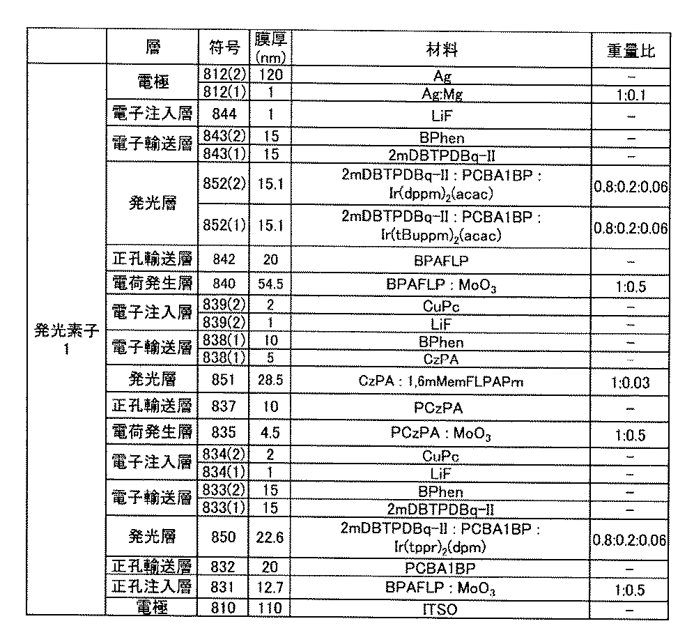
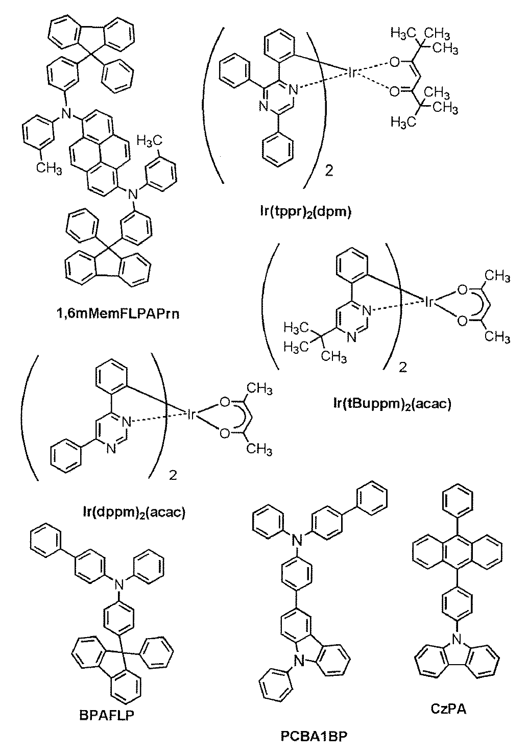

<発光素子の作製>
基板800上に電極810として、ITSO膜を厚さが110nmになるように形成した。なお、電極810の電極面積は、81cm2(9cm×9cm)とした。
基板800上に電極810として、ITSO膜を厚さが110nmになるように形成した。なお、電極810の電極面積は、81cm2(9cm×9cm)とした。
次に、電極810上に正孔注入層831として、BPAFLPと、酸化モリブデン(MoO3)と、を重量比(BPAFLP:MoO3)が1:0.5になるように、且つ、厚さが12.7nmになるように共蒸着した。
次に、正孔注入層831上に正孔輸送層832として、PCBA1BPを厚さが10nmになるように蒸着した。
次に、正孔輸送層832上に、発光層850として、2mDBTPDBq−IIと、PCBA1BPと、Ir(tppr)2(dpm)を重量比(2mDBTPDBq−II:PCBA1BP:Ir(tppr)2(dpm))が0.8:0.2:0.06になるように、且つ、厚さが22.6nmになるように共蒸着した。ここで、Ir(tppr)2(dpm)がゲスト材料であり、赤色の発光を示す。
次に、発光層850上に、電子輸送層833として、2mDBTPDBq−IIとBPhenとを、厚さがそれぞれ15nmとになるように順次蒸着した。
次に、電子輸送層833上に、電子注入層834として、フッ化リチウム(略称:LiF)と、銅フタロシアニン(略称:CuPc)とを、厚さがそれぞれ1nmと2nmとになるように順次蒸着した。
次に、正孔注入層を兼ねる電荷発生層835として、PCzPAと、酸化モリブデン(MoO3)と、を重量比(PCzPA:MoO3)が1:0.5になるように、且つ、厚さが4.5nmになるように共蒸着した。
次に、電荷発生層835上に正孔輸送層837として、PCzPAを厚さが10nmになるように蒸着した。
次に、正孔輸送層837上に、発光層851として、CzPAと1,6mMemFLPAPrnとを重量比(CzPA:1,6mMemFLPAPrn)が1:0.03となるように、且つ、厚さが28.5nmとなるように蒸着した。ここで、1,6mMemFLPAPrnがゲスト材料であり、青色の発光を示す。
次に、発光層851上に、電子輸送層838として、CzPAとBPhenとを、厚さがそれぞれ5nm、10nmとになるように順次蒸着した。
次に、電子輸送層838上に、電子注入層839として、フッ化リチウム(略称:LiF)と、銅フタロシアニン(略称:CuPc)とを、厚さがそれぞれ1nmと2nmとになるように順次蒸着した。
次に、正孔注入層を兼ねる電荷発生層840として、BPAFLPと、酸化モリブデン(MoO3)と、を重量比(BPAFLP:MoO3)が1:0.5になるように、且つ、厚さが54.5nmになるように共蒸着した。
次に、電荷発生層840上に正孔輸送層842として、BPAFLPを厚さが20nmになるように蒸着した。
次に、正孔輸送層842上に、発光層852として、2mDBTPDBq−IIと、PCBA1BPと、Ir(tBuppm)2(acac)を重量比(2mDBTPDBq−II:PCBA1BP:Ir(tBuppm)2(acac))が0.8:0.2:0.06になるように、且つ、厚さが15.1nmになるように共蒸着した。続いて、2mDBTPDBq−IIと、PCBAIBPと、Ir(dppm)2(acac)を重量比(2mDBTPDBq−II:PCBA1BP:Ir(dppm)2(acac))が0.8:0.2:0.06になるように、且つ、厚さが15.1nmになるように共蒸着した。ここで、Ir(tBuppm)2(acac)及びIr(dppm)2(acac))がゲスト材料であり、緑色、橙色の発光をそれぞれ示す。
次に、発光層852上に、電子輸送層843として、2mDBTPDBq−IIとBPhenとを、厚さがそれぞれ15nmとになるように順次蒸着した。
次に、電子輸送層843上に、電子注入層844として、フッ化リチウム(略称:LiF)を、厚さが1nmとになるように蒸着した。
次に、電子注入層844上に、電極812として、銀(Ag)とマグネシウム(Mg)と、を重量比(Ag:Mg)が1:0.1となるように、且つ厚さが1nmとなるように共蒸着した。続いて、Agを厚さが120nmとなるように蒸着した。
次に、窒素雰囲気のグローブボックス内において、有機EL用シール材を用いて封止するための基板802を、有機材料を形成した基板800に固定することで、発光素子1を封止した。具体的には、基板800に形成した有機材料の周囲にシール材を塗布し、該基板800と基板802とを貼り合わせ、波長が365nmの紫外光をシール材に6J/cm2照射し、80℃にて1時間熱処理した。以上の工程により発光素子1を得た。
<発光素子の分析>
次に、上記作製した発光素子1中の有機化合物の状態を分析するために、以下の工程(図3(S1)、(S4)、(S5)及び(S7)参照)により、発光素子1に含まれる有機化合物を単離、分取した。
次に、上記作製した発光素子1中の有機化合物の状態を分析するために、以下の工程(図3(S1)、(S4)、(S5)及び(S7)参照)により、発光素子1に含まれる有機化合物を単離、分取した。
まず、発光素子1の素子作製がなされていない対向基板にカッターで切っ掛けを入れ、一方の基板を剥離した(図3(S1))。
次に、EL層をクロロホルムを用いて溶かし出し、不要物をろ過することにより除去後、不要な溶媒を濃縮することで混合溶液を作製した(図3(S4))。
次に、混合溶液を液体クロマトグラフィーにより分離した(図3(S5))。分離はHPLCにより行った。装置は日本分析工業(株)社製リサイクル分取HPLC(LC−9130NEXT)を用いた。HPLC分析により得られたUV検出器(観測波長:254nm)のクロマトグラムを図19に示す。
図19に示すa乃至eの領域をそれぞれ異なる容器に分取した(図3(S7))。
続いて、図19において、最も大きなピークを有する領域cに含まれる有機化合物を詳細に分析するため、1H−NMR測定を行った。その結果を図20(a)に示す。また、発光素子1の作製に用いた、蒸着前の2mDBTPDBq−IIの1H−NMRスペクトルを図20(b)に合わせて示す。
図20(a)と図20(b)を比較すると、概ね同一のスペクトルを有していることが分かる。すなわち、図19中、領域cに含まれる有機化合物は2mDBTPDBq−IIであると同定される。また、図20(a)は蒸着後、図20(b)は蒸着前の2mDBTPDBq−IIの状態をそれぞれ表している。図20(a)と図20(b)にほとんど変化がないことから、2mDBTPDBq−IIは蒸着時の加熱や真空下において、分解や劣化を起こさない、耐圧性、耐熱性に優れた真空蒸着に好適に用いることができる有機化合物であることが分かった。
以上より、本発明の一態様に係る分析方法によって、発光素子に含まれる有機化合物を分析することができる。また、有機化合物の耐熱性や耐圧性を評価することができる。
本実施例では、本発明の一態様に係る分析方法の分析例について説明する。本実施例では、OLED素子が適用された、OLED素子構造が未知であり、画面面積が5.5インチであるA社製スマートフォンに使用されている発光素子の分析例について以下説明する。以下、A社製スマートフォンに使用されている発光素子を発光素子2と記載する。
<発光素子のGCIB−TOF−SIMS分析>
他の分析により、発光素子2は赤色(R)画素、緑色(G)画素、青色(B)画素を有することが分かった。そこで、各画素について、それぞれGCIB−TOF−SIMS分析を行った(図3(S1)乃至(S3))。
他の分析により、発光素子2は赤色(R)画素、緑色(G)画素、青色(B)画素を有することが分かった。そこで、各画素について、それぞれGCIB−TOF−SIMS分析を行った(図3(S1)乃至(S3))。
まず、実施例1と同様に、発光素子2が形成されていない基板を剥離した(図3(S1))。
次に、粘着性のテープを用いて露出している電極を剥離した(図3(S2))。
次に、R、G、B各画素について、それぞれAr−GCIBを用いてGCIB−TOF−SIMS分析を行った(S2)。その結果を表2乃至表4に示す。表2はR画素、表3はG画素、表4はB画素の分析結果をそれぞれ示す。表2乃至表4から発光素子2はR、B各画素は有機化合物を含む層が5層積層された構造を有し、G画素は6層積層されていることが分かった。表2乃至表4では質量電荷比が検出された順番に便宜上A層、B層乃至E層またはF層と記載している。


また、剥離した電極の有機層側の剥離表面についてGCIB−TOF−SIMS分析を行ったところ、有機化合物はほとんど検出されなかった。よって、S2の工程において電極のみが剥離され、有機化合物からなる層は基板側に残存していることが分かった。また、電極のToF−SIMS分析からはLi、Mg、Ag、Ybが検出された。
また、剥離していない電極にはITOが使用されていることが分かった。
また表2乃至表4から、R画素及びB画素のD層とE画素のF層には同一の有機化合物が、R画素及びB画素のD層とG画素のE層には同一の有機化合物が、R、G、B画素それぞれのA層に同一の有機化合物が用いられていることが推定できる。
また、R画素のB層において、m/z=769付近に検出されるスペクトルの同位体ピークを分析したところ、m/z=769付近が検出される有機化合物はIrを有することが分かった。R画素は赤色に発光する機能があるため、該有機化合物が赤色燐光材料であると推定される。よって、R画素においてB層が発光層であると予想される。同じくB層から検出されるm/z=613付近が検出される有機化合物はホスト材料であることが予想される。
R画素と同様に、G画素のB層において、m/z=782付近に検出されるスペクトルの同位体ピークを分析したところ、m/z=782付近が検出される有機化合物はIrを有することが分かった。G画素は緑色に発光する機能があるため、該有機化合物が緑色燐光材料であると推定される。よって、G画素においてB層が発光層であると予想される。同じくB層から検出されるm/z=612付近及びm/z=636付近が検出される有機化合物はホスト材料であることが予想される。
同一の層から複数の有機化合物が検出された場合、該層は発光層の可能性がある。発光素子2において各画素のA層は2種類の有機化合物のm/zが検出されている。しかし、上述の通り、R及びG画素においてB層が発光層であると予想される。また、A層は電極に接している層である。電極に発光層を隣接させると、消光やプラズモン吸収等発光素子特性に悪影響を及ぼすことが知られている。そのため、各層のA層は発光層ではないと予想される。そのため、B画素においても、2種類の有機化合物のm/zが検出されているB層が発光層であると予想される。
上述のように、各層に含まれる有機化合物の種類数や有する元素、各層の位置関係をGCIB−TOF−SIMS分析から得ることができる。
<発光素子に用いられている有機化合物の単離>
続いて、発光素子2に用いられている有機化合物を単離した(図3(S4)乃至(S7))。
続いて、発光素子2に用いられている有機化合物を単離した(図3(S4)乃至(S7))。
TOF−SIMS測定を行ったサンプルのEL層をクロロホルムを用いて溶かし出した。不要物をろ過することにより除去し、混合溶液を作製した(図3(S4))。本工程では、前述のGCIB−TOF−SIMS測定を行うことで、各有機化合物が含まれる層が特定されるので画素ごとではなく、R、G、B画素すべての画素に含まれる有機化合物を同時に溶かし出しても構わない。すなわちGCIB−TOF−SIMS測定を行うことで、本工程を容易に行うことができる。
調整した混合溶液をLC−MS装置に注入し、LC部にて混合溶液中の有機化合物の分離を行った。LC−MS装置のLC部サーモフィッシャーサイエンティフィック社製Ultimate3000を、MS部にはサーモフィッシャーサイエンティフィック社製Q Exactiveを用いた。LC分析により得られたUV検出器(観測波長:254nm)のクロマトグラムを図21に示す。図21(b)は図21(a)の拡大図である。図21より15種類のピークが観測された。
<m/z=613が検出される有機化合物の同定>
以下、表2に示すR画素B層から検出される、m/z=613付近が検出される有機化合物の構造を同定する方法について説明する。以下、該有機化合物を有機化合物613と記載する。
以下、表2に示すR画素B層から検出される、m/z=613付近が検出される有機化合物の構造を同定する方法について説明する。以下、該有機化合物を有機化合物613と記載する。
LC−MS分析(図3中(S6))の結果から図21に示す、ピーク4からm/z=613.2380が検出された。そこで、ピーク4に関して、HPLCにて荒分けを行い、LC−MSのフラクションコレクターを用いて分取(S7)し、有機化合物613を得た。図22に有機化合物613を分取後のm/z=613付近が含まれる溶液に関して測定したUV検出器(観測波長:254nm)のクロマトグラムを示す。図22より有機化合物613が純度良く単離できていることが分かる。
次に、有機化合物613の構造を分析するために、1H−NMR測定を行った。その結果を図23(a)乃至図25(a)に示す。図24(a)は図23(a)の7ppm乃至9ppmを拡大した図であり、図25(a)は図23(a)の1ppm乃至3ppmを拡大した図である
上述のLC−MS測定から得られたm/z=613.2380より組成式を求め、該組成式と図23(a)乃至図25(a)から有機化合物613の分子構造を推定した。CAS推定した有機化合物の構造を以下に示す。推定した有機化合物は以下に示す、9−フェニル−9’−(4−フェニル−2−キナゾリニル)−3,3’−ビ−9H−カルバゾール(略称:PCCzQz)である。

次に、PCCzQzを合成した(図4(S11))。合成経路及び合成方法は特許文献2を参照した。
合成したPCCzQzの1H−NMRスペクトルを測定した。その結果を図23(b)乃至図25(b)に示す。図24(b)は図23(b)の7ppm乃至9ppmを拡大した図であり、図25(b)は図23(b)の1ppm乃至3ppmを拡大した図である。
図23乃至図25より、有機化合物613の1H−NMRスペクトルとPCCzQzの1H−NMRスペクトルは概ね一致した。よって、有機化合物613はPCCzQzであると同定された。すなわち、発光素子2のR画素にはPCCzQzが含まれていることが分かった。
<R画素の発光機構の分析1>
以下、表2に示すR画素B層の発光機構の分析方法について説明する。上述の通り、R画素B層は発光層と推定でき、該層に含まれる有機化合物613がホスト材料、m/z=769付近が検出される有機化合物はIrを有する有機化合物であるため、ゲスト材料であると推定される。以下、m/z=769付近が検出される有機化合物を有機化合物769と記載する。
以下、表2に示すR画素B層の発光機構の分析方法について説明する。上述の通り、R画素B層は発光層と推定でき、該層に含まれる有機化合物613がホスト材料、m/z=769付近が検出される有機化合物はIrを有する有機化合物であるため、ゲスト材料であると推定される。以下、m/z=769付近が検出される有機化合物を有機化合物769と記載する。
有機化合物613を分取した際と同様に、LC−MS分析(図3中(S6))の結果から図21に示す、ピーク15からm/z=769.31が検出された。そこで、ピーク15の部分の分離条件を再検討することで分離した。分離後、UV検出器(観測波長:254nm)のクロマトグラム中、有機化合物769が含まれるリテンションタイムにおける吸収スペクトルを、サーモフィッシャーサイエンティフィック社製Ultimate3000により測定した(図3中(S6))。測定した吸収スペクトルはアセトニトリル:水=95:5の混合溶液中における吸収スペクトルである。その結果を図26に示す。
次に、有機化合物613の発光スペクトル測定を行った。固体薄膜は石英基板上に真空蒸着法にて成膜することで作製した。発光スペクトルの測定には蛍光光度計((株)浜松ホトニクス製 FS920)を用いた。その結果を図27に示す。
図28に図26に示す吸収スペクトルと図27に示す発光スペクトルを重ね合わせたグラフを示す。図28より、ゲスト材料であると予想される有機化合物769の最も長波長側の吸収帯(MLCT吸収と予想される)と有機化合物613の発光スペクトルが重なっていることが分かる。よって、発光素子2のR画素中では、有機化合物613が有するエネルギーが有機化合物769にエネルギー移動することで、有機化合物769が発光を呈することが示唆された。
<R画素の発光機構の分析2>
以下に、上述とは異なる、表2に示すR画素の有機化合物の分析について説明する。上述の通り、R画素において発光層と推定されるB層と、隣接するC層の関係に関して分析を行った。
まず、表2に示すR画素C層から検出される、m/z=638付近が検出される有機化合物を単離、分取した。以下、m/z=638付近が検出される有機化合物を有機化合物638と記載する。
有機化合物613を分取した際と同様に、LC−MS分析(図3中(S6))の結果から図21に示す、ピーク7からm/z=638付近にピークが検出されたため、ピーク7の部分を分取することにより、有機化合物638を得た。
次に、有機化合物638の薄膜における発光スペクトル測定を行った。固体薄膜は石英基板上に真空蒸着法にて成膜することで作製した。薄膜の吸収スペクトルの測定には、分光光度計((株)日立ハイテクノロジーズ製 分光光度計U4100)を用いた。
図29に、測定した有機化合物638の吸収スペクトルと図27に示す有機化合物613の発光スペクトルを重ね合わせたグラフを示す。図29より有機化合物638の吸収スペクトルと有機化合物613の発光スペクトルは重なりを有さないことが分かる。すなわち、有機化合物613のエネルギーが有機化合物638へはエネルギー移動しにくいことが分かる。これにより、C層は発光層と推定されるB層の励起子ブロック層としての機能を有していることが示唆される。
<有機化合物613の発光寿命測定>
R画素B層から検出された有機化合物613の発光寿命測定を行った。測定にはピコ秒蛍光寿命測定システム(浜松ホトニクス社製)を用いた。測定には有機化合物613の薄膜を用い、石英基板上に真空蒸着により厚さ30nmとなるように成膜し作製した。なお、薄膜の作製には発光素子2から分取した有機化合物613を用いた。本測定では、薄膜が呈する蛍光発光の寿命を測定するため、薄膜にパルスレーザーを照射し、レーザー照射後から減衰していく発光をストリークカメラにより時間分解測定した。パルスレーザーには波長が337nmの窒素ガスレーザを用い、500psのパルスレーザーを10Hzの周期で薄膜に照射し、繰り返し測定したデータを積算することにより、S/N比の高いデータを得た。また、測定は室温(23℃に保たれた雰囲気)で行った。
R画素B層から検出された有機化合物613の発光寿命測定を行った。測定にはピコ秒蛍光寿命測定システム(浜松ホトニクス社製)を用いた。測定には有機化合物613の薄膜を用い、石英基板上に真空蒸着により厚さ30nmとなるように成膜し作製した。なお、薄膜の作製には発光素子2から分取した有機化合物613を用いた。本測定では、薄膜が呈する蛍光発光の寿命を測定するため、薄膜にパルスレーザーを照射し、レーザー照射後から減衰していく発光をストリークカメラにより時間分解測定した。パルスレーザーには波長が337nmの窒素ガスレーザを用い、500psのパルスレーザーを10Hzの周期で薄膜に照射し、繰り返し測定したデータを積算することにより、S/N比の高いデータを得た。また、測定は室温(23℃に保たれた雰囲気)で行った。
上記測定結果を図30に示す。図30に示すように、発光素子2から分取した有機化合物を用いて、ノイズが少ない発光寿命特性を測定できたことが分かる。
<有機化合物613の三重項励起(T1)準位の測定>
R画素B層から検出された有機化合物613の燐光スペクトルを測定し、T1準位を求めた。測定には、上述の発光寿命測定に用いた薄膜を用い、顕微PL装置 LabRAM HR−PL((株)堀場製作所)を用い、測定温度は10K、励起光としてHe−Cdレーザー(325nm)を用い、検出器にはCCD検出器を用いた。
R画素B層から検出された有機化合物613の燐光スペクトルを測定し、T1準位を求めた。測定には、上述の発光寿命測定に用いた薄膜を用い、顕微PL装置 LabRAM HR−PL((株)堀場製作所)を用い、測定温度は10K、励起光としてHe−Cdレーザー(325nm)を用い、検出器にはCCD検出器を用いた。
上記測定結果を図31に示す。図31に示すように、発光素子2から分取した有機化合物を用いて、ノイズが少ない燐光スペクトルを測定できたことが分かる。また、図31より、この燐光の短波長側の第一ピークは536nmであり、これより有機化合物613のT1準位は2.31eVであると算出された。
<G画素の発光機構の分析>
以下、表3に示すG画素B層の発光機構の分析方法について説明する。上述の通り、G画素B層に含まれるm/z=782が検出される有機化合物はIrを有する有機化合物であり、ゲスト材料であると推定され、m/z=612、636が検出される有機化合物はホスト材料であると推定される。以下、m/z=782、612、636が検出される有機化合物をそれぞれ有機化合物782、有機化合物612、有機化合物636と記載する。
以下、表3に示すG画素B層の発光機構の分析方法について説明する。上述の通り、G画素B層に含まれるm/z=782が検出される有機化合物はIrを有する有機化合物であり、ゲスト材料であると推定され、m/z=612、636が検出される有機化合物はホスト材料であると推定される。以下、m/z=782、612、636が検出される有機化合物をそれぞれ有機化合物782、有機化合物612、有機化合物636と記載する。
図21に示す、ピーク1からm/z=783.30が、ピーク6からm/z=612.24が、ピーク8からm/z=636.25がそれぞれ検出された。そこで、有機化合物613単離時と同様に、各ピーク付近に関してHPLCで荒分けを行い、LC−MSのフラクションコレクターにて分取(S7)し、有機化合物782、有機化合物612、有機化合物636を得た。なお、有機化合物782に対応する質量電荷比はm/z=783.30とTOF−SIMS測定時の値より1大きい値となるが、これはLC−MS測定時のプロトンが付加することでイオン化したと考えられるため、表3中m/z=782として検出された有機化合物とLC−MS測定時にm/z=783.30として検出されたイオンに由来する有機化合物は同一である。
単離した有機化合物782のトルエン溶液による吸収スペクトルを測定した。その結果を図32に示す。トルエン溶液の吸収スペクトルの測定には、紫外可視分光光度計((株)日本分光製 V550型)を用い、トルエンのみを石英セルに入れて測定したスペクトルを差し引いた。
次に、有機化合物612及び有機化合物636の薄膜の発光スペクトルを測定した。薄膜は有機化合物のトルエン溶液を基板に滴下し、溶媒を蒸発させることで作製した。発光スペクトルの測定には上述の蛍光光度計を用いた。その結果を図33に示す。
また、有機化合物612と有機化合物636の混合膜を作製し、発光スペクトルを測定した。該混合膜は有機化合物612のトルエン溶液と有機化合物636のトルエン溶液を混合し、同一基板に滴下し、溶媒を蒸発させることで作製した。発光スペクトルの測定には上述の蛍光光度計を用いた。その結果を図33に合わせて示す。
ここで、図33から有機化合物612と有機化合物636の混合膜の発光スペクトルは、個々の有機化合物の発光スペクトルよりも長波長側にピークを有することが分かる。すなわち、有機化合物612と有機化合物636の混合膜はエキサイプレックスを形成していることが分かる。
次に、有機化合物782のトルエン溶液における吸収スペクトルと有機化合物612及び有機化合物636の混合膜の発光スペクトルの重なりを分析した。その結果を図34に示す。図34より有機化合物612と有機化合物636の混合膜の発光、すなわち、有機化合物612及び有機化合物636からなる励起錯体の発光は、ゲスト材料であると予想される有機化合物782の最も長波長側の吸収帯(MLCT吸収と予想される)と重なっていることが分かる。よって、発光素子2のG画素中では、有機化合物612及び有機化合物636からなる励起錯体が有するエネルギーが有機化合物782にエネルギー移動することで、有機化合物782が発光を呈することが示唆された。換言すると、発光素子2のG画素中では、ExTETが生じていることが示唆された。
上述の通り、本発明の分析方法を用いることで、発光素子中の有機化合物を分析することができる。また、発光素子中の有機化合物を用いて、該有機化合物の分子構造や様々な物性が測定できることが分かった。
本実施例では、本発明の一態様に係る分析方法の分析例について説明する。本実施例では、OLED素子が適用された、OLED素子構造が未知であり、A社製スマートフォンに使用されている発光素子の分析例について以下説明する。以下、本実施例で使用した発光素子を発光素子3と記載する。
まず、実施例1及び実施例2と同様に、発光素子3が形成されていない基板を剥離した(図3(S1))。この時、剥離した基板とともに一方の電極も剥離された。すなわち、剥離した基板に一方の電極が付着していた。
次に、粘着性のテープを用いて上記基板に付着した電極を剥離し、電極の基板側を露出させた。
<発光素子のTOF−SIMS分析>
次に、電極の基板側に関して、TOF−SIMS分析を行った(図36(S26))。その結果、m/z=483、661、803及び818にピークが観測された。
次に、電極の基板側に関して、TOF−SIMS分析を行った(図36(S26))。その結果、m/z=483、661、803及び818にピークが観測された。
<電極の基板側の有機層に用いられている有機化合物の単離>
続いて、発光素子2に用いられている有機化合物を単離した(図36(S4)乃至(S7))。
続いて、発光素子2に用いられている有機化合物を単離した(図36(S4)乃至(S7))。
剥離した電極のサンプルを重クロロホルムを用いて溶かし出した。その後、不要物をろ過することにより除去し、混合溶液を作製した(図36(S4))。
調整した混合溶液をLC−MS装置に注入し、LC部にて混合溶液中の有機化合物の分離を行った。LC分析により得られたUV検出器(観測波長:254nm)のクロマトグラムを図37に示す。
<m/z=818が検出される有機化合物の同定>
m/z=818付近が検出される有機化合物の構造を同定する方法について説明する。以下、該有機化合物を有機化合物818と記載する。
m/z=818付近が検出される有機化合物の構造を同定する方法について説明する。以下、該有機化合物を有機化合物818と記載する。
図37にピークIからm/z=819.34が検出された。そこで、ピークIに関して、LC−MSのフラクションコレクターを用いて分取(図36(S7))し、有機化合物818を得た。
次に、有機化合物818の構造を分析するために、1H−NMR測定を行った。その結果を図38(a)及び図39(a)に示す。図39(a)は図38(a)の6.5ppm乃至9。0ppmを拡大した図である。
上述のLC−MS測定から得られたm/z=819.34及び図38(a)及び39(a)から有機化合物818の分子構造を推定した。推定した有機化合物は以下に示す、N,N’−ジフェニル−N,N’−ビス(9−フェニル−9−H−カルバゾール−3−イル)−(1,1’−ビフェニル)−4,4’−ジアミン(略称:BPPCA)である。

次に、実際にBPPCAを合成した(図4(S11))。
合成したBPPCAの1H−NMRスペクトルを測定した。その結果を図38(b)乃及び図39(b)に示す。図39(b)は図38(b)の6.5ppm乃至9。0ppmを拡大した図である。
図39乃至図39より、有機化合物818の1H−NMRスペクトルとBPPCAの1H−NMRスペクトルは概ね一致した。よって有機化合物818はBPPCAであると同定された。すなわち、発光素子3の電極の基板側にはBPPCAが含まれていることが分かった。
20 有機半導体層、50 有機半導体素子、100 EL層、101 電極、101a 導電層、101b 導電層、101c 導電層、102 電極、103 電極、103a 導電層、103b 導電層、104 電極、104a 導電層、104b 導電層、106 発光ユニット、110 発光ユニット、111 正孔注入層、112 正孔輸送層、113 電子輸送層、114 電子注入層、115 電荷発生層、116 正孔注入層、117 正孔輸送層、118 電子輸送層、119 電子注入層、120 発光層、121 ホスト材料、121_1 有機化合物、121_2 有機化合物、122 発光性材料、123B 発光層、123G 発光層、123R 発光層、130 発光層、131 発光性材料、132 有機化合物、145 隔壁、150 発光素子、170 発光層、190 発光層、200 基板、210 基板、220 基板、221B 領域、221G 領域、221R 領域、222B 領域、222G 領域、222R 領域、223 遮光層、224B 光学素子、224G 光学素子、224R 光学素子、250 発光素子、252 発光素子、260a 発光素子、260b 発光素子、262a 発光素子、262b 発光素子、400 基板、410 基板、420 キャップ膜、601 ソース側駆動回路、602 画素部、603 ゲート側駆動回路、604 封止基板、605 シール材、607 空間、608 配線、610 素子基板、611 スイッチング用TFT、612 電流制御用TFT、613 電極、614 絶縁物、616 EL層、617 電極、618 発光素子、623 nチャネル型TFT、624 pチャネル型TFT、800 基板、802 基板、810 電極、812 電極、831 正孔注入層、832 正孔輸送層、833 電子輸送層、834 電子注入層、835 電荷発生層、837 正孔輸送層、838 電子輸送層、839 電子注入層、840 電荷発生層、842 正孔輸送層、843 電子輸送層、844 電子注入層、850 発光層、851 発光層、852 発光層、900 携帯情報端末、901 筐体、902 筐体、903 表示部、905 ヒンジ部、910 携帯情報端末、911 筐体、912 表示部、913 操作ボタン、914 外部接続ポート、915 スピーカ、916 マイク、917 カメラ、920 カメラ、921 筐体、922 表示部、923 操作ボタン、924 シャッターボタン、926 レンズ、1001 基板、1002 下地絶縁膜、1003 ゲート絶縁膜、1006 ゲート電極、1007 ゲート電極、1008 ゲート電極、1020 層間絶縁膜、1021 層間絶縁膜、1022 電極、1024B 電極、1024G 電極、1024R 電極、1024W 電極、1025B 下部電極、1025G 下部電極、1025R 下部電極、1025W 下部電極、1026 隔壁、1028 EL層、1029 電極、1031 封止基板、1032 シール材、1033 基材、1034B 着色層、1034G 着色層、1034R 着色層、1036 オーバーコート層、1037 層間絶縁膜、1040 画素部、1041 駆動回路部、1042 周辺部、3054 表示部、3500 多機能端末、3502 筐体、3504 表示部、3506 カメラ、3508 照明、3600 ライト、3602 筐体、3608 照明、3610 スピーカ、8501 照明装置、8502 照明装置、8503 照明装置、8504 照明装置、9000 筐体、9001 表示部、9003 スピーカ、9005 操作キー、9006 接続端子、9007 センサ、9008 マイクロフォン、9055 ヒンジ、9200 携帯情報端末、9201 携帯情報端末、9202 携帯情報端末
Claims (24)
- 一対の電極間に一つまたは複数の層を含む有機半導体層を有する有機半導体素子の分析方法であって、
前記有機半導体素子の一方の電極を剥離する工程と、
露出した前記有機半導体層の層構造および/または混合状態を、第1の質量分析法により分析する工程と、
前記有機半導体層の各層に含まれる有機化合物のうち、いずれか一または複数を溶剤により溶出させ、溶液を作製する工程と、
液体クロマトグラフィーを用いて、前記溶液に含まれる有機化合物を単離し、当該単離した有機化合物を第2の質量分析法により分析する工程と、
前記第1の質量分析法により検出した質量電荷比と、前記第2の質量分析法により検出した質量電荷比とを対比する工程と、
前記単離した有機化合物の物性を測定する工程と、を有する有機半導体素子の分析方法。 - 請求項1において、
前記物性はNMRスペクトル、吸収スペクトル、発光スペクトル、発光寿命の少なくともいずれか一である有機半導体素子の分析方法。 - 請求項1または2において、
前記第2の質量分析法では、少なくとも第1の有機化合物が検出され、
前記第1の有機化合物の質量電荷比から組成式を推定する工程と、
前記第1の有機化合物のNMR測定により、前記第1の有機化合物の第1のNMRスペクトルを取得する工程と、
前記組成式と前記NMRスペクトルと、を用いて第2の有機化合物を推定する工程と、
前記第2の有機化合物を合成する工程と、
前記NMR測定により、前記第2の有機化合物の第2のNMRスペクトルを取得する工程と、
前記第1のNMRスペクトルと、前記第2のNMRスペクトルと、を対比する工程を有する、有機半導体素子の分析方法。 - 請求項1または2において、
前記溶液の1H−NMRを測定する工程と、
少なくとも二つの有機化合物を単離する工程と、
前記少なくとも二つの有機化合物の各1H−NMRを測定する工程と、
前記溶液の1H−NMRと前記少なくとも二つの有機化合物の各1H−NMRとを対比することにより、前記少なくとも二つの有機化合物のモル比を算出する工程を含む、有機半導体素子の分析方法。 - 一対の電極間に一つまたは複数の層を含む有機半導体層を有する有機半導体素子の分析方法であって、
前記有機半導体素子の一方の電極を剥離する工程と、
露出した前記有機半導体層の層構造および/または混合状態を、第1の質量分析法により分析する工程と、
前記第1の質量分析法から複数の有機化合物を含む第1の層を特定する工程と、
前記有機半導体層の各層に含まれる有機化合物のうち、いずれか一または複数を溶剤により溶出させ、溶液を作製する工程と、
液体クロマトグラフィーを用いて、前記溶液に含まれる有機化合物を単離し、単離した有機化合物を第2の質量分析法により分析する工程と、
前記第1の質量分析法により検出した質量電荷比と、前記第2の質量分析法により検出した質量電荷比とを対比する工程と、
前記有機半導体層の前記第1の層に含まれる第1の有機化合物と第2の有機化合物とを単離した化合物の中から決定する工程と、前記第1の有機化合物の第1の発光スペクトルを測定する工程と、
前記第2の有機化合物の第2の発光スペクトルを測定する工程と、
前記第1の有機化合物及び前記第2の有機化合物の混合物の第3の発光スペクトルを測定する工程と、を有する、有機半導体素子の分析方法。 - 一対の電極間に一つまたは複数の層を含む有機半導体層を有する有機半導体素子の分析方法であって、
前記有機半導体素子の一方の電極を剥離する工程と、
露出した前記有機半導体層の層構造および/または混合状態を、第1の質量分析法により分析し複数の有機化合物を含む第1の層を特定する工程と、
前記有機半導体層の各層に含まれる有機化合物のうち、いずれか一または複数を溶剤により溶出させ、溶液を作製する工程と、
液体クロマトグラフィーを用いて、前記溶液に含まれる有機化合物を単離し、単離した有機化合物を第2の質量分析法により分析する工程と、
前記第1の質量分析法により検出した質量電荷比と、前記第2の質量分析法により検出した質量電荷比とを対比し、前記有機半導体層の前記第1の層に含まれる第1の有機化合物と第2の有機化合物とを推定する工程と、
前記第1の有機化合物の発光寿命を測定する工程と、
前記第1の有機化合物の吸収スペクトルを測定する工程と、
前記第2の有機化合物の発光スペクトルを測定する工程と、を有する、有機半導体素子の分析方法。 - 一対の電極間に一つまたは複数の層を含む有機半導体層を有する有機半導体素子の分析方法であって、
前記有機半導体素子の一方の電極を剥離する工程と、
露出した前記有機半導体層の層構造および/または混合状態を、第1の質量分析法により分析し複数の有機化合物を含む第1の層を特定する工程と、
前記有機半導体層の各層に含まれる有機化合物のうち、いずれか一または複数を溶剤により溶出させ、溶液を作製する工程と、
液体クロマトグラフィーを用いて、前記溶液に含まれる有機化合物を単離し、単離した有機化合物を第2の質量分析法により分析する工程と、
前記第1の質量分析法により検出した質量電荷比と、前記第2の質量分析法により検出した質量電荷比とを対比し、前記有機半導体層の前記第1の層に含まれる第1の有機化合物、第2の有機化合物及び第3の有機化合物を推定する工程と、
前記第1の有機化合物の発光寿命を測定する工程と
前記第2の有機化合物の吸収スペクトルを測定する工程と、
前記第2の有機化合物の第1の発光スペクトルを測定する工程と、
前記第3の有機化合物の第2の発光スペクトルを測定する工程と、
前記第2の有機化合物及び前記第3の有機化合物の混合物の第3の発光スペクトルを測定する工程と、を有する、有機半導体素子の分析方法。 - 一対の電極間に一つまたは複数の層を含む有機半導体層を有する有機半導体素子の分析方法であって、
前記有機半導体層はIrを有する第1の有機化合物を有し、
前記有機半導体素子の一方の電極を剥離する工程と、
露出した前記有機半導体層の層構造および/または混合状態を、第1の質量分析法により分析し複数の有機化合物を含む第1の層を特定する工程と、
前記有機半導体層の各層に含まれる有機化合物のいずれか一または複数を溶剤により溶出させ、溶液を作製する工程と、
液体クロマトグラフィーを用いて、前記溶液に含まれる有機化合物を単離し、単離した有機化合物を第2の質量分析法により分析する工程と、
前記第1の質量分析法により検出した質量電荷比と、前記第2の質量分析法により検出した質量電荷比とを対比し、前記有機半導体層の前記第1の層に含まれるに含まれる第1の有機化合物と第2の有機化合物とを推定する工程と、
前記第1の有機化合物の吸収スペクトルを測定する工程と、
前記第2の有機化合物の発光スペクトルを測定する工程と、を有する、有機半導体素子の分析方法。 - 一対の電極間に一つまたは複数の層を含む有機半導体層を有する有機半導体素子の分析方法であって、
前記有機半導体層はIrを有する第1の有機化合物を有し、
前記有機半導体素子の一方の電極を剥離する工程と、
露出した前記有機半導体層の層構造および/または混合状態を、第1の質量分析法により分析し複数の有機化合物を含む第1の層を特定する工程と、
前記有機半導体層の各層に含まれる有機化合物のいずれか一または複数を溶剤により溶出させ、溶液を作製する工程と、
液体クロマトグラフィーを用いて、前記溶液に含まれる有機化合物を単離し、単離した有機化合物を第2の質量分析法により分析する工程と、
前記第1の質量分析法により検出した質量電荷比と、前記第2の質量分析法により検出した質量電荷比とを対比し、前記有機半導体層の前記第1の層に含まれる第1の有機化合物、第2の有機化合物及び第3の有機化合物を推定する工程と、
前記第1の有機化合物の吸収スペクトルを測定する工程と、
前記第2の有機化合物の第1の発光スペクトルを測定する工程と、
前記第3の有機化合物の第2の発光スペクトルを測定する工程と、
前記第2有機化合物及び前記第3の有機化合物の混合物の第3の発光スペクトルを測定する工程と、を有する、有機半導体素子の分析方法。 - 請求項1または2において、
前記有機半導体素子はEL素子である、有機半導体素子の分析方法。 - 請求項1または2において、
前記有機半導体素子は光電変換素子である、有機半導体素子の分析方法。 - 請求項1または2において、
前記有機半導体層が単一の有機化合物からなる、有機半導体素子の分析方法。 - 請求項1または2において、
前記有機半導体層が正孔輸送材料を含む第1の層と、発光物質を含む第2の層と、電子輸送材料を含む第3の層を有し、
前記陽極側から第1の層、第2の層、第3の層の順で積層され、第1の層と第2の層は接しており、第2の層と第3の層は接している、有機半導体素子の分析方法。 - 請求項13において、
前記発光物質として燐光発光化合物を含む有機半導体素子の分析方法。 - 請求項13において、
前記第2の層に燐光発光物質と、第1の化合物と第2の化合物を含み、第1の化合物と第2の化合物は励起錯体を形成する有機半導体素子の分析方法。 - 請求項13において、
前記第2の層が熱活性型遅延蛍光を示す材料を有する有機半導体素子の分析方法。 - 請求項1または2において、
前記第1の質量分析がGCIB−TOF−SIMS分析、斜め切削後のTOF−SIMS、または斜め切削後のMALDI−TOF−MSのいずれか一である有機半導体素子の分析方法。 - 請求項1または2において、
前記第2の質量分析がLC−MS分析である有機半導体素子の分析方法。 - 請求項1または2において、
前記第2の質量分析において、検出される質量電荷比を小数点第3位以下まで測定する、有機半導体素子の分析方法。 - 請求項1または2において、
前記有機半導体層の膜厚が100nm以上1μm以下である、有機半導体素子の分析方法。 - 請求項1または2において、
前記有機半導体素子を、4mm2以上100cm2以下の面積に加工する工程を有する、有機半導体素子の分析方法。 - 請求項1または2において、
前記有機半導体素子の面積が4mm2以上100cm2以下である、有機半導体素子の分析方法。 - 請求項1または2において、
前記有機半導体層の単位面積当たりの重量が1μg/cm2以上100μg/cm2以下である、有機半導体素子の分析方法。 - 請求項1または2において、
前記有機半導体層の重量が0.04μg以上1mg以下である、有機半導体素子の分析方法。
Priority Applications (3)
| Application Number | Priority Date | Filing Date | Title |
|---|---|---|---|
| CN201880017551.5A CN110402387B (zh) | 2017-04-04 | 2018-03-26 | 有机半导体元件的分析方法 |
| US16/498,141 US11088328B2 (en) | 2017-04-04 | 2018-03-26 | Method of analyzing organic semiconductor element |
| JP2019510495A JP7185620B2 (ja) | 2017-04-04 | 2018-03-26 | 有機半導体素子の分析方法 |
Applications Claiming Priority (2)
| Application Number | Priority Date | Filing Date | Title |
|---|---|---|---|
| JP2017-074690 | 2017-04-04 | ||
| JP2017074690 | 2017-04-04 |
Publications (1)
| Publication Number | Publication Date |
|---|---|
| WO2018185599A1 true WO2018185599A1 (ja) | 2018-10-11 |
Family
ID=63713355
Family Applications (1)
| Application Number | Title | Priority Date | Filing Date |
|---|---|---|---|
| PCT/IB2018/052022 Ceased WO2018185599A1 (ja) | 2017-04-04 | 2018-03-26 | 有機半導体素子の分析方法 |
Country Status (4)
| Country | Link |
|---|---|
| US (1) | US11088328B2 (ja) |
| JP (1) | JP7185620B2 (ja) |
| CN (1) | CN110402387B (ja) |
| WO (1) | WO2018185599A1 (ja) |
Cited By (1)
| Publication number | Priority date | Publication date | Assignee | Title |
|---|---|---|---|---|
| JP2022518570A (ja) * | 2019-01-29 | 2022-03-15 | コリア リサーチ インスティチュート オブ スタンダーズ アンド サイエンス | Ldi-msを用いた血液中の有機物の測定方法およびそのための装置 |
Families Citing this family (4)
| Publication number | Priority date | Publication date | Assignee | Title |
|---|---|---|---|---|
| EP4191236A1 (en) * | 2017-05-23 | 2023-06-07 | Hamamatsu Photonics K.K. | Orientation characteristic measurement method, orientation characteristic measurement program, and orientation characteristic measurement device |
| CN114284163B (zh) * | 2020-09-28 | 2025-01-17 | 长鑫存储技术有限公司 | 晶圆样品分析方法和装置 |
| KR102814300B1 (ko) * | 2020-12-04 | 2025-05-28 | 주식회사 엘지화학 | 유기 발광 소자의 유기물층용 물질의 광안정성 평가장치 및 평가방법 |
| US20250319990A1 (en) * | 2024-01-05 | 2025-10-16 | Hughey & Phillips, Llc | Light Emitting Diode Precision Approach Path Indicator |
Citations (7)
| Publication number | Priority date | Publication date | Assignee | Title |
|---|---|---|---|---|
| JP2007324233A (ja) * | 2006-05-30 | 2007-12-13 | Canon Inc | 有機エレクトロルミネッセンス素子およびその製造方法 |
| JP2012215554A (ja) * | 2011-03-31 | 2012-11-08 | Sumitomo Chemical Co Ltd | 液体クロマトグラフ−核磁気共鳴分析システム |
| JP2013024570A (ja) * | 2011-07-15 | 2013-02-04 | Semiconductor Energy Lab Co Ltd | 燐光測定方法 |
| JP2013242302A (ja) * | 2012-04-24 | 2013-12-05 | Semiconductor Energy Lab Co Ltd | 分析装置及び分析方法 |
| JP2014078699A (ja) * | 2012-09-21 | 2014-05-01 | Semiconductor Energy Lab Co Ltd | 発光素子 |
| JP2015165491A (ja) * | 2014-02-06 | 2015-09-17 | 三菱化学株式会社 | 有機電界発光素子及びその製造方法 |
| JP2016086171A (ja) * | 2014-10-28 | 2016-05-19 | 株式会社半導体エネルギー研究所 | 発光素子、発光装置、電子機器、及び照明装置 |
Family Cites Families (11)
| Publication number | Priority date | Publication date | Assignee | Title |
|---|---|---|---|---|
| GB1465692A (en) | 1973-05-10 | 1977-02-23 | Shell Int Research | Preparation of derivatives of cyclobutane and/or cyclobutene |
| JP2580988B2 (ja) * | 1993-12-17 | 1997-02-12 | 日本電気株式会社 | 有機物分析装置および有機物分析方法 |
| TW430996B (en) * | 1999-10-05 | 2001-04-21 | Ind Tech Res Inst | Structure and manufacturing method of a thin-film transistor with multiple gate structure |
| US20060166370A1 (en) * | 2002-03-08 | 2006-07-27 | Bailey Thomas H | Managing semiconductor process solutions using in-process mass spectrometry |
| KR100725460B1 (ko) * | 2005-12-28 | 2007-06-07 | 삼성전자주식회사 | 금속 오염 분석용 표준 시료의 제조 방법 |
| JP2009059935A (ja) * | 2007-08-31 | 2009-03-19 | Tosoh Corp | 有機半導体素子およびその製造方法 |
| KR101427611B1 (ko) | 2011-03-08 | 2014-08-11 | 롬엔드하스전자재료코리아유한회사 | 신규한 유기 전자재료용 화합물 및 이를 포함하는 유기 전계 발광 소자 |
| KR20140021014A (ko) * | 2011-05-11 | 2014-02-19 | 바스프 에스이 | 할로겐화 페릴렌계 반도체 물질 |
| US9355826B2 (en) * | 2012-02-17 | 2016-05-31 | A School Corporation Kansai University | Method for imaging mass analysis using physical vapor deposition of platinum nanoparticles |
| JP2015087237A (ja) * | 2013-10-30 | 2015-05-07 | キヤノン株式会社 | 質量分布計測方法及び質量分布計測装置 |
| JP6365770B2 (ja) * | 2015-04-24 | 2018-08-01 | 株式会社島津製作所 | 光学分析装置及びその製造方法 |
-
2018
- 2018-03-26 US US16/498,141 patent/US11088328B2/en active Active
- 2018-03-26 CN CN201880017551.5A patent/CN110402387B/zh active Active
- 2018-03-26 WO PCT/IB2018/052022 patent/WO2018185599A1/ja not_active Ceased
- 2018-03-26 JP JP2019510495A patent/JP7185620B2/ja active Active
Patent Citations (7)
| Publication number | Priority date | Publication date | Assignee | Title |
|---|---|---|---|---|
| JP2007324233A (ja) * | 2006-05-30 | 2007-12-13 | Canon Inc | 有機エレクトロルミネッセンス素子およびその製造方法 |
| JP2012215554A (ja) * | 2011-03-31 | 2012-11-08 | Sumitomo Chemical Co Ltd | 液体クロマトグラフ−核磁気共鳴分析システム |
| JP2013024570A (ja) * | 2011-07-15 | 2013-02-04 | Semiconductor Energy Lab Co Ltd | 燐光測定方法 |
| JP2013242302A (ja) * | 2012-04-24 | 2013-12-05 | Semiconductor Energy Lab Co Ltd | 分析装置及び分析方法 |
| JP2014078699A (ja) * | 2012-09-21 | 2014-05-01 | Semiconductor Energy Lab Co Ltd | 発光素子 |
| JP2015165491A (ja) * | 2014-02-06 | 2015-09-17 | 三菱化学株式会社 | 有機電界発光素子及びその製造方法 |
| JP2016086171A (ja) * | 2014-10-28 | 2016-05-19 | 株式会社半導体エネルギー研究所 | 発光素子、発光装置、電子機器、及び照明装置 |
Cited By (2)
| Publication number | Priority date | Publication date | Assignee | Title |
|---|---|---|---|---|
| JP2022518570A (ja) * | 2019-01-29 | 2022-03-15 | コリア リサーチ インスティチュート オブ スタンダーズ アンド サイエンス | Ldi-msを用いた血液中の有機物の測定方法およびそのための装置 |
| JP7126623B2 (ja) | 2019-01-29 | 2022-08-26 | コリア リサーチ インスティチュート オブ スタンダーズ アンド サイエンス | Ldi-msを用いた血液中の有機物の測定方法およびそのための装置 |
Also Published As
| Publication number | Publication date |
|---|---|
| CN110402387A (zh) | 2019-11-01 |
| JPWO2018185599A1 (ja) | 2020-03-19 |
| US11088328B2 (en) | 2021-08-10 |
| CN110402387B (zh) | 2022-07-15 |
| US20210119126A1 (en) | 2021-04-22 |
| JP7185620B2 (ja) | 2022-12-07 |
Similar Documents
| Publication | Publication Date | Title |
|---|---|---|
| JP7813938B2 (ja) | 発光デバイス | |
| JP7717139B2 (ja) | 発光素子、発光装置、電子機器および照明装置 | |
| JP2022189942A (ja) | 発光装置 | |
| JP7353440B2 (ja) | 化合物 | |
| US20210151689A1 (en) | Organic Compound, Light-Emitting Element, Light-Emitting Device, Electronic Device, and Lighting Device | |
| JP2022082817A (ja) | 発光装置 | |
| US10868258B2 (en) | Organic compound, light-emitting element, light-emitting device, electronic device, and lighting device | |
| JP7185620B2 (ja) | 有機半導体素子の分析方法 | |
| JP7490833B2 (ja) | 有機化合物および発光素子 | |
| WO2020229918A1 (ja) | 発光デバイス、発光機器、表示装置、電子機器及び照明装置 | |
| JP2025081446A (ja) | 有機化合物 | |
| WO2018154408A1 (ja) | 発光素子、発光装置、電子機器、および照明装置 |
Legal Events
| Date | Code | Title | Description |
|---|---|---|---|
| 121 | Ep: the epo has been informed by wipo that ep was designated in this application |
Ref document number: 18781683 Country of ref document: EP Kind code of ref document: A1 |
|
| ENP | Entry into the national phase |
Ref document number: 2019510495 Country of ref document: JP Kind code of ref document: A |
|
| NENP | Non-entry into the national phase |
Ref country code: DE |
|
| 122 | Ep: pct application non-entry in european phase |
Ref document number: 18781683 Country of ref document: EP Kind code of ref document: A1 |