WO2018173241A1 - Appareil à faisceau de particules chargées et procédé de réglage d'appareil à faisceau de particules chargées - Google Patents
Appareil à faisceau de particules chargées et procédé de réglage d'appareil à faisceau de particules chargées Download PDFInfo
- Publication number
- WO2018173241A1 WO2018173241A1 PCT/JP2017/011907 JP2017011907W WO2018173241A1 WO 2018173241 A1 WO2018173241 A1 WO 2018173241A1 JP 2017011907 W JP2017011907 W JP 2017011907W WO 2018173241 A1 WO2018173241 A1 WO 2018173241A1
- Authority
- WO
- WIPO (PCT)
- Prior art keywords
- charged particle
- particle beam
- sample
- lens
- image
- Prior art date
Links
Images


Classifications
-
- H—ELECTRICITY
- H01—ELECTRIC ELEMENTS
- H01J—ELECTRIC DISCHARGE TUBES OR DISCHARGE LAMPS
- H01J37/00—Discharge tubes with provision for introducing objects or material to be exposed to the discharge, e.g. for the purpose of examination or processing thereof
- H01J37/26—Electron or ion microscopes; Electron or ion diffraction tubes
- H01J37/29—Reflection microscopes
-
- H—ELECTRICITY
- H01—ELECTRIC ELEMENTS
- H01J—ELECTRIC DISCHARGE TUBES OR DISCHARGE LAMPS
- H01J37/00—Discharge tubes with provision for introducing objects or material to be exposed to the discharge, e.g. for the purpose of examination or processing thereof
- H01J37/26—Electron or ion microscopes; Electron or ion diffraction tubes
- H01J37/261—Details
- H01J37/265—Controlling the tube; circuit arrangements adapted to a particular application not otherwise provided, e.g. bright-field-dark-field illumination
-
- H—ELECTRICITY
- H01—ELECTRIC ELEMENTS
- H01J—ELECTRIC DISCHARGE TUBES OR DISCHARGE LAMPS
- H01J37/00—Discharge tubes with provision for introducing objects or material to be exposed to the discharge, e.g. for the purpose of examination or processing thereof
- H01J37/02—Details
- H01J37/20—Means for supporting or positioning the objects or the material; Means for adjusting diaphragms or lenses associated with the support
-
- H—ELECTRICITY
- H01—ELECTRIC ELEMENTS
- H01J—ELECTRIC DISCHARGE TUBES OR DISCHARGE LAMPS
- H01J37/00—Discharge tubes with provision for introducing objects or material to be exposed to the discharge, e.g. for the purpose of examination or processing thereof
- H01J37/02—Details
- H01J37/21—Means for adjusting the focus
-
- H—ELECTRICITY
- H01—ELECTRIC ELEMENTS
- H01J—ELECTRIC DISCHARGE TUBES OR DISCHARGE LAMPS
- H01J2237/00—Discharge tubes exposing object to beam, e.g. for analysis treatment, etching, imaging
- H01J2237/004—Charge control of objects or beams
- H01J2237/0048—Charging arrangements
-
- H—ELECTRICITY
- H01—ELECTRIC ELEMENTS
- H01J—ELECTRIC DISCHARGE TUBES OR DISCHARGE LAMPS
- H01J37/00—Discharge tubes with provision for introducing objects or material to be exposed to the discharge, e.g. for the purpose of examination or processing thereof
- H01J37/02—Details
- H01J37/04—Arrangements of electrodes and associated parts for generating or controlling the discharge, e.g. electron-optical arrangement, ion-optical arrangement
- H01J37/10—Lenses
- H01J37/12—Lenses electrostatic
-
- H—ELECTRICITY
- H01—ELECTRIC ELEMENTS
- H01J—ELECTRIC DISCHARGE TUBES OR DISCHARGE LAMPS
- H01J37/00—Discharge tubes with provision for introducing objects or material to be exposed to the discharge, e.g. for the purpose of examination or processing thereof
- H01J37/02—Details
- H01J37/04—Arrangements of electrodes and associated parts for generating or controlling the discharge, e.g. electron-optical arrangement, ion-optical arrangement
- H01J37/10—Lenses
- H01J37/14—Lenses magnetic
-
- H—ELECTRICITY
- H01—ELECTRIC ELEMENTS
- H01J—ELECTRIC DISCHARGE TUBES OR DISCHARGE LAMPS
- H01J37/00—Discharge tubes with provision for introducing objects or material to be exposed to the discharge, e.g. for the purpose of examination or processing thereof
- H01J37/26—Electron or ion microscopes; Electron or ion diffraction tubes
- H01J37/261—Details
- H01J37/263—Contrast, resolution or power of penetration
Definitions
- the present disclosure relates to a charged particle beam apparatus used for wafer defect inspection and the like, and more particularly, to a charged particle beam apparatus having a function of adjusting irradiation conditions of a charged particle beam and a method for adjusting the charged particle beam apparatus.
- Patent Document 1 discloses a mirror electron microscope that determines the presence or absence of a defect by detecting mirror electrons generated when an electron beam is incident perpendicularly to a sample surface. Patent Document 1 describes an electron microscope in which the relationship between the parallelism of an electron flux incident on a sample and the conditions of a condenser lens is tabulated and the lens conditions are adjusted based on the selection of the parallelism. Yes.
- Patent Document 1 it is possible to form a beam with a high degree of parallelism to some extent by preliminarily setting the apparatus conditions for collimating the beam. High reproducibility is required. An extremely high degree of parallelism is required to identify a defect according to a slight change in the charge amount. Therefore, it is desirable to check whether the beam is irradiated in parallel with high accuracy. There is no discussion on how to assess the degree. As described above, in the inspection apparatus of the mirror electron microscope type, it is important to adjust the trajectory of the irradiation electron beam, but there is no means for measuring whether the trajectory is parallel to the normal direction of the wafer surface. It is difficult to maintain high reproducibility. Therefore, based on the recognition that it is important to adjust the trajectory of the irradiated electron beam quantitatively and maintain stable defect identification sensitivity performance, the following equipment adjustment is performed based on the appropriate evaluation of the beam. We propose a charged particle beam system for this purpose.
- an irradiation optical system including a lens that converges a charged particle beam emitted from a charged particle source, and a charge obtained by irradiating the charged particle beam toward a sample.
- a charged particle beam apparatus having an imaging optical system that forms an image of particles on an imaging device, comprising a control device that controls the lens, and the control device causes the charged particle beam to reach the sample.
- a charged particle beam apparatus is proposed in which the size of the obtained specific luminance region is evaluated for each condition of the lens, and the lens condition for which the size information satisfies a predetermined condition is selected.
- an irradiation optical system including an optical element for adjusting a charged particle beam emitted from a charged particle source, and irradiation with the charged particle beam toward a sample are obtained.
- a charged particle beam apparatus comprising: an imaging optical system that images a charged particle to be imaged on an image sensor; and an image processing device that generates an image based on the charged particles detected by the image sensor; A negative voltage application power source for applying a voltage; and a control device for controlling the negative voltage application power source.
- the control device reflects a charged particle beam irradiated from the irradiation optical system without reaching the sample.
- the negative voltage application power source is controlled so as to switch between a state and a state reaching the sample, and the control device is switched to a state where the charged particle beam reaches the sample Based on the detection of the charged particles that reach the image sensor, at least one of the size and position of the specific luminance region is obtained, and the optical element is such that at least one of the size and position of the specific luminance region is a predetermined condition
- a charged particle beam device that adjusts
- an irradiation optical system including an optical element for adjusting a charged particle beam emitted from a charged particle source, and irradiation of the charged particle beam toward a sample
- a method for adjusting a charged particle beam apparatus including an imaging optical system that forms an image of the obtained charged particles on an image sensor, wherein a negative voltage is applied to the sample so that a charged particle beam reaches the sample.
- a method for adjusting a charged particle beam apparatus that adjusts the optical element so that the size and position of a specific luminance region included in an image satisfy predetermined conditions is proposed.
- the trajectory of a charged particle beam that cannot be visually observed can be properly evaluated, and appropriate apparatus conditions can be adjusted.
- the figure explaining the outline of a mirror electron microscope inspection apparatus The figure explaining the example from which the track
- a fine circuit is formed on a mirror-polished semiconductor wafer. If there are foreign objects, scratches, crystal defects, or altered layers of crystals on the wafer, defects or material deterioration will occur in the circuit pattern formation process, and the manufactured device will not operate normally or operate properly. Reliability will deteriorate and it will not be completed as a product.
- a power device using SiC it has excellent characteristics as a power device material, such as a higher breakdown voltage than Si, but it is excellent in chemical stability and hard, so it can be used on the wafer surface without crystal disturbance.
- a power device material such as a higher breakdown voltage than Si
- it is excellent in chemical stability and hard so it can be used on the wafer surface without crystal disturbance.
- crystal defects such as dislocations generated during crystal growth remain, and it is necessary to manage these defects existing in the wafer in order to ensure the reliability of the SiC power device.
- One technique for wafer defect inspection is an electron beam apparatus that evaluates an image formed by detecting electrons obtained by irradiating a sample with a charged particle beam.
- a defect inspection apparatus that detects a defect based on an image signal obtained based on electron beam irradiation will be mainly described. For example, by applying a negative voltage approximately equal to the accelerating voltage of the irradiated electron beam to the wafer, the electron beam irradiated to the entire inspection field on the wafer surface is reversed near the wafer surface, and the reversed electrons are connected by an electron lens.
- An inspection apparatus using a mirror electron microscope for imaging and obtaining an electronic image for inspection will be described.
- Mirror mirror electron microscope is used to detect defects in semiconductor crystals. Since the mirror electron image obtained in the state irradiated with ultraviolet rays is suitable for detecting stacking faults in the SiC epitaxial layer, it is desirable to provide the mirror electron microscope with an ultraviolet light source for irradiating the sample with ultraviolet light. . Electric charges generated inside the sample by ultraviolet irradiation are trapped in the stacking fault portion of the SiC epitaxial layer and locally charged, thereby distorting the equipotential surface of the surface. Since even a slight distortion on the equipotential surface causes the density of the mirror electron image to be generated, stacking faults can be detected with high sensitivity using a mirror electron microscope.
- a standard sample having a flat surface made of a conductive material is used, and the potential applied to this standard sample is changed in a positive direction from a negative potential value at which all irradiated electrons repel.
- a defect inspection apparatus is proposed that measures the distribution of the image signal intensity within the mirror electron image field of the standard sample surface and adjusts the irradiation electron optical system based on the change of the image signal intensity distribution with respect to the applied potential.
- the trajectory adjustment of the irradiation electron beam is determined quantitatively and with good reproducibility, and the defect inspection apparatus capable of maintaining the defect identification sensitivity performance can be stably produced.
- FIG. 1 omits a pump for vacuum exhaust, its control device, exhaust system piping, a transfer system for the wafer to be inspected, and the like.
- the electron beam trajectory is exaggerated from the actual trajectory for the sake of explanation.
- the irradiated electron beam 100a emitted from the electron gun 101 is deflected by the separator 103 while being converged by the condenser lens 102, and is irradiated onto the wafer 104 to be inspected as a substantially parallel bundle of electron beams.
- a Zr / O / W type Schottky electron source having a small light source diameter and a large current value is used, but a LaB6 electron source capable of obtaining a higher current value or a cold cathode having a higher luminance.
- An electron source such as an electron source may be used.
- the electron gun 101 may be a magnetic field superposition type electron gun in which a magnetic lens is disposed in the vicinity of the electron source.
- the voltage and current required for the operation of the electron gun such as the extraction voltage of the electron gun 101, the acceleration voltage of the extracted electron beam, and the heating current of the electron source filament, are supplied and controlled by the electron gun controller 105.
- the electron gun controller 105 When a Schottky electron source or a cold cathode electron source is used as the electron source, the inside of the electron gun 101 needs to be maintained at an ultrahigh vacuum of 10 ⁇ 6 Pa or less, so that a vacuum is used during maintenance. A shielding valve for maintenance is provided.
- the condenser lens 102 is depicted as one lens in the figure, it may be an electro-optical system in which a plurality of lenses and multipoles are combined.
- the objective lens 106 is an electrostatic lens or a magnetic lens composed of a plurality of electrodes, or a combination thereof.
- the separator 103 is installed to separate the irradiation electron beam directed toward the wafer 104 to be inspected and the mirror electron beam returning from the wafer 104 to be inspected.
- a separator using an E ⁇ B deflector is used.
- the E ⁇ B deflector can be set so as to deflect the electron beam coming from above and to make the electron beam coming from below go straight.
- the electron optical column that supplies the irradiation electron beam is tilted, and the electron optical column that forms an image of the reflected electrons stands upright.
- an aberration corrector may be additionally provided.
- the separator 103 is a magnetic deflector, an auxiliary coil is provided for correction. Further, in addition to these optical elements, an alignment deflector for deflecting the beam so as to pass the beam along an ideal optical axis such as a lens may be mounted.
- the area on the inspection wafer 104 irradiated by the irradiation electron beam 100a has an area of, for example, 10,000 ⁇ m square.
- the objective lens 106 includes an anode for pulling up mirror electrons above the surface of the wafer 104 to be inspected.
- a wafer holder 109 is installed via an insulating member on the moving stage 108 controlled by the moving stage control device 107, and the wafer 104 to be inspected is placed thereon.
- the driving method of the moving stage 108 is two orthogonal linear movements, or a rotational movement around the center of the wafer 104 to be inspected and a linear movement in the radial direction of the wafer, or a combination thereof. In addition to these, a linear movement in the vertical direction and a movement in the tilt direction may be added. By these movements, the moving stage 108 positions the entire surface or a part of the surface of the wafer 104 to be inspected on the electron beam irradiation position, that is, on the optical axis of the objective lens 106.
- the high voltage power supply 110 applies a negative voltage substantially equal to the acceleration voltage of the electron beam to the wafer holder 109.
- the irradiation electron beam 100a is decelerated in front of the wafer 104 to be inspected by a decelerating electric field formed by a negative voltage applied to the wafer holder 109 (sample support member).
- the negative voltage applied to the wafer holder 109 is finely adjusted so that the electron trajectory is reversed in the opposite direction before colliding with the wafer 104 to be inspected.
- the electrons reflected by the wafer become mirror electrons 100c.
- the mirror electrons 100c are focused by the objective lens 106 and other imaging lenses, and are projected onto the image sensor to be converted into image signals. Since the separator 103 is an E ⁇ B deflector in the present embodiment, the separator 103 can be controlled so as not to have a deflection action with respect to the electron beam traveling from below, and the mirror electron 100c travels straight in the upright imaging system column direction.
- the first image is sequentially formed by the intermediate electron lens 111 and the projection electron lens 112.
- the intermediate lens 111 and the projection lens 112 are electrostatic or magnetic lenses.
- the final electronic image is enlarged and projected on the image detection unit 113.
- the projection electron lens 112 is depicted as a single electron lens, but there are also cases where it is composed of a plurality of electron lenses and multipoles for high magnification enlargement and image distortion correction.
- a deflector or an astigmatism corrector for adjusting the electron beam in more detail is provided as necessary.
- the ultraviolet light from the ultraviolet light source 113 is dispersed by the spectroscope 114 and irradiated to the wafer 104 to be inspected by the ultraviolet optical element 115. Since the wafer 104 to be inspected is held in a vacuum, the atmosphere side and the vacuum side are separated by a window made of a material that transmits ultraviolet rays (for example, quartz), and ultraviolet rays emitted from the ultraviolet optical element 115 are separated. Irradiate through the window.
- the ultraviolet light source 113 may be installed in a vacuum. In that case, instead of wavelength selection by the spectroscope 114, it is also possible to use a solid element that emits ultraviolet light having a specific emission wavelength.
- Ultraviolet light is transmitted between the ultraviolet light source 113, the spectroscope 114, and the ultraviolet optical element 115 through an optical fiber or the like.
- the ultraviolet light source 113 and the spectroscope 114 may be integrated. If the ultraviolet light source 113 can be provided with a filter that transmits only a specific range of wavelengths, the spectroscope 114 may not be used.
- the image detection unit 116 (imaging device) converts the image of the mirror electrons 100c into an electrical signal and sends it to the defect determination unit 117.
- the image detection unit 116 includes a fluorescent plate that converts an electron beam into visible light, and a camera that captures an electronic image of the fluorescent plate.
- a two-dimensional detector such as a CCD element that detects electrons. And so on.
- a mechanism for multiplying the intensity of the electronic image and the intensity of the fluorescence may be provided.
- the defect determination unit 117 functions as an image processing apparatus and executes image processing as will be described later.
- the mirror electronic image at each location on the surface of the wafer 104 is output from the image detection unit 116 while driving the moving stage 108.
- the moving stage 108 may be stopped at the time of each imaging, or may be kept moving at a constant speed without stopping. In the latter case, the image detection unit 116 performs time delay integration (TDI; Time Delay Integration) type imaging.
- TDI Time Delay Integration
- the operation conditions of various parts of the apparatus are input / output from the inspection apparatus control unit 118.
- the inspection device control unit 118 is preliminarily inputted with various conditions such as an acceleration voltage at the time of generating an electron beam, an electron beam deflection width / deflection speed, a stage moving speed, an image signal capturing timing from an image detection element, and an ultraviolet irradiation condition.
- the moving stage control device 107, the electron optical system control device 119 for controlling each electron optical element, the control system for the ultraviolet light source 113 and the spectroscope 114, and the like are collectively controlled.
- the inspection device control unit 118 may be composed of a plurality of computers that share roles and are connected by communication lines.
- a monitor input / output device 120 is installed, and the user can adjust the inspection device, input operating conditions, execute inspection, and the like.
- An operation program for operating each control unit (control device) is stored in advance in a storage medium (not shown), and control according to the instruction command is performed.
- the electron optical system In order for the mirror electron microscope type inspection apparatus described above to correctly detect and classify defects in the wafer, the electron optical system must be correctly adjusted. A particularly important adjustment is that the irradiated electron beam 100a is irradiated with a trajectory parallel to the surface normal of the wafer 104 to be inspected. This is realized by the irradiation electron beam 100a being converged to the back focal point 100b of the objective lens 106 by the condenser lens 102. The position of the back focal point 100b varies depending on the operating conditions of the objective lens 106, and since each of the poles of the separator 103 and the objective lens 106 exists, a fluorescent screen or the like cannot be installed, so that the electron beam is converged to the position of the rear focal point 100b. It is not possible to observe directly.
- the state of convergence of the electron beam to the back focal point 100b is indirectly observed by changing the output voltage of the high-voltage power supply 110 that applies a negative potential to the wafer 104.
- the wafer 104 is a sample obtained by coating a metal that does not form an oxide film such as platinum or gold by a method such as vacuum deposition.
- This sample has a region where no pattern is formed or there is no pattern in a range larger than the electron beam irradiation region.
- This sample is, for example, a Si wafer. Any material may be used as long as the material of the wafer is electrically connected to the wafer holder 109 and the surface is flat.
- a quartz glass wafer may be a wafer in which a metal coat is applied to the front surface including the back surface and side surfaces.
- FIG. 2 shows an example in which the electron beam from the condenser lens 102 is not converged to the back focal point 100b of the objective lens 106 (FIG. 2A) and a case in which it is converged (FIG. 2B).
- FIG. 2 the electron trajectory in the vicinity of the wafer 104 is schematically shown as viewed from the side. For the sake of explanation, the inclination of each track is exaggerated.
- the trajectory of the irradiation electron beam 100a does not become parallel to the surface normal of the wafer 104 except on the optical axis.
- the trajectory of the irradiation electron beam 100a is substantially parallel to the surface normal of the wafer 104 as shown in FIG. Accordingly, the component in the normal direction of the surface of the wafer 104 in the kinetic energy of the irradiation electron beam decreases in the example of FIG. 2A from the center of the irradiation region to the outside, and in the case of FIG. 2B, the irradiation region. It is almost equal throughout.
- FIG. 3 schematically shows the state when the potential of the wafer 104 is changed.
- 3A (above the white arrow) shows the surface potential of the wafer 104 when it is not converged to the back focal point 100b, and the center of the irradiation electron beam 100b is trajectory near the wafer surface. It seems that it has been adjusted so as to be reversed.
- the dotted line indicates the position of the equipotential surface of the reflected potential set by applying a negative voltage.
- the electron beam in the central part reaches the reflected potential position because it is parallel to the normal to the wafer surface, but the electrons in the peripheral part have a kinetic energy component in the lateral direction, so the trajectory is reversed before reaching the set reflected potential. (The inverted trajectory is not shown).
- the lower diagram in FIG. 3A shows that the potential at which the electron beam at the center is reversed is lower than the wafer surface by further changing the wafer potential to the plus side while keeping the sample potential negative.
- the case of (inside the wafer) is shown.
- electrons in the center of the electron beam irradiation region collide with the wafer surface. Since the wafer is conductive and conductive (grounded) with the wafer holder 109, the colliding electrons flow away toward the wafer holder 109, and therefore the mirror electrons disappear.
- the electrons having a small component in the normal direction of the outer wafer surface are orbitally reversed without colliding with the surface.
- FIG. 3 (b) shows an upper diagram (above the white arrow) where the surface potential of the wafer 104 is reversed when the focused electron beam 100b is in the vicinity of the wafer surface. It seems that it was adjusted to do. In this case, since all the electron beams are almost parallel to the wafer normal direction, the wafer normal component of the kinetic energy of the electrons is almost the same, and all the electrons reach the set reflection potential position and the orbit is reversed. (The inverted trajectory is not shown).
- the figure below shows the case where the potential of the wafer is further changed to the plus side so that the potential for reversing the trajectory is below the wafer surface (inside the wafer). At this time, the electrons collide with the wafer surface not over a part of the irradiated electron beam as shown in FIG.
- FIG. 4 is a schematic diagram of the field of view of the mirror electron image.
- FIG. 4A when the electron beam is not converged on the back focal point 100b, when the wafer potential is changed positively as described above, the brightness of the entire field of view of the mirror electron image is reflected on the wafer surface. The colliding part becomes dark (change from the top of the white arrow to the bottom).
- FIG. 4B in which the electron beam is converged on the back focal point 100b, when the wafer potential is changed positively, the entire field of view of the mirror electron image becomes dark because it collides with the wafer surface (outlined). Change from the top of the arrow to the bottom).
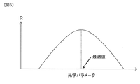
- the size of the region that darkens when the wafer potential is changed to positive is indicated by R in FIG.
- the value of the magnitude R may be determined as a magnitude of a range of image intensities smaller than the threshold by providing a constant threshold for the image intensity of the mirror electronic image. For example, the size is evaluated by counting the number of pixels in a low luminance area (pixel area below a predetermined gradation value) that is equal to or lower than a predetermined threshold.
- the size R of the darkened area is used as an evaluation index, and it is determined whether or not the optical system is adjusted so that the electron beam from the condenser lens 102 is converged to the back focal point 100b of the objective lens 106.
- FIG. 5 shows an example of a graph for this determination.
- Optical parameters are taken on the horizontal axis.
- lens conditions such as a voltage applied to the objective lens 106 and a current value applied to the condenser lens 102 (when the condenser lens 102 is a magnetic lens).
- the size R of the darkened region in the mirror electron image when the voltage of the wafer 104 is positive by a certain amount is plotted. If the darkening size is not a circle, the index is determined as the radius of a circle circumscribing the darkened area.
- FIG. 4 shows changes in points plotted in this way, and the value R takes the maximum value for a certain optical parameter value.
- An optical parameter that maximizes R or is equal to or greater than a predetermined value is set as an optimum value. At this time, the adjustment close to the situation of FIG. 4B is achieved, in which the electron beam is converged on the back focal point 100b of the objective lens 106 and the irradiated electron beam is irradiated in parallel to the normal direction of the wafer surface.
- the optical parameter of FIG. 5 is set to the voltage value of the objective lens 106
- a graph is repeatedly created for other parameters, for example, a plurality of current values of the condenser lens 102, and the objective lens 106 that gives the largest R is shown. It is also possible to determine optimum values for a plurality of optical parameters, such as selecting a combination of a voltage value and a current value of the condenser lens 102 as an optimum value.
- the state of electron beam irradiation in each apparatus Can be expressed quantitatively.
- an adjustment method using the wafer 104 is shown, but other samples are also included in the present invention as long as the surface is flat and conductive.
- a sample piece installed in a place where a wafer on the wafer holder 109 is not placed may be used.
- the negative voltage is set so that the wafer holder 109 mounted on the moving stage 108 via the insulating member 701 is at the same potential as the wafer 104 at a position different from the mounting position of the wafer 104.
- the above adjustment may be performed using a standard sample 703 that is conducted to the wafer holder 109 to which a negative voltage is applied from the applied power source 702.
- the irradiation electron beam is irradiated in parallel to the normal direction of the wafer surface without providing an electronic image observation device on the back focal plane of the objective lens. Can be evaluated quantitatively.
- FIG. 8 is a flowchart showing the process.
- the control device attached to the apparatus includes a storage medium that stores a program for operating the apparatus according to a flowchart as will be described later, and the apparatus illustrated in FIG. 1 can perform automatic adjustment of the apparatus.
- the lens condition is set to an initial value (step 801). Then, in a state where a predetermined negative voltage is applied to the sample (step 802), an image is generated by projecting a beam toward the sample, and luminance evaluation in the image is performed (step 803). In this case, pixels whose luminance value (gray level) is a predetermined value or less are counted, and the area evaluation of the low luminance region is performed. By performing such an area evaluation under a plurality of sample potential conditions, a change in the area of the low luminance region according to a change in the sample potential under a certain lens condition is evaluated.
- FIG. 9 is a diagram showing how the size of the low-luminance region 908 obtained under a plurality of lens conditions (three lens conditions (a) to (c) in this example) changes with changes in the voltage applied to the sample. is there. It shows how the sample height (depth) reached by the projected electrons changes from position 901 to 903 due to the change in the voltage applied to the sample.
- lens condition A the lens condition is weaker than the ideal value
- lens condition C lens condition is stronger than the ideal value
- changing the voltage application condition to the sample the size of each low-luminance region R A1 ⁇ It changes to R A3 , R C1 to R C3 .
- the lens condition B the lens conditions are properly set, because the beam is projected from the normal direction of the sample surface, even by changing the voltage applied to the sample, the size of the low-intensity region R B Will not change.
- the size of the low luminance region at different sample potentials is obtained for each lens condition, and the lens condition with the smallest change in the size of the low luminance region is set as the apparatus condition (step 804).
- FIG. 10 is a flowchart showing a process of evaluating the size of the low luminance region by changing the lens condition after first determining the sample potential for evaluating the low luminance region.
- the lens condition in which the size of the low luminance region is the largest (or a predetermined value or more) is an appropriate lens condition, first, to the extent that the size of the low luminance region can be evaluated. Electrons are made to reach the sample, and the size of the low luminance region is evaluated while changing the lens conditions. Therefore, after setting the initial value of the lens condition (step 1001), the luminance condition of the irradiation area (step 1003) is changed while changing the voltage condition to the sample (step 1002), thereby reducing the size of the low-luminance area.
- a moderately sized low luminance region is generated, and the lens condition is changed in that state (step 1004). Then, a lens condition that satisfies a predetermined condition for the size of the low luminance region is found (step 1004), and the lens condition is determined as an apparatus condition (step 1005). Note that after setting a predetermined number of lens conditions, the best condition may be found, or automatic adjustment may be terminated when the best condition is found. In addition, a lens condition that allows the size of the low luminance region to be maximized by interpolation may be selected.
- a device that generates an image without causing electrons to reach the sample is provided with a beam evaluation mode that allows electrons to partially reach the sample, so that inspection can be performed under appropriate beam conditions. Etc. can be performed.
- the electron beam from the condenser lens 102 is correctly aligned on the optical axis of the objective lens 106. A converged situation can be realized.
- the degree of convergence on the back focal plane 100b of the objective lens 106 may be adjusted according to the first embodiment.
- the axis of the irradiation electron optical system including the separator can be adjusted without providing an electronic image observation device on the back focal plane of the objective lens.
- FIG. 11 is a flowchart showing a process of adjusting the apparatus conditions based on the evaluation of the inclination of the beam trajectory.
- the apparatus conditions are set such that electrons can reach the sample (step 1101).
- the sample potential is changed to the positive side, and then the luminance evaluation of the irradiation region is performed (steps 1102 and 1103).
- Steps 1102 and 1103 are repeated until an image capable of evaluating the size of the low luminance region is obtained.
- a shift between the image center and the low-luminance area center is evaluated (step 1104).
- the optical axis adjustment is executed so as to correct this deviation amount (step 1105).
- an aligner deflector
- the adjustment is performed by referring to a table in which the relationship between the deviation amount and the aligner condition is stored in advance.
- the axis may be adjusted by optimizing the Wien condition of the separator 103.
- the apparatus is an apparatus that generates an image in a state where electrons do not reach the sample (first irradiation mode), and it is appropriate to provide an adjustment mode (second irradiation mode) for causing electrons to reach the sample. It is possible to find out the proper device conditions.
- the apparatus conditions are adjusted during the inspection of the actual sample or after the inspection, the electron beam is irradiated to the standard specimen 703 illustrated in FIG. 7 or an area on the wafer defined for the apparatus condition adjustment.
- the moving stage control device 107 controls the moving stage 108, and the high voltage power supply 110 changes the negative voltage applied to the wafer holder 109 to the positive side so that the irradiation electron beam 100a reaches the wafer or the standard sample.
- It is possible to perform appropriate beam evaluation and adjustment by performing image evaluation and adjustment of apparatus conditions as described above in a state where the beam has reached the wafer.
- the irradiation mode may be switched in advance by preparing an operation program (recipe) so that the apparatus switches to the second irradiation mode when the apparatus is started up or after a predetermined time has elapsed since the start of the inspection. Then, switching may be performed based on an instruction for device condition adjustment from the monitor input / output device 120.
Abstract
La présente invention concerne un appareil à faisceau de particules chargées qui effectue un ajustement d'appareil sur la base d'une évaluation appropriée d'un faisceau. A cet effet, un appareil à faisceau de particules chargées selon l'invention comprend : un système optique d'irradiation comprenant une lentille pour faire converger des faisceaux de particules chargées émis à partir d'une source de particules chargées ; et un système optique d'imagerie pour imager sur un élément d'imagerie les particules chargées obtenues par irradiation des faisceaux de particules chargées vers un échantillon, l'appareil à faisceau de particules chargées comprenant un appareil de commande pour commander la lentille, et l'appareil de commande évalue, pour chaque condition de lentille, la taille d'une zone de luminosité spécifique obtenue par le faisceau de particules chargées amenée à atteindre l'échantillon, et sélectionne la condition de lentille pour laquelle les informations de taille remplissent une condition désignée.
Priority Applications (4)
| Application Number | Priority Date | Filing Date | Title |
|---|---|---|---|
| DE112017006885.1T DE112017006885B4 (de) | 2017-03-24 | 2017-03-24 | Ladungsträgerstrahlvorrichtung und Verfahren zum Einstellen der Ladungsträgerstrahlvorrichtung |
| PCT/JP2017/011907 WO2018173241A1 (fr) | 2017-03-24 | 2017-03-24 | Appareil à faisceau de particules chargées et procédé de réglage d'appareil à faisceau de particules chargées |
| JP2019506874A JP6714147B2 (ja) | 2017-03-24 | 2017-03-24 | 荷電粒子線装置、及び荷電粒子線装置の調整方法 |
| US16/487,551 US10923315B2 (en) | 2017-03-24 | 2017-03-24 | Charged particle beam apparatus, and method of adjusting charged particle beam apparatus |
Applications Claiming Priority (1)
| Application Number | Priority Date | Filing Date | Title |
|---|---|---|---|
| PCT/JP2017/011907 WO2018173241A1 (fr) | 2017-03-24 | 2017-03-24 | Appareil à faisceau de particules chargées et procédé de réglage d'appareil à faisceau de particules chargées |
Publications (1)
| Publication Number | Publication Date |
|---|---|
| WO2018173241A1 true WO2018173241A1 (fr) | 2018-09-27 |
Family
ID=63585189
Family Applications (1)
| Application Number | Title | Priority Date | Filing Date |
|---|---|---|---|
| PCT/JP2017/011907 WO2018173241A1 (fr) | 2017-03-24 | 2017-03-24 | Appareil à faisceau de particules chargées et procédé de réglage d'appareil à faisceau de particules chargées |
Country Status (4)
| Country | Link |
|---|---|
| US (1) | US10923315B2 (fr) |
| JP (1) | JP6714147B2 (fr) |
| DE (1) | DE112017006885B4 (fr) |
| WO (1) | WO2018173241A1 (fr) |
Families Citing this family (1)
| Publication number | Priority date | Publication date | Assignee | Title |
|---|---|---|---|---|
| WO2019058440A1 (fr) * | 2017-09-20 | 2019-03-28 | 株式会社日立ハイテクノロジーズ | Dispositif à faisceau de particules chargées |
Citations (5)
| Publication number | Priority date | Publication date | Assignee | Title |
|---|---|---|---|---|
| JP2003202217A (ja) * | 2002-01-09 | 2003-07-18 | Hitachi High-Technologies Corp | パターン欠陥検査方法及びパターン欠陥検査装置 |
| JP2004227888A (ja) * | 2003-01-22 | 2004-08-12 | Jeol Ltd | ビームセパレータ |
| JP2005181246A (ja) * | 2003-12-24 | 2005-07-07 | Hitachi Ltd | パターン欠陥検査方法及び検査装置 |
| JP2007513460A (ja) * | 2003-09-05 | 2007-05-24 | カール・ツァイス・エスエムティー・アーゲー | 粒子光学システム及び装置、並びに、かかるシステム及び装置用の粒子光学部品 |
| JP2008098191A (ja) * | 2008-01-11 | 2008-04-24 | Ebara Corp | 電子線光学系の調整方法及び電子線装置 |
Family Cites Families (3)
| Publication number | Priority date | Publication date | Assignee | Title |
|---|---|---|---|---|
| JP2003331773A (ja) * | 2002-05-13 | 2003-11-21 | Jeol Ltd | 電子顕微鏡 |
| JP5127148B2 (ja) * | 2006-03-16 | 2013-01-23 | 株式会社日立ハイテクノロジーズ | イオンビーム加工装置 |
| JP5663412B2 (ja) * | 2011-06-16 | 2015-02-04 | 株式会社日立ハイテクノロジーズ | 荷電粒子線装置 |
-
2017
- 2017-03-24 WO PCT/JP2017/011907 patent/WO2018173241A1/fr active Application Filing
- 2017-03-24 US US16/487,551 patent/US10923315B2/en active Active
- 2017-03-24 DE DE112017006885.1T patent/DE112017006885B4/de active Active
- 2017-03-24 JP JP2019506874A patent/JP6714147B2/ja active Active
Patent Citations (5)
| Publication number | Priority date | Publication date | Assignee | Title |
|---|---|---|---|---|
| JP2003202217A (ja) * | 2002-01-09 | 2003-07-18 | Hitachi High-Technologies Corp | パターン欠陥検査方法及びパターン欠陥検査装置 |
| JP2004227888A (ja) * | 2003-01-22 | 2004-08-12 | Jeol Ltd | ビームセパレータ |
| JP2007513460A (ja) * | 2003-09-05 | 2007-05-24 | カール・ツァイス・エスエムティー・アーゲー | 粒子光学システム及び装置、並びに、かかるシステム及び装置用の粒子光学部品 |
| JP2005181246A (ja) * | 2003-12-24 | 2005-07-07 | Hitachi Ltd | パターン欠陥検査方法及び検査装置 |
| JP2008098191A (ja) * | 2008-01-11 | 2008-04-24 | Ebara Corp | 電子線光学系の調整方法及び電子線装置 |
Also Published As
| Publication number | Publication date |
|---|---|
| DE112017006885B4 (de) | 2022-07-14 |
| US20190378685A1 (en) | 2019-12-12 |
| JPWO2018173241A1 (ja) | 2019-12-19 |
| JP6714147B2 (ja) | 2020-06-24 |
| DE112017006885T5 (de) | 2019-10-02 |
| US10923315B2 (en) | 2021-02-16 |
Similar Documents
| Publication | Publication Date | Title |
|---|---|---|
| US9966227B2 (en) | Specimen observation method and device using secondary emission electron and mirror electron detection | |
| JP5696198B2 (ja) | 試料の検査,測定方法、及び走査電子顕微鏡 | |
| JP4248382B2 (ja) | 荷電粒子ビームによる検査方法および検査装置 | |
| JP5391252B2 (ja) | 荷電粒子ビームを用いた検査方法及び検査装置 | |
| JP4988444B2 (ja) | 検査方法および装置 | |
| JP4795883B2 (ja) | パターン検査・計測装置 | |
| WO2017158742A1 (fr) | Dispositif d'inspection de défauts | |
| US20030201393A1 (en) | Electron microscope | |
| US10229811B2 (en) | Charged particle beam inclination correction method and charged particle beam device | |
| WO2017158744A1 (fr) | Procédé d'inspection de défaut et dispositif d'inspection de défaut | |
| JP6666627B2 (ja) | 荷電粒子線装置、及び荷電粒子線装置の調整方法 | |
| JP4253576B2 (ja) | パターン欠陥検査方法及び検査装置 | |
| JP6957633B2 (ja) | 評価用半導体基板およびそれを用いた検査装置の欠陥検出感度評価方法 | |
| JP6310864B2 (ja) | 検査装置 | |
| JP6714147B2 (ja) | 荷電粒子線装置、及び荷電粒子線装置の調整方法 | |
| US10825649B2 (en) | Electron beam device | |
| JP4484860B2 (ja) | パターン欠陥検査方法 | |
| JP4334159B2 (ja) | 基板検査システムおよび基板検査方法 | |
| JP2007227116A (ja) | 電子線検査方法および装置 | |
| JP2003157784A (ja) | 荷電粒子線の測定方法、荷電粒子線走査式装置 | |
| JP2006179255A (ja) | パターン欠陥検査方法および装置 | |
| JP2018106947A (ja) | 電子線検査装置 |
Legal Events
| Date | Code | Title | Description |
|---|---|---|---|
| 121 | Ep: the epo has been informed by wipo that ep was designated in this application |
Ref document number: 17901589 Country of ref document: EP Kind code of ref document: A1 |
|
| ENP | Entry into the national phase |
Ref document number: 2019506874 Country of ref document: JP Kind code of ref document: A |
|
| 122 | Ep: pct application non-entry in european phase |
Ref document number: 17901589 Country of ref document: EP Kind code of ref document: A1 |