WO2018173154A1 - 電力変換ユニット - Google Patents
電力変換ユニット Download PDFInfo
- Publication number
- WO2018173154A1 WO2018173154A1 PCT/JP2017/011461 JP2017011461W WO2018173154A1 WO 2018173154 A1 WO2018173154 A1 WO 2018173154A1 JP 2017011461 W JP2017011461 W JP 2017011461W WO 2018173154 A1 WO2018173154 A1 WO 2018173154A1
- Authority
- WO
- WIPO (PCT)
- Prior art keywords
- radiator
- power conversion
- conversion unit
- capacitor unit
- power
- Prior art date
- Legal status (The legal status is an assumption and is not a legal conclusion. Google has not performed a legal analysis and makes no representation as to the accuracy of the status listed.)
- Ceased
Links
Images






Definitions
- the present invention relates to a power conversion unit, and more particularly to a power conversion unit that performs forced air cooling.
- a power converter applied to an uninterruptible power supply is generally a converter that converts AC power from a commercial AC power source into DC power, and an inverter that converts the DC power into AC power having a desired frequency and voltage. And.
- Each of the converter and the inverter is generally constituted by a power conversion unit including a power semiconductor element, a smoothing capacitor, a fuse, and the like.
- Patent Document 1 Japanese Patent Laid-Open No. 2006-42406
- Patent Document 1 includes a capacitor, a fuse, a radiator mounted with a power semiconductor element (IGBT: insulated gate bipolar transistor), and a fan for cooling the radiator.
- IGBT insulated gate bipolar transistor
- the present invention has been made to solve such problems, and an object of the present invention is to provide a power conversion unit capable of efficiently cooling a semiconductor element.
- the power conversion unit includes a plurality of semiconductor elements, a radiator, a capacitor unit, and a housing.
- the plurality of semiconductor elements constitute a power converter.
- a radiator mounts a plurality of semiconductor elements and performs heat exchange with the semiconductor elements.
- the capacitor unit is electrically connected in parallel with the power converter, and smoothes the output voltage of the power converter.
- the housing accommodates a plurality of semiconductor elements, a radiator and a capacitor unit.
- An exhaust hole and a first intake hole are formed in the housing.
- the radiator is disposed in a ventilation path formed between the exhaust hole and the first intake hole.
- the capacitor unit is disposed on the upstream side of the radiator in the ventilation path.
- a second intake hole is further formed in a portion of the housing located between the radiator and the capacitor unit.
- FIG. 3 is a top view showing a configuration of a power conversion unit according to the first embodiment.
- FIG. 7 is a top view showing a configuration of a power conversion unit according to a second embodiment.
- FIG. 11 is a circuit diagram of a power conversion unit according to a third embodiment. It is a side view which shows the structure of the power conversion unit according to Embodiment 3.
- FIG. 10 is a top view showing a configuration of a power conversion unit according to a third embodiment.
- FIG. 1 is a circuit diagram of the power conversion unit.
- FIG. 1 shows a circuit diagram of an inverter unit as a typical example of the power conversion unit.
- the inverter unit 5 converts DC power into AC power.
- inverter unit 5 includes DC positive bus PL, DC negative bus NL, capacitor unit 1, inverter 4, and fuse 6.
- the capacitor unit 1 is connected between the DC positive bus PL and the DC negative bus NL.
- the capacitor unit 1 is electrically connected in parallel to the inverter 4 and smoothes the output voltage of the inverter 4.
- Capacitor unit 1 includes a plurality of DC smoothing electrolytic capacitors.
- the inverter 4 includes a plurality of power modules 40 connected in parallel between the DC positive bus PL and the DC negative bus NL.
- Each power module 40 includes two IGBTs 401 connected in series between DC input nodes P and L, and two anti-parallel diodes (hereinafter referred to as diodes) 402 respectively connected to the two IGBTs 401.
- diodes two anti-parallel diodes
- the inverter 4 is described as a so-called two-level inverter, but is not limited to this, and may be, for example, a three-level inverter.
- the load 2 is driven by three-phase AC power output from the nodes U, V, and W connected to the connection points of the two IGBTs 401 of the power module 40.
- the load 2 is, for example, a motor.
- the fuse 6 is electrically connected to at least one of the DC input node P and the DC positive bus PL of the power module 40 and between the DC input node N and the DC negative bus NL of the power module 40.
- the fuse 6 is provided for short-circuit protection when the IGBT 401 or the diode 402 is short-circuited for some reason.
- a radiator is used for the heat radiation.
- Fig. 2 is an external view of a typical radiator.
- the radiator 7 includes a heat receiving portion 71 and a fin portion 72.
- the fin part 72 has a plurality of blades (fins) arranged in a first direction 55 perpendicular to the ventilation direction of the cooling air 50 flowing in the ventilation path described later.
- the cooling air 50 and the first direction 55 are indicated by arrows 50 and 55 in FIG. 2, respectively.
- the power module 40 is mounted on the upper surface of the heat receiving unit 71.
- the heat receiving unit 71 is configured to exchange heat with the power module 40. As shown in FIG. 2, the power module 40 on the heat receiving unit 71 is arranged in parallel in the first direction 55.
- the heat of the power module 40 is transmitted to the fin portion 72 through the heat receiving portion 71.
- the power module 40 is cooled by heat exchange between the cooling air 50 and the fins 72.
- the power conversion unit according to the comparative example includes a capacitor unit 1, an inverter 4, a radiator 7, a fuse 6, a bus bar 10, and a housing 3 that houses the above-described components.
- Capacitor unit 1 includes a plurality of capacitors 1a.
- the housing 3 is a rectangular parallelepiped including a bottom surface 3a, a top surface 3b facing the bottom surface 3a, and side surfaces 3c to 3f intersecting the bottom surface 3a and the top surface 3b.
- An exhaust hole 30 is formed in one side surface 3 c of the housing 3.
- An exhaust fan 9 is provided in the exhaust hole 30.
- the fan 9 is configured to discharge the air in the housing 3 to the outside of the housing 3.
- the housing 3 is formed with an intake hole 31 a on the side opposite to the fan 9 with respect to the radiator 7.
- the intake hole 31a corresponds to an example of a “first intake hole”.
- the intake holes 31a are formed in the side surface 3d in FIGS.
- cooling air 51 an air flow (wind) from the intake hole 31 a to the exhaust hole 30 is generated in the housing 3 by the fan 9.
- the wind from the intake hole 31 a to the exhaust hole 30 is referred to as cooling air 51.
- the cooling air 51 is indicated by an arrow 51 in FIGS.
- the radiator 7 (the heat receiving portion 71 and the fin portion 72) is disposed in the ventilation path formed between the exhaust hole 30 and the intake hole 31a, and the capacitor unit 1 is disposed upstream of the radiator 7 in the ventilation path. Be placed.
- the capacitor unit 1, the fuse 6, and the radiator 7 are arranged in this order from the upstream side to the downstream side of the cooling air 51.
- the power module 40 mounted on the capacitor unit 1, the fuse 6, and the radiator 7 is electrically connected by the bus bar 10.
- Bus bar 10 constitutes DC positive bus PL and DC negative bus NL in FIG.
- the cooling air 51 passes through the radiator 7 after passing through the capacitor unit 1 and the fuse 6. For this reason, when passing through the radiator 7, the heat of the capacitor unit 1 and the fuse 6 may be taken and the temperature of the cooling air may be increased. Further, the wind force of the cooling air may be weakened by the ventilation resistance of the capacitor unit 1 and the fuse 6. For these reasons, there is a concern that the cooling capacity of the cooling air 51 supplied to the radiator 7 is weakened.
- the first embodiment by forming a hole in the housing portion located between the capacitor unit 1 and the radiator 7, it does not pass through the capacitor unit 1 and the fuse 6, and directly the radiator 7.
- the cooling air supplied to is generated, and the cooling efficiency of the radiator 7 is increased.
- FIGS. 5 and 6 are a side view and a top view, respectively, showing the configuration of the power conversion unit according to the first embodiment.
- the power conversion unit according to the first embodiment is different from the power conversion unit according to the comparative example in that the portion of housing 3 located between capacitor unit 1 and radiator 7 is inhaled. That is, the hole 32 is formed.
- the intake hole 32 corresponds to an example of a “second intake hole”.
- the intake holes 32 are formed in the bottom surface 3a in FIGS.
- cooling air can be introduced into the housing 3 from the air intake holes 32 in addition to the air intake holes 31a.
- cooling air 52 the cooling air from the intake hole 32 to the exhaust hole 30 is referred to as cooling air 52.
- the cooling air 52 is indicated by an arrow 52 in FIGS.
- the cooling air 52 is supplied directly to the radiator 7 without passing through the capacitor unit 1 and the fuse 6. That is, the cooling air 52 supplied to the radiator 7 is hardly subjected to the temperature rise and the wind power decrease caused by the capacitor unit 1 and the fuse 6, and therefore the cooling efficiency of the radiator 7 is higher than that of the cooling air 51. That is, the power module 40 mounted on the radiator 7 can be efficiently cooled using the cooling air 52.
- a part of the cooling air 52 is directly supplied to the fuse 6. .
- a fuse tends to become high temperature because it generates heat according to its resistance. Therefore, it is preferable that a part of the cooling air 52 is directly supplied to the fuse 6 in terms of cooling the fuse 6 and preventing damage due to heat.
- the housing 3 is described as a rectangular parallelepiped, but the shape of the housing 3 is not limited to this.
- the exhaust hole 30 is described as being formed on one side surface 3c of the housing 3, and the intake hole 31a is formed on the opposite side surface 3d.
- the exhaust hole 30 and the intake hole 31a are The position is not limited to this, and may be a position that sandwiches the radiator 7, that is, a position that can supply cooling air to the radiator 7.
- the position of the first hole may be the side surfaces 3e and 3f as in the intake hole 31b in FIG.
- the intake hole 32 is described as being formed in the bottom surface 3 a of the housing 3.
- the position of the intake hole 32 is not limited to this, and the capacitor unit 1 and the radiator 7
- the portion of the housing located between them may be a location suitable for introducing air into the housing 3.
- the side surfaces 3 e and 3 f of the housing 3 may be used.
- the fan 9 is provided in the exhaust hole 30.
- the present invention is not limited to this, and a ventilation path is formed between the exhaust hole 30 and each of the intake holes 31 a, 31 b, 32. Any configuration may be used.
- the hole is formed in the portion of the housing located between the capacitor and the radiator, so that the capacitor is introduced from the hole.
- the semiconductor element can be efficiently cooled by the cooling air that is not. That is, a power conversion unit capable of efficiently cooling a semiconductor element can be provided.
- FIG. 7 is a top view showing the configuration of the power conversion unit according to the second embodiment of the present invention. 6 and 7, the power conversion unit according to the second embodiment is different from the power conversion unit according to the first embodiment in the interval between the plurality of capacitors 1 a included in the capacitor unit 1.
- the capacitors 1a are roughly arranged. Specifically, the capacitors 1a are arranged in a first direction 55 perpendicular to the ventilation direction, and the interval W2 between two capacitors adjacent to the first direction 55 is increased.
- the first direction 55 is indicated by an arrow 55.
- the cooling air 53 from the intake hole 31a which is indicated by the arrow 53 in FIG. Easy to be supplied.
- the above effect can be easily realized by configuring the interval W2 between the capacitors 1a adjacent to each other in the first direction 55 to be wider than the interval W1 between the fins of the fin portion 72 of the radiator 7.
- the interval W3 between the two capacitors 1a adjacent in the second direction 56 parallel to the ventilation direction. Also, it may be configured to expand.
- the second direction 56 is indicated by an arrow 56.
- the power conversion unit according to the second embodiment has the same functions and effects as those of the first embodiment.
- Other configurations are the same as those in the first embodiment, and thus description thereof will not be repeated.
- FIG. 9 is a top view showing the configuration of the power conversion unit according to the third embodiment of the present invention. 1 and 9, the power conversion unit according to the third embodiment is different from the power conversion unit according to the first embodiment in the electrical connection relationship of capacitor unit 1, power module 40, and fuse 6. ing.
- FIG. 9 is a circuit diagram of the power conversion unit according to the third embodiment.
- capacitor unit 1 is electrically connected in parallel between DC input node P and DC input node N of each power module 40.
- the fuse 6 is electrically connected between the node ND1 between the DC input node P of the power module 40 and the capacitor unit 1 and the DC positive bus PL. Even in such a configuration, as in the first embodiment, the fuse 6 functions as a short circuit protection when the IGBT 401 or the diode 402 is short-circuited for some reason.
- 10 and 11 are a side view and a top view showing the configuration of the power conversion unit according to the third embodiment.
- fuse 6 is connected to the opposite side of power module 40 to node ND ⁇ b> 1 between power module 40 and capacitor unit 1 on bus bar 10.
- the fuse 6 is arranged between the radiator 7 and the capacitor unit 1 inside the housing 3 as in the first embodiment.
- a part of the cooling air 52 can be directly supplied to the fuse 6 to prevent the fuse 6 from being damaged by heat.
- the power conversion unit according to the third embodiment has the same functions and effects as those of the first embodiment.
- Other configurations are the same as those in the first embodiment, and thus description thereof will not be repeated.
- IGBT Power semiconductor element
Landscapes
- Inverter Devices (AREA)
Abstract
複数の半導体素子は、電力変換器(4)を構成する。放熱器(71,72)は、複数の半導体素子を搭載し、半導体素子と熱交換を行なう。コンデンサユニット(1)は、電力変換器(4)と電気的に並列に接続され、電力変換器(4)の出力電圧を平滑化する。ヒューズ(6)は、電力線(10)に介挿される。筐体(3)は、複数の半導体素子、放熱器(71,72)およびコンデンサユニット(1)を収容する。筐体(3)には、排気孔(30)と第1の吸気孔(31a)が形成される。放熱器(71,72)は、排気孔(30)と第1の吸気孔(31a)との間に形成される通風路(51)に配置される。コンデンサユニット(1)は、通風路(51)における放熱器(71,72)の上流側に配置される。放熱器(71,72)とコンデンサユニット(1)との間に位置する筐体(3)の部分には、第2の吸気孔(32)がさらに形成される。
Description
この発明は、電力変換ユニットに関し、特に、強制風冷を行なう電力変換ユニットに関する。
無停電電源装置などに適用される電力変換装置は、一般的に、商用交流電源からの交流電力を直流電力に変換するコンバータと、その直流電力を所望の周波数および電圧の交流電力に変換するインバータとを備えている。コンバータおよびインバータの各々は、通常、電力用半導体素子、平滑用コンデンサ、ヒューズ等を含む電力変換ユニットで構成される。
上記半導体素子は、スイッチング動作時の発生損失により発熱し、また、該発熱により損傷する可能性があるため、放熱することが必要になる。たとえば、特開2006-42406号公報(特許文献1)には、コンデンサと、ヒューズと、電力用半導体素子(IGBT:insulated Gate Bipolar Transistor)を搭載した放熱器と、放熱器冷却用のファンとが上記の順に並べられた電力変換装置の構造が開示されている。このような構造においては、上記ファンからの強制排気により生成される風が、コンデンサ、ヒューズ、放熱器の順に通過し、放熱器に搭載されたIGBTを冷却する。
しかしながら、特許文献1に記載される電力変換装置の構造では、放熱器に供給される冷却風は、既にコンデンサおよびヒューズを通過しているため、コンデンサおよびヒューズの熱を奪い温度が上昇している可能性があった。また、コンデンサおよびヒューズの通風抵抗により放熱器に供給される冷却風の風力が減衰している可能性があった。すなわち、特許文献1では、半導体素子を搭載した放熱器が充分に冷却されず、半導体素子が損傷する可能性があった。
この発明は、このような問題点を解決するためになされたものであって、この発明の目的は、効率良く半導体素子を冷却することができる電力変換ユニットを提供することである。
この発明のある局面に従えば、電力変換ユニットは、複数の半導体素子と、放熱器と、コンデンサユニットと、筐体とを備える。複数の半導体素子は、電力変換器を構成する。放熱器は、複数の半導体素子を搭載し、半導体素子と熱交換を行なう。コンデンサユニットは、電力変換器と電気的に並列に接続され、電力変換器の出力電圧を平滑化する。筐体は、複数の半導体素子、放熱器およびコンデンサユニットを収容する。筐体には、排気孔および第1の吸気孔が形成される。放熱器は、排気孔と第1の吸気孔との間に形成される通風路に配置される。コンデンサユニットは、通風路における放熱器の上流側に配置される。放熱器とコンデンサユニットとの間に位置する筐体の部分には、第2の吸気孔がさらに形成される。
この発明によれば、効率良く半導体素子を冷却することができる電力変換ユニットを提供することができる。
以下、本発明の実施の形態について、図面を参照しながら詳細に説明する。なお、図中の同一または相当部分には同一符号を付してその説明は繰返さない。
図1は、電力変換ユニットの回路図である。図1では電力変換ユニットの代表例としてインバータユニットの回路図を示す。インバータユニット5は、直流電力を交流電力に変換する。図1を参照して、インバータユニット5は、直流正母線PL、直流負母線NL、コンデンサユニット1、インバータ4、およびヒューズ6を備える。
コンデンサユニット1は、直流正母線PLおよび直流負母線NLの間に接続されている。コンデンサユニット1は、インバータ4と電気的に並列に接続され、インバータ4の出力電圧を平滑化する。コンデンサユニット1は、複数の直流平滑用電解コンデンサを含む。
インバータ4は、直流正母線PLおよび直流負母線NLの間に並列に接続される複数のパワーモジュール40を含む。各パワーモジュール40は、直流入力ノードP,Lの間に直列に接続された2つのIGBT401と、2つのIGBT401にそれぞれ接続された2つの逆並列ダイオード(以下、ダイオードと称する)402とを有する。なお、図1では、インバータ4は、いわゆる2レベルインバータとして記載されているが、これに限定されるものではなく、たとえば3レベルインバータであってもよい。
負荷2は、パワーモジュール40の2つのIGBT401の接続点に接続されるノードU,V,Wから出力される三相交流電力で駆動される。負荷2は、たとえばモータである。
ヒューズ6は、パワーモジュール40の直流入力ノードPと直流正母線PLとの間、および、パワーモジュール40の直流入力ノードNと直流負母線NLとの間の少なくとも一方に電気的に接続される。ヒューズ6はIGBT401またはダイオード402が何らかの原因でショートしたときの短絡保護用として設けられる。
IGBT401はスイッチング動作時の損失により発熱するため、放熱が必要である。該放熱のためには、放熱器が用いられる。
図2は、代表的な放熱器の外観図である。図2を参照して、放熱器7は、受熱部71とフィン部72とを備える。
フィン部72は、後述する通風路に流れる冷却風50の通風方向に垂直な第1の方向55に並んだ複数の羽根(フィン)を有する。冷却風50および第1の方向55は、図2ではそれぞれ矢印50および矢印55で示される。受熱部71の上面には、パワーモジュール40が搭載される。受熱部71はパワーモジュール40と熱交換を行なうように構成される。受熱部71上のパワーモジュール40は、図2に示すように、第1の方向55に並列に配置される。
パワーモジュール40の熱は、受熱部71を通じてフィン部72に伝わる。冷却風50とフィン部72との熱交換により、パワーモジュール40が冷却される。
次に、図3および図4を用いて、比較例として、従来の電力変換ユニットの構成を説明する。
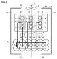
図3および図4は、それぞれ、比較例による電力変換ユニットの構成を示す側面図および上面図である。図3および図4を参照して、比較例による電力変換ユニットは、コンデンサユニット1、インバータ4、放熱器7、ヒューズ6、バスバー10、および上記構成要素を収容する筐体3を備える。コンデンサユニット1は、複数のコンデンサ1aを含む。
筐体3は、底面3aと、底面3aに対向する上面3bと、底面3aおよび上面3bと交差する側面3c~3fとを含む直方体である。筐体3の1つの側面3cには排気孔30が形成される。排気孔30には排気用のファン9が設けられる。ファン9は、筐体3内の空気を筐体3外に排出するように構成される。また、筐体3には、放熱器7に対してファン9と反対側に吸気孔31aが形成される。吸気孔31aは「第1の吸気孔」の一実施例に対応する。吸気孔31aは、図3,4では側面3dに形成される。その結果、筐体3内には、ファン9により、吸気孔31aから排気孔30に向かう空気の流れ(風)が生成される。以下、吸気孔31aから排気孔30への風を冷却風51と称する。冷却風51は、図3,4では矢印51で示される。
放熱器7(受熱部71およびフィン部72)は、排気孔30と吸気孔31aとの間に形成される通風路に配置され、コンデンサユニット1は、該通風路における放熱器7の上流側に配置される。換言すると、筐体3内には、冷却風51の上流側から下流側に、コンデンサユニット1、ヒューズ6、放熱器7がこの順に並べられる。コンデンサユニット1、ヒューズ6、放熱器7上に搭載されるパワーモジュール40はバスバー10で電気的に接続されている。バスバー10は、図1の直流正母線PLおよび直流負母線NLを構成する。
冷却風51は、コンデンサユニット1およびヒューズ6を通過した後に、放熱器7を通過する。このため、放熱器7を通過するときには、コンデンサユニット1およびヒューズ6の熱を奪い冷却風の温度が上がっている可能性がある。また、コンデンサユニット1およびヒューズ6の通風抵抗により冷却風の風力が弱められている可能性がある。これらの理由により、放熱器7に供給される冷却風51の冷却能力が弱められていることが懸念される。
ゆえに、本実施の形態1においては、コンデンサユニット1と放熱器7との間に位置する筐体の部分に孔を形成することで、コンデンサユニット1およびヒューズ6を通過せず、直接放熱器7に供給される冷却風を生成し、放熱器7の冷却効率を上げる。
[実施の形態1]
図5および図6は、それぞれ、実施の形態1に従う電力変換ユニットの構成を示す側面図および上面図である。図5,6を参照して、実施の形態1に従う電力変換ユニットが、比較例に従う電力変換ユニットと異なる点は、コンデンサユニット1と放熱器7との間に位置する筐体3の部分に吸気孔32が形成されていることである。吸気孔32は「第2の吸気孔」の一実施例に相当する。吸気孔32は、図5,6では底面3aに形成される。
図5および図6は、それぞれ、実施の形態1に従う電力変換ユニットの構成を示す側面図および上面図である。図5,6を参照して、実施の形態1に従う電力変換ユニットが、比較例に従う電力変換ユニットと異なる点は、コンデンサユニット1と放熱器7との間に位置する筐体3の部分に吸気孔32が形成されていることである。吸気孔32は「第2の吸気孔」の一実施例に相当する。吸気孔32は、図5,6では底面3aに形成される。
本実施の形態1では、吸気孔31aに加え、吸気孔32からも筐体3内部に冷却風を導入することができる。以下、吸気孔32から排気孔30への冷却風を冷却風52と称する。冷却風52は、図5,6では矢印52で示される。
冷却風52の大部分は、コンデンサユニット1およびヒューズ6を通過せず、直接放熱器7に供給される。すなわち、放熱器7に供給される冷却風52は、コンデンサユニット1およびヒューズ6による温度上昇および風力の低下をほとんど受けていないので、冷却風51に比べ、放熱器7の冷却効率が高い。すなわち、冷却風52を用いて、効率的に放熱器7上に搭載されるパワーモジュール40を冷却できる。
また、図5,6に示すように、ヒューズ6を筐体3内部の、放熱器7とコンデンサユニット1との間に設置すれば、冷却風52の一部はヒューズ6にも直接供給される。一般に、ヒューズはその抵抗に応じて発熱するので高温になりやすい傾向がある。よって、ヒューズ6に冷却風52の一部が直接供給されることは、ヒューズ6を冷却し、熱による破損を防ぐという点で好ましい。
なお、図5および図6では、筐体3を直方体として記載したが、筐体3の形はこれに限定されない。また、図5および図6では、排気孔30を筐体3の1つの側面3cに、吸気孔31aを反対側の側面3dに形成されるように記載したが、排気孔30および吸気孔31aの位置はこれに限定されず、放熱器7を挟む位置、すなわち、放熱器7に冷却風を供給できる位置であればよい。たとえば、第1の孔の位置は、図6の吸気孔31bのように、側面3e,3fでもよい。また、図5および図6では、吸気孔32を筐体3の底面3aに形成されるように記載したが、吸気孔32の位置はこれに限定されず、コンデンサユニット1と放熱器7との間に位置する筐体の部分で、筐体3内への空気の導入に適した箇所であればよく、たとえば筐体3の側面3e,3fでもよい。なお、図5および図6では、ファン9を排気孔30に設けているが、これに限定されず、排気孔30と各吸気孔31a,31b,32との間に通風路が形成されるような構成であればよい。
このように、本実施の形態1に従う電力変換ユニットによれば、コンデンサと放熱器との間に位置する筐体の部分に孔が形成されることで、該孔から導入される、コンデンサを経由しない冷却風により、半導体素子を効率的に冷却することができる。すなわち、効率良く半導体素子を冷却することができる電力変換ユニットを提供できる。
[実施の形態2]
図7は、本発明の実施の形態2に従う電力変換ユニットの構成を示す上面図である。図6および図7を比較して、実施の形態2に従う電力変換ユニットは、コンデンサユニット1に含まれる複数のコンデンサ1aの間隔が、実施の形態1に従う電力変換ユニットとは異なっている。
図7は、本発明の実施の形態2に従う電力変換ユニットの構成を示す上面図である。図6および図7を比較して、実施の形態2に従う電力変換ユニットは、コンデンサユニット1に含まれる複数のコンデンサ1aの間隔が、実施の形態1に従う電力変換ユニットとは異なっている。
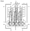
具体的には、図6に示すように、実施の形態1では、複数のコンデンサ1aは密に並べられ、コンデンサ1a同士の間隔は空いていない。そのため、冷却風51が放熱器7に供給されにくい場合がある。これに対して、図7に示すように、実施の形態2では、コンデンサ1aは粗に並べられている。具体的にはコンデンサ1aが通風方向に対して垂直な第1の方向55に並べて配置され、第1の方向55に隣接する2つのコンデンサの間隔W2が拡げられている。図6では、第1の方向55は矢印55で示されている。このことにより、実施の形態2では、実施の形態1に比べ、図6で矢印53で示す、吸気孔31aからの冷却風53がコンデンサ1a間を通りやすいため、冷却風53が放熱器7に供給されやすい。特に、第1の方向55に隣り合うコンデンサ1aの間隔W2を、放熱器7のフィン部72の各フィンの間隔W1より広く構成することで、上記効果は実現しやすい。
また、図8に示すように、第1の方向55に隣接する2つのコンデンサ1aの間隔W2を拡げることに加え、通風方向に平行な第2の方向56に隣接する2つのコンデンサ1aの間隔W3も拡げるように構成してもよい。図6では、第2の方向56は矢印56で示されている。
以上のように、実施の形態2に従う電力変換ユニットは、実施の形態1と同様の作用効果を有する。他の構成については、実施の形態1と同様であるので説明をくり返さない。
[実施の形態3]
図9は、本発明の実施の形態3に従う電力変換ユニットの構成を示す上面図である。図1および図9を比較して、実施の形態3に従う電力変換ユニットは、コンデンサユニット1、パワーモジュール40、およびヒューズ6の電気的な接続関係が、実施の形態1に従う電力変換ユニットとは異なっている。
図9は、本発明の実施の形態3に従う電力変換ユニットの構成を示す上面図である。図1および図9を比較して、実施の形態3に従う電力変換ユニットは、コンデンサユニット1、パワーモジュール40、およびヒューズ6の電気的な接続関係が、実施の形態1に従う電力変換ユニットとは異なっている。
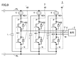
図9は、実施の形態3に従う電力変換ユニットの回路図である。図9を参照して、コンデンサユニット1は、各パワーモジュール40の直流入力ノードPと直流入力ノードNとの間に電気的に並列接続される。換言すると、ヒューズ6は、パワーモジュール40の直流入力ノードPとコンデンサユニット1との間のノードND1と、直流正母線PLとの間に電気的に接続される。このような構成においても、実施の形態1と同様に、ヒューズ6はIGBT401またはダイオード402が何らかの原因でショートしたときの短絡保護の機能を果たす。
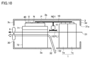
図10および図11は、実施の形態3に従う電力変換ユニットの構成を示す側面図および上面図である。図10を参照して、ヒューズ6は、バスバー10上のパワーモジュール40とコンデンサユニット1との間にあるノードND1に対し、パワーモジュール40の反対側に接続される。そして、ヒューズ6は、実施の形態1と同様に、筐体3内部の、放熱器7とコンデンサユニット1との間に配置される。その結果、実施の形態1と同様に、ヒューズ6に冷却風52の一部を直接供給し、ヒューズ6の熱による破損を防ぐことができる。
以上のように、実施の形態3に従う電力変換ユニットは、実施の形態1と同様の作用効果を有する。他の構成については、実施の形態1と同様であるので説明をくり返さない。
今回開示された実施の形態はすべての点で例示であって制限的なものではないと考えられるべきである。本発明の範囲は上記した説明ではなくて請求の範囲によって示され、請求の範囲と均等の意味および範囲内でのすべての変更が含まれることが意図される。
1 コンデンサユニット、1a コンデンサ、2 負荷、3 筐体、3a 底面、3b 上面、3c~3f 側面、4 インバータ、5 インバータユニット、6 ヒューズ、7 放熱器、9 ファン、10 バスバー、30 排気孔、31a,31b,32 吸気孔、40 パワーモジュール、50,51,52,53 冷却風、71 受熱部、72 フィン部、401 電力用半導体素子(IGBT)、402 ダイオード、N,P 直流入力ノード、NL 直流負母線、PL 直流正母線、U,V,W,ND1 ノード。
Claims (5)
- 複数の半導体素子を含む電力変換器と、
前記複数の半導体素子を搭載し、前記半導体素子と熱交換を行なう放熱器と、
前記電力変換器と電気的に並列に接続され、前記電力変換器の出力電圧を平滑化するコンデンサユニットと、
前記複数の半導体素子、前記放熱器および前記コンデンサユニットを収容する筐体とを備え、
前記筐体には、排気孔および第1の吸気孔が形成され、
前記放熱器は、前記排気孔と前記第1の吸気孔との間に形成される通風路に配置され、
前記コンデンサユニットは、前記通風路における前記放熱器の上流側に配置され、
前記放熱器と前記コンデンサユニットとの間に位置する前記筐体の部分には、第2の吸気孔がさらに形成される、電力変換ユニット。 - 前記コンデンサユニットは、複数のコンデンサを含み、
前記放熱器は、前記通風路に流れる冷却風の通風方向に垂直な第1の方向に並べられた複数のフィンを含み、
前記複数のコンデンサは前記第1の方向に並べて配置され、前記第1の方向に隣接する前記コンデンサの間隔は、隣接する前記フィンの間隔より広い、請求項1に記載の電力変換ユニット。 - 前記電力変換器は、直流正母線および直流負母線の間に並列に接続される複数のパワーモジュールを含み、
前記電力変換ユニットは、各前記複数のパワーモジュールと前記直流正母線および前記直流負母線の少なくとも一方との間に電気的に接続されるヒューズをさらに備え、
前記ヒューズは、前記放熱器と前記コンデンサユニットとの間に配置される、請求項1または2に記載の電力変換ユニット。 - 前記コンデンサユニットは、前記直流正母線および前記直流負母線の間に接続される、請求項3に記載の電力変換ユニット。
- 前記コンデンサユニットは、各前記複数のパワーモジュールと並列に接続される、請求項3に記載の電力変換ユニット。
Priority Applications (1)
| Application Number | Priority Date | Filing Date | Title |
|---|---|---|---|
| PCT/JP2017/011461 WO2018173154A1 (ja) | 2017-03-22 | 2017-03-22 | 電力変換ユニット |
Applications Claiming Priority (1)
| Application Number | Priority Date | Filing Date | Title |
|---|---|---|---|
| PCT/JP2017/011461 WO2018173154A1 (ja) | 2017-03-22 | 2017-03-22 | 電力変換ユニット |
Publications (1)
| Publication Number | Publication Date |
|---|---|
| WO2018173154A1 true WO2018173154A1 (ja) | 2018-09-27 |
Family
ID=63585060
Family Applications (1)
| Application Number | Title | Priority Date | Filing Date |
|---|---|---|---|
| PCT/JP2017/011461 Ceased WO2018173154A1 (ja) | 2017-03-22 | 2017-03-22 | 電力変換ユニット |
Country Status (1)
| Country | Link |
|---|---|
| WO (1) | WO2018173154A1 (ja) |
Citations (3)
| Publication number | Priority date | Publication date | Assignee | Title |
|---|---|---|---|---|
| JP2006042406A (ja) * | 2004-07-22 | 2006-02-09 | Fuji Electric Fa Components & Systems Co Ltd | 電力変換装置のスタック構造 |
| JP2007115844A (ja) * | 2005-10-19 | 2007-05-10 | Yaskawa Electric Corp | モータ制御装置 |
| JP2007274765A (ja) * | 2006-03-30 | 2007-10-18 | Toshiba Mitsubishi-Electric Industrial System Corp | 電力変換装置 |
-
2017
- 2017-03-22 WO PCT/JP2017/011461 patent/WO2018173154A1/ja not_active Ceased
Patent Citations (3)
| Publication number | Priority date | Publication date | Assignee | Title |
|---|---|---|---|---|
| JP2006042406A (ja) * | 2004-07-22 | 2006-02-09 | Fuji Electric Fa Components & Systems Co Ltd | 電力変換装置のスタック構造 |
| JP2007115844A (ja) * | 2005-10-19 | 2007-05-10 | Yaskawa Electric Corp | モータ制御装置 |
| JP2007274765A (ja) * | 2006-03-30 | 2007-10-18 | Toshiba Mitsubishi-Electric Industrial System Corp | 電力変換装置 |
Similar Documents
| Publication | Publication Date | Title |
|---|---|---|
| JP5269259B2 (ja) | 電力変換装置 | |
| CN101681898B (zh) | 半导体元件的冷却构造 | |
| JP5212088B2 (ja) | 半導体モジュール冷却装置 | |
| JP4506848B2 (ja) | 半導体モジュール | |
| JP5354083B2 (ja) | 半導体装置 | |
| JP6429721B2 (ja) | 電力変換装置及び鉄道車両 | |
| JP6977743B2 (ja) | 電力変換装置 | |
| JP2016072330A (ja) | 発熱体の冷却構造、電力変換器ユニットおよび電力変換装置 | |
| CN113632364B (zh) | 电力变换单元 | |
| US20200068749A1 (en) | Cooling structure of power conversion device | |
| US9532489B2 (en) | Power conversion device | |
| US12408310B2 (en) | Power converter, heat exchanger, heat sink, and photovoltaic power generation system | |
| US20170117820A1 (en) | Semiconductor device | |
| JP6594290B2 (ja) | 電力変換装置 | |
| JP6074346B2 (ja) | 配電盤装置 | |
| JP5787105B2 (ja) | 電力変換装置 | |
| CN102611327B (zh) | 功率转换器的层叠结构 | |
| CN102683303A (zh) | 半导体装置 | |
| JP2012212776A (ja) | 電力変換装置 | |
| JP6174824B2 (ja) | 電力変換装置 | |
| CN111034007A (zh) | 电力变换装置 | |
| WO2018173154A1 (ja) | 電力変換ユニット | |
| JP6868322B2 (ja) | 電力変換装置 | |
| JP7234845B2 (ja) | コンデンサユニット | |
| JP6362959B2 (ja) | 電力変換回路、その製造方法、および、パワーコンディショナ |
Legal Events
| Date | Code | Title | Description |
|---|---|---|---|
| 121 | Ep: the epo has been informed by wipo that ep was designated in this application |
Ref document number: 17902146 Country of ref document: EP Kind code of ref document: A1 |
|
| NENP | Non-entry into the national phase |
Ref country code: DE |
|
| 122 | Ep: pct application non-entry in european phase |
Ref document number: 17902146 Country of ref document: EP Kind code of ref document: A1 |
|
| NENP | Non-entry into the national phase |
Ref country code: JP |