WO2018167871A1 - 半導体装置 - Google Patents
半導体装置 Download PDFInfo
- Publication number
- WO2018167871A1 WO2018167871A1 PCT/JP2017/010389 JP2017010389W WO2018167871A1 WO 2018167871 A1 WO2018167871 A1 WO 2018167871A1 JP 2017010389 W JP2017010389 W JP 2017010389W WO 2018167871 A1 WO2018167871 A1 WO 2018167871A1
- Authority
- WO
- WIPO (PCT)
- Prior art keywords
- electrode
- short
- gate
- region
- semiconductor region
- Prior art date
- Legal status (The legal status is an assumption and is not a legal conclusion. Google has not performed a legal analysis and makes no representation as to the accuracy of the status listed.)
- Ceased
Links
Images
Classifications
-
- H—ELECTRICITY
- H10—SEMICONDUCTOR DEVICES; ELECTRIC SOLID-STATE DEVICES NOT OTHERWISE PROVIDED FOR
- H10D—INORGANIC ELECTRIC SEMICONDUCTOR DEVICES
- H10D18/00—Thyristors
Definitions
- the present invention relates to a semiconductor device, and more particularly to a semiconductor device that conducts between an anode electrode and a cathode electrode by passing a current through a gate electrode.
- Patent Document 1 a corner gate thyristor in which a gate electrode is formed at a corner portion of a rectangular semiconductor region is known as a kind of thyristor (see Patent Document 1).
- Dv / dt resistance is one of the characteristics of thyristors.
- the dv / dt resistance indicates the ease of malfunction of the thyristor. If this value is small, the thyristor may be turned on erroneously.
- a P-type semiconductor region that penetrates an N-type emitter region formed in a P-type base region (hereinafter referred to as “short gate” in the present application), like the thyristor described in Patent Document 1. (Referred to as Short Gate: SG).
- the short gate is a resistor provided in parallel with the N-type emitter region.
- a current (charging current) for charging the junction capacitance in the semiconductor device to which the reverse bias is applied flows to the cathode electrode through the short gate. For this reason, the amount of electrons injected from the N-type emitter region into the P-type base region is reduced, and the thyristor can maintain the off state even when a steep voltage is applied. As a result, the dv / dt resistance is improved.
- the dv / dt tolerance and the gate trigger current (I GT ) are positively correlated. For this reason, when the number of short gates is increased to increase the dv / dt tolerance, there is a problem that the gate trigger current (I GT ) also increases (that is, the on characteristic changes greatly).
- an object of the present invention is to provide a semiconductor device capable of increasing the dv / dt resistance without greatly affecting the on-characteristics.
- a semiconductor device includes: A first conductivity type semiconductor substrate having a first main surface and a second main surface opposite to the first main surface; A first semiconductor region of a second conductivity type formed on the first main surface of the semiconductor substrate; A second semiconductor region of a first conductivity type formed in the first semiconductor region; A third semiconductor region of a second conductivity type formed on the second main surface of the semiconductor substrate; A gate electrode formed on the first main surface so as to be electrically connected to the first semiconductor region; A first main electrode formed on the first main surface so as to be electrically connected to the second semiconductor region; A second main electrode formed on the second main surface so as to be electrically connected to the third semiconductor region, In a plane parallel to the first main surface, the first main electrode is positioned on the opposite side of the gate electrode with the first electrode region adjacent to the gate electrode and the first electrode region interposed therebetween.
- the first electrode region is provided with a plurality of first conductivity type first short gates that penetrate the second semiconductor region and connect to the first main electrode and the first semiconductor region.
- the second electrode region is provided with a plurality of second conductivity type second short gates that penetrate the second semiconductor region and connect to the first main electrode and the first semiconductor region.
- the distance between the gate electrode and a trigger short gate which is the nearest short gate located in the foremost row when viewed from the gate electrode and is farthest from the gate electrode is The second short gate is disposed within a distance range based on a reference value, and the arrangement density of the second short gates is higher than the arrangement density of the first short gates.
- All the distances between the nearest short gate and the gate electrode may be within a distance range based on the reference value.
- the arrangement density of the second short gates may increase as the distance from the gate electrode increases.
- the first main electrode and the gate electrode are formed in a substantially square shape in which the gate electrode occupies one corner in plan view,
- the first short gate and the second short gate may be arranged on a diagonal line connecting the trigger short gate and the gate electrode at the shortest distance and a line parallel to the diagonal line.
- the semiconductor device of the present invention is A first conductivity type semiconductor substrate having a first main surface and a second main surface opposite to the first main surface; A first semiconductor region of a second conductivity type formed on the first main surface of the semiconductor substrate; A second semiconductor region of a first conductivity type formed in the first semiconductor region; A third semiconductor region of a second conductivity type formed on the second main surface of the semiconductor substrate; A gate electrode formed on the first main surface so as to be electrically connected to the first semiconductor region; A first main electrode formed on the first main surface so as to be electrically connected to the second semiconductor region; A second main electrode formed on the second main surface so as to be electrically connected to the third semiconductor region, In a plane parallel to the first main surface, the first main electrode is positioned on the opposite side of the gate electrode with the first electrode region adjacent to the gate electrode and the first electrode region interposed therebetween.
- the first electrode region is provided with a plurality of first conductivity type first short gates that penetrate the second semiconductor region and connect to the first main electrode and the first semiconductor region.
- the second electrode region is provided with a plurality of second conductivity type second short gates that penetrate the second semiconductor region and connect to the first main electrode and the first semiconductor region.
- the distance between the gate electrode and a trigger short gate which is the nearest short gate located in the foremost row when viewed from the gate electrode and is farthest from the gate electrode is The second short gate is within a distance range based on a reference value, and the second short gate is larger than the first short gate.
- All the distances between the nearest short gate and the gate electrode may be within a distance range based on the reference value.
- the size of the second short gate may increase as the distance from the gate electrode increases.
- the first main electrode and the gate electrode are formed in a substantially square shape in which the gate electrode occupies one corner in plan view,
- the first short gate and the second short gate may be arranged on a diagonal line connecting the trigger short gate and the gate electrode at the shortest distance and a line parallel to the diagonal line.
- a semiconductor device includes: A first conductivity type semiconductor substrate having a first main surface and a second main surface opposite to the first main surface; A first semiconductor region of a second conductivity type formed on the first main surface of the semiconductor substrate; A second semiconductor region of a first conductivity type formed in the first semiconductor region; A third semiconductor region of a second conductivity type formed on the second main surface of the semiconductor substrate; A gate electrode formed on the first main surface so as to be electrically connected to the first semiconductor region; A first main electrode formed on the first main surface so as to be electrically connected to the second semiconductor region; A second main electrode formed on the second main surface so as to be electrically connected to the third semiconductor region; A plurality of short gates of a second conductivity type provided so as to penetrate the second semiconductor region and connected to the first main electrode and the first semiconductor region; The distance between the gate electrode and the trigger short gate that is the nearest short gate located in the foremost row when viewed from the gate electrode among the plurality of short gates is a reference value. Is within a distance range based on The distance
- All the distances between the nearest short gate and the gate electrode may be within a distance range based on the reference value.
- the distance between the short gates may be 0.1 mm or more and 0.8 mm or less.
- the distance between the short gates may be 0.1 mm or more and 0.5 mm or less.
- the plurality of short gates may be arranged equally.
- the present invention it is possible to provide a semiconductor device capable of increasing the dv / dt resistance without greatly affecting the on-characteristics.
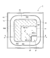
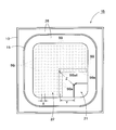
- FIG. 1 is a plan view of a semiconductor device according to a first embodiment of the present invention.
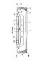
- FIG. 2 is a cross-sectional view taken along line AA in FIG. It is a graph which shows the relationship between the number of short gates, and dv / dt tolerance. It is a top view of the semiconductor device concerning a 2nd embodiment of the present invention. It is a top view of the semiconductor device concerning a 3rd embodiment of the present invention.
- the semiconductor device 1 according to this embodiment is a thyristor.
- the semiconductor device 1 includes a first conductivity type semiconductor substrate 10, a second conductivity type first semiconductor region 11, a first conductivity type second semiconductor region 12, and , A second conductivity type third semiconductor region 13, a second conductivity type fourth semiconductor region 14, a first conductivity type bulk region 17, a gate electrode 21, a first main electrode 22, A second main electrode 23.
- the first conductivity type is N type
- the second conductivity type is P type
- the first main electrode 22 is a cathode electrode
- the second main electrode 23 is an anode electrode.
- the first semiconductor region 11 and the third semiconductor region 13 are also called P-type base regions
- the second semiconductor region 12 is also called an N-type emitter region.
- the first conductivity type may be P-type
- the second conductivity type may be N-type.
- the semiconductor device 1 has a PNPN structure including a third semiconductor region 13, a bulk region 17, a first semiconductor region 11, and a second semiconductor region 12. Yes.
- the first main electrode 22 and the second main electrode are caused to flow through the gate electrode 21 with a reverse bias applied between the first main electrode 22 and the second main electrode 23. 23 is conducted. 2 indicate the boundaries of the depletion layer formed in the semiconductor substrate 10 when a reverse bias is applied to the semiconductor device 1.
- the semiconductor substrate 10 has a main surface 10a (first main surface) and a main surface 10b (second main surface) opposite to the main surface 10a.
- the main surface 10 a is the upper surface of the semiconductor substrate 10
- the main surface 10 b is the lower surface of the semiconductor substrate 10.
- the semiconductor substrate 10 is, for example, a silicon substrate, but may be other semiconductor substrates (SiC substrate, GaN substrate, etc.).
- the semiconductor substrate 10 is N-type in this embodiment, but may be a P-type semiconductor substrate.
- the first semiconductor region 11 is formed on the main surface 10 a of the semiconductor substrate 10.
- the impurity concentration of the first semiconductor region 11 is, for example, 1 ⁇ 10 17 cm ⁇ 3 to 1 ⁇ 10 19 cm ⁇ 3 .
- the thickness of the first semiconductor region 11 is 40 ⁇ m, for example.
- the second semiconductor region 12 is formed in the first semiconductor region 11.
- the impurity concentration of the second semiconductor region 12 is, for example, 1 ⁇ 10 19 cm ⁇ 3 to 1 ⁇ 10 20 cm ⁇ 3 .
- the thickness of the second semiconductor region 12 is, for example, 20 ⁇ m.
- the third semiconductor region 13 is formed on the main surface 10 b of the semiconductor substrate 10.
- the impurity concentration of the third semiconductor region 13 is, for example, 1 ⁇ 10 18 cm ⁇ 3 to 1 ⁇ 10 20 cm ⁇ 3 .
- the thickness of the third semiconductor region 13 is, for example, 30 ⁇ m to 40 ⁇ m.
- the fourth semiconductor region 14 is formed in the first semiconductor region 11.
- the fourth semiconductor region 14 is a region (P + region) having a higher concentration than the first semiconductor region 11.
- the impurity concentration of the fourth semiconductor region 14 is, for example, 1 ⁇ 10 19 cm ⁇ 3 to 1 ⁇ 10 20 cm ⁇ 3 .
- the thickness of the fourth semiconductor region 14 is, for example, 10 ⁇ m.
- the bulk region 17 is a region other than the diffusion regions (the first to fourth semiconductor regions 11 to 14, the isolation region 16, etc.) among the regions in the semiconductor substrate 10.
- the impurity concentration of the bulk region 17 is, for example, 1 ⁇ 10 13 cm ⁇ 3 to 1 ⁇ 10 16 cm ⁇ 3 .
- the thickness of the bulk region 17 is, for example, 120 ⁇ m.
- the second semiconductor region 12 is provided with a plurality of short gates (a first short gate SG1 and a second short gate SG2 described later) penetrating the second semiconductor region 12.
- a first short gate SG1 and a second short gate SG2 described later By providing the short gate, when a steep voltage is applied between the first main electrode 22 and the second main electrode 23, the current charged in the junction capacitance in the semiconductor substrate 10 passes through the short gate through the first gate electrode.
- the semiconductor device 1 can maintain the off state because the main electrode 22 is removed.
- the diameter of the short gate is, for example, 0.1 mm or less.
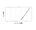
- FIG. 3 is a graph showing the result of simulating the relationship between the number of short gates and the dv / dt tolerance.
- the short gates are evenly arranged.
- the dv / dt resistance of the semiconductor device 1 is improved almost in proportion to the number of short gates.
- the dv / dt tolerance of the semiconductor device 1 may not be proportional to the number of short gates.
- the gate electrode 21 is formed on the main surface 10 a so as to be electrically connected to the first semiconductor region 11. More specifically, the gate electrode 21 is formed on the fourth semiconductor region 14 so as to make ohmic contact.
- the first main electrode 22 is formed on the main surface 10a so as to be electrically connected to the second semiconductor region 12, as shown in FIG. More specifically, the first main electrode 22 is formed on the second semiconductor region 12 so as to make ohmic contact. As shown in FIG. 1, the first main electrode 22 and the gate electrode 21 are formed in a substantially square shape with rounded corners, with the gate electrode 21 occupying one corner in plan view. The first main electrode 22 and the gate electrode 21 are not limited to a substantially square shape, and may be formed in a substantially rectangular shape.
- the second main electrode 23 is formed on the main surface 10b so as to be electrically connected to the third semiconductor region 13 as shown in FIG. More specifically, the second main electrode 23 is formed on the third semiconductor region 13 so as to make ohmic contact.
- the semiconductor device 1 further includes a first conductivity type channel stopper 15, a second conductivity type isolation region 16 provided at an end of the semiconductor device 1, and a protective film 25 that protects the upper surface of the semiconductor device 1. I have.
- the channel stopper 15 is formed in an annular shape so as to surround the gate electrode 21 and the main electrode 22 in a plan view of the semiconductor device 1.
- the channel stopper 15 is a higher concentration region (N + region) than the bulk region 17.
- the impurity concentration of the channel stopper 15 is, for example, 1 ⁇ 10 19 cm ⁇ 3 to 1 ⁇ 10 20 cm ⁇ 3 .
- the isolation region 16 is a region (P + region) having a higher concentration than the third semiconductor region 13.
- the protective film 25 is made of, for example, a silicon oxide film.
- the first main electrode 22 includes a first electrode region A1 adjacent to the gate electrode 21 in a plane parallel to the main surface 10a (that is, when the semiconductor device 1 is viewed in plan), And a second electrode region A2 located on the opposite side of the gate electrode 21 across the first electrode region A1.
- first electrode region A1 a plurality of first conductivity type first short gates SG1 are provided.
- second electrode region A2 a plurality of second conductivity type second short gates SG2 are provided.
- the first short gate SG1 and the second short gate SG2 both penetrate the second semiconductor region 12 and are connected to the first main electrode 22 and the first semiconductor region 11. It is configured as follows.
- the first short gate SG1 and the plurality of second short gates SG2 have the same composition as the first semiconductor region 11, and a part of the first semiconductor region 11 penetrates the second semiconductor region. It can also be considered that the first main electrode 22 has been reached.
- the first electrode region A1 is a region close to the gate electrode 21, the first short gate SG1 has a relatively large influence on the on-characteristics of the semiconductor device 1.
- the second electrode region A2 is a region far from the gate electrode 21, the second short gate SG2 hardly affects the ON characteristics of the semiconductor device 1.
- the nearest short gate SG1a has a great influence on the on characteristics of the semiconductor device 1.
- the nearest short gate SG1a is a short gate located in the foremost column when viewed from the gate electrode 21 among the plurality of first short gates SG1. In FIG. 1, there are three nearest short gates SG1a.
- the submerged resistance r is a resistance component in the first semiconductor region 11 below the second semiconductor region 12 sandwiched between the fourth semiconductor region 14 and the nearest short gate SG1a. is there.
- the shortest gate that is farthest from the gate electrode 21 is called a trigger short gate SG1at. Since the distance between the trigger short gate SG1at and the gate electrode 21 is the longest among the nearest short gates SG1a, the latent resistance r is the largest. For this reason, when a gate current is allowed to flow through the gate electrode 21, the current starts to flow first between the gate electrode 21 and the trigger short gate SG1at. From this, it can be said that the trigger short gate SG1at is a short gate that has the greatest influence on the on-characteristics of the semiconductor device 1. In the present embodiment, as shown in FIG. 1, the trigger short gate SG ⁇ b> 1 at is located on the diagonal line of the first main electrode 22.
- the distance Z between the trigger short gate SG1at and the gate electrode 21 is set within a distance range based on the reference value.
- the distance Z is the shortest distance between the trigger short gate SG1at and the gate electrode 21, as shown in FIG.
- the reference value is, for example, a specification value of the semiconductor device 1.
- the distance Z is set within the distance range based on the reference value, it is possible to prevent the ON characteristic (gate trigger current) of the semiconductor device 1 from changing greatly. From the viewpoint of on-characteristics, it is preferable to arrange the trigger short gate SG1at at the same position as the conventional semiconductor device.
- the arrangement density of the second short gates SG2 is higher than the arrangement density of the first short gates SG1.
- the second short gate SG2 is provided in the second electrode region A2 so that the arrangement density is higher than that of the first short gate SG1.
- the number of short gates provided on the first main electrode 22 (the sum of the first short gate SG1 and the second short gate SG2) is increased as compared with the conventional semiconductor device, and thus the dv / dt resistance is increased. be able to.
- the distance Z between the trigger short gate SG1at and the gate electrode 21 is set within the distance range based on the reference value, and the arrangement density of the second short gate SG2 is set. Is higher than the arrangement density of the first short gates SG1. Therefore, according to the first embodiment, it is possible to increase the dv / dt resistance without greatly affecting the on-characteristics. As a result, it is possible to reduce dv / dt countermeasure components such as resistors and capacitors that have been conventionally provided between the anode electrode and the cathode electrode in order to cope with a steep voltage. Moreover, since the malfunction of the semiconductor device 1 is prevented by improving the dv / dt tolerance, it is possible to prevent a short circuit failure of a product (regulator, inverter, etc.) to which the semiconductor device 1 is applied.
- the distances between the nearest short gate SG1a and the gate electrode 21 may be within the distance range based on the reference value.
- the distance between the two nearest short gates SG1a other than the trigger short gate SG1at may be within the distance range based on the reference value.
- the ON characteristic (gate trigger current) of the semiconductor device 1 is all arranged at the same position as the conventional semiconductor device.
- the trigger short gate SG1at is preferably arranged at the same position as the conventional semiconductor device, and all the nearest short gates SG1a are arranged at the same position as the conventional semiconductor device. More preferred.
- the arrangement density of the second short gates SG2 may be increased as the distance from the gate electrode 21 increases. Since the short gate farther from the gate electrode 21 has a smaller influence on the on-characteristic of the semiconductor device, the dv / dt resistance can be further improved by effectively suppressing the influence on the on-characteristic. Can do.
- the first short gate SG1 and the second short gate SG2 are arranged on a diagonal line connecting the trigger short gate SG1at and the gate electrode 21 with the shortest distance, and on a line parallel to the diagonal line. You may make it do. Thereby, since the 1st short gate SG1 and the 2nd short gate SG2 are not arrange
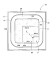
- a semiconductor device 1A according to a second embodiment of the present invention will be described with reference to FIG.
- the difference from the first embodiment is that the size of the short gate SG2 changes according to the distance from the gate electrode 21 in the second embodiment.
- the second embodiment will be described with a focus on differences from the first embodiment.
- the distance Z between the trigger short gate SG1at and the gate electrode 21 is set within a distance range based on the reference value. ing. Therefore, it is possible to prevent the ON characteristic (gate trigger current) of the semiconductor device 1A from changing greatly.
- the size of the trigger short gate SG1at is set to a size based on the reference value. For example, the size of the trigger short gate SG1at is the same as that of the conventional semiconductor device so that the value of the dive resistance r does not change.
- the size of the second short gate SG2 is larger than that of the first short gate SG1.
- the total area of the short gates provided in the first main electrode 22 (the total area of the first short gate SG1 and the second short gate SG2) is increased as compared with the conventional semiconductor device, and therefore the dv / dt resistance. Can be increased.
- the second embodiment it is possible to provide a semiconductor device capable of increasing the dv / dt resistance without greatly affecting the on-characteristics.
- all the distances between the nearest short gate SG1a and the gate electrode 21 may be within the distance range based on the reference value.
- the distance between the two nearest short gates SG1a other than the trigger short gate SG1at may be within the distance range based on the reference value.
- the size of the second short gate SG ⁇ b> 2 may increase as the distance from the gate electrode 21 increases. Since the short gate farther from the gate electrode 21 has a smaller influence on the on-characteristic of the semiconductor device, the dv / dt resistance can be further improved by effectively suppressing the influence on the on-characteristic. Can do.
- the first short gate SG1 and the second short gate SG2 are arranged on a diagonal line connecting the trigger short gate SG1at and the gate electrode 21 with the shortest distance, and on a line parallel to the diagonal line. You may make it do. Thereby, since the 1st short gate SG1 and the 2nd short gate SG2 are not arrange
- a semiconductor device 1B according to a third embodiment of the present invention will be described with reference to FIG.
- the difference from the first embodiment is that in the third embodiment, the first electrode region A1 and the second electrode region A2 are not distinguished, and all the short gates are arranged equally.
- the third embodiment will be described with a focus on differences from the first embodiment.
- a plurality of second conductivity type short gates SG are evenly arranged. Similar to the first short gate SG1 and the second short gate SG2, the plurality of short gates SG are provided so as to penetrate the second semiconductor region 12, and the first main electrode 22 and the first semiconductor region are provided. 11 is connected.
- the plurality of short gates SG are arranged in a square lattice shape, but may be arranged in other shapes such as a rectangular lattice shape, an oblique lattice shape, and a hexagonal lattice shape.
- a plurality of nearest short gates SGa are arranged in the foremost row when viewed from the gate electrode 21.
- 17 nearest short gates SGa are arranged.
- the trigger short gate SGat is the nearest short gate that is farthest from the gate electrode 21.
- the distance Z between the trigger short gate SGat and the gate electrode 21 is within the distance range based on the reference value.
- the reference value is, for example, a specification value of the semiconductor device 1. Thereby, it is possible to prevent the ON characteristic (gate trigger current) of the semiconductor device 1B from changing greatly.
- the distance X between the short gates SG is shorter than the distance Y between the nearest short gate SGa and the gate electrode 21.
- the distance X is the distance between the centers of the adjacent short gates SG
- the distance Y is the shortest distance between the nearest short gate SGa and the gate electrode 21.
- the short gates SG are arranged at a high density, and the number of short gates SG provided in the first main electrode 22 is larger than that in the conventional semiconductor device, so that the dv / dt resistance can be increased. it can.
- the distance between the short gates SG is preferably from 0.1 mm to 0.8 mm, and more preferably from 0.1 mm to 0.5 mm.
- the third embodiment it is possible to provide a semiconductor device capable of increasing the dv / dt resistance without greatly affecting the on-characteristics.
- all the distances between the nearest short gate SGa and the gate electrode 21 may be within the distance range based on the reference value.
- the 16 nearest short gates SGa other than the trigger short gate SGat may also be within the distance range based on the reference value with respect to the gate electrode 21. Thereby, it is possible to further prevent the ON characteristic (gate trigger current) of the semiconductor device 1B from changing greatly.
- the present invention can also be applied to other semiconductor devices such as bidirectional thyristors.
Landscapes
- Thyristors (AREA)
- Electrodes Of Semiconductors (AREA)
Abstract
【課題】半導体装置のオン特性に大きな影響を与えることなく、dv/dt耐量を増加させる。 【解決手段】半導体装置1では、主面10aに平行な平面において、主電極22は、ゲート電極21と隣り合う電極領域A1と、電極領域A1を挟んでゲート電極21の反対側に位置する電極領域A2と、を有し、電極領域A1には複数のショートゲートSG1が設けられ、電極領域A2には複数のショートゲートSG2が設けられており、トリガショートゲートSG1atとゲート電極21との間の距離Zが基準値に基づく距離範囲内にあり、かつ第2のショートゲートSG2の配置密度が第1のショートゲートSG1の配置密度よりも高い。
Description
本発明は、半導体装置に関し、より詳しくは、ゲート電極に電流を流すことによりアノード電極とカソード電極間を導通させる半導体装置に関する。
従来、サイリスタの一種として、矩形状の半導体領域のコーナー部にゲート電極が形成されたコーナーゲート型サイリスタが知られている(特許文献1参照)。
サイリスタの特性の一つにdv/dt耐量がある。dv/dt耐量はサイリスタの誤動作のし易さを表しており、この値が小さいとサイリスタが誤ってオンするおそれがある。dv/dt耐量を増加させるために、特許文献1に記載のサイリスタのように、P型ベース領域内に形成されたN型エミッタ領域を貫通するP型半導体領域(以下、本願では「ショートゲート」(Short Gate:SG)という。)が設けられる。ショートゲートはN型エミッタ領域と並列に設けられた抵抗である。
上記ショートゲートを設けることにより、逆バイアスが印加された半導体装置内の接合容量を充電する電流(充電電流)がショートゲートを通ってカソード電極に流れるようになる。このため、N型エミッタ領域からP型ベース領域への電子の注入量が減少し、急峻な電圧が印加されてもサイリスタはオフ状態を維持することができるようになる。この結果、dv/dt耐量が向上する。
しかしながら、dv/dt耐量とゲートトリガ電流(IGT)とは正の相関関係にある。このため、ショートゲートの数を増やしてdv/dt耐量を大きくした場合、ゲートトリガ電流(IGT)も大きくなる(すなわち、オン特性が大きく変化する)という課題があった。
そこで、本発明は、オン特性に大きな影響を与えることなく、dv/dt耐量を増加させることが可能な半導体装置を提供することを目的とする。
本発明に係る半導体装置は、
第1の主面、および前記第1の主面の反対側の第2の主面を有する第1導電型の半導体基板と、
前記半導体基板の前記第1の主面に形成された第2導電型の第1の半導体領域と、
前記第1半導体領域内に形成された第1導電型の第2の半導体領域と、
前記半導体基板の前記第2の主面に形成された第2導電型の第3の半導体領域と、
前記第1の半導体領域に電気的に接続するように前記第1の主面上に形成されたゲート電極と、
前記第2の半導体領域に電気的に接続するように前記第1の主面上に形成された第1の主電極と、
前記第3の半導体領域に電気的に接続するように前記第2の主面上に形成された第2の主電極と、を備え、
前記第1の主面に平行な平面において、前記第1の主電極は、前記ゲート電極と隣り合う第1の電極領域と、前記第1の電極領域を挟んで前記ゲート電極の反対側に位置する第2の電極領域と、を有しており、
前記第1の電極領域には、前記第2の半導体領域を貫通し且つ前記第1の主電極および前記第1の半導体領域に接続する第2導電型の複数の第1のショートゲートが設けられ、
前記第2の電極領域には、前記第2の半導体領域を貫通し且つ前記第1の主電極および前記第1の半導体領域に接続する第2導電型の複数の第2のショートゲートが設けられ、
前記複数の第1のショートゲートのうち前記ゲート電極から見て最前列に位置する最近傍ショートゲートであって前記ゲート電極から最も離れているトリガショートゲートと、前記ゲート電極との間の距離は、基準値に基づく距離範囲内にあり、かつ
前記第2のショートゲートの配置密度は、前記第1のショートゲートの配置密度よりも高いことを特徴とする。
第1の主面、および前記第1の主面の反対側の第2の主面を有する第1導電型の半導体基板と、
前記半導体基板の前記第1の主面に形成された第2導電型の第1の半導体領域と、
前記第1半導体領域内に形成された第1導電型の第2の半導体領域と、
前記半導体基板の前記第2の主面に形成された第2導電型の第3の半導体領域と、
前記第1の半導体領域に電気的に接続するように前記第1の主面上に形成されたゲート電極と、
前記第2の半導体領域に電気的に接続するように前記第1の主面上に形成された第1の主電極と、
前記第3の半導体領域に電気的に接続するように前記第2の主面上に形成された第2の主電極と、を備え、
前記第1の主面に平行な平面において、前記第1の主電極は、前記ゲート電極と隣り合う第1の電極領域と、前記第1の電極領域を挟んで前記ゲート電極の反対側に位置する第2の電極領域と、を有しており、
前記第1の電極領域には、前記第2の半導体領域を貫通し且つ前記第1の主電極および前記第1の半導体領域に接続する第2導電型の複数の第1のショートゲートが設けられ、
前記第2の電極領域には、前記第2の半導体領域を貫通し且つ前記第1の主電極および前記第1の半導体領域に接続する第2導電型の複数の第2のショートゲートが設けられ、
前記複数の第1のショートゲートのうち前記ゲート電極から見て最前列に位置する最近傍ショートゲートであって前記ゲート電極から最も離れているトリガショートゲートと、前記ゲート電極との間の距離は、基準値に基づく距離範囲内にあり、かつ
前記第2のショートゲートの配置密度は、前記第1のショートゲートの配置密度よりも高いことを特徴とする。
また、前記半導体装置において、
前記最近傍ショートゲートと前記ゲート電極との間の距離は全て、前記基準値に基づく距離範囲内にあるようにしてもよい。
前記最近傍ショートゲートと前記ゲート電極との間の距離は全て、前記基準値に基づく距離範囲内にあるようにしてもよい。
また、前記半導体装置において、
前記第2のショートゲートの配置密度は、前記ゲート電極から遠ざかるほど高くなるようにしてもよい。
前記第2のショートゲートの配置密度は、前記ゲート電極から遠ざかるほど高くなるようにしてもよい。
また、前記半導体装置において、
前記第1の主電極と前記ゲート電極は、平面視して前記ゲート電極が一隅を占める略正方形状に形成されており、
前記第1のショートゲートおよび前記第2のショートゲートは、前記トリガショートゲートと前記ゲート電極とを最短距離で結ぶ対角線、および前記対角線に平行な線に配置されているようにしてもよい。
前記第1の主電極と前記ゲート電極は、平面視して前記ゲート電極が一隅を占める略正方形状に形成されており、
前記第1のショートゲートおよび前記第2のショートゲートは、前記トリガショートゲートと前記ゲート電極とを最短距離で結ぶ対角線、および前記対角線に平行な線に配置されているようにしてもよい。
本発明の半導体装置は、
第1の主面、および前記第1の主面の反対側の第2の主面を有する第1導電型の半導体基板と、
前記半導体基板の前記第1の主面に形成された第2導電型の第1の半導体領域と、
前記第1半導体領域内に形成された第1導電型の第2の半導体領域と、
前記半導体基板の前記第2の主面に形成された第2導電型の第3の半導体領域と、
前記第1の半導体領域に電気的に接続するように前記第1の主面上に形成されたゲート電極と、
前記第2の半導体領域に電気的に接続するように前記第1の主面上に形成された第1の主電極と、
前記第3の半導体領域に電気的に接続するように前記第2の主面上に形成された第2の主電極と、を備え、
前記第1の主面に平行な平面において、前記第1の主電極は、前記ゲート電極と隣り合う第1の電極領域と、前記第1の電極領域を挟んで前記ゲート電極の反対側に位置する第2の電極領域と、を有しており、
前記第1の電極領域には、前記第2の半導体領域を貫通し且つ前記第1の主電極および前記第1の半導体領域に接続する第2導電型の複数の第1のショートゲートが設けられ、
前記第2の電極領域には、前記第2の半導体領域を貫通し且つ前記第1の主電極および前記第1の半導体領域に接続する第2導電型の複数の第2のショートゲートが設けられ、
前記複数の第1のショートゲートのうち前記ゲート電極から見て最前列に位置する最近傍ショートゲートであって前記ゲート電極から最も離れているトリガショートゲートと、前記ゲート電極との間の距離は、基準値に基づく距離範囲内にあり、かつ
前記第2のショートゲートの大きさは、前記第1のショートゲートよりも大きいことを特徴とする。
第1の主面、および前記第1の主面の反対側の第2の主面を有する第1導電型の半導体基板と、
前記半導体基板の前記第1の主面に形成された第2導電型の第1の半導体領域と、
前記第1半導体領域内に形成された第1導電型の第2の半導体領域と、
前記半導体基板の前記第2の主面に形成された第2導電型の第3の半導体領域と、
前記第1の半導体領域に電気的に接続するように前記第1の主面上に形成されたゲート電極と、
前記第2の半導体領域に電気的に接続するように前記第1の主面上に形成された第1の主電極と、
前記第3の半導体領域に電気的に接続するように前記第2の主面上に形成された第2の主電極と、を備え、
前記第1の主面に平行な平面において、前記第1の主電極は、前記ゲート電極と隣り合う第1の電極領域と、前記第1の電極領域を挟んで前記ゲート電極の反対側に位置する第2の電極領域と、を有しており、
前記第1の電極領域には、前記第2の半導体領域を貫通し且つ前記第1の主電極および前記第1の半導体領域に接続する第2導電型の複数の第1のショートゲートが設けられ、
前記第2の電極領域には、前記第2の半導体領域を貫通し且つ前記第1の主電極および前記第1の半導体領域に接続する第2導電型の複数の第2のショートゲートが設けられ、
前記複数の第1のショートゲートのうち前記ゲート電極から見て最前列に位置する最近傍ショートゲートであって前記ゲート電極から最も離れているトリガショートゲートと、前記ゲート電極との間の距離は、基準値に基づく距離範囲内にあり、かつ
前記第2のショートゲートの大きさは、前記第1のショートゲートよりも大きいことを特徴とする。
また、前記半導体装置において、
前記最近傍ショートゲートと前記ゲート電極との間の距離は全て、前記基準値に基づく距離範囲内にあるようにしてもよい。
前記最近傍ショートゲートと前記ゲート電極との間の距離は全て、前記基準値に基づく距離範囲内にあるようにしてもよい。
また、前記半導体装置において、
前記第2のショートゲートの大きさは、前記ゲート電極から遠ざかるほど大きくなるようにしてもよい。
前記第2のショートゲートの大きさは、前記ゲート電極から遠ざかるほど大きくなるようにしてもよい。
また、前記半導体装置において、
前記第1の主電極と前記ゲート電極は、平面視して前記ゲート電極が一隅を占める略正方形状に形成されており、
前記第1のショートゲートおよび前記第2のショートゲートは、前記トリガショートゲートと前記ゲート電極とを最短距離で結ぶ対角線、および前記対角線に平行な線に配置されているようにしてもよい。
前記第1の主電極と前記ゲート電極は、平面視して前記ゲート電極が一隅を占める略正方形状に形成されており、
前記第1のショートゲートおよび前記第2のショートゲートは、前記トリガショートゲートと前記ゲート電極とを最短距離で結ぶ対角線、および前記対角線に平行な線に配置されているようにしてもよい。
本発明に係る半導体装置は、
第1の主面、および前記第1の主面の反対側の第2の主面を有する第1導電型の半導体基板と、
前記半導体基板の前記第1の主面に形成された第2導電型の第1の半導体領域と、
前記第1半導体領域内に形成された第1導電型の第2の半導体領域と、
前記半導体基板の前記第2の主面に形成された第2導電型の第3の半導体領域と、
前記第1の半導体領域に電気的に接続するように前記第1の主面上に形成されたゲート電極と、
前記第2の半導体領域に電気的に接続するように前記第1の主面上に形成された第1の主電極と、
前記第3の半導体領域に電気的に接続するように前記第2の主面上に形成された第2の主電極と、
前記第2の半導体領域を貫通するように設けられ、前記第1の主電極および前記第1の半導体領域に接続する第2導電型の複数のショートゲートと、を備え、
前記複数のショートゲートのうち前記ゲート電極から見て最前列に位置する最近傍ショートゲートであって前記ゲート電極から最も離れているトリガショートゲートと、前記ゲート電極との間の距離は、基準値に基づく距離範囲内にあり、
前記ショートゲート同士間の距離は、前記最近傍ショートゲートと前記ゲート電極との間の最短距離よりも短いことを特徴とする。
第1の主面、および前記第1の主面の反対側の第2の主面を有する第1導電型の半導体基板と、
前記半導体基板の前記第1の主面に形成された第2導電型の第1の半導体領域と、
前記第1半導体領域内に形成された第1導電型の第2の半導体領域と、
前記半導体基板の前記第2の主面に形成された第2導電型の第3の半導体領域と、
前記第1の半導体領域に電気的に接続するように前記第1の主面上に形成されたゲート電極と、
前記第2の半導体領域に電気的に接続するように前記第1の主面上に形成された第1の主電極と、
前記第3の半導体領域に電気的に接続するように前記第2の主面上に形成された第2の主電極と、
前記第2の半導体領域を貫通するように設けられ、前記第1の主電極および前記第1の半導体領域に接続する第2導電型の複数のショートゲートと、を備え、
前記複数のショートゲートのうち前記ゲート電極から見て最前列に位置する最近傍ショートゲートであって前記ゲート電極から最も離れているトリガショートゲートと、前記ゲート電極との間の距離は、基準値に基づく距離範囲内にあり、
前記ショートゲート同士間の距離は、前記最近傍ショートゲートと前記ゲート電極との間の最短距離よりも短いことを特徴とする。
また、前記半導体装置において、
前記最近傍ショートゲートと前記ゲート電極との間の距離は全て、前記基準値に基づく距離範囲内にあるようにしてもよい。
前記最近傍ショートゲートと前記ゲート電極との間の距離は全て、前記基準値に基づく距離範囲内にあるようにしてもよい。
また、前記半導体装置において、
前記ショートゲート同士間の距離は、0.1mm以上0.8mm以下であるようにしてもよい。
前記ショートゲート同士間の距離は、0.1mm以上0.8mm以下であるようにしてもよい。
また、前記半導体装置において、
前記ショートゲート同士間の距離は、0.1mm以上0.5mm以下であるようにしてもよい。
前記ショートゲート同士間の距離は、0.1mm以上0.5mm以下であるようにしてもよい。
また、前記半導体装置において、
前記複数のショートゲートは、均等に配置されているようにしてもよい。
前記複数のショートゲートは、均等に配置されているようにしてもよい。
本発明によれば、オン特性に大きな影響を与えることなく、dv/dt耐量を増加させることが可能な半導体装置を提供することができる。
以下、図面を参照しつつ本発明の実施形態に係る半導体装置について説明する。なお、各図において同等の機能を有する構成要素には同一の符号を付し、同一符号の構成要素の詳しい説明は繰り返さない。
(第1の実施形態)
本発明の第1の実施形態に係る半導体装置について、図1および図2を参照して説明する。本実施形態に係る半導体装置1はサイリスタである。
本発明の第1の実施形態に係る半導体装置について、図1および図2を参照して説明する。本実施形態に係る半導体装置1はサイリスタである。
半導体装置1は、図1および図2に示すように、第1導電型の半導体基板10と、第2導電型の第1の半導体領域11と、第1導電型の第2の半導体領域12と、第2導電型の第3の半導体領域13と、第2導電型の第4の半導体領域14と、第1導電型のバルク領域17と、ゲート電極21と、第1の主電極22と、第2の主電極23と、を備えている。
本実施形態において、第1導電型はN型であり、第2導電型はP型である。第1の主電極22がカソード電極であり、第2の主電極23がアノード電極である。第1の半導体領域11および第3の半導体領域13はP型ベース領域とも呼ばれ、第2の半導体領域12はN型エミッタ領域とも呼ばれる。なお、第1導電型がP型であり、第2導電型がN型であってもよい。
半導体装置1では、図2に示すように、第3の半導体領域13、バルク領域17、第1の半導体領域11および第2の半導体領域12からなるP-N-P-N構造を有している。
半導体装置1では、第1の主電極22と第2の主電極23間に逆バイアスが印加された状態でゲート電極21にゲート電流を流すことにより第1の主電極22と第2の主電極23間が導通する。図2の境界線D1,D2は、半導体装置1に逆バイアスが印加された時に半導体基板10内に形成される空乏層の境界を示している。
次に、半導体装置1の各構成要素について詳しく説明する。
半導体基板10は、図2に示すように、主面10a(第1の主面)、および主面10aの反対側の主面10b(第2の主面)を有する。図2では、主面10aは半導体基板10の上面であり、主面10bは半導体基板10の下面である。半導体基板10は、例えばシリコン基板であるが、その他の半導体基板(SiC基板、GaN基板等)であってもよい。なお、半導体基板10は、本実施形態ではN型であるが、P型の半導体基板であってもよい。
図2に示すように、第1の半導体領域11は、半導体基板10の主面10aに形成されている。第1の半導体領域11の不純物濃度は、例えば1×1017cm-3~1×1019cm-3である。第1の半導体領域11の厚みは、例えば40μmである。
第2の半導体領域12は、第1の半導体領域11内に形成されている。第2の半導体領域12の不純物濃度は、例えば1×1019cm-3~1×1020cm-3である。第2の半導体領域12の厚みは、例えば20μmである。
第3の半導体領域13は、半導体基板10の主面10bに形成されている。第3の半導体領域13の不純物濃度は、例えば1×1018cm-3~1×1020cm-3である。第3の半導体領域13の厚みは、例えば30μm~40μmである。
第4の半導体領域14は、第1の半導体領域11内に形成されている。第4の半導体領域14は、第1の半導体領域11よりも高濃度の領域(P+領域)である。第4の半導体領域14の不純物濃度は、例えば1×1019cm-3~1×1020cm-3である。第4の半導体領域14の厚みは、例えば10μmである。
バルク領域17は、半導体基板10内の領域のうち拡散領域(第1~第4の半導体領域11~14、アイソレーション領域16等)以外の領域である。バルク領域17の不純物濃度は、例えば1×1013cm-3~1×1016cm-3である。バルク領域17の厚みは、例えば120μmである。
第2の半導体領域12には、第2の半導体領域12を貫通する複数のショートゲート(後述の第1のショートゲートSG1および第2のショートゲートSG2)が設けられている。ショートゲートを設けることで、第1の主電極22と第2の主電極23間に急峻な電圧が印加される際、半導体基板10内の接合容量に充電される電流がショートゲートを通って第1の主電極22に抜けるため、半導体装置1はオフ状態を維持することができる。なお、ショートゲートの直径は、例えば0.1mm以下である。
ここで、ショートゲートの個数がdv/dt耐量に与える影響について説明する。図3は、ショートゲートの個数とdv/dt耐量との関係をシミュレーションした結果を示すグラフである。ここでは、ショートゲートは均等に配置されている。図3から分かるように、半導体装置1のdv/dt耐量はショートゲートの個数にほぼ比例して向上する。ただし、ショートゲートが過度に不均等に配置される場合、半導体装置1のdv/dt耐量はショートゲートの個数に比例しないことがある。
ゲート電極21は、図2に示すように、第1の半導体領域11に電気的に接続するように主面10a上に形成されている。より詳しくは、ゲート電極21は、オーミック接触するように第4の半導体領域14上に形成されている。
第1の主電極22は、図2に示すように、第2の半導体領域12に電気的に接続するように主面10a上に形成されている。より詳しくは、第1の主電極22は、オーミック接触するように第2の半導体領域12上に形成されている。第1の主電極22とゲート電極21は、図1に示すように、平面視してゲート電極21が一隅を占める、角が丸められた略正方形状に形成されている。なお、略正方形状に限らず、第1の主電極22とゲート電極21は略長方形状に形成されてもよい。
第2の主電極23は、図2に示すように、第3の半導体領域13に電気的に接続するように主面10b上に形成されている。より詳しくは、第2の主電極23は、オーミック接触するように第3の半導体領域13上に形成されている。
半導体装置1は、第1導電型のチャネルストッパー15と、半導体装置1の端部に設けられた第2導電型のアイソレーション領域16と、半導体装置1の上面を保護する保護膜25とをさらに備えている。
チャネルストッパー15は、図1に示すように、半導体装置1を平面視してゲート電極21および主電極22を囲うように環状に形成されている。このチャネルストッパー15は、バルク領域17よりも高濃度の領域(N+領域)である。チャネルストッパー15の不純物濃度は、例えば1×1019cm-3~1×1020cm-3である。アイソレーション領域16は、第3の半導体領域13よりも高濃度の領域(P+領域)である。保護膜25は、例えばシリコン酸化膜からなる。
次に、第1の実施形態に係る半導体装置1に設けられたショートゲートについて詳しく説明する。
図1に示すように、第1の主電極22は、主面10aに平行な平面において(すなわち、半導体装置1を平面視した際)、ゲート電極21と隣り合う第1の電極領域A1と、この第1の電極領域A1を挟んでゲート電極21の反対側に位置する第2の電極領域A2と、を有している。
第1の電極領域A1には、第2導電型の複数の第1のショートゲートSG1が設けられている。第2の電極領域A2には、第2導電型の複数の第2のショートゲートSG2が設けられている。
図2に示すように、第1のショートゲートSG1および第2のショートゲートSG2はいずれも、第2の半導体領域12を貫通し且つ第1の主電極22および第1の半導体領域11に接続するように構成されている。第1のショートゲートSG1および複数の第2のショートゲートSG2は、第1の半導体領域11と同じ組成を有しており、第1の半導体領域11の一部が第2の半導体領域を貫通して第1の主電極22まで到達しているものと捉えることも可能である。
第1の電極領域A1はゲート電極21に近い領域であるため、第1のショートゲートSG1は半導体装置1のオン特性に比較的大きな影響を与える。一方、第2の電極領域A2はゲート電極21から遠い領域であるため、第2のショートゲートSG2は半導体装置1のオン特性にほとんど影響を与えない。
第1のショートゲートSG1のなかでも最近傍ショートゲートSG1aは半導体装置1のオン特性に対して大きな影響を与える。この最近傍ショートゲートSG1aは、複数の第1のショートゲートSG1のうちゲート電極21から見て最前列に位置するショートゲートのことである。図1では、3本の最近傍ショートゲートSG1aが存在する。
最近傍ショートゲートSG1aとゲート電極21間の距離が短くなるにつれて潜り抵抗rが小さくなるため、ゲートトリガ電流は大きくなる。反対に、最近傍ショートゲートSG1aとゲート電極21間の距離が長くなるにつれて潜り抵抗rが大きくなるため、ゲートトリガ電流は小さくなる。なお、潜り抵抗rは、図2に示すように、第4の半導体領域14と最近傍ショートゲートSG1aに挟まれた第2の半導体領域12下方の第1の半導体領域11における抵抗成分のことである。
最近傍ショートゲートSG1aのうちゲート電極21から最も離れているショートゲートをトリガショートゲートSG1atと呼ぶことにする。トリガショートゲートSG1atとゲート電極21間の距離は最近傍ショートゲートSG1aの中で最も長いため、潜り抵抗rが最も大きい。このため、ゲート電極21にゲート電流を流していくと、ゲート電極21とトリガショートゲートSG1at間に最初に電流が流れ始める。このことから、トリガショートゲートSG1atは、半導体装置1のオン特性に最も大きな影響を与えるショートゲートであると言える。本実施形態では、図1に示すように、トリガショートゲートSG1atは、第1の主電極22の対角線上に位置する。
トリガショートゲートSG1atとゲート電極21との間の距離Zは、基準値に基づく距離範囲内に設定されている。ここで、距離Zは、図1に示すように、トリガショートゲートSG1atとゲート電極21との間の最短距離である。上記の基準値は、例えば、半導体装置1の仕様値である。このように距離Zが基準値に基づく距離範囲内に設定されていることにより、半導体装置1のオン特性(ゲートトリガ電流)が大きく変化することが防止される。オン特性の観点からは、トリガショートゲートSG1atを従来の半導体装置と同じ位置に配置することが好ましい。
半導体装置1では、図1に示すように、第2のショートゲートSG2の配置密度は、第1のショートゲートSG1の配置密度よりも高い。換言すれば、第2のショートゲートSG2は、第1のショートゲートSG1よりも配置密度が高くなるように第2の電極領域A2に設けられている。これにより、第1の主電極22に設けられるショートゲートの個数(第1のショートゲートSG1と第2のショートゲートSG2の和)が従来の半導体装置よりも増えるため、dv/dt耐量を増加させることができる。
上記のように、第1の実施形態では、トリガショートゲートSG1atとゲート電極21との間の距離Zが基準値に基づく距離範囲内に設定されており、かつ第2のショートゲートSG2の配置密度が第1のショートゲートSG1の配置密度よりも高い。よって、第1の実施形態によれば、オン特性に大きな影響を与えることなく、dv/dt耐量を増加させることができる。その結果、急峻な電圧に対応するために従来アノード電極とカソード電極間に設けられていた、抵抗やコンデンサ等のdv/dt対策部品を削減することができる。また、dv/dt耐量が向上することにより半導体装置1の誤動作が防止されるため、半導体装置1の適用製品(レギュレータ、インバータ等)の短絡故障を防止することができる。
なお、最近傍ショートゲートSG1aとゲート電極21との間の距離は全て、基準値に基づく距離範囲内にあるようにしてもよい。図1の場合では、トリガショートゲートSG1at以外の2本の最近傍ショートゲートSG1aについても、ゲート電極21との間の距離が基準値に基づく距離範囲内にあるようにしてもよい。これにより、半導体装置1のオン特性(ゲートトリガ電流)が大きく変化することをさらに防止できる。例えば、最近傍ショートゲートSG1aについては全て、従来の半導体装置と同じ位置に配置する。このように、オン特性の観点からは、トリガショートゲートSG1atを従来の半導体装置と同じ位置に配置することが好ましく、全ての最近傍ショートゲートSG1aを従来の半導体装置と同じ位置に配置することがより好ましい。
また、第2のショートゲートSG2の配置密度は、ゲート電極21から遠ざかるほど高くなるようにしてもよい。ゲート電極21から遠いショートゲートほど半導体装置のオン特性に与える影響が小さくなることから、このようにすることで、オン特性への影響を効果的に抑えつつ、dv/dt耐量をより向上させることができる。
また、図1に示すように、第1のショートゲートSG1および第2のショートゲートSG2は、トリガショートゲートSG1atとゲート電極21とを最短距離で結ぶ対角線、および当該対角線に平行な線に配置されるようにしてもよい。これにより、第1のショートゲートSG1および第2のショートゲートSG2が過度に不均等に配置されることがないため、dv/dt耐量の増加が抑制されることを防止できる。
(第2の実施形態)
次に、本発明の第2の実施形態に係る半導体装置1Aについて、図4を参照して説明する。第1の実施形態との相違点は、第2の実施形態では、ショートゲートSG2の大きさがゲート電極21からの距離に応じて変化する点である。以下、第1の実施形態との相違点を中心に第2の実施形態について説明する。
次に、本発明の第2の実施形態に係る半導体装置1Aについて、図4を参照して説明する。第1の実施形態との相違点は、第2の実施形態では、ショートゲートSG2の大きさがゲート電極21からの距離に応じて変化する点である。以下、第1の実施形態との相違点を中心に第2の実施形態について説明する。
本実施形態に係る半導体装置1Aでは、第1の実施形態で説明した半導体装置1と同様に、トリガショートゲートSG1atとゲート電極21との間の距離Zは基準値に基づく距離範囲内に設定されている。したがって、半導体装置1Aのオン特性(ゲートトリガ電流)が大きく変化することを防止できる。なお、トリガショートゲートSG1atの大きさは、基準値に基づく大きさに設定されている。例えば、潜り抵抗rの値が変化しないように、トリガショートゲートSG1atの大きさは従来の半導体装置と同じ大きさとする。
図4に示すように、第2の実施形態では、第2のショートゲートSG2の大きさは、第1のショートゲートSG1よりも大きい。これにより、第1の主電極22に設けられるショートゲートの総面積(第1のショートゲートSG1と第2のショートゲートSG2の面積の総和)が従来の半導体装置よりも増えるため、dv/dt耐量を増加させることができる。
よって、第2の実施形態によれば、オン特性に大きな影響を与えることなく、dv/dt耐量を増加させることが可能な半導体装置を提供することができる。
なお、最近傍ショートゲートSG1aとゲート電極21との間の距離は全て、基準値に基づく距離範囲内にあるようにしてもよい。図4の場合では、トリガショートゲートSG1at以外の2本の最近傍ショートゲートSG1aについても、ゲート電極21との間の距離が基準値に基づく距離範囲内にあるようにしてもよい。これにより、半導体装置1Aのオン特性(ゲートトリガ電流)が大きく変化することをさらに防止できる。
また、図4に示すように、第2のショートゲートSG2の大きさは、ゲート電極21から遠ざかるほど大きくなるようにしてもよい。ゲート電極21から遠いショートゲートほど半導体装置のオン特性に与える影響が小さくなることから、このようにすることで、オン特性への影響を効果的に抑えつつ、dv/dt耐量をより向上させることができる。
また、図4に示すように、第1のショートゲートSG1および第2のショートゲートSG2は、トリガショートゲートSG1atとゲート電極21とを最短距離で結ぶ対角線、および当該対角線に平行な線に配置されるようにしてもよい。これにより、第1のショートゲートSG1および第2のショートゲートSG2が過度に不均等に配置されることがないため、dv/dt耐量の増加が抑制されることを防止できる。
(第3の実施形態)
次に、本発明の第3の実施形態に係る半導体装置1Bについて、図5を参照して説明する。第1の実施形態との相違点は、第3の実施形態では、第1の電極領域A1と第2の電極領域A2の区別をせず、全てのショートゲートが均等に配置される点である。以下、第1の実施形態との相違点を中心に第3の実施形態について説明する。
次に、本発明の第3の実施形態に係る半導体装置1Bについて、図5を参照して説明する。第1の実施形態との相違点は、第3の実施形態では、第1の電極領域A1と第2の電極領域A2の区別をせず、全てのショートゲートが均等に配置される点である。以下、第1の実施形態との相違点を中心に第3の実施形態について説明する。
本実施形態に係る半導体装置1Bでは、図5に示すように、第2導電型の複数のショートゲートSGが均等に配置されている。複数のショートゲートSGは、第1のショートゲートSG1および第2のショートゲートSG2と同様に、第2の半導体領域12を貫通するように設けられ、第1の主電極22および第1の半導体領域11に接続するように構成されている。なお、図5では、複数のショートゲートSGは、正方格子状に配置されているが矩形格子状、斜方格子状、六角格子状など他の配置態様であってもよい。
図5に示すように、複数のショートゲートSGのうちゲート電極21から見て最前列に、複数の最近傍ショートゲートSGaが配置されている。図5の例では、17本の最近傍ショートゲートSGaが配置されている。トリガショートゲートSGatは、ゲート電極21から最も離れている最近傍ショートゲートである。
トリガショートゲートSGatとゲート電極21との間の距離Zは、基準値に基づく距離範囲内にある。上記の基準値は、例えば、半導体装置1の仕様値である。これにより、半導体装置1Bのオン特性(ゲートトリガ電流)が大きく変化することを防止できる。
また、図5に示すように、ショートゲートSG同士間の距離Xは、最近傍ショートゲートSGaとゲート電極21との間の距離Yよりも短い。ここで、距離Xは、隣り合うショートゲートSGの中心間距離であり、距離Yは、最近傍ショートゲートSGaとゲート電極21との間の最短距離である。このように半導体装置1BではショートゲートSGが高密度に配置され、第1の主電極22に設けられるショートゲートSGの個数が従来の半導体装置よりも増えるため、dv/dt耐量を増加させることができる。なお、ショートゲートSG同士間の距離は0.1mm以上0.8mm以下であることが好ましく、0.1mm以上0.5mm以下であることがさらに好ましい。
よって、第3の実施形態によれば、オン特性に大きな影響を与えることなく、dv/dt耐量を増加させることが可能な半導体装置を提供することができる。
なお、最近傍ショートゲートSGaとゲート電極21との間の距離は全て、基準値に基づく距離範囲内にあるようにしてもよい。図5の場合では、トリガショートゲートSGat以外の16本の最近傍ショートゲートSGaについても、ゲート電極21との間の距離が基準値に基づく距離範囲内にあるようにしてもよい。これにより、半導体装置1Bのオン特性(ゲートトリガ電流)が大きく変化することをさらに防止できる。
以上、本発明に係る3つの実施形態について説明したが、本発明は、双方向サイリスタ等の他の半導体装置にも適用可能である。
上記の記載に基づいて、当業者であれば、本発明の追加の効果や種々の変形を想到できるかもしれないが、本発明の態様は、上述した個々の実施形態に限定されるものではない。異なる実施形態にわたる構成要素を適宜組み合わせてもよい。特許請求の範囲に規定された内容及びその均等物から導き出される本発明の概念的な思想と趣旨を逸脱しない範囲で種々の追加、変更及び部分的削除が可能である。
1,1A,1B 半導体装置
10 半導体基板
10a,10b 主面
11 第1の半導体領域(P型ベース領域)
12 第2の半導体領域(N型エミッタ領域)
13 第3の半導体領域(P型ベース領域)
14 第4の半導体領域
15 チャネルストッパー
16 アイソレーション領域
17 バルク領域
21 ゲート電極
22 第1の主電極(カソード電極)
23 第2の主電極(アノード電極)
25 保護膜
A1 第1の電極領域
A2 第2の電極領域
D1,D2 (空乏層の)境界線
r 潜り抵抗
SG,SG1,SG2 ショートゲート
SG1a 最近傍ショートゲート
SG1at トリガショートゲート
X,Y,Z 距離
10 半導体基板
10a,10b 主面
11 第1の半導体領域(P型ベース領域)
12 第2の半導体領域(N型エミッタ領域)
13 第3の半導体領域(P型ベース領域)
14 第4の半導体領域
15 チャネルストッパー
16 アイソレーション領域
17 バルク領域
21 ゲート電極
22 第1の主電極(カソード電極)
23 第2の主電極(アノード電極)
25 保護膜
A1 第1の電極領域
A2 第2の電極領域
D1,D2 (空乏層の)境界線
r 潜り抵抗
SG,SG1,SG2 ショートゲート
SG1a 最近傍ショートゲート
SG1at トリガショートゲート
X,Y,Z 距離
Claims (13)
- 第1の主面、および前記第1の主面の反対側の第2の主面を有する第1導電型の半導体基板と、
前記半導体基板の前記第1の主面に形成された第2導電型の第1の半導体領域と、
前記第1半導体領域内に形成された第1導電型の第2の半導体領域と、
前記半導体基板の前記第2の主面に形成された第2導電型の第3の半導体領域と、
前記第1の半導体領域に電気的に接続するように前記第1の主面上に形成されたゲート電極と、
前記第2の半導体領域に電気的に接続するように前記第1の主面上に形成された第1の主電極と、
前記第3の半導体領域に電気的に接続するように前記第2の主面上に形成された第2の主電極と、を備え、
前記第1の主面に平行な平面において、前記第1の主電極は、前記ゲート電極と隣り合う第1の電極領域と、前記第1の電極領域を挟んで前記ゲート電極の反対側に位置する第2の電極領域と、を有しており、
前記第1の電極領域には、前記第2の半導体領域を貫通し且つ前記第1の主電極および前記第1の半導体領域に接続する第2導電型の複数の第1のショートゲートが設けられ、
前記第2の電極領域には、前記第2の半導体領域を貫通し且つ前記第1の主電極および前記第1の半導体領域に接続する第2導電型の複数の第2のショートゲートが設けられ、
前記複数の第1のショートゲートのうち前記ゲート電極から見て最前列に位置する最近傍ショートゲートであって前記ゲート電極から最も離れているトリガショートゲートと、前記ゲート電極との間の距離は、基準値に基づく距離範囲内にあり、かつ
前記第2のショートゲートの配置密度は、前記第1のショートゲートの配置密度よりも高いことを特徴とする半導体装置。 - 前記最近傍ショートゲートと前記ゲート電極との間の距離は全て、前記基準値に基づく距離範囲内にあることを特徴とする請求項1に記載の半導体装置。
- 前記第2のショートゲートの配置密度は、前記ゲート電極から遠ざかるほど高くなることを特徴とする請求項1に記載の半導体装置。
- 前記第1の主電極と前記ゲート電極は、平面視して前記ゲート電極が一隅を占める略正方形状に形成されており、
前記第1のショートゲートおよび前記第2のショートゲートは、前記トリガショートゲートと前記ゲート電極とを最短距離で結ぶ対角線、および前記対角線に平行な線に配置されていることを特徴とする請求項1に記載の半導体装置。 - 第1の主面、および前記第1の主面の反対側の第2の主面を有する第1導電型の半導体基板と、
前記半導体基板の前記第1の主面に形成された第2導電型の第1の半導体領域と、
前記第1半導体領域内に形成された第1導電型の第2の半導体領域と、
前記半導体基板の前記第2の主面に形成された第2導電型の第3の半導体領域と、
前記第1の半導体領域に電気的に接続するように前記第1の主面上に形成されたゲート電極と、
前記第2の半導体領域に電気的に接続するように前記第1の主面上に形成された第1の主電極と、
前記第3の半導体領域に電気的に接続するように前記第2の主面上に形成された第2の主電極と、を備え、
前記第1の主面に平行な平面において、前記第1の主電極は、前記ゲート電極と隣り合う第1の電極領域と、前記第1の電極領域を挟んで前記ゲート電極の反対側に位置する第2の電極領域と、を有しており、
前記第1の電極領域には、前記第2の半導体領域を貫通し且つ前記第1の主電極および前記第1の半導体領域に接続する第2導電型の複数の第1のショートゲートが設けられ、
前記第2の電極領域には、前記第2の半導体領域を貫通し且つ前記第1の主電極および前記第1の半導体領域に接続する第2導電型の複数の第2のショートゲートが設けられ、
前記複数の第1のショートゲートのうち前記ゲート電極から見て最前列に位置する最近傍ショートゲートであって前記ゲート電極から最も離れているトリガショートゲートと、前記ゲート電極との間の距離は、基準値に基づく距離範囲内にあり、かつ
前記第2のショートゲートの大きさは、前記第1のショートゲートよりも大きいことを特徴とする半導体装置。 - 前記最近傍ショートゲートと前記ゲート電極との間の距離は全て、前記基準値に基づく距離範囲内にあることを特徴とする請求項5に記載の半導体装置。
- 前記第2のショートゲートの大きさは、前記ゲート電極から遠ざかるほど大きくなることを特徴とする請求項5に記載の半導体装置。
- 前記第1の主電極と前記ゲート電極は、平面視して前記ゲート電極が一隅を占める略正方形状に形成されており、
前記第1のショートゲートおよび前記第2のショートゲートは、前記トリガショートゲートと前記ゲート電極とを最短距離で結ぶ対角線、および前記対角線に平行な線に配置されていることを特徴とする請求項5に記載の半導体装置。 - 第1の主面、および前記第1の主面の反対側の第2の主面を有する第1導電型の半導体基板と、
前記半導体基板の前記第1の主面に形成された第2導電型の第1の半導体領域と、
前記第1半導体領域内に形成された第1導電型の第2の半導体領域と、
前記半導体基板の前記第2の主面に形成された第2導電型の第3の半導体領域と、
前記第1の半導体領域に電気的に接続するように前記第1の主面上に形成されたゲート電極と、
前記第2の半導体領域に電気的に接続するように前記第1の主面上に形成された第1の主電極と、
前記第3の半導体領域に電気的に接続するように前記第2の主面上に形成された第2の主電極と、
前記第2の半導体領域を貫通するように設けられ、前記第1の主電極および前記第1の半導体領域に接続する第2導電型の複数のショートゲートと、を備え、
前記複数のショートゲートのうち前記ゲート電極から見て最前列に位置する最近傍ショートゲートであって前記ゲート電極から最も離れているトリガショートゲートと、前記ゲート電極との間の距離は、基準値に基づく距離範囲内にあり、
前記ショートゲート同士間の距離は、前記最近傍ショートゲートと前記ゲート電極との間の最短距離よりも短いことを特徴とする半導体装置。 - 前記最近傍ショートゲートと前記ゲート電極との間の距離は全て、前記基準値に基づく距離範囲内にあることを特徴とする請求項9に記載の半導体装置。
- 前記ショートゲート同士間の距離は、0.1mm以上0.8mm以下であることを特徴とする請求項9に記載の半導体装置。
- 前記ショートゲート同士間の距離は、0.1mm以上0.5mm以下であることを特徴とする請求項9に記載の半導体装置。
- 前記複数のショートゲートは、均等に配置されていることを特徴とする請求項9に記載の半導体装置。
Priority Applications (2)
| Application Number | Priority Date | Filing Date | Title |
|---|---|---|---|
| JP2017542492A JP6371011B1 (ja) | 2017-03-15 | 2017-03-15 | 半導体装置 |
| PCT/JP2017/010389 WO2018167871A1 (ja) | 2017-03-15 | 2017-03-15 | 半導体装置 |
Applications Claiming Priority (1)
| Application Number | Priority Date | Filing Date | Title |
|---|---|---|---|
| PCT/JP2017/010389 WO2018167871A1 (ja) | 2017-03-15 | 2017-03-15 | 半導体装置 |
Publications (1)
| Publication Number | Publication Date |
|---|---|
| WO2018167871A1 true WO2018167871A1 (ja) | 2018-09-20 |
Family
ID=63104425
Family Applications (1)
| Application Number | Title | Priority Date | Filing Date |
|---|---|---|---|
| PCT/JP2017/010389 Ceased WO2018167871A1 (ja) | 2017-03-15 | 2017-03-15 | 半導体装置 |
Country Status (2)
| Country | Link |
|---|---|
| JP (1) | JP6371011B1 (ja) |
| WO (1) | WO2018167871A1 (ja) |
Cited By (1)
| Publication number | Priority date | Publication date | Assignee | Title |
|---|---|---|---|---|
| WO2023053945A1 (ja) * | 2021-09-29 | 2023-04-06 | 新電元工業株式会社 | 双方向サイリスタ |
Citations (3)
| Publication number | Priority date | Publication date | Assignee | Title |
|---|---|---|---|---|
| JPS6088469A (ja) * | 1983-10-20 | 1985-05-18 | Fuji Electric Co Ltd | サイリスタ |
| US20050082565A1 (en) * | 2003-10-17 | 2005-04-21 | Stmicroelectronics S.A. | Isolated HF-control SCR switch |
| JP2009206193A (ja) * | 2008-02-26 | 2009-09-10 | Sansha Electric Mfg Co Ltd | トライアック |
Family Cites Families (2)
| Publication number | Priority date | Publication date | Assignee | Title |
|---|---|---|---|---|
| JPS51112191A (en) * | 1975-03-18 | 1976-10-04 | Hitachi Ltd | Thyristor |
| JPH07335862A (ja) * | 1994-06-09 | 1995-12-22 | Hitachi Ltd | 半導体装置及びその製造方法 |
-
2017
- 2017-03-15 WO PCT/JP2017/010389 patent/WO2018167871A1/ja not_active Ceased
- 2017-03-15 JP JP2017542492A patent/JP6371011B1/ja active Active
Patent Citations (3)
| Publication number | Priority date | Publication date | Assignee | Title |
|---|---|---|---|---|
| JPS6088469A (ja) * | 1983-10-20 | 1985-05-18 | Fuji Electric Co Ltd | サイリスタ |
| US20050082565A1 (en) * | 2003-10-17 | 2005-04-21 | Stmicroelectronics S.A. | Isolated HF-control SCR switch |
| JP2009206193A (ja) * | 2008-02-26 | 2009-09-10 | Sansha Electric Mfg Co Ltd | トライアック |
Cited By (5)
| Publication number | Priority date | Publication date | Assignee | Title |
|---|---|---|---|---|
| WO2023053945A1 (ja) * | 2021-09-29 | 2023-04-06 | 新電元工業株式会社 | 双方向サイリスタ |
| CN116195071A (zh) * | 2021-09-29 | 2023-05-30 | 新电元工业株式会社 | 双向晶闸管 |
| TWI830403B (zh) * | 2021-09-29 | 2024-01-21 | 日商新電元工業股份有限公司 | 雙向閘流體 |
| EP4411826A4 (en) * | 2021-09-29 | 2025-01-01 | Shindengen Electric Manufacturing Co., Ltd. | Bidirectional thyristor |
| US12527017B2 (en) | 2021-09-29 | 2026-01-13 | Shindengen Electric Manufacturing Co., Ltd. | Bidirectional thyristor |
Also Published As
| Publication number | Publication date |
|---|---|
| JPWO2018167871A1 (ja) | 2019-03-28 |
| JP6371011B1 (ja) | 2018-08-08 |
Similar Documents
| Publication | Publication Date | Title |
|---|---|---|
| US10784256B2 (en) | Semiconductor device and method of manufacturing semiconductor device | |
| CN106463540B (zh) | 半导体装置 | |
| JP5340018B2 (ja) | 半導体装置 | |
| US10700054B2 (en) | Semiconductor apparatus | |
| JP2013152996A (ja) | 半導体装置 | |
| US7772669B2 (en) | Semiconductor device having an improved structure for high withstand voltage | |
| CN102544002A (zh) | 半导体装置及其制造方法 | |
| JP2015176927A (ja) | 半導体装置および絶縁ゲート型バイポーラトランジスタ | |
| CN109360825B (zh) | 双向开关 | |
| JP6619522B1 (ja) | ワイドギャップ半導体装置 | |
| TW201630148A (zh) | 靜電放電保護器件 | |
| US12512667B2 (en) | Asymmetric bidirectional surge protection device | |
| US20180240792A1 (en) | Semiconductor device | |
| JP6371011B1 (ja) | 半導体装置 | |
| TW202401827A (zh) | 半導體裝置 | |
| JP6718140B2 (ja) | 半導体装置 | |
| TWI477018B (zh) | 暫態電壓抑制器電路與用於其中之二極體元件及其製造方法 | |
| JP2016162898A (ja) | 半導体装置 | |
| US20190280109A1 (en) | Semiconductor device | |
| JP2009146977A (ja) | 半導体装置 | |
| JP7263978B2 (ja) | 半導体装置 | |
| JP2014165317A (ja) | 半導体装置 | |
| US20110193099A1 (en) | Semiconductor device | |
| CN111095565B (zh) | 半导体装置 | |
| US11784220B2 (en) | Semiconductor device |
Legal Events
| Date | Code | Title | Description |
|---|---|---|---|
| ENP | Entry into the national phase |
Ref document number: 2017542492 Country of ref document: JP Kind code of ref document: A |
|
| 121 | Ep: the epo has been informed by wipo that ep was designated in this application |
Ref document number: 17901081 Country of ref document: EP Kind code of ref document: A1 |
|
| NENP | Non-entry into the national phase |
Ref country code: DE |
|
| 122 | Ep: pct application non-entry in european phase |
Ref document number: 17901081 Country of ref document: EP Kind code of ref document: A1 |