WO2018163386A1 - 基板処理装置、半導体装置の製造方法およびプログラム - Google Patents
基板処理装置、半導体装置の製造方法およびプログラム Download PDFInfo
- Publication number
- WO2018163386A1 WO2018163386A1 PCT/JP2017/009610 JP2017009610W WO2018163386A1 WO 2018163386 A1 WO2018163386 A1 WO 2018163386A1 JP 2017009610 W JP2017009610 W JP 2017009610W WO 2018163386 A1 WO2018163386 A1 WO 2018163386A1
- Authority
- WO
- WIPO (PCT)
- Prior art keywords
- microwave
- substrate
- wafer
- temperature
- film
- Prior art date
- Legal status (The legal status is an assumption and is not a legal conclusion. Google has not performed a legal analysis and makes no representation as to the accuracy of the status listed.)
- Ceased
Links
Images











Classifications
-
- H—ELECTRICITY
- H10—SEMICONDUCTOR DEVICES; ELECTRIC SOLID-STATE DEVICES NOT OTHERWISE PROVIDED FOR
- H10P—GENERIC PROCESSES OR APPARATUS FOR THE MANUFACTURE OR TREATMENT OF DEVICES COVERED BY CLASS H10
- H10P72/00—Handling or holding of wafers, substrates or devices during manufacture or treatment thereof
- H10P72/04—Apparatus for manufacture or treatment
- H10P72/0431—Apparatus for thermal treatment
-
- H—ELECTRICITY
- H10—SEMICONDUCTOR DEVICES; ELECTRIC SOLID-STATE DEVICES NOT OTHERWISE PROVIDED FOR
- H10P—GENERIC PROCESSES OR APPARATUS FOR THE MANUFACTURE OR TREATMENT OF DEVICES COVERED BY CLASS H10
- H10P72/00—Handling or holding of wafers, substrates or devices during manufacture or treatment thereof
- H10P72/04—Apparatus for manufacture or treatment
- H10P72/0431—Apparatus for thermal treatment
- H10P72/0436—Apparatus for thermal treatment mainly by radiation
-
- H—ELECTRICITY
- H01—ELECTRIC ELEMENTS
- H01J—ELECTRIC DISCHARGE TUBES OR DISCHARGE LAMPS
- H01J37/00—Discharge tubes with provision for introducing objects or material to be exposed to the discharge, e.g. for the purpose of examination or processing thereof
- H01J37/32—Gas-filled discharge tubes
- H01J37/32009—Arrangements for generation of plasma specially adapted for examination or treatment of objects, e.g. plasma sources
- H01J37/32192—Microwave generated discharge
-
- H—ELECTRICITY
- H05—ELECTRIC TECHNIQUES NOT OTHERWISE PROVIDED FOR
- H05B—ELECTRIC HEATING; ELECTRIC LIGHT SOURCES NOT OTHERWISE PROVIDED FOR; CIRCUIT ARRANGEMENTS FOR ELECTRIC LIGHT SOURCES, IN GENERAL
- H05B6/00—Heating by electric, magnetic or electromagnetic fields
- H05B6/64—Heating using microwaves
- H05B6/66—Circuits
- H05B6/68—Circuits for monitoring or control
-
- H—ELECTRICITY
- H05—ELECTRIC TECHNIQUES NOT OTHERWISE PROVIDED FOR
- H05B—ELECTRIC HEATING; ELECTRIC LIGHT SOURCES NOT OTHERWISE PROVIDED FOR; CIRCUIT ARRANGEMENTS FOR ELECTRIC LIGHT SOURCES, IN GENERAL
- H05B6/00—Heating by electric, magnetic or electromagnetic fields
- H05B6/64—Heating using microwaves
- H05B6/80—Apparatus for specific applications
- H05B6/806—Apparatus for specific applications for laboratory use
-
- H—ELECTRICITY
- H10—SEMICONDUCTOR DEVICES; ELECTRIC SOLID-STATE DEVICES NOT OTHERWISE PROVIDED FOR
- H10P—GENERIC PROCESSES OR APPARATUS FOR THE MANUFACTURE OR TREATMENT OF DEVICES COVERED BY CLASS H10
- H10P34/00—Irradiation with electromagnetic or particle radiation of wafers, substrates or parts of devices
- H10P34/40—Irradiation with electromagnetic or particle radiation of wafers, substrates or parts of devices with high-energy radiation
- H10P34/42—Irradiation with electromagnetic or particle radiation of wafers, substrates or parts of devices with high-energy radiation with electromagnetic radiation, e.g. laser annealing
-
- H—ELECTRICITY
- H10—SEMICONDUCTOR DEVICES; ELECTRIC SOLID-STATE DEVICES NOT OTHERWISE PROVIDED FOR
- H10P—GENERIC PROCESSES OR APPARATUS FOR THE MANUFACTURE OR TREATMENT OF DEVICES COVERED BY CLASS H10
- H10P72/00—Handling or holding of wafers, substrates or devices during manufacture or treatment thereof
- H10P72/06—Apparatus for monitoring, sorting, marking, testing or measuring
- H10P72/0602—Temperature monitoring
-
- H—ELECTRICITY
- H10—SEMICONDUCTOR DEVICES; ELECTRIC SOLID-STATE DEVICES NOT OTHERWISE PROVIDED FOR
- H10P—GENERIC PROCESSES OR APPARATUS FOR THE MANUFACTURE OR TREATMENT OF DEVICES COVERED BY CLASS H10
- H10P72/00—Handling or holding of wafers, substrates or devices during manufacture or treatment thereof
- H10P72/06—Apparatus for monitoring, sorting, marking, testing or measuring
- H10P72/0612—Production flow monitoring, e.g. for increasing throughput
-
- H—ELECTRICITY
- H10—SEMICONDUCTOR DEVICES; ELECTRIC SOLID-STATE DEVICES NOT OTHERWISE PROVIDED FOR
- H10P—GENERIC PROCESSES OR APPARATUS FOR THE MANUFACTURE OR TREATMENT OF DEVICES COVERED BY CLASS H10
- H10P95/00—Generic processes or apparatus for manufacture or treatments not covered by the other groups of this subclass
- H10P95/90—Thermal treatments, e.g. annealing or sintering
Definitions
- the present invention relates to a substrate processing apparatus, a semiconductor device manufacturing method, and a program.
- a substrate in a processing chamber is heated using a heating device to change a composition or a crystal structure in a thin film formed on the surface of the substrate.
- a modification process typified by an annealing process for repairing crystal defects or the like in the formed thin film.
- miniaturization and high integration have been remarkable in semiconductor devices, and accordingly, a modification process to a high-density substrate on which a pattern having a high aspect ratio is formed is required.
- a heat treatment method using microwaves has been studied.
- the substrate In conventional heat treatment using microwaves, the substrate cannot be heated uniformly, and the target film may not be uniformly processed.
- An object of the present invention is to provide a technique that enables uniform substrate processing.
- a heating apparatus having a processing chamber for processing a substrate, a plurality of microwave supply sources for supplying microwaves for heating the substrate in the processing chamber, and the plurality of microwave supplies
- the plurality of microwave supply sources are controlled so that the periods during which the plurality of microwave supply sources are turned off are different while the microwave input power supplied to the substrate from each of the sources is constant.
- a technology is provided that includes a control unit configured.
- a technique capable of performing uniform substrate processing can be provided.
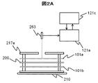
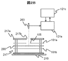
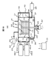
- FIG. 1 It is a schematic block diagram of the single wafer processing furnace of the substrate processing apparatus used suitably by one Embodiment in this invention, and is a figure which shows a processing furnace part with a longitudinal cross-sectional view. It is a figure which shows the temperature measuring method of the substrate processing apparatus used suitably by one Embodiment in this invention, and is a figure at the time of measuring the temperature of a heat insulation board. It is a figure which shows the temperature measuring method of the substrate processing apparatus used suitably by one Embodiment in this invention, and is a figure at the time of measuring the temperature of a board
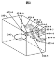
- FIG. 1 it is a figure which shows the structural example of the electromagnetic wave supply part at the time of providing six electromagnetic wave introduction ports in a case.
- FIG. 4 is a top view of the case of FIG. 3. It is a side view of the case of FIG. It is a schematic block diagram of the controller of the substrate processing apparatus used suitably by this invention. It is a figure which shows the flow of the substrate processing in this invention. It is a figure which shows an example of the microwave irradiation method in Example 1 of the substrate processing apparatus used suitably by one Embodiment in this invention, and the temperature transition of a board
- FIG. 1 It is a figure which shows the Hall mobility of the process sample 1 used for one Embodiment in this invention. It is a figure which shows the cross-sectional density
- FIG. 1 It is a schematic block diagram of the vertical batch type processing furnace of the substrate processing apparatus used suitably by other embodiment in this invention, and is a figure which shows a processing furnace part with a longitudinal cross-sectional view. It is a figure which shows the processing furnace part in the modification 1 of the substrate processing apparatus used suitably by other embodiment in this invention with a longitudinal cross-sectional view. It is sectional drawing of the substrate holder in the modification 2 of the substrate processing apparatus used suitably by other embodiment in this invention.
- the substrate processing apparatus 100 is configured as a single wafer heat treatment apparatus that performs various heat treatments on a wafer.
- the substrate processing apparatus 100 will be described as an apparatus that performs an annealing process (modification process) using an electromagnetic wave, which will be described later. (Processing room) As shown in FIG.
- a substrate processing apparatus 100 includes a case 102 as a cavity (upper container) made of a material that reflects electromagnetic waves such as metal, and a case 102 that is accommodated in the case 102 and is vertically It has a cylindrical reaction tube 103 whose upper and lower ends are open.
- the reaction tube 103 is made of a material that transmits electromagnetic waves, such as quartz.
- a cap flange (blocking plate) 104 made of a metal material is brought into contact with the upper end of the reaction tube 103 via an O-ring 220 as a sealing member (seal member) to close the upper end of the reaction tube 103.
- a processing vessel for processing a substrate such as a silicon wafer is mainly constituted by the case 102, the reaction tube 103, and the cap flange 104.
- the inner space of the reaction tube 103 is constituted as a processing chamber 201.
- the processing vessel may be configured by the case 102 and the cap flange 104 without providing the reaction tube 103. In that case, the internal space of the case 102 becomes the processing chamber 201.
- the processing vessel may be configured by the case 102 and the reaction tube 103 or the case 102 using the case 102 whose ceiling is closed without providing the cap flange 104.
- a mounting table 210 is provided below the reaction tube 103, and a boat 217 as a substrate holder for holding a wafer 200 as a substrate is mounted on the upper surface of the mounting table 210.
- the boat 217 holds a wafer 200 to be processed and quartz plates 101 a and 101 b as heat insulating plates placed vertically above and below the wafer 200 so as to sandwich the wafer 200 at a predetermined interval.
- quartz plates 101a and 101b for example, a silicon plate (Si plate) or a silicon carbide plate (SiC plate) is formed of a material such as a dielectric that absorbs electromagnetic waves and heats itself.
- a component having a function as a susceptor (also referred to as a radiation plate or a soaking plate) (not shown) that indirectly heats the plate may be placed.
- the susceptor may be configured to be placed outside the wafer 200 and inside the quartz plate 101a and the quartz plate 101b. That is, the wafer 200 is sandwiched between susceptors, and the susceptor is sandwiched between quartz plates 101a and 101b (so as to be disposed between the wafer 200 and the quartz plate 101a, and between the wafer 200 and the quartz plate 101b). It may be configured. With this configuration, the wafer 200 can be more efficiently and uniformly heated.
- the quartz plates 101a and 101b are the same components, and hereinafter, when there is no need to distinguish between them, the quartz plates 101a and 101b will be referred to as the quartz plate 101.
- a protrusion (not shown) that protrudes in the radial direction of the mounting table 210 is provided on the bottom surface side of the mounting table 210.
- the protruding portion approaches or contacts a squeezing plate 204 provided between the processing chamber 201 and the transfer space 203 described later, the atmosphere in the processing chamber 201 moves into the transfer space 203 or the transfer space 203. The atmosphere inside is prevented from moving into the processing chamber 201.
- the case 102 as the upper container has, for example, a circular cross section and is configured as a flat hermetic container.
- the transport container 202 as a lower container is made of, for example, a metal material such as aluminum (Al) or stainless steel (SUS), or quartz.
- a transfer area 203 for transferring a wafer 200 such as a silicon wafer is formed below the processing container.
- a space surrounded by the case 102 or a space surrounded by the reaction tube 103 and above the partition plate 204 is referred to as a processing chamber 201 or a reaction area 201 serving as a processing space, and is referred to as a transfer container 202.
- the space below the partition plate may be referred to as a transport area 203 as a transport space.
- processing chamber 201 and the transfer area 203 are not limited to be configured to be adjacent to each other in the vertical direction as in the present embodiment, but may be configured to be adjacent to each other in the horizontal direction, or may not be provided with the transfer area 203. It is good also as a structure which has only.
- a substrate loading / unloading port 206 adjacent to the gate valve 205 is provided on the side surface of the transfer container 202, and the wafer 200 moves between a substrate transfer chamber (not shown) via the substrate loading / unloading port 206.
- An electromagnetic wave supply unit as a heating device which will be described in detail later, is installed on the side surface of the case 102.
- An electromagnetic wave such as a microwave supplied from the electromagnetic wave supply unit is introduced into the processing chamber 201 to heat the wafer 200 and the like. Then, the wafer 200 is processed.
- the mounting table 210 is supported by a shaft 255 as a rotating shaft.
- the shaft 255 passes through the bottom of the transport container 202 and is connected to a drive mechanism 267 that rotates and moves up and down outside the transport container 202.
- a drive mechanism 267 that rotates and moves up and down outside the transport container 202.
- the periphery of the lower end portion of the shaft 255 is covered with a bellows 212, and the inside of the processing chamber 201 and the transfer area 203 is kept airtight.
- the mounting table 210 When the wafer 200 is transferred, the mounting table 210 is lowered so that the upper surface of the mounting table is positioned at the substrate loading / unloading port 206 (wafer transfer position), and when the wafer 200 is processed, the wafer 200 is processed as shown in FIG. It moves up to the processing position (wafer processing position) in the chamber 201.
- a mechanism for raising and lowering the mounting table is provided. You may make it provide only the mechanism which rotates a mounting base, without providing.
- An exhaust unit that exhausts the atmosphere of the processing chamber 201 is provided below the processing chamber 201 and on the outer peripheral side of the mounting table 210. As shown in FIG. 1, an exhaust port 221 is provided in the exhaust part. An exhaust pipe 231 is connected to the exhaust port 221, and a pressure regulator 244 such as an APC valve that controls the valve opening degree according to the pressure in the processing chamber 201 and a vacuum pump 246 are connected in series to the exhaust pipe 231. It is connected to the.
- a pressure regulator 244 such as an APC valve that controls the valve opening degree according to the pressure in the processing chamber 201 and a vacuum pump 246 are connected in series to the exhaust pipe 231. It is connected to the.
- the pressure regulator 244 is not limited to an APC valve as long as it can receive pressure information in the processing chamber 201 (a feedback signal from a pressure sensor 245 described later) and adjust the exhaust amount.
- the on-off valve and the pressure regulating valve may be used in combination.
- the exhaust port 221, the exhaust pipe 231, and the pressure regulator 244 mainly constitute an exhaust part (also referred to as an exhaust system or an exhaust line).
- an exhaust port may be provided so as to surround the mounting table 210 so that the gas can be exhausted from the entire circumference of the wafer 200.
- the cap flange 104 is provided with a gas supply pipe 232 for supplying a processing gas for processing various substrates such as an inert gas, a raw material gas, and a reactive gas into the processing chamber 201.
- a mass flow controller (MFC) 241 that is a flow rate controller (flow rate control unit) and a valve 243 that is an on-off valve are provided in order from the upstream side.
- MFC mass flow controller
- N 2 nitrogen
- a gas provided with an MFC as a flow controller and a valve as an on-off valve in order from the upstream direction downstream from the valve 243 of the gas supply pipe 232 A plurality of types of gases can be supplied by using a configuration in which a supply pipe is connected.
- a gas supply pipe provided with an MFC and a valve may be installed for each gas type.
- a gas supply system (gas supply unit) is mainly configured by the gas supply pipe 232, the MFC 241, and the valve 243.
- an inert gas flows through the gas supply system, it is also referred to as an inert gas supply system.
- the inert gas for example, a rare gas such as Ar gas, He gas, Ne gas, or Xe gas can be used in addition to N 2 gas.
- the cap flange 104 is provided with a temperature sensor 263 as a non-contact type temperature measuring device. By adjusting the output of a microwave oscillator 655, which will be described later, based on the temperature information detected by the temperature sensor 263, the substrate is heated, and the substrate temperature has a desired temperature distribution.
- the temperature sensor 263 is configured by a radiation thermometer such as an IR (Infrared Radiation) sensor.
- the temperature sensor 263 is installed so as to measure the surface temperature of the quartz plate 101 a or the surface temperature of the wafer 200.
- the susceptor as the heating element described above When the susceptor as the heating element described above is provided, the surface temperature of the susceptor may be measured.
- the wafer temperature converted by the temperature conversion data described later, that is, the estimated wafer temperature, and the temperature sensor 263 are used. A case where the temperature obtained by directly measuring the temperature of the wafer 200 is meant and a case where both are meant will be described.
- FIGS. 2A and 2B an example of a configuration in the case where the surface temperature of the quartz plate 101a and the wafer 200 is measured using the temperature sensor 263 is shown.
- a measurement hole 217b as a temperature measurement window is provided at a position facing the temperature sensor 263 of the boat top plate 217a so that the ceiling portion (top plate) 217a of the boat 217 does not interfere with temperature measurement.
- the surface temperature of the quartz plate 101a is measured.
- the measurement hole 217 b of the boat 217 and the measurement hole 105 as a measurement window are provided in the quartz plate 101 a to measure the surface temperature of the wafer 200.
- the temperature measurement of the quartz plate 101 and the wafer 200 is performed at a preparatory stage before the substrate processing process is performed, and the transition of the temperature change between the quartz plate 101 and the wafer 200 in the substrate processing process is acquired in advance. Is preferred.
- the temperature conversion data indicating the correlation between the temperature of the quartz plate 101 and the wafer 200 is stored in the storage device 121 c or the external storage device 123 by acquiring the transition of the temperature change between the quartz plate 101 and the wafer 200.
- the temperature of the wafer 200 can be estimated by measuring only the temperature of the quartz plate 101, and based on the estimated temperature of the wafer 200.
- the output of the microwave oscillator 655, that is, the heating device is controlled.
- the means for measuring the temperature of the substrate is not limited to the radiation thermometer described above, and the temperature may be measured using a thermocouple, or the thermocouple and the non-contact thermometer are used in combination. May be.
- a thermocouple it is necessary to place the thermocouple near the wafer 200 and perform temperature measurement. That is, since it is necessary to arrange a thermocouple in the processing chamber 201, the thermocouple itself is heated by a microwave supplied from a microwave oscillator to be described later, so that the temperature cannot be measured accurately. Therefore, it is preferable to use a non-contact type thermometer as the temperature sensor 263.
- the temperature sensor 263 is not limited to being provided on the cap flange 104 but may be provided on the mounting table 210.
- the temperature sensor 263 is not only directly installed on the cap flange 104 or the mounting table 210 but also indirectly measured by reflecting the radiated light from the measurement window provided on the cap flange 104 or the mounting table 210 with a mirror or the like. It may be configured to.
- the number of temperature sensors 263 is not limited to one, and a plurality of temperature sensors may be installed. (Electromagnetic wave supply unit) In FIG. 3, the illustration of the microwave oscillator is omitted to avoid the complexity of the drawing.
- FIG. 3 a structure having six electromagnetic wave supply units will be described as an example.
- the electromagnetic wave introduction ports 653-1 and 653-4, the waveguides 654-1 and 654-4, and the microwave oscillators 655-1 and 655-4 that can be confirmed from the side surface are exemplarily shown. It is shown.
- first introduction port 653-1 As shown in FIGS. 1 to 5, there are six electromagnetic wave introduction ports (first introduction port 653-1, second introduction port 653-2, third introduction port 653-3, fourth, An introduction port 653-4, a fifth introduction port 653-5, and a sixth introduction port 653-6) are provided.
- Each of the first introduction port 653-1 to the sixth introduction port 653-6 has six waveguides for supplying electromagnetic waves into the processing chamber 201 (first waveguide 654-1, second waveguide). 654-2, the third waveguide 654-3, the fourth waveguide 654-4, the fifth waveguide 654-5, and the sixth waveguide 654-6) are connected to each other.
- microwave oscillators serving as heating sources for supplying electromagnetic waves into the processing chamber 201 and heating the other ends of the first waveguide 654-1 to the sixth waveguide 654-6, respectively.
- Oscillator 655-1, second microwave oscillator 655-2, third microwave oscillator 655-3, fourth microwave oscillator 655-4, fifth microwave oscillator 655-5, sixth microwave oscillator 655-6) Is connected.
- the microwave oscillator may be referred to as an electromagnetic wave source (microwave source).
- the fourth microwave oscillator is connected to the other end of each of the fourth waveguide 654-4 and the fifth waveguide 654-5. 655-4 and a fifth microwave oscillator 655-5 are connected.
- the wafer 200 is, in this example, a substantially central portion of the case 102, that is, between the electromagnetic wave introduction ports 653-3 and 653-6 in the side view of FIG. Further, it is arranged at a substantially central portion of the case 102 in the top view of FIG. Thereby, the microwaves supplied from the six electromagnetic wave introduction ports can be irradiated almost evenly on the upper surface, the lower surface, or the entire surface of the wafer 200.
- FIG. 3 shows an example of an electromagnetic wave supply unit provided with six electromagnetic wave introduction ports, but four electromagnetic wave introduction ports may be used.
- the electromagnetic wave introduction ports 653-2 and 653-5, the associated waveguides 654-2 and 654-5, and the microwave oscillators 655-2 and 655-5 are deleted.
- the electromagnetic wave supply unit includes four electromagnetic wave introduction ports 654-1, 654-3, 654-4, 654-6, four waveguides 654-1, 654-3, 654-4, 654-6, and four micro waves. It comprises wave oscillators 655-1, 655-3, 655-4, and 655-6.
- the distances of the four electromagnetic wave introduction ports 654-1, 654-3, 654-4, and 654-6 with respect to the wafer 200 in the case 102 or the processing chamber 201 are substantially equalized. Microwaves from the respective electromagnetic wave introduction ports can be applied to the wafer 200 almost evenly.
- the microwave oscillators 655-1 to 655-6 supply electromagnetic waves such as microwaves to the waveguides 654-1 to 654-6, respectively, and are introduced through the waveguides 654-1 to 654-6. Electromagnetic waves are supplied into the processing chamber 201 from the ports 653-1 to 653-6. For each of the microwave oscillators 655-1 to 655-6, a magnetron, a klystron or the like is used.
- the electromagnetic wave introduction ports 653-1 to 653-6, the waveguides 654-1 to 654-6, and the microwave oscillators 655-1 to 655-6 are not particularly required to be described separately.
- the electromagnetic wave introduction port 653, the waveguide 654, and the microwave oscillator 655 will be described.
- the frequency of the electromagnetic wave generated by the microwave oscillator 655 is preferably controlled to be in the frequency range of 13.56 MHz to 24.125 GHz. More preferably, the frequency is preferably controlled to be 2.45 GHz or 5.8 GHz.
- the frequencies of the microwave oscillators 655-1 to 655-6 may be the same frequency, or may be installed at different frequencies.
- microwave oscillators 655 are described so as to be arranged on the side surface of the case 102.
- the present invention is not limited to this, and one microwave oscillator 655 is provided in Examples 1 and 2 described later. It is only necessary to be provided as described above, and it is only necessary that three or more are provided in Example 3 and Example 4 described later. Further, although the microwave oscillator 655 is provided on one side surface of the case 102, the microwave oscillator 655 may be provided on different side surfaces such as the opposite side surfaces of the case 102.
- an electromagnetic wave supply unit (electromagnetic wave supply apparatus, microwave) as a heating apparatus is constituted by the microwave oscillators 655-1 to 655-6, the waveguides 654-1 to 654-6 and the electromagnetic wave introduction ports 653-1 to 653-6.
- a supply unit also referred to as a microwave supply device).
- a controller 121 (to be described later) is connected to each of the microwave oscillators 655-1 to 655-6.
- a temperature sensor 263 for measuring the temperature of the quartz plate 101 a or 101 b accommodated in the processing chamber 201 or the wafer 200 is connected to the controller 121.
- the temperature sensor 263 measures the temperature of the quartz plate 101 or the wafer 200 by the method described above, and transmits the temperature to the controller 121.
- the controller 121 controls the output of the microwave oscillators 655-1 to 655-6. Control heating.
- the heating control method by the heating device includes a method of controlling the heating of the wafer 200 by controlling a voltage input to the microwave oscillator 655, and a time for turning on the power of the microwave oscillator 655.
- a method of controlling the heating of the wafer 200 by changing the ratio of time to turn off (OFF) can be used.
- the microwave oscillators 655-1 to 655-6 are controlled by the same control signal transmitted from the controller 121.
- the present invention is not limited to this, and the microwave oscillators 655-1 to 655-6 are individually controlled by transmitting individual control signals from the controller 121 to the microwave oscillators 655-1 to 655-6, respectively. May be.
- the controller 121 which is a control unit (control device, control means), includes a CPU (Central Processing Unit) 121a, a RAM (Random Access Memory) 121b, a storage device 121c, and an I / O port 121d. It is configured as a computer.
- the RAM 121b, the storage device 121c, and the I / O port 121d are configured to exchange data with the CPU 121a via the internal bus 121e.
- an input / output device 122 configured as a touch panel or the like is connected to the controller 121.
- the storage device 121c includes, for example, a flash memory, a HDD (Hard Disk Drive), and the like.
- a control program for controlling the operation of the substrate processing apparatus, a process recipe describing the annealing (modification) processing procedure and conditions, and the like are stored in a readable manner.
- the process recipe is a combination of the controller 121 that allows the controller 121 to execute each procedure in the substrate processing process described later and obtain a predetermined result, and functions as a program.
- the process recipe, the control program, and the like are collectively referred to simply as a program.
- the process recipe is also simply called a recipe.
- the RAM 121b is configured as a memory area (work area) in which programs, data, and the like read by the CPU 121a are temporarily stored.
- the I / O port 121d is connected to the above-described MFC 241, valve 243, pressure sensor 245, APC valve 244, vacuum pump 246, temperature sensor 263, drive mechanism 267, microwave oscillator 655, and the like.
- the CPU 121a is configured to read out and execute a control program from the storage device 121c and to read a recipe from the storage device 121c in response to an operation command input from the input / output device 122 or the like.
- the CPU 121a adjusts the flow rate of various gases by the MFC 241, the opening / closing operation of the valve 243, the pressure adjusting operation by the APC valve 244 based on the pressure sensor 245, the start and stop of the vacuum pump 246, and the temperature in accordance with the contents of the read recipe.
- the output adjustment operation of the microwave oscillator 655 based on the sensor 263, the rotation and rotation speed adjustment operation of the mounting table 210 (or the boat 217) by the drive mechanism 267, the raising / lowering operation, and the like are controlled.
- the output adjustment operation of the microwave oscillator 655 based on the temperature sensor 263 includes the output adjustment operation of the microwave oscillator 655 described with reference to FIGS. 9, 10, and 11.
- the controller 121 installs the above-described program stored in an external storage device (for example, a magnetic disk such as a hard disk, an optical disk such as a CD, a magneto-optical disk such as an MO, or a semiconductor memory such as a USB memory) 123 in a computer.
- an external storage device for example, a magnetic disk such as a hard disk, an optical disk such as a CD, a magneto-optical disk such as an MO, or a semiconductor memory such as a USB memory
- the storage device 121c and the external storage device 123 are configured as computer-readable recording media.
- the program stored in the computer-readable recording medium includes a description relating to the control of the output adjustment operation of the microwave oscillator 655 described with reference to FIG. 9, FIG. 10, and FIG. Hereinafter, these are collectively referred to simply as a recording medium.
- the term “recording medium” may include only the storage device 121c alone, may include only the external storage device 123 alone, or may include both of them.
- the program may be provided to the computer using a communication means such as the Internet or a dedicated line without using the external storage device 123.
- wafer when used in the present specification, it may mean the wafer itself or a laminate of the wafer and a predetermined layer or film formed on the surface thereof.
- wafer surface when used in this specification, it may mean the surface of the wafer itself, or may mean the surface of a predetermined layer or the like formed on the wafer.
- the phrase “form a predetermined layer on the wafer” means that the predetermined layer is directly formed on the surface of the wafer itself, a layer formed on the wafer, etc. It may mean that a predetermined layer is formed on the substrate.
- substrate is also synonymous with the term “wafer”.
- the valve opening of the pressure regulator 244 is feedback-controlled based on the pressure information detected by the pressure sensor 245 so that the inside of the processing chamber 201 is set to a predetermined pressure.
- the electromagnetic wave supply unit may be controlled as preliminary heating so as to perform heating to a predetermined temperature (S402).
- S402 a predetermined temperature
- the temperature is raised to a predetermined substrate processing temperature by the electromagnetic wave supply unit, it is preferable to raise the temperature with an output smaller than the output of the reforming step described later so that the wafer 200 is not deformed or damaged.
- inert gas supply step (S403) When the pressure and temperature in the processing chamber 201 are controlled to predetermined values in the furnace pressure / temperature adjustment step S402, the drive mechanism 267 rotates the shaft 255 and rotates the wafer 200 via the boat 217 on the mounting table 210. Let At this time, an inert gas such as nitrogen gas is supplied through the gas supply pipe 232 (S403).
- the pressure in the processing chamber 201 is a predetermined value in the range of 10 Pa to 102000 Pa, and is adjusted to be, for example, 101300 Pa to 101650 Pa.
- the shaft may be rotated during the substrate loading step S401, that is, after the loading of the wafer 200 into the processing chamber 201 is completed.
- this process may be implemented simultaneously with furnace pressure and temperature adjustment process S402 as a furnace pressure adjustment method.
- Modification step (S404) When the inside of the processing chamber 201 is maintained at a predetermined pressure, the microwave oscillator 655 supplies the microwave into the processing chamber 201 through the above-described units. By supplying microwaves into the processing chamber 201, the wafer 200 is heated to a temperature of 100 ° C.
- the substrate processing is performed at a temperature at which the wafer 200 efficiently absorbs microwaves, and the speed of the modification processing can be improved.
- the temperature of the wafer 200 is processed at a temperature lower than 100 ° C. or a temperature higher than 1000 ° C., the surface of the wafer 200 is altered and it becomes difficult to absorb microwaves. In this case, it becomes difficult to heat the wafer 200. For this reason, it is desired to perform substrate processing in the above-described temperature range. In order to maintain such a substrate processing temperature zone, it is preferable to perform a cooling process during the reforming process (annealing process).
- a standing wave is generated in the processing chamber 201, and the wafer 200 (when the susceptor is placed, the susceptor is also the same as the wafer 200), A heated concentration region (hot spot) that is locally heated and a region that is not heated (non-heated region) other than that are generated, and a wafer 200 (when the susceptor is mounted, the susceptor is the same as the wafer 200).
- a hot spot is suppressed from being generated on the wafer 200 by controlling on / off of the power supply of the electromagnetic wave supply unit.
- the microwave oscillator 655 By controlling the microwave oscillator 655 as described above, the wafer 200 is heated, and the amorphous silicon film formed on the surface of the wafer 200 is modified (crystallized) into a polysilicon film. That is, the wafer 200 can be uniformly modified.
- the microwave oscillator 655 When the measured temperature of the wafer 200 is higher or lower than the above threshold, the microwave oscillator 655 is not turned off, but the output of the microwave oscillator 655 is controlled so as to be lowered.
- the temperature may be within a predetermined range. In this case, when the temperature of the wafer 200 returns to a temperature within a predetermined range, the output of the microwave oscillator 655 is controlled to be increased.
- the wafer 200 is modified.
- the output (POWER) of the microwave oscillator 655 means the input power of the microwave irradiated in the case 102 or the processing chamber 201.
- the output of the microwave oscillator 655 is a plurality of microwave oscillators. It means the total output of each microwave irradiated from 655-1 to 655-6.
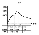
- Example 1 The microwave irradiation method in the furnace pressure / temperature adjustment step S402 and the reforming step S404 in Example 1 will be described with reference to FIG.
- the vertical axis represents temperature (T ° C.), and the horizontal axis represents time (second: sec).
- a preliminary heating process that is a temperature adjustment process, and an annealing process and a cooling process that are reforming processes are sequentially performed.
- the output of the microwave oscillator 655 is set to 4 kW, and the microwaves are irradiated to the wafer 200 in the processing chamber 201 for 180 seconds.
- the output of the microwave oscillator 655 is set to 10 kW, and the wafer 200 in the processing chamber 201 is irradiated with the microwave for 60 seconds.
- the output of the microwave oscillator 655 is set to 0 W, and the temperature of the wafer 200 is cooled.
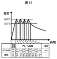
- Example 2 a microwave irradiation method in the furnace pressure / temperature adjustment step S402 and the reforming step S404 in Example 2 will be described with reference to FIG.
- the microwave irradiation method in the second embodiment is different from that in the first embodiment in that, in the annealing process of the reforming process, the microwave irradiation and the microwave are performed so that the processing temperature of the wafer 200 rises and falls within a certain temperature range. This is a point that alternately repeats the stop of irradiation. The other points are the same as in Example 1 unless otherwise specified.
- the vertical axis represents temperature (T ° C.), and the horizontal axis represents time (second: sec).
- a preheating process, an annealing process, and a cooling process are sequentially performed as a temperature adjustment process and a reforming process.
- the preheating process irradiates the wafer in the processing chamber 201 with microwaves for 180 seconds, for example, by setting the output of the microwave oscillator 655 to 4 kW, similarly to the preheating process shown in FIG. Thereby, the temperature of the wafer 200 is raised to about 550 ° C.
- the output of the microwave oscillator 655 is set to 10 kW, and the microwaves are irradiated to the wafer 200 in the processing chamber 201 for 15 seconds. Thereby, the temperature of the wafer 200 is raised to about 680 ° C. Thereafter, the output of the microwave oscillator 655 is set to 0 W for 35 seconds, and the irradiation of the microwave on the wafer 200 is stopped. As a result, the wafer temperature is lowered to a predetermined temperature of about 550 ° C.
- the microwave irradiation to the wafer 200 in the processing chamber 201 (output: 10 kW, time: 15 seconds) and the microwave irradiation to the wafer 200 are stopped (output: 0 W). , Time: 35 seconds), the temperature of the wafer 200 rises and falls within a certain temperature range.
- at least one cycle or more is performed with one cycle of the temperature raising process for raising the temperature of the wafer 200 with the output of the microwave oscillator 655 turned on and the temperature lowering process for lowering the temperature of the wafer 200 with the output of the microwave oscillator 655 turned off.
- a total of four cycles are performed.
- the total microwave irradiation time at 10 kW is 60 seconds (15 seconds ⁇ 4 times), but the wafer peak temperature is 680 ° C.
- the microwave irradiation time of the annealing process in FIG. 9 is the microwave irradiation time of the same time (60 seconds) as the annealing process of FIG. 8, but the peak temperature (680 ° C.) of the wafer 200 in FIG.
- the temperature is set 90 ° C. lower than the peak temperature 770 ° C. of the wafer 200 shown in FIG.
- the temperature of the quartz plate 101 or the wafer 200 measured by the temperature sensor 263 is transmitted to the controller 121 which is a control unit, and the power of the microwave oscillator 655 is turned on (ON: applied) by the controller 121. This is done by controlling the time to turn off and the time to turn off (OFF) according to the transmitted temperature.
- the output of the microwave oscillator 655 is set to 0 kW, the irradiation of the microwave on the wafer 200 is stopped, and the temperature of the wafer 200 is cooled.
- This control is performed by turning off the power of the microwave oscillator 655 by the controller 121 that executes the program.
- the temperature of the wafer 200 is adjusted to a desired temperature range (a constant temperature) without adjusting the microwave output. It is possible to control within the temperature range. Accordingly, since the peak temperature of the wafer 200 can be lowered in the annealing process, the influence of the thermal history on the target film (target film) due to heat conduction from the wafer 200 can be reduced. In addition, the effect of selective and local heating of the target film by the microwave is easily exhibited.
- the diffusion of P is suppressed by lowering the peak temperature of the wafer 200 in the annealing process, and The microwave can selectively and locally heat the P-doped Si film. Therefore, the P-doped Si film can be sufficiently crystallized and activated.
- a microwave irradiation method in which the wafer 200 is repeatedly irradiated with microwaves and the microwave irradiation to the wafers 200 is stopped is referred to as interval microwave (MW) irradiation.
- MW microwave irradiation
- Example 3 a microwave irradiation method in the furnace pressure / temperature adjustment step S402 and the reforming step S404 in Example 3 will be described with reference to FIG.
- the microwave irradiation method in the third embodiment is different from the first and second embodiments in that the supply of the microwaves supplied from the plurality of microwave introduction ports is stopped in a predetermined order in the annealing process in the reforming process. Then, the microwave output supplied to the processing chamber is made constant, the microwave supply from the microwave introduction ports is stopped, and then the microwave supply from all the microwave introduction ports is stopped.
- the other points are the same as in Examples 1 and 2 unless otherwise specified.
- the microwave output of each of the sixth and sixth microwave oscillators 655-6 is, for example, 2 kW.
- the process event (event or state) of the electromagnetic wave supply unit includes a microwave irradiation event and a microwave irradiation stop event. And have.
- an event has the meaning of one control unit described in the program of the controller 121 or the meaning of one process step in the substrate processing method.
- the microwave stop event includes six microwave introduction ports (first introduction port 653-1, second introduction port 653-2, third introduction port 653-3, and fourth introduction port 653-4. , Microwave irradiation from all of the fifth introduction port 653-5 and the sixth introduction port 653-6) is stopped.
- the microwave irradiation events include six events (MW-1, MW-2, MW-3, MW-4, MW-5, and MW-6).
- the first event MW-1 includes six micro events.
- the microwave output from the first introduction port 653-1 is set to 0 kW, and the microwave of 2 kW output is introduced into the case 102 from each of the other five introduction ports. Therefore, the total microwave output irradiated into the case 102 is 10 kW.
- the power source of the first microwave oscillator 655-1 is switched from OFF to ON, and instead the power source of the second microwave oscillator 655-2 is switched on. Switch from on to off.
- the power supplies of the other microwave oscillators (655-3 to 655-6) remain on.
- the second event MW-2 has a microwave output of 0 kW from the second introduction port 653-2, and each of the other five introduction ports has a 2 kW output. Waves will be introduced into the case 102. Therefore, also in this case, the output of the total microwave irradiated into the case 102 is 10 kW.
- the power source of the second microwave oscillator 655-2 is changed when shifting from the second event MW-2 to the third event MW-3.
- the power source of the third microwave oscillator 655-3 is switched from on to off instead.
- the power supplies of the other microwave oscillators (655-1, 655-4 to 655-6) are kept on.
- the microwave output from the third introduction port 653-3 is set to 0 kW, and the microwave of 2 kW output from each of the other five introduction ports is introduced into the case 102. It becomes. Also in this case, the output of the total microwave irradiated into the case 102 is 10 kW.
- the power source of the third microwave oscillator 655-3 is switched from OFF to ON, and instead, the power source of the fourth microwave oscillator 655-4 is switched on. Switch from on to off.
- the power sources of the other microwave oscillators (655-1, 655-2, 655-5, 655-6) remain on.
- the microwave output from the fourth introduction port 653-4 is set to 0 kW, and the microwave of 2 kW output from each of the other five introduction ports is introduced into the case 102. It becomes. Also in this case, the output of the total microwave irradiated into the case 102 is 10 kW.
- the power source of the fourth microwave oscillator 655-4 is switched from OFF to ON, and instead, the power source of the fifth microwave oscillator 655-5 is switched on. Switch from on to off.
- the power supplies of the other microwave oscillators (655-1 to 655-3, 655-6) are kept on.
- the microwave output from the fifth introduction port 653-5 is set to 0 kW, and the microwave of 2 kW output from each of the other five introduction ports is introduced into the case 102. It becomes. Also in this case, the output of the total microwave irradiated into the case 102 is 10 kW.
- the power source of the fifth microwave oscillator 655-5 is switched from OFF to ON, and instead, the power source of the sixth microwave oscillator 655-6 is switched on. Switch from on to off.
- the power supplies of the other microwave oscillators (655-1 to 655-4) are kept on.
- the microwave output from the sixth introduction port 653-6 is set to 0 kW, and the microwave of 2 kW output from each of the other five introduction ports is introduced into the case 102. It becomes. Also in this case, the output of the total microwave irradiated into the case 102 is 10 kW.
- the power source of the microwave oscillator 655 is turned on and off by the controller 121 that executes the program, and the microwave oscillator to be turned off is shifted in each event. Thereby, it is avoided that the output of the microwave supplied to the case 102 becomes 0 kW when each event is switched.
- the microwave irradiation time (period) of each event is basically the same time (period). It is preferable to disperse or reduce the non-uniformity of the electromagnetic field distribution in the case 102 or the wafer 200 surface. Not limited to this, the microwave irradiation time (period) of each event (MW-1, MW-2, MW-3, MW-4, MW-5, MW-6) is set as a different time (period). May be.
- the controller 121 that executes the program uses the microwave input power supplied to the wafer 200 for each event (MW-1, MW-2, MW-3, MW-4, MW-5) during microwave irradiation. , MW-6), a plurality of microwave oscillators (first microwave oscillator 655-1, second microwave oscillator 655-2, third microwave oscillator 655-3, (4 microwave oscillator 655-4, fifth microwave oscillator 655-5, sixth microwave oscillator 655-6) Each power supply is turned on and off. Such control makes it possible to suppress the concentration of a load on a specific microwave oscillator, and to avoid the complexity of control of the microwave oscillator.
- the controller 121 that executes the program also includes a plurality of microwave supply sources (first microwave oscillator 655-1, second microwave oscillator 655-2, third microwave oscillator 655-3, fourth microwave oscillator 655).
- -4, the fifth microwave oscillator 655-5, and the sixth microwave oscillator 655-6) are turned off (timing) during the microwave (MW) irradiation event (MW-1, MW- 2, MW-3, MW-4, MW-5, and MW-6).
- the microwave oscillator whose power is turned off is shifted at each event (MW-1, MW-2, MW-3, MW-4, MW-5, MW-6), thereby switching each event.
- the output of the microwave supplied to the case 102 is avoided from being 0 kW.
- the output (input power) of the microwave supplied to the wafer 200 it is preferable to control the output (input power) of the microwave supplied to the wafer 200 to be 0.5 kW or more and 30 kW or less.
- the microwave output (input power) supplied to the wafer 200 is 1 kW or more and 24 kW or less, and more preferably, the microwave output (input power) supplied to the wafer 200 is 10 kW or more and 24 kW or less. It is preferable to control so that it becomes. If the input power is lower than 0.5 kW, the temperature of the wafer 200 cannot be raised sufficiently and the crystal defects of the wafer 200 may not be repaired.
- the input power is larger than 30 kW, plasma is generated in the case 102, and there is a possibility that the possibility that the wafer 200 is broken due to the plasma damage.
- the temperature of the wafer 200 becomes too high, and there is a possibility that diffusion of dopants (for example, P atoms) cannot be suppressed.
- the inherent electromagnetic field distribution in the case 102 changes due to the difference in frequency, phase, and irradiation port.
- ⁇ 6 from 2 kW microwaves whereas in the second event MW-2 of FIG. 10, the first introduction port 653-1, the third introduction port 653-3, the fourth introduction port 653- 4, 2 kW microwaves are emitted from the fifth introduction port 653-5 and the sixth introduction port 653-6, respectively.
- the electromagnetic field distribution in the case 102 of the first event MW-1 and the second event MW-2 is different because the introduction port to be used is different.
- microwaves with the same output (10 kW) are generated from a plurality of microwave oscillators, as in each event (MW-1, MW-2, MW-3, MW-4, MW-5, MW-6)
- the introduction ports to be used are different, the electromagnetic field distribution in the case 102 is all different.
- microwave oscillators have different frequencies and phases within the product specification range. Therefore, the electromagnetic field distribution in the case 102 is different.
- the microwave irradiation method described with reference to FIG. 10 utilizes such a characteristic, so that a plurality of events (MW-1, MW-2, MW-3) are sequentially irradiated from a plurality of introduction ports. , MW-4, MW-5, MW-6) are repeated.
- a plurality of microwave oscillators (first microwave oscillator 655-1, second microwave oscillator 655-2, third microwave oscillator 655-3, fourth microwave oscillator 655-4, fifth microwave oscillator 655-5, the sixth microwave oscillator 655-6) are turned off in a predetermined order and irradiated with microwaves (MW-1, MW-2, MW-3, MW-4, MW-) 5, repeat MW-6).
- microwaves MW-1, MW-2, MW-3, MW-4, MW-
- the non-uniformity of the electromagnetic field distribution in the case 102 or in the wafer 200 surface can be dispersed or reduced, and the occurrence of the aforementioned hot spots can be reduced.
- the microwave irradiation event is described to be performed in the order of MW-1, MW-2, MW-3, MW-4, MW-5, and MW-6.
- the order may be changed as appropriate according to the diameter of the wafer 200 and the type of film formed on the surface of the wafer 200, that is, the process recipe.
- the microwave irradiation event may be performed in the order of MW-1, MW-3, MW-5, MW-2, MW-4, and MW-6.
- the microwave irradiation method described in FIG. 10 when the substrate is heated at the initial stage of microwave irradiation (temperature adjustment step), the generation of hot spots in the wafer 200 plane can be reduced. Therefore, distortion of the semiconductor substrate can be reduced.
- microwave irradiation method in the microwave irradiation method illustrated in FIG. 10, an event of microwave irradiation is referred to as cycle microwave (MW) irradiation.
- MW cycle microwave
- Example 4 a microwave irradiation method in the furnace pressure / temperature adjustment step S402 and the reforming step S404 in Example 4 will be described with reference to FIGS.
- the microwave irradiation method in the fourth embodiment is different from the third embodiment in that the supply of the microwaves supplied from the plurality of provided microwave introduction ports is stopped in a predetermined order even in the preheating process, and the processing chamber The microwave output supplied to is constant.
- the other points are the same as in Examples 1, 2, and 3 unless otherwise specified.
- Example 4 the above-described cycle microwave (MW) irradiation is repeatedly performed in the preheating process, and the above-described cycle microwave (MW) is applied in the annealing process in the reforming process. ) The combination of repeated irradiation and microwave stop event is repeatedly executed.
- each event has an output of 10 kW and a microwave (MW) irradiation time of 1 second.
- the annealing process has a microwave irradiation event and a microwave irradiation stop event. Similar to the microwave irradiation event in FIG. 10 or the microwave irradiation event in the preheating process in FIG. 11, the events of annealing microwave irradiation are six events (MW-1, MW-2, MW-3). , MW-4, MW-5, MW-6), and each event has an output of 10 kW and a microwave irradiation time of 1 second.
- the event of stopping the microwave treatment of the annealing process is 35 seconds as in FIG. This control is performed by the controller 121.
- the controller 121 that executes the program has a plurality of microwave oscillators (first microwave oscillator 655-1, second microwave oscillator 655-2, third microwave oscillator 655-3) in the event of annealing microwave irradiation.
- the microwave irradiation of the annealing process is stopped. That is, a plurality of microwave oscillators are controlled so that all microwave sources are turned off.
- the combination of the event of the microwave irradiation of 2.5 cycles (15 seconds) and the event of the microwave irradiation stop of 35 seconds is defined as one cycle.
- the cooling process sets the output of the microwave oscillator 655 to 0 kW, stops the microwave irradiation to the wafer 200, and cools the temperature of the wafer 200.
- the temperature of the wafer 200 is controlled to a desired temperature range without adjusting the output of the microwave oscillator by adjusting the microwave irradiation time, the microwave irradiation stop time, and the number of repetitions thereof. Is possible.
- the temperature adjustment step By applying it to the temperature adjustment step, the generation of hot spots in the wafer 200 surface can be reduced, so that the distortion of the semiconductor substrate can be reduced.
- the annealing process it is possible to reduce the occurrence of hot spots in the wafer 200 surface, so that the processing in the wafer 200 surface can be made uniform.
- microwave irradiation is performed with a microwave output of 10 kW.
- MW microwave irradiation
- the processing time of the preheating treatment is shortened from 180 seconds to 36 seconds as compared with FIG. 9 by setting the microwave output to 10 kW, the temperature adjustment process and the reforming process.
- the overall processing time is also shortened.
- the output of the electromagnetic wave supply unit in the preheating process and the output of the electromagnetic wave supply unit in the reforming process may be the same as in the fourth embodiment. (Example of experimental results) The results of actual experiments using the above-described embodiments will be described below.
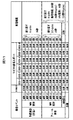
- a processing sample 1 shown in FIG. 13 includes a silicon (Si) substrate (Si-Sub), a thermal oxide film SiO 2 formed on the Si substrate, and a P-doped layer formed on the thermal oxide film SiO 2. It has a Si film.
- the thickness of the thermal oxide film SiO 2 is about 1000 mm.
- This thermal oxide film SiO 2 is, for example, a Si oxide film formed by diffusing oxygen O on the surface of the Si substrate in a 900 ° C. oxygen atmosphere in a vertical substrate processing apparatus provided with a resistance heater.
- the P-doped Si film has a film thickness of about 3000 mm and a P concentration of 1e 21 atoms / cm 3 .
- This P-doped Si film is formed, for example, in a vertical substrate processing apparatus equipped with a resistance heater, and SiH 4 (monosilane) and PH 3 (phosphine: (Phosphine) is introduced and deposited and formed on a substrate that has been transported and fixed in the reaction chamber in advance.
- SiH 4 monosilane
- PH 3 phosphine: (Phosphine)
- the processing sample 2 shown in FIG. 14 includes an Si substrate, a thermal oxide film SiO 2 formed on the Si substrate, a first P-doped Si film formed on the thermal oxide film SiO 2 , An amorphous Si film containing no phosphorus (Non-doped Si) formed on the first P-doped Si film, and a second P-doped containing P formed on the Non-doped Si film And a Si film.
- the thickness of the thermal oxide film SiO 2 is about 1000 mm.
- the P concentration of the first and second P-doped Si films is 1e 21 atoms / cm 3 .
- the first and second P-doped Si films are formed, for example, by introducing SiH 4 and PH 3 into a reaction chamber under reduced pressure at a reaction chamber temperature of 500 to 650 ° C. in a vertical substrate processing apparatus equipped with a resistance heater. The film is deposited and formed on a substrate that has been transported and fixed in the reaction chamber in advance.
- Non-doped Si (amorphous Si film) is prepared by introducing SiH 4 into a reaction chamber under reduced pressure at a reaction chamber temperature of 500 to 650 ° C., for example, in a vertical substrate processing apparatus equipped with a resistance heater. It is deposited and deposited on a substrate that has been transported and fixed in the room.
- the film thickness of the second P-doped Si film / Non-doped Si film / first P-doped Si film is about 3000 mm.
- the processing sample 1 was subjected to the following microwave annealing (MWA) processing, annealing processing by interval microwave irradiation described in Example 2, and Furnace Anneal (FA).
- MWA microwave annealing
- FA Furnace Anneal
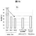
- the MWA treatment is performed by performing an annealing treatment for 150 seconds on the processing sample 1 with microwave outputs of 4 kW, 6 kW, and 10 kW.
- FA is an annealing process in which a processing sample 1 as an object to be processed is subjected to a predetermined time at a desired temperature in an atmospheric pressure and N 2 atmosphere in a vertical substrate processing apparatus including a resistance heater.
- Rs measured by the four-probe method is one of the quantities representing the electric resistance of a thin film or a film-like substance having a uniform thickness, and represents the difficulty of conducting electricity of the substance or material.
- the Rs of the P-doped Si film decreases as the microwave output increases.
- the Hall mobility at this time is improved as the microwave output is increased, and becomes about 21 cm 2 / Vs at the microwave output (10 kW).
- the peak temperature of the treated sample 1 at this time is 820 ° C.
- FIG. 17 is based on SIMS (Secondary Ion Mass Spectrometry, Secondary Ion Mass Spectrometry) when the treated sample 2 was annealed by MWA and FA performed under the following conditions and interval microwave irradiation of Example 2. The cross-sectional concentration distribution of P is shown.
- the MWA in FIG. 17 corresponds to the annealing process for 150 seconds (150 s) with a microwave output of 10 kW and the annealing process for 60 seconds (60 s) with a microwave output of 10 kW (the annealing process of Example 1). ) Is performed on the processing sample 2.
- P is an amorphous Si film containing no phosphorus (Non from the first and second P-doped Si films).
- -Doped Si Non from the first and second P-doped Si films
- the non-doped Si film also has a P concentration of about 1.5e 19 atoms / cm 3 .
- MWA and FA performed at a processing time of 150 seconds, the substrate surface and the film surface are heated by radiation from a resistance heater, and further, the inside of the substrate and the film are heated by heat transfer from the surface. Annealing by temperature is performed. That is, it is considered that P is likely to diffuse because heating is performed in a state where the substrate temperature and the film temperature are substantially the same or higher on the outside.
- the M diffusion for 60 seconds (corresponding to the annealing process of Example 1) and the annealing process by the interval microwave irradiation of Example 2 can suppress the diffusion of P.
- the diffusion of P can be further suppressed by the microwave output of 10 kW corresponding to the annealing process of Example 1 than the MWA of 60 seconds.
- the reason for this is that by performing the interval microwave irradiation of Example 2, an increase in the temperature of the substrate of the processing sample 2 can be suppressed as compared with the case where the MWA that continues the microwave irradiation described above is performed for 60 seconds.
- the first and second P-doped Si films are selectively and locally heated by the action of waves, and P diffusion can be suppressed. (4) Effects according to this embodiment According to this embodiment, one or more of the following effects can be obtained.
- the heating of the wafer 200 is controlled by changing the ratio of the time to turn on the power of the microwave oscillator 655 and the time to turn it off based on the measured temperature of the wafer 200. Thereby, the peak temperature of the wafer 200 in the annealing process can be lowered. Moreover, it is possible to suppress the occurrence of hot spots on the wafer 200 and to suppress the deformation of the wafer (when the susceptor is mounted, the susceptor is also the same as the wafer 200).
- the controller 121 controls the power source of the microwave oscillator 655 to be turned on and off. Since complicated control such as controlling the output of the microwave oscillator is not performed, the control complexity of the controller 121 can be avoided.
- a plurality of microwave oscillators are provided, and the controller 121 controls the microwave irradiation as a plurality of events.
- the controller 121 controls the power on and off of the plurality of microwave oscillators so that the microwave input power supplied to the wafer 200 is constant at each event during microwave irradiation.
- Such control makes it possible to suppress the concentration of a load on a specific microwave oscillator, and to avoid the complexity of control of the microwave oscillator.
- the controller 121 performs control so that the periods during which the power sources of the plurality of microwave supply sources are turned off are different at each event during microwave irradiation. By shifting the microwave oscillator whose power is turned off at each event, it is possible to avoid that the output of the microwave supplied to the case 102 becomes 0 kW when each event is switched.
- the temperature of the wafer 200 is adjusted to a desired temperature without adjusting the output of the microwave oscillator by adjusting the microwave irradiation time, the microwave irradiation stop time, and the number of repetitions thereof. Control to the belt becomes possible.
- the temperature adjustment step By applying it to the temperature adjustment step, the generation of hot spots in the wafer 200 surface can be reduced, so that the distortion of the semiconductor substrate can be reduced.
- the annealing process it is possible to reduce the occurrence of hot spots in the wafer 200 surface, so that the processing in the wafer 200 surface can be made uniform.
- this embodiment is configured as a so-called vertical batch type substrate processing apparatus capable of holding a plurality of substrates in multiple vertical stages.
- a boat 217 serving as a substrate holder is provided with a plurality of wafers 200 held in multiple vertical stages to be processed, and heat insulating plates placed vertically above and below the wafers 200 so as to sandwich the plurality of wafers 200.
- Quartz plates 101a and 101b are held at a predetermined interval.
- a quartz plate 101c as a heat insulating plate is provided between the wafers 200 held in multiple stages in the vertical direction.
- Other configurations are the same as those in FIG. 1, and the description thereof is omitted.
- FIG. 19 is also configured as a so-called vertical batch type substrate processing apparatus capable of holding a plurality of substrates in multiple vertical stages.
- the boat 217 includes a plurality of wafers 200 held in multiple vertical stages to be processed, and a quartz plate 101a as a heat insulating plate placed vertically above and below the wafers 200 so as to sandwich the plurality of wafers 200. 101b is held at a predetermined interval.
- the boat 217 holds wafers 200 to be processed between the quartz plates 101a and 101b as heat insulating plates and between the quartz plates 101c and 101d as heat insulating plates. Between the wafer 200 and the quartz plates 101a and 101b, susceptors 1011a and 1011b are held as heating elements that are dielectrically heated by electromagnetic waves. Further, between the wafer 200 and the quartz plates 101c and 101d, susceptors 1011c and 1011d are held as heating elements that are dielectrically heated by electromagnetic waves.
- the process of modifying an amorphous silicon film into a polysilicon film as a film containing silicon as a main component has been described.
- the present invention is not limited thereto, and oxygen (O), nitrogen (N),
- the film formed on the surface of the wafer 200 may be modified by supplying a gas containing at least one of carbon (C) and hydrogen (H).
- a hafnium oxide film (HfxOy film) as a high dielectric film is formed on the wafer 200, by supplying a microwave and heating while supplying a gas containing oxygen, the hafnium oxide film
- the deficient oxygen can be replenished to improve the characteristics of the high dielectric film.
- the present invention is not limited to this, but aluminum (Al), titanium (Ti), zirconium (Zr), tantalum (Ta), niobium (Nb), lanthanum (La), cerium ( An oxide film containing a metal element containing at least one of Ce), yttrium (Y), barium (Ba), strontium (Sr), calcium (Ca), lead (Pb), molybdenum (Mo), tungsten (W), etc.
- the present invention can be suitably applied to the case of modifying a metal oxide film.
- the film formation sequence described above is performed on the wafer 200 on the TiOCN film, the TiOC film, the TiON film, the TiO film, the ZrOCN film, the ZrOC film, the ZrON film, the ZrO film, the HfOCN film, the HfOC film, the HfON film, the HfO film, TaOCN film, TaOC film, TaON film, TaO film, NbOCN film, NbOC film, NbON film, NbO film, AlOCN film, AlOC film, AlON film, AlO film, MoOCN film, MoOC film, MoON film, MoO film, WOCN film
- the present invention can be suitably applied to the case of modifying the WOC film, the WON film, and the WO film.
- a film mainly composed of silicon doped with impurities may be heated.
- a film mainly composed of silicon a silicon nitride film (SiN film), a silicon oxide film (SiO film), a silicon oxycarbide film (SiOC film), a silicon oxycarbonitride film (SiOCN film), a silicon oxynitride film (SiON)
- the impurity include at least one of bromine (B), carbon (C), nitrogen (N), aluminum (Al), phosphorus (P), gallium (Ga), arsenic (As), and the like.
- it may be a resist film based on at least one of methyl methacrylate resin (PMMA), epoxy resin, novolac resin, polyvinyl phenyl resin, and the like.
- PMMA methyl methacrylate resin
- epoxy resin epoxy resin
- novolac resin polyvinyl phenyl resin
- the present invention is not limited to this. Patterning process in the liquid crystal panel manufacturing process, patterning process in the solar cell manufacturing process, and patterning process in the power device manufacturing process.
- the present invention can also be applied to a technique for processing a substrate.
Landscapes
- Physics & Mathematics (AREA)
- Electromagnetism (AREA)
- Health & Medical Sciences (AREA)
- Clinical Laboratory Science (AREA)
- General Health & Medical Sciences (AREA)
- Engineering & Computer Science (AREA)
- Plasma & Fusion (AREA)
- Chemical & Material Sciences (AREA)
- Analytical Chemistry (AREA)
- Recrystallisation Techniques (AREA)
- Constitution Of High-Frequency Heating (AREA)
- Toxicology (AREA)
- Automation & Control Theory (AREA)
- Optics & Photonics (AREA)
Abstract
Description
以下に本発明の一実施形態を図面に基づいて説明する。
(1)基板処理装置の構成
本実施の形態において、本発明に係る基板処理装置100は、ウエハに各種の熱処理を施す枚葉式熱処理装置として構成されている。本実施の形態において基板処理装置100は後述する電磁波を用いたアニール処理(改質処理)を行う装置として説明を行う。
(処理室)
図1に示すように、本実施形態に係る基板処理装置100は、金属などの電磁波を反射する材料で構成されるキャビティ(上部容器)としてのケース102と、ケース102の内部に収容され、垂直方向の上下端部が開放された円筒形状の反応管103を有している。反応管103は、石英などの電磁波を透過する材料で構成される。また、金属材料で構成されたキャップフランジ(閉塞板)104が、封止部材(シール部材)としてのOリング220を介して反応管103の上端と当接されて反応管103の上端を閉塞する。主にケース102と反応管103、および、キャップフランジ104によってシリコンウエハ等の基板を処理する処理容器を構成し、特に反応管103の内側空間を処理室201として構成している。反応管103を設けずに、ケース102、キャップフランジ104により処理容器を構成するようにしてもよい。その場合、ケース102の内部空間が処理室201となる。また、キャップフランジ104を設けずに、天井が閉塞したケース102を用いて、ケース102と反応管103、または、ケース102によって処理容器を構成するようにしてもよい。
(排気部)
処理室201の下方であって、載置台210の外周側には、処理室201の雰囲気を排気する排気部が設けられている。図1に示すように、排気部には排気口221が設けられている。排気口221には排気管231が接続されており、排気管231には、処理室201内の圧力に応じて弁開度を制御するAPCバルブなどの圧力調整器244、真空ポンプ246が順に直列に接続されている。
(ガス供給部)
キャップフランジ104には、不活性ガス、原料ガス、反応ガスなどの各種基板処理のための処理ガスを処理室201内に供給するためのガス供給管232が設けられている。
(温度センサ)
キャップフランジ104には、非接触式の温度測定装置として温度センサ263が設置されている。温度センサ263により検出された温度情報に基づき後述するマイクロ波発振器655の出力を調整することで、基板を加熱し、基板温度が所望の温度分布となる。温度センサ263は、例えばIR(Infrared Radiation)センサなどの放射温度計で構成されている。温度センサ263は、石英プレート101aの表面温度、または、ウエハ200の表面温度を測定するように設置される。上述した発熱体としてのサセプタが設けられている場合にはサセプタの表面温度を測定するように構成してもよい。なお、本発明においてウエハ200の温度(ウエハ温度)と記載した場合は、後述する温度変換データによって変換されたウエハ温度、すなわち、推測されたウエハ温度のことを意味する場合と、温度センサ263によって直接ウエハ200の温度を測定して取得した温度を意味する場合と、それらの両方を意味する場合を指すものとして説明する。
(電磁波供給部)
図3は、図面の複雑さを避けるため、マイクロ波発振器の図示は省略されている。
(制御装置)
図6に示すように、制御部(制御装置、制御手段)であるコントローラ121は、CPU(Central Processing Unit)121a、RAM(Random Access Memory)121b、記憶装置121c、I/Oポート121dを備えたコンピュータとして構成されている。RAM121b、記憶装置121c、I/Oポート121dは、内部バス121eを介して、CPU121aとデータ交換可能なように構成されている。コントローラ121には、例えばタッチパネル等として構成された入出力装置122が接続されている。
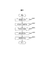
(2)基板処理工程
次に、基板処理装置100の処理炉を用いた基板処理方法を説明する。ここ説明される基板処理方法では、上述の基板処理装置100の処理炉を用いて、半導体装置(デバイス)の製造工程の一工程、例えば、基板上に形成されたシリコン含有膜としてのアモルファスシリコン膜の改質(結晶化)工程の一例について図7に示した処理フローに沿って説明する。以下の説明において、基板処理装置100を構成する各部の動作はコントローラ121により制御される。
(基板搬入工程(S401))
図1に示されているように、所定枚数のウエハ200がボート217に移載されると、駆動機構267は、載置台210を上昇させることでボート217を反応管103内側の処理室201に搬入(ボートローディング)する(S401)。
(炉内圧力・温度調整工程(S402))
処理室201内へのボート217の搬入が完了したら、処理室201内が所定の圧力(例えば10~102000Pa)となるよう処理室201内の雰囲気を制御する。具体的には、真空ポンプ246により排気しつつ、圧力センサ245により検出された圧力情報に基づいて圧力調整器244の弁開度をフィードバック制御し、処理室201内を所定の圧力とする。また、同時に予備加熱として電磁波供給部を制御し、所定の温度まで加熱を行うように制御してもよい(S402)。電磁波供給部によって、所定の基板処理温度まで昇温させる場合、ウエハ200が変形・破損しないように、後述する改質工程の出力よりも小さな出力で昇温を行うことが好ましい。なお、大気圧下で基板処理を行う場合、炉内圧力調整を行わず、炉内の温度調整のみを行った後、後述する不活性ガス供給工程S403へ移行するように制御してもよい。
(不活性ガス供給工程(S403))
炉内圧力・温度調整工程S402によって処理室201内の圧力と温度を所定の値に制御すると、駆動機構267は、シャフト255を回転させ、載置台210上のボート217を介してウエハ200を回転させる。このとき、窒素ガス等の不活性ガスがガス供給管232を介して供給される(S403)。さらにこのとき、処理室201内の圧力は10Pa以上102000Pa以下の範囲となる所定の値であって、例えば101300Pa以上101650Pa以下となるように調整される。なお、シャフトは基板搬入工程S401時、すなわち、ウエハ200を処理室201内に搬入完了後に回転させてもよい。また、本工程は炉内圧力調整方法として炉内圧力・温度調整工程S402と同時に実施されてもよい。
(改質工程(S404))
処理室201内を所定の圧力となるように維持すると、マイクロ波発振器655は上述した各部を介して処理室201内にマイクロ波を供給する。処理室201内にマイクロ波が供給されることによって、ウエハ200が100℃以上、1000℃以下の温度、好適には400℃以上、900℃以下の温度となるように加熱し、さらに好適には、500℃以上、700℃以下の温度となるように加熱する。このような温度で基板処理することによって、ウエハ200が効率よくマイクロ波を吸収する温度下での基板処理となり、改質処理の速度向上が可能となる。換言すると、ウエハ200の温度を100℃よりも低い温度、または1000℃よりも高い温度下で処理してしまうと、ウエハ200の表面が変質してしまい、マイクロ波を吸収し難くなってしまうためにウエハ200を加熱し難くなってしまうこととなる。このため、上述した温度帯で基板処理を行うことが望まれる。このような基板処理の温度帯を維持するために、改質処理(アニール処理)中に冷却処理を行うことが好ましい。
(搬出工程(S405))
処理室201内の圧力を大気圧復帰させた後に、駆動機構267は載置台210を下降させることにより、炉口を開口するとともに、ボート217を搬送空間203に搬出(ボートアンローディング)する。その後ボートに載置されているウエハ200を搬送空間23の外部に位置する搬送室に搬出する(S405)。
(3)温度制御方法
以下に、上述した炉内圧力・温度調整工程S402及び改質工程S404におけるマイクロ波の照射方法を制御することによる温度制御方法について、図面を用いて説明する。以下の説明において、マイクロ波発振器655の出力(POWER)とは、ケース102内または処理室201内に照射されるマイクロ波の入力電力を意味する。また、図1および図3に示されるように、複数のマイクロ波発振器655-1~655-6が設けられる場合、特に記載がない場合、マイクロ波発振器655の出力とは、複数のマイクロ波発振器655-1~655-6から照射される各マイクロ波の出力の合計を意味する。
(実施例1)
実施例1における炉内圧力・温度調整工程S402及び改質工程S404におけるマイクロ波の照射方法について、図8を用いて説明する。図8において、縦軸は温度(T℃)であり、横軸は時間(秒:sec)である。
(実施例2)
次に、実施例2における炉内圧力・温度調整工程S402及び改質工程S404におけるマイクロ波の照射方法について、図9を用いて説明する。実施例2におけるマイクロ波の照射方法が、実施例1と異なる点は、改質工程のアニール処理において、ウエハ200の処理温度が一定の温度範囲内で上下するようにマイクロ波の照射とマイクロ波の照射停止とを交互に繰り返す点である。その他の点は、特に言及しない限りは、実施例1と同様である。
(実施例3)
次に、実施例3における炉内圧力・温度調整工程S402及び改質工程S404におけるマイクロ波の照射方法について、図10を用いて説明する。実施例3におけるマイクロ波の照射方法が、実施例1、2と異なる点は、改質工程のアニール処理において、複数設けられたマイクロ波導入ポートから供給されるマイクロ波を所定の順番で供給停止し、処理室に供給されるマイクロ波出力を一定とし、マイクロ波導入ポートからのマイクロ波供給を一通り停止した後に、全てのマイクロ波導入ポートからのマイクロ波供給を停止する点である。その他の点は、特に言及しない限りは、実施例1、2と同様である。
(実施例4)
次に、実施例4における炉内圧力・温度調整工程S402及び改質工程S404におけるマイクロ波の照射方法について、図11、図12を用いて説明する。実施例4におけるマイクロ波の照射方法が、実施例3と異なる点は、予備加熱処理においても、複数設けられたマイクロ波導入ポートから供給されるマイクロ波を所定の順番で供給停止し、処理室に供給されるマイクロ波出力を一定とする点である。その他の点は、特に言及しない限りは、実施例1、2、3と同様である。なお、以下で説明されるように、実施例4では、予備加熱処理において上述のサイクルマイクロ波(MW)照射が繰り返して実行され、また、改質工程のアニール処理において上述のサイクルマイクロ波(MW)照射の繰り返しとマイクロ波停止のイベントとの組み合わせが繰り返し実行される。
(実験結果の一例)
上述した実施例を用いて実際に実験を行った結果について以下に説明する。
(4)本実施形態による効果
本実施形態によれば以下に示す1つまたは複数の効果が得られる。
図18に示すように本実施形態では、垂直方向多段に基板を複数枚保持可能な、いわゆる、縦型バッチ式の基板処理装置として構成している。基板保持具としてのボート217には、処理対象である垂直方向多段に保持された複数のウエハ200と、この複数のウエハ200を挟み込むようにウエハ200の垂直方向上下に載置された断熱板としての石英プレート101a、101bが所定の間隔で保持されている。垂直方向多段に保持されたウエハ200間に断熱板としての石英プレート101cが設けられている。他の構成は、図1と同じであり、その説明は省略される。
(変形例1)
図19も、図18と同様に、垂直方向多段に基板を複数枚保持可能な、いわゆる、縦型バッチ式の基板処理装置として構成している。ボート217には、処理対象である垂直方向多段に保持された複数のウエハ200と、この複数のウエハ200を挟み込むようにウエハ200の垂直方向上下に載置された断熱板としての石英プレート101a、101bが所定の間隔で保持されている。図19では、この複数のウエハ200間に、石英プレート101cが設けられていない構成例である。他の構成は、図1と同じであり、その説明は省略される。ボート217に保持するウエハ200を3枚として記載しているが、これに限らず、例えば25枚や50枚など多数枚のウエハ200を処理するようにしてもよい。
(変形例2)
図20に示すように、ボート217には、断熱板としての石英プレート101a、101bの間及び断熱板としての石英プレート101c、101dの間に、処理対象であるウエハ200が各々保持されている。ウエハ200と石英プレート101a、101bの間には、電磁波によって誘電加熱される発熱体としてのサセプタ1011a及び1011bが各々保持されている。また、ウエハ200と石英プレート101c、101dの間には、電磁波によって誘電加熱される発熱体としてのサセプタ1011c及び1011dが各々保持されている。
102・・・ケース(キャビティ)、
103・・・反応管、
121・・・コントローラ(制御部)、
200・・・ウエハ(基板)、
201・・・処理室、
217・・・ボート(基板保持具)、
655・・・マイクロ波発振器。
Claims (5)
- 基板を処理する処理室と、
前記処理室内の基板を加熱するためのマイクロ波を供給する複数のマイクロ波供給源を有する加熱装置と、
前記複数のマイクロ波供給源のそれぞれから前記基板に対して供給されるマイクロ波の入力電力を一定としつつ、前記複数のマイクロ波供給源がオフとなる期間がそれぞれ異なるように前記複数のマイクロ波供給源を制御するよう構成される制御部と、
を有する基板処理装置。 - 前記制御部は、前記複数のマイクロ波供給源が所定の順番にオフとなることを確認した後に、全マイクロ波供給源をオフとするように前記複数のマイクロ波供給源を制御するよう構成される請求項1に記載の基板処理装置。
- 前記制御部は、前記基板へ供給される入力電力は2kW以上、24kW以下となるように前記加熱装置を制御するよう構成される請求項1または2に記載の基板処理装置。
- 基板を処理する処理室と、前記処理室内の基板を加熱するためのマイクロ波を供給する複数のマイクロ波供給源を有する加熱装置と、前記複数のマイクロ波供給源のそれぞれから前記基板に対して供給されるマイクロ波の入力電力を一定としつつ、前記複数のマイクロ波供給源がオフとなる期間がそれぞれ異なるように前記複数のマイクロ波供給源を制御するよう構成される制御部と、を有する基板処理装置の前記処理室内に前記基板を保持した基板保持具を搬入する工程と、
前記基板を加熱して所定の改質処理を行う工程と、
前記処理室から前記基板保持具を搬出する工程と、
を有する半導体装置の製造方法。 - 基板を処理する処理室と、前記処理室内の基板を加熱するためのマイクロ波を供給する複数のマイクロ波供給源を有する加熱装置と、前記複数のマイクロ波供給源のそれぞれから前記基板に対して供給されるマイクロ波の入力電力を一定としつつ、前記複数のマイクロ波供給源がオフとなる期間がそれぞれ異なるように前記複数のマイクロ波供給源を制御するよう構成される制御部と、を有する基板処理装置の前記処理室内に前記基板を保持した基板保持具を搬入する手順と、
前記基板を加熱して所定の改質処理を行う手順と、
前記処理室から前記基板保持具を搬出する手順と、
をコンピュータによって前記基板処理装置に実行させるためのプログラム。
Priority Applications (4)
| Application Number | Priority Date | Filing Date | Title |
|---|---|---|---|
| PCT/JP2017/009610 WO2018163386A1 (ja) | 2017-03-09 | 2017-03-09 | 基板処理装置、半導体装置の製造方法およびプログラム |
| JP2019504252A JP6821788B2 (ja) | 2017-03-09 | 2017-03-09 | 基板処理装置、半導体装置の製造方法およびプログラム |
| KR1020197025508A KR102259316B1 (ko) | 2017-03-09 | 2017-03-09 | 기판 처리 장치, 반도체 장치의 제조 방법 및 프로그램 |
| US16/554,557 US11264253B2 (en) | 2017-03-09 | 2019-08-28 | Substrate processing apparatus, method of manufacturing semiconductor device, and recording medium |
Applications Claiming Priority (1)
| Application Number | Priority Date | Filing Date | Title |
|---|---|---|---|
| PCT/JP2017/009610 WO2018163386A1 (ja) | 2017-03-09 | 2017-03-09 | 基板処理装置、半導体装置の製造方法およびプログラム |
Related Child Applications (1)
| Application Number | Title | Priority Date | Filing Date |
|---|---|---|---|
| US16/554,557 Continuation US11264253B2 (en) | 2017-03-09 | 2019-08-28 | Substrate processing apparatus, method of manufacturing semiconductor device, and recording medium |
Publications (1)
| Publication Number | Publication Date |
|---|---|
| WO2018163386A1 true WO2018163386A1 (ja) | 2018-09-13 |
Family
ID=63447486
Family Applications (1)
| Application Number | Title | Priority Date | Filing Date |
|---|---|---|---|
| PCT/JP2017/009610 Ceased WO2018163386A1 (ja) | 2017-03-09 | 2017-03-09 | 基板処理装置、半導体装置の製造方法およびプログラム |
Country Status (4)
| Country | Link |
|---|---|
| US (1) | US11264253B2 (ja) |
| JP (1) | JP6821788B2 (ja) |
| KR (1) | KR102259316B1 (ja) |
| WO (1) | WO2018163386A1 (ja) |
Cited By (5)
| Publication number | Priority date | Publication date | Assignee | Title |
|---|---|---|---|---|
| WO2021100107A1 (ja) * | 2019-11-19 | 2021-05-27 | 株式会社Kokusai Electric | 基板処理装置および半導体装置の製造方法 |
| WO2022054750A1 (ja) * | 2020-09-09 | 2022-03-17 | 株式会社Kokusai Electric | 基板処理装置、半導体装置の製造方法およびプログラム |
| JP2022051437A (ja) * | 2020-09-18 | 2022-03-31 | 株式会社Kokusai Electric | 基板処理装置、基板保持具、及び、半導体装置の製造方法 |
| JP2022182381A (ja) * | 2021-05-28 | 2022-12-08 | 株式会社Kokusai Electric | 基板処理装置、半導体装置の製造方法、基板処理方法およびプログラム |
| TWI792039B (zh) * | 2019-08-14 | 2023-02-11 | 南韓商細美事有限公司 | 支撐單元、包括支撐單元的基板處理設備及基板處理方法 |
Families Citing this family (5)
| Publication number | Priority date | Publication date | Assignee | Title |
|---|---|---|---|---|
| CN112423418B (zh) * | 2020-08-25 | 2021-11-09 | 昆明理工大学 | 一种流体物料微波加热装置及其智能控制方法 |
| JP1700778S (ja) * | 2021-03-15 | 2021-11-29 | 基板処理装置用遮蔽具 | |
| US12546690B2 (en) * | 2021-03-31 | 2026-02-10 | The Research Foundation For The State University Of New York | Systems and methods for annealing samples |
| JP7571073B2 (ja) * | 2022-03-24 | 2024-10-22 | 株式会社Kokusai Electric | 半導体装置の製造方法、基板処理方法、プログラム、及び基板処理装置 |
| US20240047552A1 (en) * | 2022-08-04 | 2024-02-08 | Taiwan Semiconductor Manufacturing Company, Ltd. | Structure and Method for Deep Trench Capacitor with Reduced Deformation |
Citations (4)
| Publication number | Priority date | Publication date | Assignee | Title |
|---|---|---|---|---|
| JPH0456090A (ja) * | 1990-06-21 | 1992-02-24 | Matsushita Electric Ind Co Ltd | 高周波加熱装置 |
| JPH0590885U (ja) * | 1991-04-10 | 1993-12-10 | 四国計測工業株式会社 | マイクロ波加熱装置 |
| JP2012084510A (ja) * | 2010-09-14 | 2012-04-26 | Tokyo Electron Ltd | マイクロ波照射装置およびマイクロ波照射方法 |
| JP2013058652A (ja) * | 2011-09-09 | 2013-03-28 | Tokyo Electron Ltd | マイクロ波処理装置およびその制御方法 |
Family Cites Families (8)
| Publication number | Priority date | Publication date | Assignee | Title |
|---|---|---|---|---|
| JP3189324B2 (ja) | 1991-09-28 | 2001-07-16 | 株式会社村田製作所 | 弾性表面波装置の実装方法 |
| US20040235281A1 (en) * | 2003-04-25 | 2004-11-25 | Downey Daniel F. | Apparatus and methods for junction formation using optical illumination |
| US20070167029A1 (en) * | 2005-11-11 | 2007-07-19 | Kowalski Jeffrey M | Thermal processing system, components, and methods |
| JP5358580B2 (ja) * | 2008-09-17 | 2013-12-04 | パナソニック株式会社 | マイクロ波加熱装置 |
| JP6188145B2 (ja) | 2013-09-27 | 2017-08-30 | 株式会社日立国際電気 | 基板処理装置、半導体装置の製造方法及びプログラム |
| JP6163442B2 (ja) * | 2014-03-05 | 2017-07-12 | 株式会社東芝 | 半導体製造装置及び半導体装置の製造方法 |
| JP5916909B1 (ja) * | 2015-02-06 | 2016-05-11 | 株式会社日立国際電気 | 基板処理装置、ガス整流部、半導体装置の製造方法およびプログラム |
| JP2016186991A (ja) * | 2015-03-27 | 2016-10-27 | 株式会社日立国際電気 | 基板処理装置、半導体装置の製造方法およびプログラム |
-
2017
- 2017-03-09 JP JP2019504252A patent/JP6821788B2/ja active Active
- 2017-03-09 KR KR1020197025508A patent/KR102259316B1/ko active Active
- 2017-03-09 WO PCT/JP2017/009610 patent/WO2018163386A1/ja not_active Ceased
-
2019
- 2019-08-28 US US16/554,557 patent/US11264253B2/en active Active
Patent Citations (4)
| Publication number | Priority date | Publication date | Assignee | Title |
|---|---|---|---|---|
| JPH0456090A (ja) * | 1990-06-21 | 1992-02-24 | Matsushita Electric Ind Co Ltd | 高周波加熱装置 |
| JPH0590885U (ja) * | 1991-04-10 | 1993-12-10 | 四国計測工業株式会社 | マイクロ波加熱装置 |
| JP2012084510A (ja) * | 2010-09-14 | 2012-04-26 | Tokyo Electron Ltd | マイクロ波照射装置およびマイクロ波照射方法 |
| JP2013058652A (ja) * | 2011-09-09 | 2013-03-28 | Tokyo Electron Ltd | マイクロ波処理装置およびその制御方法 |
Cited By (9)
| Publication number | Priority date | Publication date | Assignee | Title |
|---|---|---|---|---|
| TWI792039B (zh) * | 2019-08-14 | 2023-02-11 | 南韓商細美事有限公司 | 支撐單元、包括支撐單元的基板處理設備及基板處理方法 |
| US12278121B2 (en) | 2019-08-14 | 2025-04-15 | Semes Co., Ltd. | Support unit, substrate treating apparatus including the same, and substrate treating method |
| WO2021100107A1 (ja) * | 2019-11-19 | 2021-05-27 | 株式会社Kokusai Electric | 基板処理装置および半導体装置の製造方法 |
| WO2022054750A1 (ja) * | 2020-09-09 | 2022-03-17 | 株式会社Kokusai Electric | 基板処理装置、半導体装置の製造方法およびプログラム |
| TWI793744B (zh) * | 2020-09-09 | 2023-02-21 | 日商國際電氣股份有限公司 | 基板處理裝置、半導體裝置之製造方法及程式 |
| JP7645273B2 (ja) | 2020-09-09 | 2025-03-13 | 株式会社Kokusai Electric | 基板処理装置、半導体装置の製造方法およびプログラム |
| JP2022051437A (ja) * | 2020-09-18 | 2022-03-31 | 株式会社Kokusai Electric | 基板処理装置、基板保持具、及び、半導体装置の製造方法 |
| JP7361005B2 (ja) | 2020-09-18 | 2023-10-13 | 株式会社Kokusai Electric | 基板処理装置、基板保持具、半導体装置の製造方法、及び、プログラム |
| JP2022182381A (ja) * | 2021-05-28 | 2022-12-08 | 株式会社Kokusai Electric | 基板処理装置、半導体装置の製造方法、基板処理方法およびプログラム |
Also Published As
| Publication number | Publication date |
|---|---|
| JPWO2018163386A1 (ja) | 2019-12-26 |
| US11264253B2 (en) | 2022-03-01 |
| JP6821788B2 (ja) | 2021-01-27 |
| KR102259316B1 (ko) | 2021-06-01 |
| KR20190112785A (ko) | 2019-10-07 |
| US20200013646A1 (en) | 2020-01-09 |
Similar Documents
| Publication | Publication Date | Title |
|---|---|---|
| US11264253B2 (en) | Substrate processing apparatus, method of manufacturing semiconductor device, and recording medium | |
| JP6454425B2 (ja) | 半導体装置の製造方法、基板処理装置およびプログラム | |
| JP6838010B2 (ja) | 基板処理装置、半導体装置の製造方法およびプログラム | |
| JP6748720B2 (ja) | 基板処理装置、半導体装置の製造方法およびプログラム | |
| JP7222003B2 (ja) | 基板処理装置、基板保持装置、半導体装置の製造方法およびプログラム | |
| KR102118268B1 (ko) | 반도체 장치의 제조 방법, 기판 처리 장치 및 프로그램 | |
| JP7033651B2 (ja) | 基板処理装置、半導体装置の製造方法、プログラム、および、基板処理方法 | |
| KR102294007B1 (ko) | 반도체 장치의 제조 방법, 기판 처리 장치 및 기록 매체 | |
| KR102822702B1 (ko) | 기판 처리 장치, 반도체 장치의 제조 방법 및 프로그램 | |
| KR102204253B1 (ko) | 발열체, 기판 처리 장치 및 반도체 장치의 제조 방법 | |
| TWI793744B (zh) | 基板處理裝置、半導體裝置之製造方法及程式 | |
| KR20250001423A (ko) | 기판 처리 장치, 기판 처리 방법, 반도체 장치의 제조 방법 및 프로그램 | |
| JP2024099858A (ja) | 基板処理装置、基板処理方法、半導体装置の製造方法およびプログラム | |
| WO2019053805A1 (ja) | 基板処理装置、半導体装置の製造方法およびプログラム | |
| JP6949080B2 (ja) | 基板処理装置、半導体装置の製造方法およびプログラム | |
| WO2025158724A1 (ja) | 基板処理方法、半導体装置の製造方法、基板処理装置、およびプログラム | |
| JP2023143716A (ja) | 基板処理装置、半導体装置の製造方法およびプログラム |
Legal Events
| Date | Code | Title | Description |
|---|---|---|---|
| 121 | Ep: the epo has been informed by wipo that ep was designated in this application |
Ref document number: 17899861 Country of ref document: EP Kind code of ref document: A1 |
|
| ENP | Entry into the national phase |
Ref document number: 2019504252 Country of ref document: JP Kind code of ref document: A |
|
| ENP | Entry into the national phase |
Ref document number: 20197025508 Country of ref document: KR Kind code of ref document: A |
|
| NENP | Non-entry into the national phase |
Ref country code: DE |
|
| 122 | Ep: pct application non-entry in european phase |
Ref document number: 17899861 Country of ref document: EP Kind code of ref document: A1 |