WO2018159130A1 - 液晶表示装置およびこの液晶表示装置に用いられる一対の光学フィルム - Google Patents
液晶表示装置およびこの液晶表示装置に用いられる一対の光学フィルム Download PDFInfo
- Publication number
- WO2018159130A1 WO2018159130A1 PCT/JP2018/001300 JP2018001300W WO2018159130A1 WO 2018159130 A1 WO2018159130 A1 WO 2018159130A1 JP 2018001300 W JP2018001300 W JP 2018001300W WO 2018159130 A1 WO2018159130 A1 WO 2018159130A1
- Authority
- WO
- WIPO (PCT)
- Prior art keywords
- liquid crystal
- optical film
- group
- crystal display
- display device
- Prior art date
- Legal status (The legal status is an assumption and is not a legal conclusion. Google has not performed a legal analysis and makes no representation as to the accuracy of the status listed.)
- Ceased
Links
Images
Classifications
-
- G—PHYSICS
- G02—OPTICS
- G02F—OPTICAL DEVICES OR ARRANGEMENTS FOR THE CONTROL OF LIGHT BY MODIFICATION OF THE OPTICAL PROPERTIES OF THE MEDIA OF THE ELEMENTS INVOLVED THEREIN; NON-LINEAR OPTICS; FREQUENCY-CHANGING OF LIGHT; OPTICAL LOGIC ELEMENTS; OPTICAL ANALOGUE/DIGITAL CONVERTERS
- G02F1/00—Devices or arrangements for the control of the intensity, colour, phase, polarisation or direction of light arriving from an independent light source, e.g. switching, gating or modulating; Non-linear optics
- G02F1/01—Devices or arrangements for the control of the intensity, colour, phase, polarisation or direction of light arriving from an independent light source, e.g. switching, gating or modulating; Non-linear optics for the control of the intensity, phase, polarisation or colour
- G02F1/13—Devices or arrangements for the control of the intensity, colour, phase, polarisation or direction of light arriving from an independent light source, e.g. switching, gating or modulating; Non-linear optics for the control of the intensity, phase, polarisation or colour based on liquid crystals, e.g. single liquid crystal display cells
- G02F1/133—Constructional arrangements; Operation of liquid crystal cells; Circuit arrangements
- G02F1/1333—Constructional arrangements; Manufacturing methods
- G02F1/1335—Structural association of cells with optical devices, e.g. polarisers or reflectors
-
- G—PHYSICS
- G02—OPTICS
- G02F—OPTICAL DEVICES OR ARRANGEMENTS FOR THE CONTROL OF LIGHT BY MODIFICATION OF THE OPTICAL PROPERTIES OF THE MEDIA OF THE ELEMENTS INVOLVED THEREIN; NON-LINEAR OPTICS; FREQUENCY-CHANGING OF LIGHT; OPTICAL LOGIC ELEMENTS; OPTICAL ANALOGUE/DIGITAL CONVERTERS
- G02F1/00—Devices or arrangements for the control of the intensity, colour, phase, polarisation or direction of light arriving from an independent light source, e.g. switching, gating or modulating; Non-linear optics
- G02F1/01—Devices or arrangements for the control of the intensity, colour, phase, polarisation or direction of light arriving from an independent light source, e.g. switching, gating or modulating; Non-linear optics for the control of the intensity, phase, polarisation or colour
- G02F1/13—Devices or arrangements for the control of the intensity, colour, phase, polarisation or direction of light arriving from an independent light source, e.g. switching, gating or modulating; Non-linear optics for the control of the intensity, phase, polarisation or colour based on liquid crystals, e.g. single liquid crystal display cells
- G02F1/133—Constructional arrangements; Operation of liquid crystal cells; Circuit arrangements
- G02F1/1333—Constructional arrangements; Manufacturing methods
- G02F1/1335—Structural association of cells with optical devices, e.g. polarisers or reflectors
- G02F1/133509—Filters, e.g. light shielding masks
-
- G—PHYSICS
- G02—OPTICS
- G02F—OPTICAL DEVICES OR ARRANGEMENTS FOR THE CONTROL OF LIGHT BY MODIFICATION OF THE OPTICAL PROPERTIES OF THE MEDIA OF THE ELEMENTS INVOLVED THEREIN; NON-LINEAR OPTICS; FREQUENCY-CHANGING OF LIGHT; OPTICAL LOGIC ELEMENTS; OPTICAL ANALOGUE/DIGITAL CONVERTERS
- G02F1/00—Devices or arrangements for the control of the intensity, colour, phase, polarisation or direction of light arriving from an independent light source, e.g. switching, gating or modulating; Non-linear optics
- G02F1/01—Devices or arrangements for the control of the intensity, colour, phase, polarisation or direction of light arriving from an independent light source, e.g. switching, gating or modulating; Non-linear optics for the control of the intensity, phase, polarisation or colour
- G02F1/13—Devices or arrangements for the control of the intensity, colour, phase, polarisation or direction of light arriving from an independent light source, e.g. switching, gating or modulating; Non-linear optics for the control of the intensity, phase, polarisation or colour based on liquid crystals, e.g. single liquid crystal display cells
- G02F1/133—Constructional arrangements; Operation of liquid crystal cells; Circuit arrangements
- G02F1/1333—Constructional arrangements; Manufacturing methods
- G02F1/1335—Structural association of cells with optical devices, e.g. polarisers or reflectors
- G02F1/13363—Birefringent elements, e.g. for optical compensation
Definitions
- the present invention relates to a liquid crystal display device excellent in color reproducibility and a pair of optical films used in the liquid crystal display device.
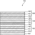
- FIG. 3 is a schematic cross-sectional view of a conventional liquid crystal display device.
- the conventional liquid crystal display device 110 includes a backlight 101, a rear side polarizing plate 102 provided in contact with the backlight 101, and a liquid crystal layer 103 provided in contact with the rear side polarizing plate 102. And a front side polarizing plate 105 provided in contact with the liquid crystal layer 103.
- the rear side optical film 122 is bonded to the viewing side of the rear side polarizer 121
- the rear side protective film 123 is bonded to the non-viewing side of the rear side polarizer 121.
- the front-side polarizing plate 105 has a front-side protective film 152 bonded to the viewing side of the front-side polarizer 151, and a front-side optical film 153 bonded to the non-viewing side of the front-side polarizer 151.
- a liquid crystal cell 132 and a color filter layer 133 provided on the front side of the liquid crystal cell 132 are sandwiched between two cell substrates 106 formed of glass plates.
- the conventional LCD is provided with polarizing plates 102 and 105 on the front surface side and the back surface side of the liquid crystal layer 103, respectively. Attempts have been made to place it in layer 103.
- Patent Document 1 the configuration of a conventional LCD in which a polarizing plate is disposed outside the liquid crystal cell corresponding to the liquid crystal layer 103 shown in FIG. 1 is referred to as “out-cell” and corresponds to the liquid crystal layer 103 shown in FIG.
- the configuration of the liquid crystal display device disclosed in Patent Document 1 in which a polarizing plate is disposed inside the liquid crystal cell is referred to as “in-cell”.
- the parallax of the liquid crystal display device can be improved by changing the arrangement of the polarizing plates from out-cell to in-cell.
- out-sell it is necessary to provide protective films on the front and back of the polarizer, but by changing the configuration of the LCD from out-sell to in-cell, one of the protective films provided on the front and back of the polarizer (on the cell substrate) The optical film on the contact side) can be omitted, and the liquid crystal display device can be thinned.
- Patent Document 2 discloses a technique for forming a color filter layer including quantum dot fine particles. According to the technique disclosed in Patent Document 2, since the layer composed of the quantum dot fine particles and the color filter layer can be integrated, the number of components of the LCD can be reduced and the LCD can be thinned. can do.
- Patent Document 3 discloses a technique for suppressing a reduction in contrast and display unevenness of a liquid crystal display device by adjusting a retardation Rth in the thickness direction of an optical film included in the liquid crystal display device.
- the present invention has been made in view of the above-described present situation, and an object thereof is to provide a liquid crystal display device in which color reproducibility is unlikely to deteriorate.
- One aspect of the present invention includes a non-white light source, a rear-side polarizing plate including a rear-side polarizer and a rear-side optical film, a liquid crystal cell, a light conversion layer that is a color filter containing quantum dot fine particles, and a front side.
- An optical film and a front-side polarizing plate including a front-side polarizer, and a retardation Rth (2) in the thickness direction of the front-side optical film is from ⁇ 10 nm to 10 nm.
- the sum of the thickness direction retardation Rth (1) and the Rth (2) is 200 nm or more and 300 nm or less.
- the inventors of the present invention have made extensive studies on the mechanism of decreasing the color reproducibility. As a result, the color reproducibility is reduced because when light emitted from the non-white light source passes through the light conversion layer, a part of the light is absorbed by the color filter constituting the light conversion layer, which generates heat. In addition, it was found that the dispersion state of the quantum dots is changed by the heat and the irregular reflection is likely to occur.
- the inventors of the present invention have completed the present invention described below by further studying based on the findings.
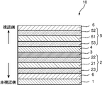
- FIG. 1 is a schematic cross-sectional view of an example of the liquid crystal display device of the present invention
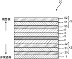
- FIG. 2 is a schematic cross-sectional view of another example of the liquid crystal display device of the present invention.
- the liquid crystal display device 10 of the present invention includes a non-white light source 1, a rear side polarizing plate 2 including a rear side polarizer 21 and a rear side optical film 22, a liquid crystal cell 3, and quantum dot fine particles.
- the light conversion layer 4 which is a color filter containing, and the front side polarizing plate 5 including the front side optical film 53 and the front side polarizer 51 are included in this order.
- the liquid crystal display device 10 having such a polarizing plate arrangement is called an in-cell type.
- the liquid crystal display device 10 of the present invention is not limited to the one in the stacking order shown in FIG. 1, and may be the out-cell type liquid crystal display device 20 shown in FIG. 2 is different from the liquid crystal display device 10 shown in FIG. 1 in that both the rear-side polarizing plate 2 and the front-side polarizing plate 5 are arranged outside the pair of cell substrates 6.
- the other configuration is the same as that shown in FIG.
- the liquid crystal display device of the present invention is not limited to the form shown in FIGS.
- the rear side polarizing plate 2 may be arranged outside the pair of cell substrates 6 and the front side polarizing plate 5 may be arranged inside the pair of cell substrates 6.
- the front-side polarizing plate 5 may be disposed outside the pair of cell substrates 6 by being disposed inside the cell substrate 6.
- a cell substrate 6 is provided between the non-white light source 1 and the rear polarizing plate 2, and the cell substrate 6 is provided on the viewing side of the front polarizing plate 5.
- a glass substrate, a plastic substrate or the like can be used, and among these, a glass substrate is preferably used.
- a “rear side” is attached to a component located closer to the non-white light source 1 than the liquid crystal cell 3, and a “front” is attached to a component located closer to the non-white light source 1 than the liquid crystal cell 3.
- the upper direction of the liquid crystal display device 10 shown in FIG. 1 may be described as “viewing side”, and the lower direction, which is the opposite direction, may be described as “non-viewing side”.
- the light conversion layer 4 is provided on the viewing side of the liquid crystal cell 3
- the rear polarizing plate 2 is provided on the non-viewing side of the liquid crystal cell 3.
- the thickness direction retardation Rth (2) of the front side optical film 53 is ⁇ 10 nm or more and 10 nm or less
- the thickness direction retardation Rth (1) of the rear side optical film 22 is The sum of Rth (2) is 200 nm or more and 300 nm or less. Below, each part which comprises the liquid crystal display device 10 is demonstrated.
- the non-white light source 1 is not particularly limited as long as it is a light source that emits non-white light.
- a cold cathode fluorescent lamp, a xenon fluorescent lamp, an LED, an organic EL, or the like can be used.
- Examples of non-white light emitted from the non-white light source 1 include monochromatic light of blue light, red light, and green light, ultraviolet light, infrared light, and the like.
- the non-white light source 1 preferably emits monochromatic light of blue light, red light, and green light, and preferably emits blue light.
- the blue light emitted from the non-white light source 1 has high energy and can easily convert the wavelength in the light conversion layer 4 described later.
- the non-white light source 1 may constitute a backlight unit together with a plurality of members such as a light guide plate, a diffusion plate, and a light collecting plate that introduce non-white light emitted from the light source from the end face.
- members constituting such a backlight unit include, for example, the latest technology of liquid crystal display device constituent materials, supervised by Iimura Yasufumi, CM Publishing, chapter 3, “Backlight technology for liquid crystal display devices, supervised by Kalantal Khalil. , CMC Publishing, etc. can be used.
- the rear side polarizing plate 2 and the front side polarizing plate 5 are configured by attaching an optical film to at least one surface of the rear side polarizer 21 and the front side polarizer 51.
- the rear-side polarizing plate 2 is provided in contact with the rear side of the liquid crystal cell 3, and a rear-side polarizer 21 and a rear-side optical film 22 formed on the viewing side of the rear-side polarizer 21,
- the rear side protective film 23 is formed on the non-viewing side of the rear side polarizer 21.
- the front polarizing plate 5 is provided in contact with the front side of the light conversion layer 4, and includes a front side polarizer 51, a front side protective film 52 formed on the viewing side of the front side polarizer 51, and a front side polarizer. And a front side optical film 53 formed on the non-viewing side of 51.
- the positional relationship between the rear side optical film 22 and the rear side protective film 23 shown in FIG. 1 may be reversed.
- the rear side optical film 22 may be formed on the viewing side of the rear side polarizer 21.
- the rear side protective film 23 may be disposed between the rear side polarizer 21 and the cell substrate 6.
- the positional relationship between the front side optical film 53 and the front side protective film 52 may be reversed, and the front side optical film 53 may be formed on the viewing side of the front side polarizer 51.
- the front side protective film 52 may be disposed between the front side polarizer 51 and the cell substrate 6.
- polarizing plates can be produced by a general method. It is preferable that the surface of the optical film in contact with the polarizer is alkali saponified and bonded to at least one surface of a polarizer produced by immersion and drawing in an iodine solution using a completely saponified polyvinyl alcohol aqueous solution. Below, each part which comprises the rear side polarizing plate 2 and the front side polarizing plate 5 is demonstrated.
- the rear side protective film 23 and the front side protective film 52 are bonded to the rear side polarizer 21 and the front side polarizer 51, respectively.
- a commercially available cellulose ester film can be used as the rear side protective film 23 and the front side protective film 52.
- Examples of commercially available cellulose ester films include Konica Minoltac Films KC8UY, KC4UY, KC8UA, KC6UA, KC4UA, KC2UA, KC4CT1, KC2CT1, KC2UAW-HC, KC4UAW-HC (manufactured by Konica Minolta, Inc.) Preferably used.
- the rear side protective film 23 and the front side protective film 52 can be omitted.
- the rear side protective film 23 is omitted, the rear side polarizer 21 is arranged so as to be in contact with the cell substrate 6.
- the front side protective film 52 is omitted, the front side polarizer 51 is disposed in contact with the cell substrate 6.
- the rear-side polarizer 21 and the front-side polarizer 51 a general polarizer used in a conventionally known liquid crystal display device can be used.
- the front polarizer 51 is preferably a monochromatic polarizer corresponding to the light source wavelength of the non-white light source 1 described above, and both the rear polarizer 21 and the front polarizer 51 are light sources of the non-white light source 1. It is more preferable that the monochromatic polarizer corresponds to the wavelength.
- the front polarizer 51 can be thinned, and the entire liquid crystal display device 10 can be thinned.
- the rear side polarizer 21 and the front side polarizer 51 may be collectively referred to as a “polarizer”.
- the “monochromatic polarizer corresponding to the light source wavelength of the non-white light source” means a polarizer capable of polarizing non-white light emitted from the non-white light source into linearly polarized light with a high degree of polarization of 95% or more.
- the monochromatic polarizer absorbs the diagonal component of the polarization axis (transmission axis) of the polarizer and transmits blue linearly polarized light with a high degree of polarization. Become a child.
- the polarizer is preferably a dichroic organic dye polarizer, a wire grid polarizer, or a cholesteric liquid crystal polarizer. Thermal stability can be improved by using such a polarizer.
- the polarizer is more preferably a dichroic organic dye polarizer. Since the dichroic organic dye polarizer can be formed by coating, an in-cell type polarizer can be easily produced.
- the thickness direction retardation Rth (2) of the front side optical film 53 is -10 nm or more and 10 nm or less, the thickness direction retardation Rth (1) of the rear side optical film 22 and the Rth (2). Is the sum of 200 nm to 300 nm. In other words, a zero retardation film is used for the front optical film 53 and a high retardation film is used for the rear optical film 22.
- the thickness direction retardation Rth (1) of the rear side optical film 22 is set to 190 nm or more and 310 nm or less.
- the light emitted from the non-white light source 1 is phase-converted by the rear side optical film 22 before reaching the light conversion layer 4, and the light absorption in the color filter of the light conversion layer 4 can be reduced, and the color filter generates heat. Can be suppressed. By suppressing this heat generation, it is possible to suppress a change in the dispersion state of the quantum dot fine particles and to suppress a decrease in color reproducibility of the liquid crystal display device.
- the thickness direction retardation Rth (1) of the rear side optical film 22 is preferably 200 nm or more and 280 nm or less, and more preferably 220 nm or more and 260 nm or less. .
- the thickness direction retardation Rth (2) of the front optical film 53 is set to ⁇ 10 nm or more and 10 nm or less, the light transmitted through the light conversion layer 4 is directly converted to the outside without being wavelength-converted by the front optical film 53. Even when the liquid crystal cell is set to the VA mode by setting the sum of the retardation Rth (1) in the thickness direction of the rear optical film 22 and the Rth (2) to 200 nm to 300 nm. Coloring of light emitted from the liquid crystal display device can be suppressed.
- the thickness direction retardations Rth (1) and Rth (2) of the rear side optical film 22 and the front side optical film 53 are represented by the following formulas (I) and (II), for example, the following method Can be obtained.
- the front side optical film and the rear side optical film are collectively referred to as “optical film”.
- R0 in Formula (I) means the phase difference of the in-plane direction of each optical film.
- Formula (I) R0 (n x -n y) ⁇ d
- Formula (II) Rth ⁇ (n x + n y ) / 2 ⁇ n z ⁇ ⁇ d
- N x the slow axis direction of the refractive index of the optical film plane
- n y the optical film plane, the refractive index in the direction perpendicular to the slow axis
- n z refractive index of the optical film in the thickness direction
- D optical film thickness (nm))
- the slow axis in the optical film plane is the tilt axis (if there is no slow axis, the arbitrary direction in the optical film plane is the tilt axis), the optical A retardation value R ( ⁇ ) is measured when light having a measurement wavelength of 550 nm is incident from an angle ⁇ with respect to the normal of the film surface.
- the retardation value R ( ⁇ ) is measured at a total of 6 points every 10 ° in the range of 0 ° to 50 °.
- the retardation Rth in the thickness direction of the optical film can be adjusted by, for example, stretching conditions and the film thickness of the optical film.
- Rth for example, both the stretching ratio in the width direction (TD direction) and the stretching ratio in the transport direction (MD direction) may be increased, or the film thickness of the optical film may be increased.
- the front side optical film 53 and the rear side optical film 22 a film made of a known polymer that has been conventionally used can be used. Specifically, a cellulose polymer film, a (meth) acrylic polymer film, a cycloolefin polymer film, a cellulose acylate film, and a polymer film composed of a mixture thereof can be used.
- the rear optical film 22 is preferably a cycloolefin polymer film or a cellulose acylate film, more preferably a cycloolefin polymer film or a cellulose acylate propionate film.
- the front side optical film 53 is preferably a cellulose acylate film, and is preferably a triacetyl cellulose film.
- the thickness direction retardation Rth (1) and Rth (2) of each optical film can be easily adjusted to a desired value.
- the thickness direction retardation of each optical film can be changed depending on the material constituting the optical film, and can also be adjusted as appropriate depending on the additive added to the optical film.
- the additive herein is preferably a pyrazole compound or a pyrimidine compound described later.
- the rear side optical film 22 and the front side optical film 53 are preferably cellulose resin films, and more preferably cellulose lower fatty acid esters.
- the “lower fatty acid” in the “lower fatty acid ester of cellulose” means a fatty acid having 6 or less carbon atoms.
- Specific examples of the cellulose resin are described in, for example, cellulose acetate, cellulose propionate, cellulose acetate butyrate, JP-A-10-45804, 08-231761, U.S. Pat. No. 2,190,052 and the like.
- Mixed fatty acid esters such as cellulose acetate propionate and cellulose acetate butyrate can be used.
- the lower fatty acid esters of cellulose particularly preferably used are cellulose triacetate and cellulose acetate propionate. These cellulose esters can be used alone or in combination.
- the cellulose resin is preferably a cellulose resin that simultaneously satisfies the following formulas (I) and (II) when the substitution degree of the acetyl group is X and the substitution degree of the propionyl group or butyryl group is Y.
- the portion not substituted with an acyl group is present as a hydroxy group.
- These can be synthesized by known methods.
- the method for measuring the substitution degree of the acyl group can be measured according to ASTM-D817-96.
- the molecular weight of the cellulose resin is preferably 60000-300000, more preferably 70000-200000 in terms of number average molecular weight (Mn).
- the cellulose resin used for the optical film preferably has a weight average molecular weight (Mw) / number average molecular weight (Mn) ratio of 4.0 or less, more preferably 1.4 to 2.3.
- Mw weight average molecular weight
- Mn number average molecular weight
- a cellulose ester synthesized using cotton linter, wood pulp, kenaf or the like as a raw material can be used alone or in combination.
- a cellulose ester synthesized from cotton linter hereinafter sometimes simply referred to as linter
- linter a cellulose ester synthesized from cotton linter
- the cycloolefin polymer constituting the optical film is a polymer resin containing an alicyclic structure.
- a preferred cycloolefin polymer is a resin obtained by polymerizing or copolymerizing a cyclic olefin.
- cyclic olefin examples include norbornene, dicyclopentadiene, tetracyclododecene, ethyltetracyclododecene, ethylidenetetracyclododecene, tetracyclo [7.4.0.110, 13.02,7] trideca-2,4, Unsaturated hydrocarbons with polycyclic structures such as 6,11-tetraene and derivatives thereof; cyclobutene, cyclopentene, cyclohexene, 3,4-dimethylcyclopentene, 3-methylcyclohexene, 2- (2-methylbutyl) -1-cyclohexene, cyclo Examples thereof include monocyclic unsaturated hydrocarbons such as octene, 3a, 5,6,7a-tetrahydro-4,7-methano-1H-indene, cycloheptene, cyclopentadiene, cyclohexa
- cyclic olefins may have a polar group as a substituent.
- the polar group include a hydroxy group, a carboxy group, an alkoxyl group, an epoxy group, a glycidyl group, an oxycarbonyl group, a carbonyl group, an amino group, an ester group, and a carboxylic acid anhydride group. Or a carboxylic anhydride group is preferred.
- the cycloolefin polymer is preferably an addition copolymerized monomer other than the cyclic olefin.
- Addition copolymerizable monomers include ethylene or ⁇ -olefins such as ethylene, propylene, 1-butene and 1-pentene; 1,4-hexadiene, 4-methyl-1,4-hexadiene, 5-methyl- And dienes such as 1,4-hexadiene and 1,7-octadiene.
- the cycloolefin resin is obtained by an addition polymerization reaction or a metathesis ring-opening polymerization reaction. These polymerization reactions are performed in the presence of a catalyst.
- the addition polymerization catalyst include a polymerization catalyst composed of a vanadium compound and an organoaluminum compound.
- a polymerization catalyst comprising a metal halide such as ruthenium, rhodium, palladium, osmium, iridium, platinum, nitrate or acetylacetone compound and a reducing agent; or titanium, vanadium, zirconium, tungsten, molybdenum Examples thereof include a polymerization catalyst comprising a metal halide such as acetylacetone compound and an organoaluminum compound.
- the polymerization temperature, pressure and the like are not particularly limited, but the polymerization is usually carried out at a polymerization temperature of ⁇ 50 to 100 ° C. and a polymerization pressure of 0 to 490 N / cm 2 .
- the cycloolefin polymer is preferably a polymer obtained by polymerizing or copolymerizing a cyclic olefin, followed by a hydrogenation reaction to change the unsaturated bond in the molecule to a saturated bond.
- the hydrogenation reaction is performed by blowing hydrogen in the presence of a known hydrogenation catalyst.
- Hydrogenation catalysts include transition metal compounds such as cobalt acetate / triethylaluminum, nickel acetylacetonate / triisobutylaluminum, titanocene dichloride / n-butyllithium, zirconocene dichloride / sec-butyllithium, tetrabutoxytitanate / dimethylmagnesium / alkyl Homogeneous catalyst composed of a combination of metal compounds; heterogeneous metal catalyst such as nickel, palladium, platinum; nickel / silica, nickel / diatomaceous earth, nickel / alumina, palladium / carbon, palladium / silica, palladium / diatomaceous earth And a heterogeneous solid-supported catalyst in which a metal catalyst such as palladium / alumina is supported on a carrier.
- transition metal compounds such as cobalt acetate / triethylaluminum, nickel acetylacet
- Norbornene resin may be used as the cycloolefin polymer.
- the norbornene-based resin preferably has a norbornene skeleton as a repeating unit. Specific examples thereof include, for example, JP-A-62-252406, JP-A-62-2252407, JP-A-2-133413, JP-A-63-145324, JP-A-63-264626.
- ZEONEX, ZEONOR manufactured by Nippon Zeon Co., Ltd., Arton manufactured by JSR Corporation, APPEL manufactured by Mitsui Chemicals, Inc. (APL8008T, APL6509T, APL6013T, APL5014DP, APL6015T) and the like are preferably used.
- the molecular weight of the cycloolefin polymer is appropriately selected according to the purpose of use, but it is calculated in terms of polyisoprene or polystyrene measured by gel permeation chromatography method of cyclohexane solution (toluene solution if the polymer resin does not dissolve).
- the weight average molecular weight is preferably 5,000 to 500,000, more preferably 8,000 to 200,000, and still more preferably 10,000 to 100,000. At this time, the mechanical strength and molding processability of the molded body are highly balanced.
- the optical film may be appropriately mixed with polymer components other than cellulose ester.
- the polymer component to be mixed is preferably excellent in compatibility with the cellulose ester, and the transmittance when forming an optical film is preferably 80% or more, more preferably 90% or more, and still more preferably 92% or more. It is.
- Additives added to the dope include plasticizers, ultraviolet absorbers, retardation adjusting agents, antioxidants, deterioration inhibitors, peeling aids, surfactants, dyes, fine particles, and the like.
- additives other than the fine particles may be added during the preparation of the cellulose ester solution, or may be added during the preparation of the fine particle dispersion.
- plasticizers, antioxidants, ultraviolet absorbers and the like that impart heat and moisture resistance.
- These compounds are preferably contained in an amount of 1 to 30% by mass, preferably 1 to 20% by mass, based on the cellulose ester. In order to suppress bleeding out during stretching and drying, a compound having a vapor pressure at 200 ° C. of 1400 Pa or less is preferable.
- the rear side optical film 22 and the front side optical film 53 have a cellulose ester and a substituent selected from a carboxyl group, a hydroxyl group, an amino group, an amide group, and a sulfonic acid group and have a weight average molecular weight of 500 to 200. It is preferable to contain a polymer or oligomer of a vinyl compound that is 1,000. The mass ratio of the content of the cellulose ester and the polymer or oligomer is preferably 95: 5 to 50:50.
- the compound added to adjust the retardation of the optical film may be an aromatic compound having two or more aromatic rings as described in EP 911,656A2. . Two or more aromatic compounds may be used in combination.
- the aromatic ring of the aromatic compound includes an aromatic heterocyclic ring in addition to the aromatic hydrocarbon ring.
- the aromatic ring is particularly preferably an aromatic heterocycle.
- the aromatic heterocyclic ring is generally an unsaturated heterocyclic ring, and a 1,3,5-triazine ring is particularly preferable.
- the retardation adjusting agent it is preferable to use an organic additive having a structure represented by the following general formula (1). Thereby, the glass transition temperature of the surface of a front side optical film and a rear side optical film can be reduced, and blocking resistance can be improved.
- Ar 1 to Ar 3 in the above formula (1) each independently represents a substituted or unsubstituted aromatic hydrocarbon ring or nitrogen-containing aromatic heterocyclic ring.
- X 1 and Y 1 each independently represents a substituted or unsubstituted nitrogen-containing aromatic heterocyclic ring.
- the ring constituent atoms of the aromatic hydrocarbon ring or nitrogen-containing aromatic heterocycle represented by Ar 1 and Ar 3 are the ring structures of the aromatic hydrocarbon ring or nitrogen-containing aromatic heterocyclic ring other than X 1 and Y 1 , respectively. It is not directly bonded to the atom.
- X 1 and Y 1 and Ar 1 ⁇ Ar 3 is preferably a pyrazole compound containing a pyrazole ring .
- Ar 1 to Ar 3 each independently represents a substituted or unsubstituted aromatic hydrocarbon ring or nitrogen-containing aromatic heterocyclic ring.
- Ar 1 to Ar 3 are each independently an alkyl group (methyl group, ethyl group, n-propyl group, isopropyl group, tert-butyl group, n-octyl group). , 2-ethylhexyl group, etc.), a cycloalkyl group (cyclohexyl group, cyclopentyl group, 4-n-dodecylcyclohexyl group, etc.), an aromatic hydrocarbon ring or an aromatic heterocyclic ring.
- an aromatic hydrocarbon ring or an aromatic heterocycle is preferable, and a 5-membered or 6-membered aromatic hydrocarbon ring or an aromatic heterocycle is particularly preferable.
- the structure of the 5-membered or 6-membered aromatic hydrocarbon ring or aromatic heterocyclic ring is not limited.
- the 5-membered or 6-membered aromatic hydrocarbon ring or aromatic heterocyclic ring represented by Ar 1 to Ar 3 may have a substituent.
- substituents include a halogen atom (fluorine atom, chlorine atom, bromine atom, iodine atom, etc.), alkyl group (methyl group, ethyl group, n-propyl group, isopropyl group, tert-butyl group, n-octyl group).
- Aryloxy group phenoxy group, 2-methylphenoxy group, 4-tert-butylphenoxy group) , 3-nitrophenoxy group, 2-tetradecanoylaminophenoxy group, etc.
- acyloxy group formyloxy group, acetyloxy group, pivaloyloxy group, stearoyloxy group, benzoyloxy group, p-methoxyphenylcarbonyloxy group, etc.
- Amino group (amino group, methylamino group, dimethylamino group, anilino group, N-methyl-anilino group, diphenylamino group, etc.)
- acylamino group formylamino group, acetylamino group, pivaloylamino group, lauroylamino group, benzoylamino) Group
- alkyl and arylsulfonylamino groups methylsulfonylamino group, butylsulfonylamino
- aromatic hydrocarbon rings or nitrogen-containing aromatic heterocycles represented by Ar 1 and Ar 3 represent aromatic hydrocarbon rings or nitrogen-containing aromatics other than X 1 and Y 1 , respectively. It is not directly bonded to the ring atoms of the heterocycle.
- Ar 1 to Ar 3 represent a benzene ring, a pyrrole ring, a pyrazole ring, an imidazole ring, a 1,2,3-triazole ring, or a 1,2,4-triazole ring. This is preferable because an optical film having excellent property variation effects and excellent durability can be obtained.
- X 1 and Y 1 each independently represent a substituted or unsubstituted nitrogen-containing aromatic heterocycle.
- the substituted or unsubstituted nitrogen-containing aromatic heterocycle include, for example, each independently a pyrrole ring, pyrazole ring, imidazole ring, 1,2,3-triazole ring or 1,2,4-triazole ring.
- a substituted or unsubstituted imidazole ring, pyrazole ring or triazole ring is preferable because a film with more excellent blocking resistance can be obtained, and a pyrazole ring is particularly preferable.
- the pyrazole ring, 1,2,3-triazole ring, 1,2,4-triazole ring and imidazole ring represented by X 1 and Y 1 may be tautomers. Specific structures of the pyrrole ring, pyrazole ring, imidazole ring, 1,2,3-triazole ring or 1,2,4-triazole ring are shown below.
- R 5 represents a hydrogen atom or a non-aromatic substituent.
- the non-aromatic substituent represented by R 5 include the same groups as the non-aromatic substituent among the substituents that Ar 1 to Ar 3 may have in the general formula (1).
- R 5 is preferably a hydrogen atom, an alkyl group having 1 to 5 carbon atoms or an acyl group having 1 to 5 carbon atoms, and particularly preferably a hydrogen atom.
- X 1 and Y 1 may have a substituent, and the substituent may include Ar 1 to Ar 3 in the general formula (1).
- the same group as a good substituent can be mentioned.
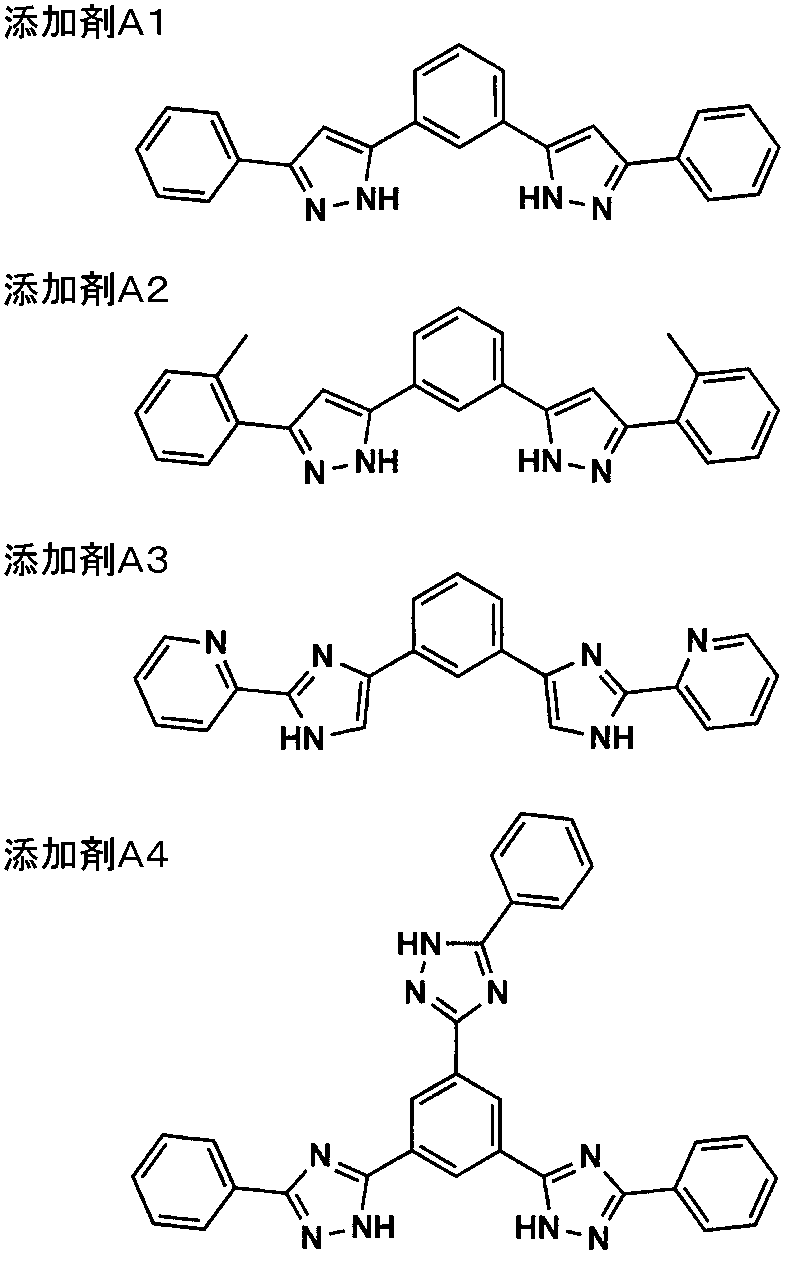
- Specific examples of the compound having the structure represented by the general formula (1) include the following compounds (additives A1 to A4), but are not limited thereto, and examples thereof include those disclosed in JP2013-24903A. Those described in paragraphs 0051 to 0064 can be preferably used.
- the content of the organic additive is 0.5 to 10% by mass with respect to the total amount of the resin.
- content of an organic additive means the organic additive which has a structure represented by General formula (1), and organic additives other than the organic additive which has a structure represented by General formula (1). It is content with respect to the whole quantity of the polymer which comprises the optical film of the included organic additive.
- the organic additive has a solubility in dichloromethane at 23 ° C. of 0.01 to 1.00% by mass, and the organic additive has a solubility in ethanol at 23 ° C. of 2.00 to 10.00% by mass. It is preferable from the viewpoint of effect expression. If the solubility with respect to a dichloromethane is 0.01 mass% or more, the internal haze of an optical film will become more favorable. If it is 1.00 mass% or less, blocking tolerance will become more favorable. The expression of such an effect is presumed to be because the organic additive is more easily localized on both surfaces of the optical film by satisfying the above range.
- the organic additive preferably has a solubility in ethanol at 23 ° C. of 2.0% by mass or more because the internal haze of the optical film becomes better. It is preferable that the organic additive has a solubility in ethanol at 23 ° C. of 10.00% by mass or less because the blocking resistance becomes better. The expression of such an effect is presumed to be because the organic additive is easily localized on the surface of the optical film by satisfying the above range.
- the said organic additive when manufacturing an optical film, may be used in the form melt
- the solubility within a range where the effects of the invention can be obtained is preferably, for example, dissolved in a 20:80 solvent in a mass mixing ratio of dichloromethane and ethanol at a ratio of 0.001 to 6.00 mass%.
- the solvent when the solvent has a mass mixing ratio of 50:50, the solvent is preferably dissolved at a ratio of 0.001 to 8.00% by mass.
- solubility is more than the lower limit (0.001 mass%) of the said range, since it is easy to obtain the quality calculated
- liquid crystal cell 3 a liquid crystal cell used in a normal liquid crystal display device can be used as appropriate, and for example, VA or IPS can be used.
- the liquid crystal cell 3 is preferably a layer formed by filling a nematic liquid crystal material having positive dielectric anisotropy.
- the liquid crystal cell 3 is in a VA mode or an IPS mode.
- a VA mode liquid crystal cell rod-like liquid crystal molecules are aligned substantially vertically when no voltage is applied.
- rod-like liquid crystal molecules are aligned substantially parallel to the substrate, and the liquid crystal molecules respond in a planar manner when an electric field parallel to the substrate surface is applied.
- the IPS mode displays black when no electric field is applied, and the absorption axes of the pair of upper and lower polarizing plates are orthogonal.
- the light conversion layer 4 is composed of a color filter containing quantum dot fine particles, and is a layer that is provided on the viewing side of the liquid crystal cell 3 and that can convert the wavelength of light transmitted through the liquid crystal cell 3.
- the color filter has a structure in which red, green, and blue dot-like images are arranged in a matrix and the boundary is divided by a dark color separation wall such as a black matrix.
- This color filter contains at least quantum dot fine particles.
- the quantum dot fine particles are inorganic nano-semiconductor particles having a predetermined size having a quantum confinement effect.
- the quantum dot fine particles are composed of a phosphor that is excited by light transmitted through the front-side polarizer and emits visible light (blue light, red light, and green light) on a longer wavelength side than this light.
- the Examples of the phosphor constituting these quantum dot fine particles include zinc silicate (ZnSiO 3 ), cadmium silicate (CdSiO 3 ), and cadmium borate (Cd 2 B 2 O 5 ).
- respective quantum dot fine particles corresponding to blue light, red light and green light are dispersed.
- the light transmitted from the front polarizer can be converted into white light in which blue light, red light and green light are mixed.
- the light conversion layer 4 may contain either one or both of a pigment and a dye in addition to the quantum dot fine particles.
- examples of the pigment or dye contained in the light conversion layer 4 include those described in JP-A-2009-139616.
- a method for producing such a light conversion layer 4 a conventionally known method for producing a color filter can be used. Specifically, a dyeing method, a printing method, a colored resist method, a transfer method, an ink jet method, a printing method can be used. Etc.
- the light emitted from the non-white light source 1 passes through the rear optical film 22 before reaching the light conversion layer 4, so that the phase difference of the light reaching the light conversion layer 4 is reduced.
- the rear side optical film 22 is adjusted. Thereby, heat generation in the color filter constituting the light conversion layer 4 can be suppressed, and fluctuations in the dispersion state of the quantum dot fine particles dispersed in the light conversion layer 4 can be prevented. Thereby, the fall of the color reproducibility of a liquid crystal display device can be suppressed.
- One aspect of the present invention includes a non-white light source, a rear-side polarizing plate including a rear-side polarizer and a rear-side optical film, a liquid crystal cell, a light conversion layer that is a color filter containing quantum dot fine particles, and a front side.
- An optical film and a front-side polarizing plate including a front-side polarizer, and a retardation Rth (2) in the thickness direction of the front-side optical film is from ⁇ 10 nm to 10 nm.
- the sum of the thickness direction retardation Rth (1) and the Rth (2) is 200 nm or more and 300 nm or less.
- the rear optical film preferably contains a pyrazole compound.
- the liquid crystal cell is preferably in VA mode or IPS mode.
- the thickness direction retardation Rth (1) of the rear side optical film is preferably 200 nm or more and 280 nm or less.
- Another aspect of the present invention is a non-white light source, a rear-side polarizing plate including a rear-side polarizer and a rear-side optical film, a liquid crystal cell, and a light conversion layer that is a color filter containing quantum dot fine particles
- the liquid crystal display device includes a front side optical film and a front side polarizing plate including a front side polarizer in this order, and one of the pair of optical films is used as the front side optical film.
- the thickness direction retardation Rth (2) is ⁇ 10 nm or more and 10 nm or less, and the other of the pair of optical films is used as the rear side optical film, and the thickness direction retardation Rth (1)
- the sum of Rth (2) is a pair of optical films that are 200 nm or more and 300 nm or less.
- the present invention it is possible to provide a liquid crystal display device in which color reproducibility is unlikely to deteriorate and a pair of optical films used in the liquid crystal display device.
- Example 1 Preparation of rear side optical film>
- CAP cellulose acetate propionate
- a silica compound product name: Aerosil R812 (manufactured by Nippon Aerosil Co., Ltd.)
- the main dope for producing the rear side optical film of Example 1 was prepared by the following procedure. First, 250 parts by mass of methylene chloride (dichloromethane) and 50 parts by mass of ethanol were charged into a pressure dissolution tank, and the mixture was stirred and mixed while heating. In this pressure dissolution tank, 100 parts by mass of cellulose acetate propionate (CAP) was added while stirring the mixed solution in the tank. The liquid mixture in the pressure dissolution tank was heated and stirred to completely dissolve CAP. This solution of CAP was used as Azumi Filter Paper No. Filtered using 244.
- a fine particle additive solution made of a silica compound prepared in advance as follows was used.
- a fine particle dispersion composed of a silica-based compound was prepared using ethanol, and this fine particle dispersion was put into a dissolution tank containing methylene chloride and sufficiently stirred and filtered to prepare a predetermined fine particle addition liquid.
- fine particles made of 11 parts by mass of a silica-based compound product name: Aerosil R812 (manufactured by Nippon Aerosil Co., Ltd.)
- 89 parts by mass of ethanol are stirred and mixed with a dissolver for 50 minutes, and then with Manton Gorin.
- a fine particle dispersion was obtained by dispersing.
- the main dope prepared as described above was cast on a stainless belt support to obtain a dope film (web).
- the solvent was evaporated on a stainless steel belt support until the amount of residual solvent in the cast web was 75%.
- the web was peeled from the stainless steel belt support with a peeling tension of 130 N / m to obtain a resin film.
- the peeled resin film was stretched 30% in the width direction using a tenter while applying heat at 150 ° C.
- the amount of residual solvent in the resin film at the start of stretching was 15%.
- Example 1 drying was terminated by passing the resin film through a drying zone while being conveyed by a number of rollers.
- the drying temperature was 130 ° C. and the transport tension was 100 N / m.
- the rear side optical film used in Example 1 was obtained as described above.
- the rear optical film had a dry film thickness of 92 ⁇ m and a thickness direction retardation Rth (1) of 240 nm.
- Example 2 a rear side optical film was produced in the same manner as in Example 1 except that the following pyrimidine compound was used instead of the pyrazole compound used in the production of the rear side optical film of Example 1. .
- Example 6 and 7 and Comparative Examples 1 and 3 the rear side optical film produced in Example 1 was used.
- Examples 3 and 4 and Comparative Examples 2 and 4 are different from Example 1 except that the thickness of the rear side optical film is changed to the value shown in the column of “film thickness” in Table 1, respectively.
- a rear side optical film was prepared in the same manner as in Example 1. With this change in the film thickness, the thickness direction retardation of the rear side optical film became the value shown in the column of “Thickness direction retardation Rth (1)” in Table 1.
- Example 5 a rear-side optical film was produced in which cycloolefin polymer (COP) was used as a resin base material, and the resin base material had a thickness of 100 ⁇ m.
- the rear side optical film used in Example 5 was produced as follows.
- thermoplastic norbornene resin constituting the COP film was produced. Under nitrogen atmosphere, 500 parts of dehydrated cyclohexane was mixed with 0.82 part of 1-hexene, 0.15 part of dibutyl ether and 0.30 part of triisobutylaluminum in a reactor at room temperature.
- the above ring-opening polymer was removed from the reaction solution while removing the cyclohexane and other volatile components as a solvent at a temperature of 270 ° C. and a pressure of 1 kPa or less using a cylindrical concentration dryer (manufactured by Hitachi, Ltd.).
- the hydrogenated polymer was extruded in the form of a strand from the extruder in the molten state.
- the polymer after the extrusion was cooled and then pelletized and recovered.
- the ring-opened polymer hydrogenated product (thermoplastic norbornene resin) had a weight average molecular weight (Mw) of 35,000, a hydrogenation rate of 99.9%, and a glass transition temperature (Tg) of 136 ° C. .
- the pellets of the thermoplastic norbornene resin were dried at 70 ° C. for 2 hours using a hot air dryer in which air was circulated to remove moisture.
- the pellets were extruded into a sheet using a T-die type film melt extruder at a temperature of 260 ° C. and a die temperature of 260 ° C.
- the extruded sheet-shaped thermoplastic norbornene-based resin is cooled by passing it through three cooling drums (diameter 300 mm, drum temperature 100 ° C., take-off speed 0.35 m / s), and a raw material having a thickness of 200 ⁇ m and a width of 300 mm A film was obtained.
- the obtained raw film had a volatile component content of 0.01% by weight and a saturated water absorption of 0.01% by weight.
- the thickness variation of the raw film was ⁇ 1.2% of the thickness in the width direction and ⁇ 1.1% in the longitudinal direction.
- the resin melt kneader used was equipped with a 65 mm ⁇ diameter screw provided with a leaf disk-shaped polymer filter (filtration accuracy 30 ⁇ m).
- the raw film obtained above is oven temperature (preheating temperature, stretching temperature, heat setting temperature) 136 ° C., film feeding speed 1 m / min, and chuck movement accuracy within ⁇ 1%.
- the rear side optical film used in Example 5 was obtained by performing simultaneous biaxial stretching at 1.41 times the longitudinal stretching ratio and 1.50 times the lateral stretching ratio. This rear optical film had a thickness of 100 ⁇ m and Rth (1) 290 nm.
- a main dope having the following composition was prepared. That is, first, methylene chloride and ethanol were charged as solvents in a pressure dissolution tank. Then, a cellulose acylate, a sugar ester, an ester compound, and a mat material dispersion are charged into a pressurized dissolution tank containing the solvent while stirring the solvent, and the mixed liquid is heated and stirred to cellulose acylate. Etc. were completely dissolved.
- Cellulose acylate 100 parts by weight Sugar ester T1 12 parts by weight Ester compound E1 4 parts by weight Matting agent: 12% ethanol dispersion of R812 (manufactured by Nippon Aerosil Co., Ltd.) 1.4 parts by mass Methylene chloride 430 parts by mass Ethanol 40 parts by mass
- the main dope was prepared by filtration using 244.
- Cellulose acylate Cellulose triacetate (TAC) having a number average molecular weight of 70,000 having an acetyl group substitution degree of 2.80
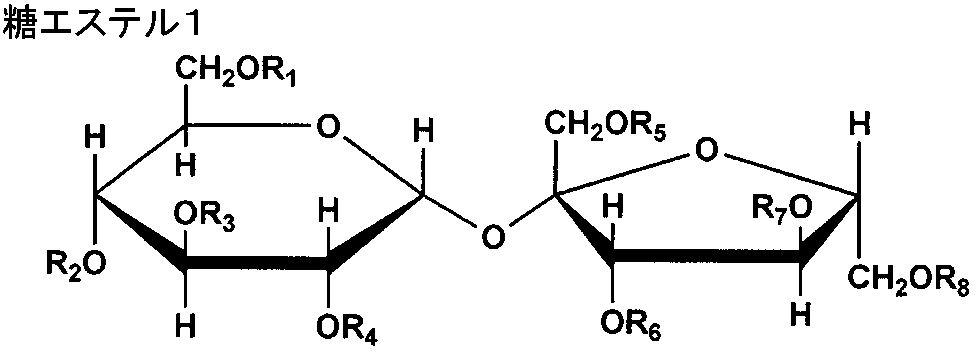
- Sugar ester T1 Sugar ester represented by the following chemical formula (In the formula, R 1 to R 8 are acetyl groups.)
- Ester compound E1 251 g of 1,2-propylene glycol, 278 g of phthalic anhydride, 91 g of adipic acid, 610 g of benzoic acid, 0.191 g of tetraisopropyl titanate as an esterification catalyst, 2 L equipped with a thermometer, stirrer and slow cooling tube The four-necked flask was charged. These mixtures were gradually heated while being stirred in a nitrogen stream until reaching 230 ° C. The ester compound E1 was obtained by carrying out dehydration condensation reaction for 15 hours, and distilling off unreacted 1,2-propylene glycol under reduced pressure at 200 ° C. after completion of the reaction. This ester compound E1 had an acid value of 0.10 and a number average molecular weight of 450.
- the main dope prepared above was uniformly cast on a stainless steel band support at a temperature of 22 ° C. and a width of 1.8 m using a belt casting apparatus to obtain a dope film (web).
- the solvent was evaporated until the residual solvent amount in the web reached 20%, and the web was peeled off from the stainless steel band support with a peeling tension of 162 N / m to obtain a resin film.
- the peeled resin film is heated to 35 ° C. to evaporate the solvent, slit to 1.6 m width, and then to the original width in the width direction (TD direction) at 160 ° C. using a tenter stretching machine.
- the film was stretched 1.1 times. When the stretching by the tenter was started, the residual solvent amount in the resin film was 4% by mass.
- the resin film was dried while being transported by a large number of rollers through a drying zone at 120 ° C. and 140 ° C., and slit to a width of 1.3 m.
- a knurling process having a width of 10 mm and a height of 2.5 ⁇ m was applied to both ends of the resin film, and then wound on a core to prepare a front side optical film.
- the film thickness of the front side optical film was 40 ⁇ m, and the winding length was 5000 m. Further, the retardation Rth (2) in the thickness direction of the front side optical film was 5 nm.
- Examples 2 to 7 and Comparative Examples 1 to 4 by changing the film thickness of the front optical film, as shown in the column of “Thickness direction retardation (2)” in Table 1 below, the front optical The thickness direction retardation Rth (2) of the film was changed. Similarly, in Examples 2 to 7 and Comparative Examples 1 to 4, by changing the film thickness of the rear side optical film, as shown in the column of “Thickness direction retardation (1)” in Table 1 below, The thickness direction retardation Rth (1) of the side optical film was changed.
- the slow axis in the optical film plane is the tilt axis (if there is no slow axis, any direction in the film plane is the tilt axis), the optical A retardation value R ( ⁇ ) was measured when light having a measurement wavelength of 550 nm was incident from an angle ⁇ with respect to the normal of the film surface.
- the retardation value R ( ⁇ ) was measured at a total of 6 points every 10 ° in the range of 0 ° to 50 °.
- the liquid crystal display devices of Examples 1 to 7 and Comparative Examples 1 to 4 in Table 1 were prepared by combining the rear side optical film and the front side optical film prepared above.
- the “in-cell” in Table 1 means an in-cell type liquid crystal display device in which the rear-side polarizing plate and the front-side polarizing plate are arranged inside the pair of cell substrates.
- the “out-cell” in Table 1 means an out-cell type liquid crystal display device in which the rear-side polarizing plate and the front-side polarizing plate are arranged outside the pair of cell substrates.
- non-viewing side shown in the “position” column of the rear side optical film in Table 1 means that the rear side optical film is arranged on the non-viewing side of the rear side polarizer.
- Viewing side in Table 1 means that the rear side optical film is arranged on the viewing side of the rear side polarizer.
- a cell substrate 6 having a transparent electrode formed on the surface of a glass substrate was prepared.
- the front-side polarizing plate 5 was bonded to the surface of the cell substrate 6 on which the transparent electrode was formed via an adhesive.
- the front-side polarizing plate 5 here was prepared as described above with respect to the front-side protective film 52 which is a Konica Minolta-tack film (product name: KC8UY) and the front-side polarizer 51 made of a dichroic organic dye polarizer. What stuck the front side optical film 53 was used.
- the front protective film 52 was in contact with the cell substrate 6.
- a black matrix was formed on the surface of the front side optical film 53 of the front side polarizing plate 5.
- a red filter containing red dot fine particles, a green filter containing green dot fine particles, and a blue filter containing blue dot fine particles were respectively formed in the corresponding accommodating space of the black matrix by a lithography process.
- the light conversion layer 4 was produced on the surface of the front side polarizing plate 5.
- FIG. 6 Another glass substrate (cell substrate 6) similar to the cell substrate 6 is prepared, and the rear side of the other cell substrate 6 on the side on which the transparent electrode is formed is provided via an adhesive.
- the polarizing plate 2 was bonded.
- the rear side polarizing plate 2 here was produced as described above with respect to the rear side protective film 23 which is a Konica Minolta-tack film (product name: KC8UY) and the rear side polarizer 21 made of a dichroic organic dye polarizer. What stuck the rear side optical film 22 was used.
- the rear protective film 23 was in contact with the cell substrate 6.
- the liquid crystal cell gap is 4.2 ⁇ m through a spacer having a uniform particle diameter of 2.8 ⁇ m, facing the surface on the rear side polarizing plate 2 side of the cell substrate 6 with the rear side polarizing plate 2 thus prepared.
- the surface of the cell substrate 6 on which the front side polarizing plate 5 was attached was fixed on the front side polarizing plate 5 side.
- a liquid crystal cell 3 was produced by dropping and injecting a liquid crystal composition (ZLI1132, manufactured by Merck & Co., Inc.) between the cell substrates 6.
- a backlight (light source: blue LED, light source peak top: 45 nm, full width at half maximum) as a non-white light source 1 on the surface opposite to the rear side polarizing plate 2 of the cell substrate 6 to which the rear side polarizing plate 2 is attached. 30 nm) was attached to produce the in-cell type liquid crystal display device of Example 1 shown in FIG.
- Example 2 to 5 and Comparative Examples 1 to 4 differ from Example 1 except that the retardations Rth (1) and Rth (2) in the thickness direction of the rear side optical film and the front side optical film are changed.
- a liquid crystal display device was produced in the same manner.
- Example 6 the out-cell type liquid crystal display device shown in FIG. 2 was produced. Specifically, first, a cell substrate 6 having a transparent electrode formed on the surface of a glass substrate was prepared. Next, a black matrix was formed on the surface of the cell substrate 6 opposite to the surface on which the transparent electrode was formed. Next, a red filter containing red dot fine particles, a green filter containing green dot fine particles, and a blue filter containing blue dot fine particles were each formed by a lithography process in the corresponding accommodation space of the black matrix. In this way, the light conversion layer 4 was produced on the surface of the cell substrate 6.
- the front side polarizing plate 5 was affixed on the surface on the opposite side to the surface in which the light conversion layer 4 of the cell substrate 6 was formed through the adhesive.
- the front-side polarizing plate 5 having the same configuration as in Example 1 was used.
- FIG. 6 Another glass substrate (cell substrate 6) similar to the cell substrate 6 is prepared, and the other cell substrate 6 is placed on the surface of the cell substrate 6 produced above on the light conversion layer 4 side.
- the liquid crystal cell gap was fixed to 4.2 ⁇ m through a spacer having a uniform particle diameter of 2.8 ⁇ m.
- a liquid crystal cell 3 was produced by dropping and injecting a liquid crystal composition (ZLI1132, manufactured by Merck) between the cell substrates 6.
- the rear-side polarizing plate 2 is bonded to the rear-side surface of the other cell substrate 6, and the backlight (light source: blue) is used as the non-white light source 1 with respect to the rear-side polarizing plate 2.
- the backlight light source: blue
- Example 7 a liquid crystal display device was produced in the same manner as in Example 1 except that the rear side optical film and the rear side protective film in the liquid crystal display device of Example 1 were replaced.
- the NTSC ratio of the liquid crystal display device of each example and each comparative example was calculated and evaluated according to the following criteria. The evaluation results are shown in the “color reproducibility” column of Table 1.
- the polar angle direction is 60 degrees from the front of the apparatus in a dark room
- the azimuth angle direction is 0 degrees
- the brightness values of black display and white display at 90 degrees and 90 degrees were measured, white brightness / black brightness were calculated, and the viewing angle characteristics of the liquid crystal display devices of the examples and comparative examples were evaluated according to the following criteria.
- the evaluation result is shown in the column of “oblique contrast” in Table 1.
- the viewing angle contrast is 50 or more, and light leakage cannot be recognized. 2: The minimum value of the viewing angle contrast is less than 50 and 25 or more, and a slight light leakage is recognized but is acceptable. 1: The minimum value of the viewing angle contrast is less than 25, and a large light leakage is recognized and is not acceptable.
- the liquid crystal display devices of Examples 1 to 7 are light conversions that are non-white light sources, rear-side polarizing plates including a rear-side polarizer and a rear-side optical film, a liquid crystal cell, and a color filter containing quantum dot fine particles.
- the sum of retardation Rth (1) in the thickness direction of the rear side optical film and Rth (2) was 200 nm or more and 300 nm or less.
- the phase of the light emitted from the non-white light source was converted by the rear side optical film. This suppresses the heat generation of the light conversion layer due to the light reaching the light conversion layer, and it becomes clear that the dispersion state of the quantum dot fine particles does not change, and it is clear that the color reproducibility is excellent, and the effect of the present invention is shown. It was.
- the liquid crystal display device of Comparative Example 4 could not obtain excellent color reproducibility due to the small retardation Rth (2) in the thickness direction of the rear side optical film.
- the reason why the color reproducibility is lowered is thought to be that the light from the non-white light source before reaching the light conversion layer cannot be sufficiently phase-converted by the rear side optical film. In other words, it is considered that the light from the non-white light source is directly incident on the light conversion layer, and the color filter constituting the light conversion layer generates heat, and the dispersion state of the quantum dot fine particles dispersed in the light conversion layer is changed. .
- the present invention it is possible to provide a liquid crystal display device in which color reproducibility is unlikely to deteriorate and a pair of optical films used in the liquid crystal display device.
Landscapes
- Physics & Mathematics (AREA)
- Nonlinear Science (AREA)
- Mathematical Physics (AREA)
- Chemical & Material Sciences (AREA)
- Crystallography & Structural Chemistry (AREA)
- General Physics & Mathematics (AREA)
- Optics & Photonics (AREA)
- Liquid Crystal (AREA)
- Polarising Elements (AREA)
Abstract
Description
図1は、本発明の液晶表示装置の一例の模式的な断面図であり、図2は、本発明の液晶表示装置の別の一例の模式的な断面図である。本発明の液晶表示装置10は、図1に示すように、非白色光源1と、リア側偏光子21およびリア側光学フィルム22を含むリア側偏光板2と、液晶セル3と、量子ドット微粒子を含有するカラーフィルタである光変換層4と、フロント側光学フィルム53およびフロント側偏光子51を含むフロント側偏光板5とをこの順に含む。
非白色光源1は、非白色光が出射される光源であれば特に限定されず、例えば、冷陰極蛍光ランプ、キセノン蛍光ランプ、LED、有機EL等を用いることができる。非白色光源1から出射される非白色光としては、例えば、青色光、赤色光および緑色光のいずれかの単色光、紫外線、赤外線等が挙げられる。これらの中でも、非白色光源1は、青色光、赤色光および緑色光のいずれかの単色光を出射することが好ましく、中でも青色光を出射することが好ましい。非白色光源1から出射される青色光は、エネルギーが高く、後述する光変換層4において、容易に波長を変換することができる。
リア側偏光板2およびフロント側偏光板5は、リア側偏光子21およびフロント側偏光子51の少なくとも一方の面に光学フィルムを貼り合わせて構成されている。具体的には、リア側偏光板2は、液晶セル3のリア側に接して設けられ、リア側偏光子21と、リア側偏光子21の視認側に形成されたリア側光学フィルム22と、リア側偏光子21の非視認側に形成されたリア側保護フィルム23とによって構成されている。フロント側偏光板5は、光変換層4のフロント側に接して設けられ、フロント側偏光子51と、フロント側偏光子51の視認側に形成されたフロント側保護フィルム52と、フロント側偏光子51の非視認側に形成されたフロント側光学フィルム53とによって構成されている。
リア側保護フィルム23およびフロント側保護フィルム52はそれぞれ、リア側偏光子21およびフロント側偏光子51に貼り合わされている。リア側保護フィルム23およびフロント側保護フィルム52としては、市販のセルロースエステルフィルムを用いることができる。市販のセルロースエステルフィルムとしては、例えば、コニカミノルタタックフィルム KC8UY、KC4UY、KC8UA、KC6UA、KC4UA、KC2UA、KC4CT1、KC2CT1、KC2UAW-H-C、KC4UAW―H-C(以上コニカミノルタ株式会社製)が好ましく用いられる。なお、液晶表示装置がインセルタイプで構成されている場合には、リア側保護フィルム23およびフロント側保護フィルム52を省略することもできる。リア側保護フィルム23を省略する場合、リア側偏光子21はセル基板6に接するように配置される。フロント側保護フィルム52を省略する場合、フロント側偏光子51はセル基板6に接するように配置される。
リア側偏光子21およびフロント側偏光子51は、従来公知の液晶表示装置に用いられる一般的な偏光子を用いることができる。フロント側偏光子51は、上述した非白色光源1の光源波長に対応した単色偏光子であることが好ましく、リア側偏光子21およびフロント側偏光子51のいずれもが、非白色光源1の光源波長に対応した単色偏光子であることがより好ましい。このような単色偏光子を用いることによりフロント側偏光子51を薄くすることができ、液晶表示装置10全体を薄型化することができる。以下において、リア側偏光子21およびフロント側偏光子51をまとめて「偏光子」ということもある。
本発明において、フロント側光学フィルム53の厚み方向の位相差Rth(2)は-10nm以上10nm以下であり、リア側光学フィルム22の厚み方向の位相差Rth(1)と、前記Rth(2)との和は、200nm以上300nm以下であることを特徴としている。言い換えると、フロント側光学フィルム53にゼロ位相差フィルムを用いるとともに、リア側光学フィルム22に高位相差フィルムを用いることを特徴としている。
式(II) Rth={(nx+ny)/2-nz}×d
(nx:光学フィルム面内の遅相軸方向の屈折率、ny:光学フィルム面内において、遅相軸に対して直交する方向の屈折率、nz:厚み方向における光学フィルムの屈折率、d:光学フィルムの厚み(nm))
式(II) 0≦X≦2.5
上記光学フィルムはセルロースエステル以外の高分子成分を適宜混合したものでもよい。混合される高分子成分はセルロースエステルと相溶性に優れるものが好ましく、光学フィルムを形成した時の透過率が80%以上であることが好ましく、より好ましくは90%以上、さらに好ましくは92%以上である。
上記リア側光学フィルム22およびフロント側光学フィルム53は、セルロースエステルと、カルボキシル基、ヒドロキシル基、アミノ基、アミド基、及びスルホン酸基から選ばれる置換基を有しかつ重量平均分子量が500~200,000であるビニル系化合物のポリマー又はオリゴマーとを含有することが好ましい。当該セルロースエステルと、当該ポリマー又はオリゴマーとの含有量の質量比が、95:5~50:50であることが好ましい。
上記光学フィルムのリターデーションを調整するために添加する化合物は、欧州特許911,656A2号明細書に記載されているような、二つ以上の芳香族環を有する芳香族化合物を使用することができる。また、二種類以上の芳香族化合物を併用してもよい。該芳香族化合物の芳香族環には、芳香族炭化水素環に加えて、芳香族性ヘテロ環を含む。芳香族環は、芳香族性ヘテロ環であることが特に好ましい。芳香族性ヘテロ環は一般に、不飽和ヘテロ環であり、中でも1,3,5-トリアジン環が特に好ましい。
Ar1-X1-Ar2-Y1-Ar3
上述のように、Ar1~Ar3は、それぞれ独立して、置換若しくは無置換の、芳香族炭化水素環または含窒素芳香族複素環を表す。具体的には、前記一般式(1)において、Ar1~Ar3は、それぞれ独立に、アルキル基(メチル基、エチル基、n-プロピル基、イソプロピル基、tert-ブチル基、n-オクチル基、2-エチヘキシル基等)、シクロアルキル基(シクロヘキシル基、シクロペンチル基、4-n-ドデシルシクロヘキシル基等)、芳香族炭化水素環または芳香族複素環を表す。この中で、芳香族炭化水素環または芳香族複素環が好ましく、特に、5員若しくは6員の芳香族炭化水素環または芳香族複素環であることが好ましい。
一般式(1)において、X1およびY1は、それぞれ独立して、置換または無置換の含窒素芳香族複素環を表す。置換または無置換の含窒素芳香族複素環としては、例えば、それぞれ独立に、ピロール環、ピラゾール環、イミダゾール環、1,2,3-トリアゾール環または1,2,4-トリアゾール環が挙げられる。これらの中で、置換または無置換のイミダゾール環、ピラゾール環またはトリアゾール環であることが、ブロッキング耐性のより優れたフィルムが得られるために好ましく、ピラゾール環であることが特に好ましい。X1およびY1で表されるピラゾール環、1,2,3-トリアゾール環または1,2,4-トリアゾール環、イミダゾール環は、互変異性体であってもよい。ピロール環、ピラゾール環、イミダゾール環、1,2,3-トリアゾール環または1,2,4-トリアゾール環の具体的な構造を下記に示す。

液晶セル3は、通常の液晶表示装置に用いられるものを適宜使用することができ、例えば、VAまたはIPSなどを使用することができる。
光変換層4は、量子ドット微粒子を含有するカラーフィルタで構成されており、液晶セル3の視認側に設けられ、液晶セル3を透過した光を波長変換することができる層である。ここで、カラーフィルタは、赤色、緑色、青色のドット状画像をそれぞれマトリクス状に配置し、その境界をブラックマトリクスなどの濃色離画壁で区分した構造を有するものである。このカラーフィルタは、量子ドット微粒子を少なくとも含有している。このように量子ドット微粒子とカラーフィルタとを一層にまとめて形成することにより、従来のように量子ドット微粒子を層状に形成したものとカラーフィルタとの2層構成とする場合と比べて光変換層を薄型化することができる。
<リア側光学フィルムの作製>
実施例1では、セルロースアセテートプロピオネート(CAP)を樹脂基材として用い、かつ下記のピラゾール化合物と、シリカ系化合物(製品名:アエロジルR812(日本アエロジル株式会社製))とを混合した主ドープを用いて溶液流延法によりリア側光学フィルムを製膜した。
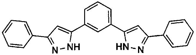
実施例1のリア側光学フィルムを作製するための主ドープは、以下の手順で調製した。まず、加圧溶解タンクに250質量部のメチレンクロライド(ジクロロメタン)と、50質量部のエタノールとを投入し、加熱しながら攪拌混合した。この加圧溶解タンクにセルロースアセテートプロピオネート(CAP)100質量部を、タンク内の混合液を攪拌しながら投入した。この加圧溶解タンク内の混合液を加熱し、攪拌してCAPを完全に溶解させた。このCAPの溶解液を安積濾紙(株)製の安積濾紙No.244を使用して濾過した。この濾過液に対し、質量比で4質量%のピラゾール化合物と、0.1質量%のシリカ系化合物(製品名:アエロジルR812(日本アエロジル株式会社製))とを配合して溶解釜に投入し、攪拌しながら溶解することによって主ドープを調製した。

まず、COPフィルムを構成する熱可塑性ノルボルネン系樹脂を作製した。窒素雰囲気下、脱水したシクロヘキサン500部に、1-ヘキセン0.82部、ジブチルエーテル0.15部およびトリイソブチルアルミニウム0.30部を室温で反応器に入れて混合した。次に、この混合溶液を45℃に保ちながら、トリシクロ〔4.3.0.12,5〕デカ-3,7-ジエン(以下、「DCP」とも記す)40部、7,8-ベンゾトリシクロ[4.3.0.12,5]デカ-3-エン(以下、「MTF」とも記す)100部およびテトラシクロ〔4.4.0,12,5.17,10〕ドデカ-3-エン(以下、「TCD」とも記す)60部からなるノルボルネン系モノマー混合物と、六塩化タングステン(0.7%トルエン溶液)40部とを2時間かけて連続的に添加して重合した。この重合溶液に対して、ブチルグリシジルエーテル1.06部と、イソプロピルアルコール0.52部とを加え、重合触媒を不活性化することにより重合反応を停止した。
(主ドープの調製)
フロント側光学フィルムを作製するために下記組成の主ドープを調製した。すなわち、まず、加圧溶解タンクにメチレンクロライドとエタノールを溶剤として投入した。そして、溶剤の入った加圧溶解タンクにセルロースアシレートと糖エステル、エステル化合物、マット材の分散液を、溶剤を攪拌しながら投入し、これらの混合液を加熱し、攪拌してセルロースアシレート等を完全に溶解させた。
糖エステルT1 12質量部
エステル化合物E1 4質量部
マット剤:R812の12%エタノール分散液(日本アエロジル株式会社製)
1.4質量部
メチレンクロライド 430質量部
エタノール 40質量部
セルロースアシレート:アセチル基置換度2.80である数平均分子量70000のセルローストリアセテート(TAC)
糖エステルT1:下記の化学式に示す糖エステル
上記で調製した主ドープを、ベルト流延装置を用い、温度22℃、1.8m幅でステンレスバンド支持体に均一に流延し、ドープ膜(ウェブ)とした。ステンレスバンド支持体で、ウェブ中の残留溶剤量が20%になるまで溶媒を蒸発させ、剥離張力162N/mでステンレスバンド支持体上からウェブを剥離し、樹脂フィルムを得た。
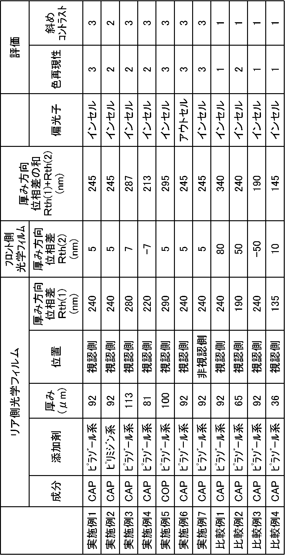
上記で作製したリア側光学フィルムおよびフロント側光学フィルムを組み合わせて上記表1の実施例1~7および比較例1~4の液晶表示装置を作製した。上記表1における「インセル」とは、リア側偏光板およびフロント側偏光板が一対のセル基板の内側に配置されているインセルタイプの液晶表示装置を意味する。上記表1における「アウトセル」とは、リア側偏光板およびフロント側偏光板が一対のセル基板の外側に配置されているアウトセルタイプの液晶表示装置を意味する。また、表1のリア側光学フィルムの「位置」の欄に示す「非視認側」とは、リア側光学フィルムがリア側偏光子の非視認側に配置されていることを意味する。表1における「視認側」とは、リア側光学フィルムがリア側偏光子の視認側に配置されていることを意味する。
実施例2~5および比較例1~4では、リア側光学フィルムおよびフロント側光学フィルムの厚み方向の位相差Rth(1)およびRth(2)を変更したことが異なる他は、実施例1と同様にして液晶表示装置を作製した。
実施例6では、図2に示すアウトセルタイプの液晶表示装置を作製した。具体的には、まず、ガラス基板の表面に透明電極が形成されたセル基板6を準備した。次に、このセル基板6の透明電極が形成された面の反対側の表面上にブラックマトリクスを形成した。次いで、ブラックマトリクスの対応する収容空間内に、赤色ドット微粒子を含む赤色フィルタ、緑色ドット微粒子を含む緑色フィルタ、および青色ドット微粒子を含む青色フィルタを、それぞれリソグラフィプロセスによって形成した。このようにして、セル基板6の面上に光変換層4を作製した。またセル基板6の光変換層4が形成された面とは反対側の面に粘着剤を介してフロント側偏光板5を貼り付けた。このフロント側偏光板5は、実施例1と同様の構成のものを用いた。
実施例7では、実施例1の液晶表示装置におけるリア側光学フィルムとリア側保護フィルムとを入れ替えたことが異なる他は実施例1と同様にして液晶表示装置を作製した。
各実施例および各比較例で作製した液晶表示装置の色再現性および斜めコントラストを以下に示す評価基準で評価した。
色再現性は、赤、緑、青の各色のそれぞれの画素のCIE 1931XYZ表色系における色度を(xR、yR)、(xG、yG)、(xB、yB)として特定し、x-y色度図上のこれらの三点で囲まれる三角形の面積の大小によって評価した。上記三角形の面積が大きいほど鮮やかなカラー画像が再現できることを意味する。この三角形の面積は、通常、全米テレビジョン放送方式標準化委員会(NTSC:National Television System Committee)により定められた標準方式の3原色、赤(0.67、0.33)、緑(0.21、0.71)、青(0.14,0.08)の三点で形成される三角形を基準として、この三角形の面積に対する比(単位%、以下「NTSC比」と略す。)によって表現される。
2:60%以上90%未満
1:60%未満
各実施例および各比較例の液晶表示装置の斜めコントラストについて、測定器(TOPCON社製:BM-5A)を用いて、暗室で装置正面からの極角方向60度、方位角方向0度、45度、90度における黒表示および白表示の輝度値を測定し、白輝度/黒輝度を算出し、各実施例および各比較例の液晶表示装置の視野角特性を以下の基準で評価した。この評価結果を表1の「斜めコントラスト」の欄に示す。
2:視野角コントラストの最小値が50未満25以上であり、わずかに光漏れが認識されるが許容できる程度。
1:視野角コントラスト最小値が25未満であり、大きな光漏れが認識され許容できない。
上記実施例1~7の液晶表示装置は、非白色光源と、リア側偏光子およびリア側光学フィルムを含むリア側偏光板と、液晶セルと、量子ドット微粒子を含有するカラーフィルタである光変換層と、フロント側光学フィルムおよびフロント側偏光子を含むフロント側偏光板とをこの順に含み、前記フロント側光学フィルムの厚み方向の位相差Rth(2)は、-10nm以上10nm以下であり、前記リア側光学フィルムの厚み方向の位相差Rth(1)と、前記Rth(2)との和は、200nm以上300nm以下であった。そのため、非白色光源から出射した光がリア側光学フィルムで位相変換された。これにより光変換層に到達した光による光変換層の発熱が抑えられ、量子ドット微粒子の分散状態に変動が生じなくなることで、色再現性に優れることが明らかとなり、本発明の効果が示された。
Claims (5)
- 非白色光源と、リア側偏光子およびリア側光学フィルムを含むリア側偏光板と、液晶セルと、量子ドット微粒子を含有するカラーフィルタである光変換層と、フロント側光学フィルムおよびフロント側偏光子を含むフロント側偏光板とをこの順に含み、
前記フロント側光学フィルムの厚み方向の位相差Rth(2)は、-10nm以上10nm以下であり、
前記リア側光学フィルムの厚み方向の位相差Rth(1)と、前記Rth(2)との和は、200nm以上300nm以下である液晶表示装置。 - 前記リア側光学フィルムは、ピラゾール系化合物を含む請求項1に記載の液晶表示装置。
- 前記液晶セルは、VAモードまたはIPSモードである請求項1または2に記載の液晶表示装置。
- 前記リア側光学フィルムの厚み方向の位相差Rth(1)は、200nm以上280nm以下である請求項1~3のいずれか一項に記載の液晶表示装置。
- 非白色光源と、リア側偏光子およびリア側光学フィルムを含むリア側偏光板と、液晶セルと、量子ドット微粒子を含有するカラーフィルタである光変換層と、フロント側光学フィルムおよびフロント側偏光子を含むフロント側偏光板とをこの順に含む液晶表示装置に用いられる一対の光学フィルムであって、
前記一対の光学フィルムの一方は、前記フロント側光学フィルムとして用いられ、その厚み方向の位相差Rth(2)は、-10nm以上10nm以下であり、
前記一対の光学フィルムの他方は、前記リア側光学フィルムとして用いられ、その厚み方向の位相差Rth(1)と、前記Rth(2)との和は、200nm以上300nm以下である一対の光学フィルム。
Priority Applications (1)
| Application Number | Priority Date | Filing Date | Title |
|---|---|---|---|
| KR1020197025261A KR102214975B1 (ko) | 2017-03-02 | 2018-01-18 | 액정 표시 장치 및 이 액정 표시 장치에 사용되는 한 쌍의 광학 필름 |
Applications Claiming Priority (2)
| Application Number | Priority Date | Filing Date | Title |
|---|---|---|---|
| JP2017039608 | 2017-03-02 | ||
| JP2017-039608 | 2017-03-02 |
Publications (1)
| Publication Number | Publication Date |
|---|---|
| WO2018159130A1 true WO2018159130A1 (ja) | 2018-09-07 |
Family
ID=63371384
Family Applications (1)
| Application Number | Title | Priority Date | Filing Date |
|---|---|---|---|
| PCT/JP2018/001300 Ceased WO2018159130A1 (ja) | 2017-03-02 | 2018-01-18 | 液晶表示装置およびこの液晶表示装置に用いられる一対の光学フィルム |
Country Status (2)
| Country | Link |
|---|---|
| KR (1) | KR102214975B1 (ja) |
| WO (1) | WO2018159130A1 (ja) |
Cited By (1)
| Publication number | Priority date | Publication date | Assignee | Title |
|---|---|---|---|---|
| CN109407391A (zh) * | 2018-12-25 | 2019-03-01 | 深圳市华星光电半导体显示技术有限公司 | 透明液晶显示装置 |
Citations (2)
| Publication number | Priority date | Publication date | Assignee | Title |
|---|---|---|---|---|
| WO2010089930A1 (ja) * | 2009-02-09 | 2010-08-12 | シャープ株式会社 | 液晶表示パネル |
| JP2016212348A (ja) * | 2015-05-13 | 2016-12-15 | 株式会社 オルタステクノロジー | 液晶表示装置 |
Family Cites Families (3)
| Publication number | Priority date | Publication date | Assignee | Title |
|---|---|---|---|---|
| JP2013235150A (ja) | 2012-05-09 | 2013-11-21 | Konica Minolta Inc | 液晶表示装置 |
| JP6144995B2 (ja) | 2013-08-13 | 2017-06-07 | 富士フイルム株式会社 | 液晶表示装置 |
| KR101995930B1 (ko) | 2015-02-25 | 2019-07-03 | 동우 화인켐 주식회사 | 양자점을 포함하는 경화 조성물, 이를 이용하여 제조된 컬러필터 및 화상표시장치 |
-
2018
- 2018-01-18 WO PCT/JP2018/001300 patent/WO2018159130A1/ja not_active Ceased
- 2018-01-18 KR KR1020197025261A patent/KR102214975B1/ko active Active
Patent Citations (2)
| Publication number | Priority date | Publication date | Assignee | Title |
|---|---|---|---|---|
| WO2010089930A1 (ja) * | 2009-02-09 | 2010-08-12 | シャープ株式会社 | 液晶表示パネル |
| JP2016212348A (ja) * | 2015-05-13 | 2016-12-15 | 株式会社 オルタステクノロジー | 液晶表示装置 |
Cited By (2)
| Publication number | Priority date | Publication date | Assignee | Title |
|---|---|---|---|---|
| CN109407391A (zh) * | 2018-12-25 | 2019-03-01 | 深圳市华星光电半导体显示技术有限公司 | 透明液晶显示装置 |
| CN109407391B (zh) * | 2018-12-25 | 2020-12-08 | 深圳市华星光电半导体显示技术有限公司 | 透明液晶显示装置 |
Also Published As
| Publication number | Publication date |
|---|---|
| KR102214975B1 (ko) | 2021-02-09 |
| KR20190108615A (ko) | 2019-09-24 |
Similar Documents
| Publication | Publication Date | Title |
|---|---|---|
| JP5401032B2 (ja) | 光学異方性膜、輝度向上フィルム、位相差板および液晶表示装置 | |
| KR20080058248A (ko) | 액정 표시 장치 | |
| JP2014145852A (ja) | 光学フィルム、円偏光板および画像表示装置 | |
| JP5083483B1 (ja) | 長尺延伸フィルムの製造方法 | |
| CN115315644A (zh) | 光学各向异性层、光学膜、偏振片及图像显示装置 | |
| JP5565281B2 (ja) | 斜め延伸フィルムの製造方法、及び光学フィルムの製造方法 | |
| WO2014192681A1 (ja) | 樹脂組成物、光学部材、光学フィルム、偏光板、円偏光板及び画像表示装置 | |
| US12196995B2 (en) | Laminate, circularly polarizing plate, and display device | |
| WO2019151312A1 (ja) | 積層体 | |
| KR101654451B1 (ko) | 위상차 필름의 제조 방법, 편광판 및 액정 표시 장치 | |
| US8089593B2 (en) | Optical resin film, optical compensation sheet, polarizing plate and liquid crystal display | |
| JP6927285B2 (ja) | 光学フィルム、その製造方法、それを具備した偏光板及び表示装置 | |
| KR102214975B1 (ko) | 액정 표시 장치 및 이 액정 표시 장치에 사용되는 한 쌍의 광학 필름 | |
| JP2007017958A (ja) | 液晶表示装置 | |
| JP2006293342A (ja) | 光学樹脂フィルム、偏光板及び液晶表示装置 | |
| JP5979224B2 (ja) | 長尺延伸フィルムの製造方法及び製造装置 | |
| JP5083482B1 (ja) | 長尺延伸フィルムの製造方法 | |
| JP4383435B2 (ja) | 液晶表示装置 | |
| JP5862686B2 (ja) | 長尺延伸フィルムの製造方法 | |
| JP4953876B2 (ja) | 光学フィルムの製造方法、光学フィルム、偏光板、及び液晶表示装置 | |
| JP7405013B2 (ja) | 長尺の円偏光板、長尺の広帯域λ/4板、有機エレクトロルミネッセンス表示装置、及び、液晶表示装置 | |
| JP4939267B2 (ja) | 光学補償フィルム、及びその製造方法、並びにそれを用いた偏光板、及び液晶表示装置 | |
| KR102225417B1 (ko) | 액정 표시 장치 및 이 액정 표시 장치에 사용되는 한 쌍의 광학 필름 | |
| JP2017194620A (ja) | 偏光板および液晶表示装置 | |
| JP2007131704A (ja) | 環状オレフィン系重合体、およびそれを用いた光学材料、偏光板および液晶表示装置 |
Legal Events
| Date | Code | Title | Description |
|---|---|---|---|
| 121 | Ep: the epo has been informed by wipo that ep was designated in this application |
Ref document number: 18761076 Country of ref document: EP Kind code of ref document: A1 |
|
| ENP | Entry into the national phase |
Ref document number: 20197025261 Country of ref document: KR Kind code of ref document: A |
|
| NENP | Non-entry into the national phase |
Ref country code: DE |
|
| 122 | Ep: pct application non-entry in european phase |
Ref document number: 18761076 Country of ref document: EP Kind code of ref document: A1 |
|
| NENP | Non-entry into the national phase |
Ref country code: JP |