WO2018155478A1 - 基板処理装置、および、処理システム - Google Patents
基板処理装置、および、処理システム Download PDFInfo
- Publication number
- WO2018155478A1 WO2018155478A1 PCT/JP2018/006163 JP2018006163W WO2018155478A1 WO 2018155478 A1 WO2018155478 A1 WO 2018155478A1 JP 2018006163 W JP2018006163 W JP 2018006163W WO 2018155478 A1 WO2018155478 A1 WO 2018155478A1
- Authority
- WO
- WIPO (PCT)
- Prior art keywords
- substrate
- end surface
- unit
- cooling
- heating
- Prior art date
- Legal status (The legal status is an assumption and is not a legal conclusion. Google has not performed a legal analysis and makes no representation as to the accuracy of the status listed.)
- Ceased
Links
Images




Classifications
-
- C—CHEMISTRY; METALLURGY
- C23—COATING METALLIC MATERIAL; COATING MATERIAL WITH METALLIC MATERIAL; CHEMICAL SURFACE TREATMENT; DIFFUSION TREATMENT OF METALLIC MATERIAL; COATING BY VACUUM EVAPORATION, BY SPUTTERING, BY ION IMPLANTATION OR BY CHEMICAL VAPOUR DEPOSITION, IN GENERAL; INHIBITING CORROSION OF METALLIC MATERIAL OR INCRUSTATION IN GENERAL
- C23C—COATING METALLIC MATERIAL; COATING MATERIAL WITH METALLIC MATERIAL; SURFACE TREATMENT OF METALLIC MATERIAL BY DIFFUSION INTO THE SURFACE, BY CHEMICAL CONVERSION OR SUBSTITUTION; COATING BY VACUUM EVAPORATION, BY SPUTTERING, BY ION IMPLANTATION OR BY CHEMICAL VAPOUR DEPOSITION, IN GENERAL
- C23C14/00—Coating by vacuum evaporation, by sputtering or by ion implantation of the coating forming material
- C23C14/22—Coating by vacuum evaporation, by sputtering or by ion implantation of the coating forming material characterised by the process of coating
- C23C14/54—Controlling or regulating the coating process
- C23C14/541—Heating or cooling of the substrates
-
- H—ELECTRICITY
- H10—SEMICONDUCTOR DEVICES; ELECTRIC SOLID-STATE DEVICES NOT OTHERWISE PROVIDED FOR
- H10N—ELECTRIC SOLID-STATE DEVICES NOT OTHERWISE PROVIDED FOR
- H10N50/00—Galvanomagnetic devices
- H10N50/01—Manufacture or treatment
-
- H—ELECTRICITY
- H10—SEMICONDUCTOR DEVICES; ELECTRIC SOLID-STATE DEVICES NOT OTHERWISE PROVIDED FOR
- H10P—GENERIC PROCESSES OR APPARATUS FOR THE MANUFACTURE OR TREATMENT OF DEVICES COVERED BY CLASS H10
- H10P72/00—Handling or holding of wafers, substrates or devices during manufacture or treatment thereof
- H10P72/04—Apparatus for manufacture or treatment
- H10P72/0451—Apparatus for manufacturing or treating in a plurality of work-stations
- H10P72/0462—Apparatus for manufacturing or treating in a plurality of work-stations characterised by the construction of the processing chambers, e.g. modular processing chambers
-
- C—CHEMISTRY; METALLURGY
- C21—METALLURGY OF IRON
- C21D—MODIFYING THE PHYSICAL STRUCTURE OF FERROUS METALS; GENERAL DEVICES FOR HEAT TREATMENT OF FERROUS OR NON-FERROUS METALS OR ALLOYS; MAKING METAL MALLEABLE, e.g. BY DECARBURISATION OR TEMPERING
- C21D1/00—General methods or devices for heat treatment, e.g. annealing, hardening, quenching or tempering
- C21D1/04—General methods or devices for heat treatment, e.g. annealing, hardening, quenching or tempering with simultaneous application of supersonic waves, magnetic or electric fields
-
- C—CHEMISTRY; METALLURGY
- C23—COATING METALLIC MATERIAL; COATING MATERIAL WITH METALLIC MATERIAL; CHEMICAL SURFACE TREATMENT; DIFFUSION TREATMENT OF METALLIC MATERIAL; COATING BY VACUUM EVAPORATION, BY SPUTTERING, BY ION IMPLANTATION OR BY CHEMICAL VAPOUR DEPOSITION, IN GENERAL; INHIBITING CORROSION OF METALLIC MATERIAL OR INCRUSTATION IN GENERAL
- C23C—COATING METALLIC MATERIAL; COATING MATERIAL WITH METALLIC MATERIAL; SURFACE TREATMENT OF METALLIC MATERIAL BY DIFFUSION INTO THE SURFACE, BY CHEMICAL CONVERSION OR SUBSTITUTION; COATING BY VACUUM EVAPORATION, BY SPUTTERING, BY ION IMPLANTATION OR BY CHEMICAL VAPOUR DEPOSITION, IN GENERAL
- C23C14/00—Coating by vacuum evaporation, by sputtering or by ion implantation of the coating forming material
- C23C14/22—Coating by vacuum evaporation, by sputtering or by ion implantation of the coating forming material characterised by the process of coating
- C23C14/50—Substrate holders
-
- C—CHEMISTRY; METALLURGY
- C23—COATING METALLIC MATERIAL; COATING MATERIAL WITH METALLIC MATERIAL; CHEMICAL SURFACE TREATMENT; DIFFUSION TREATMENT OF METALLIC MATERIAL; COATING BY VACUUM EVAPORATION, BY SPUTTERING, BY ION IMPLANTATION OR BY CHEMICAL VAPOUR DEPOSITION, IN GENERAL; INHIBITING CORROSION OF METALLIC MATERIAL OR INCRUSTATION IN GENERAL
- C23C—COATING METALLIC MATERIAL; COATING MATERIAL WITH METALLIC MATERIAL; SURFACE TREATMENT OF METALLIC MATERIAL BY DIFFUSION INTO THE SURFACE, BY CHEMICAL CONVERSION OR SUBSTITUTION; COATING BY VACUUM EVAPORATION, BY SPUTTERING, BY ION IMPLANTATION OR BY CHEMICAL VAPOUR DEPOSITION, IN GENERAL
- C23C14/00—Coating by vacuum evaporation, by sputtering or by ion implantation of the coating forming material
- C23C14/22—Coating by vacuum evaporation, by sputtering or by ion implantation of the coating forming material characterised by the process of coating
- C23C14/52—Means for observation of the coating process
-
- C—CHEMISTRY; METALLURGY
- C23—COATING METALLIC MATERIAL; COATING MATERIAL WITH METALLIC MATERIAL; CHEMICAL SURFACE TREATMENT; DIFFUSION TREATMENT OF METALLIC MATERIAL; COATING BY VACUUM EVAPORATION, BY SPUTTERING, BY ION IMPLANTATION OR BY CHEMICAL VAPOUR DEPOSITION, IN GENERAL; INHIBITING CORROSION OF METALLIC MATERIAL OR INCRUSTATION IN GENERAL
- C23C—COATING METALLIC MATERIAL; COATING MATERIAL WITH METALLIC MATERIAL; SURFACE TREATMENT OF METALLIC MATERIAL BY DIFFUSION INTO THE SURFACE, BY CHEMICAL CONVERSION OR SUBSTITUTION; COATING BY VACUUM EVAPORATION, BY SPUTTERING, BY ION IMPLANTATION OR BY CHEMICAL VAPOUR DEPOSITION, IN GENERAL
- C23C14/00—Coating by vacuum evaporation, by sputtering or by ion implantation of the coating forming material
- C23C14/22—Coating by vacuum evaporation, by sputtering or by ion implantation of the coating forming material characterised by the process of coating
- C23C14/56—Apparatus specially adapted for continuous coating; Arrangements for maintaining the vacuum, e.g. vacuum locks
- C23C14/564—Means for minimising impurities in the coating chamber such as dust, moisture, residual gases
- C23C14/566—Means for minimising impurities in the coating chamber such as dust, moisture, residual gases using a load-lock chamber
-
- C—CHEMISTRY; METALLURGY
- C23—COATING METALLIC MATERIAL; COATING MATERIAL WITH METALLIC MATERIAL; CHEMICAL SURFACE TREATMENT; DIFFUSION TREATMENT OF METALLIC MATERIAL; COATING BY VACUUM EVAPORATION, BY SPUTTERING, BY ION IMPLANTATION OR BY CHEMICAL VAPOUR DEPOSITION, IN GENERAL; INHIBITING CORROSION OF METALLIC MATERIAL OR INCRUSTATION IN GENERAL
- C23C—COATING METALLIC MATERIAL; COATING MATERIAL WITH METALLIC MATERIAL; SURFACE TREATMENT OF METALLIC MATERIAL BY DIFFUSION INTO THE SURFACE, BY CHEMICAL CONVERSION OR SUBSTITUTION; COATING BY VACUUM EVAPORATION, BY SPUTTERING, BY ION IMPLANTATION OR BY CHEMICAL VAPOUR DEPOSITION, IN GENERAL
- C23C14/00—Coating by vacuum evaporation, by sputtering or by ion implantation of the coating forming material
- C23C14/58—After-treatment
-
- C—CHEMISTRY; METALLURGY
- C23—COATING METALLIC MATERIAL; COATING MATERIAL WITH METALLIC MATERIAL; CHEMICAL SURFACE TREATMENT; DIFFUSION TREATMENT OF METALLIC MATERIAL; COATING BY VACUUM EVAPORATION, BY SPUTTERING, BY ION IMPLANTATION OR BY CHEMICAL VAPOUR DEPOSITION, IN GENERAL; INHIBITING CORROSION OF METALLIC MATERIAL OR INCRUSTATION IN GENERAL
- C23C—COATING METALLIC MATERIAL; COATING MATERIAL WITH METALLIC MATERIAL; SURFACE TREATMENT OF METALLIC MATERIAL BY DIFFUSION INTO THE SURFACE, BY CHEMICAL CONVERSION OR SUBSTITUTION; COATING BY VACUUM EVAPORATION, BY SPUTTERING, BY ION IMPLANTATION OR BY CHEMICAL VAPOUR DEPOSITION, IN GENERAL
- C23C14/00—Coating by vacuum evaporation, by sputtering or by ion implantation of the coating forming material
- C23C14/58—After-treatment
- C23C14/5806—Thermal treatment
-
- C—CHEMISTRY; METALLURGY
- C23—COATING METALLIC MATERIAL; COATING MATERIAL WITH METALLIC MATERIAL; CHEMICAL SURFACE TREATMENT; DIFFUSION TREATMENT OF METALLIC MATERIAL; COATING BY VACUUM EVAPORATION, BY SPUTTERING, BY ION IMPLANTATION OR BY CHEMICAL VAPOUR DEPOSITION, IN GENERAL; INHIBITING CORROSION OF METALLIC MATERIAL OR INCRUSTATION IN GENERAL
- C23C—COATING METALLIC MATERIAL; COATING MATERIAL WITH METALLIC MATERIAL; SURFACE TREATMENT OF METALLIC MATERIAL BY DIFFUSION INTO THE SURFACE, BY CHEMICAL CONVERSION OR SUBSTITUTION; COATING BY VACUUM EVAPORATION, BY SPUTTERING, BY ION IMPLANTATION OR BY CHEMICAL VAPOUR DEPOSITION, IN GENERAL
- C23C14/00—Coating by vacuum evaporation, by sputtering or by ion implantation of the coating forming material
- C23C14/58—After-treatment
- C23C14/584—Non-reactive treatment
-
- F—MECHANICAL ENGINEERING; LIGHTING; HEATING; WEAPONS; BLASTING
- F27—FURNACES; KILNS; OVENS; RETORTS
- F27B—FURNACES, KILNS, OVENS OR RETORTS IN GENERAL; OPEN SINTERING OR LIKE APPARATUS
- F27B14/00—Crucible or pot furnaces
- F27B14/08—Details specially adapted for crucible or pot furnaces
- F27B14/14—Arrangements of heating devices
-
- F—MECHANICAL ENGINEERING; LIGHTING; HEATING; WEAPONS; BLASTING
- F27—FURNACES; KILNS; OVENS; RETORTS
- F27D—DETAILS OR ACCESSORIES OF FURNACES, KILNS, OVENS OR RETORTS, IN SO FAR AS THEY ARE OF KINDS OCCURRING IN MORE THAN ONE KIND OF FURNACE
- F27D11/00—Arrangement of elements for electric heating in or on furnaces
- F27D11/12—Arrangement of elements for electric heating in or on furnaces with electromagnetic fields acting directly on the material being heated
-
- G—PHYSICS
- G11—INFORMATION STORAGE
- G11B—INFORMATION STORAGE BASED ON RELATIVE MOVEMENT BETWEEN RECORD CARRIER AND TRANSDUCER
- G11B5/00—Recording by magnetisation or demagnetisation of a record carrier; Reproducing by magnetic means; Record carriers therefor
- G11B5/127—Structure or manufacture of heads, e.g. inductive
- G11B5/31—Structure or manufacture of heads, e.g. inductive using thin films
- G11B5/3163—Fabrication methods or processes specially adapted for a particular head structure, e.g. using base layers for electroplating, using functional layers for masking, using energy or particle beams for shaping the structure or modifying the properties of the basic layers
-
- H—ELECTRICITY
- H01—ELECTRIC ELEMENTS
- H01F—MAGNETS; INDUCTANCES; TRANSFORMERS; SELECTION OF MATERIALS FOR THEIR MAGNETIC PROPERTIES
- H01F41/00—Apparatus or processes specially adapted for manufacturing or assembling magnets, inductances or transformers; Apparatus or processes specially adapted for manufacturing materials characterised by their magnetic properties
- H01F41/14—Apparatus or processes specially adapted for manufacturing or assembling magnets, inductances or transformers; Apparatus or processes specially adapted for manufacturing materials characterised by their magnetic properties for applying magnetic films to substrates
- H01F41/22—Heat treatment; Thermal decomposition; Chemical vapour deposition
-
- H—ELECTRICITY
- H10—SEMICONDUCTOR DEVICES; ELECTRIC SOLID-STATE DEVICES NOT OTHERWISE PROVIDED FOR
- H10B—ELECTRONIC MEMORY DEVICES
- H10B61/00—Magnetic memory devices, e.g. magnetoresistive RAM [MRAM] devices
-
- H—ELECTRICITY
- H10—SEMICONDUCTOR DEVICES; ELECTRIC SOLID-STATE DEVICES NOT OTHERWISE PROVIDED FOR
- H10N—ELECTRIC SOLID-STATE DEVICES NOT OTHERWISE PROVIDED FOR
- H10N50/00—Galvanomagnetic devices
- H10N50/10—Magnetoresistive devices
-
- H—ELECTRICITY
- H10—SEMICONDUCTOR DEVICES; ELECTRIC SOLID-STATE DEVICES NOT OTHERWISE PROVIDED FOR
- H10P—GENERIC PROCESSES OR APPARATUS FOR THE MANUFACTURE OR TREATMENT OF DEVICES COVERED BY CLASS H10
- H10P34/00—Irradiation with electromagnetic or particle radiation of wafers, substrates or parts of devices
-
- H—ELECTRICITY
- H10—SEMICONDUCTOR DEVICES; ELECTRIC SOLID-STATE DEVICES NOT OTHERWISE PROVIDED FOR
- H10P—GENERIC PROCESSES OR APPARATUS FOR THE MANUFACTURE OR TREATMENT OF DEVICES COVERED BY CLASS H10
- H10P72/00—Handling or holding of wafers, substrates or devices during manufacture or treatment thereof
- H10P72/04—Apparatus for manufacture or treatment
- H10P72/0402—Apparatus for fluid treatment
-
- H—ELECTRICITY
- H10—SEMICONDUCTOR DEVICES; ELECTRIC SOLID-STATE DEVICES NOT OTHERWISE PROVIDED FOR
- H10P—GENERIC PROCESSES OR APPARATUS FOR THE MANUFACTURE OR TREATMENT OF DEVICES COVERED BY CLASS H10
- H10P72/00—Handling or holding of wafers, substrates or devices during manufacture or treatment thereof
- H10P72/04—Apparatus for manufacture or treatment
- H10P72/0431—Apparatus for thermal treatment
-
- H—ELECTRICITY
- H10—SEMICONDUCTOR DEVICES; ELECTRIC SOLID-STATE DEVICES NOT OTHERWISE PROVIDED FOR
- H10P—GENERIC PROCESSES OR APPARATUS FOR THE MANUFACTURE OR TREATMENT OF DEVICES COVERED BY CLASS H10
- H10P72/00—Handling or holding of wafers, substrates or devices during manufacture or treatment thereof
- H10P72/04—Apparatus for manufacture or treatment
- H10P72/0431—Apparatus for thermal treatment
- H10P72/0432—Apparatus for thermal treatment mainly by conduction
-
- H—ELECTRICITY
- H10—SEMICONDUCTOR DEVICES; ELECTRIC SOLID-STATE DEVICES NOT OTHERWISE PROVIDED FOR
- H10P—GENERIC PROCESSES OR APPARATUS FOR THE MANUFACTURE OR TREATMENT OF DEVICES COVERED BY CLASS H10
- H10P72/00—Handling or holding of wafers, substrates or devices during manufacture or treatment thereof
- H10P72/04—Apparatus for manufacture or treatment
- H10P72/0431—Apparatus for thermal treatment
- H10P72/0434—Apparatus for thermal treatment mainly by convection
-
- H—ELECTRICITY
- H10—SEMICONDUCTOR DEVICES; ELECTRIC SOLID-STATE DEVICES NOT OTHERWISE PROVIDED FOR
- H10P—GENERIC PROCESSES OR APPARATUS FOR THE MANUFACTURE OR TREATMENT OF DEVICES COVERED BY CLASS H10
- H10P72/00—Handling or holding of wafers, substrates or devices during manufacture or treatment thereof
- H10P72/04—Apparatus for manufacture or treatment
- H10P72/0451—Apparatus for manufacturing or treating in a plurality of work-stations
- H10P72/0452—Apparatus for manufacturing or treating in a plurality of work-stations characterised by the layout of the process chambers
- H10P72/0454—Apparatus for manufacturing or treating in a plurality of work-stations characterised by the layout of the process chambers surrounding a central transfer chamber
-
- H—ELECTRICITY
- H10—SEMICONDUCTOR DEVICES; ELECTRIC SOLID-STATE DEVICES NOT OTHERWISE PROVIDED FOR
- H10P—GENERIC PROCESSES OR APPARATUS FOR THE MANUFACTURE OR TREATMENT OF DEVICES COVERED BY CLASS H10
- H10P72/00—Handling or holding of wafers, substrates or devices during manufacture or treatment thereof
- H10P72/04—Apparatus for manufacture or treatment
- H10P72/0451—Apparatus for manufacturing or treating in a plurality of work-stations
- H10P72/0464—Apparatus for manufacturing or treating in a plurality of work-stations characterised by the construction of the transfer chamber
-
- H—ELECTRICITY
- H10—SEMICONDUCTOR DEVICES; ELECTRIC SOLID-STATE DEVICES NOT OTHERWISE PROVIDED FOR
- H10P—GENERIC PROCESSES OR APPARATUS FOR THE MANUFACTURE OR TREATMENT OF DEVICES COVERED BY CLASS H10
- H10P72/00—Handling or holding of wafers, substrates or devices during manufacture or treatment thereof
- H10P72/06—Apparatus for monitoring, sorting, marking, testing or measuring
- H10P72/0604—Process monitoring, e.g. flow or thickness monitoring
-
- H—ELECTRICITY
- H10—SEMICONDUCTOR DEVICES; ELECTRIC SOLID-STATE DEVICES NOT OTHERWISE PROVIDED FOR
- H10P—GENERIC PROCESSES OR APPARATUS FOR THE MANUFACTURE OR TREATMENT OF DEVICES COVERED BY CLASS H10
- H10P72/00—Handling or holding of wafers, substrates or devices during manufacture or treatment thereof
- H10P72/06—Apparatus for monitoring, sorting, marking, testing or measuring
- H10P72/0606—Position monitoring, e.g. misposition detection or presence detection
-
- H—ELECTRICITY
- H10—SEMICONDUCTOR DEVICES; ELECTRIC SOLID-STATE DEVICES NOT OTHERWISE PROVIDED FOR
- H10P—GENERIC PROCESSES OR APPARATUS FOR THE MANUFACTURE OR TREATMENT OF DEVICES COVERED BY CLASS H10
- H10P72/00—Handling or holding of wafers, substrates or devices during manufacture or treatment thereof
- H10P72/30—Handling or holding of wafers, substrates or devices during manufacture or treatment thereof for conveying, e.g. between different workstations
-
- H—ELECTRICITY
- H10—SEMICONDUCTOR DEVICES; ELECTRIC SOLID-STATE DEVICES NOT OTHERWISE PROVIDED FOR
- H10P—GENERIC PROCESSES OR APPARATUS FOR THE MANUFACTURE OR TREATMENT OF DEVICES COVERED BY CLASS H10
- H10P72/00—Handling or holding of wafers, substrates or devices during manufacture or treatment thereof
- H10P72/30—Handling or holding of wafers, substrates or devices during manufacture or treatment thereof for conveying, e.g. between different workstations
- H10P72/33—Handling or holding of wafers, substrates or devices during manufacture or treatment thereof for conveying, e.g. between different workstations into and out of processing chamber
- H10P72/3302—Mechanical parts of transfer devices
-
- H—ELECTRICITY
- H10—SEMICONDUCTOR DEVICES; ELECTRIC SOLID-STATE DEVICES NOT OTHERWISE PROVIDED FOR
- H10P—GENERIC PROCESSES OR APPARATUS FOR THE MANUFACTURE OR TREATMENT OF DEVICES COVERED BY CLASS H10
- H10P72/00—Handling or holding of wafers, substrates or devices during manufacture or treatment thereof
- H10P72/70—Handling or holding of wafers, substrates or devices during manufacture or treatment thereof for supporting or gripping
-
- H—ELECTRICITY
- H10—SEMICONDUCTOR DEVICES; ELECTRIC SOLID-STATE DEVICES NOT OTHERWISE PROVIDED FOR
- H10P—GENERIC PROCESSES OR APPARATUS FOR THE MANUFACTURE OR TREATMENT OF DEVICES COVERED BY CLASS H10
- H10P95/00—Generic processes or apparatus for manufacture or treatments not covered by the other groups of this subclass
- H10P95/90—Thermal treatments, e.g. annealing or sintering
Definitions
- Embodiments described herein relate generally to a substrate processing apparatus and a processing system.
- Patent Document 1 discloses a technique related to a vacuum heating / cooling apparatus for the purpose of rapidly heating and rapidly cooling only a substrate while maintaining a high degree of vacuum after film formation.
- Patent Document 2 discloses a technique related to a magnetic annealing apparatus intended to reduce the adhesion of impurities to a semiconductor wafer.
- a plurality of MTJ elements sequentially taken out from the single-wafer PVD film forming apparatus after film formation are collectively transported to an apparatus different from the PVD film forming apparatus and magnetized in the apparatus.
- a characteristic evaluation such as a magnetoresistance ratio
- CIPT Current-In-Plane Tunneling
- the plurality of MTJ elements can be treated as manufactured in a manufacturing process in which a failure may occur. Therefore, it is desired to provide a substrate processing apparatus and a processing system that can perform magnetization processing and annealing processing on a single wafer after film formation in an MRAM manufacturing process.
- a substrate processing apparatus is provided.
- the substrate processing apparatus is a substrate processing apparatus that processes a substrate having a magnetic layer into a single wafer, a support unit that supports the substrate, a heating unit that heats the substrate supported by the support unit, and a support unit that supports the substrate.
- a cooling unit that cools the substrate to be processed, a support unit, a heating unit, a processing container that houses the cooling unit, and a magnet unit that generates a magnetic field, the magnet units extending in parallel with each other
- the first end surface and the second end surface are spaced apart from each other, the first end surface corresponds to the first magnetic pole of the magnet portion, and the second end surface is provided with an end surface and a second end surface.
- the processing container is disposed between the first end face and the second end face.
- the magnet unit, the substrate support unit, the heating unit, and the cooling unit necessary for the magnetization process and annealing process for the substrate having the magnetic layer are provided in one substrate processing apparatus that processes the substrate into a single wafer. Therefore, the magnetization process and the annealing process for the substrate can be performed for each substrate. Therefore, in the above aspect, for example, in the MRAM manufacturing process, the magnetization process and the annealing process can be performed on a single wafer after film formation.
- the substrate in a state where the substrate is supported by the support portion, the substrate is included in the first end surface and the second end surface as viewed from the first end surface and the second end surface. It extends in parallel to the end face and the second end face. Accordingly, the lines of magnetic force generated between the first end surface and the second end surface in the magnet portion can be perpendicular to the direction in which the substrate supported by the support portion extends (perpendicular to the substrate). .
- the cooling unit is disposed in the processing container between a position where the substrate is disposed in the processing container (referred to as an arrangement position) and the first end surface when the substrate is supported by the support unit.
- the heating unit is disposed between the arrangement position and the cooling unit.
- a moving mechanism for moving the substrate is further provided.
- the moving mechanism moves the substrate so as to approach and separate from the cooling unit while being parallel to the first end surface and the second end surface in a state where the substrate is supported by the support unit. Therefore, when cooling the substrate, the substrate can be brought closer to the cooling unit, so that the substrate can be cooled more effectively.
- the cooling unit is disposed in the processing container between a position where the substrate is disposed in the processing container (referred to as an arrangement position) and the first end surface when the substrate is supported by the support unit.
- the heating unit is disposed between the arrangement position and the cooling unit.
- the heating unit includes a first heating layer and a second heating layer.
- the cooling unit includes a first cooling layer and a second cooling layer.
- the first cooling layer is disposed in the processing container between a position where the substrate is disposed in the processing container when the substrate is supported by the support portion (referred to as an disposed position) and the first end surface.
- the second cooling layer is arranged between the arrangement position and the second end surface in the processing container.
- the first heating layer is arranged between the arrangement position and the first cooling layer, and the second heating layer is arranged between the arrangement position and the second cooling layer.
- a processing system includes a plurality of film forming apparatuses, a substrate processing apparatus according to any of the above aspects and embodiments, and a measurement apparatus.
- the film formation apparatus forms a substrate having a magnetic layer
- the substrate processing apparatus processes the substrate formed by the film formation apparatus into a single wafer
- the measurement apparatus includes a substrate formed by the film formation apparatus, and a substrate An electromagnetic characteristic value is measured on a single wafer for the substrate after being processed by the processing apparatus.
- the magnet unit, the substrate support unit, the heating unit, and the cooling unit necessary for the magnetization process and annealing process for the substrate having the magnetic layer are provided in one substrate processing apparatus that processes the substrate into a single wafer.
- the magnetizing process and the annealing process for the substrate can be performed for each substrate, and the substrate formed by the film forming apparatus and the electromagnetic for the substrate after the magnetizing process and the annealing process are performed.
- the measurement of the characteristic value can be performed on the single wafer.
- the apparatus further includes an atmospheric transfer chamber, and the measurement device is connected to the atmospheric transfer chamber.
- the measurement apparatus since the measurement apparatus can be installed via the atmospheric transfer chamber of the processing system, restrictions on the installation location of the measurement apparatus are reduced, and thus the measurement apparatus can be easily installed.
- the electromagnetic property value is a magnetoresistance ratio.
- the electromagnetic characteristics of the substrate can be evaluated well.
- a substrate processing apparatus and a processing system capable of performing a magnetization process and an annealing process on a single wafer after film formation in an MRAM manufacturing process.
- FIG. 1 is a diagram illustrating an example of a main configuration of a substrate processing apparatus according to an embodiment.
- FIG. 2 is a diagram illustrating an example of a main configuration of a processing system including the substrate processing apparatus illustrated in FIG.
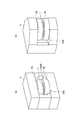
- FIG. 3 is a perspective view illustrating the appearance of the substrate processing apparatus shown in FIG. 1, which includes the (a) part and the (b) part. In particular, each of two types of shapes of the yoke of the substrate processing apparatus is shown in FIG. (A) part and FIG. 3 (b) part.
- FIG. 4 is a diagram schematically illustrating one mode of a heating unit and a cooling unit provided in the processing container illustrated in FIG. 1.
- FIG. 1 is a diagram illustrating an example of a main configuration of a substrate processing apparatus according to an embodiment.
- FIG. 2 is a diagram illustrating an example of a main configuration of a processing system including the substrate processing apparatus illustrated in FIG.
- FIG. 3 is a perspective view illustrating the appearance of the substrate processing apparatus shown in FIG.
- FIG. 5 is a diagram schematically illustrating another aspect of the heating unit and the cooling unit provided in the processing container illustrated in FIG. 1.
- FIG. 6 is a diagram schematically illustrating another aspect of the heating unit and the cooling unit provided in the processing container illustrated in FIG. 1.
- FIG. 7 is a flowchart showing the contents of processing performed by the processing system shown in FIG.
- FIG. 1 is a diagram illustrating an example of a main configuration of a substrate processing apparatus 10 according to an embodiment.
- the substrate processing apparatus 10 is used for manufacturing an MRAM, and after forming an MTJ element (for example, an element having an MgO / CoFeB laminated film) formed on a substrate having a magnetic layer (hereinafter also referred to as a wafer W), It is an apparatus that performs a magnetizing process and an annealing process.
- the substrate processing apparatus 10 can be used by being provided in a processing system 100 shown in FIG.
- the substrate processing apparatus 10 includes a substrate processing apparatus 10, a magnet unit 2, a power source EF, a wire unit 3a, a wire unit 3b, a yoke 4, a cooling unit CR, a heating unit HT, a power source ES, a gas supply device GS, and a gate valve RA. , A chiller unit TU, and a support portion PP (including three or more support pins PA, the same applies hereinafter).
- the processing container 1 defines a processing space Sp for processing the wafer W (substrate).
- the processing container 1 includes a first wall 1a, a second wall 1b, and an exhaust pipe 1c. The processing container 1 accommodates the support part PP, the heating part HT, and the cooling part CR.
- the first wall 1a includes a first heat insulating layer 1a1.
- the second wall portion 1b includes a second heat insulating layer 1b1.
- the magnet part 2 includes a first core part 2a and a second core part 2b.
- the first core portion 2a includes a first end surface 2a1.
- the second core portion 2b includes a second end surface 2b1.
- the wafer W is supported by the support part PP.
- the wafer W is loaded into the processing space Sp of the processing chamber 1 from the transfer chamber 121 via the gate valve RA by the transfer robot Rb2 shown in FIG. 2, and is arranged to be supported by the support portion PP.
- the wafer W is supported by the support part PP in the processing space Sp, and the second end of the first core part 2a of the magnet part 2 and the second core part 2b of the magnet part 2 are in the second state.
- the first end face 2a1 and the second end face 2b1 are included (covered), and extend in parallel to the first end face 2a1 and the second end face 2b1.
- the wafer W extends perpendicularly to the vertical direction while being supported by the support portion PP in the processing space Sp.
- the magnet unit 2 is an electromagnet, and can generate a magnetic field when current is supplied from the power source EF to the strand portion 3a and the strand portion 3b.
- the strand portion 3a is a copper wire or the like wound around the first core portion 2a
- the strand portion 3b is a copper wire wound around and coated around the second core portion 2b.
- the first end surface 2 a 1 corresponds to the first magnetic pole of the magnet unit 2
- the second end surface 2 b 1 corresponds to the second magnetic pole of the magnet unit 2.
- Each of the first magnetic pole and the second magnetic pole can be, for example, an N pole and an S pole.
- the first end surface 2a1 and the second end surface 2b1 extend in parallel to each other and face each other with a distance therebetween.
- a strand portion 3a is provided around the first core portion 2a, and a strand portion 3b is provided around the second core portion 2b.
- the 1st core part 2a and the 2nd core part 2b consist of metals, such as iron, for example, and converge the magnetic force line produced by the strand part 3a and the strand part 3b to the 1st end surface 2a1 and the 2nd end surface 2b1.
- the processing container 1 is disposed between the first end surface 2 a 1 of the magnet unit 2 and the second end surface 2 b 1 of the magnet unit 2.
- the first core portion 2a (first end surface 2a1) of the magnet portion 2 is provided on the first wall portion 1a of the processing vessel 1 outside the processing vessel 1, and the second core portion 2b of the magnet portion 2 is provided.
- the (second end surface 2b1) is provided on the second wall 1b of the processing container 1 outside the processing container 1.
- the first wall 1a may be in contact with the first end face 2a1.
- the second wall portion 1b may be in
- the first heat insulation layer 1a1 is provided inside the first wall 1a.
- the first heat insulating layer 1a1 is, for example, a water cooling jacket provided inside the first wall 1a.
- the first heat insulating layer 1a1 may be in contact with the first end face 2a1.
- the second heat insulating layer 1b1 is provided inside the second wall portion 1b.
- the second heat insulating layer 1b1 is, for example, a water cooling jacket provided inside the second wall 1b.
- the second heat insulating layer 1b1 may be in contact with the second end face 2b1. Both the water cooling jacket of the first heat insulating layer 1a1 and the water cooling jacket of the second heat insulating layer 1b1 have a pipe connected to the chiller unit TU.
- the chiller unit TU reduces the movement of heat between the processing container 1 and the magnet unit 2 by circulating the coolant through the pipes (the first heat insulation layer 1a1 and the second heat insulation layer 1b1) (heat insulation). To do).
- the first heat insulating layer 1a1 and the second heat insulating layer 1b1 may have, for example, a fiber-based or foam-based heat insulating material.
- the heat insulating material includes the first wall portion 1a and the first heat insulating layer 1b1. It can be installed between the first end surface 2a1 of the core portion 2a and between the second wall portion 1b and the second end surface 2b1 of the second core portion 2b.
- the first end surface 2a1 and the second end surface 2b1 extend perpendicular to the vertical direction, and the first end surface 2a1 is the second end surface 2b1. Is vertically above.
- the wafer W is included (covered) in the first end surface 2a1 and the second end surface 2b1 when viewed from the wafer W in a state of being supported by the support portion PP in the processing space Sp.
- the wafer W when viewed from the first core portion 2 a of the magnet portion 2, the wafer W is included (covered) in the first end surface 2 a 1, and from the second core portion 2 b of the magnet portion 2.
- the wafer W is included (covered) in the second end face 2b1.
- the lines of magnetic force generated by the magnet unit 2 are perpendicular to the wafer W that is supported by the support unit PP in the processing space Sp.
- a magnetic field of about 0.1 to 2 [T] can be generated on the wafer W by the magnet unit 2.
- the heating unit HT heats the wafer W supported by the support unit PP.
- the heating unit HT can be, for example, a resistance heater, an infrared heater, a lamp heater, or the like.
- the heating unit HT functions as a heater by power supplied from the power source ES.
- the heating unit HT covers (includes) the entire wafer W supported by the support unit PP when viewed from the first wall 1a and the second wall 1b, and the wafer W (the surface of the wafer W and the surface of the wafer W) (Or the back surface) can be heated.
- the cooling unit CR injects the cooling gas supplied from the gas supply device GS into the processing space Sp.
- the cooling unit CR has at least a portion provided in the first wall 1 a of the processing container 1 in the processing container 1.
- the cooling gas may be a noble gas such as N 2 gas or He gas.
- the cooling section CR covers (includes) the entire wafer W supported by the support section PP as viewed from the first wall section 1a and the second wall section 1b, and the wafer W (the surface of the wafer W and the wafer W) (Or the back surface) can be cooled.
- the cooling gas used for cooling the wafer W is exhausted to the outside from the exhaust pipe 1c communicating with the processing space Sp.
- the exhaust pipe 1c is provided with an exhaust pump (not shown).
- a power supply ES that supplies power to the heating unit HT, a gas supply device GS that supplies cooling gas to the cooling unit CR, a power supply EF that supplies power to the magnet unit 2, the first heat insulating layer 1a1 and the second heat insulating layer 1b1 Drive control of the chiller unit TU for circulating the coolant is performed by a control unit Cnt included in the processing system 100 described later.
- the control unit Cnt further controls the opening / closing mechanism of the gate valve RA (in the case of the configuration shown in FIG. 4 described later, further includes a moving mechanism MV and a power supply DR).
- the magnet unit 2 the support unit PP, the heating unit HT, and the cooling unit CR necessary for the magnetization process and the annealing process for the wafer W having the magnetic layer process the substrate into a single wafer. Since the substrate processing apparatus 10 is provided, the wafer W can be magnetized and annealed for each wafer. Therefore, in this substrate processing apparatus 10, in the MRAM manufacturing process, the magnetization process and the annealing process can be performed on a single wafer after film formation. Further, in the magnet unit 2, the magnetic lines of force generated between the first end surface 2a1 of the magnet unit 2 and the second end surface 2b1 of the magnet unit 2 extend the wafer W in a state of being supported by the support unit PP. It can be perpendicular to the direction (perpendicular to the substrate).
- FIG. 2 is a diagram illustrating an example of a main configuration of the processing system 100 including the substrate processing apparatus 10 illustrated in FIG.
- the other processing chambers 100a other than the processing chamber 100a in which the substrate processing apparatus 10 is accommodated among the plurality of processing chambers 100a for example, film formation of a metal material by PVD (Physical Vapor Deposition), oxidation processing of a metal film, etc.
- PVD Physical Vapor Deposition
- oxidation processing of a metal film etc.
- Various processes can be performed.
- the processing system 100 includes a table 122a, a table 122b, a table 122c, a table 122d, a storage container 124a, a storage container 124b, a storage container 124c, a storage container 124d, a loader module LM, a transport robot Rb1, a control unit Cnt, and a characteristic value measuring device OC. , A load lock chamber LL1, a load lock chamber LL2, a gate GA1, and a gate GA2.
- the processing system 100 further includes a plurality of transfer chambers 121, a plurality of processing chambers 100a, a plurality of gates GB1, and a plurality of gates GB2.
- the transfer chamber 121 includes a transfer robot Rb2.
- a gate GA1 is provided between the load lock chamber LL1 and the transfer chamber 121 in contact with the load lock chamber LL1, and the wafer W is transferred to the load lock chamber LL1 and the load lock chamber LL1 through the gate GA1.
- the transfer robot Rb2 moves between the transfer chamber 121 and the transfer chamber 121 in contact with the transfer chamber 121.
- a gate GA2 is provided between the load lock chamber LL2 and the transfer chamber 121 in contact with the load lock chamber LL2. Through the gate GA2, the wafer W is transferred to the load lock chamber LL2 and the load lock chamber LL2.
- the transfer robot Rb2 moves between the transfer chamber 121 and the transfer chamber 121 in contact with the transfer chamber 121.
- a gate GB1 is provided between two transfer chambers 121 adjacent to each other, and the transfer robot Rb2 moves between the two transfer chambers 121 via the gate GB1.
- a gate GB2 is provided between the processing chamber 100a and the transfer chamber 121 in contact with the processing chamber 100a, and the processing chamber 100a and the transfer chamber 121 in contact with the processing chamber 100a via the gate GB2 Is moved by the transfer robot Rb2.
- the stands 122a to 122d are arranged along one edge of the loader module LM.
- Containers 124a to 124d are respectively provided on the platforms 122a to 122d. Wafers W can be stored in the storage containers 124a to 124d.
- a transfer robot Rb1 is provided in the loader module LM.
- the transfer robot Rb1 takes out the wafer W stored in any of the storage containers 124a to 124d, and transfers the wafer W to the load lock chamber LL1 or LL2.
- the load lock chambers LL1 and LL2 are provided along another edge of the loader module LM, and are connected to the loader module LM.
- the load lock chamber LL1 and the load lock chamber LL2 constitute a preliminary decompression chamber.
- the load lock chamber LL1 and the load lock chamber LL2 are connected to the transfer chamber 121 via the gate GA1 and the gate GA2, respectively.
- the transfer chamber 121 is a chamber that can be depressurized, and a transfer robot Rb ⁇ b> 2 is provided in the transfer chamber 121.
- the substrate processing apparatus 10 is connected to the transfer chamber 121.
- the transfer robot Rb2 takes out the wafer W from the load lock chamber LL1 or the load lock chamber LL2 through the gate GA1 and the gate GA2, respectively, and transfers the wafer W to the substrate processing apparatus 10.
- the processing system 100 further includes a characteristic value measuring device OC.
- the characteristic value measuring device OC may be connected to the atmospheric transfer chamber (including the loader module LM) of the processing system 100. In one embodiment shown in FIG. 2, the characteristic value measuring device OC is connected to the loader module LM.
- the characteristic value measuring apparatus OC includes a wafer W having a magnetic layer formed by a plurality of film forming apparatuses (a plurality of processing chambers 100a performing a film forming process among the plurality of processing chambers 100a) of the processing system 100, and substrate processing. For the wafer W after being processed by the apparatus 10, the electromagnetic characteristic value is measured on a single wafer.
- the characteristic value measuring device OC can be, for example, a CIPT (Current-In-Plane Tunneling) measuring instrument capable of measuring an electromagnetic characteristic value such as a magnetoresistance ratio.
- the wafer W can be moved between the characteristic value measuring apparatus OC and the substrate processing apparatus 10 by the transfer robot Rb1 and the transfer robot Rb2. After the wafer W is accommodated in the characteristic value measuring apparatus OC by the transfer robot Rb1, and the wafer W is aligned in the characteristic value measuring apparatus OC, the characteristic value measuring apparatus OC performs the characteristic (for example, magnetoresistance) of the wafer W. Ratio) and the measurement result is transmitted to the control unit Cnt.
- CIPT Current-In-Plane Tunneling
- the control unit Cnt is a computer including a processor, a storage unit, an input device, a display device, and the like, and controls each unit of the processing system 100.
- the control unit Cnt is connected to the transfer robot Rb1, the transfer robot Rb2, the characteristic value measuring device OC, various devices (for example, the substrate processing device 10) stored in each of the plurality of processing chambers 100a, and the like.
- the power supply ES, the power supply EF in the case of the configuration shown in FIG.
- the pin PA is connected to a moving mechanism MV or the like that moves up and down.
- the control unit Cnt operates according to a computer program (a program based on the input recipe) for controlling each unit of the processing system 100, and sends a control signal.
- a computer program a program based on the input recipe
- the storage unit of the control unit Cnt stores a computer program for controlling each unit of the processing system 100 and various data used for executing the program in a freely readable manner.
- a film forming process performed in any two or more of the plurality of processing chambers 100a (corresponding to a plurality of film forming apparatuses) and a plurality of processing chambers 100a. Wafers after film formation performed by the substrate processing apparatus 10 provided in any one of the processing chambers 100a and measurements performed by the characteristic value measuring apparatus OC, and after the film formation and magnetization annealing processes Measurement of characteristic values such as a magnetoresistance ratio with respect to W can be performed on a single wafer.
- the shape of the yoke 4 of the substrate processing apparatus 10 is shown in (a) and (b) of FIG.
- Each of the two types of shapes of the yoke 4 of the substrate processing apparatus 10 shown in FIG. 1 is illustrated in part (a) of FIG. 3 and part (b) of FIG.
- the yoke 4 shown in FIG. 3A is provided with an opening OM penetrating the side surface of the yoke 4 at the center of the yoke 4.
- the processing container 1, the magnet part 2, the strand part 3a, and the strand part 3b are accommodated in the opening part OM shown to the (a) part of FIG.
- the opening OM shown in FIG. 3A is disposed at a position facing the gate GB2 of the processing system 100 shown in FIG.
- a notch OMP is provided on the side facing the gate GB2. With the opening OM and the notch OMP provided at positions facing the gate GB2, the wafer W can be easily carried into the processing chamber 1 from the transfer chamber 121 of the processing system 100.
- the yoke 4 shown in part (b) of FIG. 3 is provided with an opening OM on the side surface of the yoke 4, and the opening OM shown in part (b) of FIG. It has become.
- the processing container 1, the magnet part 2, the strand part 3a, and the strand part 3b are accommodated in the opening part OM shown in the (b) part of FIG.
- the opening OM shown in part (b) of FIG. 3 is arranged at a position facing the gate GB2 of the processing system 100 shown in FIG.
- the opening OM shown in part (b) of FIG. 3 provided at a position facing the gate GB2 facilitates the transfer of the wafer W from the transfer chamber 121 of the processing system 100 into the processing container 1.
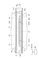
- FIG. 4 schematically shows one aspect of the heating unit HT and the cooling unit CR provided in the processing container 1.
- the processing container 1 shown in FIG. 4 accommodates a heating unit HT, a cooling unit CR, a support unit PP, a support base JD1, a support column JD2, and a wafer W.
- the second wall 1b (second heat insulating layer 1b1) is provided on the second end surface 2b1 of the magnet part 2, and the heating part HT is provided on the second wall 1b.
- the wafer W supported by the support part PP is disposed on the heating part HT, the cooling part CR is provided on the wafer W, and the first wall part 1a (first heat insulating layer 1a1) is provided on the cooling part CR. ) And the first end surface 2a1 of the magnet portion 2 is provided on the first wall portion 1a.
- the processing container 1 shown in FIG. 4 is provided with a gas supply port MU.
- the support base JD1 is supported by the support pillar JD2, and the support pin PA is supported by the support base JD1.
- the cooling unit CR shown in FIG. 4 includes a position PT (arrangement position) where the wafer W is disposed in the processing container 1 and the magnet unit 2 when the wafer W is supported by the support PP in the processing container 1. It arrange
- the cooling unit CR shown in FIG. 4 is provided on the first wall 1 a in the processing container 1.
- a first wall 1a is provided on the cooling part CR.
- the first end surface 2a1 of the magnet portion 2 is disposed on the first wall portion 1a outside the processing container 1.
- the position PT is separated from the cooling unit CR provided on the first wall 1 a side of the processing container 1.
- the heating unit HT shown in FIG. 4 is a resistance heater.
- the heating unit HT is disposed between the position PT and the cooling unit CR.
- the cooling gas supplied from the gas supply device GS is injected into the processing space Sp from the cooling unit CR via the gas supply port unit MU.
- the substrate processing apparatus 10 including the configuration shown in FIG. 4 further includes a moving mechanism MV that moves the wafer W and a power supply DR.
- the moving mechanism MV is driven by electric power supplied from the power supply DR.
- the moving mechanism MV is configured such that the wafer W is parallel to the first end surface 2a1 of the magnet unit 2 and the second end surface 2b1 of the magnet unit 2 in a state where the wafer W is supported by the support unit PP. It moves so that it may approach and separate from the cooling part CR in the wall part 1a side.
- the moving mechanism MV includes an end portion of the support portion PP (an end of the support pin PA in contact with the wafer W) between the first end surface 2a1 of the magnet portion 2 and the second end surface 2b1 of the magnet portion 2.
- the wafer W supported by the support portion PP is made parallel to the first end surface 2a1 of the magnet portion 2 and the second end surface 2b1 of the magnet portion 2 by moving the portion up and down.
- the first end surface 2a1 and the second end surface 2b1 of the magnet unit 2 are moved.
- the wafer W supported by the support part PP has a first end face 2a1 and a second end face between the first end face 2a1 of the magnet part 2 and the second end face 2b1 of the magnet part 2 (position PT). It arrange
- the wafer W in a state of being supported by the support part PP is disposed between the heating part HT and the cooling part CR on the first wall part 1a side. Heating and cooling can be performed effectively. Furthermore, when cooling the wafer W, the wafer W can be brought closer to the cooling unit CR on the first wall portion 1a side, so that the cooling of the wafer W can be performed more effectively. Furthermore, when the wafer W is loaded into the processing space Sp by the transfer robot Rb2, and when the wafer W is unloaded from the processing space Sp by the transfer robot Rb2, the end of the support portion PP is moved to move the wafer W. By adjusting the position, the wafer W can be loaded and unloaded more easily.
- FIG. 5 schematically shows one mode of the heating unit HT and the cooling unit CR provided in the processing container 1.
- the processing container 1 shown in FIG. 5 accommodates a heating unit HT, a cooling unit CR, a support unit PP, a support base JD1, a support column JD2, and a wafer W.
- the second wall 1b (second heat insulating layer 1b1) is provided on the second end face 2b1 of the magnet part 2, and the wafer W supported by the support part PP is the second.
- the heating part HT is provided on the wafer W
- the cooling part CR is provided on the heating part HT
- the first wall part 1a first heat insulating layer
- the processing container 1 shown in FIG. 5 is provided with a gas supply port MU.
- the support base JD1 is supported by the support pillar JD2, and the support pin PA is supported by the support base JD1.
- the cooling unit CR shown in FIG. 5 includes a position PT (arrangement position) where the wafer W is disposed in the processing container 1 and the magnet unit 2 when the wafer W is supported by the support PP in the processing container 1. It arrange
- the cooling unit CR shown in FIG. 5 is provided on the first wall 1a.
- a first wall 1a is provided on the cooling part CR.
- the first end surface 2a1 of the magnet portion 2 is disposed on the first wall portion 1a outside the processing container 1.
- the position PT is separated from the heating unit HT.
- the heating unit HT shown in FIG. 5 is an infrared heater or a lamp heater.
- the heating unit HT is disposed between the position PT and the cooling unit CR.
- the cooling unit CR may be in contact with the heating unit HT and the first wall 1a.
- the cooling gas supplied from the gas supply device GS is injected into the processing space Sp from the cooling unit CR through the gas supply port MU.
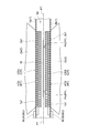
- FIG. 6 schematically illustrates one aspect of the heating unit HT and the cooling unit CR provided in the processing container 1.
- the processing container 1 shown in FIG. 6 accommodates a heating unit HT, a cooling unit CR, a support unit PP, and a wafer W.
- the cooling unit CR illustrated in FIG. 6 includes a first cooling layer CRA and a second cooling layer CRB.
- the heating unit HT shown in FIG. 6 includes a first heating layer HTA and a second heating layer HTB.
- the gas supply port unit MU shown in FIG. 6 includes a first gas supply port MUA and a second gas supply port MUB.
- the second wall 1b (second heat insulating layer 1b1) is provided on the second end face 2b1 of the magnet part 2, and the second cooling layer CRB is provided on the second wall 1b.
- the second heating layer HTB is provided on the second cooling layer CRB
- the wafer W supported by the support portion PP is disposed on the second heating layer HTB
- the first heating layer HTB is disposed on the wafer W.
- the heating layer HTA is provided
- the first cooling layer CRA is provided on the first heating layer HTA
- the first wall portion 1a (first heat insulating layer 1a1) is provided on the first cooling layer CRA.
- the first end face 2a1 of the magnet part 2 is provided on the first wall part 1a.
- the processing container 1 shown in FIG. 6 is provided with a gas supply port MU.
- the first cooling layer CRA has a position PT (where the wafer W is disposed in the processing container 1 when the wafer W is supported by the support portion PP in the processing container 1. (Positioning position) and the first end surface 2a1 of the magnet part 2 are arranged.
- the second cooling layer CRB is disposed in the processing container 1 between the position PT and the second end face 2 b 1 of the magnet unit 2.
- the first heating layer HTA is an infrared heater or a lamp heater. In the processing container 1 shown in FIG. 6, the first heating layer HTA is disposed between the position PT and the first cooling layer CRA. In the processing container 1 shown in FIG. 6, the second heating layer HTB is an infrared heater or a lamp heater. In the processing container 1 shown in FIG. 6, the second heating layer HTB is disposed between the position PT and the second cooling layer CRB.
- the first cooling layer CRA is disposed between the first wall portion 1a and the first heating layer HTA.
- the first cooling layer CRA may be in contact with the first wall 1a and the first heating layer HTA.
- the second cooling layer CRB is disposed between the second wall 1b and the second heating layer HTB.
- the second cooling layer CRB may be in contact with the second wall 1b and the second heating layer HTB.
- the position PT is separated from the first heating layer HTA and the second heating layer HTB.
- the cooling gas supplied from the gas supply device GS is injected from the first cooling layer CRA into the processing space Sp via the first gas supply port MUA, and the second The gas is injected from the second cooling layer CRB into the processing space Sp through the gas supply port MUB.
- the heating and cooling of the wafer W can be sufficiently performed in a shorter period of time, and the heating of the wafer W can be performed.
- the cooling is performed sequentially, the wafer W after heating can be more effectively cooled.
- the wafer W may be processed by the following steps ST1 to ST5 shown in FIG. First, the wafer W is loaded into the processing container 1 via the gate valve RA, and the wafer W is placed at a position PT (see FIGS. 4 to 6) in the processing container 1 (step ST1).
- step ST2 the wafer W is heated to a predetermined temperature (hereinafter, “predetermined” indicates that it is preset) using the heating unit HT.
- predetermined indicates that it is preset
- the heating unit HT is the resistance heater shown in FIG. 4, the heating unit HT is always heated, and heating by the heating unit HT is started from the timing when the wafer W is placed on the heating unit HT.
- the heating unit HT is the infrared heater or the lamp heater shown in FIGS. 5 and 6, after the wafer W is arranged at the position PT in the processing container 1, the heating unit HT is turned on and the wafer is set with a preset power. Heat W.
- step ST3 following step ST2, the temperature of the wafer W is held at a predetermined temperature for a predetermined time.
- the temperature of the wafer W held in step ST3 is 300 to 500 ° C., and the time for holding the wafer W at the temperature in step ST3 is 1 [sec] to 10 [min].
- step ST4 following step ST3, the wafer W is cooled.
- the wafer W is cooled at a cooling rate of 0.5 [° C./sec] or more.
- the cooling rate can be controlled by the flow rate of the cooling gas and the pressure in the processing container 1.
- the cooling rate can be increased as the flow rate of the cooling gas is increased and the pressure in the processing container 1 is increased.
- step ST4 the wafer W is heated by the support pins PA and the heating stage shown in FIG.
- the heating unit HT itself may be said to be a heating stage.
- the wafer W may be cooled in a state of being separated from the stage. .
- step ST2 and step ST3 position of wafer W placed on the heating stage shown in FIG. 4
- the wafer W is separated from the heating stage by the support pins PA in step ST4. Then, the wafer W may be cooled.
- the position of the wafer W in step ST4 may be a position PT shown in FIG.
- the cooling in step ST4 is performed by flowing the cooling gas from the cooling unit CR after turning off the power of the heating unit HT. obtain.
- step ST5 subsequent to step ST4, the wafer W is unloaded from the processing chamber 1 through the gate valve RA.
- the unloading of the wafer W in step ST5 can be started when the temperature of the wafer W becomes equal to or lower than the temperature at which the wafer W can be unloaded.
- the time required for cooling the wafer W can be a time determined in advance by measurement.
- second gas supply port MV ... moving mechanism, OC ... characteristic measuring device, OM ... opening, OMP ... notch, PA ... support pin, PP ... Support section, PT ... position, RA ... gate valve, Rb1 ... transfer robot, Rb2 ... transfer robot, Sp ... processing space, TU ... chiller unit, W ... wafer.
Landscapes
- Chemical & Material Sciences (AREA)
- Engineering & Computer Science (AREA)
- Mechanical Engineering (AREA)
- Materials Engineering (AREA)
- Metallurgy (AREA)
- Organic Chemistry (AREA)
- Chemical Kinetics & Catalysis (AREA)
- Physics & Mathematics (AREA)
- Manufacturing & Machinery (AREA)
- Thermal Sciences (AREA)
- General Engineering & Computer Science (AREA)
- Power Engineering (AREA)
- Electromagnetism (AREA)
- Crystallography & Structural Chemistry (AREA)
- Hall/Mr Elements (AREA)
- Mram Or Spin Memory Techniques (AREA)
- Container, Conveyance, Adherence, Positioning, Of Wafer (AREA)
- Physical Vapour Deposition (AREA)
- Health & Medical Sciences (AREA)
- High Energy & Nuclear Physics (AREA)
- Toxicology (AREA)
- Robotics (AREA)
Abstract
一実施形態における基板処理装置(10)および処理システム(100)は,磁性層を有する基板(W)を枚葉に処理し,基板を支持する支持部(PP)と支持部に支持される基板を加熱する加熱部(HT)と支持部に支持される基板を冷却する冷却部(CR)と磁界を発生させる磁石部(2)と,支持部,加熱部,および冷却部を収容する処理容器(1)とを備え,磁石部は互いに並行に延びている第1の端面(2a1)と第2の端面(2b1)とを備え,第1の端面と第2の端面とは離間して向かい合い,第1の端面は磁石部の第1の磁極に対応し,第2の端面は磁石部の第2の磁極に対応し,処理容器は第1の端面と第2の端面との間に配置される。
Description
本発明の実施形態は、基板処理装置および処理システムに関するものである。
MRAM(Magnetoresistive Random Access Memory)の製造工程において、枚葉式のPVD(physical vapor deposition)成膜装置を用いて成膜した後のMTJ(Magnetic Tunnel Junction)素子に対しては着磁処理およびアニール処理等が施される。特許文献1には、成膜処理後に高い真空度を維持したまま基板のみを急速に加熱し、かつ急速に冷却すること目的とした真空加熱冷却装置に係る技術が開示されている。特許文献2には、半導体ウエハへの不純物の付着を低減することを目的とした磁気アニール装置に係る技術が開示されている。
MRAMの製造工程において枚葉式のPVD成膜装置から成膜後に順次取り出された複数のMTJ素子は、一括して、PVD成膜装置とは別の装置に搬送され当該装置内において着磁処理およびアニール処理が行われた後に、個々のMTJ素子ごとに、CIPT(Current-In-Plane Tunneling)測定器等を用いてMTJ素子に対する特性評価(磁気抵抗比等)が行われる。この場合、この特性評価の結果によって製造工程での不具合の発生の可能性が見い出されても、当該特性評価は複数のMTJ素子が一括して着磁処理およびアニール処理された後に行われるので、これら複数のMTJ素子は不具合が生じた可能性のある製造工程で製造されたものとして扱われ得る。従って、MRAMの製造工程において成膜後に着磁処理およびアニール処理を枚葉で行い得る基板処理装置および処理システムの提供が望まれている。
一態様においては、基板処理装置が提供される。この基板処理装置は、磁性層を有する基板を枚葉に処理する基板処理装置であって、基板を支持する支持部と、支持部に支持される基板を加熱する加熱部と、支持部に支持される基板を冷却する冷却部と、支持部、加熱部、および冷却部を収容する処理容器と、磁界を発生させる磁石部と、を備え、磁石部は、互いに並行に延びている第1の端面と第2の端面とを備え、第1の端面と第2の端面とは、離間して向かい合い、第1の端面は、磁石部の第1の磁極に対応し、第2の端面は、磁石部の第2の磁極に対応し、処理容器は、第1の端面と第2の端面との間に配置される。
上記の一態様では、磁性層を有する基板に対する着磁処理およびアニール処理に必要な磁石部と基板の支持部と加熱部と冷却部とが基板を枚葉に処理する一の基板処理装置に設けられているので、当該基板に対する着磁処理およびアニール処理が基板毎に枚葉に行え得る。従って、上記の一態様では、例えばMRAMの製造工程等において、成膜後に着磁処理およびアニール処理を枚葉で行い得る。
一実施形態では、基板が支持部によって支持されている状態において、基板は、第1の端面および第2の端面から見て第1の端面内および第2の端面内に含まれ、第1の端面および第2の端面に対して並行に延びる。従って、磁石部において第1の端面と第2の端面との間に生じる磁力線は、支持部によって支持されている状態の基板が延びている方向に対して垂直(基板に対し面直)となり得る。
一実施形態では、冷却部は、処理容器内において、基板が支持部によって支持されている場合に基板が処理容器内に配置される位置(配置位置という)と第1の端面との間に配置され、加熱部は、配置位置と冷却部との間に配置される。このように、支持部によって支持されている状態の基板は加熱部と冷却部との間に配置されるので、基板に対する加熱および冷却が効果的に行われ得る。
一実施形態では、基板を移動させる移動機構を更に備える。移動機構は、基板が支持部によって支持されている状態において、基板を、第1の端面と第2の端面とに対して平行としつつ冷却部に接近および離間するように、移動させる。従って、基板への冷却時には、基板を、冷却部に対してより接近させることができるので、基板に対する冷却がより効果的に行われ得る。
一実施形態では、冷却部は、処理容器内において、基板が支持部によって支持されている場合に基板が処理容器内に配置される位置(配置位置という)と第1の端面との間に配置され、加熱部は、配置位置と冷却部との間に配置される。このように、加熱と冷却とが基板の同一の表面に対して行われるので、基板に対し加熱、冷却が順次行われる場合に、加熱後の基板に対する冷却がより効果的に行われ得る。
一実施形態では、加熱部は、第1の加熱層と第2の加熱層とを備える。冷却部は、第1の冷却層と第2の冷却層とを備える。第1の冷却層は、処理容器内において、基板が支持部によって支持されている場合に基板が処理容器内に配置される位置(配置位置という)と第1の端面との間に配置され、第2の冷却層は、処理容器内において、配置位置と第2の端面との間に配置される。第1の加熱層は、配置位置と第1の冷却層との間に配置され、第2の加熱層は、配置位置と第2の冷却層との間に配置される。このように、基板の二つの表面のそれぞれに対して加熱と冷却とが行われるので、基板に対する加熱および冷却がより短期間で十分に行われ得ると共に、基板に対し加熱、冷却が順次行われる場合に、加熱後の基板に対する冷却がより効果的に行われ得る。
一態様においては、処理システムが提供される。この処理システムは、複数の成膜装置と、上記態様および上記実施形態の何れかに係る基板処理装置と、測定装置と、を備える。成膜装置は、磁性層を有する基板を形成し、基板処理装置は、成膜装置によって形成された基板を枚葉に処理し、測定装置は、成膜装置によって形成された基板、および、基板処理装置によって処理された後の基板に対して電磁気的特性値を枚葉に測定する。この一態様では、磁性層を有する基板に対する着磁処理およびアニール処理に必要な磁石部と基板の支持部と加熱部と冷却部とが基板を枚葉に処理する一の基板処理装置に設けられているので、当該基板に対する着磁処理およびアニール処理が基板毎に枚葉に行え得ると共に、成膜装置によって形成された基板、および、上記した着磁処理およびアニール処理の後の基板に対する電磁気的特性値の測定が、枚葉に行い得る。
一実施形態では、大気搬送室を更に備え、測定装置は大気搬送室に連結される。このように、測定装置が、処理システムの大気搬送室を介して設置可能となるので、測定装置の設置場所に対する制約が低減され、よって測定装置の設置が容易に行われ得る。
一実施形態では、電磁気的特性値は、磁気抵抗比である。このように、基板の磁気抵抗比を測定することによって、基板の電磁気的な特性が良好に評価し得る。
以上説明したように、MRAMの製造工程において成膜後に着磁処理およびアニール処理を枚葉で行い得る基板処理装置および処理システムが提供される。
以下、図面を参照して種々の実施形態について詳細に説明する。なお、各図面において同一または相当の部分に対しては同一の符号を附すこととする。図1は、一実施形態に係る基板処理装置10の主要な構成の一例を示す図である。基板処理装置10は、MRAMの製造に用いられ、磁性層を有する基板(以下、ウエハWという場合がある)に形成されるMTJ素子(例えばMgO/CoFeB積層膜を有する素子)の成膜後に、着磁処理およびアニール処理を行う装置である。基板処理装置10は、後述する図2に示す処理システム100に設けられて利用され得る。
基板処理装置10は、基板処理装置10、磁石部2、電源EF、素線部3a、素線部3b、ヨーク4、冷却部CR、加熱部HT、電源ES、ガス供給装置GS、ゲートバルブRA、チラーユニットTU、支持部PP(三つ以上の支持ピンPAを含んでおり、以下同様)を備える。処理容器1は、ウエハW(基板)を処理する処理空間Spを画定する。処理容器1は、第1の壁部1a、第2の壁部1b、排気管1cを備える。処理容器1は、支持部PP、加熱部HT、冷却部CRを収容する。
第1の壁部1aは、第1の断熱層1a1を備える。第2の壁部1bは、第2の断熱層1b1を備える。磁石部2は、第1のコア部2a、第2のコア部2bを備える。第1のコア部2aは、第1の端面2a1を備える。第2のコア部2bは、第2の端面2b1を備える。
処理容器1内において、ウエハWは、支持部PPによって支持される。ウエハWは、図2に示す搬送ロボットRb2によってトランスファーチャンバ121からゲートバルブRAを介して処理容器1の処理空間Spに搬入され、支持部PPによって支持されるように配置される。ウエハWは、処理空間Sp内において支持部PPによって支持されている状態において、磁石部2の第1のコア部2aの第1の端面2a1および磁石部2の第2のコア部2bの第2の端面2b1から見て、第1の端面2a1内および第2の端面2b1内に含まれ(覆われ)、第1の端面2a1および第2の端面2b1に対して並行に延びている。基板処理装置10が処理システム100に設置されている場合、ウエハWは、処理空間Sp内において支持部PPによって支持されている状態において、鉛直方向に対して垂直に延びる。
磁石部2は、電磁石であり、電源EFから素線部3aおよび素線部3bに電流が供給されることによって磁界を発生し得る。素線部3aは、第1のコア部2aの周りに巻き回され被覆された銅線等であり、素線部3bは、第2のコア部2bの周りに巻き回され被覆された銅線等である。第1の端面2a1は、磁石部2の第1の磁極に対応し、第2の端面2b1は、磁石部2の第2の磁極に対応している。第1の磁極、第2の磁極のそれぞれは、例えば、N極、S極であり得る。第1の端面2a1と第2の端面2b1とは、互いに並行に延びており、離間して向かい合っている。第1のコア部2aの周囲には、素線部3aが設けられ、第2のコア部2bの周囲には素線部3bが設けられている。第1のコア部2aおよび第2のコア部2bは、例えば鉄等の金属からなり、素線部3a、素線部3bによって生じる磁力線を第1の端面2a1および第2の端面2b1に収束させる。処理容器1は、磁石部2の第1の端面2a1と磁石部2の第2の端面2b1との間に配置される。磁石部2の第1のコア部2a(第1の端面2a1)は、処理容器1の外側において処理容器1の第1の壁部1a上に設けられ、磁石部2の第2のコア部2b(第2の端面2b1)は、処理容器1の外側において処理容器1の第2の壁部1b上に設けられる。第1の壁部1aは、第1の端面2a1に接していても良い。第2の壁部1bは、第2の端面2b1に接していても良い。
第1の断熱層1a1は、第1の壁部1aの内部に設けられている。第1の断熱層1a1は、例えば、第1の壁部1aの内部に設けられた水冷ジャケットである。第1の断熱層1a1は、第1の端面2a1に接していても良い。第2の断熱層1b1は、第2の壁部1bの内部に設けられている。第2の断熱層1b1は、例えば第2の壁部1bの内部に設けられた水冷ジャケットである。第2の断熱層1b1は、第2の端面2b1に接していても良い。第1の断熱層1a1の水冷ジャケットおよび第2の断熱層1b1の水冷ジャケットは、何れも、チラーユニットTUに接続された配管を有している。チラーユニットTUは、この配管(第1の断熱層1a1および第2の断熱層1b1)に冷却液を循環させることによって、処理容器1と磁石部2との間の熱の移動を低減する(断熱する)。第1の断熱層1a1および第2の断熱層1b1は、例えば繊維系や発泡系の断熱材を有していても良く、この場合、この断熱材は、第1の壁部1aと第1のコア部2aの第1の端面2a1との間、および、第2の壁部1bと第2のコア部2bの第2の端面2b1との間に設置され得る。
基板処理装置10が処理システム100に設置されている場合、第1の端面2a1と第2の端面2b1とは鉛直方向に対して垂直に延びており、第1の端面2a1は第2の端面2b1に対して鉛直上方にある。
処理空間Sp内において支持部PPによって支持されている状態のウエハWから見て、ウエハWは、第1の端面2a1内および第2の端面2b1内に含まれている(覆われている)。換言すれば、磁石部2の第1のコア部2aからみて、このウエハWは第1の端面2a1内に含まれており(覆われており)、磁石部2の第2のコア部2bからみて、このウエハWは第2の端面2b1内に含まれている(覆われている)。磁石部2によって発生される磁力線は、処理空間Sp内において支持部PPによって支持されている状態のウエハWに対し垂直となる。ウエハWには、磁石部2によって、0.1~2[T]程度の磁界が生じ得る。
加熱部HTは、支持部PPによって支持されるウエハWを加熱する。加熱部HTは、例えば、抵抗加熱ヒータ、赤外線ヒータまたはランプヒータ等であり得る。加熱部HTは、電源ESによって供給される電力によってヒータとして機能する。加熱部HTは、第1の壁部1aおよび第2の壁部1bからみて、支持部PPによって支持されているウエハWの全体を覆って(含んで)おり、ウエハW(ウエハWの表面および/または裏面)の全体に対して加熱し得る構成を有する。
冷却部CRは、ガス供給装置GSから供給される冷却ガスを処理空間Sp内に噴射する。冷却部CRは、少なくとも処理容器1内において処理容器1の第1の壁部1aに設けられている部分を有している。冷却ガスは、N2ガスまたはHeガスなどの希ガスであり得る。冷却部CRは、第1の壁部1aおよび第2の壁部1bからみて、支持部PPによって支持されているウエハWの全体を覆って(含んで)おり、ウエハW(ウエハWの表面および/または裏面)の全体に対して冷却し得る構成を有する。ウエハWの冷却に用いられた冷却ガスは、処理空間Spに連通する排気管1cから外部に排気される。排気管1cには、図示しない排気ポンプが設けられている。
加熱部HTに電力を供給する電源ES、冷却部CRに冷却ガスを供給するガス供給装置GS、磁石部2に電力を供給する電源EF、第1の断熱層1a1および第2の断熱層1b1に冷却液を循環させるチラーユニットTUの駆動制御は、後述の処理システム100が備える制御部Cntによって行われる。制御部Cntは、更に、ゲートバルブRAの開閉機構(後述の図4に示す構成の場合、移動機構MVおよび電源DRを更に含む)を制御する。
上記した基板処理装置10では、磁性層を有するウエハWに対する着磁処理およびアニール処理に必要な磁石部2と支持部PPと加熱部HTと冷却部CRとが基板を枚葉に処理する一の基板処理装置10に設けられているので、ウエハWに対する着磁処理およびアニール処理がウエハ毎に枚葉に行え得る。従って、この基板処理装置10では、MRAMの製造工程において、成膜後に着磁処理およびアニール処理を枚葉で行い得る。更に、磁石部2において、磁石部2の第1の端面2a1と磁石部2の第2の端面2b1との間に生じる磁力線は、支持部PPによって支持されている状態のウエハWが延びている方向に対して垂直(基板に対し面直)となり得る。
図1に示す処理容器1は、図2に示す処理システム100の複数の処理室100aのうち何れか一の処理室100aに収容されている。図2は、図1に示す基板処理装置10を備える処理システム100の主要な構成の一例を示す図である。複数の処理室100aのうち基板処理装置10が収容されている処理室100aを除く他の処理室100aでは、例えば、PVD(Physical Vapor Deposition)による金属材料の成膜や金属膜の酸化処理などの様々な処理が行われ得る。
処理システム100は、台122a、台122b、台122c、台122d、収容容器124a、収容容器124b、収容容器124c、収容容器124d、ローダモジュールLM、搬送ロボットRb1、制御部Cnt、特性値測定装置OC、ロードロックチャンバLL1、ロードロックチャンバLL2、ゲートGA1、ゲートGA2を備える。処理システム100は、更に、複数のトランスファーチャンバ121、複数の処理室100a、複数のゲートGB1、複数のゲートGB2を備える。トランスファーチャンバ121は、搬送ロボットRb2を備える。
ロードロックチャンバLL1と、ロードロックチャンバLL1に接しているトランスファーチャンバ121との間にはゲートGA1が設けられており、ゲートGA1を介して、ウエハWが、ロードロックチャンバLL1と、ロードロックチャンバLL1に接しているトランスファーチャンバ121との間を、搬送ロボットRb2によって移動する。ロードロックチャンバLL2と、ロードロックチャンバLL2に接しているトランスファーチャンバ121との間にはゲートGA2が設けられており、ゲートGA2を介して、ウエハWが、ロードロックチャンバLL2と、ロードロックチャンバLL2に接しているトランスファーチャンバ121との間を、搬送ロボットRb2によって移動する。
互いに隣り合う二つのトランスファーチャンバ121間には、ゲートGB1が設けられており、ゲートGB1を介して、当該二つのトランスファーチャンバ121の間を、搬送ロボットRb2によって移動する。処理室100aと、この処理室100aに接しているトランスファーチャンバ121との間にはゲートGB2が設けられており、ゲートGB2を介して、処理室100aと、この処理室100aに接するトランスファーチャンバ121との間を、搬送ロボットRb2によって移動する。
台122a~122dは、ローダモジュールLMの一縁に沿って配列されている。台122a~122dのそれぞれの上には、収容容器124a~124dがそれぞれ設けられている。収容容器124a~124d内には、ウエハWが収容され得る。
ローダモジュールLM内には、搬送ロボットRb1が設けられている。搬送ロボットRb1は、収容容器124a~124dの何れかに収容されているウエハWを取り出して、ウエハWを、ロードロックチャンバLL1またはLL2に搬送する。
ロードロックチャンバLL1およびLL2は、ローダモジュールLMの別の一縁に沿って設けられており、ローダモジュールLMに接続されている。ロードロックチャンバLL1およびロードロックチャンバLL2は、予備減圧室を構成している。ロードロックチャンバLL1およびロードロックチャンバLL2は、それぞれ、ゲートGA1、ゲートGA2を介して、トランスファーチャンバ121に接続されている。
トランスファーチャンバ121は、減圧可能なチャンバであり、トランスファーチャンバ121内には搬送ロボットRb2が設けられている。トランスファーチャンバ121には、基板処理装置10が接続されている。搬送ロボットRb2は、ロードロックチャンバLL1またはロードロックチャンバLL2から、それぞれゲートGA1、ゲートGA2を介してウエハWを取り出して、当該ウエハWを基板処理装置10に搬送する。
処理システム100は、特性値測定装置OCを更に備える。特性値測定装置OCは処理システム100の大気搬送室(ローダモジュールLMを含む)に連結されても良い。図2に示す一実施形態においては、特性値測定装置OCはローダモジュールLMに接続される。特性値測定装置OCは、処理システム100の複数の成膜装置(複数の処理室100aのうち成膜処理を行う複数の処理室100a)によって形成された磁性層を有するウエハW、および、基板処理装置10によって処理された後のウエハWに対して、電磁気的特性値を枚葉に測定する。特性値測定装置OCは、例えば、磁気抵抗比等の電磁気的特性値を測定可能なCIPT(Current-In-Plane Tunneling)測定器であり得る。ウエハWは、搬送ロボットRb1および搬送ロボットRb2によって、特性値測定装置OCと基板処理装置10との間で移動され得る。搬送ロボットRb1によってウエハWが特性値測定装置OC内に収容され、特性値測定装置OC内においてウエハWの位置合わせが行われた後に、特性値測定装置OCは、ウエハWの特性(例えば磁気抵抗比等)を測定し、測定結果を制御部Cntに送信する。
制御部Cntは、プロセッサ、記憶部、入力装置、表示装置等を備えるコンピュータであり、処理システム100の各部を制御する。制御部Cntは、搬送ロボットRb1、搬送ロボットRb2、特性値測定装置OC、複数の処理室100aのそれぞれに格納されている各種装置(例えば、基板処理装置10)等に接続されており、更に、基板処理装置10においては、電源ES、電源EF(図4に示す構成の場合、電源DRを更に含む)、ガス供給装置GS、チラーユニットTU、ゲートバルブRAの開閉機構、および支持部PP(支持ピンPA)を上下動作させる移動機構MV等に接続されている。制御部Cntは、処理システム100の各部を制御するためのコンピュータプログラム(入力されたレシピに基づくプログラム)に従って動作し、制御信号を送出する。制御部Cntからの制御信号によって、処理システム100の各部、例えば、搬送ロボットRb1,Rb2、特性値測定装置OC、および、基板処理装置10の各部を制御する。制御部Cntの記憶部には、処理システム100の各部を制御するためのコンピュータプログラム、および、当該プログラムの実行に用いられる各種のデータが、読出し自在に格納されている。
上記した一実施形態に係る処理システム100では、複数の処理室100aのうち何れか二つ以上の処理室100a(複数の成膜装置に該当)で行われる成膜処理と、複数の処理室100aの何れか一の処理室100aに設けられた基板処理装置10によって行われる成膜後の磁化アニール処理と、特性値測定装置OCによって行われる測定であって成膜処理および磁化アニール処理後のウエハWに対する磁気抵抗比等の特性値の測定とが、枚葉に行える。
基板処理装置10のヨーク4の形状を図3の(a)部および(b)部に示す。図1に示す基板処理装置10のヨーク4の二種類の形状のそれぞれが図3の(a)部および図3の(b)部に例示されている。
図3の(a)部に示されているヨーク4は、ヨーク4の中央部にヨーク4の側面を貫通する開口部OMが設けられている。処理容器1、磁石部2、素線部3a、素線部3bは、図3の(a)部に示す開口部OM内に収容されている。図3の(a)部に示す開口部OMは、図2に示す処理システム100のゲートGB2と向かい合う位置に配置されている。図3の(a)部に示す開口部OMには、ゲートGB2と向かい合う側に切欠部OMPが設けられている。ゲートGB2と向かい合う位置に設けられた開口部OMおよび切欠部OMPによって、処理システム100のトランスファーチャンバ121から処理容器1内へのウエハWの搬入が容易となる。
図3の(b)部に示されているヨーク4は、ヨーク4の側面に開口部OMが設けられており、図3の(b)部に示す開口部OMは、ヨーク4の側面における凹部となっている。処理容器1、磁石部2、素線部3a、素線部3bは、図3の(b)部に示す開口部OM内に収容されている。図3の(b)部に示す開口部OMは、図2に示す処理システム100のゲートGB2と向かい合う位置に配置されている。ゲートGB2と向かい合う位置に設けられた図3の(b)部に示す開口部OMによって、処理システム100のトランスファーチャンバ121から処理容器1内へのウエハWの搬入が容易となる。
次に、図4~図6を参照して、処理容器1内に設けられる加熱部HTおよび冷却部CRの具体的な態様について説明する。図4には、処理容器1内に設けられる加熱部HTおよび冷却部CRの一態様が模式的に示されている。図4に示す処理容器1には、加熱部HT、冷却部CR、支持部PP、支持台JD1、支持柱JD2、ウエハWが収容されている。図4に示す構成においては、磁石部2の第2の端面2b1上に第2の壁部1b(第2の断熱層1b1)が設けられ、第2の壁部1b上に加熱部HTが設けられ、支持部PPによって支持されているウエハWが加熱部HT上に配置され、ウエハW上に冷却部CRが設けられ、冷却部CR上に第1の壁部1a(第1の断熱層1a1)が設けられ、第1の壁部1a上に磁石部2の第1の端面2a1が設けられている。図4に示す処理容器1には、ガス供給口部MUが設けられている。支持台JD1は、支持柱JD2によって支持されており、支持ピンPAは、支持台JD1によって支持されている。
図4に示す冷却部CRは、処理容器1内において、ウエハWが支持部PPによって支持されている場合にウエハWが処理容器1内に配置される位置PT(配置位置)と磁石部2の第1のコア部2aの第1の端面2a1との間に配置される。図4に示す冷却部CRは、処理容器1内において第1の壁部1aに設けられている。冷却部CR上に第1の壁部1aが設けられている。処理容器1の外側において第1の壁部1aに磁石部2の第1の端面2a1が配置されている。図4に示す構成において、位置PTは、処理容器1の第1の壁部1a側に設けられている冷却部CRに対し離間している。図4に示す加熱部HTは、抵抗加熱ヒータである。加熱部HTは、位置PTと冷却部CRとの間に配置される。
図4に示す構成において、ガス供給装置GSから供給される冷却ガスは、ガス供給口部MUを介して冷却部CRから処理空間Sp内に噴射される。
図4に示す構成を含む基板処理装置10は、ウエハWを移動させる移動機構MVと電源DRとを更に備える。移動機構MVは、電源DRによって供給される電力によって駆動する。移動機構MVは、ウエハWが支持部PPによって支持されている状態において、ウエハWを、磁石部2の第1の端面2a1と磁石部2の第2の端面2b1とに対し平行としつつ第1の壁部1a側にある冷却部CRに接近および離間するように移動させる。より具体的には、移動機構MVは、磁石部2の第1の端面2a1と磁石部2の第2の端面2b1との間において支持部PPの端部(ウエハWと接する支持ピンPAの端部)を上下させることによって、支持部PPによって支持されているウエハWを、磁石部2の第1の端面2a1と磁石部2の第2の端面2b1とに対し平行としつつ、磁石部2の第1の端面2a1と磁石部2の第2の端面2b1との間を移動させる。支持部PPによって支持されているウエハWは、磁石部2の第1の端面2a1と、磁石部2の第2の端面2b1との間(位置PT)において、第1の端面2a1と第2の端面2b1とに平行となるように配置されており、この位置から、移動機構MVによって、第1の端面2a1側に設けられている冷却部CRに向けて移動可能となっている。
図4に示す構成では、支持部PPによって支持されている状態のウエハWは加熱部HTと、第1の壁部1aの側にある冷却部CRとの間に配置されるので、ウエハWに対する加熱および冷却が効果的に行われ得る。更に、ウエハWへの冷却時には、ウエハWを、第1の壁部1aの側にある冷却部CRに対してより接近させることができるので、ウエハWに対する冷却がより効果的に行われ得る。更に、搬送ロボットRb2によってウエハWが処理空間Sp内に搬入される場合、搬送ロボットRb2によってウエハWが処理空間Spから搬出される場合には、支持部PPの端部を移動させてウエハWの位置を調整することによって、ウエハWの搬入および搬出をより容易に行い得るようにできる。
図5には、処理容器1内に設けられる加熱部HTおよび冷却部CRの一態様が模式的に示されている。図5に示す処理容器1には、加熱部HT、冷却部CR、支持部PP、支持台JD1、支持柱JD2、ウエハWが収容されている。図5に示す構成においては、磁石部2の第2の端面2b1上に第2の壁部1b(第2の断熱層1b1)が設けられ、支持部PPによって支持されているウエハWが第2の壁部1b上に配置され、このウエハW上に加熱部HTが設けられ、加熱部HT上に冷却部CRが設けられ、冷却部CR上に第1の壁部1a(第1の断熱層1a1)が設けられ、第1の壁部1a上に磁石部2の第1の端面2a1が設けられている。図5に示す処理容器1には、ガス供給口部MUが設けられている。支持台JD1は、支持柱JD2によって支持されており、支持ピンPAは、支持台JD1によって支持されている。
図5に示す冷却部CRは、処理容器1内において、ウエハWが支持部PPによって支持されている場合にウエハWが処理容器1内に配置される位置PT(配置位置)と磁石部2の第1の端面2a1との間に配置される。図5に示す冷却部CRは、第1の壁部1aに設けられている。冷却部CR上に第1の壁部1aが設けられている。処理容器1の外側において第1の壁部1aに磁石部2の第1の端面2a1が配置されている。図5に示す処理容器1において、位置PTは、加熱部HTに対し離間している。図5に示す加熱部HTは、赤外線ヒータまたはランプヒータである。加熱部HTは、位置PTと冷却部CRとの間に配置される。冷却部CRは、加熱部HTと第1の壁部1aとに接する場合がある。
図5に示す処理容器1において、ガス供給装置GSから供給される冷却ガスは、ガス供給口部MUを介して冷却部CRから処理空間Sp内に噴射される。
図5に示す構成では、加熱と冷却とがウエハWの同一の表面に対して行われるので、ウエハWに対し加熱、冷却が順次行われる場合に、加熱後のウエハWに対する冷却がより効果的に行われ得る。
図6には、処理容器1内に設けられる加熱部HTおよび冷却部CRの一態様が模式的に示されている。図6に示す処理容器1には、加熱部HT、冷却部CR、支持部PP、ウエハWが収容されている。図6に示す冷却部CRは、第1の冷却層CRAと第2の冷却層CRBとを備える。図6に示す加熱部HTは、第1の加熱層HTAと第2の加熱層HTBとを備える。図6に示すガス供給口部MUは、第1のガス供給口MUAと第2のガス供給口MUBとを備える。
図6に示す構成において、磁石部2の第2の端面2b1上に第2の壁部1b(第2の断熱層1b1)が設けられ、第2の壁部1b上に第2の冷却層CRBが設けられ、第2の冷却層CRB上に第2の加熱層HTBが設けられ、支持部PPによって支持されているウエハWが第2の加熱層HTB上に配置され、ウエハW上に第1の加熱層HTAが設けられ、第1の加熱層HTA上に第1の冷却層CRAが設けられ、第1の冷却層CRA上に第1の壁部1a(第1の断熱層1a1)が設けられ、第1の壁部1a上に磁石部2の第1の端面2a1が設けられている。図6に示す処理容器1には、ガス供給口部MUが設けられている。
図6に示す処理容器1において、第1の冷却層CRAは、処理容器1内において、ウエハWが支持部PPによって支持されている場合にウエハWが処理容器1内に配置される位置PT(配置位置)と磁石部2の第1の端面2a1との間に配置されている。図6に示す処理容器1において、第2の冷却層CRBは、処理容器1内において、位置PTと磁石部2の第2の端面2b1との間に配置されている。
図6に示す処理容器1において、第1の加熱層HTAは、赤外線ヒータまたはランプヒータである。図6に示す処理容器1において、第1の加熱層HTAは、位置PTと第1の冷却層CRAとの間に配置されている。図6に示す処理容器1において、第2の加熱層HTBは、赤外線ヒータまたはランプヒータである。図6に示す処理容器1において、第2の加熱層HTBは、位置PTと第2の冷却層CRBとの間に配置されている。
図6に示す処理容器1において、第1の冷却層CRAは、第1の壁部1aと第1の加熱層HTAとの間に配置される。第1の冷却層CRAは、第1の壁部1aと第1の加熱層HTAとに接しても良い。図6に示す処理容器1において、第2の冷却層CRBは、第2の壁部1bと第2の加熱層HTBとの間に配置される。第2の冷却層CRBは、第2の壁部1bと第2の加熱層HTBとに接しても良い。図6に示す処理容器1において、位置PTは、第1の加熱層HTAと第2の加熱層HTBとに対し離間している。
図6に示す処理容器1において、ガス供給装置GSから供給される冷却ガスは、第1のガス供給口MUAを介して第1の冷却層CRAから処理空間Spに噴射されると共に、第2のガス供給口MUBを介して第2の冷却層CRBから処理空間Sp内に噴射される。
図6に示す構成では、ウエハWの二つの表面のそれぞれに対して加熱と冷却とが行われるので、ウエハWに対する加熱および冷却がより短期間で十分に行われ得ると共に、ウエハWに対し加熱、冷却が順次行われる場合に、加熱後のウエハWに対する冷却がより効果的に行われ得る。
次に、図7に示す処理動作について説明する。一実施形態において、ウエハWは、図7に示す下記のステップST1~ST5によって処理され得る。まず、ゲートバルブRAを介してウエハWを処理容器1内に搬入し、処理容器1内の位置PT(図4~図6を参照)にウエハWを配置する(ステップST1)。
ステップST1に引き続くステップST2において、加熱部HTを用いて所定(以下、所定とは、予め設定されていることを示す)の温度にウエハWを加熱する。加熱部HTが図4に示す抵抗加熱ヒータの場合には、加熱部HTは常時加熱されており、加熱部HT上にウエハWが載置されたタイミングから、加熱部HTによる加熱が開始される。加熱部HTが図5および図6に示す赤外線ヒータまたはランプヒータの場合には、ウエハWを処理容器1内の位置PTに配置した後に、加熱部HTをONにし、予め設定されたパワーによってウエハWを加熱する。
ステップST2に引き続くステップST3において、ウエハWの温度を、所定時間の間、所定の温度に保持する。ステップST3において保持されるウエハWの温度は、300~500℃であり、ステップST3においてウエハWを当該温度に保持する時間は、1[sec]~10[min]である。
ステップST3に引き続くステップST4において、ウエハWを冷却する。ステップST4においてウエハWに対する冷却は、0.5[℃/sec]以上の冷却速度で行う。冷却速度は、冷却ガスの流量と処理容器1内の圧力とによって制御され得る。冷却ガスの流量が多いほど、また処理容器1内の圧力が高いほど、冷却速度は大きくなり得る。
加熱部HTが図4に示す抵抗加熱ヒータの場合には、ステップST3の終了後に、ステップST4において、ウエハWを支持ピンPAによって図4に示す加熱ステージ(加熱部HTを内蔵しておりウエハWが載置され得るステージであり、以下同様。図4に示す場合、加熱部HT自体が加熱ステージであるということもできる。)から離間させた状態にして、ウエハWに対する冷却を行っても良い。
加熱部HTが図4に示す抵抗加熱ヒータの場合には、加熱時(ステップST2およびステップST3)におけるウエハWの位置(図4に示す加熱ステージに載置されている状態のウエハWの位置)を図4に示す位置PTよりも低い位置に予め設定し、ウエハWに対する加熱が終了した後に(ステップST3の後に)、ステップST4において、ウエハWを支持ピンPAによって加熱ステージから離間させた状態にして、ウエハWに対する冷却を行っても良い。この場合に、ステップST4におけるウエハWの位置は、図4に示す位置PTであっても良い。
加熱部HTが図5および図6に示す赤外線ヒータまたはランプヒータの場合には、ステップST4における冷却は、加熱部HTのパワーをOFFにした後に、冷却部CRから冷却ガスを流すことによって行われ得る。
ステップST4に引き続くステップST5において、ウエハWを、処理容器1内からゲートバルブRAを介して搬出する。ステップST5におけるウエハWの搬出は、ウエハWの温度が搬出可能な温度以下になった時点で開始することができる。ステップST5においてウエハWの冷却に必要な時間は、予め測定によって定められた時間であることができる。
以上、好適な実施の形態において本発明の原理を図示し説明してきたが、本発明は、そのような原理から逸脱することなく配置および詳細において変更され得ることは、当業者によって認識される。本発明は、本実施の形態に開示された特定の構成に限定されるものではない。したがって、特許請求の範囲およびその精神の範囲から来る全ての修正および変更に権利を請求する。
1…処理容器、10…基板処理装置、100…処理システム、100a…処理室、121…トランスファーチャンバ、122a…台、122b…台、122c…台、122d…台、124a…収容容器、124b…収容容器、124c…収容容器、124d…収容容器、1a…第1の壁部、1a1…第1の断熱層、1b…第2の壁部、1b1…第2の断熱層、1c…排気管、2…磁石部、2a…第1のコア部、2a1…第1の端面、2b…第2のコア部、2b1…第2の端面、3a…素線部、3b…素線部、4…ヨーク、Cnt…制御部、CR…冷却部、CRA…第1の冷却層、CRB…第2の冷却層、DR…電源、EF…電源、ES…電源、GA1…ゲート、GA2…ゲート、GB1…ゲート、GB2…ゲート、GS…ガス供給装置、HT…加熱部、HTA…第1の加熱層、HTB…第2の加熱層、JD1…支持台、JD2…支持柱、LL1…ロードロックチャンバ、LL2…ロードロックチャンバ、LM…ローダモジュール、MU…ガス供給口部、MUA…第1のガス供給口、MUB…第2のガス供給口、MV…移動機構、OC…特性値測定装置、OM…開口部、OMP…切欠部、PA…支持ピン、PP…支持部、PT…位置、RA…ゲートバルブ、Rb1…搬送ロボット、Rb2…搬送ロボット、Sp…処理空間、TU…チラーユニット、W…ウエハ。
Claims (9)
- 磁性層を有する基板を枚葉に処理する基板処理装置であって、
前記基板を支持する支持部と、
前記支持部に支持される前記基板を加熱する加熱部と、
前記支持部に支持される前記基板を冷却する冷却部と、
前記支持部、前記加熱部、および前記冷却部を収容する処理容器と、
磁界を発生させる磁石部と、
を備え、
前記磁石部は、互いに並行に延びている第1の端面と第2の端面とを備え、
前記第1の端面と前記第2の端面とは、離間して向かい合い、
前記第1の端面は、前記磁石部の第1の磁極に対応し、
前記第2の端面は、前記磁石部の第2の磁極に対応し、
前記処理容器は、前記第1の端面と前記第2の端面との間に配置される、
基板処理装置。 - 前記基板が前記支持部によって支持されている状態において、該基板は、
前記第1の端面および前記第2の端面から見て該第1の端面内および該第2の端面内に含まれ、該第1の端面および該第2の端面に対して並行に延びる、
請求項1に記載の基板処理装置。 - 前記冷却部は、前記処理容器内において、前記基板が前記支持部によって支持されている場合に該基板が前記処理容器内に配置される位置と前記第1の端面との間に配置され、
前記加熱部は、前記位置と前記冷却部との間に配置される、
請求項1または請求項2に記載の基板処理装置。 - 前記基板を移動させる移動機構を更に備え、
前記移動機構は、前記基板が前記支持部によって支持されている状態において、該基板を、前記第1の端面と前記第2の端面とに対して平行としつつ前記冷却部に接近および離間するように、移動させる、
請求項3に記載の基板処理装置。 - 前記冷却部は、前記処理容器内において、前記基板が前記支持部によって支持されている場合に該基板が前記処理容器内に配置される位置と前記第1の端面との間に配置され、
前記加熱部は、前記位置と前記冷却部との間に配置される、
請求項1または請求項2に記載の基板処理装置。 - 前記加熱部は、第1の加熱層と第2の加熱層とを備え、
前記冷却部は、第1の冷却層と第2の冷却層とを備え、
前記第1の冷却層は、前記処理容器内において、前記基板が前記支持部によって支持されている場合に該基板が前記処理容器内に配置される位置と前記第1の端面との間に配置され、
前記第2の冷却層は、前記処理容器内において、前記位置と前記第2の端面との間に配置され、
前記第1の加熱層は、前記位置と前記第1の冷却層との間に配置され、
前記第2の加熱層は、前記位置と前記第2の冷却層との間に配置される、
請求項1または請求項2に記載の基板処理装置。 - 複数の成膜装置と、
請求項1~6の何れか一項に記載の基板処理装置と、
測定装置と、
を備え、
前記成膜装置は、磁性層を有する基板を形成し、
前記基板処理装置は、前記成膜装置によって形成された前記基板を枚葉に処理し、
前記測定装置は、前記成膜装置によって形成された前記基板、および、前記基板処理装置によって処理された後の該基板に対して電磁気的特性値を枚葉に測定する、
処理システム。 - 大気搬送室を更に備え、
前記測定装置は、前記大気搬送室に連結されている、
請求項7に記載の処理システム。 - 前記電磁気的特性値は、磁気抵抗比である、
請求項7または請求項8に記載の処理システム。
Priority Applications (3)
| Application Number | Priority Date | Filing Date | Title |
|---|---|---|---|
| KR1020197027538A KR102279541B1 (ko) | 2017-02-23 | 2018-02-21 | 기판 처리 장치 및 처리 시스템 |
| US16/488,217 US20200232090A1 (en) | 2017-02-23 | 2018-02-21 | Substrate processing device and processing system |
| CN201880012792.0A CN110313077A (zh) | 2017-02-23 | 2018-02-21 | 基片处理装置和处理系统 |
Applications Claiming Priority (2)
| Application Number | Priority Date | Filing Date | Title |
|---|---|---|---|
| JP2017-032255 | 2017-02-23 | ||
| JP2017032255A JP6807246B2 (ja) | 2017-02-23 | 2017-02-23 | 基板処理装置、および、処理システム |
Publications (1)
| Publication Number | Publication Date |
|---|---|
| WO2018155478A1 true WO2018155478A1 (ja) | 2018-08-30 |
Family
ID=63253168
Family Applications (1)
| Application Number | Title | Priority Date | Filing Date |
|---|---|---|---|
| PCT/JP2018/006163 Ceased WO2018155478A1 (ja) | 2017-02-23 | 2018-02-21 | 基板処理装置、および、処理システム |
Country Status (6)
| Country | Link |
|---|---|
| US (1) | US20200232090A1 (ja) |
| JP (1) | JP6807246B2 (ja) |
| KR (1) | KR102279541B1 (ja) |
| CN (1) | CN110313077A (ja) |
| TW (1) | TWI750325B (ja) |
| WO (1) | WO2018155478A1 (ja) |
Families Citing this family (4)
| Publication number | Priority date | Publication date | Assignee | Title |
|---|---|---|---|---|
| JP6444909B2 (ja) * | 2016-02-22 | 2018-12-26 | 東京エレクトロン株式会社 | 基板処理方法、基板処理装置及びコンピュータ読み取り可能な記録媒体 |
| TWI739201B (zh) * | 2019-11-08 | 2021-09-11 | 辛耘企業股份有限公司 | 基板濕處理裝置及基板清洗方法 |
| JP2023007180A (ja) * | 2021-07-01 | 2023-01-18 | 東京エレクトロン株式会社 | 成膜装置及び成膜方法 |
| US12235045B2 (en) | 2022-03-25 | 2025-02-25 | Tokyo Electron Limited | Magnetic annealing equipment and method |
Citations (5)
| Publication number | Priority date | Publication date | Assignee | Title |
|---|---|---|---|---|
| JP2004119822A (ja) * | 2002-09-27 | 2004-04-15 | Hitachi Metals Ltd | 磁場中熱処理炉及びそれを用いた熱処理方法 |
| JP2004211167A (ja) * | 2003-01-06 | 2004-07-29 | Japan Superconductor Technology Inc | 磁場中熱処理装置 |
| JP2010242113A (ja) * | 2009-04-01 | 2010-10-28 | Nec Corp | 磁場中熱処理装置、及び、磁場中熱処理方法 |
| WO2011043490A1 (ja) * | 2009-10-09 | 2011-04-14 | キヤノンアネルバ株式会社 | 真空加熱冷却装置 |
| WO2016125200A1 (ja) * | 2015-02-02 | 2016-08-11 | キヤノンアネルバ株式会社 | 垂直磁化型mtj素子の製造方法 |
Family Cites Families (6)
| Publication number | Priority date | Publication date | Assignee | Title |
|---|---|---|---|---|
| US7659158B2 (en) * | 2008-03-31 | 2010-02-09 | Applied Materials, Inc. | Atomic layer deposition processes for non-volatile memory devices |
| JP2010153467A (ja) * | 2008-12-24 | 2010-07-08 | Hitachi Kokusai Electric Inc | 基板処理装置および半導体装置の製造方法 |
| GB2483421B (en) * | 2009-06-24 | 2013-10-09 | Canon Anelva Corp | Vacuum heating/cooling apparatus and manufacturing method of magnetoresistance element |
| US20120181171A1 (en) * | 2011-01-13 | 2012-07-19 | Regents Of The University Of Minnesota | Nanoparticle Deposition Systems |
| JP2014119822A (ja) * | 2012-12-13 | 2014-06-30 | Renesas Electronics Corp | 定電流生成回路及びこれを含むマイクロプロセッサ |
| JP2014181880A (ja) | 2013-03-21 | 2014-09-29 | Tokyo Electron Ltd | 磁気アニール装置 |
-
2017
- 2017-02-23 JP JP2017032255A patent/JP6807246B2/ja active Active
-
2018
- 2018-02-21 KR KR1020197027538A patent/KR102279541B1/ko active Active
- 2018-02-21 CN CN201880012792.0A patent/CN110313077A/zh active Pending
- 2018-02-21 WO PCT/JP2018/006163 patent/WO2018155478A1/ja not_active Ceased
- 2018-02-21 US US16/488,217 patent/US20200232090A1/en not_active Abandoned
- 2018-02-21 TW TW107105800A patent/TWI750325B/zh active
Patent Citations (5)
| Publication number | Priority date | Publication date | Assignee | Title |
|---|---|---|---|---|
| JP2004119822A (ja) * | 2002-09-27 | 2004-04-15 | Hitachi Metals Ltd | 磁場中熱処理炉及びそれを用いた熱処理方法 |
| JP2004211167A (ja) * | 2003-01-06 | 2004-07-29 | Japan Superconductor Technology Inc | 磁場中熱処理装置 |
| JP2010242113A (ja) * | 2009-04-01 | 2010-10-28 | Nec Corp | 磁場中熱処理装置、及び、磁場中熱処理方法 |
| WO2011043490A1 (ja) * | 2009-10-09 | 2011-04-14 | キヤノンアネルバ株式会社 | 真空加熱冷却装置 |
| WO2016125200A1 (ja) * | 2015-02-02 | 2016-08-11 | キヤノンアネルバ株式会社 | 垂直磁化型mtj素子の製造方法 |
Also Published As
| Publication number | Publication date |
|---|---|
| TWI750325B (zh) | 2021-12-21 |
| JP2018137390A (ja) | 2018-08-30 |
| TW201841216A (zh) | 2018-11-16 |
| US20200232090A1 (en) | 2020-07-23 |
| KR102279541B1 (ko) | 2021-07-20 |
| CN110313077A (zh) | 2019-10-08 |
| KR20190117703A (ko) | 2019-10-16 |
| JP6807246B2 (ja) | 2021-01-06 |
Similar Documents
| Publication | Publication Date | Title |
|---|---|---|
| US8837924B2 (en) | Vacuum heating/cooling apparatus and manufacturing method of magnetoresistance element | |
| JP7460724B2 (ja) | ワークピース磁化システムおよびその作動方法 | |
| WO2018155478A1 (ja) | 基板処理装置、および、処理システム | |
| US10461249B2 (en) | Manufacturing method of magneto-resistive effect device | |
| JP5470979B2 (ja) | 磁場中熱処理装置、及び、磁場中熱処理方法 | |
| JP7112629B2 (ja) | 設置面積を減少した製造環境のための垂直マルチ・バッチ磁気アニールシステム | |
| KR101900215B1 (ko) | 수직 자화형 자기 터널 접합 소자를 형성하는 방법, 및 수직 자화형 자기 터널 접합 소자의 제조 장치 | |
| US20040040628A1 (en) | Single substrate annealing of magnetoresistive structure | |
| US20230005989A1 (en) | Film forming apparatus and film forming method | |
| KR102793505B1 (ko) | 냉각재킷, 이를 포함하는 성막장치, 이를 사용한 성막방법 및 전자디바이스 제조방법 | |
| JP6714432B2 (ja) | 磁場印加装置および半導体装置の製造装置 |
Legal Events
| Date | Code | Title | Description |
|---|---|---|---|
| 121 | Ep: the epo has been informed by wipo that ep was designated in this application |
Ref document number: 18757066 Country of ref document: EP Kind code of ref document: A1 |
|
| NENP | Non-entry into the national phase |
Ref country code: DE |
|
| ENP | Entry into the national phase |
Ref document number: 20197027538 Country of ref document: KR Kind code of ref document: A |
|
| 122 | Ep: pct application non-entry in european phase |
Ref document number: 18757066 Country of ref document: EP Kind code of ref document: A1 |