WO2018155086A1 - Flow channel chip and method for manufacturing flow channel chip - Google Patents
Flow channel chip and method for manufacturing flow channel chip Download PDFInfo
- Publication number
- WO2018155086A1 WO2018155086A1 PCT/JP2018/002703 JP2018002703W WO2018155086A1 WO 2018155086 A1 WO2018155086 A1 WO 2018155086A1 JP 2018002703 W JP2018002703 W JP 2018002703W WO 2018155086 A1 WO2018155086 A1 WO 2018155086A1
- Authority
- WO
- WIPO (PCT)
- Prior art keywords
- plate
- porous body
- recess
- flow path
- deformable layer
- Prior art date
Links
Images


Classifications
-
- B—PERFORMING OPERATIONS; TRANSPORTING
- B01—PHYSICAL OR CHEMICAL PROCESSES OR APPARATUS IN GENERAL
- B01L—CHEMICAL OR PHYSICAL LABORATORY APPARATUS FOR GENERAL USE
- B01L3/00—Containers or dishes for laboratory use, e.g. laboratory glassware; Droppers
- B01L3/50—Containers for the purpose of retaining a material to be analysed, e.g. test tubes
- B01L3/502—Containers for the purpose of retaining a material to be analysed, e.g. test tubes with fluid transport, e.g. in multi-compartment structures
- B01L3/5027—Containers for the purpose of retaining a material to be analysed, e.g. test tubes with fluid transport, e.g. in multi-compartment structures by integrated microfluidic structures, i.e. dimensions of channels and chambers are such that surface tension forces are important, e.g. lab-on-a-chip
- B01L3/502707—Containers for the purpose of retaining a material to be analysed, e.g. test tubes with fluid transport, e.g. in multi-compartment structures by integrated microfluidic structures, i.e. dimensions of channels and chambers are such that surface tension forces are important, e.g. lab-on-a-chip characterised by the manufacture of the container or its components
-
- H—ELECTRICITY
- H01—ELECTRIC ELEMENTS
- H01M—PROCESSES OR MEANS, e.g. BATTERIES, FOR THE DIRECT CONVERSION OF CHEMICAL ENERGY INTO ELECTRICAL ENERGY
- H01M4/00—Electrodes
- H01M4/02—Electrodes composed of, or comprising, active material
- H01M4/64—Carriers or collectors
- H01M4/70—Carriers or collectors characterised by shape or form
- H01M4/80—Porous plates, e.g. sintered carriers
-
- B—PERFORMING OPERATIONS; TRANSPORTING
- B01—PHYSICAL OR CHEMICAL PROCESSES OR APPARATUS IN GENERAL
- B01F—MIXING, e.g. DISSOLVING, EMULSIFYING OR DISPERSING
- B01F25/00—Flow mixers; Mixers for falling materials, e.g. solid particles
- B01F25/40—Static mixers
- B01F25/45—Mixers in which the materials to be mixed are pressed together through orifices or interstitial spaces, e.g. between beads
- B01F25/452—Mixers in which the materials to be mixed are pressed together through orifices or interstitial spaces, e.g. between beads characterised by elements provided with orifices or interstitial spaces
- B01F25/4522—Mixers in which the materials to be mixed are pressed together through orifices or interstitial spaces, e.g. between beads characterised by elements provided with orifices or interstitial spaces the components being pressed through porous bodies, e.g. flat plates, blocks or cylinders, which obstruct the whole diameter of the tube
-
- B—PERFORMING OPERATIONS; TRANSPORTING
- B01—PHYSICAL OR CHEMICAL PROCESSES OR APPARATUS IN GENERAL
- B01F—MIXING, e.g. DISSOLVING, EMULSIFYING OR DISPERSING
- B01F33/00—Other mixers; Mixing plants; Combinations of mixers
- B01F33/30—Micromixers
-
- B—PERFORMING OPERATIONS; TRANSPORTING
- B01—PHYSICAL OR CHEMICAL PROCESSES OR APPARATUS IN GENERAL
- B01J—CHEMICAL OR PHYSICAL PROCESSES, e.g. CATALYSIS OR COLLOID CHEMISTRY; THEIR RELEVANT APPARATUS
- B01J19/00—Chemical, physical or physico-chemical processes in general; Their relevant apparatus
- B01J19/0093—Microreactors, e.g. miniaturised or microfabricated reactors
-
- H—ELECTRICITY
- H01—ELECTRIC ELEMENTS
- H01M—PROCESSES OR MEANS, e.g. BATTERIES, FOR THE DIRECT CONVERSION OF CHEMICAL ENERGY INTO ELECTRICAL ENERGY
- H01M4/00—Electrodes
- H01M4/02—Electrodes composed of, or comprising, active material
- H01M4/36—Selection of substances as active materials, active masses, active liquids
-
- H—ELECTRICITY
- H01—ELECTRIC ELEMENTS
- H01M—PROCESSES OR MEANS, e.g. BATTERIES, FOR THE DIRECT CONVERSION OF CHEMICAL ENERGY INTO ELECTRICAL ENERGY
- H01M4/00—Electrodes
- H01M4/02—Electrodes composed of, or comprising, active material
- H01M4/64—Carriers or collectors
- H01M4/66—Selection of materials
- H01M4/665—Composites
- H01M4/667—Composites in the form of layers, e.g. coatings
-
- B—PERFORMING OPERATIONS; TRANSPORTING
- B01—PHYSICAL OR CHEMICAL PROCESSES OR APPARATUS IN GENERAL
- B01J—CHEMICAL OR PHYSICAL PROCESSES, e.g. CATALYSIS OR COLLOID CHEMISTRY; THEIR RELEVANT APPARATUS
- B01J2219/00—Chemical, physical or physico-chemical processes in general; Their relevant apparatus
- B01J2219/00781—Aspects relating to microreactors
-
- B—PERFORMING OPERATIONS; TRANSPORTING
- B01—PHYSICAL OR CHEMICAL PROCESSES OR APPARATUS IN GENERAL
- B01L—CHEMICAL OR PHYSICAL LABORATORY APPARATUS FOR GENERAL USE
- B01L2300/00—Additional constructional details
- B01L2300/06—Auxiliary integrated devices, integrated components
- B01L2300/0681—Filter
-
- B—PERFORMING OPERATIONS; TRANSPORTING
- B01—PHYSICAL OR CHEMICAL PROCESSES OR APPARATUS IN GENERAL
- B01L—CHEMICAL OR PHYSICAL LABORATORY APPARATUS FOR GENERAL USE
- B01L2300/00—Additional constructional details
- B01L2300/08—Geometry, shape and general structure
- B01L2300/0809—Geometry, shape and general structure rectangular shaped
- B01L2300/0816—Cards, e.g. flat sample carriers usually with flow in two horizontal directions
-
- B—PERFORMING OPERATIONS; TRANSPORTING
- B01—PHYSICAL OR CHEMICAL PROCESSES OR APPARATUS IN GENERAL
- B01L—CHEMICAL OR PHYSICAL LABORATORY APPARATUS FOR GENERAL USE
- B01L2300/00—Additional constructional details
- B01L2300/12—Specific details about materials
- B01L2300/123—Flexible; Elastomeric
-
- B—PERFORMING OPERATIONS; TRANSPORTING
- B01—PHYSICAL OR CHEMICAL PROCESSES OR APPARATUS IN GENERAL
- B01L—CHEMICAL OR PHYSICAL LABORATORY APPARATUS FOR GENERAL USE
- B01L3/00—Containers or dishes for laboratory use, e.g. laboratory glassware; Droppers
- B01L3/50—Containers for the purpose of retaining a material to be analysed, e.g. test tubes
- B01L3/502—Containers for the purpose of retaining a material to be analysed, e.g. test tubes with fluid transport, e.g. in multi-compartment structures
- B01L3/5027—Containers for the purpose of retaining a material to be analysed, e.g. test tubes with fluid transport, e.g. in multi-compartment structures by integrated microfluidic structures, i.e. dimensions of channels and chambers are such that surface tension forces are important, e.g. lab-on-a-chip
- B01L3/502753—Containers for the purpose of retaining a material to be analysed, e.g. test tubes with fluid transport, e.g. in multi-compartment structures by integrated microfluidic structures, i.e. dimensions of channels and chambers are such that surface tension forces are important, e.g. lab-on-a-chip characterised by bulk separation arrangements on lab-on-a-chip devices, e.g. for filtration or centrifugation
-
- G—PHYSICS
- G01—MEASURING; TESTING
- G01N—INVESTIGATING OR ANALYSING MATERIALS BY DETERMINING THEIR CHEMICAL OR PHYSICAL PROPERTIES
- G01N27/00—Investigating or analysing materials by the use of electric, electrochemical, or magnetic means
- G01N27/26—Investigating or analysing materials by the use of electric, electrochemical, or magnetic means by investigating electrochemical variables; by using electrolysis or electrophoresis
- G01N27/416—Systems
- G01N27/447—Systems using electrophoresis
-
- G—PHYSICS
- G01—MEASURING; TESTING
- G01N—INVESTIGATING OR ANALYSING MATERIALS BY DETERMINING THEIR CHEMICAL OR PHYSICAL PROPERTIES
- G01N30/00—Investigating or analysing materials by separation into components using adsorption, absorption or similar phenomena or using ion-exchange, e.g. chromatography or field flow fractionation
- G01N30/02—Column chromatography
- G01N30/60—Construction of the column
- G01N30/6091—Cartridges
-
- G—PHYSICS
- G01—MEASURING; TESTING
- G01N—INVESTIGATING OR ANALYSING MATERIALS BY DETERMINING THEIR CHEMICAL OR PHYSICAL PROPERTIES
- G01N30/00—Investigating or analysing materials by separation into components using adsorption, absorption or similar phenomena or using ion-exchange, e.g. chromatography or field flow fractionation
- G01N30/02—Column chromatography
- G01N30/60—Construction of the column
- G01N30/6095—Micromachined or nanomachined, e.g. micro- or nanosize
-
- Y—GENERAL TAGGING OF NEW TECHNOLOGICAL DEVELOPMENTS; GENERAL TAGGING OF CROSS-SECTIONAL TECHNOLOGIES SPANNING OVER SEVERAL SECTIONS OF THE IPC; TECHNICAL SUBJECTS COVERED BY FORMER USPC CROSS-REFERENCE ART COLLECTIONS [XRACs] AND DIGESTS
- Y02—TECHNOLOGIES OR APPLICATIONS FOR MITIGATION OR ADAPTATION AGAINST CLIMATE CHANGE
- Y02E—REDUCTION OF GREENHOUSE GAS [GHG] EMISSIONS, RELATED TO ENERGY GENERATION, TRANSMISSION OR DISTRIBUTION
- Y02E60/00—Enabling technologies; Technologies with a potential or indirect contribution to GHG emissions mitigation
- Y02E60/10—Energy storage using batteries
Definitions
- the present invention relates to a channel chip and a method for manufacturing the channel chip.
- a micro-channel device is used as a device for mixing, reacting or separating a small amount of fluid.
- Patent Document 1 discloses a processing tank, a plate-shaped main body formed therein with an input passage leading to the processing tank, and an output passage extending from the processing tank, and a processing disposed in the processing tank.
- the treatment body has a porous body and a synthetic resin coating layer surrounding the porous body, and the coating layer is in close contact with the inner surface of the treatment tank.
- a microchannel device in which an inlet that communicates the input passage and the porous body and an inlet that communicates the porous body and the output passage are formed in the coating layer. ing.
- the first body plate and the second body plate are bonded to each other and the processing body so that the processing solution can surely pass through the porous body. It is necessary that the coating layer and the inner surface of the treatment tank be securely adhered to each other.
- the porous body may be destroyed if it is applied with a strong pressure in the heating and pressurizing step.
- a weak pressure joining and adhesion were not performed properly, and there was a risk of liquid leakage.
- the present invention relates to a flow path chip having a structure in which a member including a porous body is sandwiched between two members, while appropriately joining the two members, in a treatment tank (housing portion) formed by these members. It is an object of the present invention to provide a flow channel chip in which the possibility of breakage of a porous body to be disposed is reduced, and a method for manufacturing the flow channel chip.
- the present invention provided to solve the above problems includes a first plate, a second plate joined to the first plate, and between the first plate and the second plate.
- a flow path chip having a flow path formed by the first plate and the second plate, wherein the flow path accommodates the porous body.
- a housing part the housing part being defined by a first surface comprising a part of the surface of the first plate and a second surface comprising a part of the surface of the second plate;
- a part and at least a part of the second surface are surfaces of the easily deformable layer, and the porous body is sandwiched with at least a part of the easily deformable layer deformed. It is a channel chip.
- the porous body is made of a brittle material, in the flow path chip having such a configuration, the porous body may be damaged in the accommodating portion when sandwiched between the first plate and the second plate.
- at least a part of the first surface and at least a part of the second surface that define the accommodating portion that accommodates the porous body are made of the easily deformable layer, so that the porous body is in contact with the first plate and the second plate.
- the easily deformable layer can be deformed according to the outer shape of the porous body. For this reason, damage to the porous body is avoided.
- a coating layer that covers the porous body may be provided between the porous body and the easily deformable layer.
- the easily deformable layer may be formed of a modified product in which at least one of the first plate and the second plate is modified by a modifying agent.
- the material constituting the first plate and / or the second plate is a part of the direct raw material member of the easily deformable layer, it is difficult for the easily deformable layer to peel off. Therefore, when the liquid is caused to flow through the flow path, liquid leakage from the isolation portion hardly occurs, and the liquid can pass through the porous body more stably.
- the first plate and the second plate may include a portion joined by an adhesive, and the adhesive may be composed of the modifier.
- adheresive means a material that contributes to fixing (joining) the relative positions of two adherends.
- the adhesive may form an adhesive layer and be positioned between the two adherends to join the two adherends, or at least one of the two adherends is modified by the adhesive.
- a modified product may be formed, and the modified product may join two adherends.
- a material in which the material constituting the adherend is softened can be given. In this case, since the adherend is softened, the anchor effect on the other adherend is increased, and as a result, the relative positions of the two adherends are easily fixed.
- the modifier which is a material for forming the easily deformable layer
- the adhesive which is a material for bonding the first plate and the second plate
- the first plate and the second plate may be made of a polyolefin-based material, and the adhesive may include alkane.
- a member made of a polyolefin-based material can be joined by an alkane, and the polyolefin-based material can be softened (modified) by the alkane. Therefore, the first plate and the second plate are made of a polyolefin-based material, and the joining material contains alkane, so that the joining of the first plate and the second plate is more reliable, and an effective easily deformable layer is provided. Easy to form.
- a first plate having a first recess, a second plate having a second recess and joined to the first plate, the first plate, and the second plate A flow path chip provided with a flow path including an accommodating portion that is formed by the first recess and the second recess and accommodates the porous body.
- the manufacturing method includes the first plate on at least one of a surface to be a bonding surface of the first plate to the second plate and a surface to be a bonding surface of the second plate to the first plate.
- a second coating step in which at least a part of the surface of the first recess and the surface of the second recess is a surface of the easily deformable layer; and at least one of the surface of the first recess and the surface of the second recess
- the loading step of disposing the member to be contained including the porous body, and the surface to be the bonding surface of the first plate and the surface to be the bonding surface of the second plate are brought into contact with each other.
- the first plate and the front The flow path including the accommodating portion that accommodates the accommodated member in a state where at least a part of the easily deformable layer is deformed by the accommodated member is formed while joining the second plate, And a bonding step for obtaining a chip.
- the material for joining the first plate and the second plate and the material for forming the easily deformable layer are common, the types of materials necessary for manufacturing may increase.
- the flow path chip that is suppressed and has the easily deformable layer can be efficiently manufactured.
- the first application step and the second application step may be performed as one step.
- the material for joining the first plate and the second plate and the material for forming the easily deformable layer are common, so the first plate is joined to the second plate.
- coats an adhesive agent to the surface of a 1st recessed part can be performed simultaneously or continuously.
- coats an adhesive agent to the surface of a 2nd recessed part are performed simultaneously or continuously. be able to.
- the 1st application process and the 2nd application process about the 1st plate or the 2nd plate can be completed by one application work, workability of the whole application process can be improved. Therefore, the channel chip can be easily manufactured.
- the degree of formation of the easily deformable layer is adjusted by adjusting the amount of the adhesive applied per unit area for at least a part of the surface of the first recess and the surface of the second recess. May be controlled. Since the easily deformable layer is formed by modifying the material constituting the first plate or the material constituting the second plate with an adhesive, it can be easily deformed by adjusting the degree of application of the adhesive. The degree of layer formation (thickness (depth), physical properties (softness), etc.) can be controlled. Therefore, the degree of formation of the easily deformable layer is changed according to the shape of the member including the porous body sandwiched between the first plate and the second plate, and the possibility of damage to the porous body is more stably reduced. This makes it easy to control detailed manufacturing conditions. Therefore, it is possible to manufacture a high quality channel chip.
- a flow path chip having a structure in which a member including a porous body is sandwiched between two members, and the two members are appropriately joined and disposed in a housing portion formed by these members.
- a flow channel chip in which the possibility of damage to a porous body to be damaged is reduced, and a method for manufacturing the flow channel chip.
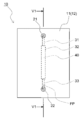
- FIG. 5 is a V1-V1 sectional view of FIG. 1. It is sectional drawing which shows typically the function of the easily deformable layer which the flow-path chip concerning one Embodiment of this invention has. It is a graph which shows the result of having analyzed using the channel chip concerning one embodiment of the present invention. It is a graph which shows the result of having analyzed using the channel chip for comparison. It is a flowchart of the manufacturing method of the flow-path chip
- FIG. 1 is a top view schematically showing a flow channel chip according to an embodiment of the present invention.
- 2 is a cross-sectional view taken along the line V1-V1 of FIG.
- the flow channel chip 10 is the same as the first plate 11 made of a translucent resin material, and the first plate 11 is the same quality.
- a second plate 12 joined to the first plate 11.
- the first plate 11 and the second plate 12 in the flow channel chip 10 according to the present embodiment are made of cycloolefin-containing polyolefin (polyolefin-based material) such as cycloolefin polymer (COC) and cycloolefin copolymer (COP).
- cycloolefin-containing polyolefin polyolefin-based material
- COC cycloolefin polymer
- COP cycloolefin copolymer
- resin materials that can constitute these plates include polyolefins other than cycloolefin-based polyolefins such as polyethylene (PE) and polypropylene (PE), acrylic resins such as polymethyl methacrylate (PMMA), polycarbonate (PC), silicone Resins are exemplified.
- a filler material such as silica may be dispersed in the first plate 11 and the second plate 12.
- n-alkane which is a kind of alkane, as an adhesive.
- the “adhesive” in this specification means a material that contributes to fixing (joining) the relative positions of two adherends (here, the first plate 11 and the second plate 12). To do. Therefore, a modified product in which at least one of the two adherends is modified by the adhesive may be formed, and the modified product may join the two adherends.
- an alkane in particular, a linear alkane (n-alkane) is used as a material for forming the modified product.
- the number of carbon atoms of the n-alkane is not limited, it may be preferable that the number of carbon atoms is about 5 to 9 from the viewpoint of high handleability and high bondability. Details of the bonding method using n-alkane will be described later.
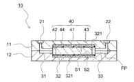
- the flow channel chip 10 has a flow channel FP formed by the first plate 11 and the second plate 12.
- the first flow path 31 and the second flow path 33 formed by the recesses formed in the first plate 11 and the recesses formed in the second plate 12, and the joint surface of the first plate 11, respectively.
- the flow path FP of the flow path chip 10 is configured by the accommodating portion 32 including the recess formed in the second plate 12.
- a column (processing body) 40 having a porous body 41 is disposed inside the accommodating portion 32. Specifically, the column 40 is sandwiched between the first plate 11 and the second plate 12.
- the porous body 41 that is the stationary phase of the column 40 is a structure mainly composed of silica having a monolith structure (silica monolith). Since the silica monolith is a sintered body of silica gel, it is harder than the material (resin-based material) constituting the first plate 11 and the second plate 12, but is brittle.
- the column 40 has pressure adjusting portions 42 and 43 having columnar outer shapes at both ends of the porous body 41 in the flow direction.
- the pressure adjusting units 42 and 43 have a function of adjusting the flow of a fluid (specific example is blood) flowing through the flow channel FP formed in the flow channel chip 10. That is, the pressure adjusting parts 42 and 43 have substantially the same pressure loss as the porous body 41.
- the pressure adjusting units 42 and 43 By providing the pressure adjusting units 42 and 43, the flow of the fluid to be pumped is adjusted, and the disturbance of the fluid passing through the column 40 is suppressed.
- the pressure adjusting units 42 and 43 have a filter function and a diffusion plate function, and in addition, have a material harder than the column 40.
- the column 40 has a coating layer 44 positioned so as to cover the porous body 41 and the pressure adjusting portions 42 and 43.
- a heat-shrinkable resin that shrinks by heating is used.
- the covering layer 44 has a tube shape, and the column 40 having a columnar outer shape is configured by housing the porous body 41 and the pressure adjusting portions 42 and 43 in the tube and heating them.
- the kind of heat-shrinkable resin is not limited. Examples thereof include tetrafluoroethylene / hexafluoropropylene copolymer (4,6 fluoride, FEP), polyetheretherketone (PEEK), and the like.
- the second surface S2 that is the surface facing the plate 11 is the surface of the easily deformable layer 321 (see FIG. 2).
- the “easily deformable layer” means the material used for the first plate 11 and the second plate 12 constituting the flow path FP of the flow path chip 10 (in the flow path chip 10 according to the present embodiment, cycloolefin-containing material). It is made of a softer material than (polyolefin). For this reason, when the column 40 which is a member including the porous body 41 is disposed in the accommodating portion 32, the porous body 41 may be preferentially deformed and an external force leading to breakage may be applied to the porous body 41. Can be reduced.
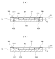
- FIG. 3 is a cross-sectional view schematically showing the function of the easily deformable layer included in the flow channel chip 10 according to the embodiment of the present invention.
- the bent portion BP of the column 40B is highlighted.
- the porous body 41 is a structure mainly composed of a sintered body of silica gel, it may be deformed during sintering.
- the porous body 41 included in the column 40B shown in FIG. 3 is bent rather than linear. In the case of having such an outer shape, even if it is covered with the coating layer 44, the shape of the column 40B as a whole is also deviated from the linear shape and has a bent portion BP.
- the bent portion BP is located on the side facing the second plate 12.
- the bent portion BP of the column 40B is made of the material constituting the second plate 12 (in the flow channel chip 10 according to the present embodiment, cycloolefin-containing material). (Polyolefin) directly. Since the shape of the concave portion forming the accommodating portion 32 in the second plate 12 is not a shape corresponding to the bent portion BP of the column 40B, the column 40B sandwiched between the first plate 11 and the second plate 12 in the accommodating portion 32 is The contact pressure of the bent part BP is relatively high. When the external force based on the contact pressure is large, the column 40B is damaged at the bent portion BP.
- the channel chip 10 cannot fulfill the purpose of analyzing the fluid using the column 40B. Therefore, if an attempt is made to obtain a flow path chip 10 that can be analyzed using the column 40B having the bent portion BP as shown in FIG. 3, the degree of clamping (bonding pressure) between the first plate and the second plate is increased. It is necessary to reduce it. When the bonding pressure is so low, the upper limit of the pressure that can be applied in the flow channel FP of the flow channel chip 10 is also low, causing problems such as a decrease in analysis speed.
- the first surface S1 and the second surface S2 of the housing portion 32 are surfaces of the easily deformable layer 321. Therefore, the bent portion BP of the column 40B contacts the easily deformable layer 321 on the second surface S2 side, and the easily deformable layer 321 is preferentially deformed at this portion, so that the porous portion BP located in the bent portion BP of the column 40B is located. The external force applied to the material body 41B is relieved. Moreover, since the easily deformable layer 321 is appropriately preferentially deformed at portions other than the bent portion BP, the uniformity of the pressure applied to the column 40B in the housing portion 32 can be enhanced.
- the increase in the uniformity of the pressure applied to the column 40B contributes to the improvement of the analysis accuracy using the column 40B.
- the housing portion 32 of the flow channel chip 10 and the porous body 41 can be further closely adhered to each other by the coating layer 44 covering the porous body 41B. For this reason, when a fluid flows into the flow path FP of the flow path chip 10, there is a low possibility that the fluid leaks from the joint surface between the first plate 11 and the second plate 12. The fluid can pass through the porous body 41 more stably.
- FIG. 4 shows the result of analysis using the channel chip 10 having the easily deformable layer 321
- FIG. 5 shows the analysis using the comparative channel chip having no easily deformable layer 321. Results are shown.
- FIG. 4 when the flow channel chip 10 having the easily deformable layer 321 is used, the analysis is appropriately performed even at a high pressure of about 10 MPa, and four peaks are detected.
- FIG. 5 in the case of the channel chip 10 from the low pressure stage of about 5 MPa when the comparative channel chip without the easily deformable layer 321 is used, the measurement is not performed.
- the number of peaks is four.
- the material constituting the easily deformable layer 321 is not limited.
- the easily deformable layer 321 is made of a modified product in which each of the first plate 11 and the second plate 12 is modified by a modifier. Is good. That is, the material constituting the first plate 11 and the second plate 12 (cycloolefin-containing polyolefin in the flow channel chip 10 according to this embodiment) is a part of the direct raw material member of the easily deformable layer 321. preferable. This will be described below.
- the problem that the easily deformable layer 321 is peeled off from the first plate 11 and the second plate 12 hardly occurs.
- the modifier for forming the easily deformable layer 321 is an adhesive used to join the first plate 11 and the second plate 12 described above, n ⁇ .
- the n-alkane modifies the material constituting the first plate 11 and the second plate 12 and improves the bondability thereof. Since the modified product of n-alkane has low mechanical properties, that is, is soft, it is suitable as a material constituting the easily deformable layer 321. Since the modifier, which is a material for forming the easily deformable layer 321, and the adhesive, which is a material for bonding the first plate 11 and the second plate 12, are common, It is possible to reduce the types of substances (constituent substances) used for manufacturing.
- composition analysis is performed using the channel chip 10
- a small number of substances constituting the channel chip 10 means that the number of substances that can be impurities in the analysis is small. Therefore, it is expected that a decrease in analysis accuracy is suppressed by using the flow channel chip 10 according to the present embodiment.
- the manufacturing method of the flow path chip 10 according to the present embodiment is not limited. If the manufacturing method described below is adopted, the flow channel chip 10 can be efficiently manufactured.
- FIG. 6 is a flowchart of the manufacturing method of the flow channel chip 10 according to an embodiment of the present invention.
- FIG. 7 is a cross-sectional view schematically showing a method for manufacturing the flow path chip 10 according to an embodiment of the present invention (stage where a plate is prepared), and FIG. 7A is a cross-sectional view of the first plate.
- FIG. 7B is a sectional view of the second plate.
- FIG. 8 is a cross-sectional view schematically showing a manufacturing method of the flow channel chip 10 according to an embodiment of the present invention (the stage where the coating operation related to the first coating process and the second coating process is completed).
- 8 (a) is a sectional view of the first plate
- FIG. 8 (b) is a sectional view of the second plate.
- FIG. 9 is a cross-sectional view schematically showing a method for manufacturing the flow channel chip 10 according to an embodiment of the present invention (stage where the first application step and the second application step are completed), and FIG. Is a cross-sectional view of the first plate, and FIG. 9B is a cross-sectional view of the second plate.
- FIG. 10 is a cross-sectional view schematically showing a method for manufacturing the flow path chip 10 according to an embodiment of the present invention (the stage where the loading process is completed).
- FIG. 11 is a cross-sectional view schematically showing a method for manufacturing the flow path chip 10 according to an embodiment of the present invention (the stage where the joining process is completed).
- the column 40B deformed at the time of sintering is used, but the present invention is not limited to this, and the column 40 may be used.
- the first plate 11 and the second plate 12 to be joined are prepared (S101), and the n-alkane is added thereto. Is applied (S102), the column 40B is loaded (S103), and the first plate 11 and the second plate 12 are joined (S104), whereby the flow channel chip 10 is manufactured.
- the first plate 11 includes a through-hole 121 corresponding to the inflow portion 21, a through-hole 122 corresponding to the outflow portion 22, a recess 131 for forming the first flow path 31, It has the recessed part 133 for forming the 2nd flow path 33, and the 1st recessed part 132 which is a recessed part for forming the accommodating part 32.
- FIG. 7A the first plate 11 includes a through-hole 121 corresponding to the inflow portion 21, a through-hole 122 corresponding to the outflow portion 22, a recess 131 for forming the first flow path 31, It has the recessed part 133 for forming the 2nd flow path 33, and the 1st recessed part 132 which is a recessed part for forming the accommodating part 32.
- the second plate 12 forms a recess 231 for forming the first flow path 31, a recess 233 for forming the second flow path 33, and a housing part 32.
- a second recess 232 which is a recess for the purpose.
- the method for preparing the first plate 11 and the second plate 12 is not limited.
- the first plate 11 and the second plate 12 may be obtained by a molding process such as injection molding, or the first plate 11 and the second plate 12 may be obtained by subjecting a plate-like member to machining such as grooving or drilling. It may be formed. Moreover, you may combine these shaping
- the surfaces to be joined surfaces (hereinafter referred to as the planned joining surface S11 and the planned joining surface S12) are shown. Arrange them so that each is on top.
- the surface S21 of the 1st recessed part 132 and the surface S22 of the 2nd recessed part 232 may also be on the upper side. It is configured.
- the adhesive AD can be applied in an arbitrary amount in an arbitrary place by using an ink jet device or a dispenser.
- the amount of the adhesive AD applied to the surface S21 of the first recess 132 and the surface S22 of the second recess 232 is the same as the adhesive applied to the surfaces to be joined S11 and S12. More than the amount of AD. As a result, as shown in FIG.
- the thickness t1 of the adhesive AD applied to the surface S21 of the first recess 132 is greater than the thickness t11 of the adhesive AD applied to the planned bonding surface S11. Also thick. As shown in FIG. 8B, the thickness t1 of the adhesive AD applied to the surface S22 of the second recess 232 is also thicker than the thickness t11 of the adhesive AD applied to the planned bonding surface S12.
- the thickness t2 of the modified layer (the easily deformable layer 321) formed in the first plate 11 and the second plate 12 is to be bonded. It is thicker than the thickness t12 of the modified layer ML formed on the surfaces S11 and S12 (S102).
- the easily deformable layer 321 made of the modified layer formed on the first plate 11 and the second plate 12 can have appropriate mechanical properties (softness), and the column 40B can be damaged in the joining process. Can be reduced.
- the degree of formation of the easily deformable layer 321 is adjusted by adjusting the amount of the adhesive AD applied per unit area on at least a part of the surface S21 of the first recess 132 and the surface S22 of the second recess 232. Is preferably controlled. That is, since the easily deformable layer 321 is formed by modifying the material constituting the first plate 11 or the material constituting the second plate 12 with the adhesive AD, the degree of application of the adhesive AD It is possible to control the degree of formation (thickness (depth), physical properties (softness), etc.) of the easily deformable layer 321 by adjusting.
- the degree of formation of the easily deformable layer 321 is changed according to the shape of the member to be accommodated (column 40B) including the porous body 41 sandwiched between the first plate 11 and the second plate 12, and the porous body 41 is changed. It is easy to control fine manufacturing conditions such as reducing the possibility of damage in a more stable manner. Therefore, it is possible to manufacture a high quality flow path chip 10.
- the column 40B is disposed so as to be in contact with the second surface S2 of the second recess 232 of the second plate 12 as shown in FIG. 10 (S103). At this stage, the deformation of the easily deformable layer 321 is limited.
- the first plate 11 on which the easily deformable layer 321 is formed is brought into contact with the second plate 12 so that the bonding planned surfaces S11 and S12 face each other.
- the first plate 11 and the second plate 12 are joined on the joining surfaces S11 and S12 (S104).
- the contact conditions are set as appropriate.
- the first plate 11 and the second plate 12 are brought into contact with each other at a pressing force of 0.5 MPa to 5 MPa for 5 minutes to 30 minutes to join them. .
- the flow channel chip 10 is obtained by forming the flow channel FP including the accommodating portion 32 that accommodates the column 40B in a state where at least a part of the easily deformable layer 321 is deformed by the column 40B.
- the material for joining the first plate 11 and the second plate 12 and the material for forming the easily deformable layer 321 are common (adhesive AD made of n-alkane). Therefore, an increase in the number of material types necessary for manufacturing is suppressed, and the flow channel chip 10 having the easily deformable layer 321 can be efficiently manufactured.
- the first application step of applying the adhesive AD to the bonding scheduled surfaces S11 and S12, and the first application of the adhesive AD to the surface S21 of the first recess 132 and the surface S22 of the second recess 232 are performed.
- the two coating process is performed as one process. Since the material for joining the first plate 11 and the second plate 12 and the material for forming the easily deformable layer 321 are common (adhesive agent AD), in the first plate 11, the joining scheduled surface S11.
- the operation of applying the adhesive AD to the surface and the operation of applying the adhesive AD to the surface S21 of the first recess 132 can be performed simultaneously or continuously.
- the operation of applying the adhesive AD to the planned bonding surface S12 and the operation of applying the adhesive AD to the surface S22 of the second recess 232 are performed simultaneously or continuously. Can do.
- the 1st application process and the 2nd application process about the 1st plate 11 or the 2nd plate 12 can be completed by one application work, workability of the whole application process can be improved. Therefore, the channel chip 10 can be easily manufactured.
- the material constituting the first plate 11 and the second plate 12 may not be a resin material and may not have translucency.
- the material constituting the first plate 11 and the second plate 12 may not be a resin material and may not have translucency.
- at least one of the first plate 11 and the second plate 12 has translucency, at least a part of the second flow path 33 through which the fluid after passing through the column 40 flows is translucent. Will have. Therefore, it is possible to optically measure the separated state of the fluid in this portion.
- the first plate 11 and the second plate 12 are bonded using the adhesive AD made of n-alkane, but the present invention is not limited to this.
- the first plate 11 and the second plate 12 may be joined by fusion, or a layer made of another adhesive may be provided between these plates.
- the entire surface of the first surface S ⁇ b> 1 and the entire surface of the second surface S ⁇ b> 2 are configured by the surface of the easily deformable layer 321, but the present invention is not limited to this.
- the easily deformable layer 321 may not be provided in the portion where the pressure adjusting portions 42 and 43 are located, and the pressure adjusting portions 42 and 43 may be partially deformed to improve the adhesion of the column 40 to the housing portion 32. .
Abstract
Provided is a flow channel chip 10 in which two members are appropriately joined to each other and the possibility of a porous body disposed inside a processing tank formed by the two members becoming damaged is reduced, the flow channel chip being provided with a first plate 11, a second plate 12 joined to the first plate 11, and a porous body 41 which is disposed between the first plate 11 and the second plate 12, wherein the flow channel chip has a flow channel formed by the first plate 11 and the second plate 12. In this flow channel chip 10, the flow channel has an accommodation part 32 for accommodating the porous body 41, and the accommodation part 32 is defined by a first surface S1 and a second surface S2, the first surface being composed of a portion of the surface of the first plate 11 and the second surface being composed of a portion of the surface of the second plate 12, wherein at least a portion of the first surface S1 and at least a portion of the second surface S2 are surfaces of an easily-deformable layer 321, and the porous body 41 is sandwiched in a state in which at least a portion of the easily-deformable layer 321 is deformed.
Description
本発明は、流路チップ及び流路チップの製造方法に関する。
The present invention relates to a channel chip and a method for manufacturing the channel chip.
少量の流体を混合し又は反応させあるいは分離する装置としてマイクロ流路装置が使用されている。
A micro-channel device is used as a device for mixing, reacting or separating a small amount of fluid.
特許文献1には、処理槽と、前記処理槽に至る入力通路と、前記処理槽から延びる出力通路とが内部に形成された板状の本体部、及び前記処理槽の内部に配置された処理体とが設けられたマイクロ流路装置において、前記処理体は、多孔質体と前記多孔質体を囲む合成樹脂製の被覆層とを有し、前記被覆層が前記処理槽の内面に密着しており、前記被覆層に、前記入力通路と前記多孔質体とを連通する浸入口と、前記多孔質体と前記出力通路とを連通する浸出口が形成されているマイクロ流路装置が記載されている。
Patent Document 1 discloses a processing tank, a plate-shaped main body formed therein with an input passage leading to the processing tank, and an output passage extending from the processing tank, and a processing disposed in the processing tank. In the microchannel device provided with a body, the treatment body has a porous body and a synthetic resin coating layer surrounding the porous body, and the coating layer is in close contact with the inner surface of the treatment tank. And a microchannel device in which an inlet that communicates the input passage and the porous body and an inlet that communicates the porous body and the output passage are formed in the coating layer. ing.
特許文献1に記載されるマイクロ流路装置(流路チップ)では、処理溶液が多孔質体中を確実に通過するように、第1の本体プレートと第2の本体プレートとの接合や処理体の被覆層と処理槽の内面との密着が確実に行われていることが必要となっている。
In the microchannel device (channel chip) described in Patent Document 1, the first body plate and the second body plate are bonded to each other and the processing body so that the processing solution can surely pass through the porous body. It is necessary that the coating layer and the inner surface of the treatment tank be securely adhered to each other.
しかしながら、接合及び密着を確実にするため、加熱し且つ加圧する工程において、強い加圧力で行うと、多孔質体が破壊するおそれがあった。一方、弱い加圧力で行うと、接合及び密着が適切に行われず、液漏れが生じるおそれがあった。
However, in order to ensure bonding and adhesion, the porous body may be destroyed if it is applied with a strong pressure in the heating and pressurizing step. On the other hand, when it was performed with a weak pressure, joining and adhesion were not performed properly, and there was a risk of liquid leakage.
本発明は、2つの部材で多孔質体を含む部材を挟持する構造を有する流路チップにおいて、2つの部材を適切に接合しつつ、これらの部材によって形成される処理槽(収容部)内に配置される多孔質体が破損する可能性が低減された流路チップ、及びかかる流路チップの製造方法を提供することを目的とする。
The present invention relates to a flow path chip having a structure in which a member including a porous body is sandwiched between two members, while appropriately joining the two members, in a treatment tank (housing portion) formed by these members. It is an object of the present invention to provide a flow channel chip in which the possibility of breakage of a porous body to be disposed is reduced, and a method for manufacturing the flow channel chip.
上記の課題を解決するために提供される本発明は、その一態様において、第1プレートと、前記第1プレートに接合する第2プレートと、前記第1プレートと前記第2プレートとの間に配設される多孔質体と、を備え、前記第1プレートと前記第2プレートとによって形成される流路を有した流路チップであって、前記流路は、前記多孔質体を収容する収容部を有し、前記収容部は、前記第1プレートの面の一部からなる第1表面及び第2プレートの面の一部からなる第2表面により画成され、前記第1表面の少なくとも一部及び前記第2表面の少なくとも一部は、易変形層の面であって、前記多孔質体は、前記易変形層の少なくとも一部を変形させた状態で挟持されることを特徴とする流路チップである。
In one aspect, the present invention provided to solve the above problems includes a first plate, a second plate joined to the first plate, and between the first plate and the second plate. A flow path chip having a flow path formed by the first plate and the second plate, wherein the flow path accommodates the porous body. A housing part, the housing part being defined by a first surface comprising a part of the surface of the first plate and a second surface comprising a part of the surface of the second plate; A part and at least a part of the second surface are surfaces of the easily deformable layer, and the porous body is sandwiched with at least a part of the easily deformable layer deformed. It is a channel chip.
多孔質体は脆性材料からなるため、かかる構成の流路チップでは、第1プレートと第2プレートとによって挟み込まれたときに、多孔質体が収容部内で破損する場合があった。しかしながら、多孔質体を収容する収容部を画成している第1表面の少なくとも一部及び第2表面の少なくとも一部が易変形層からなることによって、多孔質体が第1プレートと第2プレートとによって挟み込まれたときに、多孔質体の外形に応じて易変形層が変形することができる。このため、多孔質体の破損が回避される。
Since the porous body is made of a brittle material, in the flow path chip having such a configuration, the porous body may be damaged in the accommodating portion when sandwiched between the first plate and the second plate. However, at least a part of the first surface and at least a part of the second surface that define the accommodating portion that accommodates the porous body are made of the easily deformable layer, so that the porous body is in contact with the first plate and the second plate. When sandwiched between the plates, the easily deformable layer can be deformed according to the outer shape of the porous body. For this reason, damage to the porous body is avoided.
上記の流路チップにおいて、前記多孔質体と前記易変形層との間に前記多孔質体を覆う被覆層を備えてもよい。
In the above-described flow channel chip, a coating layer that covers the porous body may be provided between the porous body and the easily deformable layer.
多孔質体が第1プレートと第2プレートとによって挟み込まれたときに、この被覆層によっても多孔質体への押し圧が緩和される。このことにより、多孔質体が破損する可能性がより安定的に低下する。
When the porous body is sandwiched between the first plate and the second plate, the pressure applied to the porous body is also reduced by this coating layer. By this, possibility that a porous body will be damaged will fall more stably.
上記の流路チップにおいて、前記易変形層は、前記第1プレート及び前記第2プレートの少なくとも一方が改質剤によって改質された改質物から構成されていてもよい。
In the flow channel chip, the easily deformable layer may be formed of a modified product in which at least one of the first plate and the second plate is modified by a modifying agent.
第1プレート及び/又は第2プレートを構成する材料が易変形層の直接的な原料部材の一部であるため、易変形層が剥離する不具合が生じにくい。したがって、流路内に液体を流した際に、隔離部分からの液漏れが生じにくくなって、液体が多孔質体内をより安定的に通過することができる。
Since the material constituting the first plate and / or the second plate is a part of the direct raw material member of the easily deformable layer, it is difficult for the easily deformable layer to peel off. Therefore, when the liquid is caused to flow through the flow path, liquid leakage from the isolation portion hardly occurs, and the liquid can pass through the porous body more stably.
上記の流路チップにおいて、前記第1プレートと前記第2プレートとは接着剤によって接合された部分を含み、前記接着剤は前記改質剤から構成されていてもよい。
In the above-described flow path chip, the first plate and the second plate may include a portion joined by an adhesive, and the adhesive may be composed of the modifier.
本明細書において「接着剤」とは、2つの被着体の相対位置を固定する(接合する)ことに資する材料を意味する。接着剤は接着剤層を形成して2つの被着体の間に位置して2つの被着体を接合してもよいし、接着剤によって2つの被着体の少なくとも一方が改質された改質物が形成され、この改質物が2つの被着体を接合してもよい。この改質物の一例として、被着体を構成する材料が軟質化したものが挙げられる。この場合には被着体が軟質化することによって、相手の被着体に対するアンカー効果が増大し、その結果、2つの被着体の相対位置が固定されやすくなる。
In this specification, “adhesive” means a material that contributes to fixing (joining) the relative positions of two adherends. The adhesive may form an adhesive layer and be positioned between the two adherends to join the two adherends, or at least one of the two adherends is modified by the adhesive. A modified product may be formed, and the modified product may join two adherends. As an example of this modified product, a material in which the material constituting the adherend is softened can be given. In this case, since the adherend is softened, the anchor effect on the other adherend is increased, and as a result, the relative positions of the two adherends are easily fixed.
易変形層を形成するための材料である改質剤と、第1プレートと第2プレートとを結合させるための材料である接着剤とが共通であることにより、流路チップを製造するために用いられる物質(構成物質)の種類を少なくすることが可能である。流路チップを用いて組成分析を行う場合には、流路チップを構成する物質の種類が少ないことは、分析における不純物となりうる物質数が少ないことを意味する。したがって、分析精度の低下が抑制されることが期待される。
In order to manufacture the flow channel chip, the modifier, which is a material for forming the easily deformable layer, and the adhesive, which is a material for bonding the first plate and the second plate, are common. It is possible to reduce the types of substances (constituent substances) used. When composition analysis is performed using a channel chip, the fact that the number of substances constituting the channel chip is small means that the number of substances that can be impurities in the analysis is small. Therefore, it is expected that a decrease in analysis accuracy is suppressed.
上記の流路チップにおいて、前記第1プレート及び前記第2プレートはポリオレフィン系材料からなり、前記接着剤はアルカンを含んでいてもよい。
In the flow channel chip, the first plate and the second plate may be made of a polyolefin-based material, and the adhesive may include alkane.
ポリオレフィン系材料からなる部材はアルカンによって接合することが可能であり、アルカンによってポリオレフィン系材料を軟質化させること(改質すること)が可能である。したがって、第1プレートと第2プレートとがポリオレフィン系材料からなり、接合材料がアルカンを含むことにより、第1プレートと第2プレートとの接合がより確実なものとなり、しかも有効な易変形層が形成されやすい。
A member made of a polyolefin-based material can be joined by an alkane, and the polyolefin-based material can be softened (modified) by the alkane. Therefore, the first plate and the second plate are made of a polyolefin-based material, and the joining material contains alkane, so that the joining of the first plate and the second plate is more reliable, and an effective easily deformable layer is provided. Easy to form.
本発明は、別の一態様として、第1凹部を有する第1プレートと、第2凹部を有し前記第1プレートに接合される第2プレートと、前記第1プレートと該第2プレートとの間に配設される多孔質体と、を備え、前記第1凹部と前記第2凹部とによって形成され前記多孔質体を収容する収容部を含む流路が設けられた流路チップの製造方法を提供する。かかる製造方法は、前記第1プレートの前記第2プレートへの接合面となるべき面及び前記第2プレートの前記第1プレートへの接合面となるべき面の少なくとも一方に、前記第1プレートと前記第2プレートとを接合するための接着剤を塗布する第1塗布工程と、前記第1凹部の面の少なくとも一部及び前記第2凹部の面の少なくとも一部に前記接着剤を塗布して、前記第1凹部の面及び前記第2凹部の面の少なくとも一部を易変形層の面とする第2塗布工程と、前記第1凹部の面及び前記第2凹部の面の少なくとも一方に接するように、前記多孔質体を含む被収容部材を配設する装填工程と、前記第1プレートの接合面となるべき面と前記第2プレートの接合面となるべき面とを対向させて接触させることにより、前記第1プレートと前記第2プレートとを接合するとともに、前記被収容部材により前記易変形層の少なくとも一部が変形した状態で前記被収容部材を収容する前記収容部を含む前記流路を形成して、前記流路チップを得る接合工程と、を備えることを特徴とする。
According to another aspect of the present invention, a first plate having a first recess, a second plate having a second recess and joined to the first plate, the first plate, and the second plate A flow path chip provided with a flow path including an accommodating portion that is formed by the first recess and the second recess and accommodates the porous body. I will provide a. The manufacturing method includes the first plate on at least one of a surface to be a bonding surface of the first plate to the second plate and a surface to be a bonding surface of the second plate to the first plate. A first application step of applying an adhesive for joining the second plate; and applying the adhesive to at least a part of the surface of the first recess and at least a part of the surface of the second recess. A second coating step in which at least a part of the surface of the first recess and the surface of the second recess is a surface of the easily deformable layer; and at least one of the surface of the first recess and the surface of the second recess As described above, the loading step of disposing the member to be contained including the porous body, and the surface to be the bonding surface of the first plate and the surface to be the bonding surface of the second plate are brought into contact with each other. The first plate and the front The flow path including the accommodating portion that accommodates the accommodated member in a state where at least a part of the easily deformable layer is deformed by the accommodated member is formed while joining the second plate, And a bonding step for obtaining a chip.
かかる製造方法によれば、第1プレートと第2プレートとを接合するための材料と、易変形層を形成するための材料とが共通であるため、製造に必要な材料種類が多くなることが抑制され、易変形層を有する流路チップを効率的に製造することができる。
According to such a manufacturing method, since the material for joining the first plate and the second plate and the material for forming the easily deformable layer are common, the types of materials necessary for manufacturing may increase. The flow path chip that is suppressed and has the easily deformable layer can be efficiently manufactured.
上記の製造方法において、前記第1塗布工程と前記第2塗布工程とは一つの工程として行われてもよい。このように製造することにより、第1プレートと第2プレートとを接合するための材料と、易変形層を形成するための材料とが共通であるため、第1プレートの第2プレートへの接合面となるべき面への接着剤を塗布する作業と、第1凹部の面に接着剤を塗布する作業とを、同時に、又は連続的に行うことができる。同様に、第2プレートの第1プレートへの接合面となるべき面への接着剤を塗布する作業と、第2凹部の面に接着剤を塗布する作業とを、同時に、又は連続的に行うことができる。このように、第1プレート又は第2プレートに関する第1塗布工程及び第2塗布工程を一回の塗布作業により完了させることができるため、塗布工程全体の作業性を高めることができる。したがって、流路チップを容易に製造することができる。
In the above manufacturing method, the first application step and the second application step may be performed as one step. By manufacturing in this way, the material for joining the first plate and the second plate and the material for forming the easily deformable layer are common, so the first plate is joined to the second plate. The operation | work which applies the adhesive agent to the surface which should become a surface, and the operation | work which apply | coats an adhesive agent to the surface of a 1st recessed part can be performed simultaneously or continuously. Similarly, the operation | work which applies the adhesive agent to the surface which should become a joint surface to the 1st plate of a 2nd plate and the operation | work which apply | coats an adhesive agent to the surface of a 2nd recessed part are performed simultaneously or continuously. be able to. Thus, since the 1st application process and the 2nd application process about the 1st plate or the 2nd plate can be completed by one application work, workability of the whole application process can be improved. Therefore, the channel chip can be easily manufactured.
上記の製造方法において、前記第1凹部の面及び前記第2凹部の面の少なくとも一部について、塗布される前記接着剤の単位面積当たりの量を調整して、前記易変形層の形成の程度を制御してもよい。易変形層は第1プレートを構成する材料や第2プレートを構成する材料が接着剤により改質されることにより形成されるものであるから、接着剤の塗布の程度を調整することにより易変形層の形成の程度(厚さ(深さ)や物性(軟らかさ)など)を制御することができる。したがって、第1プレート及び第2プレートに挟持される多孔質体を含む部材の形状に応じて易変形層の形成の程度を変化させて、多孔質体の破損の可能性をより安定的に低下させる、といった細やかな製造条件の制御が容易となる。それゆえ、品質の高い流路チップを製造することが可能である。
In the manufacturing method described above, the degree of formation of the easily deformable layer is adjusted by adjusting the amount of the adhesive applied per unit area for at least a part of the surface of the first recess and the surface of the second recess. May be controlled. Since the easily deformable layer is formed by modifying the material constituting the first plate or the material constituting the second plate with an adhesive, it can be easily deformed by adjusting the degree of application of the adhesive. The degree of layer formation (thickness (depth), physical properties (softness), etc.) can be controlled. Therefore, the degree of formation of the easily deformable layer is changed according to the shape of the member including the porous body sandwiched between the first plate and the second plate, and the possibility of damage to the porous body is more stably reduced. This makes it easy to control detailed manufacturing conditions. Therefore, it is possible to manufacture a high quality channel chip.
本発明によれば、2つの部材で多孔質体を含む部材を挟持する構造を有する流路チップであって、2つの部材を適切に接合しつつ、これらの部材によって形成される収容部内に配置される多孔質体が破損する可能性が低減された流路チップ、及びかかる流路チップの製造方法が提供される。
According to the present invention, a flow path chip having a structure in which a member including a porous body is sandwiched between two members, and the two members are appropriately joined and disposed in a housing portion formed by these members. Provided are a flow channel chip in which the possibility of damage to a porous body to be damaged is reduced, and a method for manufacturing the flow channel chip.
以下、本発明の実施の形態について図面を参照しつつ説明する。なお、各図面中、同様の構成要素には同一の符号を付して詳細な説明は適宜省略する。
Hereinafter, embodiments of the present invention will be described with reference to the drawings. In addition, in each drawing, the same code | symbol is attached | subjected to the same component and detailed description is abbreviate | omitted suitably.
図1は、本発明の一実施形態に係る流路チップを模式的に示す上面図である。図2は、図1のV1-V1断面図である。
FIG. 1 is a top view schematically showing a flow channel chip according to an embodiment of the present invention. 2 is a cross-sectional view taken along the line V1-V1 of FIG.
図1及び図2に示されるように、本発明の一実施形態に係る流路チップ10は、透光性の樹脂系材料からなる第1プレート11と、第1プレート11と同質であって第1プレート11に接合する第2プレート12と、を備える。本実施形態に係る流路チップ10における第1プレート11及び第2プレート12は、シクロオレフィンポリマー(COC)、シクロオレフィンコポリマー(COP)等シクロオレフィン含有ポリオレフィン(ポリオレフィン系材料)から構成されている。これらのプレートの構成材料となりうる他の樹脂材料として、ポリエチレン(PE)、ポリプロピレン(PE)等のシクロオレフィン系ポリオレフィン以外のポリオレフィン、ポリメチルメタクリレート(PMMA)等アクリル系樹脂、ポリカーボネート(PC)、シリコーン樹脂などが例示される。第1プレート11及び第2プレート12には、シリカなどのフィラー材が分散していてもよい。
As shown in FIG. 1 and FIG. 2, the flow channel chip 10 according to an embodiment of the present invention is the same as the first plate 11 made of a translucent resin material, and the first plate 11 is the same quality. A second plate 12 joined to the first plate 11. The first plate 11 and the second plate 12 in the flow channel chip 10 according to the present embodiment are made of cycloolefin-containing polyolefin (polyolefin-based material) such as cycloolefin polymer (COC) and cycloolefin copolymer (COP). Other resin materials that can constitute these plates include polyolefins other than cycloolefin-based polyolefins such as polyethylene (PE) and polypropylene (PE), acrylic resins such as polymethyl methacrylate (PMMA), polycarbonate (PC), silicone Resins are exemplified. A filler material such as silica may be dispersed in the first plate 11 and the second plate 12.
第1プレート11と第2プレート12とは、アルカンの一種であるn-アルカンを接着剤として接合されている。前述のように、本明細書において「接着剤」とは、2つの被着体(ここでは第1プレート11及び第2プレート12)の相対位置を固定する(接合する)ことに資する材料を意味する。したがって、接着剤によって2つの被着体の少なくとも一方が改質された改質物が形成され、この改質物が2つの被着体を接合してもよい。本実施形態に係る流路チップ10では、この改質物を形成するための材料として、アルカン、特に、直鎖状のアルカン(n-アルカン)が用いられている。n-アルカンの炭素数は限定されないが炭素数が5から9程度であることが、取扱い性の高さ及び接合性の高さの観点から好ましい場合がある。n-アルカンを用いた接合方法の詳細については後述する。
The first plate 11 and the second plate 12 are joined using n-alkane, which is a kind of alkane, as an adhesive. As described above, the “adhesive” in this specification means a material that contributes to fixing (joining) the relative positions of two adherends (here, the first plate 11 and the second plate 12). To do. Therefore, a modified product in which at least one of the two adherends is modified by the adhesive may be formed, and the modified product may join the two adherends. In the flow channel chip 10 according to the present embodiment, an alkane, in particular, a linear alkane (n-alkane) is used as a material for forming the modified product. Although the number of carbon atoms of the n-alkane is not limited, it may be preferable that the number of carbon atoms is about 5 to 9 from the viewpoint of high handleability and high bondability. Details of the bonding method using n-alkane will be described later.
流路チップ10は、図1及び図2に示されるように、第1プレート11と前記第2プレート12とによって形成される流路FPを有する。具体的には、それぞれ第1プレート11に形成された凹部と第2プレート12に形成された凹部とによって形成される第1流路31及び第2流路33、第1プレート11の接合面とは反対側の面に形成された開口から第1流路31の一方の端部に至る流入部21、第1プレート11の接合面とは反対側の面に形成された開口から第2流路33の一方の端部に至る流出部22、及び第1流路31の他方の端部と第2流路33の他方の端部との間に位置し、第1プレート11に形成された凹部と第2プレート12に形成された凹部とからなる収容部32によって、流路チップ10の流路FPは構成されている。
As shown in FIGS. 1 and 2, the flow channel chip 10 has a flow channel FP formed by the first plate 11 and the second plate 12. Specifically, the first flow path 31 and the second flow path 33 formed by the recesses formed in the first plate 11 and the recesses formed in the second plate 12, and the joint surface of the first plate 11, respectively. Is an inflow portion 21 extending from an opening formed on the opposite surface to one end of the first flow channel 31, and an opening formed on the surface opposite to the bonding surface of the first plate 11 to the second flow channel. A recess formed in the first plate 11, located between the outflow part 22 reaching one end of 33 and the other end of the first flow path 31 and the other end of the second flow path 33. The flow path FP of the flow path chip 10 is configured by the accommodating portion 32 including the recess formed in the second plate 12.
収容部32の内部には、多孔質体41を有するカラム(処理体)40が配設されている。具体的には、第1プレート11と第2プレート12とによって、カラム40は挟持されている。
A column (processing body) 40 having a porous body 41 is disposed inside the accommodating portion 32. Specifically, the column 40 is sandwiched between the first plate 11 and the second plate 12.
本実施形態に係る流路チップ10において、カラム40の固定相である多孔質体41はモノリス構造を有するシリカ(シリカモノリス)を主体とする構造体である。シリカモノリスはシリカゲルの焼結体であるため、第1プレート11及び第2プレート12を構成する材料(樹脂系材料)よりも硬質であるが、脆い。
In the flow channel chip 10 according to the present embodiment, the porous body 41 that is the stationary phase of the column 40 is a structure mainly composed of silica having a monolith structure (silica monolith). Since the silica monolith is a sintered body of silica gel, it is harder than the material (resin-based material) constituting the first plate 11 and the second plate 12, but is brittle.
カラム40は、多孔質体41における流れ方向の両端に、柱状の外形を有する圧力調整部42,43を有する。圧力調整部42,43は、流路チップ10に形成された流路FPを流れる流動物(具体例として血液が挙げられる。)の流れを調整する機能を有する。すなわち、圧力調整部42,43は、多孔質体41とほぼ同じ圧力損失を持つ。圧力調整部42,43を設けることで、圧送される流動物の流れが調整され、カラム40を通過する流動物の乱れが抑制される。また、圧力調整部42,43は、フィルター機能と、拡散板の機能とを備え、それに加えてカラム40よりも硬い材質を有している。
The column 40 has pressure adjusting portions 42 and 43 having columnar outer shapes at both ends of the porous body 41 in the flow direction. The pressure adjusting units 42 and 43 have a function of adjusting the flow of a fluid (specific example is blood) flowing through the flow channel FP formed in the flow channel chip 10. That is, the pressure adjusting parts 42 and 43 have substantially the same pressure loss as the porous body 41. By providing the pressure adjusting units 42 and 43, the flow of the fluid to be pumped is adjusted, and the disturbance of the fluid passing through the column 40 is suppressed. In addition, the pressure adjusting units 42 and 43 have a filter function and a diffusion plate function, and in addition, have a material harder than the column 40.
カラム40は、多孔質体41及び圧力調整部42,43を覆うように位置する被覆層44を有する。被覆層44には、例えば加熱によって収縮する熱収縮性樹脂が用いられる。被覆層44はチューブ状になっており、このチューブ内に多孔質体41及び圧力調整部42,43を収納して加熱することで柱状の外形を有するカラム40が構成される。熱収縮性樹脂の種類は限定されない。テトラフルオロエチレン・ヘキサフルオロプロピレン共重合体(4,6フッ化体、FEP)、ポリエーテルエーテルケトン(PEEK)などが例示される。使用時においては、流入部21から第1流路31を経て収容部32内に流動物が供給されると、カラム40内に数MPa又はそれ以上の圧力が加えられる。この場合においても、多孔質体41と被覆層44との間に隙間が生じにくくする観点から、熱収縮性樹脂としてPEEKを用いることが好ましい。熱収縮性樹脂としてPEEKを用いることにより、流動物の供給圧力が10MPaより高くなっても適切に分析を行うことができる場合がある。
The column 40 has a coating layer 44 positioned so as to cover the porous body 41 and the pressure adjusting portions 42 and 43. For the coating layer 44, for example, a heat-shrinkable resin that shrinks by heating is used. The covering layer 44 has a tube shape, and the column 40 having a columnar outer shape is configured by housing the porous body 41 and the pressure adjusting portions 42 and 43 in the tube and heating them. The kind of heat-shrinkable resin is not limited. Examples thereof include tetrafluoroethylene / hexafluoropropylene copolymer (4,6 fluoride, FEP), polyetheretherketone (PEEK), and the like. In use, when a fluid is supplied from the inflow portion 21 through the first flow path 31 into the accommodating portion 32, a pressure of several MPa or more is applied to the column 40. Even in this case, it is preferable to use PEEK as the heat-shrinkable resin from the viewpoint of making it difficult for a gap to be formed between the porous body 41 and the coating layer 44. By using PEEK as the heat-shrinkable resin, it may be possible to appropriately analyze even when the supply pressure of the fluid is higher than 10 MPa.
収容部32を構成する第1プレート11の凹部の面のうち第2プレート12に対向する面である第1表面S1、及び収容部32を構成する第2プレート12の凹部の面のうち第1プレート11に対向する面である第2表面S2は、易変形層321の面である(図2を参照)。本明細書において「易変形層」とは、流路チップ10の流路FPを構成する第1プレート11及び第2プレート12に用いた材料(本実施形態に係る流路チップ10ではシクロオレフィン含有ポリオレフィン)に比べて軟質な材料から構成される。このため、多孔質体41を含む部材であるカラム40が収容部32に配設されたときに、優先的に変形して、多孔質体41に対して破損に至る外力が付与される可能性を低減させることができる。
The first surface S1 which is the surface facing the second plate 12 among the concave surfaces of the first plate 11 constituting the accommodating portion 32 and the first of the concave surfaces of the second plate 12 constituting the accommodating portion 32. The second surface S2 that is the surface facing the plate 11 is the surface of the easily deformable layer 321 (see FIG. 2). In this specification, the “easily deformable layer” means the material used for the first plate 11 and the second plate 12 constituting the flow path FP of the flow path chip 10 (in the flow path chip 10 according to the present embodiment, cycloolefin-containing material). It is made of a softer material than (polyolefin). For this reason, when the column 40 which is a member including the porous body 41 is disposed in the accommodating portion 32, the porous body 41 may be preferentially deformed and an external force leading to breakage may be applied to the porous body 41. Can be reduced.
図3は、本発明の一実施形態に係る流路チップ10が有する易変形層の機能を模式的に示す断面図である。なお、説明を分かり易くするため、カラム40Bの屈曲部BPを強調して記している。前述のように、多孔質体41はシリカゲルの焼結体を主体とする構造体であるため、焼結の際に変形する場合がある。図3に示されるカラム40Bが有する多孔質体41は、直線形状ではなく屈曲している。このような外形を有している場合には、被覆層44で覆っても、カラム40B全体としての形状は、やはり直線形状から外れて屈曲部BPを有する形状となる。図3に示されるカラム40Bは、第2プレート12に対向する側に屈曲部BPが位置する。
FIG. 3 is a cross-sectional view schematically showing the function of the easily deformable layer included in the flow channel chip 10 according to the embodiment of the present invention. For easy understanding, the bent portion BP of the column 40B is highlighted. As described above, since the porous body 41 is a structure mainly composed of a sintered body of silica gel, it may be deformed during sintering. The porous body 41 included in the column 40B shown in FIG. 3 is bent rather than linear. In the case of having such an outer shape, even if it is covered with the coating layer 44, the shape of the column 40B as a whole is also deviated from the linear shape and has a bent portion BP. In the column 40 </ b> B shown in FIG. 3, the bent portion BP is located on the side facing the second plate 12.
流路チップ10の収容部32が易変形層321を有しない場合には、カラム40Bの屈曲部BPは、第2プレート12を構成する材料(本実施形態に係る流路チップ10ではシクロオレフィン含有ポリオレフィン)に直接的に接触してしまう。第2プレート12における収容部32を形成する凹部の形状はカラム40Bの屈曲部BPに対応した形状ではないため、収容部32において第1プレート11と第2プレート12とに挟持されるカラム40Bは、屈曲部BPの接触圧力が相対的に高い。この接触圧力に基づく外力が大きい場合には、カラム40Bは、屈曲部BPにおいて破損してしまう。そのような破損が生じると、流路チップ10は、カラム40Bを用いて流動物の分析を行うという目的を果たすことができなくなってしまう。したがって、図3に示されるような屈曲部BPを有するカラム40Bを用いて分析可能な流路チップ10を得ようとすれば、第1プレートと第2プレートとによる挟持の程度(接合圧力)を低減させることが必要となる。そのように接合圧力が低い場合には、流路チップ10の流路FP内に加えることができる圧力の上限も低くなり、分析速度の低下などの不具合が生じていた。
When the accommodating portion 32 of the flow channel chip 10 does not have the easily deformable layer 321, the bent portion BP of the column 40B is made of the material constituting the second plate 12 (in the flow channel chip 10 according to the present embodiment, cycloolefin-containing material). (Polyolefin) directly. Since the shape of the concave portion forming the accommodating portion 32 in the second plate 12 is not a shape corresponding to the bent portion BP of the column 40B, the column 40B sandwiched between the first plate 11 and the second plate 12 in the accommodating portion 32 is The contact pressure of the bent part BP is relatively high. When the external force based on the contact pressure is large, the column 40B is damaged at the bent portion BP. When such breakage occurs, the channel chip 10 cannot fulfill the purpose of analyzing the fluid using the column 40B. Therefore, if an attempt is made to obtain a flow path chip 10 that can be analyzed using the column 40B having the bent portion BP as shown in FIG. 3, the degree of clamping (bonding pressure) between the first plate and the second plate is increased. It is necessary to reduce it. When the bonding pressure is so low, the upper limit of the pressure that can be applied in the flow channel FP of the flow channel chip 10 is also low, causing problems such as a decrease in analysis speed.
これに対し、本実施形態に係る流路チップ10は、収容部32の第1表面S1及び第2表面S2が易変形層321の面である。このため、カラム40Bの屈曲部BPは、第2表面S2側の易変形層321に接触し、この部分で易変形層321が優先的に変形して、カラム40Bの屈曲部BPに位置する多孔質体41Bに付与される外力が緩和される。また、屈曲部BP以外の部分でも、易変形層321が適宜優先的に変形するため、収容部32内のカラム40Bに付与される圧力の均一性を高めることができる。このように、カラム40Bに付与される圧力の均一性が高まることは、カラム40Bを用いた分析精度を高めることに資する。具体的には、多孔質体41Bを覆う被覆層44によって、流路チップ10の収容部32と多孔質体41とをさらに隙間なく密着させることができる。このため、流路チップ10の流路FP内に流動物を流した際に、第1プレート11と第2プレート12との接合面からの流動物が漏れ出す不具合が生じる可能性が低くなって、流動物が多孔質体41内をより安定的に通過させることができる。
On the other hand, in the flow channel chip 10 according to the present embodiment, the first surface S1 and the second surface S2 of the housing portion 32 are surfaces of the easily deformable layer 321. Therefore, the bent portion BP of the column 40B contacts the easily deformable layer 321 on the second surface S2 side, and the easily deformable layer 321 is preferentially deformed at this portion, so that the porous portion BP located in the bent portion BP of the column 40B is located. The external force applied to the material body 41B is relieved. Moreover, since the easily deformable layer 321 is appropriately preferentially deformed at portions other than the bent portion BP, the uniformity of the pressure applied to the column 40B in the housing portion 32 can be enhanced. Thus, the increase in the uniformity of the pressure applied to the column 40B contributes to the improvement of the analysis accuracy using the column 40B. Specifically, the housing portion 32 of the flow channel chip 10 and the porous body 41 can be further closely adhered to each other by the coating layer 44 covering the porous body 41B. For this reason, when a fluid flows into the flow path FP of the flow path chip 10, there is a low possibility that the fluid leaks from the joint surface between the first plate 11 and the second plate 12. The fluid can pass through the porous body 41 more stably.
この点に関し、図4に易変形層321を有する流路チップ10を用いて分析を行った結果を示し、図5に易変形層321を有しない比較用流路チップを用いて分析を行った結果を示す。図4に示されるように、易変形層321を有する流路チップ10を用いた場合には、10MPa程度の高い圧力であっても適切に分析が行われ、4つのピークが検出される。これに対し、図5に示されるように、易変形層321を有しない比較用流路チップを用いた場合には、5MPa程度の低圧の段階から、流路チップ10の場合には測定されなかった3つのピーク(白抜き矢印にて示している)が検出され、送液圧力が10MPa程度の場合には、このピーク数は4つとなる。これらのピークは、第1プレート11や第2プレート12を構成する材料(シクロオレフィン含有ポリオレフィン)からなる収容部32の面とカラム40Bとの隙間を測定対象液体が流れてしまったことに起因する。これらの結果から明らかなように、本実施形態に係る流路チップ10を用いることにより、測定精度を高めることが実現されている。
In this regard, FIG. 4 shows the result of analysis using the channel chip 10 having the easily deformable layer 321, and FIG. 5 shows the analysis using the comparative channel chip having no easily deformable layer 321. Results are shown. As shown in FIG. 4, when the flow channel chip 10 having the easily deformable layer 321 is used, the analysis is appropriately performed even at a high pressure of about 10 MPa, and four peaks are detected. On the other hand, as shown in FIG. 5, in the case of the channel chip 10 from the low pressure stage of about 5 MPa when the comparative channel chip without the easily deformable layer 321 is used, the measurement is not performed. When three peaks (indicated by white arrows) are detected and the liquid feeding pressure is about 10 MPa, the number of peaks is four. These peaks are attributed to the fact that the liquid to be measured has flowed through the gap between the surface of the accommodating portion 32 made of the material (cycloolefin-containing polyolefin) constituting the first plate 11 and the second plate 12 and the column 40B. . As is clear from these results, the measurement accuracy is improved by using the flow channel chip 10 according to the present embodiment.
上記のように、第1プレート11や第2プレート12を構成する材料よりも軟質である限り、易変形層321を構成する材料は限定されない。一方、より好ましくは、本発明の一実施形態に係る流路チップ10において、易変形層321は、第1プレート11及び第2プレート12のそれぞれが改質剤によって改質された改質物からなるのが良い。つまり、第1プレート11及び第2プレート12を構成する材料(本実施形態に係る流路チップ10ではシクロオレフィン含有ポリオレフィン)が、易変形層321の直接的な原料部材の一部であることが好ましい。これについて、以下に説明する。
As described above, as long as the material constituting the first plate 11 and the second plate 12 is softer, the material constituting the easily deformable layer 321 is not limited. On the other hand, more preferably, in the flow channel chip 10 according to an embodiment of the present invention, the easily deformable layer 321 is made of a modified product in which each of the first plate 11 and the second plate 12 is modified by a modifier. Is good. That is, the material constituting the first plate 11 and the second plate 12 (cycloolefin-containing polyolefin in the flow channel chip 10 according to this embodiment) is a part of the direct raw material member of the easily deformable layer 321. preferable. This will be described below.
まず、易変形層321が存在するべきでない位置に存在することに起因する不具合が生じにくい。易変形層321が改質によってではなく、全く別体として第1プレート11及び/又は第2プレート12に付設される場合(具体的な手段として印刷が挙げられる。)には、付設する工程において位置ずれが生じると、易変形層321が存在すべきでないところに易変形層321が形成されてしまう。こうした易変形層321が存在すべきでないところに存在する易変形層321は、接合対象である第1プレート11と第2プレート12との間に介在し、これらの接合に悪影響を与えることが懸念される。これに対し、改質により易変形層321を形成する場合には、接合対象である第1プレート11と第2プレート12との間に付設物が位置することに基づく不具合が生じない。
First, problems caused by the presence of the easily deformable layer 321 at a position where it should not exist are unlikely to occur. In the case where the easily deformable layer 321 is attached to the first plate 11 and / or the second plate 12 as a separate body, not by modification (printing can be mentioned as a specific means), in the attaching step. When misalignment occurs, the easily deformable layer 321 is formed where the easily deformable layer 321 should not exist. There is a concern that the easily deformable layer 321 that exists where the easily deformable layer 321 should not exist is interposed between the first plate 11 and the second plate 12 to be joined and adversely affects the joining. Is done. On the other hand, when the easily deformable layer 321 is formed by modification, there is no inconvenience due to the attachment being located between the first plate 11 and the second plate 12 to be joined.
また、第1プレート11及び第2プレート12から易変形層321が剥離する不具合が生じにくい。このような易変形層321の剥離が生じると、流路チップ10の流路FP内に流動物を供給した際に、流動物が多孔質体41内を安定的に通過することが困難となる場合もある。
Also, the problem that the easily deformable layer 321 is peeled off from the first plate 11 and the second plate 12 hardly occurs. When such an easily deformable layer 321 is peeled off, it becomes difficult for the fluid to stably pass through the porous body 41 when the fluid is supplied into the channel FP of the channel chip 10. In some cases.
本実施形態に係る流路チップ10では、易変形層321を形成するための改質剤は、前述の第1プレート11と第2プレート12とを接合させるために用いた接着剤であるn-アルカンからなる。前述のように、n-アルカンは、第1プレート11及び第2プレート12を構成する材料を改質し、これらの接合性を向上させる。このn-アルカンによる改質物は機械特性が低い、すなわち軟質であるため、易変形層321を構成する材料として好適である。易変形層321を形成するための材料である改質剤と、第1プレート11と第2プレート12とを結合させるための材料である接着剤とが共通であることにより、流路チップ10を製造するために用いられる物質(構成物質)の種類を少なくすることが可能である。流路チップ10を用いて組成分析を行う場合には、流路チップ10を構成する物質の種類が少ないことは、分析における不純物となりうる物質数が少ないことを意味する。したがって、本実施形態に係る流路チップ10を用いることにより、分析精度の低下が抑制されることが期待される。
In the flow channel chip 10 according to the present embodiment, the modifier for forming the easily deformable layer 321 is an adhesive used to join the first plate 11 and the second plate 12 described above, n−. Made of alkane. As described above, the n-alkane modifies the material constituting the first plate 11 and the second plate 12 and improves the bondability thereof. Since the modified product of n-alkane has low mechanical properties, that is, is soft, it is suitable as a material constituting the easily deformable layer 321. Since the modifier, which is a material for forming the easily deformable layer 321, and the adhesive, which is a material for bonding the first plate 11 and the second plate 12, are common, It is possible to reduce the types of substances (constituent substances) used for manufacturing. When composition analysis is performed using the channel chip 10, a small number of substances constituting the channel chip 10 means that the number of substances that can be impurities in the analysis is small. Therefore, it is expected that a decrease in analysis accuracy is suppressed by using the flow channel chip 10 according to the present embodiment.
本実施形態に係る流路チップ10の製造方法は限定されない。次に説明する製造方法を採用すれば、流路チップ10を効率的に製造することが可能である。
The manufacturing method of the flow path chip 10 according to the present embodiment is not limited. If the manufacturing method described below is adopted, the flow channel chip 10 can be efficiently manufactured.
図6は、本発明の一実施形態に係る流路チップ10の製造方法のフローチャートである。図7は、本発明の一実施形態に係る流路チップ10の製造方法(プレートを用意した段階)を模式的に示す断面図であって、図7(a)は第1プレートの断面図であり、図7(b)は第2プレートの断面図である。図8は、本発明の一実施形態に係る流路チップ10の製造方法(第1塗布工程及び第2塗布工程に係る塗布作業が終了した段階)を模式的に示す断面図であって、図8(a)は第1プレートの断面図であり、図8(b)は第2プレートの断面図である。図9は、本発明の一実施形態に係る流路チップ10の製造方法(第1塗布工程及び第2塗布工程が終了した段階)を模式的に示す断面図であって、図9(a)は第1プレートの断面図であり、図9(b)は第2プレートの断面図である。図10は、本発明の一実施形態に係る流路チップ10の製造方法(装填工程が終了した段階)を模式的に示す断面図である。図11は、本発明の一実施形態に係る流路チップ10の製造方法(接合工程が終了した段階)を模式的に示す断面図である。なお、説明を分かり易くするため、図10及び図11では、焼結の際に変形したカラム40B(前述した)を用いているが、これに限るものではなく、カラム40であっても良い。
FIG. 6 is a flowchart of the manufacturing method of the flow channel chip 10 according to an embodiment of the present invention. FIG. 7 is a cross-sectional view schematically showing a method for manufacturing the flow path chip 10 according to an embodiment of the present invention (stage where a plate is prepared), and FIG. 7A is a cross-sectional view of the first plate. FIG. 7B is a sectional view of the second plate. FIG. 8 is a cross-sectional view schematically showing a manufacturing method of the flow channel chip 10 according to an embodiment of the present invention (the stage where the coating operation related to the first coating process and the second coating process is completed). 8 (a) is a sectional view of the first plate, and FIG. 8 (b) is a sectional view of the second plate. FIG. 9 is a cross-sectional view schematically showing a method for manufacturing the flow channel chip 10 according to an embodiment of the present invention (stage where the first application step and the second application step are completed), and FIG. Is a cross-sectional view of the first plate, and FIG. 9B is a cross-sectional view of the second plate. FIG. 10 is a cross-sectional view schematically showing a method for manufacturing the flow path chip 10 according to an embodiment of the present invention (the stage where the loading process is completed). FIG. 11 is a cross-sectional view schematically showing a method for manufacturing the flow path chip 10 according to an embodiment of the present invention (the stage where the joining process is completed). In order to make the explanation easy to understand, in FIG. 10 and FIG. 11, the column 40B (described above) deformed at the time of sintering is used, but the present invention is not limited to this, and the column 40 may be used.
本発明の一実施形態に係る流路チップ10の製造方法では、図6に示されるように、接合対象となる第1プレート11及び第2プレート12を用意し(S101)、これらにn-アルカンを塗布し(S102)、カラム40Bを装填し(S103)、第1プレート11及び第2プレート12を接合する(S104)ことによって、流路チップ10を製造する。
In the method of manufacturing the flow channel chip 10 according to the embodiment of the present invention, as shown in FIG. 6, the first plate 11 and the second plate 12 to be joined are prepared (S101), and the n-alkane is added thereto. Is applied (S102), the column 40B is loaded (S103), and the first plate 11 and the second plate 12 are joined (S104), whereby the flow channel chip 10 is manufactured.
第1プレート11は、図7(a)に示されるように、流入部21に対応する貫通孔121、流出部22に対応する貫通孔122、第1流路31を形成するための凹部131、第2流路33を形成するための凹部133、及び収容部32を形成するための凹部である第1凹部132を有する。
As shown in FIG. 7A, the first plate 11 includes a through-hole 121 corresponding to the inflow portion 21, a through-hole 122 corresponding to the outflow portion 22, a recess 131 for forming the first flow path 31, It has the recessed part 133 for forming the 2nd flow path 33, and the 1st recessed part 132 which is a recessed part for forming the accommodating part 32. FIG.
第2プレート12は、図7(b)に示されるように、第1流路31を形成するための凹部231、第2流路33を形成するための凹部233、及び収容部32を形成するための凹部である第2凹部232を有する。
As shown in FIG. 7B, the second plate 12 forms a recess 231 for forming the first flow path 31, a recess 233 for forming the second flow path 33, and a housing part 32. A second recess 232 which is a recess for the purpose.
第1プレート11及び第2プレート12を用意する方法は限定されない。射出成形などの成形加工によって第1プレート11及び第2プレート12を得てもよいし、板状の部材に溝加工、穴あけ加工などの機械加工を施して第1プレート11及び第2プレート12を形成してもよい。また、これらの成形加工と機械加工とを組み合わせてもよい。
The method for preparing the first plate 11 and the second plate 12 is not limited. The first plate 11 and the second plate 12 may be obtained by a molding process such as injection molding, or the first plate 11 and the second plate 12 may be obtained by subjecting a plate-like member to machining such as grooving or drilling. It may be formed. Moreover, you may combine these shaping | molding processes and machining.
第1プレート11及び第2プレート12を用意した(S101)ら、図7に示されるように、これらの接合面となるべき面(以下、接合予定面S11及び接合予定面S12と記述する)のそれぞれが上になるように配置する。なお、第1プレート11及び第2プレート12では、接合予定面S11,S12が上になるように配置したときに、第1凹部132の面S21及び第2凹部232の面S22も上になるように、構成されている。
When the first plate 11 and the second plate 12 are prepared (S101), as shown in FIG. 7, the surfaces to be joined surfaces (hereinafter referred to as the planned joining surface S11 and the planned joining surface S12) are shown. Arrange them so that each is on top. In addition, in the 1st plate 11 and the 2nd plate 12, when arrange | positioning so that joining plan surface S11, S12 may become the upper surface, the surface S21 of the 1st recessed part 132 and the surface S22 of the 2nd recessed part 232 may also be on the upper side. It is configured.
そして、図8(a)及び図8(b)に示されるように、接合予定面S11,S12、ならびに第1凹部132の面S21及び第2凹部232の面S22にn-アルカンからなる接着剤ADを塗布する。この際に、インクジェット装置やディスペンサーを用いることによって、接着剤ADを任意の場所に任意の量で塗布することができる。本発明の一実施形態に係る製造方法では、第1凹部132の面S21及び第2凹部232の面S22に塗布される接着剤ADの量は、接合予定面S11,S12に塗布される接着剤ADの量よりも多い。その結果、図8(a)に示されるように、第1凹部132の面S21に塗布された接着剤ADの厚さt1は、接合予定面S11に塗布された接着剤ADの厚さt11よりも厚い。図8(b)に示されるように、第2凹部232の面S22に塗布された接着剤ADの厚さt1も、接合予定面S12に塗布された接着剤ADの厚さt11よりも厚い。
Then, as shown in FIGS. 8A and 8B, an adhesive made of n-alkane on the surfaces S11 and S12 to be joined, the surface S21 of the first recess 132, and the surface S22 of the second recess 232, respectively. Apply AD. At this time, the adhesive AD can be applied in an arbitrary amount in an arbitrary place by using an ink jet device or a dispenser. In the manufacturing method according to the embodiment of the present invention, the amount of the adhesive AD applied to the surface S21 of the first recess 132 and the surface S22 of the second recess 232 is the same as the adhesive applied to the surfaces to be joined S11 and S12. More than the amount of AD. As a result, as shown in FIG. 8A, the thickness t1 of the adhesive AD applied to the surface S21 of the first recess 132 is greater than the thickness t11 of the adhesive AD applied to the planned bonding surface S11. Also thick. As shown in FIG. 8B, the thickness t1 of the adhesive AD applied to the surface S22 of the second recess 232 is also thicker than the thickness t11 of the adhesive AD applied to the planned bonding surface S12.
このため、図9(a)及び図9(b)に示されるように、第1プレート11及び第2プレート12において形成された改質層(易変形層321)の厚さt2は、接合予定面S11,S12に形成された改質層MLの厚さt12よりも厚い(S102)。その結果、第1プレート11及び第2プレート12に形成された改質層からなる易変形層321は、適切な機械特性(軟らかさ)を有することができ、接合工程においてカラム40Bが破損する可能性を低減させることができる。
Therefore, as shown in FIGS. 9A and 9B, the thickness t2 of the modified layer (the easily deformable layer 321) formed in the first plate 11 and the second plate 12 is to be bonded. It is thicker than the thickness t12 of the modified layer ML formed on the surfaces S11 and S12 (S102). As a result, the easily deformable layer 321 made of the modified layer formed on the first plate 11 and the second plate 12 can have appropriate mechanical properties (softness), and the column 40B can be damaged in the joining process. Can be reduced.
このように、第1凹部132の面S21及び第2凹部232の面S22の少なくとも一部について、塗布される接着剤ADの単位面積当たりの量を調整して、易変形層321の形成の程度を制御することが好ましい。すなわち、易変形層321は第1プレート11を構成する材料や第2プレート12を構成する材料が接着剤ADにより改質されることにより形成されるものであるから、接着剤ADの塗布の程度を調整することにより易変形層321の形成の程度(厚さ(深さ)や物性(軟らかさ)など)を制御することができる。したがって、第1プレート11及び第2プレート12に挟持される多孔質体41を含む被収容部材(カラム40B)の形状に応じて易変形層321の形成の程度を変化させて、多孔質体41の破損の可能性をより安定的に低下させる、といった細やかな製造条件の制御が容易となる。それゆえ、品質の高い流路チップ10を製造することが可能である。
As described above, the degree of formation of the easily deformable layer 321 is adjusted by adjusting the amount of the adhesive AD applied per unit area on at least a part of the surface S21 of the first recess 132 and the surface S22 of the second recess 232. Is preferably controlled. That is, since the easily deformable layer 321 is formed by modifying the material constituting the first plate 11 or the material constituting the second plate 12 with the adhesive AD, the degree of application of the adhesive AD It is possible to control the degree of formation (thickness (depth), physical properties (softness), etc.) of the easily deformable layer 321 by adjusting. Therefore, the degree of formation of the easily deformable layer 321 is changed according to the shape of the member to be accommodated (column 40B) including the porous body 41 sandwiched between the first plate 11 and the second plate 12, and the porous body 41 is changed. It is easy to control fine manufacturing conditions such as reducing the possibility of damage in a more stable manner. Therefore, it is possible to manufacture a high quality flow path chip 10.
こうして易変形層321を形成したら、図10に示されるように、第2プレート12の第2凹部232の第2表面S2に接するようにカラム40Bを配設する(S103)。この段階では易変形層321の変形は限定的である。
When the easily deformable layer 321 is thus formed, the column 40B is disposed so as to be in contact with the second surface S2 of the second recess 232 of the second plate 12 as shown in FIG. 10 (S103). At this stage, the deformation of the easily deformable layer 321 is limited.
続いて、易変形層321が形成された第1プレート11を、第2プレート12の上に、互いの接合予定面S11,S12が対向するように、接触させる。そして、図11に示されるように、接合予定面S11,S12において第1プレート11と第2プレート12とを接合する(S104)。接触条件は適宜設定される。限定されない例示を行えば、100℃~150℃の環境において、0.5MPa~5MPaの加圧力で、5分間~30分間、第1プレート11と第2プレート12と接触させて、これらを接合させる。この際、カラム40Bと易変形層321との間にも相当の圧力が生じるが、前述のように、易変形層321が優先的に変形することによって、カラム40Bの多孔質体41Bに破壊に至るほどの外力が付与されることは回避される。
Subsequently, the first plate 11 on which the easily deformable layer 321 is formed is brought into contact with the second plate 12 so that the bonding planned surfaces S11 and S12 face each other. Then, as shown in FIG. 11, the first plate 11 and the second plate 12 are joined on the joining surfaces S11 and S12 (S104). The contact conditions are set as appropriate. As a non-limiting example, in an environment of 100 ° C. to 150 ° C., the first plate 11 and the second plate 12 are brought into contact with each other at a pressing force of 0.5 MPa to 5 MPa for 5 minutes to 30 minutes to join them. . At this time, a considerable pressure is also generated between the column 40B and the easily deformable layer 321, but as described above, the easily deformable layer 321 is preferentially deformed to break the porous body 41B of the column 40B. It is avoided that any external force is applied.
このように、カラム40Bにより易変形層321の少なくとも一部が変形した状態でカラム40Bを収容する収容部32を含む流路FPが形成されて、流路チップ10が得られる。
Thus, the flow channel chip 10 is obtained by forming the flow channel FP including the accommodating portion 32 that accommodates the column 40B in a state where at least a part of the easily deformable layer 321 is deformed by the column 40B.
かかる製造方法によれば、第1プレート11と第2プレート12とを接合するための材料と、易変形層321を形成するための材料とが共通(n-アルカンからなる接着剤AD)であるため、製造に必要な材料種類が多くなることが抑制され、易変形層321を有する流路チップ10を効率的に製造することができる。
According to this manufacturing method, the material for joining the first plate 11 and the second plate 12 and the material for forming the easily deformable layer 321 are common (adhesive AD made of n-alkane). Therefore, an increase in the number of material types necessary for manufacturing is suppressed, and the flow channel chip 10 having the easily deformable layer 321 can be efficiently manufactured.
また、上記の製造方法では、接合予定面S11,S12に接着剤ADを塗布する第1塗布工程と、第1凹部132の面S21及び第2凹部232の面S22に接着剤ADを塗布する第2塗布工程とは一つの工程として行われている。第1プレート11と第2プレート12とを接合するための材料と、易変形層321を形成するための材料とが共通(接着剤AD)であるため、第1プレート11において、接合予定面S11への接着剤ADを塗布する作業と、第1凹部132の面S21に接着剤ADを塗布する作業とを、同時に、又は連続的に行うことができる。同様に、第2プレート12において、接合予定面S12への接着剤ADを塗布する作業と、第2凹部232の面S22に接着剤ADを塗布する作業とを、同時に、又は連続的に行うことができる。このように、第1プレート11又は第2プレート12に関する第1塗布工程及び第2塗布工程を一回の塗布作業により完了させることができるため、塗布工程全体の作業性を高めることができる。したがって、流路チップ10を容易に製造することができる。
Further, in the above manufacturing method, the first application step of applying the adhesive AD to the bonding scheduled surfaces S11 and S12, and the first application of the adhesive AD to the surface S21 of the first recess 132 and the surface S22 of the second recess 232 are performed. The two coating process is performed as one process. Since the material for joining the first plate 11 and the second plate 12 and the material for forming the easily deformable layer 321 are common (adhesive agent AD), in the first plate 11, the joining scheduled surface S11. The operation of applying the adhesive AD to the surface and the operation of applying the adhesive AD to the surface S21 of the first recess 132 can be performed simultaneously or continuously. Similarly, in the second plate 12, the operation of applying the adhesive AD to the planned bonding surface S12 and the operation of applying the adhesive AD to the surface S22 of the second recess 232 are performed simultaneously or continuously. Can do. Thus, since the 1st application process and the 2nd application process about the 1st plate 11 or the 2nd plate 12 can be completed by one application work, workability of the whole application process can be improved. Therefore, the channel chip 10 can be easily manufactured.
上記に本実施形態及びその適用例を説明したが、本発明はこれらの例に限定されるものではない。例えば、前述の各実施形態又はその適用例に対して、当業者が適宜、構成要素の追加、削除、設計変更を行ったものや、各実施形態の特徴を適宜組み合わせたものも、本発明の要旨を備えている限り、本発明の範囲に含有される。
Although the present embodiment and its application examples have been described above, the present invention is not limited to these examples. For example, those in which the person skilled in the art appropriately added, deleted, or changed the design of the above-described embodiments or application examples thereof, or combinations of the features of each embodiment as appropriate are also included in the invention. As long as the gist is provided, it is included in the scope of the present invention.
例えば、第1プレート11及び第2プレート12を構成する材料は、樹脂系材料でなくてもよく、透光性を有していなくてもよい。第1プレート11及び第2プレート12の少なくとも一方が透光性を有している場合には、カラム40を通過した後の流動物が流れる第2流路33の少なくとも一部が透光性を有していることになる。したがって、この部分で流動物の分離状態を光学的に測定することが可能である。
For example, the material constituting the first plate 11 and the second plate 12 may not be a resin material and may not have translucency. When at least one of the first plate 11 and the second plate 12 has translucency, at least a part of the second flow path 33 through which the fluid after passing through the column 40 flows is translucent. Will have. Therefore, it is possible to optically measure the separated state of the fluid in this portion.
流路チップ10では、第1プレート11と第2プレート12とは、n-アルカンからなる接着剤ADを用いて接合したが、これに限定されない。第1プレート11と第2プレート12とを融着により接合してもよいし、これらのプレートの間に他の接着剤からなる層を設けてもよい。
In the flow channel chip 10, the first plate 11 and the second plate 12 are bonded using the adhesive AD made of n-alkane, but the present invention is not limited to this. The first plate 11 and the second plate 12 may be joined by fusion, or a layer made of another adhesive may be provided between these plates.
流路チップ10では、第1表面S1の全面及び第2表面S2の全面が易変形層321の面からなる構成であったが、これに限定されない。例えば、圧力調整部42,43が位置する部分には易変形層321を設けず、圧力調整部42,43を部分的に変形させることによってカラム40の収容部32に対する密着性を高めてもよい。
In the flow channel chip 10, the entire surface of the first surface S <b> 1 and the entire surface of the second surface S <b> 2 are configured by the surface of the easily deformable layer 321, but the present invention is not limited to this. For example, the easily deformable layer 321 may not be provided in the portion where the pressure adjusting portions 42 and 43 are located, and the pressure adjusting portions 42 and 43 may be partially deformed to improve the adhesion of the column 40 to the housing portion 32. .
10 流路チップ
11 第1プレート
12 第2プレート
31 第1流路
33 第2流路
21 流入部
22 流出部
32 収容部
FP 流路
40,40B カラム(処理体)
41,41B 多孔質体
42,43 圧力調整部
44 被覆層
BP 屈曲部
S1 第1表面
S2 第2表面
321 易変形層
S11,S12 接合予定面
121,122 貫通孔
131,133,231,233 凹部
132 第1凹部
232 第2凹部
S21 第1凹部132の面
S22 第2凹部232の面
AD 接着剤
ML 改質層
t1,t11 接着剤ADの厚さ
t2,t21 改質層MLの厚さ 10channel chip 11 1st plate 12 2nd plate 31 1st channel 33 2nd channel 21 inflow part 22 outflow part 32 accommodation part FP channel 40, 40B column (treatment object)
41, 41B Porous body 42, 43 Pressure adjusting part 44 Coating layer BP Bending part S1 First surface S2 Second surface 321 Easy deformable layer S11, S12 Planned joining surface 121, 122 Through hole 131, 133, 231, 233 Recessed part 132 First concave portion 232 Second concave portion S21 Surface S22 of first concave portion 132 Surface of second concave portion 232 AD Adhesive ML Modified layers t1, t11 Adhesive AD thickness t2, t21 Thickness of modified layer ML
11 第1プレート
12 第2プレート
31 第1流路
33 第2流路
21 流入部
22 流出部
32 収容部
FP 流路
40,40B カラム(処理体)
41,41B 多孔質体
42,43 圧力調整部
44 被覆層
BP 屈曲部
S1 第1表面
S2 第2表面
321 易変形層
S11,S12 接合予定面
121,122 貫通孔
131,133,231,233 凹部
132 第1凹部
232 第2凹部
S21 第1凹部132の面
S22 第2凹部232の面
AD 接着剤
ML 改質層
t1,t11 接着剤ADの厚さ
t2,t21 改質層MLの厚さ 10
41, 41B
Claims (8)
- 第1プレートと、前記第1プレートに接合する第2プレートと、前記第1プレートと前記第2プレートとの間に配設される多孔質体と、を備え、前記第1プレートと前記第2プレートとによって形成される流路を有した流路チップであって、
前記流路は、前記多孔質体を収容する収容部を有し、
前記収容部は、前記第1プレートの面の一部からなる第1表面及び前記第2プレートの面の一部からなる第2表面により画成され、
前記第1表面の少なくとも一部及び前記第2表面の少なくとも一部は、易変形層の面であって、
前記多孔質体は、前記易変形層の少なくとも一部を変形させた状態で挟持されること
を特徴とする流路チップ。 A first plate, a second plate joined to the first plate, and a porous body disposed between the first plate and the second plate, wherein the first plate and the second plate A channel chip having a channel formed by a plate,
The flow path has an accommodating portion for accommodating the porous body,
The accommodating portion is defined by a first surface comprising a part of the surface of the first plate and a second surface comprising a part of the surface of the second plate,
At least a part of the first surface and at least a part of the second surface are surfaces of the easily deformable layer,
The channel chip, wherein the porous body is sandwiched in a state where at least a part of the easily deformable layer is deformed. - 前記多孔質体と前記易変形層との間に前記多孔質体を覆う被覆層を備える、請求項1に記載の流路チップ。 The flow path chip according to claim 1, further comprising a coating layer that covers the porous body between the porous body and the easily deformable layer.
- 前記易変形層は、前記第1プレート及び前記第2プレートの少なくとも一方が改質剤によって改質された改質物からなる、請求項1又は請求項2に記載の流路チップ。 The flow path chip according to claim 1 or 2, wherein the easily deformable layer is made of a modified product in which at least one of the first plate and the second plate is modified by a modifying agent.
- 前記第1プレートと前記第2プレートとは接着剤によって接合された部分を含み、前記接着剤は前記改質剤からなる、請求項3に記載の流路チップ。 The flow path chip according to claim 3, wherein the first plate and the second plate include a portion joined by an adhesive, and the adhesive is made of the modifying agent.
- 前記第1プレート及び前記第2プレートはポリオレフィン系材料からなり、前記接着剤はアルカンを含む、請求項4に記載の流路チップ。 The flow path chip according to claim 4, wherein the first plate and the second plate are made of a polyolefin-based material, and the adhesive contains alkane.
- 第1凹部を有する第1プレートと、第2凹部を有し前記第1プレートに接合される第2プレートと、前記第1プレートと該第2プレートとの間に配設される多孔質体と、を備え、前記第1凹部と前記第2凹部とによって形成され前記多孔質体を収容する収容部を含む流路が設けられた流路チップの製造方法であって、
前記第1プレートの前記第2プレートへの接合面となるべき面及び前記第2プレートの前記第1プレートへの接合面となるべき面の少なくとも一方に、前記第1プレートと前記第2プレートとを接合するための接着剤を塗布する第1塗布工程と、
前記第1凹部の面の少なくとも一部及び前記第2凹部の面の少なくとも一部に前記接着剤を塗布して、前記第1凹部の面及び前記第2凹部の面の少なくとも一部を易変形層の面とする第2塗布工程と、
前記第1凹部の面及び前記第2凹部の面の少なくとも一方に接するように、前記多孔質体を含む被収容部材を配設する装填工程と、
前記第1プレートの接合面となるべき面と前記第2プレートの接合面となるべき面とを対向させて接触させることにより、前記第1プレートと前記第2プレートとを接合するとともに、前記被収容部材により前記易変形層の少なくとも一部が変形した状態で前記被収容部材を収容する前記収容部を含む前記流路を形成して、前記流路チップを得る接合工程と、
を備えることを特徴とする流路チップの製造方法。 A first plate having a first recess; a second plate having a second recess and joined to the first plate; a porous body disposed between the first plate and the second plate; And a manufacturing method of a flow channel chip provided with a flow channel including an accommodating portion that accommodates the porous body, which is formed by the first concave portion and the second concave portion,
The first plate and the second plate on at least one of a surface to be a bonding surface of the first plate to the second plate and a surface of the second plate to be a bonding surface to the first plate, A first application step of applying an adhesive for bonding
The adhesive is applied to at least part of the surface of the first recess and at least part of the surface of the second recess to easily deform at least part of the surface of the first recess and the surface of the second recess. A second coating step for the surface of the layer;
A loading step of disposing a member to be accommodated including the porous body so as to be in contact with at least one of the surface of the first recess and the surface of the second recess;
The first plate and the second plate are joined to each other by bringing the surface to be the joining surface of the first plate and the surface to be the joining surface of the second plate into contact with each other, and A bonding step of obtaining the flow path chip by forming the flow path including the accommodating portion that accommodates the accommodated member in a state where at least a part of the easily deformable layer is deformed by the accommodating member;
A method of manufacturing a flow path chip, comprising: - 前記第1塗布工程と前記第2塗布工程とは一つの工程として行われる、請求項6に記載の流路チップの製造方法。 The flow path chip manufacturing method according to claim 6, wherein the first application step and the second application step are performed as one step.
- 前記第1凹部の面及び前記第2凹部の面の少なくとも一部について、塗布される前記接着剤の単位面積当たりの量を調整して、前記易変形層の形成の程度を制御する、請求項6又は請求項7に記載の流路チップの製造方法。 The degree of formation of the easily deformable layer is controlled by adjusting an amount per unit area of the adhesive applied to at least a part of the surface of the first recess and the surface of the second recess. A flow path chip manufacturing method according to claim 6 or claim 7.
Priority Applications (4)
| Application Number | Priority Date | Filing Date | Title |
|---|---|---|---|
| EP18757902.4A EP3586953A4 (en) | 2017-02-22 | 2018-01-29 | Flow channel chip and method for manufacturing flow channel chip |
| CN201880005136.8A CN110099744A (en) | 2017-02-22 | 2018-01-29 | The manufacturing method of fluidic chip and fluidic chip |
| JP2019501158A JP6663074B2 (en) | 2017-02-22 | 2018-01-29 | Flow path chip and method for manufacturing flow path chip |
| US16/525,304 US20190348683A1 (en) | 2017-02-22 | 2019-07-29 | Flow path chip and manufacturing method for flow path chip |
Applications Claiming Priority (2)
| Application Number | Priority Date | Filing Date | Title |
|---|---|---|---|
| JP2017031010 | 2017-02-22 | ||
| JP2017-031010 | 2017-02-22 |
Related Child Applications (1)
| Application Number | Title | Priority Date | Filing Date |
|---|---|---|---|
| US16/525,304 Continuation US20190348683A1 (en) | 2017-02-22 | 2019-07-29 | Flow path chip and manufacturing method for flow path chip |
Publications (1)
| Publication Number | Publication Date |
|---|---|
| WO2018155086A1 true WO2018155086A1 (en) | 2018-08-30 |
Family
ID=63253781
Family Applications (1)
| Application Number | Title | Priority Date | Filing Date |
|---|---|---|---|
| PCT/JP2018/002703 WO2018155086A1 (en) | 2017-02-22 | 2018-01-29 | Flow channel chip and method for manufacturing flow channel chip |
Country Status (5)
| Country | Link |
|---|---|
| US (1) | US20190348683A1 (en) |
| EP (1) | EP3586953A4 (en) |
| JP (1) | JP6663074B2 (en) |
| CN (1) | CN110099744A (en) |
| WO (1) | WO2018155086A1 (en) |
Citations (6)
| Publication number | Priority date | Publication date | Assignee | Title |
|---|---|---|---|---|
| JP2009095691A (en) * | 2007-10-12 | 2009-05-07 | Fuji Xerox Co Ltd | Reaction apparatus |
| JP2011173120A (en) * | 1999-08-17 | 2011-09-08 | Battelle Memorial Inst | Chemical reactor and method for gas phase reactant catalytic reactions |
| JP2011194542A (en) * | 2010-03-23 | 2011-10-06 | Fujifilm Corp | Method of manufacturing microstructure and substrate structure |
| JP2011528232A (en) * | 2008-07-16 | 2011-11-17 | チルドレンズ メディカル センター コーポレーション | Organ mimic device having microchannel and method of using and manufacturing the same |
| WO2013121889A1 (en) | 2012-02-17 | 2013-08-22 | アルプス電気株式会社 | Microchannel device and manufacturing device therefor |
| JP2016026904A (en) * | 2012-12-07 | 2016-02-18 | アルプス電気株式会社 | Joined member and production method of joined member |
Family Cites Families (7)
| Publication number | Priority date | Publication date | Assignee | Title |
|---|---|---|---|---|
| AU2003248273A1 (en) * | 2002-07-12 | 2004-02-02 | Mitsubishi Chemical Corporation | Analytical chip, analytical chip unit, analyzing apparatus, method of analysis using the apparatus, and method of producing the analytical chip |
| US6806543B2 (en) * | 2002-09-12 | 2004-10-19 | Intel Corporation | Microfluidic apparatus with integrated porous-substrate/sensor for real-time (bio)chemical molecule detection |
| WO2005026742A1 (en) * | 2003-09-12 | 2005-03-24 | Nec Corporation | Chip, device using the chip, and method of using the chip |
| CN100491390C (en) * | 2005-06-13 | 2009-05-27 | 中国科学院电子学研究所 | Reversible packaged micro fluent chip for separating and purifying biological sample |
| EP2548647B1 (en) * | 2006-10-20 | 2018-08-15 | CLONDIAG GmbH | Assay devices and methods for the detection of analytes |
| JP2008177404A (en) * | 2007-01-19 | 2008-07-31 | Fujikura Ltd | Semiconductor device, semiconductor module, and manufacturing method thereof |
| US8878355B2 (en) * | 2012-10-25 | 2014-11-04 | Taiwan Semiconductor Manufacturing Company, Ltd. | Semiconductor bonding structure and process |
-
2018
- 2018-01-29 EP EP18757902.4A patent/EP3586953A4/en not_active Withdrawn
- 2018-01-29 CN CN201880005136.8A patent/CN110099744A/en not_active Withdrawn
- 2018-01-29 JP JP2019501158A patent/JP6663074B2/en active Active
- 2018-01-29 WO PCT/JP2018/002703 patent/WO2018155086A1/en unknown
-
2019
- 2019-07-29 US US16/525,304 patent/US20190348683A1/en not_active Abandoned
Patent Citations (6)
| Publication number | Priority date | Publication date | Assignee | Title |
|---|---|---|---|---|
| JP2011173120A (en) * | 1999-08-17 | 2011-09-08 | Battelle Memorial Inst | Chemical reactor and method for gas phase reactant catalytic reactions |
| JP2009095691A (en) * | 2007-10-12 | 2009-05-07 | Fuji Xerox Co Ltd | Reaction apparatus |
| JP2011528232A (en) * | 2008-07-16 | 2011-11-17 | チルドレンズ メディカル センター コーポレーション | Organ mimic device having microchannel and method of using and manufacturing the same |
| JP2011194542A (en) * | 2010-03-23 | 2011-10-06 | Fujifilm Corp | Method of manufacturing microstructure and substrate structure |
| WO2013121889A1 (en) | 2012-02-17 | 2013-08-22 | アルプス電気株式会社 | Microchannel device and manufacturing device therefor |
| JP2016026904A (en) * | 2012-12-07 | 2016-02-18 | アルプス電気株式会社 | Joined member and production method of joined member |
Non-Patent Citations (1)
| Title |
|---|
| See also references of EP3586953A4 |
Also Published As
| Publication number | Publication date |
|---|---|
| CN110099744A (en) | 2019-08-06 |
| JPWO2018155086A1 (en) | 2019-08-08 |
| US20190348683A1 (en) | 2019-11-14 |
| JP6663074B2 (en) | 2020-03-11 |
| EP3586953A1 (en) | 2020-01-01 |
| EP3586953A4 (en) | 2021-01-13 |
Similar Documents
| Publication | Publication Date | Title |
|---|---|---|
| KR100572207B1 (en) | Bonding method of plastic microchip | |
| US10898893B2 (en) | Devices for and methods of forming microchannels or microfluidic reservoirs | |
| US20090114293A1 (en) | Flow cell and process for producing the same | |
| JP4068462B2 (en) | Device for connecting capillary columns to microfluidic components | |
| TW201544296A (en) | Joining method | |
| JP2013164311A (en) | Fluid handing device and manufacturing method therefor | |
| JP2007136292A (en) | Manufacturing method of microchannel structure, microchannel structure, and microreactor | |
| US20170326547A1 (en) | Fluid handling device and method for manufacturing fluid handling device | |
| WO2018155086A1 (en) | Flow channel chip and method for manufacturing flow channel chip | |
| CN102422164A (en) | Microchip | |
| JP2009166416A (en) | Method for manufacturing microchip, and microchip | |
| JP2008216121A (en) | Method for manufacturing microchip | |
| JP4693907B2 (en) | Microchip plate for biochip and manufacturing method thereof | |
| JP2007070176A5 (en) | Bonding substrate, microreactor, and manufacturing method of bonding substrate | |
| JP2021013971A (en) | Fluid handing apparatus and method for manufacturing the same | |
| US20100074815A1 (en) | Master and Microreactor | |
| WO2009101850A1 (en) | Method for manufacturing microchip and microchip | |
| JP6992330B2 (en) | Manufacturing method of microchannel chip | |
| WO2010016371A1 (en) | Microchip, microchip manufacturing method and microchip manufacturing device | |
| JP6372254B2 (en) | Manufacturing method of microchannel chip | |
| WO2023032896A1 (en) | Microchannel chip | |
| WO2022172898A1 (en) | Substrate bonding method, substrate bonding system, and microfluidic device | |
| JP2013170858A (en) | Manufacturing method of micro flow channel chip, and micro flow channel chip | |
| JP7443995B2 (en) | Microchannel forming member | |
| WO2019102865A1 (en) | Fluid chip, fluid device, and method for manufacturing same |
Legal Events
| Date | Code | Title | Description |
|---|---|---|---|
| 121 | Ep: the epo has been informed by wipo that ep was designated in this application |
Ref document number: 18757902 Country of ref document: EP Kind code of ref document: A1 |
|
| ENP | Entry into the national phase |
Ref document number: 2019501158 Country of ref document: JP Kind code of ref document: A |
|
| NENP | Non-entry into the national phase |
Ref country code: DE |
|
| ENP | Entry into the national phase |
Ref document number: 2018757902 Country of ref document: EP Effective date: 20190923 |