WO2018135293A1 - 放射線撮像装置及び放射線撮像システム - Google Patents
放射線撮像装置及び放射線撮像システム Download PDFInfo
- Publication number
- WO2018135293A1 WO2018135293A1 PCT/JP2017/047230 JP2017047230W WO2018135293A1 WO 2018135293 A1 WO2018135293 A1 WO 2018135293A1 JP 2017047230 W JP2017047230 W JP 2017047230W WO 2018135293 A1 WO2018135293 A1 WO 2018135293A1
- Authority
- WO
- WIPO (PCT)
- Prior art keywords
- radiation
- signal
- pixel
- detection
- signal line
- Prior art date
Links
- 230000005855 radiation Effects 0.000 title claims abstract description 240
- 238000003384 imaging method Methods 0.000 title claims abstract description 130
- 238000001514 detection method Methods 0.000 claims abstract description 215
- 230000010365 information processing Effects 0.000 claims abstract description 16
- 230000035945 sensitivity Effects 0.000 claims abstract description 16
- 238000000034 method Methods 0.000 claims abstract description 9
- 230000008569 process Effects 0.000 claims abstract description 7
- 238000006243 chemical reaction Methods 0.000 claims description 87
- 238000012545 processing Methods 0.000 claims description 32
- 238000012937 correction Methods 0.000 description 155
- 238000010586 diagram Methods 0.000 description 16
- 239000010408 film Substances 0.000 description 12
- 230000008859 change Effects 0.000 description 10
- 230000003071 parasitic effect Effects 0.000 description 9
- 239000000758 substrate Substances 0.000 description 9
- 238000005070 sampling Methods 0.000 description 8
- 230000001276 controlling effect Effects 0.000 description 7
- 239000010410 layer Substances 0.000 description 7
- 238000012986 modification Methods 0.000 description 7
- 230000004048 modification Effects 0.000 description 7
- 239000004065 semiconductor Substances 0.000 description 7
- 239000012535 impurity Substances 0.000 description 5
- 230000002093 peripheral effect Effects 0.000 description 4
- 230000000875 corresponding effect Effects 0.000 description 3
- 230000001681 protective effect Effects 0.000 description 3
- 239000010409 thin film Substances 0.000 description 3
- 229910052782 aluminium Inorganic materials 0.000 description 2
- XAGFODPZIPBFFR-UHFFFAOYSA-N aluminium Chemical compound [Al] XAGFODPZIPBFFR-UHFFFAOYSA-N 0.000 description 2
- 230000008878 coupling Effects 0.000 description 2
- 238000010168 coupling process Methods 0.000 description 2
- 238000005859 coupling reaction Methods 0.000 description 2
- 238000013461 design Methods 0.000 description 2
- 239000011229 interlayer Substances 0.000 description 2
- 239000002245 particle Substances 0.000 description 2
- VYZAMTAEIAYCRO-UHFFFAOYSA-N Chromium Chemical compound [Cr] VYZAMTAEIAYCRO-UHFFFAOYSA-N 0.000 description 1
- 230000005540 biological transmission Effects 0.000 description 1
- 239000003990 capacitor Substances 0.000 description 1
- JJWKPURADFRFRB-UHFFFAOYSA-N carbonyl sulfide Chemical compound O=C=S JJWKPURADFRFRB-UHFFFAOYSA-N 0.000 description 1
- 230000002596 correlated effect Effects 0.000 description 1
- 230000001186 cumulative effect Effects 0.000 description 1
- 238000003745 diagnosis Methods 0.000 description 1
- 230000000694 effects Effects 0.000 description 1
- 230000005684 electric field Effects 0.000 description 1
- 238000007306 functionalization reaction Methods 0.000 description 1
- 239000011521 glass Substances 0.000 description 1
- 230000020169 heat generation Effects 0.000 description 1
- 229910001385 heavy metal Inorganic materials 0.000 description 1
- 238000003702 image correction Methods 0.000 description 1
- 238000010348 incorporation Methods 0.000 description 1
- 239000000463 material Substances 0.000 description 1
- 239000011159 matrix material Substances 0.000 description 1
- 238000005259 measurement Methods 0.000 description 1
- 230000003287 optical effect Effects 0.000 description 1
- 230000004044 response Effects 0.000 description 1
- 238000011410 subtraction method Methods 0.000 description 1
- 238000012546 transfer Methods 0.000 description 1
Images


Classifications
-
- H—ELECTRICITY
- H04—ELECTRIC COMMUNICATION TECHNIQUE
- H04N—PICTORIAL COMMUNICATION, e.g. TELEVISION
- H04N25/00—Circuitry of solid-state image sensors [SSIS]; Control thereof
- H04N25/30—Circuitry of solid-state image sensors [SSIS]; Control thereof for transforming X-rays into image signals
-
- G—PHYSICS
- G01—MEASURING; TESTING
- G01T—MEASUREMENT OF NUCLEAR OR X-RADIATION
- G01T1/00—Measuring X-radiation, gamma radiation, corpuscular radiation, or cosmic radiation
- G01T1/16—Measuring radiation intensity
- G01T1/20—Measuring radiation intensity with scintillation detectors
-
- A—HUMAN NECESSITIES
- A61—MEDICAL OR VETERINARY SCIENCE; HYGIENE
- A61B—DIAGNOSIS; SURGERY; IDENTIFICATION
- A61B6/00—Apparatus or devices for radiation diagnosis; Apparatus or devices for radiation diagnosis combined with radiation therapy equipment
- A61B6/52—Devices using data or image processing specially adapted for radiation diagnosis
- A61B6/5258—Devices using data or image processing specially adapted for radiation diagnosis involving detection or reduction of artifacts or noise
-
- G—PHYSICS
- G01—MEASURING; TESTING
- G01T—MEASUREMENT OF NUCLEAR OR X-RADIATION
- G01T7/00—Details of radiation-measuring instruments
-
- H—ELECTRICITY
- H04—ELECTRIC COMMUNICATION TECHNIQUE
- H04N—PICTORIAL COMMUNICATION, e.g. TELEVISION
- H04N5/00—Details of television systems
- H04N5/30—Transforming light or analogous information into electric information
- H04N5/32—Transforming X-rays
-
- A—HUMAN NECESSITIES
- A61—MEDICAL OR VETERINARY SCIENCE; HYGIENE
- A61B—DIAGNOSIS; SURGERY; IDENTIFICATION
- A61B6/00—Apparatus or devices for radiation diagnosis; Apparatus or devices for radiation diagnosis combined with radiation therapy equipment
- A61B6/42—Arrangements for detecting radiation specially adapted for radiation diagnosis
- A61B6/4208—Arrangements for detecting radiation specially adapted for radiation diagnosis characterised by using a particular type of detector
- A61B6/4233—Arrangements for detecting radiation specially adapted for radiation diagnosis characterised by using a particular type of detector using matrix detectors
-
- A—HUMAN NECESSITIES
- A61—MEDICAL OR VETERINARY SCIENCE; HYGIENE
- A61B—DIAGNOSIS; SURGERY; IDENTIFICATION
- A61B6/00—Apparatus or devices for radiation diagnosis; Apparatus or devices for radiation diagnosis combined with radiation therapy equipment
- A61B6/54—Control of apparatus or devices for radiation diagnosis
- A61B6/542—Control of apparatus or devices for radiation diagnosis involving control of exposure
-
- A—HUMAN NECESSITIES
- A61—MEDICAL OR VETERINARY SCIENCE; HYGIENE
- A61B—DIAGNOSIS; SURGERY; IDENTIFICATION
- A61B6/00—Apparatus or devices for radiation diagnosis; Apparatus or devices for radiation diagnosis combined with radiation therapy equipment
- A61B6/56—Details of data transmission or power supply, e.g. use of slip rings
- A61B6/563—Details of data transmission or power supply, e.g. use of slip rings involving image data transmission via a network
-
- A—HUMAN NECESSITIES
- A61—MEDICAL OR VETERINARY SCIENCE; HYGIENE
- A61B—DIAGNOSIS; SURGERY; IDENTIFICATION
- A61B6/00—Apparatus or devices for radiation diagnosis; Apparatus or devices for radiation diagnosis combined with radiation therapy equipment
- A61B6/58—Testing, adjusting or calibrating thereof
- A61B6/582—Calibration
- A61B6/585—Calibration of detector units
-
- G—PHYSICS
- G01—MEASURING; TESTING
- G01N—INVESTIGATING OR ANALYSING MATERIALS BY DETERMINING THEIR CHEMICAL OR PHYSICAL PROPERTIES
- G01N23/00—Investigating or analysing materials by the use of wave or particle radiation, e.g. X-rays or neutrons, not covered by groups G01N3/00 – G01N17/00, G01N21/00 or G01N22/00
- G01N23/02—Investigating or analysing materials by the use of wave or particle radiation, e.g. X-rays or neutrons, not covered by groups G01N3/00 – G01N17/00, G01N21/00 or G01N22/00 by transmitting the radiation through the material
- G01N23/04—Investigating or analysing materials by the use of wave or particle radiation, e.g. X-rays or neutrons, not covered by groups G01N3/00 – G01N17/00, G01N21/00 or G01N22/00 by transmitting the radiation through the material and forming images of the material
Definitions
- the present invention relates to a radiation imaging apparatus and a radiation imaging system.
- Patent Document 1 discloses a radiation imaging apparatus that includes a plurality of pixels that are arranged in an array in an imaging region to acquire a radiation image.
- the radiation imaging apparatus of Patent Document 1 includes a detection pixel including an imaging region or a conversion element that is arranged adjacent to the imaging region and converts radiation into an electrical signal in order to acquire information related to radiation irradiation.
- the radiation imaging apparatus of Patent Document 1 includes a detection signal line from which a signal is output from the detection pixel, and a signal processing circuit that processes a signal output from the detection pixel through the detection signal line.
- the detection pixels and the detection signal lines are used to detect information related to radiation irradiation such as the start of radiation irradiation, the end of irradiation, and the cumulative amount of radiation irradiation.
- radiation imaging apparatus there is a non-negligible parasitic capacitance between a pixel electrode for acquiring a radiation image and a detection signal line. Through this parasitic capacitance, crosstalk can occur due to fluctuations in the potential of the electrode of the pixel for acquiring a radiation image caused by radiation irradiation.
- the signal flowing through the detection signal line includes a signal component from a pixel for acquiring a radiation image and a component generated by crosstalk.
- the radiation imaging apparatus of Patent Document 1 includes a correction pixel having a sensitivity different from that of the detection pixel, and a correction signal line that is arranged adjacent to the imaging region or the imaging region and outputs a signal from the correction pixel. And. And in the radiation detection apparatus of patent document 1, a signal processing circuit is related to irradiation of the radiation corrected so that the influence by crosstalk may be reduced based on the signal from the detection signal line and the signal from the correction signal line. Generate information.
- the information regarding radiation irradiation obtained by the radiation imaging apparatus of Patent Document 1 leaves a problem in the accuracy of correction. If there is a difference between the parasitic capacitance of the plurality of pixels related to the detection signal line and the parasitic capacitance of the plurality of pixels related to the correction signal line, the crosstalk superimposed on the signal of the detection signal line and the signal of the correction signal line are superimposed. A difference occurs in crosstalk. This is because correction pixels are connected to the correction signal line, so that the number of pixels related to the correction signal line can be different from the number of pixels related to the detection signal line. Reducing the influence of this difference is necessary for improving the accuracy of correction.
- the in-plane distribution of the intensity of irradiation radiation differs for each imaging, it occurs in each wiring depending on the number of detection pixels and the number of correction pixels having different sensitivities in a region where the irradiation radiation intensity is high.
- Crosstalk may also be different. For this reason, it is necessary to improve the accuracy of correction to reduce the influence of the difference in crosstalk that occurs at each photographing.
- An object of the present invention is to provide a technique for improving the accuracy of radiation detection by correcting a signal change caused by crosstalk and improving the accuracy of the correction.
- a radiation imaging apparatus includes a plurality of pixels arranged in an imaging region in an array to obtain a radiation image, the start of radiation irradiation, the end of radiation irradiation, A first detection pixel including a first switch element and a second detection element for acquiring information related to radiation irradiation to the imaging region, including at least one of radiation irradiation intensity and radiation irradiation amount; A second detection pixel that includes a switch element and has a sensitivity to detect radiation different from that of the first detection pixel; and the imaging region or the imaging region that is disposed adjacent to the first detection pixel and that is in a conductive state.
- the above-described means provides a technique for improving the accuracy of correction for a change in signal caused by crosstalk and improving the accuracy of radiation detection.
- the equivalent circuit diagram which shows the modification of the circuit structure of the radiation imaging device of FIG. The top view of the pixel of the radiation imaging device of FIG. 1, a detection pixel, and a correction pixel.
- the equivalent circuit diagram which shows the modification of the circuit structure of the radiation imaging device of FIG. The top view of the pixel of the radiation imaging device of FIG.
- the top view of the pixel of the radiation imaging device of FIG. is a schematic layout diagram of the radiation imaging apparatus of FIG. 1.
- the figure which shows the modification of the schematic layout figure of the radiation imaging device of FIG. The figure which shows the flowchart of operation
- the radiation according to the present invention includes ⁇ -rays, ⁇ -rays, ⁇ -rays, and the like, which are beams formed by particles (including photons) emitted by radiation decay, such as X-rays having the same or higher energy, such as X It can also include rays, particle rays, and cosmic rays.
- FIG. 1 is an equivalent circuit diagram showing a circuit configuration of the radiation imaging apparatus 100 according to the present embodiment.
- the radiation imaging apparatus 100 according to the present embodiment includes an imaging region in which a plurality of pixels are arranged in an array on a substrate, and a peripheral region for controlling each pixel and processing an electrical signal output from each pixel. .
- the peripheral area includes a power supply circuit 150 and a drive circuit 160 for driving and controlling each pixel, and a signal processing circuit 171 including a readout circuit 170 and an information processing circuit 180 for processing an electric signal output from each pixel.
- a signal processing circuit 171 including a readout circuit 170 and an information processing circuit 180 for processing an electric signal output from each pixel.
- the readout circuit 170 and the information processing circuit 180 may be configured integrally.
- the peripheral area of the radiation imaging apparatus 100 further includes a control circuit 140 for controlling the signal processing unit 171.
- the imaging region includes a plurality of pixels for acquiring a radiation image and a plurality of detection pixels for acquiring radiation irradiation detection and irradiation information.
- the pixel includes the pixel 102 depending on the arrangement of wirings in the pixel, and the pixel 110 through which a signal line for transferring an electric signal obtained from the detection pixel to the signal processing circuit 171 passes through the pixel.
- the detection pixels include a detection pixel 101 that is a first detection pixel that outputs an electric signal to a signal processing circuit through different signal lines, and a correction pixel 108 that is a second detection pixel.
- an automatic exposure control (AEC) function can be incorporated in the radiation imaging apparatus 100.
- AEC automatic exposure control
- the imaging region only one pixel area in which such detection pixels 101 and correction pixels 108 are arranged may be arranged, or a plurality of pixel areas may be arranged.
- the pixel areas in which the detection pixels 101 and the correction pixels 108 are arranged are arranged in a 3 ⁇ 3 or 5 ⁇ 5 matrix, for example. This makes it possible to individually detect radiation irradiation information irradiated to each pixel area of the radiation imaging apparatus 100 for each pixel area.
- An imaging region having a plurality of pixel areas will be described later with reference to FIGS.
- the pixels 102 and 110 arranged in the imaging region of the radiation imaging apparatus 100 are supplied with power from the power supply circuit 150 via the power supply wiring 114 and are controlled from the drive circuit 160 via the image control wiring 113.
- electric signals output from the pixels 102 and 110 are transferred to the signal processing circuit 171 through the image signal line 112. This makes it possible to acquire a radiation image.
- the detection pixel 101 and the correction pixel 108 are supplied with power from the power supply circuit 150 via the power supply wiring 114 and are controlled from the drive circuit 160 via the detection control wiring 116.
- the electric signal output from the detection pixel 101 is transferred to the signal processing circuit 171 through the detection signal line 104 which is the first signal line.
- the electrical signal output from the correction pixel 108 is transferred to the signal processing circuit 171 through the correction signal line 103 which is the second signal line.
- the detection signal line 104 and the correction signal line 103 are arranged in the imaging region.
- the detection signal line 104 and the correction signal line 103 may be arranged adjacent to the outer edge of the imaging region. Further, the detection signal line 104 and the correction signal line 103 may be the same as some of the image signal lines 112 among the plurality of image signal lines 112.
- the detection control wiring 116 may be the same as some of the image control wirings 113 in the image control wiring 113.
- the readout circuit 170 includes a reset switch R connected to each of the detection signal line 104 and the correction signal line 103 to reset them.
- the readout circuit 170 includes a sample / hold circuit S / H for sample-holding the electrical signal output from the detection pixel 101 via the detection signal line 104 so that the readout circuit 170 reads out the electrical signal.
- the readout circuit 170 includes a sample hold circuit S / H for sample-holding the electrical signal output from the correction pixel 108 via the correction signal line 103 so that the readout circuit 170 reads out the electrical signal.
- the control circuit 140 supplies a control signal ⁇ R for controlling the reset switch R to the reset switch R. Further, the control circuit 140 supplies a control signal ⁇ S / H for controlling each sample and hold circuit S / H to each sample and hold circuit S / H.
- the radiation is also applied to parts other than the detection pixels 101 and the correction pixels 108.
- charges corresponding to the amount of irradiated radiation are also generated and accumulated in the pixels 102 and 110.
- this accumulated charge is charged through a parasitic capacitance existing between the electrode of the conversion element of the pixel 110 that converts radiation into electric charge and the detection signal line 104. It is transferred to the detection signal line 104 based on the conservation law.
- the amount of charge that is an electrical signal read from the detection signal line 104 is transferred from the pixel 110 via the charge from the detection pixel 101 and the capacitance between the detection signal line 104 and the conversion element of the pixel 110.
- two components For this reason, for example, when the radiation irradiation area is increased and the number of pixels 110 irradiated with radiation is increased, the amount of charge transferred from the pixels 110 to the detection signal line 104 is increased. Further, for example, when the radiation irradiation area is narrowed and the number of pixels 110 that have accumulated a large amount of charges by radiation irradiation is reduced, the amount of charge transferred from the pixels 110 to the detection signal line 104 is reduced.
- Correction is made so that the transfer of charges through the capacitance between the detection signal line 104 and the passing pixel 110 is corrected, and the readout circuit 170 correctly reads out an electric signal corresponding to the amount of radiation applied to the detection pixel 101.
- a signal line 103 is used.
- the parasitic capacitance existing between the pixel 110 and the correction signal line 103 or the detection signal line 104 is substantially equal.
- the amount of charge transferred from the pixel 110 to the correction signal line 103 and the detection signal line 104 is substantially equal.
- the amount of charge that is the value of the electric signal from the correction signal line 103 is subtracted from the amount of charge that is the value of the electric signal acquired by the detection signal line 104.
- this subtraction difference processing
- a charge amount equivalent to the charge amount converted by the detection pixel 101 can be generated and acquired as signal information of the detection pixel 101.
- various subtraction methods can be used. For example, analog subtraction or digital subtraction may be used. For example, a correlated double sampling (CDS) circuit may be used.
- CDS correlated double sampling
- the signal processing circuit 171 arranged around the imaging region generates heat during signal processing. Due to local heat generation, there is a possibility that the temperature and the temperature distribution of the imaging region where the pixels 102 and 110 and the detection pixel 101 are arranged are not uniform.
- characteristics such as the dark current of the conversion element and the offset level of the TFT of the thin film transistor (TFT) that is a conversion element or a switch element arranged in the pixels 102 and 110 and the detection pixel 101 change. There is.
- the detection pixel 101 is turned on, and the TFTs of the pixels 102 and 110 are turned off.
- the difference in the electrical signal between the correction signal line 103 and the detection signal line 104 includes not only the component due to the incident radiation but also characteristics such as the offset level and dark current of the detection pixel 101 that is turned on.
- the fluctuation component is superimposed.
- the characteristics of the dark current and the offset level of the detection pixel 101 change, the value of the electric signal acquired by the difference also changes.
- the offset level of the detection pixel 101 increases due to a temperature rise, the extracted electrical signal may exceed the threshold for detecting radiation even when there is no radiation. In this case, even if there is no radiation irradiation, it will be recognized that the radiation was irradiated.
- the correction pixel connected to the correction signal line 103 having the same conversion element structure and the same TFT structure as the detection pixel 101 connected to the detection signal line 104. 108 is arranged in the imaging region of the radiation imaging apparatus 100.
- the correction pixel 108 is preferably turned on simultaneously with the detection pixel 101.
- the correction pixel 108 and the detection pixel 101 are controlled via the same detection control wiring 116 and are simultaneously turned on by the drive signal ⁇ Vd.
- the correction pixel 108 may be arranged in the vicinity of the detection pixel 101.
- the temperature and temperature distribution around the detection pixel 101 in the imaging region change, and characteristics such as dark current and offset level change in the pixels 102 and 110 and the detection pixel 101.
- correction pixels 108 having similar temperature characteristics arranged in the vicinity even when characteristics such as dark current and offset level of the detection pixel 101 change, the dark current and offset level are subtracted. Can do. As a result, it becomes possible to accurately generate and acquire information related to the irradiation of radiation irradiated to the detection pixel 101.
- the correction pixel 108 and the detection pixel 101 have conversion elements and TFTs having the same structure as described above, the correction pixel 108 and the detection pixel 101 are output with respect to the amount of radiation incident on the correction pixel 108 and the detection pixel 101.
- the difference in the amount of charge that is an electrical signal is small.
- the signal information of the detection pixel 101 is obtained only by obtaining the difference in charge amount between the detection signal line 104 and the correction signal line 103. It ’s difficult.
- the detection pixel 101 and the correction pixel 108 output different electrical signals for incident radiation while having the same conversion element structure and the same TFT structure.
- the sensitivity for converting incident radiation into electrical signals may be different between the detection pixel 101 and the correction pixel 108.
- the detection pixel 101 and the correction pixel 108 have different areas for detecting radiation, and the detection pixel 101 has a more area for detecting radiation than the correction pixel 108. It is formed to be large.
- a shielding member using, for example, heavy metal such as lead may be provided on the conversion element of the correction pixel 108 as a shielding member that shields radiation.
- an aluminum shielding film or the like is used as the conversion element of the correction pixel 108 as a shielding member that blocks light. You may provide between scintillators.
- the shielding member may be disposed in a region overlapping with at least a part of the conversion element of the correction pixel 108 in a plan view with respect to the imaging region. As a result, the sensitivity of converting the radiation of the correction pixel 108 into an electrical signal is lower than that of the detection pixel 101.
- the correction pixel 108 has the same size, conversion element, and TFT structure as the detection pixel 101, and emits light to the side on which radiation is incident from the conversion element.
- a shielding member using, for example, aluminum or chrome is formed. What is necessary is just to arrange
- the entire correction pixel 108 is covered with a shielding film, the light to be detected is made almost zero, the dark current of the conversion element, the offset level of the TFT portion, and the like are obtained, and using these values, the detection pixel 101 Correction may be performed.
- the detection pixel 101 and the correction pixel 108 may be adjacent to each other. Further, the pixels 102 may be arranged in several columns, for example, two columns as shown in FIG. 1 between the detection pixel 101 and the correction pixel 108. This is because when the detection pixel 101 and the correction pixel 108 are arranged adjacent to each other, the interval between the pixels 102 between which the detection pixel 101 and the correction pixel 108 are arranged becomes wide. By inserting the pixel 102 between the detection pixel 101 and the correction pixel 108, it becomes easy to correct the image of the portion of the detection pixel 101 and the correction pixel 108 where the pixel is missing.
- each side of the pixel used in the radiation imaging apparatus 100 is as small as about 50 ⁇ m to 500 ⁇ m, for example. Even when two pixels 102 are arranged between them, the relative distance between the detection pixel 101 and the correction pixel 108 is close to about 150 ⁇ m to 1.5 mm. Temperature environments can be considered equivalent. Even when several rows of pixels 102 are arranged between the detection pixel 101 and the correction pixel 108, information relating to radiation irradiation can be generated and acquired with high accuracy.
- the crosstalk generated depending on the number of correction pixels 108 in a region where the intensity of irradiation radiation is high may be different.
- the number of pixels that cause potential fluctuations in the electrodes related to each wiring is detected as the correction signal line 103.
- the signal line 104 is different.
- the crosstalk generated between the correction signal line 103 and the detection signal line 104 is different. For this reason, it is necessary to improve the accuracy of correction to reduce the influence of the difference in crosstalk that occurs at each photographing.
- FIG. 2 is an equivalent circuit diagram showing a circuit configuration of the radiation imaging apparatus 100 in the present embodiment, and shows a modification of the circuit configuration shown in FIG. 1 is different from the equivalent circuit diagram shown in FIG. 1 in that an AEC control circuit in which a detection control wiring 116 for controlling the detection pixel 101 and the correction pixel 108 is provided separately from the drive circuit 160 for controlling the pixels 102 and 110. The control is performed by supplying the drive signal ⁇ Vd using 190.
- the circuit configuration may be the same as that of the equivalent circuit diagram shown in FIG. Accordingly, the drive circuit 160 does not require a complicated operation as compared with the drive circuit 160 of the radiation imaging apparatus 100 shown in FIG. 1, and the design of the drive circuit is facilitated.
- the AEC control circuit 190 is driven during a period until irradiation information is read by the detection pixel 101 and the correction pixel 108 after irradiation.
- the AEC control circuit 190 may be stopped and the drive circuit 160 may be driven to sequentially read out the signal for each row.
- the AEC control circuit 190 does not operate the peripheral area circuit separately for the detection pixel 101, the correction pixel 108, and the pixels 102 and 110.
- a signal from the detection signal line 104 or the correction signal line 103 and a readout circuit different from the pixels 102 and 110 may be provided and processed.
- FIG. 3 is a plan view of the pixels 102 and 110, the detection pixel 101, and the correction pixel 108.
- FIG. FIG. 3A shows a plan view of the pixel 102.
- the radiation imaging apparatus 100 is an indirect radiation imaging apparatus, and a scintillator (not shown) is provided above an imaging area where the pixels 102 and 110, the detection pixel 101, the correction pixel 108, and the like are arranged.
- a photoelectric conversion element 120 which is a conversion element for converting light converted from radiation by the scintillator into an electric signal, is disposed.
- a thin film transistor (TFT) 111 as a switching element and various wirings are arranged.
- An electrical signal generated by the photoelectric conversion element 120 by photoelectric conversion is output to the image signal line 112 via the TFT 111 when the TFT 111 is turned on by a signal of the image control wiring 113.
- the upper electrode of the photoelectric conversion element 120 is connected to a power supply wiring 114 for applying a constant voltage.
- the detection control wiring 116 passes below the photoelectric conversion element 120. As shown in FIGS. 1 and 2, there are pixels 102 through which the detection control wiring 116 does not pass, but FIG. 3A shows the pixels 102 through which the detection control wiring 116 passes.
- FIG. 3B shows the pixel 110 through which the detection signal line 104 or the correction signal line 103 passes.
- the points other than the passage of the detection signal line 104 or the correction signal line 103 may be the same as those of the pixel 102.
- the lower electrode of the photoelectric conversion element 120 arranged in the pixels 102 and 110 is an individual electrode for each pixel. For this reason, in plan view with respect to the imaging region, a capacitance corresponding to the overlap area is formed in a region where the detection signal line 104 or the correction signal line 103 passing through the pixel 110 and the lower electrode of the photoelectric conversion element 120 overlap.
- the charge accumulated in the photoelectric conversion element 120 is transferred to the detection signal line 104 or the correction signal line 103 based on the charge conservation law through this capacitor.
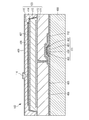
- FIG. 3C shows the detection pixel 101.
- the detection pixel 101 includes a photoelectric conversion element 115 included in a first conversion element that converts radiation into an electric signal, and a TFT 119 that is a first switch element that outputs an electric signal from the first conversion element to the detection signal line 104. ,including.
- a TFT 119 that is a first switch element that outputs an electric signal from the first conversion element to the detection signal line 104.
- the TFT 119 is turned on and off to acquire radiation irradiation information, such as measurement of illuminance when radiation is irradiated and detection of radiation irradiation start / end, and the signal accumulated in the photoelectric conversion element 115 is read out.
- the circuit 170 reads.
- FIG. 3D shows the correction pixel 108.
- the correction pixel 108 includes a photoelectric conversion element 123 included in a second conversion element that converts radiation into an electric signal, and a TFT 124 that is a second switch element that outputs an electric signal from the second conversion element to the correction signal line 103. ,including.
- the correction pixel 108 includes a shielding member 122 between a scintillator (not shown) disposed above the imaging region and the photoelectric conversion element 123. In the present embodiment, the correction pixel 108 and the photoelectric conversion element 123 arranged in the correction pixel 108 are entirely covered with the shielding member 122.
- the shielding member 122 By providing the shielding member 122, a difference occurs in the output value of the electrical signal with respect to the incident radiation between the photoelectric conversion element 115 of the detection pixel 101 and the photoelectric conversion element 123 of the correction pixel 108. That is, the correction pixel 108 is different in sensitivity to radiation from the detection pixel 101, and the sensitivity to incident radiation is lower than that of the correction pixel 108.
- Other structures may be the same as those of the detection pixel 101 illustrated in FIG. 3C.
- the charge generated in the photoelectric conversion element 120 is output to the detection signal line 104 in accordance with the capacitance formed between the detection signal line 104 and the photoelectric conversion element 120 of the pixel 110.
- a large number of such pixels 110 exist in the imaging region, and a signal written by capacitive coupling between the photoelectric conversion element 120 of the pixel 110 and the detection signal line 104 is not at a negligible level.
- the amount of signals due to capacitive coupling may be several times to several tens of times the electrical signal from the detection pixel 101.
- the photoelectric conversion element 120 does not overlap with the detection signal line 104, the charge from the photoelectric conversion element 120 is transferred due to the influence of the spread of the electric field or the like. Therefore, by arranging the correction signal line 103 in the adjacent region and acquiring the difference between the signals, the signal transferred from the photoelectric conversion element 120 is reduced and the signal from the detection pixel 101 is read out.
- the circuit 170 can read.
- FIG. 4 is a cross-sectional view taken along the line A-A ′ of the pixel 102 shown in FIG. 3A.
- Each pixel and each element are formed on the substrate 400 in the imaging region.
- an insulating substrate is used as the substrate 400.
- the substrate 400 for example, a glass substrate or a plastic substrate may be used.
- a TFT 111 which is a switch element is formed on the substrate 400.
- an inverted stagger type TFT is used.
- a top gate type TFT may be used.
- the TFT 111 includes a gate electrode 401, a source electrode 402, a drain electrode 403, and an insulating film 404.
- the insulating film 404 can function as a gate insulating film in the TFT 111.
- the photoelectric conversion element 120 is disposed via a protective film 405 and an interlayer insulating film 406.
- the photoelectric conversion element 120 includes a second impurity semiconductor layer 414 having a conductivity type opposite to that of the first impurity semiconductor layer 412, the intrinsic semiconductor layer 413, and the first impurity semiconductor layer 412 between the lower electrode 411 and the upper electrode 415. It has a structure laminated in this order.
- the impurity semiconductor layer 412, the intrinsic semiconductor layer 413, and the impurity semiconductor layer 414 constitute a PIN photodiode, and thereby perform photoelectric conversion.
- a PIN photodiode is used as a photoelectric conversion element.
- a MIS type element may be used.
- a power supply wiring 114 is disposed on the photoelectric conversion element 120 through a protective film 407 and an interlayer insulating film 408. The top of the pixel 102 is covered with a protective film 409. The power supply wiring 114 is connected to the upper electrode 415 of the photoelectric conversion element 120 through a contact plug.
- the lower electrode 411 of the photoelectric conversion element 120 is connected to the drain electrode 403 of the TFT 111.
- the charge generated by the photoelectric conversion element 120 by photoelectric conversion is output from the source electrode 402 to the image signal line 112 when the TFT 111 is turned on by the gate electrode 401 connected to the image control wiring 113.
- FIG. 5 is an equivalent circuit diagram showing a circuit configuration of the radiation imaging apparatus 100 in the present embodiment, and shows a modification of the circuit configuration shown in FIGS.
- the difference from the equivalent circuit diagrams shown in FIGS. 1 and 2 is that instead of the detection pixel 101 and the correction pixel 108, a detection pixel, an image pixel, a correction pixel, and an image pixel are respectively provided. That is, the paired pixels 131 and 132 are arranged. Other points may be the same as those of the radiation imaging apparatus 100 shown in FIGS.
- By disposing an image conversion element in an area where a conversion element for detecting radiation is also disposed it is possible to suppress pixel loss and facilitate image correction.
- FIG. 6 is a plan view of the pixel 131 and the pixel 132 shown in FIG.
- FIG. 6A shows a plan view of the pixel 131.
- the upper side of the pixel 131 has a configuration equivalent to that of the pixel 110, and includes a photoelectric conversion element 120 a having a smaller area than the photoelectric conversion element 120 of the pixel 110.
- the lower side of the pixel 131 has a configuration equivalent to that of the detection pixel 101, and includes a photoelectric conversion element 115 a having a smaller area than the photoelectric conversion element 115 of the detection pixel 101.
- FIG. 6B shows a plan view of the pixel 132.
- the upper side of the pixel 132 has a configuration equivalent to that of the pixel 110, and includes a photoelectric conversion element 120 a having a smaller area than the photoelectric conversion element 120 of the pixel 110.
- the lower side of the pixel 132 has a configuration equivalent to that of the correction pixel 108, and includes a photoelectric conversion element 123 a having a smaller area than the photoelectric conversion element 123 of the correction pixel 108.
- the area of the photoelectric conversion element 120a is about half the area of the photoelectric conversion element 120 of the pixels 102 and 110, but an output equivalent to that of the pixels 102 and 110 is obtained by image processing such as offset correction and gain correction. It becomes possible.
- the photoelectric conversion element 123 a and the TFT 124 arranged in the pixel 132 may have the same structure as the photoelectric conversion element 115 a and the TFT 119 arranged in the pixel 131. Since the conversion elements and the TFTs of the pixel 131 and the pixel 132 have the same structure, it is possible to correct an offset level and a dark current that are output from the conversion elements and the TFT, and that particularly change depending on the temperature. As a result, by subtracting the value of the electrical signal obtained from the correction signal line 103 from the value of the electrical signal obtained from the detection signal line 104, the radiation of the radiation applied to the detection pixel 101 is calculated from the difference. Information can be generated and acquired with high accuracy.
- FIG. 7 is a schematic layout diagram of the radiation imaging apparatus 100 in the present embodiment.
- the equivalent circuit diagrams shown in FIGS. 1, 2, and 5 represent a partial region of the radiation imaging apparatus as described above.
- FIG. 7 is a schematic layout diagram showing the entire radiation imaging apparatus 100. For example, 9 ⁇ 3 pixel areas having the equivalent circuit shown in FIG. 1 are provided.
- radiation information irradiated to each pixel area can be collected by the readout circuit 170 and the information processing circuit 180 of the signal processing circuit 171.
- FIG. 1 shows an example in which one detection pixel 101 and one correction pixel 108 are arranged in one pixel area, but FIG. 7 shows three detection pixels 101 and one in each pixel area. Correction pixels 108 are arranged.
- the number of detection pixels 101 connected to one detection signal line 104 may be the same as the number of correction pixels 108 connected to one correction signal line 103. Also, the sum of the numbers of pixels 110, detection pixels 101, and correction pixels 108 through which one detection signal line 104 passes, and the pixels 110, detection pixels 101, and correction pixels 108 through which one correction signal line 103 passes. The sum of the numbers should be the same.
- the detection pixel 101 and the correction pixel 108 may be arranged at the center of the imaging area away from the outer edge of the imaging area.
- the arrangement of the detection pixel 101 and the correction pixel 108 can be appropriately determined depending on the size and arrangement of the subject to be imaged.
- the three detection pixels 101 in each pixel area are connected to a common detection signal line 104, and the three correction pixels 108 are connected to a common correction signal line 103. Further, the detection signal line 104 and the correction signal line 103 are arranged so as to be shifted from each other so as not to be shared by different pixel areas. With such a configuration, for example, when the detection control wiring 116 is driven and signals from the detection pixel 101 and the correction pixel 108 are transferred to the signal processing circuit 171, all the detection control wirings 116 are operated simultaneously. It becomes possible to make it.
- the readout circuit 170 By operating simultaneously, it is possible to shorten the interval at which the readout circuit 170 reads out a signal for acquiring radiation irradiation information, compared with the case of reading out while scanning, and the readout speed is improved. If the reading speed does not need to be improved, for example, the detection signal line 104 and the correction signal line 103 are shared between the vertical pixel areas shown in FIG. 7, and the detection control wirings 116 are individually driven. Thereby, the processing circuit of the reading circuit 170 can be simplified, and the number of terminals connected to the reading circuit 170 can be reduced.
- FIG. 8 is a schematic layout diagram of the radiation imaging apparatus 100 in the present embodiment, and shows a modification of the schematic layout diagram shown in FIG. The difference from the layout shown in FIG. 7 is that the detection control wiring 116 is bundled for each pixel area before the detection control wiring 116 is connected to the driving circuit 160. With such a structure, the drive circuit 160 can be simplified, and the number of terminals connected to the drive circuit 160 can be reduced.
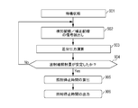
- FIG. 9 is a diagram illustrating a flowchart until the radiation imaging apparatus 100 according to the present embodiment detects radiation irradiation, determines the irradiation intensity, and outputs the irradiation stop time.
- the radiation imaging apparatus 100 maintains a standby state.
- the process proceeds to step 902.
- the electric signal transferred by the detection signal line 104 and the correction signal line 103 is sampled, and in step 903, the difference is extracted.
- the signal processing circuit 171 determines whether or not the radiation dose is stable based on the difference. If it is determined that the radiation dose is not stable, the signal processing circuit 171 returns to step 902. Proceed to 905.
- the signal processing circuit 171 calculates a time (irradiation stop time) at which radiation irradiation should be stopped based on the difference.
- the calculated irradiation stop time is transmitted from the signal processing circuit 171 to the controller that controls the radiation source in step 906.
- the controller stops the radiation irradiation based on the irradiation stop time.
- the radiation source is controlled by the signal processing circuit 171 of the radiation imaging apparatus 100, but is not limited thereto.
- the radiation imaging apparatus 100 may not calculate and output the irradiation stop time, but may output, for example, radiation information to be monitored, and stop determination may be performed by a tube that emits radiation and a control circuit that controls the tube. .
- FIG. 10 is a timing chart showing an operation controlled by the control unit 104 during radiation irradiation of the radiation imaging apparatus according to the present embodiment.
- the correction pixel 108 is described as having substantially no sensitivity to radiation.
- control signal ⁇ R is set to the high level, the reset switch R is turned ON, and the detection signal line 104 and the correction signal line 103 are reset. From the moment when the control signal ⁇ R is set to the low level and the reset switch R is turned off, the outputs from the detection signal line 104 and the correction signal line 103 start to change due to crosstalk.
- the control signal ⁇ S is turned on without turning on the detection pixels 101 and the correction pixels 108 (switch elements thereof) while the potential of the drive signal ⁇ Vd of the detection control wiring 116 is kept at a low level. After changing / H from low level to high level, the level is changed to low level again.
- the reading circuit 170 reads out the signals of the crosstalk components respectively appearing on the detection signal line 104 and the correction signal line 103 by sampling of each sample hold circuit S / H. A first operation as a set of reset and sampling is repeated once or a plurality of times.
- the readout circuit 170 outputs the crosstalk component signal CT1 (first signal) of the detection signal line 104 and the crosstalk component signal CT2 (second signal) of the correction signal line 103 one or more times. read out.
- the control signal ⁇ R is set to the high level, the reset switch R is turned ON, and the detection signal line 104 and the correction signal line 103 are reset. From the moment when the control signal ⁇ R is set to the low level and the reset switch R is turned off, the outputs from the detection signal line 104 and the correction signal line 103 start to change due to crosstalk. After that, the potential of the drive signal ⁇ Vd of the detection control wiring 116 is changed from the low level to the high level, and at least the detection pixel 101 and the correction pixel 108 (switch elements thereof) are turned on. Sampling the signal that appears. In the second period, the second operation which is a set of reset and sampling is repeated.
- the reading circuit 170 reads the signal S1 (third signal) including the radiation component signal and the crosstalk component signal from the detection pixel 101 appearing on the detection signal line 104 once or a plurality of times. Further, the reading circuit 170 reads the signal S2 (fourth signal) including the radiation component signal and the crosstalk component signal from the correction pixel 108 appearing on the correction signal line 103 once or a plurality of times. In the example shown in FIG. 10, since the correction pixel 108 does not substantially have sensitivity to radiation, the signal S2 does not substantially include the radiation component signal from the correction pixel 108. In the second operation, reset and sampling may be performed while the switch element of each pixel is turned on. Further, the switch element of each pixel may be maintained in the ON state during the second period.
- the information processing circuit 180 performs processing for generating information related to radiation irradiation based on the signal CT1, the signal CT2, the signal S1, and the signal S2.
- the information victory circuit 180 corrects the signal S1 based on the signal CT1, the signal CT2, and the signal S2, and performs processing for generating information related to radiation irradiation.
- the signal S1 can be corrected by calculating a ratio between the signal CT1 and the signal CT2 by the information processing circuit 180, correcting the signal S2 based on the ratio, and performing a difference process between the signal S1 and the corrected signal S2. . That is, the corrected signal S is obtained using the following equation (1).
- S S1-S2 * (CT1 / CT2) (1)
- the signal S1 is corrected by calculating the difference between the signal CT1 and the signal CT2 by the information processing circuit 180, correcting the signal S2 based on the difference, and performing differential processing between the signal S1 and the corrected signal S2. Can be made. That is, the corrected signal S is obtained using the following equation (2).
- S S1- (S2- (CT1-CT2)) (2)
- the radiation dose per unit time must be stable. That is, if the radiation dose per unit time in the first operation and the radiation dose per unit time in the second operation are substantially equal, correction using the equation (2) is possible. .
- the signal difference including the dark current and the offset level can be used as the correction value, so the dark current and the offset level are also subtracted in the second period. It is possible.
- the first period is preferably performed immediately after the start of radiation irradiation and between the start of the second period in order to start generating information related to radiation irradiation quickly.
- the first period is performed at any timing during radiation irradiation and the obtained output is corrected even if the second period is provided before the first period from the signal obtained there, It is possible to obtain the effect of this embodiment.
- the correction pixel 108 has been described as having substantially no sensitivity to radiation.
- the present invention is not limited to this, and as shown in FIG. It is also possible to use the one having sensitivity to radiation 108.
- FIG. 11 shows an example in which the correction pixel 108 having lower sensitivity than the detection pixel 101 is used.
- the operation cycle of the first operation that is performed a plurality of times and the operation cycle of the second operation that is performed a plurality of times have been described.
- the present invention is not limited thereto.
- the operation cycle of the first operation performed a plurality of times is shorter than the operation cycle of the second operation performed a plurality of times, that is, the first operation can be performed at a higher speed than the second operation. .
- more sampling can be performed per unit time than in the example of FIG. 10, and the correction accuracy can be further improved.
- Expression (1) can be applied as it is.
- the correction can be performed by multiplying the difference between the signal CT1 and the signal CT2 by the ratio of the respective operation cycles.
- it may be acquired in advance at a plurality of different sampling intervals, and the difference may be corrected using calibration data.
- the conversion element, the scintillator, and the TFT may be different materials or configurations, or may be a conversion element that directly detects radiation.
- the entire structure of the photoelectric conversion elements 123 and 123 a is shielded.
- the photoelectric conversion elements 123 and 123a may be provided in the upper part of the substrate so that part of the light reaches the conversion element.
- one of the detection signal line 104 and the correction signal line 103 from which a signal is output from the detection pixel 101 and the correction pixel 108 is also used as an image signal line from which a signal is output from the conversion element of the pixel 102. It may be a dual-purpose signal line.
- X-rays 6060 generated by an X-ray tube 6050 serving as a radiation source pass through a chest 6062 of a patient or subject 6061 and enter the radiation imaging apparatus 100 of the present invention.
- This incident X-ray includes information inside the body of the patient or subject 6061.
- the scintillator emits light in response to the incidence of the X-ray 6060, and this is photoelectrically converted by the photoelectric conversion element to obtain electrical information.
- This information is converted into digital data, image-processed by an image processor 6070 as a signal processing unit, and can be observed on a display 6080 as a display unit of a control room. Further, this information can be transferred to a remote place by a transmission processing unit such as a telephone line 6090. In this way, it can be displayed on a display 6081 which is a display unit such as a doctor room in another place, and a doctor in a remote place can make a diagnosis. In addition, this information can be recorded on a recording medium such as an optical disk, and can also be recorded on a film 6110 serving as a recording medium by the film processor 6100. Note that the X-ray tube 6050 can be controlled to stop radiation irradiation based on information regarding radiation irradiation generated by the information processing circuit included in the radiation imaging apparatus of the present invention.
Landscapes
- Health & Medical Sciences (AREA)
- Life Sciences & Earth Sciences (AREA)
- Engineering & Computer Science (AREA)
- Physics & Mathematics (AREA)
- High Energy & Nuclear Physics (AREA)
- Molecular Biology (AREA)
- Medical Informatics (AREA)
- Radiology & Medical Imaging (AREA)
- Animal Behavior & Ethology (AREA)
- Biophysics (AREA)
- Spectroscopy & Molecular Physics (AREA)
- Nuclear Medicine, Radiotherapy & Molecular Imaging (AREA)
- Optics & Photonics (AREA)
- Pathology (AREA)
- General Physics & Mathematics (AREA)
- Biomedical Technology (AREA)
- Heart & Thoracic Surgery (AREA)
- Surgery (AREA)
- Veterinary Medicine (AREA)
- General Health & Medical Sciences (AREA)
- Public Health (AREA)
- Multimedia (AREA)
- Signal Processing (AREA)
- Computer Vision & Pattern Recognition (AREA)
- Mathematical Physics (AREA)
- Measurement Of Radiation (AREA)
- Apparatus For Radiation Diagnosis (AREA)
- Transforming Light Signals Into Electric Signals (AREA)
Abstract
第1スイッチ素子を含む第1検出用画素及び第2スイッチ素子を含み第1検出用画素とは放射線を検出する感度が異なる第2検出用画素と、導通状態の第1スイッチ素子を介して信号が出力される第1信号線及び導通状態の第2スイッチ素子を介して信号が出力される第2信号線と、放射線撮像装置に放射線が照射されている期間に、第1及び第2スイッチ素子を導通しない状態で第1及び第2信号線に現れる第1及び第2信号を読み出す第1動作と、第1及び第2スイッチ素子が導通することによって第1及び第2信号線に現れる第3及び第4信号を読み出す第2動作と、を行う読出し回路と、第1乃至第4信号に基づいて放射線照射に関する情報を生成する処理を行う情報処理回路と、を含む。
Description
本発明は、放射線撮像装置及び放射線撮像システムに関する。
放射線を電荷に変換する変換素子と薄膜トランジスタ(TFT)などのスイッチ素子とを組み合わせた画素が2次元アレイ状に配列された放射線撮像装置が、広く利用されている。近年、こうした放射線撮像装置の多機能化が検討され、その1つとして自動露出制御(AEC)機能の内蔵が検討されている。AEC機能は、放射線源が放射線を照射している間、放射線撮像装置が照射情報を取得する手段として利用される。
特許文献1には、撮像領域にアレイ状に配置され放射線画像を取得するための複数の画素を含む放射線撮像装置が開示されている。また、特許文献1の放射線撮像装置は、撮像領域又は撮像領域に隣接し配され放射線の照射に関する情報を取得するために放射線を電気信号に変換するための変換素子を含む検出用画素を含む。更に、特許文献1の放射線撮像装置は、検出用画素から信号が出力される検出信号線と、検出用画素から検出信号線を介して出力される信号を処理する信号処理回路と、を含む。検出用画素及び検出信号線は、放射線の照射の開始、照射の終了、累計の放射線の照射量といった、放射線の照射に関する情報の検出に利用される。このような放射線撮像装置において、放射線画像を取得するための画素の電極と検出信号線との間に無視できない寄生容量が存在する。この寄生容量を介して、放射線照射によって生じる放射線画像を取得するための画素の電極の電位変動により、クロストークが発生し得る。検出信号線に流れる信号には、放射線画像を取得するための画素からの信号の成分と、クロストークによって発生した成分とが含まれる。このクロストークの成分によって、放射線照射中に放射線検出用画素からの信号を正確に取得することが難しい。そこで、特許文献1の放射線撮像装置は、検出用画素とは放射線を検出する感度が異なる補正用画素と、撮像領域又は撮像領域に隣接し配され補正用画素から信号が出力される補正信号線と、を更に含む。そして、特許文献1の放射線検出装置では、信号処理回路は、検出信号線からの信号と補正信号線からの信号とに基づいて、クロストークによる影響が低減するように補正された放射線の照射に関する情報を生成する。
しかしながら、特許文献1の放射線撮像装置で得られた放射線の照射に関する情報は、補正の精度に課題を残す。検出信号線に係る複数の画素の寄生容量と、補正信号線に係る複数の画素の寄生容量と、に相違があると、検出信号線の信号に重畳するクロストークと補正信号線の信号に重畳するクロストークとに相違が生じる。これは、補正信号線には補正用画素が接続されることにより、補正信号線に係る複数の画素の個数が検出信号線に係る複数の画素の個数と相違し得ることに起因する。この相違の影響を低減することが、補正の精度向上に必要となる。また、撮影毎に照射放射線の強度の面内分布が異なるが、照射放射線の強度が高い領域における、検出用画素の個数と感度が異なる補正用画素の個数に依存して、各配線で発生するクロストークも異なる場合がある。そのため、撮影毎に発生するクロストークの相違の影響を低減することが、補正の精度向上に必要となる。
本発明は、クロストークに起因する信号の変化を補正し、その補正の精度を向上させることにより放射線の検出の正確性を向上する技術を提供することを目的とする。
上記課題に鑑みて、本発明の実施形態に係る放射線撮像装置は、撮像領域にアレイ状に配置され放射線画像を取得するための複数の画素と、放射線の照射の開始、放射線の照射の終了、放射線の照射強度、及び、放射線の照射量のうち少なくとも1つを含む、前記撮像領域に対する放射線の照射に関する情報を取得するために、第1スイッチ素子を含む第1検出用画素、及び、第2スイッチ素子を含み前記第1検出用画素とは放射線を検出する感度が異なる第2検出用画素と、前記撮像領域又は前記撮像領域に隣接し配され、導通状態の前記第1スイッチ素子を介して前記第1検出用画素から信号が出力される第1信号線、及び、導通状態の前記第2スイッチ素子を介して前記第2検出用画素から信号が出力される第2信号線と、前記放射線撮像装置に前記放射線が照射されている期間に、前記第1及び第2スイッチ素子を導通しない状態で前記第1及び第2信号線に現れる第1及び第2信号を読み出す第1動作と、前記第1及び第2スイッチ素子が導通することによって前記第1及び第2信号線に現れる第3及び第4信号を読み出す第2動作と、を行う読出し回路と、前記第1乃至第4信号に基づいて前記情報を生成する処理を行う情報処理回路と、を含むことを特徴とする。
上記手段により、クロストークに起因する信号の変化に対する補正の精度を向上し、放射線の検出の正確性を向上する技術が提供される。
以下、本発明に係る放射線撮像装置の具体的な実施形態を、添付図面を参照して説明する。なお、以下の説明及び図面において、複数の図面に渡って共通の構成については共通の符号を付している。そのため、複数の図面を相互に参照して共通する構成を説明し、共通の符号を付した構成については適宜説明を省略する。なお、本発明における放射線には、放射線崩壊によって放出される粒子(光子を含む)の作るビームであるα線、β線、γ線などの他に、同程度以上のエネルギーを有するビーム、例えばX線や粒子線、宇宙線なども含みうる。
図1~9を参照して、第1実施形態による放射線撮像装置について説明する。図1は、本実施形態における放射線撮像装置100の回路構成を示す等価回路図である。本実施形態における放射線撮像装置100は、基板上に複数の画素がアレイ状に配された撮像領域と、各画素の制御や各画素から出力された電気信号を処理するための周辺領域とを含む。
周辺領域は、各画素を駆動、制御するための電源回路150及び駆動回路160と、各画素から出力された電気信号を処理するための読出し回路170及び情報処理回路180を含む信号処理回路171とを含むが、これに限られるものではない。例えば読出し回路170と情報処理回路180とは、一体で構成されていてもよい。また、放射線撮像装置100の周辺領域は、信号処理部171を制御するための制御回路140を更に含む。
撮像領域には、放射線画像を取得するため複数の画素と、放射線の照射の検出や照射情報を取得するための複数の検出用画素とを含む。本実施形態において、画素は、画素内の配線の配置によって画素102と、検出用画素で得られた電気信号を信号処理回路171に転送する信号線が画素内を通過する画素110とを含む。また検出用画素は、互いに異なる信号線によって信号処理回路に電気信号を出力する第1検出用画素である検出用画素101と、第2検出用画素である補正用画素108とを含む。検出用画素101及び補正用画素108は、放射線が照射される際、放射線画像とは別の、放射線の照射の開始や放射線の照射の終了、また放射線の照射強度や放射線の照射量などの放射線の照射に関する情報である放射線照射情報を取得するために使用される。このような検出用画素101及び補正用画素108を配置することによって、自動露出制御(AEC)機能を、放射線撮像装置100に内蔵することが可能となる。図1には、撮像領域に5行5列の画素が設けられているが、これらは放射線撮像装置100のうち一部の撮像領域を表した等価回路である。
撮像領域には、このような検出用画素101及び補正用画素108の配された画素エリアが、1つだけ配置されてもよいし、また複数、配置されてもよい。放射線撮像装置100において、検出用画素101や補正用画素108の配置された画素エリアが、例えば3×3や5×5のマトリックス状に配置される。これによって、放射線撮像装置100の各画素エリアに照射される放射線の照射情報を、画素エリアごとに個別に検出することが可能となる。複数の画素エリアを有する撮像領域については、図8、9を用いて後述する。
放射線撮像装置100の撮像領域に配された画素102、110は、電源回路150から電源配線114を介して電源が供給され、駆動回路160から画像制御配線113を介して制御される。また画素102、110から出力される電気信号は、画像信号線112によって信号処理回路171に転送される。これによって放射線画像の取得が可能となる。また検出用画素101及び補正用画素108は、電源回路150から電源配線114を介して電源が供給され、駆動回路160から検出制御配線116を介して制御される。検出用画素101から出力される電気信号は、第1信号線である検出信号線104によって信号処理回路171に転送される。また補正用画素108から出力される電気信号は、第2信号線である補正信号線103によって信号処理回路171に転送される。検出用画素101、補正用画素108を用いて放射線の照射情報を取得することによって、検出用画素101、補正用画素108の配置された領域の放射線量などの照射情報を取得することが可能となる。本実施形態において、検出信号線104及び補正信号線103は撮像領域内に配される。検出信号線104及び補正信号線103は、撮像領域の外縁部に隣接して配されてもよい。また、検出信号線104及び補正信号線103は、複数の画像信号線112のうちの一部の画像信号線112と同一であってもよい。また、検出制御用配線116は、画像制御配線113のうちの一部の画像制御配線113と同一であってもよい。ここで、読出し回路170は、検出信号線104及び補正信号線103をリセットするためにそれぞれに接続されたリセットスイッチRを含む。また、読出し回路170は、検出信号線104を介して検出用画素101から出力される電気信号を、読出し回路170が読み出すためにサンプルホールドするためのサンプルホールド回路S/Hを含む。また、読出し回路170は、補正信号線103を介して補正用画素108から出力される電気信号を、読出し回路170が読み出すためにサンプルホールドするためのサンプルホールド回路S/Hを含む。制御回路140は、リセットスイッチRを制御するための制御信号ΦRをリセットスイッチRに供給する。また、制御回路140は、各サンプルホールド回路S/Hを制御するための制御信号ΦS/Hを各サンプルホールド回路S/Hに供給する。
放射線撮像装置100において、放射線は検出用画素101や補正用画素108以外の部位にも照射される。放射線が照射されると画素102、110においても、照射される放射線の量に応じた電荷が発生し蓄積される。このとき検出信号線104の通過する画素110において、この蓄積された電荷は、放射線を電荷に変換する画素110の変換素子の電極と検出信号線104との間に存在する寄生容量を介し、電荷保存則に基づき検出信号線104に転送される。この結果、検出信号線104から読み出される電気信号である電荷量は、検出用画素101からの電荷と、検出信号線104と画素110の変換素子との間の容量を介して画素110から転送される電荷との2つの成分を含んでしまう。このことから、例えば放射線の照射面積が広くなり、放射線の照射される画素110の数が多くなると、画素110から検出信号線104に転送される電荷量が多くなる。また例えば、放射線の照射面積が狭くなり、放射線の照射によって電荷を多く蓄積した画素110が少なくなると、画素110から検出信号線104に転送される電荷量が少なくなる。
この検出信号線104と通過する画素110との容量を介した電荷の転送を補正し、検出用画素101に照射された放射線の量に対応した電気信号を読出し回路170が正しく読み出すために、補正信号線103が用いられる。例えば、補正信号線103と検出信号線104との形状や通過する画素110の数が同等の場合、画素110と補正信号線103又は検出信号線104との間に存在する寄生容量は、ほぼ等しくなる。この結果、画素110から補正信号線103及び検出信号線104に転送される電荷の量は、ほぼ等しくなる。検出信号線104によって取得された電気信号の値である電荷量から、補正信号線103からの電気信号の値である電荷量を減算する。この減算(差分処理)で、検出用画素101で変換された電荷量と同等の電荷量を、検出用画素101の信号の情報として生成し、取得することができる。ここで減算の方法は、さまざまの方法を用いることが可能である。例えばアナログ減算を用いてもよいし、デジタル減算を用いてもよい。また例えば相関二重サンプリング(CDS)回路を用いてもよい。
しかしながら、例えば撮像領域の周辺に配置された信号処理回路171などが、信号処理に際して発熱する。局所的な発熱によって、画素102、110や検出用画素101が配置された撮像領域は、温度やその温度分布は一様ではなく変化する可能性がある。画素102、110及び検出用画素101内に配置される変換素子やスイッチ素子である薄膜トランジスタ(TFT)は、温度が変化すると変換素子のダーク電流やTFTのオフセットレベルなどの特性が変化してしまう場合がある。放射線を検出する際、検出用画素101はオン動作し、画素102、110のTFTはオフとなる。このとき補正信号線103と検出信号線104との間の電気信号の差分には、入射する放射線に起因する成分だけでなく、オン動作する検出用画素101のオフセットレベルやダーク電流などの特性の変動成分が重畳される。検出用画素101のダーク電流やオフセットレベルの特性が変化すると、差分によって取得される電気信号の値も変化する。例えば、温度上昇によって検出用画素101のオフセットレベルが増大した場合、放射線の照射がない場合でも、抽出された電気信号が放射線を検出するための閾値を越えてしまう可能性がある。この場合、放射線の照射がなくても、放射線が照射されたと認識してしまう。
これに対して、本実施形態において検出信号線104に接続されている検出用画素101と同一の変換素子の構造や同一のTFTの構造を有し、補正信号線103に接続される補正用画素108を、放射線撮像装置100の撮像領域に配置する。補正用画素108は、検出用画素101と同時にオン動作するとよい。図1において、補正用画素108と検出用画素101とは、同じ検出制御配線116を介して制御され、駆動信号ΦVdにより同時にオン動作する。また、補正用画素108は、検出用画素101の近傍に配置されるとよい。撮像領域の検出用画素101の周囲の温度や温度分布が変化し、画素102、110や検出用画素101においてダーク電流やオフセットレベルなどの特性が変化する。しかし近傍に配置した同等の温度特性を有する補正用画素108を配することによって、検出用画素101のダーク電流やオフセットレベルなどの特性が変動した場合でも、ダーク電流やオフセットレベルなどを減算することができる。結果として、検出用画素101に照射される放射線の照射に関する情報を精度よく生成し、取得することが可能となる。
しかし、補正用画素108と検出用画素101とは、先述したように同一の構造の変換素子やTFTを有するため、補正用画素108と検出用画素101とで入射する放射線の量に対して出力される電気信号である電荷量の差が小さい。補正用画素108と検出用画素101とからの出力の差が小さい場合、検出信号線104と補正信号線103との電荷量の差分を求めるだけで、検出用画素101の信号の情報を取得することは難しい。放射線の照射に関する情報を生成するため、検出用画素101と補正用画素108とは、同一の変換素子の構造や同一のTFTの構造を有しながら、入射する放射線に対して異なる電気信号を出力する必要がある。異なる電気信号を出力するために、入射する放射線を電気信号に変換する感度が、検出用画素101と補正用画素108とで異なるとよい。本実施形態において、検出用画素101と補正用画素108とで、放射線を検出するための領域の大きさが異なり、検出用画素101の方が、補正用画素108よりも放射線を検出する領域が大きくなるように形成される。例えば放射線を直接、電気信号に変換する放射線撮像装置の場合、放射線を遮る遮蔽部材として、例えば鉛などの重金属を用いた遮蔽部材を補正用画素108の変換素子の上に設けてもよい。またシンチレータを用いて放射線を光に変換し、この光を電気信号に変換する間接型の放射線撮像装置の場合、光を遮る遮蔽部材として例えばアルミニウムの遮蔽膜などを補正用画素108の変換素子とシンチレータとの間に設けてもよい。何れの変換型の放射線撮像装置であっても、遮蔽部材が、撮像領域に対する平面視において、補正用画素108の変換素子の少なくとも一部と重なる領域に配されるとよい。この結果、検出用画素101よりも、補正用画素108の放射線を電気信号に変換する感度が低いこととなる。これによって、画素110と検出用画素101との間の寄生容量だけでなく、動作温度が変化し各素子の特性が変動した場合でも、放射線の照射に関する情報を検出信号線104と補正信号線103とから得られる電気信号の減算によって、より正確に生成できる。
例えば、シンチレータを用いた間接型の放射線撮像装置の場合、補正用画素108は、検出用画素101と大きさや変換素子、TFTの構造を同一とし、変換素子よりも放射線が入射する側に光を遮る例えばアルミニウムやクロムなどを用いた遮蔽部材を形成する。遮蔽部材は、例えばシンチレータと変換素子との間に配置すればよい。また、例えば補正用画素108の全体を遮蔽膜で覆い、検出する光をほぼゼロとし、変換素子のダーク電流や、TFT部分のオフセットレベルなどを取得し、この値を用いて検出用画素101の補正を行ってもよい。
検出用画素101と補正用画素108とは、互いに隣接していてもよい。また検出用画素101と補正用画素108との間に画素102を数列、例えば図1に示すように2列配置してもよい。これは、検出用画素101と補正用画素108とを互いに隣接して配置した場合、間に検出用画素101と補正用画素108とが配される画素102同士の間隔が広くなる。検出用画素101と補正用画素108との間に画素102を挿入することによって、画素の欠落する検出用画素101及び補正用画素108の部分の画像の補正が容易となる。放射線撮像装置100に用いる画素の各辺のサイズは、例えば50μm~500μm程度と小さい。間に2つの画素102が配された場合でも、検出用画素101と補正用画素108との相対距離は150μm~1.5mm程度と近い距離にあり、検出用画素101と補正用画素108との温度環境は同等とみなすことができる。検出用画素101と補正用画素108との間に数列の画素102を配した場合でも、精度よく放射線の照射に関する情報を生成し、取得することができる。ただし、検出信号線104に係る複数の画素102の寄生容量と、補正信号線103に係る複数の画素102の寄生容量と、に相違があると、検出信号線104の信号に重畳するクロストークと第2信号線の信号に重畳するクロストークとに相違が生じる。これは、補正信号線103には補正用画素108が接続されることにより、補正信号線103に係る複数の画素102の個数が検出信号線104に係る複数の画素の個数と相違し得ることに起因する。この相違の影響を低減することが、補正の精度向上に必要となる。また、撮影毎に照射放射線の強度に面内分布が異なるが、照射放射線の強度が高い領域における補正用画素108の個数により発生するクロストークも異なる場合がある。例えば、補正信号線103に係る遮光されている補正用画素が、照射放射線の強度が高い領域に存在する場合、各配線に係る電極が電位変動を起こす画素の個数が、補正信号線103と検出信号線104で異なる。この結果、補正信号線103と検出信号線104で発生するクロストークが異なってしまう。そのため、撮影毎に発生するクロストークの相違の影響を低減することが、補正の精度向上に必要となる。
図2は、本実施形態における放射線撮像装置100の回路構成を示す等価回路図で、図1に示した回路構成の変形例を示したものである。図1に示した等価回路図と異なる点は、検出用画素101と補正用画素108とを制御する検出制御配線116を、画素102、110を制御する駆動回路160とは別に設けたAEC制御回路190を用いて駆動信号ΦVdを供給することにより制御することである。これ以外の点は、図1に示した等価回路図と同じ回路構成であってよい。これによって、駆動回路160が、図1に示した放射線撮像装置100の駆動回路160と比較して複雑な動作を必要としなくなり、駆動回路の設計が容易となる。例えば放射線が照射され、検出用画素101及び補正用画素108で放射線の照射情報を読み取るまでの期間は、AEC制御回路190を駆動させる。次いで、画素102、110から放射線画像を取得するための信号を読出し回路170が読み出す際は、AEC制御回路190を停止し、駆動回路160を駆動させて行ごとに順次、信号を読み出してもよい。また検出用画素101及び補正用画素108と、画素102、110とに対して別々に周辺領域の回路を動作させるのは、AEC制御回路190に限定されるものではない。例えば信号処理回路171の読出し回路170において、検出信号線104や補正信号線103からの信号と、画素102、110とは別の読出し回路を設けて処理してもよい。
図3に、画素102、110、検出用画素101、補正用画素108の平面図を示す。図3Aは、画素102の平面図を示す。本実施形態において、放射線撮像装置100は、間接型の放射線撮像装置であり、画素102、110、検出用画素101、補正用画素108などの配された撮像領域の上部にシンチレータ(不図示)が配される。画素102には、シンチレータで放射線から変換された光を電気信号に変換するための変換素子である光電変換素子120が配置される。光電変換素子120の下部には、スイッチ素子である薄膜トランジスタ(TFT)111や各種配線が配置される。光電変換によって光電変換素子120で生成された電気信号は、画像制御配線113の信号によってTFT111がON状態となったとき、TFT111を介して画像信号線112に出力される。光電変換素子120の上部電極は、一定の電圧を印加するための電源配線114と接続される。検出制御配線116は、光電変換素子120の下部を通過する。図1、2に示されるように、検出制御配線116が通過しない画素102も存在するが、図3Aには、検出制御配線116が通過する画素102を図示している。
図3Bは、画素内に検出信号線104又は補正信号線103が通過する画素110を示す。検出信号線104又は補正信号線103が通過する以外の点は、画素102と同じであってよい。画素102、110に配される光電変換素子120の下部電極は、画素ごとに個別の電極となっている。このため、撮像領域に対する平面視において、画素110を通過する検出信号線104又は補正信号線103と、光電変換素子120の下部電極との重なる領域にオーバーラップ面積に応じた容量が形成される。この容量を介して、電荷保存則に基づき、光電変換素子120に蓄積された電荷が、検出信号線104又は補正信号線103に転送される。
図3Cは、検出用画素101を示す。検出用画素101は、放射線を電気信号に変換する第1変換素子に含まれる光電変換素子115と、第1変換素子からの電気信号を検出信号線104に出力する第1スイッチ素子であるTFT119と、を含む。光電変換素子115の下部電極がTFT119を介して検出信号線104に接続され、検出制御配線116の信号によってTFT119がON状態(導通状態)となったとき、光電変換素子115からの電気信号が検出信号線104に出力される。放射線が照射された際の照度の測定や、放射線の照射開始・終了の検出など、放射線の照射情報の取得のためにTFT119をON/OFF動作させ、光電変換素子115に蓄積された信号を読出し回路170が読み出す。
図3Dは補正用画素108を示す。補正用画素108は、放射線を電気信号に変換する第2変換素子に含まれる光電変換素子123と、第2変換素子からの電気信号を補正信号線103に出力する第2スイッチ素子であるTFT124と、を含む。補正用画素108は、撮像領域の上部に配されたシンチレータ(不図示)と光電変換素子123との間に遮蔽部材122を有する。本実施形態において、補正用画素108及び補正用画素108に配置された光電変換素子123は、全体が遮蔽部材122に覆われる。遮蔽部材122を配することによって、検出用画素101の光電変換素子115と、補正用画素108の光電変換素子123との間で、入射した放射線に対する電気信号の出力値に差が生じる。すなわち、補正用画素108は、検知用画素101と放射線に対する感度が異なり、入射した放射線に対する感度が補正用画素108より低いこととなる。これ以外の構造は、図3Cに示す検出用画素101と同様であってよい。光電変換素子123の下部電極がTFT124を介して補正信号線103に接続され、検出制御配線116の信号によってTFT124がON状態(導通状態)となったとき、光電変換素子123からの電気信号が補正信号線103に出力される。
上述したように、検出信号線104と画素110の光電変換素子120との間で形成される容量に応じて、光電変換素子120で発生した電荷が、検出信号線104に出力されてしまう。このような画素110は、撮像領域中に多数存在し、画素110の光電変換素子120と、検出信号線104との容量結合によって書き込まれる信号は無視できるレベルではない。例えば、このような画素110が数百から数千といった数存在する場合、容量結合による信号の量が、検出用画素101からの電気信号の数倍から数十倍といった量になる場合がある。また例えば、光電変換素子120が検出信号線104とオーバーラップしていない場合であっても、電界の広がりなどの影響で、光電変換素子120からの電荷が転送される。そこで、近接する領域に補正信号線103を配置し、それぞれの信号の差分を取得することによって、このような光電変換素子120から転送される信号を低減し、検出用画素101からの信号を読出し回路170が読み出すことが可能となる。
図4に、図3Aに示した画素102のA-A’間の断面図を示す。撮像領域の基板400の上に各画素や各素子が形成される。本実施形態において、基板400として絶縁基板を用いる。基板400として、例えばガラス基板やプラスチック基板を用いてもよい。基板400の上にスイッチ素子であるTFT111が形成される。本実施形態において逆スタガ型のTFTを用いるが、例えばトップゲート型のTFTを用いてもよい。TFT111は、ゲート電極401、ソース電極402、ドレイン電極403、絶縁膜404を含む。絶縁膜404は、TFT111においてゲート絶縁膜として機能しうる。TFT111の上には、保護膜405及び層間絶縁膜406を介して光電変換素子120が配置される。光電変換素子120は、下部電極411と上部電極415との間に、第1不純物半導体層412、真性半導体層413、第1不純物半導体層412とは逆の導電型の第2不純物半導体層414がこの順番に積層された構造を有する。不純物半導体層412と真性半導体層413と不純物半導体層414とは、PINフォトダイオードを構成し、これによって光電変換を行う。本実施形態においてPINフォトダイオードを光電変換素子に用いるが、例えばMIS型素子を用いてもよい。また光電変換素子120の上には、保護膜407及び層間絶縁膜408を介して電源配線114が配される。画素102の上は、保護膜409で覆われる。電源配線114は、コンタクトプラグを介して光電変換素子120の上部電極415に接続される。光電変換素子120の下部電極411は、TFT111のドレイン電極403と接続される。光電変換によって光電変換素子120で生成された電荷は、画像制御配線113に接続されたゲート電極401によってTFT111がON動作したとき、ソース電極402から画像信号線112へと出力される。
図5は、本実施形態における放射線撮像装置100の回路構成を示す等価回路図で、図1、2に示した回路構成の変形例を示したものである。図1、2に示した等価回路図と異なる点は、検出用画素101、補正用画素108に代えて、検出用画素と画像用の画素と、補正用画素と画像用の画素とを、それぞれ対にした画素131、132を配したことである。これ以外の点は、図1、2に示した放射線撮像装置100と同じであってよい。放射線を検出するための変換素子を配置した領域にも画像用の変換素子を配置することによって、画素の欠落を抑制し、画像の補正を容易にすることが可能となる。
図6は、図5に示した画素131及び画素132の平面図を示す。図6Aに画素131の平面図を示す。画素131の上側は画素110と同等の構成を有し、画素110の光電変換素子120よりも面積の小さい光電変換素子120aを有する。画素131の下側は検出用画素101と同等の構成を有し、検出用画素101の光電変換素子115よりも面積の小さい光電変換素子115aを有する。また図6Bに画素132の平面図を示す。画素132の上側は画素110と同等の構成を有し、画素110の光電変換素子120よりも面積の小さい光電変換素子120aを有する。画素132の下側は補正用画素108と同等の構成を有し、補正用画素108の光電変換素子123よりも面積の小さい光電変換素子123aを有する。光電変換素子120aの面積は、画素102、110の光電変換素子120の約1/2程度の面積になるが、オフセット補正やゲイン補正などの画像処理によって、画素102、110と同等の出力を得ることが可能となる。また画素132に配置される光電変換素子123a及びTFT124は、画素131に配置される光電変換素子115a及びTFT119と同一の構造を有してよい。画素131及び画素132の変換素子やTFTが同一の構造を有することによって、変換素子やTFTから出力される、特に温度によって変化するオフセットレベルやダーク電流を補正することができる。結果として、検出信号線104から得られた電気信号の値から、補正信号線103から得られた電気信号の値を減算することによって、その差分から検出用画素101に照射された放射線の照射に関する情報を精度よく生成し、取得することが可能となる。
図7は、本実施形態における放射線撮像装置100の概略レイアウト図である。図1、2、5で示した等価回路図は、前述のように放射線撮像装置の一部の領域を表した図である。図7は、放射線撮像装置100の全体を表した概略レイアウト図で、例えば、図1に示した等価回路を有する画素エリアが、3×3の9領域設けられている。また、各画素エリアに照射された放射線情報を、信号処理回路171の読出し回路170及び情報処理回路180で収集することが可能となる。図1では、1つの画素エリア内に検出用画素101と補正用画素108とが1つずつ配置された例を示したが、図7では1つの画素エリア内にそれぞれ3つの検出用画素101と補正用画素108とが配置されている。1つの検出信号線104に接続される検出用画素101の数と、1つの補正信号線103に接続される補正用画素108の数とが同じであるとよい。また1つの検出信号線104が通過する画素110、検出用画素101、補正用画素108の数の総和と、1つの補正信号線103が通過する画素110、検出用画素101、補正用画素108の数の総和とが同じであるとよい。接続される検出用画素101や補正用画素108の数、通過する画素110、検出用画素101、補正用画素108の数を同等にすることによって、検出用画素101に照射された放射線の照射に関する情報を精度よく取得することが可能となる。また例えば画素エリアEのように、検出用画素101及び補正用画素108は、撮像領域の外縁部から離れ、撮像領域の中心部に配置されてもよい。検出用画素101及び補正用画素108の配置は、撮像対象となる被検体の大きさや配置によって、適宜決めることができる。
各画素エリアの3つの検出用画素101は、共通の検出信号線104に接続されており、3つの補正用画素108は共通の補正信号線103に接続されている。また検出信号線104と補正信号線103とが、異なる画素エリア同士で共用しないように列をずらして配置されている。このような構成にすることで、例えば検出制御配線116を駆動させ、検出用画素101と補正用画素108とからの信号を信号処理回路171へ転送させる際、全ての検出制御配線116を同時に動作させることが可能となる。同時に動作させることによって、走査しながら読み出した場合と比較して、放射線の照射情報を取得するための信号を読出し回路170が読み出す間隔を短くすることが可能となり、読み出しの速度が向上する。また読み出し速度の向上が必要ない場合は、例えば図7に示す上下方向の画素エリア間で検出信号線104と補正信号線103を共通化し、検出制御配線116を個別に駆動させる。これによって、読出し回路170の処理回路を簡素化でき、更に読出し回路170と接続する端子数を減らすことができる。
図8は、本実施形態における放射線撮像装置100の概略レイアウト図で、図7に示した概略レイアウト図の変形例を示したものである。図7に示したレイアウトと異なる点は、検出制御配線116を駆動回路160に接続する手前で画素エリアごとに束ねている点である。このような構成にすることによって、駆動回路160を簡素化でき、駆動回路160と接続する端子数を減らすことができる。
図9は、本実施形態における放射線撮像装置100が、放射線照射を検出し照射強度を判定し照射停止時間を出力するまでのフローチャートを示した図である。ステップ901において、放射線撮像装置100は、待機状態を維持する。放射線の照射が開始されると、ステップ902に進む。ステップ902では、検出信号線104及び補正信号線103によって転送される電気信号をサンプリングし、ステップ903において差分を抽出する。ステップ904では、信号処理回路171は、差分に基づいて放射線の照射量が安定したか否かを判定し、安定していないと判断した場合はステップ902に戻り、安定したと判断した場合はステップ905に進む。ステップ905では、信号処理回路171は、差分に基づいて放射線の照射を停止させるべき時刻(照射停止時間)を算出する。算出された照射停止時間は、ステップ906で信号処理回路171から放射線源を制御するコントローラに送信される。コントローラは、この照射停止時間に基づいて、放射線の照射を停止する。本実施形態において、放射線撮像装置100の信号処理回路171によって、放射線源の制御が行われるが、これに限られるものではない。放射線撮像装置100から、照射停止の時間の算出と出力を行わず、例えばモニタする放射線情報を出力し、停止判断は放射線を照射する管球及び管球を制御する制御回路で行っても構わない。
次に、図10を用いて、図9のステップ902からステップ905で行われる放射線撮像装置の動作を説明する。図10は、本実施形態における放射線撮像装置の放射線照射中に制御部104が制御する動作を示すタイミングチャートである。なお、図10では、補正用画素108が放射線に対する感度を実質的にもたないものを用いて説明する。
まず、制御信号ΦRがハイレベルにされてリセットスイッチRがONとなり、検出信号線104及び補正信号線103がリセットされる。制御信号ΦRがローレベルにされてリセットスイッチRがOFFになった瞬間から、検出信号線104及び補正信号線103からの出力がクロストークによって変化し始める。次に、放射線照射初期の第1期間に、検出制御配線116の駆動信号ΦVdの電位をローレベルのまま検出用画素101及び補正用画素108(のスイッチ素子)をオンさせずに、制御信号ΦS/Hをローレベルからハイレベルになった後に再びローレベルとする。これにより、各サンプルホールド回路S/Hのサンプリングによって、読出し回路170は検出信号線104及び補正信号線103にそれぞれ現れるクロストーク成分の信号の読出しを行う。このリセット及びサンプリングの一組である第1動作が、1回、または、複数回繰り返される。そして、読出し回路170は、検出信号線104のクロストーク成分の信号CT1(第1信号)を、及び、補正信号線103のクロストーク成分の信号CT2(第2信号)を、1回又は複数回読み出す。
次に、放射線照射中の第1期間の後の第2期間において、制御信号ΦRがハイレベルにされてリセットスイッチRがONとなり、検出信号線104及び補正信号線103がリセットされる。制御信号ΦRがローレベルにされてリセットスイッチRがOFFになった瞬間から、検出信号線104及び補正信号線103からの出力がクロストークによって変化し始める。その後、検出制御配線116の駆動信号ΦVdの電位をローレベルからハイレベルにして検出用画素101及び補正用画素108(のスイッチ素子)を少なくともオンさせた後に検出信号線104及び補正信号線103に現れる信号のサンプリングを行う。第2期間において、このリセットとサンプリングとの一組である第2動作を繰り返す。これにより、読出し回路170は、検出信号線104に現れる検出用画素101からの放射線成分の信号とクロストーク成分の信号を含む信号S1(第3信号)を1回又は複数回読み出す。また、読出し回路170は、補正信号線103に現れる補正用画素108からの放射線成分の信号とクロストーク成分の信号を含む信号S2(第4信号)を1回又は複数回読み出す。なお、図10に示す例では、補正用画素108が放射線に対する感度を実質的にもたないため、信号S2には、補正用画素108からの放射線成分の信号が実質的に含まれない。なお、第2動作において、リセットとサンプリングが各画素のスイッチ素子のオン中に行われてもよい。また、第2期間中、各画素のスイッチ素子がオン状態で維持されていてもよい。
情報処理回路180は、信号CT1、信号CT2、信号S1、及び、信号S2に基づいて、放射線の照射に関する情報を生成する処理を行う。ここで、情報勝利回路180は、信号CT1と信号CT2と信号S2に基づいて、信号S1を補正して、放射線の照射に関する情報を生成する処理を行う。信号S1の補正は、情報処理回路180により信号CT1と信号CT2の比率が算出され、当該比率に基づいて信号S2が補正され、信号S1と補正された信号S2とを差分処理することによりなされ得る。即ち、当該補正された信号Sは、以下の式(1)を用いて得られる。
S=S1-S2*(CT1/CT2) ・・・(1)
S=S1-S2*(CT1/CT2) ・・・(1)
また、信号S1の補正は、情報処理回路180により信号CT1と信号CT2の差分が算出され、当該差分に基づいて信号S2が補正され、信号S1と補正された信号S2とを差分処理することによりなされ得る。即ち、当該補正された信号Sは、以下の式(2)を用いて得られる。
S=S1-(S2-(CT1-CT2)) ・・・(2)
S=S1-(S2-(CT1-CT2)) ・・・(2)
ただし、式(2)を用いた補正を行うには、単位時間当たりの放射線の照射量が安定した状態でなければならない。即ち、第1動作における単位時間当たりの放射線の照射量と、第2動作における単位時間当たりの放射線の照射量と、が略等しい状態であれば、式(2)を用いた補正が可能となる。このように式(2)を用いた補正を行うとき、ダーク電流やオフセットレベルなども含めた信号の差分を補正値として用いることができるため、第2期間においてダーク電流やオフセットレベルなども減算することが可能である。
このように、撮影毎に検出信号線104と補正信号線103のクロストーク成分の関係を取得することで、様々な撮影で補正の精度を向上させることが可能となる。なお、第1期間は、早く放射線の照射に関する情報の生成を始めるために、放射線照射開始直後から第2期間の開始の間で行われることが好ましい。但し、放射線照射中のいずれかのタイミングで第1期間を行い、そこで得られた信号から、第1期間の前に第2期間を設けた場合であっても得られた出力も補正を行えば、本実施形態の効果を得ることは可能である。
なお、図10では、補正用画素108が放射線に対する感度を実質的にもたないものを用いて説明したが、本発明はそれに限定されるものではなく、図11に示すように、補正用画素108が放射線に対する感度を有するものを用いても行うことが可能である。なお、図11は、補正用画素108として、検出用画素101よりも低い感度を有するものを用いた例である。
また、図10では、複数回行われる第1動作の動作周期と、複数回行われる第2動作の動作周期と、が等しいものを用いて説明したが、本発明はそれに限定されるものではない。図12に示すように、複数回行われる第1動作の動作周期が複数回行われる第2動作の動作周期より短い、即ち、第1動作を第2動作よりも高速で行うことも可能である。そのような場合、図10の例に比べて単位時間あたりにより多くのサンプリングを行うことができ、補正の精度をより向上させることが可能となる。また、この場合であっても、クロストーク成分の単位時間当たりの量が等しいため、式(1)はそのまま適用することが可能である。また、式(2)であっても、それぞれの動作周期の比率を信号CT1と信号CT2の差分に乗じれば、補正を行うことが可能である。また、事前に複数の異なるサンプリング間隔で取得しておき、その違いを校正データとして用いて補正してもよい。
以上、本発明に係る実施形態を示したが、上述した各実施形態は適宜変更、組み合わせが可能である。また当業者が想定容易と考えられる設計事項については詳細に記載しておらず、本発明は本実施形態に限定されるものではない。例えば、変換素子やシンチレータ、TFTが異なる材料や構成であっても構わないし、放射線を直接検出する変換素子であってもよい。また、図3Dに示す補正用画素108、図6Bに示す画素132において、光電変換素子123、123aの全面を遮蔽する構成を示した。しかしながら検出用画素101と補正用画素108との間、又は画素131と画素132との間で、放射線と電気信号との間の変換の感度に差があればよく、例えば光電変換素子123、123aの上部に、開口部を設け、一部の光が変換素子に届くようにしてもよい。また、例えば検出用画素101及び補正用画素108から信号が出力される検出信号線104及び補正信号線103の何れか一方が、画素102の変換素子から信号が出力される画像信号線と兼用された兼用信号線であってもよい。
以下、図13を参照しながら本発明の放射線撮像装置100が組み込まれた放射線撮像システムを例示的に説明する。放射線源であるX線チューブ6050で発生したX線6060は、患者又は被験者6061の胸部6062を透過し、本発明の放射線撮像装置100に入射する。この入射したX線に患者又は被験者6061の体内部の情報が含まれる。放射線撮像装置100において、X線6060の入射に対応してシンチレータが発光し、これが光電変換素子で光電変換され、電気的情報を得る。この情報は、デジタルに変換され信号処理部としてのイメージプロセッサ6070によって画像処理され、制御室の表示部としてのディスプレイ6080で観察できる。また、この情報は、電話回線6090などの伝送処理部によって遠隔地へ転送できる。これによって別の場所のドクタールームなどの表示部であるディスプレイ6081に表示し、遠隔地の医師が診断することも可能である。また、この情報は、光ディスクなどの記録媒体に記録することができ、またフィルムプロセッサ6100によって記録媒体となるフィルム6110に記録することもできる。なお、X線チューブ6050は、本発明の放射線撮像装置が有する情報処理回路で生成された放射線の照射に関する情報に基づいて、放射線の照射を停止する制御が行われ得る。
本発明は上記実施の形態に制限されるものではなく、本発明の精神及び範囲から離脱することなく、様々な変更及び変形が可能である。従って、本発明の範囲を公にするために以下の請求項を添付する。
本願は、2017年1月18日提出の日本国特許出願特願2017-006978を基礎として優先権を主張するものであり、その記載内容の全てをここに援用する。
Claims (15)
- 撮像領域にアレイ状に配置され放射線画像を取得するための複数の画素と、
放射線の照射の開始、放射線の照射の終了、放射線の照射強度、及び、放射線の照射量のうち少なくとも1つを含む、前記撮像領域に対する放射線の照射に関する情報を取得するために、第1スイッチ素子を含む第1検出用画素、及び、第2スイッチ素子を含み前記第1検出用画素とは放射線を検出する感度が異なる第2検出用画素と、
前記撮像領域又は前記撮像領域に隣接し配され、導通状態の前記第1スイッチ素子を介して前記第1検出用画素から信号が出力される第1信号線、及び、導通状態の前記第2スイッチ素子を介して前記第2検出用画素から信号が出力される第2信号線と、
前記放射線撮像装置に前記放射線が照射されている期間に、前記第1及び第2スイッチ素子を導通しない状態で前記第1及び第2信号線に現れる第1及び第2信号を読み出す第1動作と、前記第1及び第2スイッチ素子が導通することによって前記第1及び第2信号線に現れる第3及び第4信号を読み出す第2動作と、を行う読出し回路と、前記第1乃至第4信号に基づいて前記情報を生成する処理を行う情報処理回路と、
を含むことを特徴とする放射線撮像装置。 - 前記情報処理回路は、前記第1、第2、及び第4信号に基づいて前記第3信号を補正して、前記情報を生成することを特徴とする請求項1に記載の放射線撮像装置。
- 前記情報処理回路は、前記第1信号と前記第2信号の比率を算出し、前記第4信号を前記比率に基づいて補正し、前記第3信号と補正された前記第4信号とを差分処理することにより、前記第3信号を補正して、前記情報を生成することを特徴とする請求項2に記載の放射線撮像装置。
- 前記情報処理回路は、前記第1信号と前記第2信号の差分を算出し、前記第4信号を前記差分に基づいて補正し、前記第3信号と補正された前記第4信号とを差分処理することにより、前記第3信号を補正して、前記情報を生成することを特徴とする請求項2に記載の放射線撮像装置。
- 前記第1検出用画素及び第2検出用画素が前記撮像領域に配置されており、
前記第2検出用画素は、前記第1検出用画素よりも放射線を検出する感度が低い、ことを特徴とする請求項1に記載の放射線撮像装置。 - 前記第1検出用画素及び前記第2検出用画素は夫々、放射線を電気信号に変換する変換素子を含み、
前記放射線撮像装置は、放射線を光に変換するシンチレータを備え、前記変換素子は、該光を電気信号に変換する光電変換素子を含み、
前記第2検出用画素は、前記シンチレータと前記変換素子との間に該光を遮蔽する遮蔽部材を含むことを特徴とする請求項1に記載の放射線撮像装置。 - 前記第1検出用画素の前記変換素子と前記第2検出用画素の前記変換素子とが同一の構造を有することを特徴とする請求項1に記載の放射線撮像装置。
- 前記第1スイッチ素子と前記第2スイッチ素子とが同一の構造を有することを特徴とする請求項1に記載の放射線撮像装置。
- 前記第1信号線に接続される前記第1検出用画素の数と前記第2信号線に接続される前記第2検出用画素の数とが同じであることを特徴とする請求項1に記載の放射線撮像装置。
- 前記第1信号線及び前記第2信号線は、前記撮像領域に対する平面視において前記複数の画素、前記第1検出用画素及び前記第2検出用画素と重なる領域を有し、
前記第1信号線と重なる前記複数の画素、前記第1検出用画素及び前記第2検出用画素の数の総和と、前記第2信号線と重なる前記複数の画素、前記第1検出用画素及び前記第2検出用画素の数の総和とが同じことを特徴とする請求項1に記載の放射線撮像装置。 - 前記放射線撮像装置は、前記複数の画素から信号が出力される複数の画像信号線を備え、
前記複数の画像信号線のうちの何れかの画像信号線が、前記第1信号線又は前記第2信号線として兼用されていることを特徴とする請求項1に記載の放射線撮像装置。 - 前記放射線撮像装置は、前記複数の画素から信号が出力される複数の画像信号線を備えることを特徴とする請求項1に記載の放射線撮像装置。
- 前記情報処理回路は、前記放射線の照射に関する情報を用いて、放射線源の制御を行うことを特徴とする請求項1に記載の放射線撮像装置。
- 請求項1に記載の放射線撮像装置と、
前記放射線撮像装置からの信号を処理する信号処理部と、を備えることを特徴とする放射線撮像システム。 - 放射線を発生する放射線源を更に含み、
前記情報処理回路は、前記情報に基づいて前記放射線源の制御を行うことを特徴とする請求項14に記載の放射線撮像システム。
Priority Applications (1)
| Application Number | Priority Date | Filing Date | Title |
|---|---|---|---|
| US16/456,854 US10921466B2 (en) | 2017-01-18 | 2019-06-28 | Radiation imaging apparatus and radiation imaging system |
Applications Claiming Priority (2)
| Application Number | Priority Date | Filing Date | Title |
|---|---|---|---|
| JP2017006978A JP6887812B2 (ja) | 2017-01-18 | 2017-01-18 | 放射線撮像装置及び放射線撮像システム |
| JP2017-006978 | 2017-01-18 |
Related Child Applications (1)
| Application Number | Title | Priority Date | Filing Date |
|---|---|---|---|
| US16/456,854 Continuation US10921466B2 (en) | 2017-01-18 | 2019-06-28 | Radiation imaging apparatus and radiation imaging system |
Publications (1)
| Publication Number | Publication Date |
|---|---|
| WO2018135293A1 true WO2018135293A1 (ja) | 2018-07-26 |
Family
ID=62909073
Family Applications (1)
| Application Number | Title | Priority Date | Filing Date |
|---|---|---|---|
| PCT/JP2017/047230 WO2018135293A1 (ja) | 2017-01-18 | 2017-12-28 | 放射線撮像装置及び放射線撮像システム |
Country Status (3)
| Country | Link |
|---|---|
| US (1) | US10921466B2 (ja) |
| JP (1) | JP6887812B2 (ja) |
| WO (1) | WO2018135293A1 (ja) |
Cited By (2)
| Publication number | Priority date | Publication date | Assignee | Title |
|---|---|---|---|---|
| JP2020089714A (ja) * | 2018-11-27 | 2020-06-11 | キヤノン株式会社 | 放射線撮像装置及び放射線撮像システム |
| EP3661190B1 (en) * | 2018-11-27 | 2024-05-22 | Canon Kabushiki Kaisha | Radiation imaging apparatus and radiation imaging system |
Families Citing this family (2)
| Publication number | Priority date | Publication date | Assignee | Title |
|---|---|---|---|---|
| JP2020054439A (ja) * | 2018-09-28 | 2020-04-09 | キヤノン株式会社 | 放射線撮影装置、放射線撮影方法、及びプログラム |
| JP6788648B2 (ja) * | 2018-10-24 | 2020-11-25 | キヤノン株式会社 | 放射線撮影装置、放射線撮影方法及びプログラム |
Citations (4)
| Publication number | Priority date | Publication date | Assignee | Title |
|---|---|---|---|---|
| WO2010010620A1 (ja) * | 2008-07-24 | 2010-01-28 | 株式会社島津製作所 | 光または放射線撮像装置 |
| JP2014071034A (ja) * | 2012-09-28 | 2014-04-21 | Fujifilm Corp | 放射線画像撮影装置、補正用データ取得方法およびプログラム |
| JP2016039463A (ja) * | 2014-08-06 | 2016-03-22 | キヤノン株式会社 | 放射線撮像装置及び放射線撮像システム |
| JP2016220116A (ja) * | 2015-05-22 | 2016-12-22 | キヤノン株式会社 | 放射線撮像装置及び放射線撮像システム |
Family Cites Families (4)
| Publication number | Priority date | Publication date | Assignee | Title |
|---|---|---|---|---|
| DE3940164A1 (de) * | 1989-12-05 | 1991-06-06 | Philips Patentverwaltung | Anordnung zum auslesen licht- oder roentgenstrahlenempfindlicher sensoren |
| US6393098B1 (en) * | 1999-08-31 | 2002-05-21 | General Electric Company | Amplifier offset and gain correction system for X-ray imaging panel |
| JP6555909B2 (ja) * | 2015-03-20 | 2019-08-07 | キヤノン株式会社 | 放射線撮像装置及び放射線撮像システム |
| JP6649775B2 (ja) * | 2016-01-13 | 2020-02-19 | キヤノン株式会社 | 放射線撮像装置、その駆動方法及び放射線撮像システム |
-
2017
- 2017-01-18 JP JP2017006978A patent/JP6887812B2/ja active Active
- 2017-12-28 WO PCT/JP2017/047230 patent/WO2018135293A1/ja active Application Filing
-
2019
- 2019-06-28 US US16/456,854 patent/US10921466B2/en active Active
Patent Citations (4)
| Publication number | Priority date | Publication date | Assignee | Title |
|---|---|---|---|---|
| WO2010010620A1 (ja) * | 2008-07-24 | 2010-01-28 | 株式会社島津製作所 | 光または放射線撮像装置 |
| JP2014071034A (ja) * | 2012-09-28 | 2014-04-21 | Fujifilm Corp | 放射線画像撮影装置、補正用データ取得方法およびプログラム |
| JP2016039463A (ja) * | 2014-08-06 | 2016-03-22 | キヤノン株式会社 | 放射線撮像装置及び放射線撮像システム |
| JP2016220116A (ja) * | 2015-05-22 | 2016-12-22 | キヤノン株式会社 | 放射線撮像装置及び放射線撮像システム |
Cited By (3)
| Publication number | Priority date | Publication date | Assignee | Title |
|---|---|---|---|---|
| JP2020089714A (ja) * | 2018-11-27 | 2020-06-11 | キヤノン株式会社 | 放射線撮像装置及び放射線撮像システム |
| JP7373338B2 (ja) | 2018-11-27 | 2023-11-02 | キヤノン株式会社 | 放射線撮像装置及び放射線撮像システム |
| EP3661190B1 (en) * | 2018-11-27 | 2024-05-22 | Canon Kabushiki Kaisha | Radiation imaging apparatus and radiation imaging system |
Also Published As
| Publication number | Publication date |
|---|---|
| JP6887812B2 (ja) | 2021-06-16 |
| US20190324156A1 (en) | 2019-10-24 |
| US10921466B2 (en) | 2021-02-16 |
| JP2018117248A (ja) | 2018-07-26 |
Similar Documents
| Publication | Publication Date | Title |
|---|---|---|
| JP6570315B2 (ja) | 放射線撮像装置及び放射線撮像システム | |
| US10473801B2 (en) | Radiation imaging apparatus, radiation imaging system, method of controlling radiation imaging apparatus, and non-transitory computer-readable storage medium | |
| US9423513B2 (en) | Radiation imaging apparatus and radiation imaging system | |
| US11487027B2 (en) | Radiation imaging apparatus and radiation imaging system | |
| US11294078B2 (en) | Radiation imaging apparatus and radiation imaging system | |
| JP2007075598A (ja) | 放射線撮像装置、放射線撮像システム、その制御方法、及び制御プログラム | |
| US10921466B2 (en) | Radiation imaging apparatus and radiation imaging system | |
| JP7157699B2 (ja) | 放射線撮像装置、放射線撮像システム、放射線撮像装置の制御方法および当該方法を実行させるプログラム | |
| JP2016220181A (ja) | 放射線撮像装置、放射線撮像システムおよび露出制御方法 | |
| JP5509032B2 (ja) | 放射線画像検出器 | |
| WO2020085064A1 (ja) | 放射線撮像装置及び放射線撮像システム | |
| JP6456127B2 (ja) | 放射線撮像装置および放射線撮像システム | |
| JP7190360B2 (ja) | 放射線撮像装置および放射線撮像システム | |
| JP6929327B2 (ja) | 放射線撮像装置及び放射線撮像システム | |
| US10695015B2 (en) | Solid-state image capturing device, radiation image capturing system, and method of controlling solid-state image capturing device | |
| JP2018195949A (ja) | 放射線撮像装置及び放射線撮像システム | |
| JP6618251B2 (ja) | 放射線撮像装置および放射線撮像システム | |
| JP6555893B2 (ja) | 放射線撮像装置および放射線撮像システム | |
| WO2019150731A1 (ja) | 画像処理装置、画像処理方法及びプログラム | |
| JP2023119569A (ja) | 放射線撮像装置、および、放射線撮像システム | |
| JP6436754B2 (ja) | 放射線撮像装置および放射線撮像システム | |
| JP2012134827A (ja) | 放射線画像検出器 |
Legal Events
| Date | Code | Title | Description |
|---|---|---|---|
| 121 | Ep: the epo has been informed by wipo that ep was designated in this application |
Ref document number: 17892810 Country of ref document: EP Kind code of ref document: A1 |
|
| NENP | Non-entry into the national phase |
Ref country code: DE |
|
| 122 | Ep: pct application non-entry in european phase |
Ref document number: 17892810 Country of ref document: EP Kind code of ref document: A1 |