WO2018131060A1 - 太陽電池 - Google Patents
太陽電池 Download PDFInfo
- Publication number
- WO2018131060A1 WO2018131060A1 PCT/JP2017/000401 JP2017000401W WO2018131060A1 WO 2018131060 A1 WO2018131060 A1 WO 2018131060A1 JP 2017000401 W JP2017000401 W JP 2017000401W WO 2018131060 A1 WO2018131060 A1 WO 2018131060A1
- Authority
- WO
- WIPO (PCT)
- Prior art keywords
- layer
- semiconductor
- max
- maximum value
- solar cell
- Prior art date
- Legal status (The legal status is an assumption and is not a legal conclusion. Google has not performed a legal analysis and makes no representation as to the accuracy of the status listed.)
- Ceased
Links
Images




Classifications
-
- H—ELECTRICITY
- H10—SEMICONDUCTOR DEVICES; ELECTRIC SOLID-STATE DEVICES NOT OTHERWISE PROVIDED FOR
- H10F—INORGANIC SEMICONDUCTOR DEVICES SENSITIVE TO INFRARED RADIATION, LIGHT, ELECTROMAGNETIC RADIATION OF SHORTER WAVELENGTH OR CORPUSCULAR RADIATION
- H10F77/00—Constructional details of devices covered by this subclass
- H10F77/10—Semiconductor bodies
- H10F77/14—Shape of semiconductor bodies; Shapes, relative sizes or dispositions of semiconductor regions within semiconductor bodies
-
- H—ELECTRICITY
- H10—SEMICONDUCTOR DEVICES; ELECTRIC SOLID-STATE DEVICES NOT OTHERWISE PROVIDED FOR
- H10F—INORGANIC SEMICONDUCTOR DEVICES SENSITIVE TO INFRARED RADIATION, LIGHT, ELECTROMAGNETIC RADIATION OF SHORTER WAVELENGTH OR CORPUSCULAR RADIATION
- H10F10/00—Individual photovoltaic cells, e.g. solar cells
- H10F10/10—Individual photovoltaic cells, e.g. solar cells having potential barriers
- H10F10/14—Photovoltaic cells having only PN homojunction potential barriers
-
- H—ELECTRICITY
- H10—SEMICONDUCTOR DEVICES; ELECTRIC SOLID-STATE DEVICES NOT OTHERWISE PROVIDED FOR
- H10F—INORGANIC SEMICONDUCTOR DEVICES SENSITIVE TO INFRARED RADIATION, LIGHT, ELECTROMAGNETIC RADIATION OF SHORTER WAVELENGTH OR CORPUSCULAR RADIATION
- H10F71/00—Manufacture or treatment of devices covered by this subclass
- H10F71/121—The active layers comprising only Group IV materials
-
- H—ELECTRICITY
- H10—SEMICONDUCTOR DEVICES; ELECTRIC SOLID-STATE DEVICES NOT OTHERWISE PROVIDED FOR
- H10F—INORGANIC SEMICONDUCTOR DEVICES SENSITIVE TO INFRARED RADIATION, LIGHT, ELECTROMAGNETIC RADIATION OF SHORTER WAVELENGTH OR CORPUSCULAR RADIATION
- H10F77/00—Constructional details of devices covered by this subclass
- H10F77/30—Coatings
- H10F77/306—Coatings for devices having potential barriers
- H10F77/311—Coatings for devices having potential barriers for photovoltaic cells
-
- Y—GENERAL TAGGING OF NEW TECHNOLOGICAL DEVELOPMENTS; GENERAL TAGGING OF CROSS-SECTIONAL TECHNOLOGIES SPANNING OVER SEVERAL SECTIONS OF THE IPC; TECHNICAL SUBJECTS COVERED BY FORMER USPC CROSS-REFERENCE ART COLLECTIONS [XRACs] AND DIGESTS
- Y02—TECHNOLOGIES OR APPLICATIONS FOR MITIGATION OR ADAPTATION AGAINST CLIMATE CHANGE
- Y02E—REDUCTION OF GREENHOUSE GAS [GHG] EMISSIONS, RELATED TO ENERGY GENERATION, TRANSMISSION OR DISTRIBUTION
- Y02E10/00—Energy generation through renewable energy sources
- Y02E10/50—Photovoltaic [PV] energy
- Y02E10/547—Monocrystalline silicon PV cells
-
- Y—GENERAL TAGGING OF NEW TECHNOLOGICAL DEVELOPMENTS; GENERAL TAGGING OF CROSS-SECTIONAL TECHNOLOGIES SPANNING OVER SEVERAL SECTIONS OF THE IPC; TECHNICAL SUBJECTS COVERED BY FORMER USPC CROSS-REFERENCE ART COLLECTIONS [XRACs] AND DIGESTS
- Y02—TECHNOLOGIES OR APPLICATIONS FOR MITIGATION OR ADAPTATION AGAINST CLIMATE CHANGE
- Y02P—CLIMATE CHANGE MITIGATION TECHNOLOGIES IN THE PRODUCTION OR PROCESSING OF GOODS
- Y02P70/00—Climate change mitigation technologies in the production process for final industrial or consumer products
- Y02P70/50—Manufacturing or production processes characterised by the final manufactured product
Definitions
- the present invention relates to a solar cell.
- Photovoltaic power is generated by receiving natural light or artificial light
- the so-called solar cell is a power device that converts light energy into electric power using the photovoltaic effect. Therefore, the expectation as a renewable energy electric power device excellent in reducing the environmental load is increasing more and more.
- general solar cells include silicon-based and compound-based solar cells having a structure in which P-type and N-type semiconductors are joined (PN junction type solar cells) (Patent Documents 1 and 2).
- the term “solar battery” used hereinafter refers to a single cell (single solar cell), a plurality of cells, and a plurality of cells connected in series and parallel unless otherwise specified.
- UV light ultraviolet light
- UV light particularly UV light having a light wavelength of about 350 nm or less
- high energy greater than about 3.5 eV
- the photogenerated holes become accumulated electrons) and disappear, so that the electrons or holes generated by light irradiation do not contribute to the generated current. For this reason, along with the irradiation history of the UV light, the power generation efficiency of the solar cell decreases and eventually becomes a solar cell that cannot withstand practical use. This shortens the service life of the solar cell. Ironically, the deterioration of the solar cell due to the irradiation of the UV light becomes more serious as the installation location with a larger amount of irradiation light such as the equator becomes shorter, the service life becomes shorter and the investment efficiency becomes worse.
- UV light For the purpose of suppressing such deterioration due to UV light, there is a technique in which a solar battery cell is covered and sealed with a sealing material containing a weathering agent such as an ultraviolet absorber or a light stabilizer.
- a weathering agent such as an ultraviolet absorber or a light stabilizer.
- UV light used in the present application is shown below.
- the wavelength region of ultraviolet rays may be slightly different depending on the way of classification, the names of the ultraviolet rays in each wavelength region to be classified are given as follows.
- UV-A (wavelength 380-315nm)
- UV-B (wavelength 315-280nm)
- UV-C (wavelength 280-200nm)
- far UV wavelength 200 to 10 nm
- Extreme ultraviolet or extreme ultraviolet extreme UV, EUV, or XUV
- DUV deep ultraviolet
- the present invention has been devised in view of the above points, and one of its purposes is not affected by or substantially less affected by the irradiation history of UV light, and is substantially free of deterioration of the service life. It is to provide a solar cell that is not deteriorated. Another object of the present invention is to provide a solar cell that can maintain the desired power generation efficiency without causing deterioration in use. Another object of the present invention is to provide a solar cell that is excellent in UV light resistance and can be expected to improve power generation efficiency by effectively using UV light.
- One aspect of the present invention is: n-type or p-type silicon (Si) semiconductor substrate, A semiconductor layer having a polarity (II) opposite to the polarity (I) of the semiconductor substrate and forming a semiconductor junction with the semiconductor substrate; Directly provided on the semiconductor layer and having a polarity (III) opposite to the polarity (II), Among the semiconductor impurities of the polarity (III) contained in the layer, the semiconductor impurity contributing to the polarity (III) has a concentration distribution in the thickness direction of the layer, and the maximum value of the concentration distribution (C D Max) A UV deterioration preventing layer having a layer thickness (d1 + d2) in the range of 2 to 60 nm, The maximum value (C D Max) is in the following range, 1 ⁇ 10 19 pieces / cm 3 ⁇ maximum value (C D Max) ⁇ 4 ⁇ 10 20 pieces / cm 3 Formula (1) The position of the half value (b1) of the maximum value (C D Max) is at the depth position (A
- a photovoltaic generation layer comprising a semiconductor junction, A UV degradation prevention layer directly provided on the photovoltaic generation layer; And
- the UV deterioration preventing layer contains semiconductor impurities in the layer, and among the semiconductor impurities, the semiconductor impurities contributing to the semiconductor polarity of the UV deterioration preventing layer are distributed in the thickness direction of the semiconductor impurity and the concentration in the inside thereof.
- the position of the half value (b1) of the maximum value (C D Max) is at the depth position (A1) from the light incident side surface of the UV degradation preventing layer, and the depth position (A1) is Depth position (A0) of the maximum value (C D Max) ⁇ (“Depth position (A1)”) ⁇ 20 nm Formula (3) It is in the solar cell characterized by being in the range.
- the present invention it is possible to provide a solar cell that is not affected or substantially not affected by the irradiation history of UV light, and that there is no deterioration or substantially no deterioration of the service life. Furthermore, it is possible to provide a solar cell that can maintain the desired power generation efficiency without causing deterioration in use. In addition, it is also possible to provide a solar cell that is excellent in UV light resistance and can be expected to improve power generation efficiency by effectively using UV light.
- FIG. 1A is a schematic configuration explanatory view for explaining the configuration of one example of a preferred embodiment of the solar cell of the present invention.
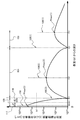
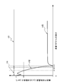
- FIG. 1B is a graph showing one preferred example of the effective semiconductor impurity distribution concentration (C D ) contained in the photovoltaic power generation part of the solar cell shown in FIG. 1A.
- FIG. 1C is a graph showing one preferred example of the effective semiconductor impurity distribution concentration (C D ) contained in the photovoltaic power generation part of the solar cell shown in FIG. 1A.
- FIG. 1A is a schematic configuration explanatory view for explaining the configuration of one example of a preferred embodiment of the solar cell of the present invention.
- FIG. 1B is a graph showing one preferred example of the effective semiconductor impurity distribution concentration (C D ) contained in the photovoltaic power generation part of the solar cell shown in FIG. 1A.
- FIG. 1C is a graph showing one preferred example of the effective semiconductor impurity distribution concentration (C D ) contained in the photovoltaic power generation
- FIG. 1D is a graph showing one preferred example of the effective semiconductor impurity distribution concentration (C D ) contained in the photovoltaic power generation part of the solar cell shown in FIG. 1A.
- FIG. 1E is a graph showing one preferred example of the effective semiconductor impurity distribution concentration (C D ) contained in the photovoltaic power generation part of the solar cell shown in FIG. 1A.
- FIG. 1F is a graph showing one preferred example of the effective semiconductor impurity distribution concentration (C D ) contained in the photovoltaic power generation part of the solar cell shown in FIG. 1A.
- FIG. 1G is a graph showing one preferred example of the effective semiconductor impurity distribution concentration (C D ) contained in the photovoltaic power generation part of the solar cell shown in FIG. 1A.
- FIG. 1E is a graph showing one preferred example of the effective semiconductor impurity distribution concentration (C D ) contained in the photovoltaic power generation part of the solar cell shown in FIG. 1A.
- FIG. 1F is a graph showing
- FIG. 1H is a graph showing one preferred example of the effective semiconductor impurity distribution concentration (C D ) contained in the photovoltaic power generation part of the solar cell shown in FIG. 1A.
- FIG. 1I is a graph showing one preferred example of the effective semiconductor impurity distribution concentration (C D ) contained in the photovoltaic power generation part of the solar cell shown in FIG. 1A.
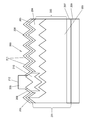
- FIG. 2 is a schematic configuration explanatory view for explaining the configuration of another example of a preferred embodiment of the solar cell of the present invention.
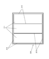
- 2A is a schematic top view of the solar cell shown in FIG.
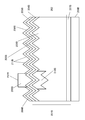
- FIG. 2B is a schematic configuration diagram for explaining the configuration of still another example of a preferred embodiment of the solar cell of the present invention.
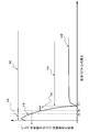
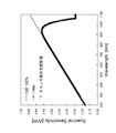
- FIG. 3 is a graph showing an example of the spectral sensitivity characteristic of the embodiment of the present invention.
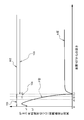
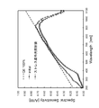
- FIG. 4 is a graph showing an example of the spectral sensitivity characteristic of the comparative example.
- a solar cell 100 shown in FIG. 1A includes a base 101, a photovoltaic power generation unit 100a, an intermediate layer 113, and a passivation layer 114.
- the photovoltaic power generation unit 100 a includes a photovoltaic power generation layer 102 and a UV (ultraviolet ray) deterioration prevention layer 109.
- the photovoltaic generation layer 102 includes a layer region (1) 103 and a layer region (2) 104 made of a semiconductor.
- the layer region (1) 103 and the layer region (2) 104 contain a semiconductor impurity and have a predetermined semiconductor polarity.
- the layer region (2) 104 is an example of a typical example that preferably has a p-type polarity.
- the technical meaning that the layer region is n-type polarity or p-type polarity is that an amount of n-type or p-type semiconductor impurities that contribute to the semiconductor polarity of the layer region (effective semiconductor impurity content) is contained. It means that the layer region has an n-type or p-type semiconductor polarity.
- the UV deterioration preventing layer 109 is composed of a layer region (3) 110 and a layer region (4) 111, and contains a semiconductor impurity and has a predetermined semiconductor polarity.
- the semiconductor impurities contained in the UV deterioration preventing layer 109 are contained in a concentration distribution in the layer thickness direction of the UV deterioration preventing layer 109 (the layer depth direction from the upper surface 107 of the UV deterioration preventing layer 109).
- the concentration distribution in this case is a distribution of semiconductor impurity concentration (hereinafter also referred to as “effective semiconductor impurity concentration”) that contributes to the semiconductor polarity of the UV degradation preventing layer 109 (hereinafter referred to as “effective semiconductor impurity concentration distribution”). Mean).
- the effective semiconductor impurity concentration at the depth (D) from the surface 107 may be referred to as effective semiconductor impurity distribution concentration (C D ).
- the effective semiconductor impurity concentration distribution can be effectively prevented or substantially prevented from degrading the photovoltaic power generation force due to the ultraviolet exposure of the solar cell 100 by making the effective semiconductor impurity concentration distribution as described below.
- the layer region (4) 111 includes a region having a high effective semiconductor impurity concentration (C D ) in the depth direction of the layer, and the maximum value (C D ) of the effective semiconductor impurity distribution concentration (C D ). D Max). That is, as shown in FIG. 1B, the maximum value (C D Max) of the effective semiconductor impurity distribution concentration (C D ) is provided at the maximum value position 108 in the layer region (4) 111.
- the maximum value (C D Max) in the range of the formula (1) UV light is applied to the oxide film (natural oxide film) formed on the surface of the silicon layer inside the solar cell or to the interface between the oxide film and the silicon layer. Even if a fixed charge or an interface state is generated by the irradiation, the electric field lines with the fixed charge can be coupled by carriers or impurity ions in the layer region (4) 111, so that the internal electric field is substantially reduced. It can be made inactive so that the interface state does not become a recombination center. If the maximum value (C D Max) is out of the range of the formula (1), it is difficult to effectively obtain the above effect, which is not preferable.
- the power generation efficiency with respect to the UV light can be improved.
- the maximum value (C D Max) position A0 exceeds 4 nm
- the photoelectric charge photoelectrically converted on the side closer to the silicon surface than the maximum value position is the photovoltaic generation layer. It becomes difficult to reach 102.
- the photocharge generated by irradiation with ultraviolet (UV) light having a short penetration depth in the silicon layer is more likely to disappear due to recombination, so that the photoelectrically converted photocharge is less likely to contribute to the generation of photovoltaic power.
- the power generation efficiency is decreasing.
- the total number of effective impurities contained in the layer region (4) 111 may be larger than the number of fixed charges and interface states generated by UV light irradiation. I can do it.
- the layer thickness (d1) exceeds 20 nm, the internal electric field changes due to the fixed charges and interface states generated by the irradiation of UV light, and the power generation efficiency decreases, which is not preferable.
- the layer thickness (d1 + d2) of the UV deterioration preventing layer 109 is preferably in the following range. 2nm ⁇ (d1 + d2) ⁇ 60nm ⁇ ⁇ ⁇ ⁇ Formula (4)
- the layer thickness (d1 + d2) is less than 2 nm, the total number of effective impurities contained in the layer region (4) is less than the number of fixed charges and interface states generated by UV light irradiation. If the thickness exceeds 60 nm, the internal electric field due to the depletion layer formed by the PN junction is difficult to form near the silicon surface, which makes it difficult to transport the photocharge to the photovoltaic generation layer. .
- electrodes for example, a light receiving surface electrode and a back surface electrode for extracting electric power to the outside are omitted.
- the intermediate layer 113 is formed using an appropriate material and an appropriate manufacturing method and conditions.
- the intermediate layer 112 may be provided for the above purpose, and may be an antireflection film having an antireflection function.
- the surface layer 113 called a covering layer or a sealing layer prevents, for example, reduction of the service life by giving the solar battery 100 water resistance, rainfall resistance, contamination resistance and the like so as not to lower the power generation capacity. It is provided for the purpose.
- FIG. 1B shows one preferred example of the effective distribution concentration of semiconductor impurities (“effective semiconductor impurity distribution concentration (C D )”) contained in the photovoltaic power generation unit 100a.
- the horizontal axis is the depth from the surface 107
- the vertical axis is a logarithmic display of the effective semiconductor impurity distribution concentration (C D ).
- the effective impurity concentration curve of the semiconductor impurity shown in FIG. 1B has three peaks (“Pmax (1), Pmax (2), Pmax (3)”), and each peak can be divided into three regions. I can do it.
- the solar cell 100 clearly shown in FIG.
- an effective semiconductor impurity distribution concentration C D
- Maximum values (peaks) are provided. That is, the maximum value (peak) is at the position of depth D1 in the layer region (1) 103, at the position of depth D2 in the layer region (1) 103, and at the position of depth 108 in the UV degradation preventing layer 109.
- FIG. 1B are the positions (points) B1 (“coordinate display (B1,0)”), C1 (“coordinate display (C1,0) )) Has an inflection point.
- Semiconductor junctions 105 (1) and 105 (2) are formed on the contact surfaces of the layer region (1) 103 and the layer region (2) 104, and the layer region (2) 104 and the UV deterioration preventing layer 109.
- Particularly technically important in the present invention are the shape of the curve of the effective distribution concentration of the semiconductor impurities in the UV degradation preventing layer 109 and the values on the horizontal and vertical axes.
- the peak Pmax (3) (maximum point) in the UV degradation preventing layer 109 is within the layer thickness up to 4 nm in the UV degradation preventing layer 109 with respect to the surface 107, and the value (“peak value”). Or “maximum value”) is preferably at least 1 ⁇ 10 19 pieces / cm 3 .
- the upper limit is preferably 4 ⁇ 10 20 pieces / cm 3 .
- the curve of the effective distribution concentration of the semiconductor impurity on the left side (the “layer region (2) 104” side) from the peak Pmax (3) is steeply reduced.
- the depth position A1 is equal to or less than the depth position (A0) 108 (the “peak Pmax (3)” does not exist in the “layer region (4) 111”) and the effective impurity contained in the layer region (4) 111 Since the total number is smaller than the number of fixed charges and interface states generated by irradiation with UV light, the power generation efficiency is lowered.
- the depth position (A1) is out of the range of the expression (3).
- the layer region 103 is n-type
- the layer region 104 is p-type
- the layer region 109 is n-type.
- the polarity of the n-type and p-type of each layer region can be changed, and this is within the scope of the present invention.
- the density distribution curve peaks at the depth position (D1) 106 (1) and the depth position (D2) 106 (2) from the surface 107, respectively. Pmax (1) and Pmax (2) are provided.
- the effective concentration distribution of the semiconductor impurity in the layer region 103 is substantially the same as that of FIG. 1B, except that it is substantially flat.
- the case of FIG. 1D is substantially the same as the case of FIG. 1C except that the effective concentration distribution of the semiconductor impurity in the layer region (4) 111 is different as shown.
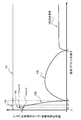
- the effective distribution concentration curve of the semiconductor impurity on the left side in the peak Pmax (3) diagram shows a decreasing trend, but reaches the vertical axis. In the case of FIG. After reaching point Pmin (3), it increases again to point a1 on the vertical axis.
- the distribution concentration value at the point a1 is the same as or larger than the distribution concentration value at the peak Pmax (3).
- FIG. 1E shows another preferred example.
- FIG. 1E is substantially the same as FIG. 1D except that the distribution density curve in the UV degradation preventing layer 109 is different. In the case of FIG. 1E, it decreases once, reaches a minimum point Pmin (3), and then increases again to a point a1 on the vertical axis.
- the distribution concentration value at the point a1 is the same as or larger than the distribution concentration value at the peak Pmax (3).
- FIG. 1F shows another preferred example.
- Curve of the effective semiconductor impurity concentration distribution of the solar cell 100F (C D) shown in Fig. 1F a curve of the effective semiconductor impurity concentration distribution in the case of FIG. 1C (C D), except for the following. That is, the effective semiconductor impurity distribution concentration (C D ) curve of the solar cell shown in FIG. 1F has three inflection points as in FIG. 1C, but the inflection point at position B1 is on the horizontal axis. It is provided at the coordinate point (B1, y1).
- the semiconductor polarities of the layer region (1) 103, the layer region (2) 104, and the UV deterioration preventing layer 109 are n / p / p or p / n / n as shown in the figure.
- FIG. 1G shows yet another preferred example.
- Curve of the effective semiconductor impurity concentration distribution (C D) of the solar cell 100G shown in Fig. 1G the curve of the effective semiconductor impurity concentration distribution in the case of FIG. 1F (C D), except for the following. That is, unlike the case of FIG. 1F, the curve of the effective semiconductor impurity distribution concentration (C D ) of the solar cell shown in FIG. 1G has only one inflection point or substantially only one.
- the curve of the effective semiconductor impurity distribution concentration (C D ) continuously changes.
- the semiconductor polarities of the layer region (2) 104 and the UV deterioration preventing layer 109 are the same polarity. That is, the solar cell shown in FIG. 1G has a semiconductor polar layer structure of n / p / p or p / n / n from the side opposite to the sunlight incident side.
- FIG. 1H shows yet another preferred example.
- the maximum peak Pmax (3) and the minimum peak Pmin (3 ) Is substantially the same as in FIG. 1G.
- FIG. 1I shows yet another preferred example.
- the maximum peak Pmax (3) and the minimum peak Pmin (3) Is substantially the same as in the case of FIG. 1G.
- FIG. 2 shows another preferred embodiment of the present invention.
- FIG. 2 schematically shows the structure of the solar cell 200.
- the layer structure on the light irradiation side has a concavo-convex structure having a saw-like shape, a pyramid shape, or a wave shape.
- the solar cell 200 includes a crystalline semiconductor unit 201.
- the crystalline semiconductor portion 201 is made of a semiconductor material such as a single crystal, polycrystal, or micro / nanocrystalline silicon (Si) semiconductor material, preferably a single crystal silicon (Si) semiconductor material. It is desirable to be done.
- the crystalline semiconductor part 201 has a photovoltaic generation layer 202, a UV deterioration preventing layer 205, and a back surface high concentration layer 207 inside.
- the photovoltaic generation layer 202 has a layer region (1) 203 and a layer region (2) 204.
- a semiconductor junction is formed on the contact surface between the layer region (1) 203 and the layer region (2) 204. This semiconductor junction is formed, for example, by setting one of the layer region (1) 203 and the layer region (2) 204 as a certain semiconductor polarity and the other as a semiconductor polarity different from the polarity.
- one of the layer region (1) 203 and the layer region (2) 204 is P-type and the other is N-type.
- the crystalline semiconductor portion 201 includes an antireflection layer 206 and a light receiving surface electrode 208 on the light irradiation side (upper side in the figure), and a back electrode 209 on the opposite side (lower side in the figure) from the light irradiation side.
- the back surface high-concentration layer 207 is designed to reduce or substantially eliminate the electrical resistance between the layer region (1) 203 and the back surface electrode 209 as much as possible, and to extract the photovoltaic power as efficiently as possible.
- the back surface high concentration layer 207 contains a high concentration of semiconductor impurities having a desired semiconductor polarity.
- the crystalline semiconductor part 201 is made of a Si semiconductor material, it is made of a P + -type or N + -type Si semiconductor material.
- the upper surface high concentration layer 210 provided under the light receiving surface electrode 208 is provided for the same purpose.
- the back electrode 209 is made of, for example, aluminum (Al).
- the UV deterioration preventing layer 205 is not provided below the light-receiving surface electrode 208 that is shielded from light, but may be provided below the light-receiving surface electrode 208 that is shielded from the viewpoint of manufacturing efficiency. Absent.
- the concentration distribution of the semiconductor impurities in the UV deterioration preventing layer 205 any one of the concentration distribution curves shown in FIGS. 1B to 1I is employed.
- FIG. 2A schematically shows the upper surface of the solar cell 200 (the surface seen from the upper side in FIG. 2).
- the light receiving surface electrode 208 is arranged around the solar cell 200 and the entrance surface 211 so that the surface 212 of the light receiving surface electrode 208 is on the light irradiation side as shown in the figure.
- the light receiving surface electrode 208 is made of, for example, silver (Ag).
- FIG. 2B shows another preferred embodiment of the present invention as a modification of the solar cell 200 shown in FIG.
- the solar cell 200B shown in FIG. 2B has a similar layer structure and effective semiconductor impurity distribution concentration (C D ) curve to that of the solar cell shown in FIGS. 1G to 1I.
- the solar cell of the present invention can be formed by ordinary semiconductor manufacturing technology. Therefore, in the explanation of the following steps, the obvious points for engineers in the field are omitted and the main points are simply described.
- Step (1) A Si wafer (semiconductor substrate) is prepared.
- an n-type Si wafer having an n-type impurity concentration of 1 ⁇ 10 14 cm ⁇ 3 is prepared.
- a p-type Si wafer may be used.
- Step (3) Ion implantation for forming a buried p-type semiconductor region is performed.
- the ion implantation conditions are such that the ion species is B + , the implantation energy is 20 keV, and the dose is 4 ⁇ 10 12 cm ⁇ 2 .
- the ion implantation conditions are such that the ion species is BF 2 + , the implantation energy is 8 keV, and the dose is 8.0 ⁇ 10 13 cm ⁇ 2 .
- the wiring interlayer insulating film is etched by wet etching.
- the ion species is BF 2 + , the energy is 35 keV, and the dose is 3.0 ⁇ 10 15 cm ⁇ 2 .
- Step (9) A heat treatment is performed to activate the impurity atoms implanted in the steps (5) and (8). Here, heat treatment at 950 ° C. is performed for 1 second in a nitrogen atmosphere.
- Step (11) In order to form an Al wiring, a part of Al is etched and patterned by dry etching.
- the solar cell of the present invention produced as described above has high sensitivity for the optical wavelength band of 200 to 1100 nm, and particularly has an ideal quantum efficiency for the optical wavelength band of 200 to 900 nm. Furthermore, it has been found that even when intense ultraviolet light using an ultrahigh pressure mercury lamp as a light source is irradiated, the sensitivity does not deteriorate.
- FIG. 3 is a graph showing a typical example of the light receiving sensitivity of the solar cell according to the present invention.
- Samples (1) to (4) were produced by changing only the dose conditions in the step (5).
- the dose is 2.0 ⁇ 10 13 cm ⁇ 2
- sample (2) this example 2
- the dose is 8.0 ⁇ 10 14 cm ⁇ 2
- sample (3) comparative Example 2
- the dose was 1.0 ⁇ 10 13 cm ⁇ 2
- Sample (4) Comparative Example 2
- the dose was 1.6 ⁇ 10 15 cm ⁇ 2 .
- Other process conditions are the same as described above.
- the ion species was BF 2 + , the implantation energy was 25 keV, and the dose was 3.0 ⁇ 10 13 cm ⁇ 2 .
- C D Max was 1 ⁇ 10 19 cm ⁇ 3 and A1 was 25 nm.
- Samples (1) and (2) obtained the same characteristics as in FIG.
- the initial characteristics obtained were the same as those shown in FIG. 3, the sensitivity was greatly deteriorated in the ultraviolet light band after irradiation with ultraviolet light, and no suitable characteristics were obtained.
- sample (4) impurities having a solid solubility or higher were introduced, and as a result, the dark current was high and suitable characteristics could not be obtained.
- sample (5) although the initial characteristics were the same as those shown in FIG. 3, the sensitivity was greatly deteriorated in the ultraviolet light band after irradiation with ultraviolet light, and no suitable characteristics were obtained.
- Step (1A) A Si wafer (semiconductor substrate) is prepared. Here, a p-type Si wafer having a p-type impurity concentration of 1 ⁇ 10 14 cm ⁇ 3 is prepared.
- the ion implantation conditions are such that the ion species is As + , the implantation energy is 35 keV, and the dose is 3 ⁇ 10 15 cm ⁇ 2 .
- FIG. 4 is a graph showing an example of the light receiving sensitivity of the solar cell (comparative sample 4) prepared in the above process. It is below the ideal sensitivity characteristics in the wavelength band of 450nm or less from the initial production stage. This is because there is no internal electric field that efficiently transports the photocharge generated by the light wavelength having a short penetration depth to the photovoltaic generation layer. In addition, the sensitivity in the light wavelength band of 380 nm or less was significantly degraded after irradiation with the ultra-high pressure mercury lamp, and the sensitivity was also degraded from the initial characteristics in the wavelength band of 600 nm or less. As a result, the power generation efficiency of sunlight deteriorated by about 8% compared to the initial value.
Landscapes
- Photovoltaic Devices (AREA)
- Life Sciences & Earth Sciences (AREA)
- Sustainable Development (AREA)
- Chemical & Material Sciences (AREA)
- Crystallography & Structural Chemistry (AREA)
- Engineering & Computer Science (AREA)
- Sustainable Energy (AREA)
Abstract
Description
現在一般的な太陽電池は、P型とN型の半導体を接合した構造(PN接合型太陽電池)を持った、シリコン系、化合物系の太陽電池がある(特許文献1,2)。
本願では、以後において使用される「太陽電池(Solar battery)」の語は、特に断らなければ、単一セル(単一Solar cell)の他、複数セル、セルを複数直並列接続して必要な電圧と電流が得られるようにしたパネル状の製品単体(ソーラーパネルまたはソーラーモジュール、ソーラーアレイといわれている)の何れか若しくは複数を指す意味で使用される。
一方、太陽電池内部に効率よく入射光が吸収されるような試みとして、たとえば、機械
的加工法や反応性イオンエッチング法、結晶面方位に依存しないテクスチャ(微小な凹凸)構造形成法、電気化学反応法や化学エッチング法などで形成した多孔質シリコン構造をテクスチャ構造として利用する方法が提案されている(特許文献1~9)。
上記提案の何れもが、微小凹凸構造によって照射光が多重反射されることで、太陽電池内部に効率よく照射光が吸収されるように試みたものである。
即ち、太陽光には、可視光以外に紫外光(UV光)も含まれているが、このUV光、特に350nm程度以下の光波長のUV光は、エネルギーが高い(約3.5eV超)ので、UV光が太陽電池に照射されると,太陽電池内部のシリコン層表面に形成された酸化膜(自然酸化膜)の中や,酸化膜・シリコン層界面に,固定電荷や界面準位ができる.この固定電荷や界面準位は前記酸化膜中や前記界面に残存(蓄積)するため、UV光の照射履歴とともにそれらの残存量が増加する。
この様に固定電荷や界面準位が増加し続けると,シリコン層の表面下付近において光照射により発生する電子または正孔(シリコン層がP型の場合は電子,N型の場合は正孔)をシリコン層表面に移動させる内部電界が生じてくる.そうなると、光照射により発生する電子または正孔は、形成されている内部電界によりシリコン層表面に移動し,シリコン層表面に蓄積されている電子又は正孔と再結合(光発生電子は蓄積正孔と、光発生正孔は蓄積電子と)して消滅して仕舞うので,光照射により発生する電子または正孔は発電電流に寄与しなくなる。
このため、UV光の照射履歴とともに太陽電池の発電効率の低下が進み何れ実用に耐えない太陽電池になってしまう。このことが、太陽電池の使用寿命を短命にしている。皮肉にも、このUV光の照射による太陽電池の劣化は、赤道など照射光量の多い設置場所になればなる程著しくなり、使用寿命も短命となって投資効率を悪くする。
このようなUV光による劣化を抑制する目的で、紫外線吸収剤等の耐候剤や光安定剤などを含ませた封止材で太陽電池セルを被覆して封止する技術がある。
しかし、この技術は、UV光を有効に利用して発電効率を上げるという視点からは外れるものである上に、太陽電池セルの製造工程数及びコストを増加させる要因となっている。
本願で扱うUV光としては、以下に示される。
紫外線(UV光)は、分類の仕方によって波長領域は多少異なることがあるが、分類される各波長領域の紫外線にはそれぞれ名称が以下の通りにつけられている。
・近紫外線(波長380~200nm)
・UV-A(波長380~315nm)
・UV-B(波長315~280nm)
・UV-C(波長280~200nm)
・遠紫外線(far UV:FUV )又は、真空紫外線(vacuum UV:VU V)(以後統一して遠紫外線という)(波長200~10nm)
・極紫外線若しくは極端紫外線(extreme UV,EUVまたはXUV)(波 長10~1nm) 但し、フォトリソグラフィやレーザー技術においては、遠紫外線(deep UV:DUV)は上記のFUVとは異なり波長300nm以下の紫外線を指 す。
本発明の別の目的は、使用劣化を起こすことなく所期の発電効率を維持できる太陽電池を提供することである。
本発明のもう一つの目的は、UV光耐性に優れとともにUV光を有効に利用して発電効率を向上させることが期待できる太陽電池を提供することである。
n型又はp型のシリコン(Si)半導体基体、
該半導体基体の極性(I)と反対の極性(II)を有し前記半導体基体と半導体接合を形成している半導体層、
該半導体層上に直接設けてあり前記極性(II)と反対の極性(III)を有し、
その層内に含有される該極性(III)の半導体不純物の中、極性(III)に寄与する半導体不純物がその層厚方向に濃度分布し且つその内部に濃度分布の極大値(CDMax)を有するように含有されており、その層厚(d1+d2)が 2~60 nmの範囲にあるUV劣化防止層、
と備え、前記極大値(CDMax)は以下の範囲にあり、
1x10¹⁹個/cm3 ≦ 極大値(CDMax)≦ 4x10²⁰個/cm3 ・・・式(1)
前記極大値(CDMax)の半減値(b1)の位置が前記UV劣化防止層の光入射側の表面からの深さ位置(A1)にあり、その深さ位置(A1)が、
前記極大値(CDMax)の深さ位置(A0)
<(「深さ位置(A1)」)≦ 20nm・・・式(3)
の範囲にあることを特徴とする太陽電池にある。
本発明のもう一つの側面は、
半導体接合を備えている光起電力発生層、
該光起電力発生層上に直接設けてあるUV劣化防止層、
とを、備えており、
前記UV劣化防止層は、その層内に半導体不純物を含有し、該半導体不純物の中、該UV劣化防止層の半導体極性に寄与する半導体不純物がその層厚方向に濃度分布し且つその内部に濃度分布の極大値(CDMax)を有するように含有されており、その層厚(d1+d2)が2~60 nmの範囲にあり、前記極大値(CDMax)は以下の範囲にあり、
1x10¹⁹個/cm3 ≦ 極大値(CDMax)≦ 4x10²⁰個/cm3 ・・・式(1)
前記極大値(CDMax)の半減値(b1)の位置が前記UV劣化防止層の光入射側の表面からの深さ位置(A1)にあり、その深さ位置(A1)が、
前記極大値(CDMax)の深さ位置(A0)
<(「深さ位置(A1)」)≦ 20nm・・・式(3)
の範囲にある事を特徴とする太陽電池にある。
また、別には、UV光耐性に優れとともにUV光を有効に利用して発電効率を向上させることが期待できる太陽電池を提供することもできる。
本発明のその他の特徴及び利点は、添付図面を参照とした以下の説明により明らかになるであろう。なお、添付図面においては、同じ若しくは同様の構成には、同じ参照番号を付す。
光起電力発生部100aは、光起電力発生層102、UV(紫外線)劣化防止層109を備えている。
光起電力発生層102は、半導体で構成される層領域(1)103、層領域(2)104で構成されている。
層領域(1)103、層領域(2)104には、半導体不純物が含有されて所定の半導体極性が付与されている。
例えば、層領域(1)103がn型極性の場合は、層領域(2)104はp型極性とされるのが好適な典型例の一例である。
本願において、層領域がn型極性或いはp型極性ということの技術的意味は、層領域の半導体極性に寄与する量(実効半導体不純物含有量)のn型或いはp型の半導体不純物が含有されて層領域がn型或いはp型の半導体極性が付与されていることをいう。
UV劣化防止層109は、層領域(3)110及び層領域(4)111で構成され、且つ、半導体不純物が含有されて所定の半導体極性が付与されている。UV劣化防止層109中に含有されている半導体不純物は、UV劣化防止層109の層厚方向(UV劣化防止層109の上部表面107からの層深さ方向)に濃度分布して含有されている。この場合の濃度分布は、UV劣化防止層109の半導体極性に寄与する半導体不純物の濃度(以後、「実効半導体不純物濃度」ということもある)の分布(以後、「実効半導体不純物濃度分布」ということもある)を意味する。そして、以後、表面107からの深さ(D)における実効半導体不純物濃度を実効半導体不純物分布濃度(CD)ということもある。
本発明においては、この実効半導体不純物濃度分布を以後の説明のようにすることで太陽電池100の紫外線被爆による光起電力発生力の劣化を効果的に防止若しくは実質的に防止することが出来る。
本発明においては、層領域(4)111は、層の深さ方向に高濃度の実効半導体不純物濃度(CD)の領域を備え、且つ実効半導体不純物分布濃度(CD)の極大値(CDMax)が設けられている。即ち、図1Bに図示するように層領域(4)111内の極大値位置108に、実効半導体不純物分布濃度(CD)の極大値(CDMax)が設けられている。
極大値(CDMax)及び極大値(CDMax)の位置する深さ(Dmax)(=「位置A0の深さ」)の数値範囲は、太陽電池100が紫外線被爆履歴による光起電力発生力の劣化を最大限に防止するのに重要な技術的ファクターである。
本発明において、好ましい極大値(CDMax)及び深さ(Dmax)は、以下の数値範囲にある事が望ましい。
極大値(CDMax)の位置A0(=「深さ(Dmax)」)が、4nmを超えると,極大値の位置よりもシリコン表面に近い側で光電変換した光電荷は光起電力発生層102へ到達しづらくなる。即ち、シリコン層における侵入長が短い紫外(UV)光の照射によって発生する光電荷が再結合によって消滅してしまう確率が高まるため光電変換した光電荷が光起電力の発生に寄与しにくくなるために発電効率の低下傾向が見受けられるようになる。
(「位置(A0)の深さD(A0)」108または「深さ(Dmax)」)
< d1 = (「位置(A1)の深さD(A1)」) ≦ 20nm ・・・・式(3)
『ただし、「位置(A1)の深さD(A1)」とは、実効不純物分布濃度(CD)が、極大値(CDMax)の1/2になる位置の深さと定義される。』
とされるのが好ましい。
層厚(d1)が、20nmを超えると、UV光の照射によって生成される固定電荷および界面準位によって内部電界が変化し,発電効率が低下することとなり好ましくない。
2nm ≦ (d1+d2) ≦ 60nm ・・・・式(4)
尚、図1Aに示す太陽電池100では、外部に電力を取り出すための電極(例えば、受光面電極、裏面電極)は省略されている。
UV劣化防止層109上に更に別の層を設ける場合に、該別の層を直接UV劣化防止層109上に設けると、場合によってはUV劣化防止層109と該別の層との界面若しくは該界面のUV劣化防止層109側付近に表面準位若しくはローカル準位が形成され、発電効率を低下させる原因になる。この点を避けるために中間層113を適切な材料を用いて適切な製法と条件で形成する。
また、中間層112は、上記の目的で設けるほか反射防止機能を持たせて反射防止膜とすることもできる。
被覆層あるいは封止層と呼ばれる表面層113は、例えば、太陽電電池100に耐水性、耐降雨性、耐汚染性などを持たせて発電能力を低下させないようにして耐用年数の低減防止をする目的で設けられる。
以後の図1C~図1Iにおける横軸、縦軸も同様である。
図1Bに示される半導体不純物の実効分布濃度の曲線は、3つのピーク(「Pmax(1)、Pmax(2)、Pmax(3)」)を有し、ピークごとに3つの領域に分けることが出来る。
図1Bに明示す太陽電池100は、層領域(1)103、層領域(2)104、UV劣化防止層109の3領域を備えており、各領域において、実効半導体不純物分布濃度(CD)の極大値(ピーク)が設けられている。即ち、層領域(1)103においては深さD1の位置に、層領域(1)103においては深さD2の位置に、UV劣化防止層109においては深さ108の位置にそれぞれ極大値(ピーク)が設けられた実効半導体不純物分布濃度(CD)を備えた太陽電池100とされている。
図1Bに示す実効半導体不純物分布濃度(CD)の曲線は、位置(点)B1(「座標表示で示せば(B1,0)」),C1(「座標表示で示せば(C1,0)」)において変曲点を有している。
層領域(1)103と層領域(2)104、層領域(2)104とUV劣化防止層109との接触面には、半導体接合105(1)、105(2)がそれぞれ形成されている。
本発明において特に技術的に重要なのは、UV劣化防止層109における半導体不純物の実効分布濃度の曲線の形状と横軸・縦軸の値である。
b1 = 極大値(CDMax)の半減値(個/cm3)・・・式(5)
であることが好ましい。
そのために本発明においては、好ましくは、式(3)を満足するように設計されるのが望ましい。
深さ位置A1が、深さ位置(A0)108以下になる(「ピークPmax(3)」が「層領域(4)111」内に存在しない)と層領域(4)111に含まれる実効不純物総数がUV光の照射によって生成される固定電荷数および界面準位数よりも少なくなることで発電効率が低下してしまうこととなる。20nmを超えると実効半導体不純物分布濃度(CD)の深さ方向の変化によって発生する内部電界が小さくなるため侵入長の短いUV光によって発生する光電荷を光起電力発生層へ輸送しづらくなる。いずれにしても深さ位置(A1)が式(3)に範囲を外れるのは本発明においては好ましくない。
図1Bの例においては、例えば、層領域103がn型であれば、層領域104はp型であり、層領域109はn型である。本発明の場合、各層領域のこのn型、p型を入れ替えた極性にしても差し支えないことは容易に想到でき、本発明の範疇である。
図1Bの例においては、層領域103,104の場合も表面107からの深さ位置(D1)106(1)、深さ位置(D2)106(2)に、それぞれ濃度分布曲線にピ-クPmax(1)、Pmax(2)が設けられている。
図1Dの場合は、層領域(4)111に於ける半導体不純物の実効濃度分布が図示のごとく異なる以外は図1Cの場合と実質的に同じである。
図1B、図1Cの場合は、ピークPmax(3)の図での左側の半導体不純物の実効分布濃度曲線は減少傾向のまま縦軸に至っているが、図1Dの場合は、一旦減少して極小点Pmin(3)に達した後に再び増加して縦軸上にある点a1に至っている。点a1の分布濃度値は、ピークPmax(3)の分布濃度値と同じか若しくは大きな値である。
図1Eは、UV劣化防止層109に於ける分布濃度曲線が異なる以外は、図1Dの場合と実質的に同じである。
図1Eの場合、一旦減少して極小点Pmin(3)に達した後に再び増加して縦軸上にある点a1に至っている。点a1の分布濃度値は、ピークPmax(3)の分布濃度値と同じか若しくは大きな値である。
図1Fに示される太陽電池100Fの実効半導体不純物分布濃度(CD)の曲線は、図1Cの場合の実効半導体不純物分布濃度(CD)の曲線とは、以下の点で異なっている。
即ち、図1Fに示す太陽電池の実効半導体不純物分布濃度(CD)の曲線は、図1Cの場合と同様に3つの変曲点を有するが、位置B1にある変曲点は、横軸上になく、座標点(B1、y1)に設けられている。層領域(1)103、層領域(2)104、UV劣化防止層109の半導体極性は、図示のごとく、n/p/pか若しくはp/n/nである。
図1Gに示される太陽電池100Gの実効半導体不純物分布濃度(CD)の曲線は、図1Fの場合の実効半導体不純物分布濃度(CD)の曲線とは、以下の点で異なっている。
即ち、図1Gに示す太陽電池の実効半導体不純物分布濃度(CD)の曲線は、図1Fの場合と異なり、変曲点一つしか有さないか若しくは実質的に1つしか有さない。
層領域(2)104とUV劣化防止層109との境界では、実効半導体不純物分布濃度(CD)の曲線は、連続的に変化している。そして層領域(2)104とUV劣化防止層109との半導体極性は同極性である。即ち、図1Gに示す太陽電池は、太陽光の入射側と反対側からn/p/pかp/n/nの半導体極性の層構造を有している。
図1Hに示される太陽電池100Hの実効半導体不純物分布濃度(CD)の曲線のUV劣化防止層109の部分において、図1Eの場合の様に、極大ピークPmax(3)と極小ピークPmin(3)を有している以外は、図1Gの場合と実質的に同じである。
図1Iに示される太陽電池100Iの実効半導体不純物分布濃度(CD)の曲線のUV劣化防止層109の部分において、図1Dの場合の様に、極大ピークPmax(3)と極小ピークPmin(3)を有している以外は、図1Gの場合と実質的に同じである。
図2には太陽電池200の構造が模式的に示される。
図2に示す太陽電池100は、光照射側の層構造が鋸状、ピラミット状、或いは波状の凹凸構造を有している。この様な凹凸構造を設けることで多重反射効果により照射光を太陽電池200内に効率よく取り込むことが出来る。
太陽電池200は、結晶性半導体部201を備えている。結晶性半導体部201は、単結晶、多結晶、マイクロ/ナノ結晶の何れかのシリコン(Si)半導体材料などの半導体材料で構成されるが、好ましくは単結晶のシリコン(Si)半導体材料で構成されるのが望ましい。
結晶性半導体部201は、光起電力発生層202とUV劣化防止層205、裏面高濃度層207を内部に有している。
光起電力発生層202は、層領域(1)203と層領域(2)204を有している。層領域(1)203と層領域(2)204との接触面には半導体接合が形成されている。この半導体接合は、例えば、層領域(1)203と層領域(2)204の何れか一方をある半導体極性とし、他方を該極性と異なる半導体極性とすることで形成される。具体的には、層領域(1)203と層領域(2)204の何れか一方をP型とし他方をN型とする。
結晶性半導体部201は、光照射側(図の上側)に、反射防止層206と受光面電極208、光照射側と反対側(図の下側)に裏面電極209を備えている。
裏面高濃度層207は、層領域(1)203と裏面電極209と間の電気的抵抗を可能な限り小さくするか或いは実質的になくし、光起電力の取り出しを可能な限り効率よく行うために設けられる。その目的のために、裏面高濃度層207には、所望の半導体極性の半導体不純物が高濃度に含有される。具体的には、例えば、結晶性半導体部201がSi半導体材料で構成される場合は、P+型又はN+型のSi半導体材料で構成される。
同様な目的で設けられるのが、受光面電極208の下部に設けられる上面高濃度層210である。
裏面電極209は、例えば、アルミニウム(Al)などで構成される。
太陽電池200では、UV劣化防止層205は、遮光される受光面電極208の下部には設けられていないが、製造の効率の点で、遮光される受光面電極208の下部に設けても差し支えない。
UV劣化防止層205中の半導体不純物の濃度分布は、図1B乃至図1Iで示した濃度分布曲線の何れかのパターンが採用される。
受光面電極208は、太陽電池200の周囲と入射面211の周囲に図示のように受光面電極208の表面212が光照射側になるように配されている。受光面電極208は、例えば、銀(Ag)などで構成される。
図2Bに示す太陽電池200Bは、その層構造と実効半導体不純物分布濃度(CD)の曲線が、図1G乃至図1Iに示す太陽電池の場合と類似している。
以下は図1Fに実効濃度分布を示すp+pn型素子構造を有する本発明の太陽電池の主要部の好適な製造例である。
素子構造の極性が逆極性であっても本発明の範疇に入ることは、当該技術分野においては当然のことである。
本発明の太陽電池は、通常の半導体製造技術で形成する事が出来る。従って、以下の工程での説明では当該分野の技術者のとって自明のことは省略し要点を簡略に記載することにする。
Siウェハの不純物濃度は低濃度であるほど長光波長帯域の感度が高くなるため好適であるが、1×1014cm-3以外の不純物濃度を用いても良いことは断るまでもない。また、p型のSiウェハを用いても良い。
・工程(2):半導体基体(n型Siウェハ)表面に7nmのSiO2膜を形成する。ここでは750℃の水分酸化を行うが、化学気相成長法を用いても良い。
また、この工程に先立ち、入射光の反射を抑えるための表面テクスチャ構造を、ウェットエッチング工程等を用いて形成しても良い。
・工程(3):埋め込みp型の半導体領域を形成するためのイオン注入を行う。
イオン注入条件は、イオン種をB+とし、注入エネルギー20keV, ドーズ4×1012cm-2とする。
・工程(4):工程(4)で注入した不純物原子を活性化するために、熱処理を行う。
ここでは、窒素雰囲気において1000℃の熱処理を5秒間行う。
・工程(5):UV劣化阻止層を形成するためのイオン注入を行う。
イオン注入条件は、イオン種をBF2 +とし、注入エネルギー8keV, ドーズ8.0×1013cm-2とする。
・工程(6):配線層間絶縁膜を形成するここでは、化学気相成長法を用いて300nmのSiO2膜を形成する。
・工程(7):埋め込みp型の半導体領域と配線を接続するためのコンタクトホールを開口する。
ここでは、ウェットエッチングによって配線層間絶縁膜をエッチングする。
・工程(8):コンタクトホール開口領域にp+半導体層を形成するためのイオン注入を行う。
ここでは、イオン種をBF2 +とし、エネルギー35keV,ドーズ3.0×1015cm-2とする。
・工程(9):工程(5)および工程(8)で注入した不純物原子を活性化するために、熱処理を行う。ここでは、窒素雰囲気において950℃の熱処理を1秒間行う。
・工程(10):Al配線を形成するために、500nm厚のAl膜を、スパッタ法を用いて成膜する。
・工程(11):Al配線を形成するために、ドライエッチングによってAlの一部の領域をエッチングしパターニングする。
・工程(12):Siウェハ裏面に基体と接続するためのAl電極を形成する。
図3は本発明に係る太陽電池の受光感度の一典型例を示すグラフである
以下に記述する実施例は本発明に関わる典型的な例であるが、本発明を一義的に限定するものではなく、本発明の優位性を示すものである。
前記工程(5)のドーズ条件のみ変化させた試料(1)~(4)を作成した。試料(1)(本例1)では、ドーズを2.0×1013cm-2とし、試料(2)(本例2)では、ドーズを8.0×1014cm-2とし、試料(3)(比較例1)では、ドーズを1.0×1013cm-2とし、試料(4)(比較例2)では、ドーズを1.6×1015cm-2とした。
他の工程の条件は前記したものと同じである。作成した試料のCDMaxは、試料(1)では1×1019cm-3,試料(2)では4×1020cm-3,試料(3)では5×1018cm-3,試料(4)では8×1020cm-3であった。
また、試料(1)~(4)共に、A0は2nm,A1は8nmであり、試料(1)~(4)のいずれも式(3)の条件は満たしていた。試料(1)は式(1)の下限を満たし、試料(2)は式(2)の上限を満たし、試料(3)は式(1)の下限を満たさず、試料(4)は式(1)の上限を満たしていなかった。
更なる比較のために、試料(5)(比較例3)を作成した。試料(5)では前記工程(5)において、イオン種をBF2 +とし、注入エネルギー25keV, ドーズ3.0×1013cm-2とした。
作成した試料(5)においては、CDMaxは1×1019cm-3,A1は25nmであり、式(1)の条件は満たすものの、式(3)の条件は満たしていなかった。
試料(1)および(2)は図3と同等の特性を得た。一方、試料(3)においては、初期特性は図3と同等の特性を得たものの、紫外光を照射した後の紫外光帯域における感度の劣化が大きく、好適な特性が得られなかった。また試料(4)においては、固溶度以上の不純物が導入された結果、暗電流が高く好適な特性が得られなかった。また、試料(5)においては、初期特性は図3と同等の特性を得たものの、紫外光を照射した後の紫外光帯域における感度の劣化が大きく、好適な特性が得られなかった。
・工程(1A):Siウェハ(半導体基体)を準備する。ここではp型の不純物濃度が1×1014cm-3のp型Siウェハを用意する。
・工程(2A):半導体基体(p型Siウェハ)表面を大気中に曝露することで1nm程度の自然酸化膜を形成する。また、この工程に先立ち、入射光の反射を抑えるための表面テクスチャ構造を、ウェットエッチング工程を用いて形成する。
・工程(3A):光起電力発生層の形成のためにp型の半導体基体とpn接合を形成するためn型の半導体領域を形成するためのイオン注入を行う。
イオン注入条件は、イオン種をAs+とし、注入エネルギー35keV, ドーズ3×1015cm-2とする。
・工程(4A):工程(3A)で注入した不純物原子を活性化するために、熱処理を行う。
ここでは、窒素雰囲気において1000℃の熱処理を5秒間行う。
・工程(5A):Al配線を形成するために、500nm厚のAlを、スパッタ法を用いて成膜する。
・工程(6A):Al配線を形成するために、ドライエッチングによってAlの一部の領域をエッチングしパターニングする。
・工程(7A):Siウェハ裏面に基体と接続するためのAl電極を形成する。
100a ・・・・・・光起電力発生部
102,202,202B・・・光起電力発生層
103,203,203B・・・層領域(1)
104,204、204B・・・層領域(2)
105(1),105(2)・・・半導体接合
106(1),106(2)・・・濃度分布曲線のピーク位置
107・・・表面
108・・・極大値位置
109,205,205B・・・・UV劣化防止層
110・・・層領域(3)
111・・・層領域(4)
112・・・中間層
113・・・表面層
201,201B・・・結晶性半導体部
206,206B・・・反射防止膜
207,207B・・・裏面高濃度層
208,208B・・・受光面電極
209,209B・・・裏面電極
210、210B・・・上面高濃度層
211、211B・・入射面
212、212B・・・電極の表面
Claims (2)
- n型又はp型のシリコン(Si)半導体基体、
該半導体基体の極性(I)と反対の極性(II)を有し前記半導体基体と半導体接合を形成している半導体層、
該半導体層上に直接設けてあり前記極性(II)と反対の極性(III)を有し、
その層内に含有される該極性(III)の半導体不純物の中、極性(III)に寄与する半導体不純物がその層厚方向に濃度分布し且つその内部に濃度分布の極大値(CDMax)を有するように含有されており、その層厚(d1+d2)が 2~60 nmの範囲にあるUV劣化防止層、と備え、前記極大値(CDMax)は以下の範囲にあり、
1x10¹⁹個/cm3 ≦ 極大値(CDMax)≦ 4x10²⁰個/cm3 ・・・式(1)
前記極大値(CDMax)の半減値(b1)の位置が前記UV劣化防止層の光入射側の表面からの深さ位置(A1)にあり、その深さ位置(A1)が、
前記極大値(CDMax)の深さ位置(A0)<(「深さ位置(A1)」)≦ 20nm・・・式(3)
の範囲にあることを特徴とする太陽電池。 - 半導体接合を備えている光起電力発生層、
該光起電力発生層上に直接設けてあるUV劣化防止層、
とを、備えており、
前記UV劣化防止層は、その層内に半導体不純物を含有し、該半導体不純物の中、該UV劣化防止層の半導体極性に寄与する半導体不純物がその層厚方向に濃度分布し且つその内部に濃度分布の極大値(CDMax)を有するように含有されており、その層厚(d1+d2)が2~60 nmの範囲にあり、前記極大値(CDMax)は以下の範囲にあり、
1x10¹⁹個/cm3 ≦ 極大値(CDMax)≦ 4x10²⁰個/cm3 ・・・式(1)
前記極大値(CDMax)の半減値(b1)の位置が前記UV劣化防止層の光入射側の表面からの深さ位置(A1)にあり、その深さ位置(A1)が、
前記極大値(CDMax)の深さ位置(A0)<(「深さ位置(A1)」)≦ 20nm・・・式(3)
の範囲にあることを特徴とする太陽電池。
Priority Applications (6)
| Application Number | Priority Date | Filing Date | Title |
|---|---|---|---|
| CN201780088206.6A CN110392936B (zh) | 2017-01-10 | 2017-01-10 | 太阳能电池 |
| KR1020197023293A KR20190100400A (ko) | 2017-01-10 | 2017-01-10 | 태양 전지 |
| PCT/JP2017/000401 WO2018131060A1 (ja) | 2017-01-10 | 2017-01-10 | 太陽電池 |
| US16/476,189 US20200028009A1 (en) | 2017-01-10 | 2017-01-10 | Solar battery |
| JP2018561112A JPWO2018131060A1 (ja) | 2017-01-10 | 2017-01-10 | 太陽電池 |
| TW106101889A TWI706574B (zh) | 2017-01-10 | 2017-01-19 | 太陽電池 |
Applications Claiming Priority (1)
| Application Number | Priority Date | Filing Date | Title |
|---|---|---|---|
| PCT/JP2017/000401 WO2018131060A1 (ja) | 2017-01-10 | 2017-01-10 | 太陽電池 |
Publications (1)
| Publication Number | Publication Date |
|---|---|
| WO2018131060A1 true WO2018131060A1 (ja) | 2018-07-19 |
Family
ID=62840120
Family Applications (1)
| Application Number | Title | Priority Date | Filing Date |
|---|---|---|---|
| PCT/JP2017/000401 Ceased WO2018131060A1 (ja) | 2017-01-10 | 2017-01-10 | 太陽電池 |
Country Status (6)
| Country | Link |
|---|---|
| US (1) | US20200028009A1 (ja) |
| JP (1) | JPWO2018131060A1 (ja) |
| KR (1) | KR20190100400A (ja) |
| CN (1) | CN110392936B (ja) |
| TW (1) | TWI706574B (ja) |
| WO (1) | WO2018131060A1 (ja) |
Citations (2)
| Publication number | Priority date | Publication date | Assignee | Title |
|---|---|---|---|---|
| WO2015151198A1 (ja) * | 2014-03-31 | 2015-10-08 | 国立大学法人東北大学 | 紫外光用固体受光デバイス |
| WO2015170698A1 (ja) * | 2014-05-09 | 2015-11-12 | 国立大学法人東北大学 | 紫外光用固体受光デバイス |
Family Cites Families (12)
| Publication number | Priority date | Publication date | Assignee | Title |
|---|---|---|---|---|
| JP2974485B2 (ja) | 1992-02-05 | 1999-11-10 | キヤノン株式会社 | 光起電力素子の製造法 |
| JPH08204220A (ja) | 1995-01-31 | 1996-08-09 | Mitsubishi Electric Corp | 太陽電池セル、太陽電池モジュール及び太陽電池モジュール群 |
| JPH1078194A (ja) | 1996-09-03 | 1998-03-24 | Fuji Koki Seisakusho:Kk | フレキシブルルーペ |
| JP4903314B2 (ja) | 2001-03-30 | 2012-03-28 | 京セラ株式会社 | 薄膜結晶質Si太陽電池 |
| JP2008005327A (ja) | 2006-06-23 | 2008-01-10 | Toshiba Corp | デジタル放送受信装置を搭載する情報処理装置 |
| JP2012033758A (ja) * | 2010-07-30 | 2012-02-16 | Sharp Corp | 太陽電池 |
| JP2012104733A (ja) | 2010-11-12 | 2012-05-31 | Sony Corp | 光電変換素子および光電変換素子の製造方法 |
| EP2701182A3 (en) * | 2010-12-10 | 2014-06-04 | Teijin Limited | Semiconductor laminate, semiconductor device, method for producing semiconductor laminate, and method for manufacturing semiconductor device |
| JP5868503B2 (ja) | 2012-06-13 | 2016-02-24 | 三菱電機株式会社 | 太陽電池およびその製造方法 |
| JP2014033046A (ja) | 2012-08-02 | 2014-02-20 | Tokuyama Corp | テクスチャー形成用組成物、シリコン基板の製造方法、及びテクスチャー形成用組成物調製キット |
| JP2014229576A (ja) | 2013-05-27 | 2014-12-08 | 凸版印刷株式会社 | 導光板、導光板を備えたバックライトユニットおよび表示装置 |
| CN106024973B (zh) * | 2016-05-31 | 2017-11-24 | 宁夏银星能源光伏发电设备制造有限公司 | 一种抗pid单晶太阳电池镀双层减反射膜工艺 |
-
2017
- 2017-01-10 KR KR1020197023293A patent/KR20190100400A/ko not_active Ceased
- 2017-01-10 WO PCT/JP2017/000401 patent/WO2018131060A1/ja not_active Ceased
- 2017-01-10 US US16/476,189 patent/US20200028009A1/en not_active Abandoned
- 2017-01-10 JP JP2018561112A patent/JPWO2018131060A1/ja active Pending
- 2017-01-10 CN CN201780088206.6A patent/CN110392936B/zh active Active
- 2017-01-19 TW TW106101889A patent/TWI706574B/zh active
Patent Citations (2)
| Publication number | Priority date | Publication date | Assignee | Title |
|---|---|---|---|---|
| WO2015151198A1 (ja) * | 2014-03-31 | 2015-10-08 | 国立大学法人東北大学 | 紫外光用固体受光デバイス |
| WO2015170698A1 (ja) * | 2014-05-09 | 2015-11-12 | 国立大学法人東北大学 | 紫外光用固体受光デバイス |
Also Published As
| Publication number | Publication date |
|---|---|
| JPWO2018131060A1 (ja) | 2019-11-07 |
| US20200028009A1 (en) | 2020-01-23 |
| KR20190100400A (ko) | 2019-08-28 |
| TW201826555A (zh) | 2018-07-16 |
| TWI706574B (zh) | 2020-10-01 |
| CN110392936A (zh) | 2019-10-29 |
| CN110392936B (zh) | 2023-11-24 |
Similar Documents
| Publication | Publication Date | Title |
|---|---|---|
| KR102710224B1 (ko) | 전하-캐리어-선택적 접촉을 통해 연결되는 복수의 흡수체들을 구비한 태양 전지 | |
| TWI559565B (zh) | 具有鏡及光學披覆的垂直柱結構光伏打裝置 | |
| TWI474494B (zh) | 多晶矽發射極太陽能電池所用的圖案化摻雜 | |
| US8603900B2 (en) | Reducing surface recombination and enhancing light trapping in solar cells | |
| KR101740523B1 (ko) | 태양 전지 및 그 제조 방법 | |
| US20160284896A1 (en) | Solar cell emitter region fabrication with differentiated p-type and n-type architectures and incorporating a multi-purpose passivation and contact layer | |
| US20020011263A1 (en) | Multi-junction solar cell | |
| EP3161874B1 (en) | Passivation of light-receiving surfaces of solar cells with crystalline silicon | |
| US20120000506A1 (en) | Photovoltaic module and method of manufacturing the same | |
| TWI460867B (zh) | 光伏裝置和製造其之方法 | |
| GB2034973A (en) | Solar cell with multi-layer insulation | |
| US20120138129A1 (en) | Bifacial solar cell | |
| JP2023041057A (ja) | 太陽電池およびその製造方法、光起電力モジュール | |
| Sánchez et al. | A Laser‐Processed Silicon Solar Cell with Photovoltaic Efficiency in the Infrared | |
| US20130048070A1 (en) | Tunnel photovoltaic | |
| US20130125964A1 (en) | Solar cell and manufacturing method thereof | |
| JP2024006933A (ja) | 光起電力セル及びその製造方法、光起電力モジュール | |
| JPH08330611A (ja) | シリコン太陽電池セルとその製造方法 | |
| US20130276872A1 (en) | Solar cell unit and method for manufacturing the same | |
| EP3998643A1 (en) | Semiconductor device and solar battery and production method for semiconductor device | |
| TWI706574B (zh) | 太陽電池 | |
| US20230027354A1 (en) | Doped semiconductor structure for nir sensors | |
| KR101711440B1 (ko) | 다결정실리콘 광검출기의 제조방법 | |
| JP2016039246A (ja) | 光電変換素子 | |
| US20120048358A1 (en) | Solar cell and method for manufacturing the same |
Legal Events
| Date | Code | Title | Description |
|---|---|---|---|
| 121 | Ep: the epo has been informed by wipo that ep was designated in this application |
Ref document number: 17891436 Country of ref document: EP Kind code of ref document: A1 |
|
| ENP | Entry into the national phase |
Ref document number: 2018561112 Country of ref document: JP Kind code of ref document: A |
|
| NENP | Non-entry into the national phase |
Ref country code: DE |
|
| ENP | Entry into the national phase |
Ref document number: 20197023293 Country of ref document: KR Kind code of ref document: A |
|
| 122 | Ep: pct application non-entry in european phase |
Ref document number: 17891436 Country of ref document: EP Kind code of ref document: A1 |