WO2018095437A1 - Pilotage distributif de panneau d'affichage à cristaux liquides (lcd) - Google Patents
Pilotage distributif de panneau d'affichage à cristaux liquides (lcd) Download PDFInfo
- Publication number
- WO2018095437A1 WO2018095437A1 PCT/CN2017/113352 CN2017113352W WO2018095437A1 WO 2018095437 A1 WO2018095437 A1 WO 2018095437A1 CN 2017113352 W CN2017113352 W CN 2017113352W WO 2018095437 A1 WO2018095437 A1 WO 2018095437A1
- Authority
- WO
- WIPO (PCT)
- Prior art keywords
- pixels
- lines
- source
- gate
- subpixels
- Prior art date
Links
Images


Classifications
-
- G—PHYSICS
- G09—EDUCATION; CRYPTOGRAPHY; DISPLAY; ADVERTISING; SEALS
- G09G—ARRANGEMENTS OR CIRCUITS FOR CONTROL OF INDICATING DEVICES USING STATIC MEANS TO PRESENT VARIABLE INFORMATION
- G09G3/00—Control arrangements or circuits, of interest only in connection with visual indicators other than cathode-ray tubes
- G09G3/20—Control arrangements or circuits, of interest only in connection with visual indicators other than cathode-ray tubes for presentation of an assembly of a number of characters, e.g. a page, by composing the assembly by combination of individual elements arranged in a matrix no fixed position being assigned to or needed to be assigned to the individual characters or partial characters
- G09G3/2092—Details of a display terminals using a flat panel, the details relating to the control arrangement of the display terminal and to the interfaces thereto
- G09G3/2096—Details of the interface to the display terminal specific for a flat panel
-
- G—PHYSICS
- G09—EDUCATION; CRYPTOGRAPHY; DISPLAY; ADVERTISING; SEALS
- G09G—ARRANGEMENTS OR CIRCUITS FOR CONTROL OF INDICATING DEVICES USING STATIC MEANS TO PRESENT VARIABLE INFORMATION
- G09G3/00—Control arrangements or circuits, of interest only in connection with visual indicators other than cathode-ray tubes
- G09G3/20—Control arrangements or circuits, of interest only in connection with visual indicators other than cathode-ray tubes for presentation of an assembly of a number of characters, e.g. a page, by composing the assembly by combination of individual elements arranged in a matrix no fixed position being assigned to or needed to be assigned to the individual characters or partial characters
- G09G3/22—Control arrangements or circuits, of interest only in connection with visual indicators other than cathode-ray tubes for presentation of an assembly of a number of characters, e.g. a page, by composing the assembly by combination of individual elements arranged in a matrix no fixed position being assigned to or needed to be assigned to the individual characters or partial characters using controlled light sources
- G09G3/30—Control arrangements or circuits, of interest only in connection with visual indicators other than cathode-ray tubes for presentation of an assembly of a number of characters, e.g. a page, by composing the assembly by combination of individual elements arranged in a matrix no fixed position being assigned to or needed to be assigned to the individual characters or partial characters using controlled light sources using electroluminescent panels
- G09G3/32—Control arrangements or circuits, of interest only in connection with visual indicators other than cathode-ray tubes for presentation of an assembly of a number of characters, e.g. a page, by composing the assembly by combination of individual elements arranged in a matrix no fixed position being assigned to or needed to be assigned to the individual characters or partial characters using controlled light sources using electroluminescent panels semiconductive, e.g. using light-emitting diodes [LED]
- G09G3/3208—Control arrangements or circuits, of interest only in connection with visual indicators other than cathode-ray tubes for presentation of an assembly of a number of characters, e.g. a page, by composing the assembly by combination of individual elements arranged in a matrix no fixed position being assigned to or needed to be assigned to the individual characters or partial characters using controlled light sources using electroluminescent panels semiconductive, e.g. using light-emitting diodes [LED] organic, e.g. using organic light-emitting diodes [OLED]
- G09G3/3225—Control arrangements or circuits, of interest only in connection with visual indicators other than cathode-ray tubes for presentation of an assembly of a number of characters, e.g. a page, by composing the assembly by combination of individual elements arranged in a matrix no fixed position being assigned to or needed to be assigned to the individual characters or partial characters using controlled light sources using electroluminescent panels semiconductive, e.g. using light-emitting diodes [LED] organic, e.g. using organic light-emitting diodes [OLED] using an active matrix
-
- G—PHYSICS
- G02—OPTICS
- G02F—OPTICAL DEVICES OR ARRANGEMENTS FOR THE CONTROL OF LIGHT BY MODIFICATION OF THE OPTICAL PROPERTIES OF THE MEDIA OF THE ELEMENTS INVOLVED THEREIN; NON-LINEAR OPTICS; FREQUENCY-CHANGING OF LIGHT; OPTICAL LOGIC ELEMENTS; OPTICAL ANALOGUE/DIGITAL CONVERTERS
- G02F1/00—Devices or arrangements for the control of the intensity, colour, phase, polarisation or direction of light arriving from an independent light source, e.g. switching, gating or modulating; Non-linear optics
- G02F1/01—Devices or arrangements for the control of the intensity, colour, phase, polarisation or direction of light arriving from an independent light source, e.g. switching, gating or modulating; Non-linear optics for the control of the intensity, phase, polarisation or colour
- G02F1/13—Devices or arrangements for the control of the intensity, colour, phase, polarisation or direction of light arriving from an independent light source, e.g. switching, gating or modulating; Non-linear optics for the control of the intensity, phase, polarisation or colour based on liquid crystals, e.g. single liquid crystal display cells
- G02F1/133—Constructional arrangements; Operation of liquid crystal cells; Circuit arrangements
- G02F1/1333—Constructional arrangements; Manufacturing methods
- G02F1/1335—Structural association of cells with optical devices, e.g. polarisers or reflectors
- G02F1/133509—Filters, e.g. light shielding masks
- G02F1/133514—Colour filters
-
- G—PHYSICS
- G02—OPTICS
- G02F—OPTICAL DEVICES OR ARRANGEMENTS FOR THE CONTROL OF LIGHT BY MODIFICATION OF THE OPTICAL PROPERTIES OF THE MEDIA OF THE ELEMENTS INVOLVED THEREIN; NON-LINEAR OPTICS; FREQUENCY-CHANGING OF LIGHT; OPTICAL LOGIC ELEMENTS; OPTICAL ANALOGUE/DIGITAL CONVERTERS
- G02F1/00—Devices or arrangements for the control of the intensity, colour, phase, polarisation or direction of light arriving from an independent light source, e.g. switching, gating or modulating; Non-linear optics
- G02F1/01—Devices or arrangements for the control of the intensity, colour, phase, polarisation or direction of light arriving from an independent light source, e.g. switching, gating or modulating; Non-linear optics for the control of the intensity, phase, polarisation or colour
- G02F1/13—Devices or arrangements for the control of the intensity, colour, phase, polarisation or direction of light arriving from an independent light source, e.g. switching, gating or modulating; Non-linear optics for the control of the intensity, phase, polarisation or colour based on liquid crystals, e.g. single liquid crystal display cells
- G02F1/133—Constructional arrangements; Operation of liquid crystal cells; Circuit arrangements
- G02F1/136—Liquid crystal cells structurally associated with a semi-conducting layer or substrate, e.g. cells forming part of an integrated circuit
- G02F1/1362—Active matrix addressed cells
- G02F1/136286—Wiring, e.g. gate line, drain line
-
- G—PHYSICS
- G02—OPTICS
- G02F—OPTICAL DEVICES OR ARRANGEMENTS FOR THE CONTROL OF LIGHT BY MODIFICATION OF THE OPTICAL PROPERTIES OF THE MEDIA OF THE ELEMENTS INVOLVED THEREIN; NON-LINEAR OPTICS; FREQUENCY-CHANGING OF LIGHT; OPTICAL LOGIC ELEMENTS; OPTICAL ANALOGUE/DIGITAL CONVERTERS
- G02F1/00—Devices or arrangements for the control of the intensity, colour, phase, polarisation or direction of light arriving from an independent light source, e.g. switching, gating or modulating; Non-linear optics
- G02F1/01—Devices or arrangements for the control of the intensity, colour, phase, polarisation or direction of light arriving from an independent light source, e.g. switching, gating or modulating; Non-linear optics for the control of the intensity, phase, polarisation or colour
- G02F1/13—Devices or arrangements for the control of the intensity, colour, phase, polarisation or direction of light arriving from an independent light source, e.g. switching, gating or modulating; Non-linear optics for the control of the intensity, phase, polarisation or colour based on liquid crystals, e.g. single liquid crystal display cells
- G02F1/133—Constructional arrangements; Operation of liquid crystal cells; Circuit arrangements
- G02F1/136—Liquid crystal cells structurally associated with a semi-conducting layer or substrate, e.g. cells forming part of an integrated circuit
- G02F1/1362—Active matrix addressed cells
- G02F1/1368—Active matrix addressed cells in which the switching element is a three-electrode device
-
- G—PHYSICS
- G09—EDUCATION; CRYPTOGRAPHY; DISPLAY; ADVERTISING; SEALS
- G09G—ARRANGEMENTS OR CIRCUITS FOR CONTROL OF INDICATING DEVICES USING STATIC MEANS TO PRESENT VARIABLE INFORMATION
- G09G3/00—Control arrangements or circuits, of interest only in connection with visual indicators other than cathode-ray tubes
- G09G3/20—Control arrangements or circuits, of interest only in connection with visual indicators other than cathode-ray tubes for presentation of an assembly of a number of characters, e.g. a page, by composing the assembly by combination of individual elements arranged in a matrix no fixed position being assigned to or needed to be assigned to the individual characters or partial characters
- G09G3/2007—Display of intermediate tones
- G09G3/2074—Display of intermediate tones using sub-pixels
-
- G—PHYSICS
- G09—EDUCATION; CRYPTOGRAPHY; DISPLAY; ADVERTISING; SEALS
- G09G—ARRANGEMENTS OR CIRCUITS FOR CONTROL OF INDICATING DEVICES USING STATIC MEANS TO PRESENT VARIABLE INFORMATION
- G09G3/00—Control arrangements or circuits, of interest only in connection with visual indicators other than cathode-ray tubes
- G09G3/20—Control arrangements or circuits, of interest only in connection with visual indicators other than cathode-ray tubes for presentation of an assembly of a number of characters, e.g. a page, by composing the assembly by combination of individual elements arranged in a matrix no fixed position being assigned to or needed to be assigned to the individual characters or partial characters
- G09G3/22—Control arrangements or circuits, of interest only in connection with visual indicators other than cathode-ray tubes for presentation of an assembly of a number of characters, e.g. a page, by composing the assembly by combination of individual elements arranged in a matrix no fixed position being assigned to or needed to be assigned to the individual characters or partial characters using controlled light sources
- G09G3/30—Control arrangements or circuits, of interest only in connection with visual indicators other than cathode-ray tubes for presentation of an assembly of a number of characters, e.g. a page, by composing the assembly by combination of individual elements arranged in a matrix no fixed position being assigned to or needed to be assigned to the individual characters or partial characters using controlled light sources using electroluminescent panels
- G09G3/32—Control arrangements or circuits, of interest only in connection with visual indicators other than cathode-ray tubes for presentation of an assembly of a number of characters, e.g. a page, by composing the assembly by combination of individual elements arranged in a matrix no fixed position being assigned to or needed to be assigned to the individual characters or partial characters using controlled light sources using electroluminescent panels semiconductive, e.g. using light-emitting diodes [LED]
- G09G3/3208—Control arrangements or circuits, of interest only in connection with visual indicators other than cathode-ray tubes for presentation of an assembly of a number of characters, e.g. a page, by composing the assembly by combination of individual elements arranged in a matrix no fixed position being assigned to or needed to be assigned to the individual characters or partial characters using controlled light sources using electroluminescent panels semiconductive, e.g. using light-emitting diodes [LED] organic, e.g. using organic light-emitting diodes [OLED]
- G09G3/3266—Details of drivers for scan electrodes
-
- G—PHYSICS
- G09—EDUCATION; CRYPTOGRAPHY; DISPLAY; ADVERTISING; SEALS
- G09G—ARRANGEMENTS OR CIRCUITS FOR CONTROL OF INDICATING DEVICES USING STATIC MEANS TO PRESENT VARIABLE INFORMATION
- G09G3/00—Control arrangements or circuits, of interest only in connection with visual indicators other than cathode-ray tubes
- G09G3/20—Control arrangements or circuits, of interest only in connection with visual indicators other than cathode-ray tubes for presentation of an assembly of a number of characters, e.g. a page, by composing the assembly by combination of individual elements arranged in a matrix no fixed position being assigned to or needed to be assigned to the individual characters or partial characters
- G09G3/22—Control arrangements or circuits, of interest only in connection with visual indicators other than cathode-ray tubes for presentation of an assembly of a number of characters, e.g. a page, by composing the assembly by combination of individual elements arranged in a matrix no fixed position being assigned to or needed to be assigned to the individual characters or partial characters using controlled light sources
- G09G3/30—Control arrangements or circuits, of interest only in connection with visual indicators other than cathode-ray tubes for presentation of an assembly of a number of characters, e.g. a page, by composing the assembly by combination of individual elements arranged in a matrix no fixed position being assigned to or needed to be assigned to the individual characters or partial characters using controlled light sources using electroluminescent panels
- G09G3/32—Control arrangements or circuits, of interest only in connection with visual indicators other than cathode-ray tubes for presentation of an assembly of a number of characters, e.g. a page, by composing the assembly by combination of individual elements arranged in a matrix no fixed position being assigned to or needed to be assigned to the individual characters or partial characters using controlled light sources using electroluminescent panels semiconductive, e.g. using light-emitting diodes [LED]
- G09G3/3208—Control arrangements or circuits, of interest only in connection with visual indicators other than cathode-ray tubes for presentation of an assembly of a number of characters, e.g. a page, by composing the assembly by combination of individual elements arranged in a matrix no fixed position being assigned to or needed to be assigned to the individual characters or partial characters using controlled light sources using electroluminescent panels semiconductive, e.g. using light-emitting diodes [LED] organic, e.g. using organic light-emitting diodes [OLED]
- G09G3/3275—Details of drivers for data electrodes
-
- G—PHYSICS
- G09—EDUCATION; CRYPTOGRAPHY; DISPLAY; ADVERTISING; SEALS
- G09G—ARRANGEMENTS OR CIRCUITS FOR CONTROL OF INDICATING DEVICES USING STATIC MEANS TO PRESENT VARIABLE INFORMATION
- G09G3/00—Control arrangements or circuits, of interest only in connection with visual indicators other than cathode-ray tubes
- G09G3/20—Control arrangements or circuits, of interest only in connection with visual indicators other than cathode-ray tubes for presentation of an assembly of a number of characters, e.g. a page, by composing the assembly by combination of individual elements arranged in a matrix no fixed position being assigned to or needed to be assigned to the individual characters or partial characters
- G09G3/34—Control arrangements or circuits, of interest only in connection with visual indicators other than cathode-ray tubes for presentation of an assembly of a number of characters, e.g. a page, by composing the assembly by combination of individual elements arranged in a matrix no fixed position being assigned to or needed to be assigned to the individual characters or partial characters by control of light from an independent source
- G09G3/36—Control arrangements or circuits, of interest only in connection with visual indicators other than cathode-ray tubes for presentation of an assembly of a number of characters, e.g. a page, by composing the assembly by combination of individual elements arranged in a matrix no fixed position being assigned to or needed to be assigned to the individual characters or partial characters by control of light from an independent source using liquid crystals
- G09G3/3607—Control arrangements or circuits, of interest only in connection with visual indicators other than cathode-ray tubes for presentation of an assembly of a number of characters, e.g. a page, by composing the assembly by combination of individual elements arranged in a matrix no fixed position being assigned to or needed to be assigned to the individual characters or partial characters by control of light from an independent source using liquid crystals for displaying colours or for displaying grey scales with a specific pixel layout, e.g. using sub-pixels
-
- G—PHYSICS
- G09—EDUCATION; CRYPTOGRAPHY; DISPLAY; ADVERTISING; SEALS
- G09G—ARRANGEMENTS OR CIRCUITS FOR CONTROL OF INDICATING DEVICES USING STATIC MEANS TO PRESENT VARIABLE INFORMATION
- G09G3/00—Control arrangements or circuits, of interest only in connection with visual indicators other than cathode-ray tubes
- G09G3/20—Control arrangements or circuits, of interest only in connection with visual indicators other than cathode-ray tubes for presentation of an assembly of a number of characters, e.g. a page, by composing the assembly by combination of individual elements arranged in a matrix no fixed position being assigned to or needed to be assigned to the individual characters or partial characters
- G09G3/34—Control arrangements or circuits, of interest only in connection with visual indicators other than cathode-ray tubes for presentation of an assembly of a number of characters, e.g. a page, by composing the assembly by combination of individual elements arranged in a matrix no fixed position being assigned to or needed to be assigned to the individual characters or partial characters by control of light from an independent source
- G09G3/36—Control arrangements or circuits, of interest only in connection with visual indicators other than cathode-ray tubes for presentation of an assembly of a number of characters, e.g. a page, by composing the assembly by combination of individual elements arranged in a matrix no fixed position being assigned to or needed to be assigned to the individual characters or partial characters by control of light from an independent source using liquid crystals
- G09G3/3611—Control of matrices with row and column drivers
- G09G3/3648—Control of matrices with row and column drivers using an active matrix
- G09G3/3666—Control of matrices with row and column drivers using an active matrix with the matrix divided into sections
-
- G—PHYSICS
- G09—EDUCATION; CRYPTOGRAPHY; DISPLAY; ADVERTISING; SEALS
- G09G—ARRANGEMENTS OR CIRCUITS FOR CONTROL OF INDICATING DEVICES USING STATIC MEANS TO PRESENT VARIABLE INFORMATION
- G09G3/00—Control arrangements or circuits, of interest only in connection with visual indicators other than cathode-ray tubes
- G09G3/20—Control arrangements or circuits, of interest only in connection with visual indicators other than cathode-ray tubes for presentation of an assembly of a number of characters, e.g. a page, by composing the assembly by combination of individual elements arranged in a matrix no fixed position being assigned to or needed to be assigned to the individual characters or partial characters
- G09G3/34—Control arrangements or circuits, of interest only in connection with visual indicators other than cathode-ray tubes for presentation of an assembly of a number of characters, e.g. a page, by composing the assembly by combination of individual elements arranged in a matrix no fixed position being assigned to or needed to be assigned to the individual characters or partial characters by control of light from an independent source
- G09G3/36—Control arrangements or circuits, of interest only in connection with visual indicators other than cathode-ray tubes for presentation of an assembly of a number of characters, e.g. a page, by composing the assembly by combination of individual elements arranged in a matrix no fixed position being assigned to or needed to be assigned to the individual characters or partial characters by control of light from an independent source using liquid crystals
- G09G3/3611—Control of matrices with row and column drivers
- G09G3/3674—Details of drivers for scan electrodes
- G09G3/3677—Details of drivers for scan electrodes suitable for active matrices only
-
- G—PHYSICS
- G09—EDUCATION; CRYPTOGRAPHY; DISPLAY; ADVERTISING; SEALS
- G09G—ARRANGEMENTS OR CIRCUITS FOR CONTROL OF INDICATING DEVICES USING STATIC MEANS TO PRESENT VARIABLE INFORMATION
- G09G3/00—Control arrangements or circuits, of interest only in connection with visual indicators other than cathode-ray tubes
- G09G3/20—Control arrangements or circuits, of interest only in connection with visual indicators other than cathode-ray tubes for presentation of an assembly of a number of characters, e.g. a page, by composing the assembly by combination of individual elements arranged in a matrix no fixed position being assigned to or needed to be assigned to the individual characters or partial characters
- G09G3/34—Control arrangements or circuits, of interest only in connection with visual indicators other than cathode-ray tubes for presentation of an assembly of a number of characters, e.g. a page, by composing the assembly by combination of individual elements arranged in a matrix no fixed position being assigned to or needed to be assigned to the individual characters or partial characters by control of light from an independent source
- G09G3/36—Control arrangements or circuits, of interest only in connection with visual indicators other than cathode-ray tubes for presentation of an assembly of a number of characters, e.g. a page, by composing the assembly by combination of individual elements arranged in a matrix no fixed position being assigned to or needed to be assigned to the individual characters or partial characters by control of light from an independent source using liquid crystals
- G09G3/3611—Control of matrices with row and column drivers
- G09G3/3685—Details of drivers for data electrodes
- G09G3/3688—Details of drivers for data electrodes suitable for active matrices only
-
- G—PHYSICS
- G09—EDUCATION; CRYPTOGRAPHY; DISPLAY; ADVERTISING; SEALS
- G09G—ARRANGEMENTS OR CIRCUITS FOR CONTROL OF INDICATING DEVICES USING STATIC MEANS TO PRESENT VARIABLE INFORMATION
- G09G2300/00—Aspects of the constitution of display devices
- G09G2300/04—Structural and physical details of display devices
- G09G2300/0421—Structural details of the set of electrodes
- G09G2300/0426—Layout of electrodes and connections
-
- G—PHYSICS
- G09—EDUCATION; CRYPTOGRAPHY; DISPLAY; ADVERTISING; SEALS
- G09G—ARRANGEMENTS OR CIRCUITS FOR CONTROL OF INDICATING DEVICES USING STATIC MEANS TO PRESENT VARIABLE INFORMATION
- G09G2300/00—Aspects of the constitution of display devices
- G09G2300/04—Structural and physical details of display devices
- G09G2300/0439—Pixel structures
- G09G2300/0465—Improved aperture ratio, e.g. by size reduction of the pixel circuit, e.g. for improving the pixel density or the maximum displayable luminance or brightness
-
- G—PHYSICS
- G09—EDUCATION; CRYPTOGRAPHY; DISPLAY; ADVERTISING; SEALS
- G09G—ARRANGEMENTS OR CIRCUITS FOR CONTROL OF INDICATING DEVICES USING STATIC MEANS TO PRESENT VARIABLE INFORMATION
- G09G2300/00—Aspects of the constitution of display devices
- G09G2300/08—Active matrix structure, i.e. with use of active elements, inclusive of non-linear two terminal elements, in the pixels together with light emitting or modulating elements
- G09G2300/0804—Sub-multiplexed active matrix panel, i.e. wherein one active driving circuit is used at pixel level for multiple image producing elements
-
- G—PHYSICS
- G09—EDUCATION; CRYPTOGRAPHY; DISPLAY; ADVERTISING; SEALS
- G09G—ARRANGEMENTS OR CIRCUITS FOR CONTROL OF INDICATING DEVICES USING STATIC MEANS TO PRESENT VARIABLE INFORMATION
- G09G2300/00—Aspects of the constitution of display devices
- G09G2300/08—Active matrix structure, i.e. with use of active elements, inclusive of non-linear two terminal elements, in the pixels together with light emitting or modulating elements
- G09G2300/0809—Several active elements per pixel in active matrix panels
- G09G2300/0814—Several active elements per pixel in active matrix panels used for selection purposes, e.g. logical AND for partial update
-
- G—PHYSICS
- G09—EDUCATION; CRYPTOGRAPHY; DISPLAY; ADVERTISING; SEALS
- G09G—ARRANGEMENTS OR CIRCUITS FOR CONTROL OF INDICATING DEVICES USING STATIC MEANS TO PRESENT VARIABLE INFORMATION
- G09G2310/00—Command of the display device
- G09G2310/02—Addressing, scanning or driving the display screen or processing steps related thereto
- G09G2310/0202—Addressing of scan or signal lines
- G09G2310/0205—Simultaneous scanning of several lines in flat panels
- G09G2310/021—Double addressing, i.e. scanning two or more lines, e.g. lines 2 and 3; 4 and 5, at a time in a first field, followed by scanning two or more lines in another combination, e.g. lines 1 and 2; 3 and 4, in a second field
-
- G—PHYSICS
- G09—EDUCATION; CRYPTOGRAPHY; DISPLAY; ADVERTISING; SEALS
- G09G—ARRANGEMENTS OR CIRCUITS FOR CONTROL OF INDICATING DEVICES USING STATIC MEANS TO PRESENT VARIABLE INFORMATION
- G09G2310/00—Command of the display device
- G09G2310/02—Addressing, scanning or driving the display screen or processing steps related thereto
- G09G2310/0243—Details of the generation of driving signals
-
- G—PHYSICS
- G09—EDUCATION; CRYPTOGRAPHY; DISPLAY; ADVERTISING; SEALS
- G09G—ARRANGEMENTS OR CIRCUITS FOR CONTROL OF INDICATING DEVICES USING STATIC MEANS TO PRESENT VARIABLE INFORMATION
- G09G2310/00—Command of the display device
- G09G2310/02—Addressing, scanning or driving the display screen or processing steps related thereto
- G09G2310/0262—The addressing of the pixel, in a display other than an active matrix LCD, involving the control of two or more scan electrodes or two or more data electrodes, e.g. pixel voltage dependent on signals of two data electrodes
-
- G—PHYSICS
- G09—EDUCATION; CRYPTOGRAPHY; DISPLAY; ADVERTISING; SEALS
- G09G—ARRANGEMENTS OR CIRCUITS FOR CONTROL OF INDICATING DEVICES USING STATIC MEANS TO PRESENT VARIABLE INFORMATION
- G09G2310/00—Command of the display device
- G09G2310/02—Addressing, scanning or driving the display screen or processing steps related thereto
- G09G2310/0264—Details of driving circuits
- G09G2310/0297—Special arrangements with multiplexing or demultiplexing of display data in the drivers for data electrodes, in a pre-processing circuitry delivering display data to said drivers or in the matrix panel, e.g. multiplexing plural data signals to one D/A converter or demultiplexing the D/A converter output to multiple columns
-
- G—PHYSICS
- G09—EDUCATION; CRYPTOGRAPHY; DISPLAY; ADVERTISING; SEALS
- G09G—ARRANGEMENTS OR CIRCUITS FOR CONTROL OF INDICATING DEVICES USING STATIC MEANS TO PRESENT VARIABLE INFORMATION
- G09G2380/00—Specific applications
- G09G2380/02—Flexible displays
Definitions
- the disclosure relates generally to display technologies, and more particularly, to driving of display panel.
- Display resolution is limited by the physical size of a display panel in each of the width dimension (i.e., in the row/horizontal direction) and the height dimension (i.e., in the column/vertical direction) , as well as the minimum pattern size of fabricating the components on the display panel in each dimension.
- known display systems can have a very large number of source lines (a.k.a. data lines) arranged in the row direction, which can increase the manufacturing complexity and cost.
- a wide quad high-definition (WQHD) display panel e.g., resolution is 1440 ⁇ 2560
- the real-RGB subpixel arrangement the ratio is 3
- the number of the source lines may be 4320.
- aperture ratio is one of the important characteristics because it affects the brightness and power consumption of the displays.
- the total area occupied by the gate and source lines in each subpixel region has greater impact on the aperture ratio of LCDs.
- the disclosure relates generally to display technologies, and more particularly, to driving of display panel.
- a liquid crystal display (LCD) apparatus includes a color filter layer, a liquid crystal (LC) layer, and a pixel circuit layer.
- the color filter layer includes a plurality of color filters corresponding to an array of pixels arranged in M rows and N columns. The number of the color filters is k times of the number of the pixels.
- the LC layer is divided into a plurality of LC regions, each of which corresponds to a respective one of the color filters.
- the pixel circuit layer includes a plurality pixel circuits, each of which is configured to drive a respective one of the LC regions.
- the pixel circuit layer also includes xM gate lines and (k/x) N source lines, where x is a fraction larger than 1, and each of xM and (k/x) N is a positive integer.
- an LCD apparatus in another example, includes a color filter layer, an LC layer, a pixel circuit layer, a gate driving circuit, a source driving circuit, and control logic.
- the color filter layer includes a plurality of color filters corresponding to an array of pixels arranged in M rows and N columns. The number of the color filters is k times of the number of the pixels.
- the LC layer is divided into a plurality of LC regions, each of which corresponds to a respective one of the color filters.
- the pixel circuit layer includes a plurality pixel circuits, each of which is configured to drive a respective one of the LC regions.
- the pixel circuit layer includes xM gate lines and (k/x) N source lines, where x is a fraction larger than 1, and each of xM and (k/x) N is a positive integer.
- the gate driving circuit is operatively coupled to the pixel circuit layer via the xM gate lines and configured to scan the plurality of pixel circuits.
- the source driving circuit is operatively coupled to the pixel circuit layer via the (k/x) N source lines and configured to write display data in a frame to the plurality of pixel circuits.
- the control logic is operatively coupled to the gate driving circuit and source driving circuit and configured to receive original display data and convert the original display data into converted display data based on the (k/x) N source lines.
- the control logic is also configured to provide a first set of control signals to the gate driving circuit to control the gate driving circuit to scan the plurality of pixel circuits via the xM gate lines.
- the control logic is further configured to provide a second set of control signals to the source driving circuit to control the source driving circuit to write the converted display data to the plurality of pixel circuits.
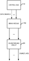
- FIG. 1 is a block diagram illustrating an apparatus including a display and control logic in accordance with an embodiment
- FIGs. 2A and 2B are block diagrams illustrating the display shown in FIG. 1 including drivers in accordance with an embodiment
- FIG. 3 is a depiction of an arrangement of gate lines and source lines for driving a display panel having an array of pixels
- FIG. 4 is a block diagram illustrating one example of the control logic shown in FIG. 1 in accordance with an embodiment
- FIG. 5A is a depiction of an arrangement of gate lines and source lines for driving of subpixels in an example arrangement
- FIG. 5B is a depiction of an arrangement of gate lines and source lines for distributive-driving of subpixels in the example arrangement shown in FIG. 5A in accordance with an embodiment
- FIG. 5C is a depiction of another arrangement of gate lines and source lines for distributive-driving of subpixels in the example arrangement shown in FIG. 5A in accordance with an embodiment
- FIG. 5D is a depiction of still another arrangement of gate lines and source lines for distributive-driving of subpixels in the example arrangement shown in FIG. 5A in accordance with an embodiment
- FIG. 6A is a depiction of an arrangement of gate lines and source lines for driving of subpixels in another example arrangement
- FIG. 6B is a depiction of an arrangement of gate lines and source lines for distributive-driving of subpixels in the example arrangement shown in FIG. 6A in accordance with an embodiment
- FIG. 6C is a depiction of another arrangement of gate lines and source lines for distributive-driving of subpixels in the example arrangement shown in FIG. 6A in accordance with an embodiment
- FIG. 6D is a depiction of still another arrangement of gate lines and source lines for distributive-driving of subpixels in the example arrangement shown in FIG. 6A in accordance with an embodiment
- FIG. 7A is a depiction of an arrangement of gate lines and source lines for driving of subpixels in still another example arrangement
- FIG. 7B is a depiction of an arrangement of gate lines and source lines for distributive-driving of subpixels in the example arrangement shown in FIG. 7A in accordance with an embodiment
- FIG. 7C is a depiction of another arrangement of gate lines and source lines for distributive-driving of subpixels in the example arrangement shown in FIG. 7A in accordance with an embodiment
- FIG. 7D is a depiction of still another arrangement of gate lines and source lines for distributive-driving of subpixels in the example arrangement shown in FIG. 7A in accordance with an embodiment
- FIG. 8A is a depiction of an arrangement of gate lines and source lines for driving of subpixels in yet another example arrangement
- FIG. 8B is a depiction of an arrangement of gate lines and source lines for distributive-driving of subpixels in the example arrangement shown in FIG. 8A in accordance with an embodiment
- FIG. 8C is a depiction of another arrangement of gate lines and source lines for distributive-driving of subpixels in the example arrangement shown in FIG. 8A in accordance with an embodiment
- FIG. 9A is a depiction of an arrangement of gate lines and source lines for driving of subpixels in yet another example arrangement
- FIG. 9B is a depiction of an arrangement of gate lines and source lines for distributive-driving of subpixels in the example arrangement shown in FIG. 9A in accordance with an embodiment
- FIG. 9C is a depiction of another arrangement of gate lines and source lines for distributive-driving of subpixels in the example arrangement shown in FIG. 9A in accordance with an embodiment
- FIG. 10 is a block diagram illustrating a demultiplexing module operatively coupled to the control logic and source driver shown in FIG. 2A in accordance with an embodiment
- FIG. 11 is a block diagram illustrating one example of the demultiplexing module shown in FIG. 10 in accordance with an embodiment
- FIG. 12A is a depiction of an arrangement of gate lines and source lines for distributive-driving with source-demultiplexing of subpixels in the example arrangement shown in FIG. 5A in accordance with an embodiment
- FIG. 12B is a depiction of another arrangement of gate lines and source lines for distributive-driving with source-demultiplexing of subpixels in the example arrangement shown in FIG. 5A in accordance with an embodiment
- FIGs. 13A-13D are depictions of an arrangement of gate lines and source lines for distributive-driving with source-demultiplexing of subpixels in the example arrangement shown in FIG. 6A in accordance with an embodiment
- FIG. 14 is a cross-sectional view illustrating one example of an LCD apparatus in accordance with an embodiment
- FIG. 15A is a circuit diagram illustrating one example of a pixel circuit of an LCD apparatus in accordance with an embodiment
- FIG. 15B is a layout diagram illustrating one example of a subpixel of an LCD apparatus in accordance with an embodiment
- FIG. 16A is a depiction of an arrangement of gate lines and source lines for driving subpixels in an example arrangement of an LCD apparatus
- FIG. 16B is a depiction of an arrangement of gate lines and source lines for distributive-driving of subpixels in an example arrangement of an LCD apparatus in accordance with an embodiment
- FIGs. 17A-17B are depictions of example color filter arrangements for distributive-driving of subpixels of an LCD apparatus in accordance with various embodiments
- FIGs. 18A-18C are depictions of arrangements of gate lines, source lines, and pixel circuits for distributive-driving of subpixels in the example arrangement shown in FIG. 16B in accordance with an embodiment
- FIG. 19A is a depiction of a color filter arrangement of an LCD apparatus.
- FIG. 19B is a depiction of an example color filter arrangement for distributive-driving of subpixels of an LCD apparatus in accordance with an embodiment.
- terms, such as “a, ” “an, ” or “the, ” again, may be understood to convey a singular usage or to convey a plural usage, depending at least in part upon context.
- the term “based on” may be understood as not necessarily intended to convey an exclusive set of factors and may, instead, allow for existence of additional factors not necessarily expressly described, again, depending at least in part on context.
- the distributive-driving of display panel disclosed herein can reduce the number of source lines or gate lines.
- the timing specification of display panels can be optimized.
- the reduction of source lines may be achieved by distributing the driving load to the source and gate lines according to an optimal ratio based on the specific subpixel arrangement of the display panel.
- the distributive-driving of display panel disclosed herein may not overburden the gate scan (e.g., by doubling the number of gate lines) and thus, would not significantly reduce the scan period of each subpixel.
- the reduction of gate lines may be achieved by distributing the driving load to the source and gate lines according to an optimal ratio based on the specific subpixel arrangement of the display panel.
- the reduction of gate lines, as well as the corresponding driving circuits, can help to achieve the narrow-bezel or bezel-less designs.
- the scan period of each subpixel can be increased because of the less gate lines to be scanned in each frame.
- source-demultiplexing can be combined with the distributive-driving so that the number of data channels (a.k.a. source channels) provided by control logic, e.g., driver integrated circuit (IC) , does not need to increase to the same number of the source lines, thereby avoiding increasing the design and manufacturing complexity and cost.
- control logic e.g., driver integrated circuit (IC)
- the extra wiring caused by the distributive-driving may not reduce the aperture ratio of display because each subpixel is a top emitting OLED.
- AMOLED active-matrix organic light-emitting diode
- the single-layer COF package can be used for flexible displays, such as for packaging driver ICs of flexible displays with high resolution, thereby reducing the manufacturing cost compared with the traditional flexible displays using multi-layer COF package.
- FIG. 1 illustrates an apparatus 100 including a display 102 and control logic 104.
- Apparatus 100 may be any suitable device, for example, a virtual reality (VR) or augmented reality (AR) device (e.g., VR headset, etc. ) , handheld device (e.g., dumb or smart phone, tablet, etc. ) , wearable device (e.g., eyeglasses, wrist watch, etc. ) , automobile control station, gaming console, television set, laptop computer, desktop computer, netbook computer, media center, set-top box, global positioning system (GPS) , electronic billboard, electronic sign, printer, or any other suitable device.
- VR virtual reality
- AR augmented reality
- handheld device e.g., dumb or smart phone, tablet, etc.
- wearable device e.g., eyeglasses, wrist watch, etc.
- gaming console television set, laptop computer, desktop computer, netbook computer, media center, set-top box, global positioning system (GPS) , electronic billboard, electronic sign,
- display 102 is operatively coupled to control logic 104 and is part of apparatus 100, such as but not limited to, a head-mounted display, handheld device screen, computer monitor, television screen, head-up display (HUD) , dashboard, electronic billboard, or electronic sign.
- Display 102 may be an OLED display, liquid crystal display (LCD) , E-ink display, electroluminescent display (ELD) , billboard display with LED or incandescent lamps, or any other suitable type of display.
- Control logic 104 may be any suitable hardware, software, firmware, or combination thereof, configured to receive display data 106 (e.g., pixel data) and generate control signals 108 for driving the subpixels on display 102.
- Control signals 108 are used for controlling writing of display data 106 (either in its original form or in a converted form) to the subpixels and directing operations of display 102.
- SPR subpixel rendering
- control logic 104 in one embodiment may include a control signal generating module 402 having a timing controller (TCON) 408 and a clock generator 410, a data interface 404, and a data converting module 406 having a storing unit 412 and a data reconstructing unit 414 .
- Control logic 104 may include any other suitable components, such as an encoder, a decoder, one or more processors, controllers, and storage devices.
- Control logic 104 may be implemented as a standalone IC chip, such as an application-specific integrated circuit (ASIC) or a field-programmable gate array (FPGA) .
- ASIC application-specific integrated circuit
- FPGA field-programmable gate array
- Apparatus 100 may also include any other suitable components such as, but not limited to tracking devices 110 (e.g., inertial sensors, camera, eye tracker, GPS, or any other suitable devices for tracking motion of eyeballs, facial expression, head movement, body movement, and hand and body gesture) , input devices 112 (e.g., a mouse, keyboard, remote controller, handwriting device, microphone, scanner, etc. ) , and speakers (not shown) .
- tracking devices 110 e.g., inertial sensors, camera, eye tracker, GPS, or any other suitable devices for tracking motion of eyeballs, facial expression, head movement, body movement, and hand and body gesture
- input devices 112 e.g., a mouse, keyboard, remote controller, handwriting device, microphone, scanner, etc.
- speakers not shown
- control logic 104 may be manufactured in a chip-on-glass (COG) package, for example, when display 102 is a rigid display.
- control logic 104 may be manufactured in a COF package, for example, when display 102 is a flexible display, e.g., a flexible OLED display.
- COG chip-on-glass
- control logic 104 may be manufactured in a COF package, for example, when display 102 is a flexible display, e.g., a flexible OLED display.
- the distribute-driving of display panel can optimize the numbers of source lines and gate lines.
- control logic 104 may be manufactured in a single-layer COF package due to the less number of source lines.
- control logic 104 may be integrated with drivers, such as gate drivers, source drivers, and light emitting drivers, in a driver IC.
- the driver IC including control logic 104 and drivers, may be manufactured in a COF package, such as a single-layer COF package.
- apparatus 100 may be a handheld or a VR/AR device, such as a smart phone, a tablet, or a VR headset.
- Apparatus 100 may also include a processor 114 and memory 116.
- Processor 114 may be, for example, a graphics processor (e.g., graphics processing unit (GPU) ) , an application processor (AP) , a general processor (e.g., APU, accelerated processing unit; GPGPU, general-purpose computing on GPU) , or any other suitable processor.
- Memory 116 may be, for example, a discrete frame buffer or a unified memory.
- Processor 114 is configured to generate display data 106 in display frames and may temporally store display data 106 in memory 116 before sending it to control logic 104.
- Processor 114 may also generate other data, such as but not limited to, control instructions 118 or test signals, and provide them to control logic 104 directly or through memory 116. Control logic 104 then receives display data 106 from memory 116 or from processor
- FIGs. 2A and 2B are block diagrams illustrating display 102 shown in FIG. 1 including drivers in accordance with an embodiment.
- Display 102 in this embodiment includes a display panel having an active region 200 including a plurality of subpixels 201.
- the display panel may also include on-panel drivers, e.g., a gate driver 202 and a source driver 204.
- gate driver 202 and source driver 204 may not be on-panel drivers, i.e., not parts of the display panel, but instead are operatively coupled to the display panel.
- Each subpixel 201 may be any of the units that make up a pixel, i.e., a subdivision of a pixel.
- a subpixel 201 may be a single-color display element that can be individually addressed.
- each subpixel 201 may include an OLED, such as a top emitting OLED, and a pixel circuit for driving the OLED.
- Each OLED can emit a light in a predetermined brightness and color, such as but not limited to, red, green, blue, yellow, cyan, magenta, or white.
- Each pixel circuit includes thin film transistors (TFTs) and is configured to drive the corresponding subpixel 201 by controlling the light emitting from the respective OLED according to control signals 108 from control logic 104.
- the pixel circuit may be in a 2T1C configuration (i.e., including a switching transistor, a driving transistor, and a storage capacitor) or may include a compensation circuit with more transistors and/or capacitors for brightness uniformity, such as in a 7T1C, 5T1C, 5T2C, or 6T1C configuration.
- each subpixel 201 may include a color filter, a liquid crystal region, and a pixel circuit for driving the liquid crystal region.
- a subpixel 201 may present a distinct color and brightness, such as but not limited to, red, green, blue, yellow, cyan, magenta, or white.
- Each pixel circuit includes at least one TFT (e.g., a switching transistor) and a storage capacitor.
- the plurality of subpixels correspond to an array of pixels arranged in M rows and N columns.
- the number of the subpixels may be k times of the number of the pixels. That is, k subpixels may constitute one pixel, and each pixel may consist of k subpixels. k may be any positive integer larger than 1. In some embodiments, k may be 2, 3, or 4.
- each row of pixels may include N pixels arranged in the row/horizontal direction (but are not necessarily in a straight line) , which include kN subpixels.
- each column of pixels may include M pixels arranged in the column/vertical direction (but are not necessarily in a straight line) , which include M subpixels.
- the k subpixels of each pixel may not be physically aligned.
- the centers of the k subpixels of each pixel may not be in a straight line in the row/horizontal direction and/or in a straight line in the column/vertical direction.
- the colors, sizes, and/or shapes of the k subpixels of each pixel may not be the same as well.
- display 102 (and the display panel thereof) has a resolution of N ⁇ M, which corresponds to the array of pixels arranged in the M rows and N columns. That is, display 102 can be characterized by its display resolution, which is the number of distinct pixels in each dimension that can be displayed. For example, for a WQHD display with a resolution of 1440 ⁇ 2560, the corresponding array of pixels is arranged in 2560 rows and 1440 columns.
- display data 106 is provided by processor 114 in display frames. For each frame, display data 106 includes M ⁇ N pieces of pixel data, and each piece of pixel data corresponds to one pixel of the array of pixels.
- Each pixel may be considered as a sample of an original image represented by a piece of pixel data having multiple components, such as multiple color components or a luminance and multiple chrominance components.
- each piece of pixel data includes a first component representing a first color, a second component representing a second color, and a third component representing a third color.
- the first, second, and third colors may be three primary colors (i.e., red, green, and blue) so that each pixel can present a full color. That is, display data 106 may be programmed at the pixel-level.
- three subpixels may constitute one pixel, i.e., k is 3.
- each of the three components of a piece of pixel data may be used to render one of the three subpixels of the respective pixel.
- four subpixels may constitute one pixel, i.e., k is 4.
- one of the four subpixels of a pixel (e.g., a white subpixel) may be rendered based on at least one of the three components of the respective piece of pixel data.
- U.S. Patent No. 9,165,526 having a title of “Subpixel Arrangement of Displays and Methods for Rendering the Same, ” which is incorporated herein by reference.
- two subpixels may constitute one pixel, i.e., k is 2.
- SPR algorithms may be used to render the two subpixels of each pixel based on the specific subpixel arrangement. Examples are disclosed in U.S. Patent No. 8,786,645, having a title of “Subpixel Arrangement of Displays and Methods for Rendering the Same, ” U.S. Patent No. 9,418,586, having a title of “Subpixel Arrangement of Displays and Methods for Rendering the Same, ” U.S. Patent Application Publication No. 2015/0339969, having a title of “Method and Apparatus for Subpixel Rendering, ” U.S. Patent Application Publication No.
- Gate driver 202 in this embodiment is operatively coupled to active region 200 via a plurality of gate lines (a.k.a. scan lines) and configured to scan the plurality of subpixels 201 based on at least some of control signals 108.
- gate driver 202 applies a plurality of scan signals, which are generated based on control signals 108 from control logic 104, to the plurality of gate lines for scanning the plurality of subpixels 201 in a gate scanning order.
- a scan signal is applied to the gate electrode of a switching transistor of each pixel circuit during the scan period to turn on the switching transistor so that the data signal for the corresponding subpixel 201 can be written by source driver 204.
- source driver 204 It is to be appreciated that although one gate driver 202 is illustrated in FIG. 2A, in some embodiments, multiple gate drivers may work in conjunction with each other to scan the subpixels 201.
- M gate lines are provided for an array of pixels (PX) arranged in M rows and N columns.
- Subpixels in each of the M rows of pixels are operatively coupled to one gate line and are scanned by a scan signal transmitted via the gate line.
- the number of the gate lines is the same as the number of the rows of pixels (M) .
- subpixels in each of the M rows of pixels are operatively coupled to two gate lines and are scanned by two scan signals transmitted via the two gate lines. That is, the number of the gate lines is twice of the number of the rows of pixels (i.e., dual-gate driving) . For example, one half of the subpixels in a row of pixels may be scanned via one gate line, and the other half of the subpixels in the same row of pixels may be scanned via another gate line.
- the number of the gate lines is xM, wherein x is a faction between 1 and 2.
- x is a faction between 1 and 2.
- subpixels in each of the M rows of pixels are operatively coupled to more than one but less than two gate lines and are scanned by scan signals transmitted via the gate lines.
- the number of the gate lines is larger than the number of the rows of pixels, but less than twice of the number of the rows of pixels.
- x may be represented as p/q, wherein each of p and q is a positive integer, and p is larger than q and is smaller than 2q.
- x may be 3/2, 4/3, 5/3, 5/4, 7/4, 6/5, 7/5, 8/5, 9/5, 7/6, 11/6, 8/7, 9/7, 10/7, 11/7, 12/7, 13/7, 9/8, 11/8, 13/8, 15/8, 10/9, 11/9, 13/9, 14/9, 16/9, or 17/9, to name a few. It is to be appreciated that x is not limited to the examples given above and may be any faction between 1 and 2.
- the value of x may be determined based on the specific subpixel arrangement to balance the driving load between the gate and source lines (e.g., the numbers of gate and source lines) and/or to simplify the wiring of gate lines and/or source lines on the display panel. It is to be appreciated that in this embodiment, the number of gate/scan channels provided by control logic 104 may be the same as or different from the number of gate lines, e.g., smaller than M due to demultiplexing.
- the number of the gate lines is xM, wherein x is a faction between 0 and 1.
- x is a faction between 0 and 1.
- subpixels in each of the M rows of pixels are operatively coupled to less than one gate line, and subpixels in more than one row of pixels are scanned by scan signal transmitted via one gate line.
- the number of the gate lines is smaller than the number of the rows of pixels.
- x may be represented as p/q, wherein each of p and q is a positive integer, and q is larger than p.
- p may be equal to 1.
- subpixels in every q rows of pixels are operatively coupled to one gate line.
- p may be larger than 1.
- subpixels in every q rows of pixels are operatively coupled to p gate lines.
- the value of x may be determined based on the specific subpixel arrangement to balance the driving load between the gate and source lines (e.g., the numbers of gate and source lines) and/or to simplify the wiring of gate lines and/or source lines on the display panel. Consequently, compared with the example shown in FIG. 3, the number of gate lines (and the corresponding driving circuits, e.g., in gate driver 202) can be reduced by a factor of (1-x) so that the scan period of each subpixel can be increased in each frame.
- the reduction of gate lines and corresponding driving circuits can also help the narrow-bezel or bezel-less designs of the display panel. It is to be appreciated that in this embodiment, the number of gate/scan channels in control logic 104 may be the same as or different from the number of gate lines, e.g., smaller than M due to demultiplexing.
- Source driver 204 in this embodiment is operatively coupled to active region 200 via a plurality of source lines (a.k.a. data lines) and configured to write display data 106 in a frame to the plurality of subpixels 201 based on at least some of control signals 108.
- source driver 204 may simultaneously apply a plurality of data signals to the plurality of source lines for the subpixels 201.
- source driver 204 may include one or more shift registers, digital-analog converters (DAC) , multiplexers (MUX) , and arithmetic circuit for controlling a timing of application of voltage to the source electrode of the switching transistor of each pixel circuit (i.e., during the scan period in each frame) and a magnitude of the applied voltage according to gradations of display data 106. It is to be appreciated that although one source driver 204 is illustrated in FIG. 2A, in some embodiments, multiple source drivers may work in conjunction with each other to apply the data signals to the source lines for the subpixels 201.
- the number of subpixels are k times of the number of pixels.
- the subpixels may be represented as M ⁇ N ⁇ k.
- the k subpixels constituting one pixel are operatively coupled to the same gate line, and the subpixels may be represented as M ⁇ kN.
- kN source lines S1, ...Sk, S (k+1) , ...S2k, ..., S (nk-1) , ..., Skn
- k source lines are provided for each pixel.
- Subpixels in each of the N columns of pixels are operatively coupled to k source lines and are written with k data signals transmitted via the k source lines.
- the number of the source lines is k times of the number of the columns of pixels (N) .
- the source lines may be operatively coupled to the columns of subpixels in a “zigzag” manner.
- the number of the source lines may be more than k times of the number of the columns of pixels (N) .
- the number of the source lines may be kN+1.
- the k subpixels constituting one pixel are operatively coupled to two gate lines, and the subpixels may be represented as 2M ⁇ (k/2) N.
- subpixels in each of the N columns of pixels are operatively coupled to k/2 source lines and are written with data signals transmitted via the k/2 source lines. That is, the number of the gate lines is k/2 times of the number of the columns of pixels (N) .
- the number of the source lines is yN, where y is k/x.
- the subpixels are represented as xM ⁇ (k/x) N.
- xM and (k/x) N is a positive integer.
- subpixels in each of the N columns of pixels are operatively coupled to k/x source lines and are written with data signals transmitted via the k/x source lines.
- the number of the source lines ( (k/x) N) is smaller than the number of the columns of pixels multiplied by the ratio k of the subpixels to the pixels (kN) , but is larger than one half of the number of the columns of pixels multiplied by the ratio k ( (k/2) N) . Consequently, compared with the example shown in FIG. 3, the number of source lines can be reduced by a factor of (1-1/x) so that the manufacturing complexity and cost may be reduced. It is to be appreciated that the number of source/data channels in control logic 104 may be the same as or different from the number of source lines due to demultiplexing.
- the number of the source lines is yN, where y is k/x.
- the subpixels are represented as xM ⁇ (k/x) N.
- Each of xM and (k/x) N is a positive integer.
- subpixels in each of the N columns of pixels are operatively coupled to k/x source lines and are written with data signals transmitted via the k/x source lines. Because x is between 0 and 1 in this embodiment, the number of the source lines ( (k/x) N) is larger than the number of the columns of pixels multiplied by the ratio k of the subpixels to the pixels (kN) .
- the number of source/data channels provided by control logic 104 may be different from the number of source lines due to demultiplexing. That is, the number of data channels may maintain the same by the source-demultiplexing even the number of source lines increases due to the distributive-driving.
- the number of the gate lines may be xM, and the number of the source lines may be (k/x) N, wherein x is a faction between 0 and 2, and each of xM and (k/x) N is a positive integer.
- x may be represented as p/q, wherein each of p and q is a positive integer, and p is smaller than 2q and does not equal to q.
- the value of x i.e., p and q
- the number of gate lines and/or source lines may be more than xM and (k/x) N, respectively due to the “zigzag” connection of gate lines or source lines.
- the number of source lines may be (k/x) N+1 or (k/x) N+2 when the source lines are operatively coupled to the columns of subpixels in a “zigzag” manner.
- a light emitting driver 206 may be included on the display panel in some embodiments in which display 102 is an OLED display. Light emitting driver 206 may be operatively coupled to active region 200 and configured to cause each subpixel to emit light in each frame. It is to be appreciated that although one light emitting driver 206 is illustrated in FIG. 2A, in some embodiments, multiple light emitting drivers may work in conjunction with each other.
- FIG. 4 is a block diagram illustrating one example of control logic 104 shown in FIG. 1 in accordance with an embodiment.
- control logic 104 is an IC (but may alternatively include a state machine made of discrete logic and other components) , which provides an interface function between processor 114/memory 116 and display 102.
- Control logic 104 may provide various control signals 108 with suitable voltage, current, timing, and de-multiplexing, to cause display 102 to show the desired text or image.
- Control logic 104 may be an application-specific microcontroller and may include storage units such as RAM, flash memory, EEPROM, and/or ROM, which may store, for example, firmware and display fonts.
- control logic 104 includes control signal generating module 402, data interface 404, and data converting module 406.
- Data interface 404 may be any display data interface, such as but not limited to, display serial interface (DSI) , display pixel interface (DPI) , and display bus interface (DBI) by the Mobile Industry Processor Interface (MIPI) Alliance, unified display interface (UDI) , digital visual interface (DVI) , high-definition multimedia interface (HDMI) , and DisplayPort (DP) .
- Data interface 404 is configured to receive display data 106 in multiple frames and any other control instructions 118 or test signals. Display data 106 may be received in consecutive frames at any frame rates, such as 30, 60, 72, 120, or 240 frames per second (fps) . The received display data 106 is forwarded by data interface 404 to control signal generating module 402 and data converting module 406.
- control signal generating module 402 provides control signals 108 to gate driver 202 and source driver 204 (optionally to light emitting driver 206) to drive the subpixels in active region 200.
- Control signal generating module 402 may include TCON 408 and clock generator 410.
- TCON 408 may provide a variety of enable signals to gate driver 202 and source driver 204 (optionally to light emitting driver 206) , respectively.
- Clock generator 410 may provide a variety of clock signals to gate driver 202 and source driver 204 (optionally to light emitting driver 206) , respectively.
- display data 106 may be programmed at the pixel-level. In each frame, display data 106 may include M ⁇ N pieces of pixel data corresponding to the array of pixels arranged in the M rows and N columns. Because of the distributive-driving of display panel disclosed herein, the number of the source lines is no longer the same as the number of the columns of pixels multiplied by the ratio k (kN) , i.e., the number of data channels (kN) , but instead becomes (k/x) N. Thus, in some embodiments, display data 106 may be converted into converted display data 416 to accommodate the source line and gate line arrangement due to the specific distributive-driving scheme. In this embodiment, data converting module 406 provides converted display data 416 to source driver 204 based on the source line and gate line arrangement on the display panel. In some embodiments, the timing of each data signal may be re-arranged according to the gate scanning order as well.
- data converting module 406 in this embodiment includes storing unit 412 and data reconstructing unit 414.
- Storing unit 412 is configured to receive display data 106 (original display data) and store display data 106 in each frame because the conversion of display data 106 may be performed at the frame-level.
- Storing unit 412 may be data latches or line buffers that temporally store display data 106 forwarded by data interface 404.
- Data reconstructing unit 414 is operatively coupled to storing unit 412 and configured to reconstruct, in each frame, display data 106 into corresponding converted display data 416 based on the source line and gate line arrangement on the display panel.
- Data reconstructing unit 414 of data converting module 406 may convert display data 106 into converted display data 416 based on the number of source lines ( (k/x) N) according to the distributive-driving scheme. For example, any suitable sampling algorithms may be used by data reconstructing unit 414 to obtain converted display data 416 suitable for the (k/x) N source lines. It is to be appreciated that in some embodiments, data converting module 406 may not be included in control logic 104. Instead, processor 114 may adjust the timing of display data 106 to accommodate the source line and gate line arrangement on the display panel.
- FIG. 5A is a depiction of an arrangement of gate lines and source lines for driving of subpixels in an example arrangement.
- the display panel includes an array of subpixels in a first color A, a second color B, and a third color C, arranged in rows and columns.
- A, B, and C denote three different colors, such as but not limited to, red, green, blue, yellow, cyan, magenta, or white. It is to be appreciated that the “array, ” “row, ” and “column” of subpixels may not correspond to the “array, ” “row, ” and “column” of pixels described above.
- Subpixels A, B, and C are alternatively arranged in every three adjacent rows of the array of subpixels.
- a first subpixel in one of the A, B, and C colors and a second subpixel in the same color as the first subpixel may be by 3 units in the row/horizontal direction and 4 units in the column/vertical direction.
- the first and second subpixels may have a minimum distance among subpixels in the same color.
- FIG. 5A illustrates a portion of the display panel including 24 subpixels.
- the array of pixels in this example is arranged in two rows and is operatively coupled to two gate lines G1 and G2.
- the array of pixels may be arranged in four columns, each of which is operatively coupled to three source lines, or arranged in six columns, each of which is operatively coupled to two source lines.
- the array of pixels in this example is operatively coupled to 12 source lines S1 to S12.
- the number of the gate lines (2) is the same as the number of the rows of pixels (2)
- the number of the source lines (12) is the same as the number of the columns of pixels multiplied by the ratio k (4 ⁇ 3 or 6 ⁇ 2) .
- FIG. 5B is a depiction of an arrangement of gate lines and source lines for distributive-driving of subpixels in the example arrangement shown in FIG. 5A in accordance with an embodiment.
- the display panel with the same subpixel arrangement illustrated in FIG. 5A is driven by a distributive-driving scheme to reduce the number of source lines.
- the array of pixels is operatively coupled to three gate lines G1-G3, which is one and a half (3/2) times of the number of the rows of pixels (2) .
- the scan period of each subpixel is reduced to two thirds (2/3) of the scan period of each subpixel in the example shown in FIG. 5A, which is greater than the scan period of the example using the dual-gate driving (i.e., one half (1/2) of the scan period of each subpixel in the example shown in FIG. 5A) .
- the gate lines shown in FIGs. 5A and 5B represent the logical connections between subpixels. The actual wiring of the gate lines may be understood by a person of ordinary skill in the art based on the logical connections and may be different in different examples.
- the array of pixels is operatively coupled to eight source lines S1-S8, which is two thirds (2/3) of the number of the columns of pixels multiplied by the ratio k (12) .
- the number of the source lines in this embodiment may be represented as (2/3) kN, where k is the ratio of subpixels to pixels and N is the number of the columns of pixels.
- the number of the source lines in the example in FIG. 5A is reduced by one third (1/3) in the example in FIG. 5B by the distributive-driving of display panel disclosed herein.
- the number of source lines can be reduced from 2880 to 1920. It is to be appreciated that in FIGs.
- subpixels labeled with the same source line number e.g., S1, S2, S3, ..., S8 are connected by the same corresponding source line.
- the wiring of gate lines and source lines in this embodiment can be simplified as well.
- FIG. 5C is a depiction of another arrangement of gate lines and source lines for distributive-driving of subpixels in the example arrangement shown in FIG. 5A in accordance with an embodiment.
- the display panel with the same subpixel arrangement illustrated in FIG. 5A is driven by a distributive-driving scheme to reduce the number of gate lines.
- the array of pixels is operatively coupled to one gate line G1, which is one half (1/2) of the number of the rows of pixels (2) .
- the number of the gate lines in the example in FIG. 5A is reduced by one half (1/2) in the example in FIG. 5C by the distributive-driving of display panel disclosed herein.
- the number of gate lines can be reduced from 2560 to 1280.
- the scan period of each subpixel may increase to twice of the scan period of each subpixel in the example shown in FIG. 5A.
- the gate lines shown in FIG. 5C represent the logical connections between subpixels. The actual wiring of the gate lines may be understood by a person of ordinary skill in the art based on the logical connections and may be different in different examples.
- the array of pixels is operatively coupled to 24 source lines S1-S24, which is twice of the number of the columns of pixels multiplied by the ratio k (12) .
- the number of the source lines in this embodiment may be represented as 2kN, where k is the ratio of subpixels to pixels and N is the number of the columns of pixels. It is to be appreciated that in FIG. 5C, subpixels labeled with the same source line number (e.g., S1, S2, S3, ..., S24) are connected by the same corresponding source line.
- FIG. 5D is a depiction of still another arrangement of gate lines and source lines for distributive-driving of subpixels in the example arrangement shown in FIG. 5A in accordance with an embodiment.
- the display panel with the same subpixel arrangement illustrated in FIG. 5A is driven by a distributive-driving scheme to reduce the number of gate lines.
- the array of pixels is operatively coupled to one gate line G1 and one half of gate line G2, which is three fourths (3/4) of the number of the rows of pixels (2) .
- every four rows of pixels are driven by gate driver 202 via three gate lines.
- the number of the gate lines in the example in FIG. 5A is reduced by one fourth (1/4) in the example in FIG. 5D by the distributive-driving of display panel disclosed herein.
- the number of gate lines can be reduced from 2560 to 1920.
- the scan period of each subpixel may increase to four thirds (4/3) of the scan period of each subpixel in the example shown in FIG. 5A.
- the gate lines shown in FIG. 5D represent the logical connections between subpixels. The actual wiring of the gate lines may be understood by a person of ordinary skill in the art based on the logical connections and may be different in different examples.
- the array of pixels is operatively coupled to 16 source lines S1-S16, which is four thirds (4/3) of the number of the columns of pixels multiplied by the ratio k (12) .
- the number of the source lines in this embodiment may be represented as (4/3) kN, where k is the ratio of subpixels to pixels and N is the number of the columns of pixels. It is to be appreciated that in FIG. 5D, subpixels labeled with the same source line number (e.g., S1, S2, S3, ..., S16) are connected by the same corresponding source line.
- FIG. 6A is a depiction of an arrangement of gate lines and source lines for driving of subpixels in another example arrangement.
- the display panel includes an array of subpixels in a first color A, a second color B, and a third color C, arranged in rows and columns.
- A, B, and C denote three different colors, such as but not limited to, red, green, blue, yellow, cyan, magenta, or white.
- the “array, ” “row, ” and “column” of subpixels may not correspond to the “array, ” “row, ” and “column” of pixels as described above.
- the array of subpixels may be considered as the rotation of the array of subpixels in FIG.
- the array of subpixels includes a first subpixel repeating group represented by A-B-C and a second subpixel repeating group represented by C-A-B that are alternatively applied to two adjacent rows of the array of subpixels.
- the two adjacent rows of the array of subpixels are staggered with each other. Details of one example of the subpixel arrangements illustrated in this example are provided in U.S. Patent Application Publication No. 2015/0339969, having a title of “Method and Apparatus for Subpixel Rendering. ”
- FIG. 6A illustrates a portion of the display panel including 36 subpixels.
- the array of pixels in this example is arranged in three rows and is operatively coupled to three gate lines G1-G3.
- the array of pixels may be arranged in four columns, each of which is operatively coupled to three source lines, or arranged in six columns, each of which is operatively coupled to two source lines.
- the array of pixels in this example is operatively coupled to 12 source lines S1 to S12.
- the number of the gate lines (3) is the same as the number of the rows of pixels (3)
- the number of the source lines (12) is the same as the number of the columns of pixels multiplied by the ratio k (4 ⁇ 3 or 6 ⁇ 2) .
- FIG. 6B is a depiction of an arrangement of gate lines and source lines for distributive-driving of subpixels in the example arrangement shown in FIG. 6A in accordance with an embodiment.
- the display panel with the same subpixel arrangement illustrated in FIG. 6A is driven by a distributive-driving scheme to reduce the number of source lines.
- the array of pixels is operatively coupled to four gate lines G1-G4, which is four thirds (4/3) of the number of the rows of pixels (3) .
- the scan period of each subpixel is reduced to three fourth (3/4) of the scan period of each subpixel in the example shown in FIG. 6A, which is greater than the scan period of the example using the dual-gate driving (i.e., one half (1/2) of the scan period of each subpixel in the example shown in FIG. 6A) .
- the gate lines shown in FIGs. 6A and 6B represent the logical connections between subpixels. The actual wiring of the gate lines may be understood by a person of ordinary skill in the art based on the logical connections and may be different in different examples.
- the array of pixels is operatively coupled to nine source lines S1-S9, which is three fourth (3/4) of the number of the columns of pixels multiplied by the ratio k (12) .
- the number of the source lines in this embodiment may be represented as (3/4) kN, where k is the ratio of subpixels to pixels and N is the number of the columns of pixels.
- the number of the source lines in the example in FIG. 6A is reduced by one fourth (1/4) in the example in FIG. 6B by the distributive-driving of display panel disclosed herein.
- the number of source lines can be reduced from 2880 to 2160. It is to be appreciated that in FIGs.
- subpixels labeled with the same source line number e.g., S1, S2, S3, ..., S9 are connected by the same corresponding source line.
- the wiring of gate lines and source lines in this embodiment can be simplified as well.
- the source lines may be operatively coupled to the columns of subpixels in a “zigzag” manner as shown, for example, in FIG. 6C.
- FIG. 6C is similar to FIG. 6B except that the source lines are operatively coupled to the columns of subpixels in a “zigzag” manner.
- the source lines start from S1
- the source lines start from S0.
- the number of source lines in FIG. 6C is one more than the number of source lines in the embodiment of FIG. 6B (i.e., is (3k/4) N+1) .
- the number of source lines on a display panel with distributive-driving is substantially (k/x) N.
- FIG. 6D is a depiction of another arrangement of gate lines and source lines for distributive-driving of subpixels in the example arrangement shown in FIG. 6A in accordance with an embodiment.
- the display panel with the same subpixel arrangement illustrated in FIG. 6A is driven by a distributive-driving scheme to reduce the number of gate lines.
- the array of pixels is operatively coupled to two gate lines G1 and G2, which is two thirds (2/3) of the number of the rows of pixels (3) .
- the number of the gate lines in the example in FIG. 6A is reduced by one third (1/3) in the example in FIG. 6D by the distributive-driving of display panel disclosed herein.
- the number of gate lines can be reduced from 3840 to 2560.
- the scan period of each subpixel may increase to one and a half (3/2) times of the scan period of each subpixel in the example shown in FIG. 6A.
- the gate lines shown in FIG. 6D represent the logical connections between subpixels. The actual wiring of the gate lines may be understood by a person of ordinary skill in the art based on the logical connections and may be different in different examples.
- the array of pixels is operatively coupled to 18 source lines S1-S18, which is one and a half (3/2) times of the number of the columns of pixels multiplied by the ratio k (12) .
- the number of the source lines in this embodiment may be represented as (3/2) kN, where k is the ratio of subpixels to pixels and N is the number of the columns of pixels. It is to be appreciated that in FIG. 6D, subpixels labeled with the same source line number (e.g., S1, S2, S3, ..., S18) are connected by the same corresponding source line.
- FIG. 7A is a depiction of an arrangement of gate lines and source lines for driving of subpixels in still another example arrangement.
- the display panel includes an array of subpixels in a first color A, a second color B, and a third color C, arranged in rows and columns.
- A, B, and C denote three different colors, such as but not limited to, red, green, blue, yellow, cyan, magenta, or white.
- the “array, ” “row, ” and “column” of subpixels may not correspond to the “array, ” “row, ” and “column” of pixels as described above.
- the array of subpixels includes a subpixel repeating group represented by A-B-C, which repeats itself in both the row/horizontal direction and the column/vertical direction.
- A-B-C subpixel repeating group represented by A-B-C
- One example of such subpixel arrangement is known as the “real-RGB” or “RGB strips” arrangement.
- FIG. 7A illustrates a portion of the display panel including 24 subpixels.
- the array of pixels in this example is arranged in two rows and is operatively coupled to two gate lines G1-G2.
- the array of pixels may be arranged in four columns, each of which is operatively coupled to three source lines, or arranged in six columns, each of which is operatively coupled to two source lines.
- the array of pixels in this example is operatively coupled to 12 source lines S1 to S12.
- the number of the gate lines (2) is the same as the number of the rows of pixels (2)
- the number of the source lines (12) is the same as the number of the columns of pixels multiplied by the ratio k (4 ⁇ 3 or 6 ⁇ 2) .
- FIG. 7B is a depiction of an arrangement of gate lines and source lines for distributive-driving of subpixels in the example arrangement shown in FIG. 7A in accordance with an embodiment.
- the display panel with the same subpixel arrangement illustrated in FIG. 7A is driven by a distributive-driving scheme to reduce the number of source lines.
- the array of pixels is operatively coupled to three gate lines G1-G3, which is one and a half (3/2) times of the number of the rows of pixels (2) .
- the scan period of each subpixel is reduced to two thirds (2/3) of the scan period of each subpixel in the example shown in FIG. 7A, which is greater than the scan period of the examples using the dual-gate driving (i.e., one half (1/2) of the scan period of each subpixel in the example shown in FIG. 7A) .
- the gate lines shown in FIGs. 7A and 7B represent the logical connections between subpixels. The actual wiring of the gate lines may be understood by a person of ordinary skill in the art based on the logical connections and may be different in different examples.
- the array of pixels is operatively coupled to eight source lines S1-S8, which is two thirds (2/3) of the number of the columns of pixels multiplied by the ratio k (12) .
- the number of the source lines in this embodiment may be represented as (2/3) kN, where k is the ratio of subpixels to pixels and N is the number of the columns of pixels.
- the number of the source lines in the example in FIG. 7A is reduced by one third (1/3) in the example in FIG. 7B by the distributive-driving of display panel disclosed herein.
- the number of source lines can be reduced from 2880 to 1920. It is to be appreciated that in FIGs. 7A and 7B, subpixels labeled with the same source line number (e.g., S1, S2, S3, ..., S8) are connected by the same corresponding source line.
- FIG. 7C is a depiction of another arrangement of gate lines and source lines for distributive-driving of subpixels in the example arrangement shown in FIG. 7A in accordance with an embodiment.
- the display panel with the same subpixel arrangement illustrated in FIG. 7A is driven by a distributive-driving scheme to reduce the number of gate lines.
- the array of pixels is operatively coupled to one gate line G1, which is one half (1/2) of the number of the rows of pixels (2) .
- the number of the gate lines in the example in FIG. 7A is reduced by one half (1/2) in the example in FIG. 7C by the distributive-driving of display panel disclosed herein.
- the number of gate lines can be reduced from 2560 to 1280.
- the scan period of each subpixel may increase to twice of the scan period of each subpixel in the example shown in FIG. 7A.
- the gate lines shown in FIG. 7C represent the logical connections between subpixels. The actual wiring of the gate lines may be understood by a person of ordinary skill in the art based on the logical connections and may be different in different examples.
- the array of pixels is operatively coupled to 24 source lines S1-S24, which is twice of the number of the columns of pixels multiplied by the ratio k (12) .
- the number of the source lines in this embodiment may be represented as 2kN, where k is the ratio of subpixels to pixels and N is the number of the columns of pixels. It is to be appreciated that in FIG. 7C, subpixels labeled with the same source line number (e.g., S1, S2, S3, ..., S24) are connected by the same corresponding source line.
- FIG. 7D is a depiction of still another arrangement of gate lines and source lines for distributive-driving of subpixels in the example arrangement shown in FIG. 7A in accordance with an embodiment.
- the display panel with the same subpixel arrangement illustrated in FIG. 7A is driven by a distributive-driving scheme to reduce the number of gate lines.
- the array of pixels is operatively coupled to one gate line G1 and one third (1/3) of gate line G2, which is two thirds (2/3) of the number of the rows of pixels (2) .
- every three rows of pixels are driven by gate driver 202 via two gate lines.
- the number of the gate lines in the example in FIG. 7A is reduced by one third (1/3) in the example in FIG. 7D by the distributive-driving of display panel disclosed herein.
- the number of gate lines can be reduced from 3840 to 2560.
- the scan period of each subpixel may increase to one and a half (3/2) times of the scan period of each subpixel in the example shown in FIG. 7A.
- the gate lines shown in FIG. 7D represent the logical connections between subpixels. The actual wiring of the gate lines may be understood by a person of ordinary skill in the art based on the logical connections and may be different in different examples.
- the array of pixels is operatively coupled to 18 source lines S1-S18, which one and a half (3/2) times of the number of the columns of pixels multiplied by the ratio k (12) .
- the number of the source lines in this embodiment may be represented as (3/2) kN, where k is the ratio of subpixels to pixels and N is the number of the columns of pixels. It is to be appreciated that in FIG. 7D, subpixels labeled with the same source line number (e.g., S1, S2, S3, ..., S18) are connected by the same corresponding source line.
- FIG. 8A is a depiction of an arrangement of gate lines and source lines for driving of subpixels in yet another example arrangement.
- the display panel includes an array of subpixels in a first color A, a second color B, and a third color C, arranged in rows and columns.
- A, B, and C denote three different colors, such as but not limited to, red, green, blue, yellow, cyan, magenta, or white.
- the “array, ” “row, ” and “column” of subpixels may not correspond to the “array, ” “row, ” and “column” of pixels as described above.
- the array of subpixels includes a first subpixel repeating group represented by A-B-C-B and a second subpixel repeating group represented by C-B-A-B that are alternatively applied to two adjacent rows of the array of subpixels.
- the two adjacent rows of the array of subpixels are aligned with each other.
- the number of subpixels B on the display panel is twice of the number of the subpixels A or C.
- One example of such subpixel arrangement is known as the “PenTile RGBG” arrangement in which A denotes red (R) subpixels, B denotes green (G) subpixels, and C denotes blue (B) subpixels.
- the sizes of subpixels R, G, and B may be different.
- the size of subpixels R or subpixels B may be larger than that of subpixels G.
- FIG. 8A illustrates a portion of the display panel including 24 subpixels.
- the array of pixels in this example is arranged in two rows and is operatively coupled to two gate lines G1-G2.
- the array of pixels may be arranged in four columns, each of which is operatively coupled to three source lines, or arranged in six columns, each of which is operatively coupled to two source lines.
- the array of pixels in this example is operatively coupled to 12 source lines S1 to S12.
- the number of the gate lines (2) is the same as the number of the rows of pixels (2)
- the number of the source lines (12) is the same as the number of the columns of pixels multiplied by the ratio k (4 ⁇ 3 or 6 ⁇ 2) .
- FIG. 8B is a depiction of an arrangement of gate lines and source lines for distributive-driving of subpixels in the example arrangement shown in FIG. 8A in accordance with an embodiment.
- the display panel with the same subpixel arrangement illustrated in FIG. 8A is driven by a distributive-driving scheme to reduce the number of source lines.
- the array of pixels is operatively coupled to three gate lines G1-G3, which is one and a half (3/2) times of the number of the rows of pixels (2) .
- the scan period of each subpixel is reduced to two thirds (2/3) of the scan period of each subpixel in the example shown in FIG. 8A, which is greater than the scan period of the example using the dual-gate driving (i.e., one half (1/2) of the scan period of each subpixel in the example shown in FIG. 8A) .
- the gate lines shown in FIGs. 8A and 8B represent the logical connections between subpixels. The actual wiring of the gate lines may be understood by a person of ordinary skill in the art based on the logical connections and may be different in different examples.
- the array of pixels is operatively coupled to eight source lines S1-S8, which is two thirds (2/3) of the number of the columns of pixels multiplied by the ratio k (12) .
- the number of the source lines in this embodiment may be represented as (2/3) kN, where k is the ratio of subpixels to pixels and N is the number of the columns of pixels.
- the number of the source lines in the example in FIG. 8A is reduced by one third (1/3) in the example in FIG. 8B by the distributive-driving of display panel disclosed herein.
- the number of source lines can be reduced from 2880 to 1920. It is to be appreciated that in FIGs. 8A and 8B, subpixels labeled with the same source line number (e.g., S1, S2, S3, ..., S8) are connected by the same corresponding source line.
- FIG. 8C is a depiction of another arrangement of gate lines and source lines for distributive-driving of subpixels in the example arrangement shown in FIG. 8A in accordance with an embodiment.
- the display panel with the same subpixel arrangement illustrated in FIG. 8A is driven by a distributive-driving scheme to reduce the number of gate lines.
- the array of pixels is operatively coupled to one gate line G1, which is one half (1/2) of the number of the rows of pixels (2) .
- the number of the gate lines in the example in FIG. 8A is reduced by one half (1/2) in the example in FIG. 8C by the distributive-driving of display panel disclosed herein.
- the number of gate lines can be reduced from 2560 to 1280.
- the scan period of each subpixel may increase to twice of the scan period of each subpixel in the example shown in FIG. 8A.
- the gate lines shown in FIG. 8C represent the logical connections between subpixels. The actual wiring of the gate lines may be understood by a person of ordinary skill in the art based on the logical connections and may be different in different examples.
- the array of pixels is operatively coupled to 24 source lines S1-S24, which is twice of the number of the columns of pixels multiplied by the ratio k (12) .
- the number of the source lines in this embodiment may be represented as 2kN, where k is the ratio of subpixels to pixels and N is the number of the columns of pixels. It is to be appreciated that in FIG. 8C, subpixels labeled with the same source line number (e.g., S1, S2, S3, ..., S24) are connected by the same corresponding source line.
- FIG. 9A is a depiction of an arrangement of gate lines and source lines for driving of subpixels in yet another example arrangement.
- the display panel includes an array of subpixels in a first color A, a second color B, and a third color C, arranged in rows and columns.
- A, B, and C denote three different colors, such as but not limited to, red, green, blue, yellow, cyan, magenta, or white.
- the “array, ” “row, ” and “column” of subpixels may not correspond to the “array, ” “row, ” and “column” of pixels as described above.
- the subpixel arrangement is similar to the example in FIG.
- the subpixel arrangement in FIG. 9A may be considered as a special case of the subpixel arrangement in FIG. 8A because the arrangement of gate lines and source lines for the subpixel arrangement in FIG. 9A is the same as that in FIG. 8A.
- the size of subpixels B may be smaller than that of the subpixels A or C.
- One example of such subpixel arrangement is known as the “PenTile diamond” arrangement. It is to be appreciated that the sizes and shapes of subpixels A, B, and C are not limited to the example shown in FIG. 9A.
- FIG. 9A illustrates a portion of the display panel including 24 subpixels.
- the array of pixels in this example is arranged in two rows and is operatively coupled to two gate lines G1-G2.
- the array of pixels may be arranged in four columns, each of which is operatively coupled to three source lines, or arranged in six columns, each of which is operatively coupled to two source lines.
- the array of pixels in this example is operatively coupled to 12 source lines S1 to S12.
- the number of the gate lines (2) is the same as the number of the rows of pixels (2)
- the number of the source lines (12) is the same as the number of the columns of pixels multiplied by the ratio k (4 ⁇ 3 or 6 ⁇ 2) .
- FIG. 9B is a depiction of an arrangement of gate lines and source lines for distributive-driving of subpixels in the example arrangement shown in FIG. 9A in accordance with an embodiment.
- the display panel with the same subpixel arrangement illustrated in FIG. 9A is driven by a distributive-driving scheme to reduce the number of source lines.
- the array of pixels is operatively coupled to three gate lines G1-G3, which is one and a half (3/2) times of the number of the rows of pixels (2) .
- the scan period of each subpixel is reduced to two thirds (2/3) of the scan period of each subpixel in the example shown in FIG. 9A, which is greater than the scan period of the example using the dual-gate driving (i.e., one half (1/2) of the scan period of each subpixel in the example shown in FIG. 9A) .
- the gate lines shown in FIGs. 9A and 9B represent the logical connections between subpixels. The actual wiring of the gate lines may be understood by a person of ordinary skill in the art based on the logical connections and may be different in different examples.
- the array of pixels is operatively coupled to eight source lines S1-S8, which is two thirds (2/3) of the number of the columns of pixels multiplied by the ratio k (12) .
- the number of the source lines in this embodiment may be represented as (2/3) kN, where k is the ratio of subpixels to pixels and N is the number of the columns of pixels.
- the number of the source lines in the example in FIG. 9A is reduced by one third (1/3) in the example in FIG. 9B by the distributive-driving of display panel disclosed herein.
- the number of source lines can be reduced from 2880 to 1920. It is to be appreciated that in FIGs. 9A and 9B, subpixels labeled with the same source line number (e.g., S1, S2, S3, ..., S8) are connected by the same corresponding source line.
- the arrangement of gate lines and source lines for distributive-driving of subpixels in FIG. 9B is not the same, although the original arrangement of gate lines and source lines is the same for both examples in FIGs. 9A and 9B. That is, for the same arrangement of gate lines and source lines of subpixels, different arrangements of gate lines and source lines for distributive-driving of subpixels can be achieved. It is also noted that x equals to 3/2 in both examples of FIGs. 8B and 9B. That is, to achieve the same ratio (x) of distributive-driving of subpixels, different arrangements of gate lines and source lines for distributive-driving of subpixels may be applied as well.
- FIG. 9C is a depiction of another arrangement of gate lines and source lines for distributive-driving of subpixels in the example arrangement shown in FIG. 9A in accordance with an embodiment.
- the display panel with the same subpixel arrangement illustrated in FIG. 9A is driven by a distributive-driving scheme to reduce the number of gate lines.
- the array of pixels is operatively coupled to one gate line G1, which is one half (1/2) of the number of the rows of pixels (2) .
- the number of the gate lines in the example in FIG. 9A is reduced by one half (1/2) in the example in FIG. 9C by the distributive-driving of display panel disclosed herein.
- the number of gate lines can be reduced from 2560 to 1280.
- the scan period of each subpixel may increase to twice of the scan period of each subpixel in the example shown in FIG. 9A.
- the gate lines shown in FIG. 9C represent the logical connections between subpixels. The actual wiring of the gate lines may be understood by a person of ordinary skill in the art based on the logical connections and may be different in different examples.
- the array of pixels is operatively coupled to 24 source lines S1-S24, which is twice of the number of the columns of pixels multiplied by the ratio k (12) .
- the number of the source lines in this embodiment may be represented as 2kN, where k is the ratio of subpixels to pixels and N is the number of the columns of pixels. It is to be appreciated that in FIG. 9C, subpixels labeled with the same source line number (e.g., S1, S2, S3, ..., S24) are connected by the same corresponding source line.
- FIGs. 5B, 6B, 6C, 7B, 8B, and 9B are for the illustrative purpose only and do not limit the distributive-driving of display panel to only the subpixel arrangements illustrated in these examples. It is also to be appreciated that even for the same subpixel arrangement disclosed in any of the examples illustrated in FIGs. 5B, 6B, 6C, 7B, 8B, and 9B, any other suitable distributive-driving schemes may be applied as well.
- the value of x is not limited to 3/2 and 4/3 as disclosed in the examples illustrated in FIGs. 5B, 6B, 6C, 7B, 8B, and 9B, and can be any fraction between 1 and 2.
- every q rows of pixels may be driven by gate driver 202 via p gate lines as long as p is larger than q but smaller than 2q.
- the value of k is not limited to 2 and 3 as disclosed in the examples illustrated in FIGs. 5B, 6B, 6C, 7B, 8B, and 9B, and can be any other positive integer larger than 1, such as 4.
- FIGs. 5C, 5D, 6D, 7C, 7D, 8C, and 9C are for the illustrative purpose only and do not limit the distributive-driving of display panel to only the subpixel arrangements illustrated in these examples. It is also to be appreciated that even for the same subpixel arrangement disclosed in any of the examples illustrated in FIGs. 5C, 5D, 6D, 7C, 7D, 8C, and 9C, any other suitable distributive-driving schemes may be applied as well.
- the value of x is not limited to 1/2, 2/3, and 3/4 as disclosed in the examples illustrated in FIGs.
- 5C, 5D, 6D, 7C, 7D, 8C, and 9C can be any fraction between 0 and 1. That is, every q rows of pixels may be driven by gate driver 202 via p gate lines as long as q is larger than p. Also, the value of k is not limited to 2 and 3 as disclosed in the examples illustrated in FIGs. 5C, 5D, 6D, 7C, 7D, 8C, and 9C, and can be any other positive integer larger than 1, such as 4.
- FIG. 10 is a block diagram illustrating a demultiplexing module 1002 operatively coupled to control logic 104 and source driver 204 shown in FIG. 2A in accordance with an embodiment.
- the number of gate lines can be reduced by the distributive-driving to reduce the corresponding driving circuits (e.g., in the gate driver 202) and the scan period of each subpixel.
- the number of source lines are increased accordingly.
- a source-demultiplexing scheme may be applied in conjunction with the distributive-driving scheme. As shown in FIG.
- control logic 104 may provide display data, either in its original form (e.g., original display data 106) or in its converted form (e.g., converted display data 416) in multiple data channels, for example, kN data channels via kN output pins.
- demultiplexing module 1002 may be operatively coupled to the data channels and route the display data to multiple source lines (e.g., (k/x) N source lines) via source driver 204.
- source lines e.g., (k/x) N source lines
- demultiplexing module 1002 may cause display data in each data channel to be provided to multiple source lines in different clock periods. It is to be appreciated that although the source-demultiplexing scheme may cause the scan period of each subpixel to be reduced, because the number of gate lines is reduced by the distributive-driving as well, the overcall scan period of each subpixel may remain the same. Consequently, the distributive-driving with source-demultiplexing can optimize the timing specification of display panels and help to achieve the narrow-bezel or bezel-less designs of display panels.
- demultiplexing module 1002, control logic 104, source driver 204, and gate driver 202 may be manufactured in a COF package, such as a single-layer COF package.
- FIG. 11 is a block diagram illustrating one example of demultiplexing module 1002 shown in FIG. 10 in accordance with an embodiment.
- demultiplexing module 1002 includes a selecting unit 1102 and kN demultiplexers 1104.
- Selecting unit 1102 may be part of display 102, such as on the display panel, or may be part of control logic 104.
- Selecting unit 1102 may be configured to generate kN sets of selecting signals for kN demultiplexers 1104, respectively.
- Each demultiplexer 1104 may be part of source driver 204 and operatively coupled to selecting unit 1102 to receive the respective set of selecting signal.
- Each demultiplexer 1104 may be operatively coupled to one data channel and 1/x source lines.
- Each demultiplexer 1104 may be configured to receive input display data from one of the kN data channels and provide output display data to one of the 1/x source lines at each clock period based on the respective set of selecting signals from selecting unit 1102.
- DEMUX 1 may be operatively coupled to data channel 1 and receive input display data from data channel 1.
- DEMUX 1 may be operatively coupled to 1/x source lines S11 to S1 (1/x) and provide output display data to one of the source lines S11 to S1 (1/x) at each clock period based on the respective set of selecting signals from selecting unit 1102.
- DEMUX kN may be operatively coupled to data channel kN and receive input display data from data channel kN.
- DEMUX kN may be operatively coupled to 1/x source lines S (kN) 1 to S (kN) (1/x) and provide output display data to one of the source lines S (kN) 1 to S (kN) (1/x) at each clock period based on the respective set of selecting signals from selecting unit 1102. For example, when x equals to 1/2, each of DEMUX 1 to DEMUX kN may be a 1: 2 demultiplexer that can provide output display data to one of the two source lines at each clock period.
- FIG. 12A is a depiction of an arrangement of gate lines and source lines for distributive-driving with source-demultiplexing of subpixels in the example arrangement shown in FIG. 5A in accordance with an embodiment.
- the arrangement of gate lines and source lines for distributive-driving in FIG. 12A is similar to the example shown in FIG. 5D in which the number of gate lines is decreased by the factor x equal to 3/4 compared with the number of rows of pixels, while the number of source lines is increased by the factor 1/x equals to 4/3 compared with the number of columns of pixels.
- the connections representing the gate lines shown in FIG. 12A appear to be different from those in FIG. 5D, the logical connections of gate lines between subpixels are the same in FIG. 12A and FIG. 5D.
- the source-demultiplexing scheme is applied in this embodiment.
- two source lines may be operatively coupled to a 1: 2 demultiplexer and receive display data from the same data channel in different clock periods.
- the source lines S1a and S1b may receive display data from data channel 1
- the source lines S8a and S8b may receive display data from data channel 8.
- only one half of the number of data channels may be needed compared with the number of source lines on the display panel.
- subpixels labeled with the same source line number e.g., S1a, S1b, ..., S8a, S8b
- FIG. 12B is a depiction of another arrangement of gate lines and source lines for distributive-driving with source-demultiplexing of subpixels in the example arrangement shown in FIG. 5A in accordance with an embodiment.
- the arrangement of gate lines and source lines for distributive-driving in FIG. 12B is similar to the example shown in FIG. 5C in which the number of gate lines is decreased by the factor x equal to 1/2 compared with the number of rows of pixels, while the number of source lines is increased by the factor 1/x equals to 2 compared with the number of columns of pixels.
- the connections representing the gate lines shown in FIG. 12B appear to be different from those in FIG. 5C, the logical connections of gate lines between subpixels are the same in FIG. 12B and FIG. 5C.
- the source-demultiplexing scheme is applied in this embodiment.
- three source lines may be operatively coupled to a 1: 3 demultiplexer and receive display data from the same data channel in different clock periods.
- the source lines S1a, S1b, and S1c may receive display data from data channel 1
- the source lines S8a, S8b, and S8c may receive display data from data channel 8.
- only one third of the number of data channels may be needed compared with the number of source lines on the display panel.
- subpixels labeled with the same source line number e.g., S1a, S1b, S1c, ..., S8a, S8b, S8c
- FIGs. 13A-13D are depictions of an arrangement of gate lines and source lines for distributive-driving with source-demultiplexing of subpixels in the example arrangement shown in FIG. 6A in accordance with an embodiment.
- the arrangement of gate lines and source lines for distributive-driving in FIGs. 13A-13D is similar to the example shown in FIG. 6D in which the number of gate lines is decreased by a factor x equal to 2/3 compared with the number of rows of pixels, while the number of source lines is increased by a factor 1/x equals to 3/2 compared with the number of columns of pixels. It is to be appreciated that although the connections representing the gate lines shown in FIGs. 13A-13D appear to be different from those in FIG.
- FIGs. 13A-13C and FIG. 6D each represents the same logic connections of gate lines between subpixels although the appearances of those “solid lines” representing the logic connections are not identical in FIGs. 13A-13C and FIG. 6D.
- the actual wiring of the gate lines may be understood by a person of ordinary skill in the art based on the logical connections and may be different in different examples.
- FIG. 13C may also represent one example of the actual wiring of the gate lines, but any other suitable wiring of gate lines may be applied as well.
- the same logic connections of gate lines between subpixels may be represented without the “solid lines” used in FIGs. 13A-13C and FIG. 6D.
- the logic connections of gate lines are the same as those in FIGs. 13A-13C and FIG. 6D as the subpixels labeled with the same gate line number (e.g., G1 and G2) are connected by the same corresponding gate line.
- the same understandings explained above shall be applied to all the examples described in the present disclosure.
- the source-demultiplexing scheme is applied in this embodiment.
- two source lines may be operatively coupled to a 1: 2 demultiplexer and receive display data from the same data channel in different clock periods.
- the source lines S1a and S1b may receive display data from data channel 1
- the source lines S9a and S9b may receive display data from data channel 9.
- only one half of the number of data channels may be needed compared with the number of source lines on the display panel.
- subpixels labeled with the same source line number e.g., S1a, S1b, ..., S9a, S9b
- FIGs. 12A, 12B, and 13A-13D are for the illustrative purpose only, and the distributive-driving with source-demultiplexing of display panel may be applied to subpixels in any of the example arrangements disclosed in the present disclosure or any other suitable arrangements. It is also to be appreciated that the number of source lines that can receive display data from the same data channel is also not limited to the examples shown in FIGs. 12A, 12B, and 13A-13D and can be any suitable number in different subpixel arrangements.
- the “array of pixels” disclosed herein is not limited to all the pixels on the display panel (i.e., the entire display panel) and may be a portion of all the pixels on the display panel. That is, the M rows of pixels in the “array of pixels” may be the same or less than the vertical resolution of display 102, and the N columns of pixels in the “array of pixels” may be the same or less than the horizontal resolution of display 102.
- the aperture ratio can be increased due to the reduction of the total length of metal lines in each subpixel under the same process design rules. Increasing the aperture ratio also increases the brightness of the LCDs and/or reduces the power consumption of the LCDs.
- the shape of each subpixel approximates a square, i.e., the ratio between the pitch of the source lines and the pitch of the gate lines gets close to one.
- the total length of metal lines in each subpixel can be reduced.
- the pixel density can be increased due to the increase of the source line pitch/spacing under the same process design rules.
- the source line pitch/spacing is significantly smaller than the gate line pitch/spacing.
- the pixel density is limited by the smallest source line pitch/spacing that can be mass produced under certain process design rules.
- FIG. 14 is a cross-sectional view illustrating one example of an LCD apparatus 1400 in accordance with an embodiment.
- LCD apparatus 1400 may be any suitable type of LCDs, such as a twisted nematic (TN) LCD, in-plane switching (IPS) LCD, advanced fringe field switching (AFFS) LCD, vertical alignment (VA) LCD, advanced super view (ASV) LCD, blue phase mode LCD, passive-matrix (PM) LCD, or any other suitable LCDs.
- LCD apparatus 1400 may include a display panel 1402 and a backlight panel 1404, which are operatively coupled to control logic 104 via driving circuits 1406.
- Backlight panel 1404 includes light sources 1408 for providing light to display panel 1402, such as but not limited to incandescent light bulbs, LEDs, EL panel, cold cathode fluorescent lamps (CCFLs) , and hot cathode fluorescent lamps (HCFLs) , to name a few.
- light sources 1408 for providing light to display panel 1402, such as but not limited to incandescent light bulbs, LEDs, EL panel, cold cathode fluorescent lamps (CCFLs) , and hot cathode fluorescent lamps (HCFLs) , to name a few.
- Display panel 1402 may be, for example, a TN panel, an IPS panel, an AFFS panel, a VA panel, an ASV panel, or any other suitable display panel.
- display panel 1402 includes a color filter layer 1410, a pixel circuit layer 1412, and a liquid crystal (LC) layer 1414 disposed between color filter layer 1410 and pixel circuit layer 1412.
- color filter layer 1410 includes a plurality of color filters A, B, C, and D corresponding to a plurality of subpixels A, B, C, and D, respectively.
- A, B, C, and D in FIG. 14 denote various combinations of four different colors, such as but not limited to, red, green, blue, yellow, cyan, magenta, or white.
- Color filter layer 1410 may also include a black matrix disposed between the color filters A, B, C, and D as shown in FIG. 14.
- the black matrix as the borders of the subpixels A, B, C, and D, is used for blocking the light coming out from the parts outside the color filters A, B, C, and D.
- LC layer 1414 is divided into a plurality of LC regions A, B, C, and D, each of which corresponds to a respective one of the color filters A, B, C, and D.
- pixel circuit layer 1412 includes a plurality of pixel circuits A, B, C, and D corresponding to the plurality of subpixels A, B, C, and D, respectively.
- Each of the pixel circuits A, B, C, and D is configured to drive a respective one of the LC regions A, B, C, and D so as to control the light passing through the respective filter A, B, C, or D.
- Operations of pixel circuits A, B, C, and D in pixel circuit layer 1412 are controlled by driving signals 1416 from driving circuits 1406 (e.g., including gate driving circuit 202 and source driving circuit 204) .
- Display panel 1402 may include any other suitable component, such as one or more glass substrates, polarization layers, or a touch panel as known in the art.
- each of the plurality of subpixels A, B, C, and D is constituted by at least a color filter, a corresponding pixel circuit, and the LC region between the corresponding color filter and pixel circuit.
- the color filters A, B, C, and D may be formed of a resin film in which dyes or pigments having the desired color are contained.
- a subpixel may present a distinct color and brightness.
- the number of subpixels on display panel 1402 may be k times of the number of the pixels of display panel 1402.
- the number of color filters in color filter layer 1410 on display panel 1402 may be k times of the number of the pixels of display panel 1402 as well.
- FIG. 15A is a circuit diagram illustrating one example of a pixel circuit 1502 of LCD apparatus 1400 in accordance with an embodiment.
- Pixel circuit 1502 may include a switching element, e.g., a TFT, and a storage capacitor Cs.
- the storage capacitor Cs is electrically connected in parallel to an LC region capacitor C LC .
- the gate of the TFT is electrically connected to a gate line 1506 and the source of the TFT is electrically connected to a source line 1508.
- the drain of the TFT is electrically connected to one electrode of storage capacitor Cs and one electrode of the LC region capacitor C LC .
- the other electrodes of storage capacitor Cs and LC region capacitor C LC may be electrically connected, for example, to the ground or to the backplane of the display panel.
- FIG. 15B is a layout diagram illustrating one example of a subpixel of LCD apparatus 1400 in accordance with an embodiment.
- the subpixel has pixel circuit 1502, a segment of gate line 1506, and a segment of source line 1508 as described in FIG. 15A.
- the aperture is the light transparent part and is designated for the placement of the LC region.
- the TFT and storage capacitor Cs in pixel circuit 1502 and the segments of gate line 1506 and source line 1508 in the subpixel are non-light transparent.
- the ratio between the transparent portion (aperture) of the subpixel and its surrounding electronics (e.g., TFT, capacitor, and metal lines) is called aperture ratio (or fill factor) .
- the aperture ratio can be increased by reducing the area of the TFT and/or the storage capacitor Cs.
- the aperture ratio can be increased by reducing the area of the metal lines in the subpixel.
- the non-light transparent area in each subpixel includes a segment of the source line in the subpixel and a segment of the gate line in the subpixel.
- the area can be calculated by the source line width and the source line length in the subpixel, which equals the pitch of the gate lines (the gate line width plus the gate line spacing) .
- the area can be calculated by the gate line width and the gate line length in the subpixel, which equals the pitch of the source lines (the source line width plus the source line spacing) .
- the area of the metal lines can be reduced by reducing the source line width and/or the gate line width. In some embodiments, the area of the metal lines can be reduced by reducing the source line length and/or the gate line length, i.e., the gate line pitch and/or the source line pitch.
- FIG. 16A is a depiction of an arrangement of gate lines and source lines for driving subpixels in an example arrangement of LCD apparatus 1400.
- the LCD display panel includes an array of subpixels in a first color A, a second color B, and a third color C, arranged in rows and columns.
- A, B, and C denote various combinations of three different colors, such as but not limited to, red, green, blue, yellow, cyan, magenta, or white.
- the “array, ” “row, ” and “column” of subpixels may not correspond to the “array, ” “row, ” and “column” of pixels as described above.
- the array of subpixels includes a subpixel repeating group represented by A-B-C, which repeats itself in both the row/horizontal direction and the column/vertical direction.
- A-B-C subpixel repeating group represented by A-B-C
- One example of such subpixel arrangement is known as the “real-RGB” or “RGB strips” arrangement as described above with respect to FIG. 7A.
- FIG. 16A illustrates a portion of the LCD display panel including 12 subpixels.
- the resolution of the portion of the display panel is 2 ⁇ 2.
- the array of pixels in this example includes four pixels P11, P12, P21, and P22, which are arranged in two rows and are operatively coupled to two gate lines G1-G2.
- the array of pixels P11, P12, P21, and P22 are arranged in two columns, each of which is operatively coupled to three source lines.
- the array of pixels in this example are operatively coupled to six source lines S1 to S6.
- the number of the gate lines (2) is the same as the number of the rows of pixels (2)
- the number of the source lines (6) is the same as the number of the columns of pixels multiplied by the ratio k (2 ⁇ 3) .
- the non-light transparent area of each pixel includes the area of the metal lines, e.g., the segments of the gate line and source line (G1-G2 and S1-S6) , and the area of the pixel circuit (represented as the black box at the bottom-left corner of each subpixel) .
- the remaining area of each pixel (aperture) is transparent to the light.
- each pixel P11, P12, P21, or P22 is in a substantially square shape.
- each pixel P11, P12, P21, or P22 consists of three adjacent subpixels having the same shape and size arranged in the same row, each subpixel is in a substantially rectangle shape with the ratio between the length (in the column direction) and the width (in the row direction) being about three. That is, the ratio between the gate line pitch and the source line pitch is about three, and the ratio between the source line pitch and the gate line pitch is about 1/3.
- the area of the pixel circuit (e.g., including a TFT and a storage capacitor) is about 100 ⁇ m 2 , and the size of the subpixel is about 36 ⁇ m (length) by about 12 ⁇ m (width) .
- the width of each metal line (e.g., each source line or gate line) is about 5 ⁇ m.
- the ratio between the gate line pitch and the source line pitch is about three, and the ratio between the source line pitch and the gate line pitch is about 1/3.
- the aperture ratio in this example is about 27%. In another example, by decreasing the width of each metal line from about 5 ⁇ m to about 3 ⁇ m and keeping all other conditions the same, the aperture ratio can be increased from about 27%to about 46%.
- FIG. 16B is a depiction of an arrangement of gate lines and source lines for distributive-driving of subpixels in an example arrangement of LCD apparatus 1400 in accordance with an embodiment.
- a portion of the LCD display panel includes 12 subpixels corresponding to an array of four pixels P11, P12, P21, and P22.
- the example in FIG. 16B differs from the example in FIG. 16A, because the array of pixels P11, P12, P21, and P22 are operatively coupled to three gate lines G1-G3, which is one and a half (3/2) times of the number of the rows of pixels (2) .
- the array of pixels P11, P12, P21, and P22 are operatively coupled to four source lines S1-S4, which is two thirds (2/3) of the number of the columns of pixels multiplied by the ratio k (6) .
- the number of the source lines in this embodiment may be represented as (2/3) kN, where k is the ratio of subpixels to pixels, and N is the number of the columns of pixels.
- the number of the source lines in the example in FIG. 16A is reduced by one third (1/3) in the example in FIG. 16B by the distributive-driving scheme disclosed herein.
- the ratio between the length (in the column direction) and the width (in the row direction) of each subpixel is about 4/3. That is, the ratio between the gate line pitch and the source line pitch is about 4/3, and the ratio between the source line pitch and the gate line pitch is about 3/4.
- the area of the pixel circuit (e.g., including a TFT and a storage capacitor) is about 100 ⁇ m 2 , and the size of the subpixel is about 24 ⁇ m (length) by about 18 ⁇ m (width) .
- the width of each metal line (e.g., each source line or gate line) is about 5 ⁇ m.
- the ratio between the gate line pitch and the source line pitch is about 4/3, and the ratio between the source line pitch and the gate line pitch is about 3/4.
- the aperture ratio in this example is about 34%.
- the aperture ratio can be increased from about 27%to about 34%due to the reduced metal line length (e.g., from about 48 ⁇ m to about 42 ⁇ m in each subpixel) .
- the distributive-driving scheme disclosed herein can adjust the ratio between the source line pitch and the gate line pitch to make it close to one.
- the ratio is larger than 1/2, such as about 3/4 or about 9/8. In some embodiments, the ratio is about one.
- FIGs. 17A-17B are depictions of example color filter arrangements (delta arrangements) for distributive-driving of subpixels of LCD apparatus 1400 in accordance with various embodiments.
- A, B, and C denote three different color filters, such as but not limited to, red, green, blue, yellow, cyan, magenta, or white color filter.
- the color filter arrangement in FIG. 17A can be used in the example described above in FIG. 16B.
- the plurality of color filters are arranged in a repeating pattern, and two adjacent rows of the color filters are staggered with each other in the column direction.
- two adjacent rows of the color filters are staggered with each other by one half of the height (length in the column direction) of each of the color filters.
- the offset of the adjacent rows of the color filters can be one fourth or any fraction of the height of each color filter.
- FIG. 17B illustrates another example of color filter arrangement.
- A, B, and C denote various combinations of three different color filters, such as but not limited to, red, green, blue, yellow, cyan, magenta, or white color filter.
- the plurality of color filters are arranged in a repeating pattern, and two adjacent columns of the color filters are staggered with each other in the row direction.
- two adjacent columns of the color filters are staggered with each other by one half of the height (length in the column direction) of each of the color filters.
- the offset of the adjacent columns of the color filters can be one fourth or any fraction of the height of each color filter.
- the color filter arrangement in FIG. 17B may be viewed as the color filter arrangement in FIG. 17A rotated by 90 degrees.
- FIGs. 18A-18C are depictions of arrangements of gate lines, source lines, and pixel circuits for distributive-driving of subpixels in the example arrangement shown in FIG. 16B in accordance with an embodiment.
- the color filter arrangements in the three examples in FIGs. 18A-18C are the same, such as the example shown in FIG. 17A.
- the different pixel circuit placements (with the same area for each pixel circuit regardless of its shape and arrangement) and/or the different gate line placements may affect the visual quality and the metal line layout complexity.
- each gate line G1-G3 and source line S1-S4 is a straight line.
- Each source line S1-S4 is arranged between adjacent columns of color filters, i.e., along the left and right edges of the color filters.
- Each gate line G1-G3 is arranged across color filters in the row direction.
- the pixel circuits at least two of the pixel circuits have different relative locations with respect to their respective color filters. For example, some pixel circuits may be arranged at the bottom of the corresponding color filter, while some pixel circuits may be arranged at the top of the corresponding color filters.
- Each gate line does not cross the pixel circuit regions.
- the straight-line shape of each gate line makes the metal line layout less complex, while the unbalanced subpixel placement may affect the color uniformity.
- each gate line G1-G3 and source line S1-S4 is a straight line.
- Each source line S1-S4 is arranged between adjacent columns of color filters, i.e., along the left and right edges of the color filters.
- Each gate line G1-G3 is arranged across color filters in the row direction.
- the pixel circuits at least two of the pixel circuits have different relative locations with respect to their respective color filters. For example, each pixel circuit in the odd columns of subpixels may be arranged with the same relative location with respect to the corresponding color filters in the same column, e.g., at the bottom-left corners.
- Each pixel circuit in the even columns of subpixels may be arranged with the same relative location with respect to the corresponding color filters in the same column, e.g., at the top-left corners. As a result, pixel circuits may be aligned in the row direction even though the adjacent rows of color filters are staggered with each other.
- Each gate line crosses the pixel circuit regions. In this example, the straight-line shape of each gate line and the aligned pixel circuits in the row direction make the metal line and pixel circuit layouts less complex, while the unbalanced subpixel placement may affect the color uniformity.
- each source line S1-S4 is a straight line arranged between adjacent columns of color filters, i.e., along the left and right edges of the color filters.
- Each gate line G1-G3 is a polyline arranged along the top and bottom edges of the color filters.
- each of the pixel circuits has the same relative location with respect to the respective one of the color filters.
- each pixel circuit may be arranged at the bottom of the corresponding color filter.
- Each gate line thus does not cross the pixel circuit regions. In this example, the perfect balanced subpixel placement does not affect the color uniformity, while the polyline shape of each gate line makes the metal line layout more complex.
- FIG. 19A is a depiction of a color filter arrangement of LCD apparatus 1400.
- the ratio k of subpixels to pixels may be two.
- two adjacent subpixels in the same row may form one pixel 1902.
- FIG. 19B is a depiction of an example color filter arrangement for distributive-driving of subpixels of LCD apparatus 1400 in accordance with an embodiment.
- the ratio k of subpixels to pixels may be two as well for the delta arrangement of color filters. Two subpixels may form one pixel 1904.
- integrated circuit design systems e.g., work stations
- a computer-readable medium such as but not limited to CDROM, RAM, other forms of ROM, hard drives, distributed memory, etc.
- the instructions may be represented by any suitable language such as but not limited to hardware descriptor language (HDL) , Verilog or other suitable language.
- HDL hardware descriptor language
- Verilog Verilog or other suitable language.
- the logic, units, and circuits described herein may also be produced as integrated circuits by such systems using the computer-readable medium with instructions stored therein.
- an integrated circuit with the aforedescribed logic, units, and circuits may be created using such integrated circuit fabrication systems.
- the computer-readable medium stores instructions executable by one or more integrated circuit design systems that causes the one or more integrated circuit design systems to design an integrated circuit.
- the designed integrated circuit includes a color filter layer, a liquid crystal (LC) layer, and a pixel circuit layer.
- the color filter layer includes a plurality of color filters corresponding to an array of pixels arranged in M rows and N columns. The number of the color filters is k times of the number of the pixels.
- the LC layer is divided into a plurality of LC regions, each of which corresponds to a respective one of the color filters.
- the pixel circuit layer includes a plurality pixel circuits, each of which is configured to drive a respective one of the LC regions.
- the pixel circuit layer also includes xM gate lines and (k/x) N source lines, where x is a fraction larger than 1, and each of xM and (k/x) N is a positive integer.
- the designed integrated circuit includes a color filter layer, an LC layer, a pixel circuit layer, a gate driving circuit, a source driving circuit, and control logic.
- the color filter layer includes a plurality of color filters corresponding to an array of pixels arranged in M rows and N columns. The number of the color filters is k times of the number of the pixels.
- the LC layer is divided into a plurality of LC regions, each of which corresponds to a respective one of the color filters.
- the pixel circuit layer includes a plurality pixel circuits, each of which is configured to drive a respective one of the LC regions.
- the pixel circuit layer includes xM gate lines and (k/x) N source lines, where x is a fraction larger than one, and each of xM and (k/x) N is a positive integer.
- the gate driving circuit is operatively coupled to the pixel circuit layer via the xM gate lines and configured to scan the plurality of pixel circuits.
- the source driving circuit is operatively coupled to the pixel circuit layer via the (k/x) N source lines and configured to write display data in a frame to the plurality of pixel circuits.
- the control logic is operatively coupled to the gate driving circuit and source driving circuit and configured to receive original display data and convert the original display data into converted display data based on the (k/x) N source lines.
- the control logic is also configured to provide a first set of control signals to the gate driving circuit to control the gate driving circuit to scan the plurality of pixel circuits via the xM gate lines.
- the control logic is further configured to provide a second set of control signals to the source driving circuit to control the source driving circuit to write the converted display data to the plurality of pixel circuits.
Landscapes
- Engineering & Computer Science (AREA)
- Physics & Mathematics (AREA)
- General Physics & Mathematics (AREA)
- Theoretical Computer Science (AREA)
- Computer Hardware Design (AREA)
- Crystallography & Structural Chemistry (AREA)
- Chemical & Material Sciences (AREA)
- Nonlinear Science (AREA)
- Optics & Photonics (AREA)
- Mathematical Physics (AREA)
- Microelectronics & Electronic Packaging (AREA)
- Control Of Indicators Other Than Cathode Ray Tubes (AREA)
- Electroluminescent Light Sources (AREA)
- Devices For Indicating Variable Information By Combining Individual Elements (AREA)
Abstract
Un appareil d'affichage à cristaux liquides (LCD) (1400) comprend une couche de filtre coloré (1410), une couche de cristaux liquides (LC) (1414) et une couche de circuit de pixels (1412). La couche de filtre coloré (1410) comprend une pluralité de filtres colorés (A, B, C, D) correspondant à une matrice de pixels agencés en M rangées et N colonnes. Le nombre de filtres colorés (A, B, C, D) est k fois le nombre de pixels. La couche de cristaux liquides (LC) (1414) est divisée en une pluralité de régions de LC, dont chacune correspond à un filtre coloré respectif (A, B, C, D). La couche de circuit de pixels (1412) comprend une pluralité de circuits de pixels (1502), dont chacun est configuré pour piloter une région respective parmi les régions de LC. La couche de circuit de pixels (1412) comprend également xM lignes de grille (G1, G2 …) et (k/x)N lignes de source (S1, S2 …), où x est une fraction supérieure à un, et xM et (k/x)N sont des nombres entiers positifs.
Priority Applications (3)
| Application Number | Priority Date | Filing Date | Title |
|---|---|---|---|
| EP17874907.3A EP3545515B1 (fr) | 2016-11-28 | 2017-11-28 | Pilotage distributif de panneau d'affichage à cristaux liquides (lcd) |
| CN201780073681.6A CN110574097B (zh) | 2016-11-28 | 2017-11-28 | 液晶显示器(lcd)面板的分布式驱动 |
| US16/371,654 US20190228699A1 (en) | 2016-11-28 | 2019-04-01 | Distributive-driving of liquid crystal display (lcd) panel |
Applications Claiming Priority (5)
| Application Number | Priority Date | Filing Date | Title |
|---|---|---|---|
| US201662426882P | 2016-11-28 | 2016-11-28 | |
| US62/426,882 | 2016-11-28 | ||
| CNPCT/CN2016/111387 | 2016-12-21 | ||
| IBPCT/CN2016/111387 | 2016-12-21 | ||
| PCT/CN2016/111387 WO2017036430A2 (fr) | 2016-11-28 | 2016-12-21 | Pilotage distributif d'un panneau d'affichage |
Related Child Applications (1)
| Application Number | Title | Priority Date | Filing Date |
|---|---|---|---|
| US16/371,654 Continuation US20190228699A1 (en) | 2016-11-28 | 2019-04-01 | Distributive-driving of liquid crystal display (lcd) panel |
Publications (2)
| Publication Number | Publication Date |
|---|---|
| WO2018095437A1 true WO2018095437A1 (fr) | 2018-05-31 |
| WO2018095437A8 WO2018095437A8 (fr) | 2019-11-21 |
Family
ID=58186708
Family Applications (3)
| Application Number | Title | Priority Date | Filing Date |
|---|---|---|---|
| PCT/CN2016/111387 WO2017036430A2 (fr) | 2016-11-28 | 2016-12-21 | Pilotage distributif d'un panneau d'affichage |
| PCT/CN2017/079638 WO2018094953A1 (fr) | 2016-11-28 | 2017-04-06 | Pilotage distributif d'un panneau d'affichage |
| PCT/CN2017/113352 WO2018095437A1 (fr) | 2016-11-28 | 2017-11-28 | Pilotage distributif de panneau d'affichage à cristaux liquides (lcd) |
Family Applications Before (2)
| Application Number | Title | Priority Date | Filing Date |
|---|---|---|---|
| PCT/CN2016/111387 WO2017036430A2 (fr) | 2016-11-28 | 2016-12-21 | Pilotage distributif d'un panneau d'affichage |
| PCT/CN2017/079638 WO2018094953A1 (fr) | 2016-11-28 | 2017-04-06 | Pilotage distributif d'un panneau d'affichage |
Country Status (4)
| Country | Link |
|---|---|
| US (4) | US10304376B2 (fr) |
| EP (2) | EP3545513B1 (fr) |
| CN (3) | CN107004392B (fr) |
| WO (3) | WO2017036430A2 (fr) |
Families Citing this family (13)
| Publication number | Priority date | Publication date | Assignee | Title |
|---|---|---|---|---|
| WO2017036430A2 (fr) * | 2016-11-28 | 2017-03-09 | Viewtrix Technology Co., Ltd | Pilotage distributif d'un panneau d'affichage |
| CN107507551B (zh) * | 2017-09-04 | 2019-09-24 | 京东方科技集团股份有限公司 | 一种显示面板、其驱动方法及显示装置 |
| US11513405B2 (en) * | 2018-04-26 | 2022-11-29 | Semiconductor Energy Laboratory Co., Ltd. | Display device and electronic device |
| CN108447439B (zh) * | 2018-05-14 | 2019-07-02 | 昆山国显光电有限公司 | 阵列基板、显示屏及显示装置 |
| US11727859B2 (en) | 2018-10-25 | 2023-08-15 | Boe Technology Group Co., Ltd. | Display panel and display device |
| CN109742132B (zh) * | 2019-02-28 | 2021-01-22 | 京东方科技集团股份有限公司 | 显示面板和显示装置 |
| CN109872697B (zh) * | 2019-03-26 | 2023-12-15 | 合肥鑫晟光电科技有限公司 | 一种阵列基板、显示面板、显示装置 |
| KR102652983B1 (ko) * | 2019-06-04 | 2024-04-01 | 삼성디스플레이 주식회사 | 표시 장치 및 이를 이용한 표시 패널의 구동 방법 |
| CN111430433B (zh) * | 2020-04-14 | 2023-05-19 | 京东方科技集团股份有限公司 | 显示面板及显示装置 |
| CN111505852A (zh) * | 2020-04-15 | 2020-08-07 | 福建华佳彩有限公司 | 一种面板结构 |
| US11487118B2 (en) * | 2020-05-13 | 2022-11-01 | Texas Instruments Incorporated | Rendered optical super resolution display |
| WO2022000233A1 (fr) * | 2020-06-30 | 2022-01-06 | 京东方科技集团股份有限公司 | Substrat d'affichage, son procédé de fabrication et appareil d'affichage |
| KR20240090033A (ko) * | 2022-12-12 | 2024-06-21 | 삼성디스플레이 주식회사 | 표시 장치 |
Citations (12)
| Publication number | Priority date | Publication date | Assignee | Title |
|---|---|---|---|---|
| CN1963609A (zh) * | 2006-12-12 | 2007-05-16 | 友达光电股份有限公司 | 像素阵列及其显示面板与显示器 |
| CN101000414A (zh) * | 2006-01-13 | 2007-07-18 | 三星电子株式会社 | 液晶显示器 |
| US7420550B2 (en) * | 2004-08-31 | 2008-09-02 | Vast View Technology, Inc. | Liquid crystal display driving device of matrix structure type and its driving method |
| US20100109994A1 (en) | 2008-10-30 | 2010-05-06 | Jaekyun Lee | Liquid crystal display |
| US20100149228A1 (en) * | 2008-12-12 | 2010-06-17 | Samsung Electronics Co., Ltd | Method for processing data, driving apparatus for performing the method and display apparatus having the driving apparatus |
| CN101853636A (zh) * | 2009-04-03 | 2010-10-06 | 联咏科技股份有限公司 | 显示面板 |
| US8786645B2 (en) | 2011-07-29 | 2014-07-22 | Shenzhen Yunyinggu Technology Co., Ltd | Subpixel arrangements of displays and method for rendering the same |
| US9165526B2 (en) | 2012-02-28 | 2015-10-20 | Shenzhen Yunyinggu Technology Co., Ltd. | Subpixel arrangements of displays and method for rendering the same |
| US20150339969A1 (en) | 2013-09-12 | 2015-11-26 | Shenzhen Yunyinggu Technology Co., Ltd | Method and apparatus for subpixel rendering |
| US20160240593A1 (en) | 2013-11-04 | 2016-08-18 | Shenzhen Yunyinggu Technology Co., Ltd. | Subpixel arrangements of displays and method for rendering the same |
| US20160275846A1 (en) | 2015-03-17 | 2016-09-22 | Shenzhen Yunyinggu Technology Co., Ltd | Subpixel arrangement for displays and driving circuit thereof |
| CN107004392A (zh) * | 2016-11-28 | 2017-08-01 | 上海明遨电子科技有限公司 | 显示面板的分布式驱动 |
Family Cites Families (27)
| Publication number | Priority date | Publication date | Assignee | Title |
|---|---|---|---|---|
| JP3620490B2 (ja) | 2000-11-22 | 2005-02-16 | ソニー株式会社 | アクティブマトリクス型表示装置 |
| US8228275B2 (en) | 2003-01-28 | 2012-07-24 | Genoa Color Technologies Ltd. | Optimal subpixel arrangement for displays with more than three primary colors |
| JP4366988B2 (ja) | 2003-05-01 | 2009-11-18 | セイコーエプソン株式会社 | 有機el装置および電子機器 |
| KR100973810B1 (ko) * | 2003-08-11 | 2010-08-03 | 삼성전자주식회사 | 4색 액정 표시 장치 |
| KR100689311B1 (ko) | 2003-11-10 | 2007-03-08 | 엘지.필립스 엘시디 주식회사 | 액정표시장치 및 그 구동방법 |
| KR100688801B1 (ko) * | 2004-11-22 | 2007-03-02 | 삼성에스디아이 주식회사 | 델타 화소회로 및 발광 표시장치 |
| US20070146242A1 (en) | 2005-12-22 | 2007-06-28 | Eastman Kodak Company | High resolution display for monochrome images with color highlighting |
| CN101401026B (zh) * | 2006-04-19 | 2013-04-24 | 夏普株式会社 | 液晶显示装置及其驱动方法、以及驱动电路 |
| KR20090070324A (ko) * | 2007-12-27 | 2009-07-01 | 엘지디스플레이 주식회사 | 액정표시장치와 그 구동 방법 |
| TWI391730B (zh) * | 2009-02-11 | 2013-04-01 | Au Optronics Corp | 平面顯示器 |
| KR101073556B1 (ko) * | 2009-07-31 | 2011-10-17 | 삼성모바일디스플레이주식회사 | 표시 장치 |
| US8411003B2 (en) * | 2010-02-11 | 2013-04-02 | Au Optronics Corporation | Liquid crystal display and methods of driving same |
| CN102566157B (zh) * | 2010-12-16 | 2014-10-08 | 京东方科技集团股份有限公司 | 阵列基板和液晶显示器 |
| CN102621751A (zh) * | 2011-01-30 | 2012-08-01 | 青岛海信电器股份有限公司 | 液晶显示面板及其驱动方法、液晶显示器 |
| WO2012161699A1 (fr) * | 2011-05-24 | 2012-11-29 | Apple Inc. | Application supplémentaire d'une tension au cours d'une séquence d'écriture |
| KR101875127B1 (ko) * | 2011-06-10 | 2018-07-09 | 삼성디스플레이 주식회사 | 유기전계발광 표시장치 |
| CN102799036B (zh) * | 2012-05-04 | 2016-01-13 | 北京京东方光电科技有限公司 | 一种显示器及显示面板 |
| CN102750919A (zh) * | 2012-06-26 | 2012-10-24 | 北京京东方光电科技有限公司 | 一种显示面板及其驱动方法、显示装置 |
| KR101979361B1 (ko) * | 2012-10-25 | 2019-05-17 | 삼성디스플레이 주식회사 | 칩 온 필름 및 이를 포함하는 표시 장치 |
| CN102955310B (zh) * | 2012-10-26 | 2015-04-15 | 京东方科技集团股份有限公司 | 一种像素驱动结构、驱动方法及显示装置 |
| WO2015016007A1 (fr) * | 2013-07-30 | 2015-02-05 | シャープ株式会社 | Dispositif d'affichage et son procédé de commande |
| KR101934088B1 (ko) * | 2014-07-31 | 2019-01-03 | 삼성디스플레이 주식회사 | 표시 장치 및 그 구동 방법 |
| CN104503116B (zh) | 2015-01-19 | 2017-10-10 | 京东方科技集团股份有限公司 | 一种基板、光栅、显示面板及显示设备 |
| CN104536632B (zh) * | 2015-01-26 | 2017-07-21 | 京东方科技集团股份有限公司 | 一种内嵌式触摸屏及显示装置 |
| CN104732928B (zh) * | 2015-04-09 | 2017-05-24 | 京东方科技集团股份有限公司 | 一种像素结构、其驱动方法及显示装置 |
| EP3403256A4 (fr) | 2016-01-13 | 2019-05-22 | Shenzhen Yunyinggu Technology Co., Ltd. | Dispositif d'affichage et son circuit de pixels |
| TWI570687B (zh) * | 2016-06-02 | 2017-02-11 | 友達光電股份有限公司 | 驅動顯示面板之方法及顯示面板 |
-
2016
- 2016-12-21 WO PCT/CN2016/111387 patent/WO2017036430A2/fr active Application Filing
- 2016-12-21 CN CN201680002830.5A patent/CN107004392B/zh active Active
-
2017
- 2017-04-06 EP EP17873279.8A patent/EP3545513B1/fr active Active
- 2017-04-06 CN CN201780073682.0A patent/CN110462721B/zh active Active
- 2017-04-06 WO PCT/CN2017/079638 patent/WO2018094953A1/fr unknown
- 2017-04-24 US US15/495,396 patent/US10304376B2/en active Active
- 2017-11-28 WO PCT/CN2017/113352 patent/WO2018095437A1/fr unknown
- 2017-11-28 EP EP17874907.3A patent/EP3545515B1/fr active Active
- 2017-11-28 CN CN201780073681.6A patent/CN110574097B/zh active Active
-
2018
- 2018-08-21 US US16/106,188 patent/US10210800B2/en active Active
-
2019
- 2019-02-17 US US16/278,169 patent/US10762829B2/en active Active
- 2019-04-01 US US16/371,654 patent/US20190228699A1/en not_active Abandoned
Patent Citations (15)
| Publication number | Priority date | Publication date | Assignee | Title |
|---|---|---|---|---|
| US7420550B2 (en) * | 2004-08-31 | 2008-09-02 | Vast View Technology, Inc. | Liquid crystal display driving device of matrix structure type and its driving method |
| CN101000414A (zh) * | 2006-01-13 | 2007-07-18 | 三星电子株式会社 | 液晶显示器 |
| US20070164964A1 (en) | 2006-01-13 | 2007-07-19 | Samsung Electronics Co., Ltd., | Liquid crystal display |
| CN1963609A (zh) * | 2006-12-12 | 2007-05-16 | 友达光电股份有限公司 | 像素阵列及其显示面板与显示器 |
| US20100109994A1 (en) | 2008-10-30 | 2010-05-06 | Jaekyun Lee | Liquid crystal display |
| CN101726896A (zh) * | 2008-10-30 | 2010-06-09 | 乐金显示有限公司 | 液晶显示器 |
| US20100149228A1 (en) * | 2008-12-12 | 2010-06-17 | Samsung Electronics Co., Ltd | Method for processing data, driving apparatus for performing the method and display apparatus having the driving apparatus |
| CN101853636A (zh) * | 2009-04-03 | 2010-10-06 | 联咏科技股份有限公司 | 显示面板 |
| US8786645B2 (en) | 2011-07-29 | 2014-07-22 | Shenzhen Yunyinggu Technology Co., Ltd | Subpixel arrangements of displays and method for rendering the same |
| US9418586B2 (en) | 2011-07-29 | 2016-08-16 | Shenzhen Yunyinggu Technology Co., Ltd | Subpixel arrangements of displays and method for rendering the same |
| US9165526B2 (en) | 2012-02-28 | 2015-10-20 | Shenzhen Yunyinggu Technology Co., Ltd. | Subpixel arrangements of displays and method for rendering the same |
| US20150339969A1 (en) | 2013-09-12 | 2015-11-26 | Shenzhen Yunyinggu Technology Co., Ltd | Method and apparatus for subpixel rendering |
| US20160240593A1 (en) | 2013-11-04 | 2016-08-18 | Shenzhen Yunyinggu Technology Co., Ltd. | Subpixel arrangements of displays and method for rendering the same |
| US20160275846A1 (en) | 2015-03-17 | 2016-09-22 | Shenzhen Yunyinggu Technology Co., Ltd | Subpixel arrangement for displays and driving circuit thereof |
| CN107004392A (zh) * | 2016-11-28 | 2017-08-01 | 上海明遨电子科技有限公司 | 显示面板的分布式驱动 |
Non-Patent Citations (1)
| Title |
|---|
| See also references of EP3545515A4 |
Also Published As
| Publication number | Publication date |
|---|---|
| EP3545513A1 (fr) | 2019-10-02 |
| CN110574097B (zh) | 2022-04-26 |
| EP3545515B1 (fr) | 2023-04-19 |
| EP3545515A4 (fr) | 2020-10-21 |
| US10304376B2 (en) | 2019-05-28 |
| US10762829B2 (en) | 2020-09-01 |
| CN110462721B (zh) | 2022-07-08 |
| US20190228703A1 (en) | 2019-07-25 |
| US20190228699A1 (en) | 2019-07-25 |
| EP3545513B1 (fr) | 2023-06-21 |
| US20180366058A1 (en) | 2018-12-20 |
| CN110462721A (zh) | 2019-11-15 |
| US20180151106A1 (en) | 2018-05-31 |
| EP3545513C0 (fr) | 2023-06-21 |
| US10210800B2 (en) | 2019-02-19 |
| WO2017036430A2 (fr) | 2017-03-09 |
| WO2018094953A1 (fr) | 2018-05-31 |
| CN107004392B (zh) | 2019-11-05 |
| WO2018095437A8 (fr) | 2019-11-21 |
| EP3545515A1 (fr) | 2019-10-02 |
| EP3545513A4 (fr) | 2020-08-12 |
| WO2017036430A3 (fr) | 2017-08-31 |
| CN110574097A (zh) | 2019-12-13 |
| CN107004392A (zh) | 2017-08-01 |
Similar Documents
| Publication | Publication Date | Title |
|---|---|---|
| EP3545515B1 (fr) | Pilotage distributif de panneau d'affichage à cristaux liquides (lcd) | |
| US9741299B2 (en) | Display panel including a plurality of sub-pixel | |
| TWI584253B (zh) | 顯示器之子畫素排列及其驅動電路 | |
| US9418586B2 (en) | Subpixel arrangements of displays and method for rendering the same | |
| US8723894B2 (en) | Data processing device having a RGBW generator and a frame rate conversion and method of driving the same | |
| US20090027425A1 (en) | Display device and driving method for display device | |
| US20150070256A1 (en) | Field sequential color display | |
| CN101726894A (zh) | 液晶显示器 | |
| US9734778B2 (en) | Display apparatus having increased lateral image quality | |
| KR20190014361A (ko) | 표시 패널 | |
| US20160104448A1 (en) | Display apparatus | |
| US10338442B2 (en) | Liquid crystal display panel structure | |
| US10134330B2 (en) | Subpixel arrangement for displays and driving circuit thereof | |
| KR102244985B1 (ko) | 표시패널 | |
| JP2007093832A (ja) | カラー画像処理方法及びカラー画像表示装置 | |
| KR101119906B1 (ko) | 표시장치 | |
| KR102171465B1 (ko) | 표시장치 | |
| KR20120130475A (ko) | 액정표시장치 | |
| KR102169963B1 (ko) | 액정표시장치 및 이의 도트 인버전 제어방법 | |
| KR20160040387A (ko) | 표시장치 | |
| KR20150002336A (ko) | 액정표시장치 | |
| KR20210052857A (ko) | 표시장치 및 그 구동 방법 | |
| JP2009098552A (ja) | 電気光学装置、駆動方法および電子機器 |
Legal Events
| Date | Code | Title | Description |
|---|---|---|---|
| 121 | Ep: the epo has been informed by wipo that ep was designated in this application |
Ref document number: 17874907 Country of ref document: EP Kind code of ref document: A1 |
|
| NENP | Non-entry into the national phase |
Ref country code: DE |
|
| ENP | Entry into the national phase |
Ref document number: 2017874907 Country of ref document: EP Effective date: 20190628 |