WO2018092551A1 - 放射線検出器及び放射線検出装置 - Google Patents
放射線検出器及び放射線検出装置 Download PDFInfo
- Publication number
- WO2018092551A1 WO2018092551A1 PCT/JP2017/038945 JP2017038945W WO2018092551A1 WO 2018092551 A1 WO2018092551 A1 WO 2018092551A1 JP 2017038945 W JP2017038945 W JP 2017038945W WO 2018092551 A1 WO2018092551 A1 WO 2018092551A1
- Authority
- WO
- WIPO (PCT)
- Prior art keywords
- radiation
- substrate
- radiation detection
- detection element
- amplifier
- Prior art date
- Legal status (The legal status is an assumption and is not a legal conclusion. Google has not performed a legal analysis and makes no representation as to the accuracy of the status listed.)
- Ceased
Links
Images








Classifications
-
- G—PHYSICS
- G01—MEASURING; TESTING
- G01N—INVESTIGATING OR ANALYSING MATERIALS BY DETERMINING THEIR CHEMICAL OR PHYSICAL PROPERTIES
- G01N23/00—Investigating or analysing materials by the use of wave or particle radiation, e.g. X-rays or neutrons, not covered by groups G01N3/00 – G01N17/00, G01N21/00 or G01N22/00
- G01N23/22—Investigating or analysing materials by the use of wave or particle radiation, e.g. X-rays or neutrons, not covered by groups G01N3/00 – G01N17/00, G01N21/00 or G01N22/00 by measuring secondary emission from the material
- G01N23/223—Investigating or analysing materials by the use of wave or particle radiation, e.g. X-rays or neutrons, not covered by groups G01N3/00 – G01N17/00, G01N21/00 or G01N22/00 by measuring secondary emission from the material by irradiating the sample with X-rays or gamma-rays and by measuring X-ray fluorescence
-
- G—PHYSICS
- G01—MEASURING; TESTING
- G01T—MEASUREMENT OF NUCLEAR OR X-RADIATION
- G01T1/00—Measuring X-radiation, gamma radiation, corpuscular radiation, or cosmic radiation
- G01T1/16—Measuring radiation intensity
- G01T1/24—Measuring radiation intensity with semiconductor detectors
-
- G—PHYSICS
- G01—MEASURING; TESTING
- G01T—MEASUREMENT OF NUCLEAR OR X-RADIATION
- G01T7/00—Details of radiation-measuring instruments
Definitions
- the present invention relates to a radiation detector and a radiation detection apparatus.
- Some radiation detectors that detect radiation use semiconductor radiation detection elements.
- the radiation detection element is provided on the surface of the substrate.
- the radiation detector is provided with at least a part of an amplifier such as a preamplifier for amplifying a signal output from the radiation detection element, and the amplifier is connected to the radiation detection element.
- at least a part of the amplifier may be disposed on the back surface of the substrate.
- Patent Document 1 describes a radiation detector in which an amplifier is disposed on the back surface of a substrate.
- wiring is provided on the back surface of the substrate.
- characteristic X-rays generated by radiation incident on the wiring provided on the back surface of the substrate may be incident on the radiation detection element.
- the wiring material may be limited, and the wiring may be made of a material having high characteristic X-ray intensity. In such a case, the incidence of the characteristic X-ray from the wiring to the radiation detection element can be reduced by increasing the thickness of the substrate.
- the distance between the radiation detection element and the portion connected to the radiation detection element of the amplifier disposed on the back surface of the substrate becomes long, and bonding for connecting the amplifier and the radiation detection element.
- the length of the wire is increased.
- the parasitic capacitance due to the bonding wire increases and the input capacitance of the amplifier increases.
- noise increases in the amplifier and the energy resolution of the radiation detector deteriorates.
- the present invention has been made in view of such circumstances, and an object of the present invention is to reduce the energy resolution of the radiation detector while suppressing the incidence of the characteristic X-ray from the wiring to the radiation detecting element.
- An object of the present invention is to provide a radiation detector and a radiation detection apparatus that can prevent deterioration.
- a radiation detector includes a substrate, a radiation detection element provided on the substrate, at least a part of an amplifier connected to the radiation detection element, and a wiring provided on the substrate.
- the instrument at least a part of the amplifier is provided on the substrate, and a distance between the radiation detection element and the wiring is greater than a distance between the radiation detection element and at least a part of the amplifier. It is also characterized by its long length.
- the substrate has a first surface on which the radiation detection element is provided, and a second surface and a third surface located on the back side of the first surface, and the first surface.
- the distance between the first surface and the second surface is longer than the distance between the first surface and the third surface, and at least a part of the amplifier is provided on the third surface, Is provided on the second surface.
- the substrate further includes a through hole penetrating between the first surface and the third surface, and the amplifier includes the radiation via a wire passing through the through hole. It is connected to a detector.
- the radiation detector according to the present invention further includes a housing that has a window through which radiation passes and is tapered toward the window, the substrate is disposed in the housing, and the first surface includes the first surface, Opposing to the window, the substrate further includes a fourth surface facing the window, and the fourth surface is located outside the first surface, and the fourth surface and the window Is longer than the distance between the first surface and the window, and a wire is connected to the fourth surface.
- the radiation detector according to the present invention further includes a housing and a lead pin, and the substrate has a cutout portion in which a part of a side surface is recessed, and is disposed in the housing, and the lead pin includes the lead pin It arrange
- the radiation detector according to the present invention further includes a housing having a window through which radiation passes, and is tapered toward the window.
- the substrate is disposed in the housing, and a wire is disposed on a side surface of the substrate. Are connected.
- the radiation detection apparatus includes a radiation detector according to the present invention that outputs a signal corresponding to the detected radiation energy, and a signal that generates the spectrum of the radiation based on the signal output from the radiation detector. And a processing unit.
- a radiation detection apparatus includes a radiation source that irradiates a sample with radiation, a radiation detector according to the present invention that detects radiation generated from the sample and outputs a signal corresponding to the energy of the detected radiation, Based on the signal output from the radiation detector, a signal processing unit that generates the spectrum of the radiation, an analysis unit that analyzes the spectrum generated by the signal processing unit, and a display that displays an analysis result by the analysis unit And a section.
- the distance between the radiation detection element provided on the substrate and the wiring provided on the substrate is larger than the distance between the radiation detection element and at least a part of the amplifier provided on the substrate. long.
- the characteristic X-rays from the wiring can be more effectively absorbed between the radiation detection element and the wiring, and the characteristic X-rays are detected by radiation. Incident light is suppressed.
- the distance between the radiation detection element and at least a part of the amplifier can be shortened, the length of the bonding wire connecting the radiation detection element and the amplifier is shortened, and the parasitic capacitance of the bonding wire is reduced. Can be made. As a result, an increase in the input capacity of the amplifier can be prevented, and deterioration of the energy resolution of the radiation detector can be prevented.
- the substrate has a second surface on which wiring is provided and a third surface on which at least a part of the amplifier is provided on the back side of the first surface on which the radiation detection element is provided.
- the distance between the first surface and the second surface is longer than the distance between the first surface and the third surface. Thereby, the distance between the radiation detection element and the wiring becomes longer than the distance between the radiation detection element and at least a part of the amplifier.
- the substrate has a through hole penetrating between the first surface and the third surface.
- the radiation detection element and the amplifier are connected by a bonding wire passing through the through hole.
- the radiation detector includes a housing tapered toward the window through which the radiation passes, and the substrate is disposed in the housing.
- the first surface faces the window.
- the substrate has a fourth surface facing the window and positioned outside the first surface. The distance between the fourth surface and the window is longer than the distance between the first surface and the window.
- a bonding wire is connected to the fourth surface. Compared with the case where the substrate does not have the fourth surface, the gap between the substrate through which the bonding wire passes and the housing becomes larger. For this reason, it becomes possible to arrange
- the substrate has a cutout part in which a part of the side surface is depressed, and the lead pins are arranged along the cutout part.
- the lead pins are connected to the substrate via bonding wires. The size that the bonding wire swells outside the substrate is reduced. For this reason, it becomes possible to arrange
- a bonding wire is connected to the side surface of the substrate.
- the gap between the substrate through which the bonding wire passes and the housing becomes larger than when no bonding pad is connected to the side surface of the substrate. For this reason, it becomes possible to arrange
- the present invention since the distance between the radiation detection element and the wiring is long, incidence of characteristic X-rays from the wiring to the radiation detection element is suppressed. Further, since the distance between the radiation detection element and at least a part of the amplifier is short, it is possible to prevent the energy resolution of the radiation detector from deteriorating. Therefore, the present invention has an excellent effect, for example, that it is possible to achieve both suppression of erroneous detection of characteristic X-rays generated from wiring during radiation detection and high energy resolution.
- FIG. 1 is a schematic cross-sectional view of a radiation detector according to Embodiment 1.
- FIG. 3 is a schematic cross-sectional view showing an example of a detailed structure of a first substrate according to Embodiment 1.
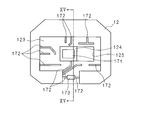
- FIG. 3 is a rear view showing the back side of the first substrate according to the first embodiment.
- It is a characteristic figure showing an example of a calculation result of capacity.
- It is a schematic diagram which shows the example of the model of a bonding wire in case the distance from a radiation detection element to an amplifier is 0.3 mm.
- It is a schematic diagram which shows the example of the model of a bonding wire in case the distance from a radiation detection element to an amplifier is 0.6 mm.
- FIG. 6 is a schematic cross-sectional view of a radiation detector according to Embodiment 2.
- FIG. 6 is a schematic cross-sectional view of a radiation detector according to Embodiment 3.
- FIG. 6 is a plan view of a first substrate according to Embodiment 3.
- FIG. 6 is a schematic cross-sectional view of a radiation detector according to Embodiment 4.
- FIG. 6 is a schematic perspective view of a radiation detector according to Embodiment 5.
- FIG. 6 is a plan view of a radiation detector according to Embodiment 5.
- FIG. 10 is a schematic perspective view of a first substrate according to Embodiment 7.
- FIG. 10 is a schematic perspective view of a first substrate according to an eighth embodiment.
- FIG. 1 is a block diagram showing the configuration of the radiation detection apparatus.
- the radiation detection apparatus is, for example, a fluorescent X-ray analysis apparatus.
- the radiation detection apparatus includes a radiation source 4 that irradiates a sample 6 with radiation such as an electron beam or an X-ray, a sample stage 5 on which the sample 6 is placed, and a radiation detector 1. Radiation is irradiated from the radiation source 4 to the sample 6, radiation such as fluorescent X-rays is generated in the sample 6, and the radiation detector 1 detects the radiation generated from the sample 6. In the figure, the radiation is indicated by arrows.
- the radiation detector 1 outputs a signal proportional to the detected radiation energy.
- the radiation detector 1 is connected to a signal processing unit 2 that processes the output signal.
- the signal processing unit 2 counts each value signal output from the radiation detector 1 and performs a process of generating a relationship between the radiation energy and the count number, that is, a radiation spectrum.
- the signal processing unit 2 is connected to the analysis unit 32.
- the analysis unit 32 includes a calculation unit that performs a calculation and a memory that stores data.
- the signal processing unit 2, the analysis unit 32, and the radiation source 4 are connected to the control unit 31.
- the control unit 31 controls operations of the signal processing unit 2, the analysis unit 32, and the radiation source 4.
- the signal processing unit 2 outputs data indicating the generated spectrum to the analysis unit 32.
- the analysis unit 32 receives data from the signal processing unit 2 and performs qualitative analysis or quantitative analysis of elements contained in the sample 6 based on the spectrum indicated by the input data.
- a display unit 33 such as a liquid crystal display is connected to the analysis unit 32.
- the display unit 33 displays the analysis result by the analysis unit 32.
- the display unit 33 displays the spectrum generated by the signal processing unit 2.
- the control unit 31 may be configured to receive a user operation and control each unit of the radiation detection apparatus in accordance with the received operation. Moreover, the control part 31 and the analysis part 32 may be comprised with the same computer. Further, the radiation detection apparatus may be in a form that does not include the radiation source 4, the sample stage 5, the analysis unit 32, or the display unit 33.
- FIG. 2 is a schematic cross-sectional view of the radiation detector 1 according to the first embodiment.
- the radiation detector 1 includes a plate-like stem bottom portion 135.
- a cap-shaped cover 15 is covered on one surface side of the stem bottom portion 135.
- the cover 15 has a shape in which a truncated cone is connected to one end of a cylinder, and the other end of the cylinder is joined to the stem bottom portion 135.
- the inside of the cover 15 is hermetically sealed and decompressed or filled with an inert gas.
- the stem bottom part 135, the cover 15 and the window 151 constitute a housing of the radiation detector 1.
- the first substrate 12 has a first surface 121 that faces the window 151.
- the first substrate 12 is preferably formed of a material that generates as little radiation as possible by radiation.
- the material of the first substrate 12 is, for example, ceramic.
- the radiation detection element 11 is a semiconductor element, for example, an SDD (Silicon Drift Detector).
- the radiation detection element 11 is provided on the first surface 121 of the first substrate 12 and is disposed at a position facing the window 151.
- the collimator 131 is formed in a cylindrical shape having both ends opened with a material that shields radiation, and is disposed between the radiation detection element 11 and the window 151. One end of the collimator 131 faces the window 151, and the other end faces the surface of the radiation detection element 11.
- the collimator 131 may be in contact with the surface of the radiation detection element 11 or may be adhered to the radiation detection element 11 with an adhesive.
- the collimator 131 shields part of the radiation that has passed through the window 151, and the radiation detection element 11 detects radiation that has not been shielded by the collimator 131.
- a bonding pad 122 is provided on the first surface 121 of the first substrate 12.
- the bonding pad 122 is connected to the radiation detection element 11 via the bonding wire 161.
- a shielding plate 132 is disposed behind the first substrate 12 with the direction from the first surface 121 toward the window 151 as the front.
- the shielding plate 132 shields radiation from the rear.
- the shielding plate 132 shields fluorescent X-rays generated from the Peltier element 133 or the second substrate 14 described later. In this way, the shielding plate 132 suppresses radiation from entering the radiation detection element 11 from behind.
- the shielding plate 132 is in thermal contact with the heat absorbing portion of the Peltier element 133. That is, the shielding plate 132 is interposed between the first substrate 12 and the Peltier element 133.
- the radiation detector 1 includes a cold finger 134 that is in thermal contact with the heat dissipation portion of the Peltier element 133.
- the cold finger 134 is made of a material having high thermal conductivity.
- the cold finger 134 includes a plate-like portion that is in thermal contact with the heat dissipation portion of the Peltier element 133 and a bolt-like portion that protrudes from the plate-like portion.
- the bolt-shaped portion of the cold finger 134 passes through the stem bottom portion 135 and protrudes from the outer surface of the stem bottom portion 135.
- the shielding plate 132 and the Peltier element 133, and the Peltier element 133 and the cold finger 134 may be in direct contact with each other, and a heat conductive material may be interposed therebetween.
- the bolt-shaped portion of the cold finger 134 is connected to a heat radiating portion outside the radiation detector 1.
- the heat radiating portion is, for example, a heat radiating plate.
- the radiation detection element 11 is cooled by the Peltier element 133 through the first substrate 12 and the shielding plate 132.
- the heat of the radiation detection element 11 is conducted from the Peltier element 133 to the cold finger 134 and is radiated from the heat radiation portion.
- the radiation detector 1 may not have the shielding plate 132.
- the radiation detector 1 includes a second substrate 14 and a plurality of lead pins 142.
- the second substrate 14 has an annular shape and is arranged around the Peltier element 133 or the cold finger 134.
- a bonding pad 141 is provided on the second substrate 14.
- the bonding pad 141 is connected to the bonding pad 122 via the bonding wire 162.
- the lead pin 142 passes through the stem bottom portion 135.
- One end of the lead pin 142 is connected to the second substrate 14.
- the lead pin 142 is connected to the bonding pad 141 via a wiring or a bonding wire (not shown).
- the lead pins 142 are used to supply power and input / output signals to the radiation detection element 11.
- the radiation detector 1 may not include the second substrate 14 and may have a form in which the bonding wires 162 are directly connected to the lead pins 142.
- the stem bottom 135, the cold finger 134, and the lead pin 142 constitute a stem.
- FIG. 3 is a schematic cross-sectional view showing an example of a detailed structure of the first substrate 12 according to the first embodiment.
- FIG. 4 is a rear view showing the back side of the first substrate 12 according to the first embodiment.
- the first substrate 12 has a second surface 123 and a third surface 124 on the back side of the first surface 121.
- the second surface 123 and the third surface 124 are back surfaces with respect to the first surface 121.
- the third surface 124 is formed at a position where a part of the back surface with respect to the first surface 121 is recessed from the second surface 123.
- substrate 12 is a shape from which the thickness from the 1st surface 121 differs partially.
- the distance between the first surface 121 and the second surface 123 is longer than the distance between the first surface 121 and the third surface 124. Furthermore, a through hole 125 is formed in the first substrate 12 so as to penetrate between the first surface 121 and the third surface 124.
- the first surface 121, the second surface 123, and the third surface 124 may or may not be parallel.
- An amplifier 171 is provided on the third surface 124.
- the amplifier 171 is connected to the radiation detection element 11 via a bonding wire 163.
- the bonding wire 163 is disposed so as to pass through the through hole 125.
- a plurality of wirings 172 are provided on the second surface 123.
- Various components 173 such as a capacitor necessary for the operation of the radiation detector 1 are provided on the second surface 123.
- the amplifier 171 is connected to the wiring 172 through the bonding wire 164.
- the radiation detection element 11 is connected to the wiring 172 via a bonding wire (not shown).
- the wiring 172 is connected to the bonding pad 122 through a conductive portion (not shown) provided in the first substrate 12 or is connected to the lead pin 142 via a bonding wire (not shown).
- the amplifier 171 is a preamplifier, for example.
- the radiation detection element 11 outputs a signal proportional to the detected radiation energy, and the output signal is input to the amplifier 171 through the bonding wire 163.
- the amplifier 171 performs signal conversion and amplification.
- the converted / amplified signal is output from the amplifier 171 and output to the outside of the radiation detector 1 through the bonding wire 164, the wiring 172 and the lead pin 142. In this way, the radiation detector 1 outputs a signal proportional to the energy of the radiation detected by the radiation detection element 11.
- the distance between the first surface 121 and the second surface 123 is longer than the distance between the first surface 121 and the third surface 124, the distance between the radiation detection element 11 and the wiring 172 is radiation. It is longer than the distance between the detection element 11 and the amplifier 171.
- the distance between the first surface 121 and the second surface 123 is at least twice the distance between the first surface 121 and the third surface 124.
- the distance between the first surface 121 and the third surface 124 is 0.3 mm
- the distance between the first surface 121 and the second surface 123 is 0.6 mm.
- characteristic X-rays may be generated from the wiring 172 when the radiation is applied to the wiring 172, and this characteristic X-ray may enter the radiation detection element 11.
- the characteristic X-ray from the wiring 172 is detected by the radiation detection element 11, and the spectrum generated by the signal processing unit 2 includes a peak due to the characteristic X-ray from the wiring 172.
- the peaks included in the spectrum of the radiation detected by the radiation detector 1 it becomes difficult to accurately obtain the intensity of the peak that overlaps the peak caused by the characteristic X-ray from the wiring 172, and the accuracy of radiation detection deteriorates. .
- the distance between the first surface 121 and the second surface 123 is set to a sufficient length such that the intensity of the characteristic X-ray from the wiring 172 incident on the radiation detection element 11 is sufficiently small. ing.
- the distance between the first surface 121 and the second surface 123 is such that the characteristic X-ray generated in the wiring 172 can be sufficiently absorbed by the first substrate 12 between the wiring 172 and the radiation detection element 11.
- the intensity of the characteristic X-ray from the wiring 172 incident on the radiation detection element 11 does not have to be completely zero, and is such that the result of detecting the characteristic X-ray from the wiring 172 does not affect the spectrum analysis result. It only needs to be smaller. For example, it is only necessary that the intensity of the characteristic X-rays is reduced to such an extent that the intensity of the peak derived from the characteristic X-rays included in the spectrum is about the same as that of the noise and it is difficult to confirm the peak derived from the characteristic X-rays. In this way, by setting the distance between the first surface 121 and the second surface 123, it is possible to suppress erroneous detection by the radiation detection device as the radiation to be analyzed for the characteristic X-ray generated in the wiring 172. Is done.
- the distance between the first surface 121 and the second surface 123 should be calculated so that the influence of the characteristic X-ray detection result at the radiation detection element 11 is sufficiently small in consideration of the following parameters: Can do.
- the parameters include the intensity of the radiation that passes through the radiation detection element 11, the radiation transmittance at the first substrate 12, the radiation absorption rate at the wiring 172, and the wiring 172 that absorbs radiation generates characteristic X-rays Fluorescence yield corresponding to the probability of generation, transmittance of characteristic X-rays on the first substrate 12, and absorption rate of characteristic X-rays on the radiation detection element 11 are included.
- the distance between the first surface 121 and the second surface 123 can be determined experimentally. By performing radiation detection using a plurality of radiation detectors 1 having different distances between the first surface 121 and the second surface 123, the characteristic X-ray detection result does not affect the spectrum analysis result. The distance is determined.
- the bonding wire 163 connecting the radiation detection element 11 and the amplifier 171 is longer, the parasitic capacitance of the bonding wire 163 increases and the input capacitance of the amplifier 171 increases. As the input capacitance increases, noise included in the signal output from the amplifier 171 increases. As a result, the half width of the peak included in the spectrum of the radiation detected by the radiation detector 1 is increased, and the energy resolution when specifying the radiation according to the energy is deteriorated.
- the amplifier 171 on the third surface 124 by providing the amplifier 171 on the third surface 124, the radiation detection element 11 is connected via the radiation detection element 11 and the bonding wire 163 of the amplifier 171 as compared with the case where the amplifier 171 is provided on the second surface 123.
- the distance to the portion connected to is shortened, and the length of the required bonding wire 163 is shortened. Therefore, the parasitic capacitance of the bonding wire 163 is reduced, the input capacitance of the amplifier 171 is reduced, and the signal output from the amplifier 171 is compared with the case where the amplifier 171 is provided on the second surface 123 without providing the third surface 124.
- the noise resolution of the radiation detector 1 is improved.
- the parasitic capacitance of the bonding wire 163 and the energy resolution of the radiation detector 1 will be described. According to T. SAKURAI and K. TAMARU, "Simple Formulas for Two- and Three-Dimensional Capacitances", IEEE TRANSACTION ON ELECTRON DEVICES, VOL. ED-30, NO. 2, February 1983
- the capacity C per unit length of the bonding wire can be approximated by the following equation (1).
- FIG. 5 is a characteristic diagram illustrating an example of the calculation result of the capacity.
- the horizontal axis indicates the distance t in units of mm, and the vertical axis indicates the capacity per 1 mm of bonding wire.
- the solid line in the figure shows an approximate expression that approximates the calculation result of the capacity.
- the approximate expression, a horizontal axis x, a vertical axis y, a y 10.587x -0.268.
- the capacity of the bonding wire 163 was calculated based on the capacity calculation result shown in FIG.
- the capacitance of the bonding wire 163 was calculated when the distance from the radiation detection element 11 to the amplifier 171 was 0.3 mm and when the distance from the radiation detection element 11 to the amplifier 171 was 0.6 mm.
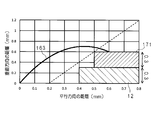
- FIG. 6 is a schematic diagram showing an example of a model of the bonding wire 163 when the distance from the radiation detection element 11 to the amplifier 171 is 0.3 mm.
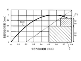
- FIG. 7 is a schematic diagram illustrating an example of a model of the bonding wire 163 when the distance from the radiation detection element 11 to the amplifier 171 is 0.6 mm.
- the horizontal axis represents the distance in the direction parallel to the first surface 121 from the connection point between the radiation detection element 11 and the bonding wire 163.
- the vertical axis represents the distance in the direction perpendicular to the first surface 121 from the connection point between the radiation detection element 11 and the bonding wire 163.
- the broken lines shown in FIGS. 6 and 7 are lines that limit the positions of the first substrate 12 and the amplifier 171. In order to secure a visual field at the time of bonding, it is necessary that the first substrate 12 or the amplifier 171 is not located above the line indicated by the broken line. When the first substrate 12 or the amplifier 171 is positioned above the line shown by the broken line, the length of the bonding wire 163 becomes longer.
- the capacity of the bonding wire 163 having the shape and length shown in FIGS. 6 and 7 was calculated.
- the capacity of each part obtained by dividing the bonding wire 163 was calculated, and the capacity of each part was added to calculate the capacity of the entire bonding wire 163.
- the calculated value of the capacitance was 17.6 fF.
- the calculated value of the capacitance was 21.4 fF.
- the distance from the radiation detection element 11 to the amplifier 171 is 0.3 mm, this corresponds to the case where the amplifier 171 is provided on the second surface 123, and when the distance from the radiation detection element 11 to the amplifier 171 is 0.6 mm. This corresponds to the case where the amplifier 171 is provided on the second surface 123 without providing the third surface 124.
- the provision of the amplifier 171 on the third surface 124 reduces the length of the bonding wire 163 compared to the case where the amplifier 171 is provided on the second surface 123.
- the parasitic capacitance of the bonding wire 163 is reduced.
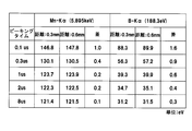
- FIG. 8 is a chart showing an example of the calculation result of the half width of the peak included in the radiation spectrum.
- the temperature of the radiation detection element 11 cooled by the Peltier element 133 is ⁇ 40 ° C., and the leakage current of the radiation detection element 11 is 0.01 pA.
- the full width at half maximum was calculated for the peak of K ⁇ of Mn (manganese) with an energy of 5.895 keV and the peak of K ⁇ of B (boron) with an energy of 188.3 eV.
- the half width was calculated for the case where the distance from the radiation detection element 11 to the amplifier 171 was 0.3 mm and for the case where the distance from the radiation detection element 11 to the amplifier 171 was 0.6 mm.
- the half width of the peak was calculated for each of peaking times of 0.1 ⁇ s, 0.3 ⁇ s, 1 ⁇ s, 2 ⁇ s, and 8 ⁇ s.
- the peaking time is a time constant when performing a moving average on the signal from the radiation detector 1 in the signal processing in the signal processing unit 2. As the peaking time increases, the noise decreases and the half width of the peak decreases, but the dead time increases.
- the unit of the calculation result of the half width of the peak shown in FIG. 8 is eV.
- the half width when the distance from the radiation detection element 11 to the amplifier 171 is 0.3 mm is smaller than the half width when the distance from the radiation detection element 11 to the amplifier 171 is 0.6 mm. It has become.
- the peaking time is 0.1 ⁇ s
- the half-value widths of the K ⁇ peaks of Mn are different from each other by 1.0 eV. The smaller the half width of the peak, the easier it is to separate the peaks contained in the spectrum and the higher the energy resolution.
- the provision of the amplifier 171 on the third surface 124 reduces the peak half-value width compared to the case where the amplifier 171 is provided on the second surface 123, thereby detecting radiation. High energy resolution at the time.
- the distance between the first surface 121 and the second surface 123 on which the radiation detection element 11 is provided is the distance between the first surface 121 and the third surface 124.
- the amplifier 171 is provided on the third surface 124 and the wiring 172 is provided on the second surface 123.
- the distance between the radiation detection element 11 and the wiring 172 can be made sufficiently long, and the incidence of the characteristic X-ray from the wiring 172 on the radiation detection element 11 can be suppressed.
- the provision of the amplifier 171 on the third surface 124 prevents the distance between the radiation detection element 11 and the amplifier 171 from being increased, and the bonding wire 163 that connects the radiation detection element 11 and the amplifier 171. An increase in the length of is prevented.
- the radiation detection apparatus can achieve both high accuracy of radiation detection and high energy resolution.
- the form in which the entire amplifier 171 is mainly provided in the radiation detector 1 is shown.
- a part of the amplifier 171 is provided in the radiation detector 1 and This part may be provided outside the radiation detector 1.
- a part of the amplifier 171 is provided on the third surface 124 of the first substrate 12, and is connected to the radiation detection element 11 via a bonding wire 163.
- an FET Field effect transistor
- the distance between the radiation detection element 11 and the wiring 172 is longer than the distance between the radiation detection element 11 and the portion connected to the radiation detection element 11 via the bonding wire 163 of the amplifier 171.
- the other part of the amplifier 171 may be disposed between the radiation detector 1 and the signal processing unit 2 or may be configured integrally with the signal processing unit 2.
- FIG. 9 is a schematic cross-sectional view of the radiation detector 1 according to the second exemplary embodiment.
- the first substrate 12 has a fourth surface 126 facing the window 151. That is, the first surface 121 and the fourth surface 126 have substantially the same direction.
- the distance between the fourth surface 126 and the window 151 is longer than the distance between the first surface 121 and the window 151. That is, the fourth surface 126 is located behind the plane including the first surface 121.
- the fourth surface 126 is outside the first surface 121, that is, at a position farther from the end of the first surface 121 when viewed from a straight line passing through the center of the first surface 121 and intersecting the first surface 121.
- the bonding pad 122 is provided on the fourth surface 126.
- the bonding wire 161 connected to the radiation detection element 11 is connected to the bonding pad 122.
- the bonding wire 162 is connected between the bonding pad 122 and the bonding pad 141.
- Other configurations of the radiation detector 1 are the same as those of the first embodiment.
- Other configurations of the radiation detection apparatus are the same as those in the first embodiment.
- the bonding wire 162 connected to the bonding pad 122 passes through a position outside the first substrate 12.
- the bonding wire connected to the first substrate 12 and extending rearward from the first substrate 12 passes through a position outside the first substrate 12. For this reason, it is necessary to leave a gap through which the bonding wire passes between the first substrate 12 and the cover 15.
- the bonding wire 162 is connected to the bonding pad 122 on the first surface 121. In the present embodiment, since the bonding wire 162 is connected to the bonding pad 122 on the fourth surface 126 behind the first surface 121, the bonding wire 162 passes through a more rearward position.
- the cover 15 Since the shape of the cover 15 is tapered, the gap between the first substrate 12 and the cover 15 increases as the position of the bonding wire 162 is further rearward. Therefore, compared to the case where the first substrate 12 does not have the fourth surface 126 as shown in FIG. 2, in the present embodiment, the first substrate 12 is arranged closer to the window 151, or the first The substrate 12 can be made larger.
- the radiation detection element 11 provided on the first surface 121 is closer to the window 151. That is, in the present embodiment, the radiation detection element 11 can be disposed closer to the window 151.
- the radiation detection element 11 comes closer to the sample 6, and the solid angle through which the radiation incident on the radiation detection element 11 among the radiation generated in the sample 6 passes increases.
- the first substrate 12 is made larger, the area of the first surface 121 becomes larger, and the size of the radiation detection element 11 that can be provided on the first surface 121 increases. That is, in this embodiment, the size of the radiation detection element 11 can be increased.
- the present embodiment it is possible to improve the radiation detection sensitivity of the radiation detector 1 without changing the shape of the cover 15.
- the radiation detector 1 and the radiation detection apparatus may have a form in which the first substrate 12 does not have the third surface 124. If the radiation detector 1 includes the first substrate 12 having the first surface 121 as the first surface and the fourth surface 126 as the second surface, at least a part of the amplifier 171 and the wiring 172 are located at any position. Even if the radiation detection element 11 is disposed in the position, the radiation detection element 11 can be disposed closer to the window 151 or the size of the radiation detection element 11 can be increased.
- FIG. 10 is a schematic cross-sectional view of the radiation detector 1 according to the third embodiment.
- FIG. 11 is a plan view of the first substrate 12 according to the third embodiment.
- FIG. 11 is a view of the first substrate 12 as viewed from the front side, and shows a plurality of lead pins 142.
- the first substrate 12 has a notch 128 in which a part of the side surface 127 is recessed.
- FIG. 11 shows an example in which the first substrate 12 has eight cutout portions 128.
- the number of the notches 128 may be other numbers.
- Each lead pin 142 is disposed at a position along the notch 128.
- the leading end of the lead pin 142 is at a position close to a plane including the first surface 121.
- the wiring 172 is connected to the bonding pad 122 through a conductive portion (not shown) provided in the first substrate 12.
- the bonding pad 122 is connected to the lead pin 142 via the bonding wire 165.
- FIG. 10 shows an example in which the radiation detector 1 does not include the second substrate 14.
- the radiation detector 1 may include a second substrate 14.
- Other configurations of the radiation detector 1 are the same as those of the first embodiment.
- Other configurations of the radiation detection apparatus are the same as those in the first embodiment.
- the bonding wire 162 that connects the bonding pad 122 and the bonding pad 141 on the second substrate 14 is more than the first substrate 12. Pass through the outer position.
- the lead pin 142 is disposed at a position along the notch 128, whereby the tip of the lead pin 142 can be disposed close to the bonding pad 122 on the first substrate 12.
- the bonding wire 165 that connects the bonding pad 122 and the lead pin 142 is shorter than the bonding wire 162 as shown in FIG. 2, and the size of the bonding wire 165 bulging outward from the first substrate 12 is smaller. For this reason, compared with the case where the 1st board
- substrate 12 and the cover 15 can be made narrower. It becomes possible. That is, by arranging the first substrate 12 closer to the window 151, the radiation detection element 11 can be arranged closer to the window 151. Alternatively, the size of the radiation detection element 11 can be increased by making the first substrate 12 larger. Thereby, the solid angle through which the radiation incident on the radiation detection element 11 among the radiation generated in the sample 6 passes increases, and the radiation detection sensitivity of the radiation detector 1 is improved. Therefore, also in the present embodiment, it is possible to improve the radiation detection sensitivity in the radiation detector 1 without changing the shape of the cover 15.
- the radiation detector 1 and the radiation detection apparatus may have a form in which the first substrate 12 does not have the third surface 124. If the lead pin 142 is arranged along the notch portion 128 of the first substrate 12, the radiation detection element 11 can be further connected to the window 151 regardless of the position of at least a part of the amplifier 171 and the wiring 172. It is possible to increase the size of the radiation detection element 11 or to arrange the radiation detection element 11.
- FIG. 12 is a schematic cross-sectional view of the radiation detector 1 according to the fourth embodiment.
- Bonding pads 129 are provided on the side surfaces 127 of the first substrate 12.
- the bonding pad 129 is connected to the lead pin 142 via the bonding wire 166.
- FIG. 12 shows an example in which the radiation detector 1 does not include the second substrate 14.
- the radiation detector 1 may include the second substrate 14, and the bonding pad 129 may be connected to the lead pin 142 via the second substrate 14.
- the bonding pad 122 is connected to the bonding pad 129 through a conductive portion (not shown) provided in the first substrate 12.
- the first substrate 12 does not include the bonding pad 122, and the radiation detection element 11 may be connected to the bonding pad 129 through a conductive portion (not shown) provided in the first substrate 12.
- the wiring 172 is connected to the bonding pad 129 through a conductive portion (not shown) provided in the first substrate 12.
- Other configurations of the radiation detector 1 are the same as those of the first embodiment.
- Other configurations of the radiation detection apparatus are the same as those in the first embodiment.
- the bonding wire 162 that connects the bonding pad 122 and the bonding pad 141 on the second substrate 14 is outside the first substrate 12. Pass through the position.
- the bonding wire 166 since the bonding wire 166 is connected to the bonding pad 129 provided on the side surface 127 of the first substrate 12, the bonding wire 166 passes through a position behind the bonding wire 162. Since the shape of the cover 15 is tapered, the gap between the first substrate 12 and the cover 15 increases as the position of the bonding wire is further rearward. For this reason, as shown in FIG.
- the radiation detection is performed by arranging the first substrate 12 closer to the window 151.
- the size of the element 11 can be increased.
- the size of the radiation detection element 11 can be increased by making the first substrate 12 larger.
- the radiation detector 1 and the radiation detection apparatus may have a form in which the first substrate 12 does not have the third surface 124. If the bonding wire 166 is connected to the side surface 127 of the first substrate 12, the radiation detection element 11 is brought closer to the window 151 regardless of the position of at least a part of the amplifier 171 and the wiring 172. It becomes possible to arrange or increase the size of the radiation detection element 11.
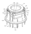
- FIG. 13 is a schematic perspective view of the radiation detector 1 according to the fifth exemplary embodiment.
- FIG. 14 is a plan view of the radiation detector 1 according to the fifth embodiment.
- FIG. 13 shows a view in which the cover 15 is omitted
- FIG. 14 shows a view in which the cover 15 and the collimator 131 are omitted.
- FIG. 13 is the figure which looked at the radiation detector 1 from the front side.
- the first substrate 12 has a polygonal shape in plan view. In the example shown in FIGS. 13 and 14, the first substrate 12 has a hexagonal shape, and the radiation detection element 11 has an octagonal shape.
- At least some of the plurality of corners of the first substrate 12 are disposed at positions that do not overlap with the corners of the radiation detection element 11 in plan view.
- a plurality of corner portions including the corners of the first substrate 12 and portions in the vicinity of the corners protrude outward from the radiation detection element 11 in plan view.
- the plurality of lead pins 142 are arranged at positions that do not overlap the radiation detection element 11 in plan view.
- the shape of the radiation detection element 11 may be a shape other than a polygon in plan view.
- the bonding pad 122 is provided on the corner portion of the first substrate 12. Each lead pin 142 is disposed at a position along one of the sides of the first substrate 12 in plan view.
- the wiring 172 is connected to the bonding pad 122 through a conductive portion (not shown) provided in the first substrate 12.
- the bonding pad 122 is connected to the lead pin 142 via the bonding wire 165.
- 13 and 14 show an example in which the radiation detector 1 does not include the second substrate 14.
- the radiation detector 1 may include a second substrate 14. Other configurations of the radiation detector 1 are the same as those of the first embodiment. Other configurations of the radiation detection apparatus are the same as those in the first embodiment.
- the radiation detection element 11 and the lead pin 142 are connected through the bonding pad 122 and the bonding wire 165 provided at the corner portion of the first substrate 12.
- the area of the corner portion that protrudes outward from the radiation detection element 11 in plan view may be an area where the bonding pad 122 can be provided.
- the lead pin 142 can be arranged as close as possible to the radiation detection element 11 in a plan view. For this reason, in this embodiment, it becomes possible to make the clearance gap between the radiation detection element 11 and the cover 15 narrower. That is, the radiation detection element 11 can be disposed closer to the window 151. Alternatively, the size of the radiation detection element 11 can be increased.
- the solid angle through which the radiation incident on the radiation detection element 11 among the radiation generated in the sample 6 passes increases, and the radiation detection sensitivity of the radiation detector 1 is improved. Therefore, also in the present embodiment, it is possible to improve the radiation detection sensitivity in the radiation detector 1 without changing the shape of the cover 15.
- the radiation detector 1 and the radiation detection apparatus may have a form in which the first substrate 12 does not have the third surface 124. If the connection between the radiation detection element 11 and the lead pin 142 is made via the bonding pad 122 provided at the corner portion of the first substrate 12, at least a part of the amplifier 171 and the wiring 172 are located at any position. Even if it is disposed, the radiation detection element 11 can be disposed closer to the window 151 or the size of the radiation detection element 11 can be increased.
- FIG. 15 is a schematic cross-sectional view of the radiation detection element 11, the collimator 131, and the first substrate 12 according to the sixth embodiment.
- FIG. 15 shows a cross section taken along line XV-XV in FIG.
- the component 173 is a component for temperature measurement or a component for ESD (electro-static discharge) countermeasures.
- the temperature measurement component 173 is, for example, a thermistor, a diode, a resistance temperature detector, or a thermocouple.
- the ESD countermeasure component 173 is, for example, a ceramic capacitor, a diode, or a varistor.
- the part 173 is arranged at a position that does not overlap with the sensitive part of the radiation detection element 11 in a plan view seen from the front side.
- the sensitive part of the radiation detection element 11 is a part that can detect the radiation incident from the front, and is a part located inside the inner surface of the cylindrical collimator 131.
- the component 173 is disposed outside the surface obtained by virtually extending the inner surface of the cylindrical collimator 131. More preferably, the component 173 is disposed outside the surface virtually extending the inner surface of the cylindrical collimator 131 and inside the surface virtually extending the outer surface of the cylindrical collimator 131.
- the component 173 is disposed on the inner side and as close as possible to the surface obtained by virtually extending the outer surface of the collimator 131.
- Other configurations of the radiation detector 1 are the same as those of the first embodiment.
- Other configurations of the radiation detection apparatus are the same as those in the first embodiment.
- the component 173 or the solder for attaching the component 173 to the first substrate 12 is irradiated with radiation, fluorescent X-rays are generated from the component 173 or the solder.
- the generated fluorescent X-rays are detected by the radiation detection element 11 without being absorbed by the first substrate 12, the accuracy of radiation detection deteriorates.
- the component 173 is arranged at a position that does not overlap the sensitive portion of the radiation detection element 11, so that fluorescent X-rays are generated from the component 173 or the solder, or the generated fluorescent X-rays are emitted from the radiation detection element. 11 is suppressed from being detected.
- the component 173 when the component 173 is arranged outside the surface virtually extending the inner surface of the cylindrical collimator 131 and inside the surface virtually extending the outer surface of the cylindrical collimator 131, The radiation that has entered the radiation detector 1 from above is shielded by the collimator 131 and is not applied to the component 173 or the solder. Further, when the component 173 is arranged at a position as close as possible to the inside of the surface obtained by virtually extending the outer surface of the collimator 131, the radiation incident obliquely to the surface of the radiation detection element 11 is detected. It is difficult to irradiate the component 173 or the solder.
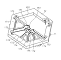
- FIG. 16 is a schematic perspective view of the first substrate 12 according to the seventh embodiment.
- FIG. 16 is a view of the first substrate 12 as seen from the rear side.
- a through hole 174 through which the bonding wire 163 does not pass is formed in the first substrate 12 in addition to the through hole 125.
- the through hole 174 is formed in a portion of the first substrate 12 where the wiring 172 is not provided.
- the through holes 174 may be formed only at one place of the first substrate 12 or may be formed at a plurality of places on the first substrate 12.
- FIG. 16 shows an example in which through holes 174 are formed at a plurality of locations on the first substrate 12.
- Other configurations of the radiation detector 1 are the same as those of the first embodiment.
- Other configurations of the radiation detection apparatus are the same as those in the first embodiment.
- the first substrate 12 When the first substrate 12 is irradiated with X-rays, scattered X-rays due to Compton scattering are generated from the first substrate 12. When the generated scattered X-rays are detected by the radiation detection element 11, the accuracy of radiation detection deteriorates.
- the first substrate 12 since the first substrate 12 has the through holes 174, the area of the first substrate 12 and the volume of the first substrate 12 with respect to X-rays incident from the front are reduced. As the area of the first substrate 12 with respect to incident X-rays decreases, the probability that X-rays enter the first substrate 12 decreases, and the frequency of occurrence of Compton scattering decreases.
- the volume of the first substrate 12 decreases, the frequency of occurrence of Compton scattering in the first substrate 12 decreases. For this reason, it is suppressed that the scattered X-rays by Compton scattering are detected by the radiation detection element 11, and it is suppressed that the precision of a radiation detection deteriorates. Therefore, in the present embodiment, it is possible to further improve the radiation detection sensitivity of the radiation detector 1.
- FIG. 17 is a schematic perspective view of the first substrate 12 according to the eighth embodiment.
- FIG. 17 is a view of the first substrate 12 as viewed from the rear side.
- the first substrate 12 has a thin plate portion 175 that is thinner than the portion where the wiring 172 is provided.
- the thin plate portion 175 is formed on a portion of the first substrate 12 where the wiring 172 is not provided.
- the thin plate portion 175 may be provided at only one location of the first substrate 12 or may be provided at a plurality of locations on the first substrate 12.
- FIG. 17 shows an example in which thin plate portions 175 exist at a plurality of locations on the first substrate 12.
- Other configurations of the radiation detector 1 are the same as those of the first embodiment.
- Other configurations of the radiation detection apparatus are the same as those in the first embodiment.
- the volume of the first substrate 12 is reduced. As the volume of the first substrate 12 decreases, the frequency with which X-rays enter the first substrate 12 and Compton scattering occurs decreases. For this reason, it is suppressed that the scattered X-rays by Compton scattering are detected by the radiation detection element 11, and it is suppressed that the precision of a radiation detection deteriorates. Therefore, in the present embodiment, it is possible to further improve the radiation detection sensitivity of the radiation detector 1.
- the form which combined Embodiment 7 and 8 may be sufficient as the radiation detector 1 and the radiation detection apparatus. That is, the first substrate 12 may have a through hole 174 and a thin plate portion 175 through which the bonding wire 163 does not pass. Even in this embodiment, it is possible to further improve the radiation detection sensitivity of the radiation detector 1.
Landscapes
- Physics & Mathematics (AREA)
- Health & Medical Sciences (AREA)
- Life Sciences & Earth Sciences (AREA)
- General Physics & Mathematics (AREA)
- High Energy & Nuclear Physics (AREA)
- Molecular Biology (AREA)
- Spectroscopy & Molecular Physics (AREA)
- Chemical & Material Sciences (AREA)
- Analytical Chemistry (AREA)
- Biochemistry (AREA)
- General Health & Medical Sciences (AREA)
- Immunology (AREA)
- Pathology (AREA)
- Measurement Of Radiation (AREA)
- Analysing Materials By The Use Of Radiation (AREA)
- Light Receiving Elements (AREA)
Abstract
配線からの特性X線の放射線検出素子への入射を抑制しながらも、放射線検出器のエネルギー分解能の悪化を防止することができる放射線検出器及び放射線検出装置を提供する。 基板と、基板に設けられた放射線検出素子と、放射線検出素子に接続された増幅器の少なくとも一部と、基板に設けられた配線とを備える放射線検出器において、増幅器の少なくとも一部は、基板に設けられており、放射線検出素子と配線との間の距離が、放射線検出素子と増幅器の少なくとも一部との間の距離よりも長い。
Description
本発明は、放射線検出器及び放射線検出装置に関する。
X線等の放射線を検出する放射線検出器には、半導体製の放射線検出素子を用いたものがある。放射線検出素子は、基板の表面に設けられている。放射線検出器には、放射線検出素子が出力する信号を増幅するプリアンプ等の増幅器の少なくとも一部が設けられ、放射線検出素子に増幅器が接続されている。放射線検出素子と増幅器とを繋ぐボンディングワイヤの長さを可及的に短くするために、増幅器の少なくとも一部が基板の背面に配置されていることがある。特許文献1には、増幅器が基板の裏面に配置された放射線検出器が記載されている。
基板の裏面に増幅器が配置された放射線検出器では、基板の裏面に配線が設けられている。基板及び配線の材質によっては、基板の裏面に設けられた配線に放射線が入射して発生した特性X線が放射線検出素子へ入射することがある。基板の材質によっては、配線の材料が限られ、特性X線の強度が高い材料で配線が構成される場合がある。このような場合、配線からの特性X線の放射線検出素子への入射は、基板の厚みを大きくすることによって減少させることができる。しかしながら、基板の厚みを大きくした場合、基板の裏面に配置された増幅器の放射線検出素子に接続される部分と放射線検出素子との間の距離が長くなり、増幅器と放射線検出素子とを接続するボンディングワイヤの長さが長くなる。ボンディングワイヤの長さが長い場合、ボンディングワイヤによる寄生容量が増加し、増幅器の入力容量が増加する。入力容量が増加した結果、増幅器でノイズが増加し、放射線検出器のエネルギー分解能が悪化する。
本発明は、斯かる事情に鑑みてなされたものであって、その目的とするところは、配線からの特性X線の放射線検出素子への入射を抑制しながらも、放射線検出器のエネルギー分解能の悪化を防止することができる放射線検出器及び放射線検出装置を提供することにある。
本発明に係る放射線検出器は、基板と、該基板に設けられた放射線検出素子と、該放射線検出素子に接続された増幅器の少なくとも一部と、前記基板に設けられた配線とを備える放射線検出器において、前記増幅器の少なくとも一部は、前記基板に設けられており、前記放射線検出素子と前記配線との間の距離が、前記放射線検出素子と前記増幅器の少なくとも一部との間の距離よりも長いことを特徴とする。
本発明に係る放射線検出器は、前記基板は、前記放射線検出素子が設けられる第1面と、前記第1面の裏側に位置する第2面及び第3面とを有し、前記第1面と前記第2面との間の距離は、前記第1面と前記第3面との間の距離よりも長く、前記増幅器の少なくとも一部は、前記第3面に設けられており、前記配線は、前記第2面上に設けられていることを特徴とする。
本発明に係る放射線検出器は、前記基板は、前記第1面と前記第3面との間を貫通する貫通孔を更に有し、前記増幅器は、前記貫通孔を通るワイヤを介して前記放射線検出器に接続されていることを特徴とする。
本発明に係る放射線検出器は、放射線が通過する窓を有し、該窓に向けて先細りになったハウジングを更に備え、前記基板は、前記ハウジング内に配置され、前記第1面は、前記窓に対向しており、前記基板は、前記窓に対向した第4面を更に有し、前記第4面は、前記第1面よりも外側に位置しており、前記第4面と前記窓との間の距離は、前記第1面と前記窓との間の距離よりも長く、前記第4面に、ワイヤが接続されていることを特徴とする。
本発明に係る放射線検出器は、ハウジングと、リードピンとを更に備え、前記基板は、側面の一部が窪んだ切り欠き部を有し、前記ハウジング内に配置されており、前記リードピンは、前記切り欠き部に沿った位置に配置され、ワイヤを介して前記基板に接続されていることを特徴とする。
本発明に係る放射線検出器は、放射線が通過する窓を有し、該窓に向けて先細りになったハウジングを更に備え、前記基板は、前記ハウジング内に配置され、前記基板の側面に、ワイヤが接続されていることを特徴とする。
本発明に係る放射線検出装置は、検出した放射線のエネルギーに応じた信号を出力する本発明に係る放射線検出器と、該放射線検出器が出力した信号に基づいて、前記放射線のスペクトルを生成する信号処理部とを備えることを特徴とする。
本発明に係る放射線検出装置は、試料へ放射線を照射する線源と、前記試料から発生した放射線を検出し、検出した放射線のエネルギーに応じた信号を出力する本発明に係る放射線検出器と、該放射線検出器が出力した信号に基づいて、前記放射線のスペクトルを生成する信号処理部と、該信号処理部が生成したスペクトルの分析を行う分析部と、該分析部による分析結果を表示する表示部とを備えることを特徴とする。
本発明においては、基板に設けられた放射線検出素子と基板に設けられた配線との間の距離が、放射線検出素子と基板に設けられた増幅器の少なくとも一部との間の距離に比べて、長い。放射線検出素子と配線との間の距離を長くすることによって、配線からの特性X線を、放射線検出素子と配線との間でより効果的に吸収することが可能となり、特性X線が放射線検出素子へ入射することが抑制される。また、放射線検出素子と増幅器の少なくとも一部との間の距離を短くすることができ、放射線検出素子と増幅器との間を接続するボンディングワイヤの長さを短くし、ボンディングワイヤの寄生容量を減少させることができる。この結果、増幅器の入力容量の増加を防止し、放射線検出器のエネルギー分解能の悪化を防止することができる。
また、本発明においては、基板は、放射線検出素子が設けられる第1面の裏側に、配線が設けられる第2面と、増幅器の少なくとも一部が設けられる第3面とを有している。第1面と第2面との間の距離は、第1面と第3面との間の距離よりも長い。これにより、放射線検出素子と配線との間の距離が、放射線検出素子と増幅器の少なくとも一部との間の距離に比べて長くなる。
また、本発明においては、基板は、第1面と第3面との間を貫通する貫通孔を有している。貫通孔を通るボンディングワイヤにより、放射線検出素子と増幅器とが接続される。
また、本発明においては、放射線検出器は、放射線が通過する窓に向けて先細りになったハウジングを備え、基板はハウジング内に配置されている。第1面は窓に対向している。基板は、窓に対向し、第1面よりも外側に位置する第4面を有する。第4面と窓との間の距離は、第1面と窓との間の距離よりも長い。第4面には、ボンディングワイヤが接続されている。基板が第4面を有していない場合に比べて、ボンディングワイヤが通る基板とハウジングとの間の隙間がより大きくなる。このため、基板をより窓に近づけて配置すること、又は基板をより大きくすることが可能となる。
また、本発明においては、基板は側面の一部が窪んだ切り欠き部を有し、リードピンが切り欠き部に沿って配置されている。リードピンはボンディングワイヤを介して基板に接続されている。ボンディングワイヤが基板の外側へ膨らむ大きさが小さくなる。このため、基板をより窓に近づけて配置すること、又は基板をより大きくすることが可能となる。
また、本発明においては、基板の側面には、ボンディングワイヤが接続されている。基板の側面にボンディングパッドが接続されていない場合に比べて、ボンディングワイヤが通る基板とハウジングとの間の隙間がより大きくなる。このため、基板をより窓に近づけて配置すること、又は基板をより大きくすることが可能となる。
本発明にあっては、放射線検出素子と配線との間の距離が長いことにより、配線からの特性X線の放射線検出素子への入射が抑制される。また、放射線検出素子と増幅器の少なくとも一部との間の距離が短いことにより、放射線検出器のエネルギー分解能の悪化を防止することができる。従って、放射線検出装置は、放射線検出時に配線から発生する特性X線を誤検出することの抑制と、エネルギー分解能の高さとを両立させることが可能となる等、本発明は優れた効果を奏する。
以下本発明をその実施の形態を示す図面に基づき具体的に説明する。
<実施形態1>
図1は、放射線検出装置の構成を示すブロック図である。放射線検出装置は、例えば蛍光X線分析装置である。放射線検出装置は、試料6に電子線又はX線等の放射線を照射する線源4と、試料6が載置される試料台5と、放射線検出器1とを備えている。線源4から試料6へ放射線が照射され、試料6では蛍光X線等の放射線が発生し、放射線検出器1は試料6から発生した放射線を検出する。図中には、放射線を矢印で示している。放射線検出器1は、検出した放射線のエネルギーに比例した信号を出力する。放射線検出器1には、出力した信号を処理する信号処理部2が接続されている。信号処理部2は、放射線検出器1が出力した各値の信号をカウントし、放射線のエネルギーとカウント数との関係、即ち放射線のスペクトルを生成する処理を行う。
<実施形態1>
図1は、放射線検出装置の構成を示すブロック図である。放射線検出装置は、例えば蛍光X線分析装置である。放射線検出装置は、試料6に電子線又はX線等の放射線を照射する線源4と、試料6が載置される試料台5と、放射線検出器1とを備えている。線源4から試料6へ放射線が照射され、試料6では蛍光X線等の放射線が発生し、放射線検出器1は試料6から発生した放射線を検出する。図中には、放射線を矢印で示している。放射線検出器1は、検出した放射線のエネルギーに比例した信号を出力する。放射線検出器1には、出力した信号を処理する信号処理部2が接続されている。信号処理部2は、放射線検出器1が出力した各値の信号をカウントし、放射線のエネルギーとカウント数との関係、即ち放射線のスペクトルを生成する処理を行う。
信号処理部2は、分析部32に接続されている。分析部32は、演算を行う演算部及びデータを記憶するメモリを含んで構成されている。信号処理部2、分析部32及び線源4は、制御部31に接続されている。制御部31は、信号処理部2、分析部32及び線源4の動作を制御する。信号処理部2は、生成したスペクトルを示すデータを分析部32へ出力する。分析部32は、信号処理部2からのデータを入力され、入力されたデータが示すスペクトルに基づいて、試料6に含まれる元素の定性分析又は定量分析を行う。分析部32には、液晶ディスプレイ等の表示部33が接続されている。表示部33は、分析部32による分析結果を表示する。また、表示部33は、信号処理部2が生成したスペクトルを表示する。制御部31は、使用者の操作を受け付け、受け付けた操作に応じて放射線検出装置の各部を制御する構成であってもよい。また、制御部31及び分析部32は同一のコンピュータで構成されていてもよい。また、放射線検出装置は、線源4、試料台5、分析部32、又は表示部33を備えていない形態であってもよい。
図2は、実施形態1に係る放射線検出器1の模式的断面図である。放射線検出器1は、板状のステム底部135を備えている。ステム底部135の一面側には、キャップ状のカバー15が被さっている。カバー15は、円筒の一端に切頭錐体が連結した形状になっており、円筒の他端はステム底部135に接合している。カバー15の先端の切頭部分には、ベリリウム等の放射線を通過させる材料で形成された窓151が設けられている。即ち、カバー15の一部の形状は、窓151に向けて先細りの形状になっている。カバー15の内側は、密閉されており、減圧されているか、又は不活性ガスが充填されている。ステム底部135、カバー15及び窓151は、放射線検出器1のハウジングを構成している。
カバー15の内側には、筒状のコリメータ131と、放射線検出素子11と、第1基板12と、遮蔽板132と、ペルチェ素子133とが配置されている。第1基板12は、窓151に対向する第1面121を有している。第1基板12は、放射線の照射による放射線の発生が可及的に少ない材質で形成されていることが望ましい。第1基板12の材質は、例えばセラミックである。放射線検出素子11は、半導体製の素子であり、例えばSDD(Silicon Drift Detector)である。放射線検出素子11は、第1基板12の第1面121に設けられており、窓151に対向する位置に配置されている。コリメータ131は、放射線を遮蔽する材料で両端が開口した筒状に形成されており、放射線検出素子11と窓151との間に配置されている。コリメータ131の一端は窓151に対向しており、他端は放射線検出素子11の表面に対向している。コリメータ131は、放射線検出素子11の表面に接していてもよく、接着剤により放射線検出素子11に接着されていてもよい。コリメータ131は、窓151を通過した放射線の一部を遮蔽し、放射線検出素子11は、コリメータ131で遮蔽されなかった放射線を検出する。
第1基板12の第1面121上には、ボンディングパッド122が設けられている。ボンディングパッド122は、ボンディングワイヤ161を介して放射線検出素子11に接続されている。第1面121から窓151へ向かう向きを前方として、第1基板12の後方には、遮蔽板132が配置されている。遮蔽板132は、後方からの放射線を遮蔽する。例えば、遮蔽板132は、ペルチェ素子133又は後述する第2基板14から発生する蛍光X線を遮蔽する。このようにして、遮蔽板132は、放射線検出素子11へ後方から放射線が入射することを抑制する。遮蔽板132は、ペルチェ素子133の吸熱部分に熱的接触している。即ち、遮蔽板132は、第1基板12とペルチェ素子133との間に介在している。
また、放射線検出器1は、ペルチェ素子133の放熱部分に熱的接触したコールドフィンガー134を備えている。コールドフィンガー134は、熱伝導率が高い材料で形成されている。コールドフィンガー134は、ペルチェ素子133の放熱部分に熱的接触した板状部分と、板状部分から突出したボルト状部分とを含んで構成されている。コールドフィンガー134のボルト状部分は、ステム底部135を貫通しており、ステム底部135の外面から突出している。遮蔽板132及びペルチェ素子133、並びにペルチェ素子133及びコールドフィンガー134は、互いに直接接触していてもよく、間に熱伝導材を介在させていてもよい。コールドフィンガー134のボルト状部分は、放射線検出器1外の放熱部に連結される。放熱部は例えば放熱板である。放射線検出素子11は、第1基板12及び遮蔽板132を通してペルチェ素子133によって冷却される。放射線検出素子11の熱は、ペルチェ素子133からコールドフィンガー134へ伝導し、放熱部から放熱される。なお、放射線検出器1は、遮蔽板132を備えていない形態であってもよい。
また、放射線検出器1は、第2基板14と、複数のリードピン142とを備えている。第2基板14は、環状であり、ペルチェ素子133又はコールドフィンガー134の周囲に配置されている。第2基板14上には、ボンディングパッド141が設けられている。ボンディングパッド141は、ボンディングワイヤ162を介してボンディングパッド122に接続されている。リードピン142は、ステム底部135を貫通している。リードピン142の一端は第2基板14に連結している。リードピン142は図示しない配線又はボンディングワイヤを介してボンディングパッド141に接続されている。リードピン142を用いて、放射線検出素子11に対する電力の供給及び信号の入出力が行われる。なお、放射線検出器1は、第2基板14を備えておらず、ボンディングワイヤ162が直接にリードピン142に接続された形態であってもよい。ステム底部135、コールドフィンガー134及びリードピン142は、ステムを構成する。
図3は、実施形態1に係る第1基板12の詳細な構造の例を示す模式的断面図である。図4は、実施形態1に係る第1基板12の裏側を示す背面図である。第1基板12は、第1面121の裏側に、第2面123及び第3面124を有している。第2面123及び第3面124は、第1面121に対する裏面である。第3面124は、第1面121に対する裏面の一部が第2面123よりも陥没した位置に形成されている。このため、図3に示すように、第1基板12の形状は、第1面121からの厚みが部分的に異なった形状になっている。第1面121と第2面123との間の距離は、第1面121と第3面124との間の距離よりも長い。更に、第1基板12には、第1面121と第3面124との間を貫通する貫通孔125が形成されている。第1面121と第2面123及び第3面124とは平行であってもよく、平行でなくてもよい。
第3面124上には、増幅器171が設けられている。増幅器171は、ボンディングワイヤ163を介して放射線検出素子11に接続されている。ボンディングワイヤ163は、貫通孔125を通るように配置されている。第2面123には、複数の配線172が設けられている。第2面123上には、放射線検出器1の動作に必要なコンデンサ等の各種の部品173が設けられている。増幅器171は、ボンディングワイヤ164を介して配線172と接続されている。また、放射線検出素子11は、図示しないボンディングワイヤを介して配線172と接続されている。配線172は、第1基板12内に設けられた図示しない導電部を通じてボンディングパッド122に接続されるか、又は図示しないボンディングワイヤを介してリードピン142に接続されている。
増幅器171は、例えばプリアンプである。放射線検出素子11は、検出した放射線のエネルギーに比例した信号を出力し、出力された信号はボンディングワイヤ163を通じて増幅器171へ入力される。増幅器171は、信号の変換及び増幅を行う。変換・増幅後の信号は、増幅器171から出力され、ボンディングワイヤ164、配線172及びリードピン142を通じて、放射線検出器1外へ出力される。このようにして、放射線検出器1は、放射線検出素子11が検出した放射線のエネルギーに比例した信号を出力する。
第1面121と第2面123との間の距離は、第1面121と第3面124との間の距離よりも長いので、放射線検出素子11と配線172との間の距離は、放射線検出素子11と増幅器171との間の距離よりも長い。例えば、第1面121と第2面123との間の距離は、第1面121と第3面124との間の距離の2倍以上になっている。例えば、第1面121と第3面124との間の距離は0.3mmであり、第1面121と第2面123との間の距離は0.6mmである。
放射線検出器1で放射線を検出する際、放射線が配線172に照射されることによって配線172から特性X線が発生し、この特性X線が放射線検出素子11へ入射することがある。この場合、配線172からの特性X線が放射線検出素子11で検出され、信号処理部2が生成するスペクトルには、配線172からの特性X線に起因するピークが含まれる。放射線検出器1が検出した放射線のスペクトルに含まれるピークの内、配線172からの特性X線に起因するピークに重なったピークの強度を正確に求めることが困難となり、放射線検出の精度が悪化する。放射線検出素子11と配線172との間の距離が長いほど、配線172からの特性X線が放射線検出素子11へ入射することを抑制することができる。本実施形態では、第1面121と第2面123との間の距離は、放射線検出素子11へ入射する配線172からの特性X線の強度が十分小さくなるような十分な長さに定められている。
第1面121と第2面123との間の距離は、配線172で発生した特性X線を配線172と放射線検出素子11との間にある第1基板12が十分に吸収することができるだけの距離である。放射線検出素子11へ入射する配線172からの特性X線の強度は、完全にゼロである必要は無く、配線172からの特性X線を検出した結果がスペクトルの分析結果に影響を与えない程度まで小さくなればよい。例えば、スペクトルに含まれる特性X線由来のピークの強度がノイズと同程度になり、特性X線由来のピークを確認することが困難になる程度に、特性X線の強度が小さくなればよい。このように第1面121と第2面123との間の距離を定めておくことにより、配線172で発生した特性X線を分析すべき放射線であるとして放射線検出装置が誤検出することが抑制される。
第1面121と第2面123との間の距離は、以下のパラメータを考慮した上で、放射線検出素子11での特性X線の検出結果の影響が十分に小さくなるように、計算することができる。パラメータには、放射線検出素子11を透過する放射線の強度と、第1基板12での放射線の透過率と、配線172での放射線の吸収率と、放射線を吸収した配線172が特性X線を発生させる確率に対応する蛍光収率と、第1基板12での特性X線の透過率と、放射線検出素子11での特性X線の吸収率とが含まれる。また、第1面121と第2面123との間の距離を実験的に決めることもできる。第1面121と第2面123との間の距離が異なる複数の放射線検出器1を用いて放射線検出を行うことにより、特性X線の検出結果がスペクトルの分析結果に影響を与えないような距離が決められる。
放射線検出素子11と増幅器171との間を接続するボンディングワイヤ163が長いほど、ボンディングワイヤ163の寄生容量が増加し、増幅器171の入力容量が増加する。入力容量が増加することにより、増幅器171が出力する信号に含まれるノイズが増加する。この結果、放射線検出器1が検出した放射線のスペクトルに含まれるピークの半値幅が大きくなり、エネルギーに応じて放射線を特定する際のエネルギー分解能が悪化する。本実施形態では、第3面124に増幅器171を設けたことにより、第2面123に増幅器171を設ける場合に比べて、放射線検出素子11と増幅器171のボンディングワイヤ163を介して放射線検出素子11に接続された部分との間の距離が短くなり、必要なボンディングワイヤ163の長さが短くなる。このため、第3面124を設けずに第2面123に増幅器171を設ける場合に比べて、ボンディングワイヤ163の寄生容量が減少し、増幅器171の入力容量が減少し、増幅器171が出力する信号に含まれるノイズが減少し、放射線検出器1のエネルギー分解能が向上する。
ボンディングワイヤ163の寄生容量及び放射線検出器1のエネルギー分解能について説明する。T. SAKURAI and K. TAMARU, "Simple Formulas for Two- and Three-Dimensional Capacitances", IEEE TRANSACTION ON ELECTRON DEVICES, VOL. ED-30, NO. 2, February 1983によれば、絶縁体の面から離れたボンディングワイヤの単位長さ当たりの容量Cは、以下の(1)式で近似することができる。
C=εr ε0 {1.15(W/t)+2.80(T/t)0.222} … (1)
ここで、εr は絶縁体の比誘電率、ε0 は真空の誘電率、Wはボンディングワイヤの面に平行な幅、Tはボンディングワイヤの面に垂直な幅、tは面からボンディングワイヤまでの距離である。(1)式を用いて、距離tに応じた単位長さ当たりの容量を計算した。図5は、容量の計算結果の例を示す特性図である。横軸は距離tをmmの単位で示し、縦軸はボンディングワイヤ1mm当たりの容量を示す。図中の実線は、容量の計算結果を近似した近似式を示す。この近似式は、横軸をx、縦軸をyとして、y=10.587x-0.268である。
C=εr ε0 {1.15(W/t)+2.80(T/t)0.222} … (1)
ここで、εr は絶縁体の比誘電率、ε0 は真空の誘電率、Wはボンディングワイヤの面に平行な幅、Tはボンディングワイヤの面に垂直な幅、tは面からボンディングワイヤまでの距離である。(1)式を用いて、距離tに応じた単位長さ当たりの容量を計算した。図5は、容量の計算結果の例を示す特性図である。横軸は距離tをmmの単位で示し、縦軸はボンディングワイヤ1mm当たりの容量を示す。図中の実線は、容量の計算結果を近似した近似式を示す。この近似式は、横軸をx、縦軸をyとして、y=10.587x-0.268である。
図5に示した容量の計算結果を基に、ボンディングワイヤ163の容量を計算した。放射線検出素子11から増幅器171までの距離が0.3mmの場合と、放射線検出素子11から増幅器171までの距離が0.6mmの場合とについて、ボンディングワイヤ163の容量を計算した。図6は、放射線検出素子11から増幅器171までの距離が0.3mmの場合のボンディングワイヤ163のモデルの例を示す模式図である。図7は、放射線検出素子11から増幅器171までの距離が0.6mmの場合のボンディングワイヤ163のモデルの例を示す模式図である。図6及び図7での横軸は、放射線検出素子11とボンディングワイヤ163との接続点からの第1面121に平行な方向の距離である。縦軸は、放射線検出素子11とボンディングワイヤ163との接続点からの第1面121に垂直な方向の距離である。図6及び図7中に示す破線は、第1基板12及び増幅器171の位置を限定する線である。ボンディング時の視野を確保するために、破線で示した線よりも上に第1基板12又は増幅器171が位置していない必要がある。破線で示した線よりも上に第1基板12又は増幅器171が位置した場合は、ボンディングワイヤ163の長さがより長大になる。
図6及び図7に示した形状及び長さのボンディングワイヤ163について、容量を計算した。ボンディングワイヤ163を分割した各部分について容量を計算し、各部分の容量を合算することで、ボンディングワイヤ163全体の容量を計算した。図6に示すような、放射線検出素子11から増幅器171までの距離が0.3mmの場合は、容量の計算値は17.6fFであった。図7に示すような、放射線検出素子11から増幅器171までの距離が0.6mmの場合は、容量の計算値は21.4fFであった。放射線検出素子11から増幅器171までの距離が0.3mmの場合は、第2面123に増幅器171を設けた場合に対応し、放射線検出素子11から増幅器171までの距離が0.6mmの場合は、第3面124を設けずに第2面123に増幅器171を設けた場合に対応する。計算結果で明らかなように、本実施形態では、第3面124に増幅器171を設けたことにより、第2面123に増幅器171を設ける場合に比べて、ボンディングワイヤ163の長さが短くなり、ボンディングワイヤ163の寄生容量が減少する。
ボンディングワイヤ163の容量の計算結果を基に、放射線のスペクトルに含まれるピークの半値幅を計算した。図8は、放射線のスペクトルに含まれるピークの半値幅の計算結果の例を示す図表である。ペルチェ素子133により冷却した放射線検出素子11の温度は-40℃とし、放射線検出素子11のリーク電流は0.01pAとする。エネルギーが5.895keVであるMn(マンガン)のKαのピークと、エネルギーが188.3eVであるB(ホウ素)のKαのピークとについて、半値幅を計算した。夫々のピークについて、放射線検出素子11から増幅器171までの距離が0.3mmの場合と、放射線検出素子11から増幅器171までの距離が0.6mmの場合とについて、半値幅を計算した。また、ピーキングタイム(Peaking Time)を0.1μs、0.3μs、1μs、2μs及び8μsとした場合の夫々について、ピークの半値幅を計算した。ピーキングタイムは、信号処理部2での信号処理において、放射線検出器1からの信号に対して移動平均を行う際の時定数である。ピーキングタイムが長くなるほど、ノイズが減少し、ピークの半値幅が減少するものの、不感時間が長くなる。
図8に示したピークの半値幅の計算結果の単位は、eVである。図8に示すように、放射線検出素子11から増幅器171までの距離が0.3mmの場合の半値幅は、放射線検出素子11から増幅器171までの距離が0.6mmの場合の半値幅よりも小さくなっている。例えば、ピーキングタイムが0.1μsの条件で、MnのKαのピークの半値幅は、互いに1.0eVの差が生じている。ピークの半値幅が小さいほど、スペクトルに含まれるピークを分離し易くなり、エネルギー分解能が高い。計算結果で明らかなように、本実施形態では、第3面124に増幅器171を設けたことにより、第2面123に増幅器171を設ける場合に比べて、ピークの半値幅が減少し、放射線検出時のエネルギー分解能が高い。
以上詳述した如く、本実施形態においては、放射線検出素子11が設けられた第1面121と第2面123との間の距離は、第1面121と第3面124との間の距離よりも長く、第3面124に増幅器171が設けられ、第2面123上に配線172が設けられている。放射線検出素子11と配線172との間の距離を十分に長くすることができ、配線172からの特性X線の放射線検出素子11への入射を抑制することが可能となる。また、第3面124に増幅器171を設けることによって、放射線検出素子11と増幅器171との間の距離が長くなることが防止され、放射線検出素子11と増幅器171との間を接続するボンディングワイヤ163の長さの長大化が防止される。このため、ボンディングワイヤ163の寄生容量の増加及び増幅器171の入力容量の増加が防止され、放射線検出器1のエネルギー分解能の悪化が防止される。従って、本実施形態では、配線172からの特性X線の放射線検出素子11への入射を抑制しながらも、放射線検出器1のエネルギー分解能の悪化を防止することができる。この結果、放射線検出装置は、放射線検出の精度の高さと、エネルギー分解能の高さとを両立させることが可能となる。
なお、本実施形態では、主に、増幅器171の全部が放射線検出器1内に設けられている形態を示したが、増幅器171の一部が放射線検出器1内に設けられ、増幅器171の他の部分は放射線検出器1外に設けられていてもよい。増幅器171の一部は、第1基板12の第3面124に設けられ、ボンディングワイヤ163を介して放射線検出素子11に接続されている。例えば、増幅器171の一部であるFET(Field effect transistor )が、第3面124に設けられ、放射線検出素子11に接続されている。この場合でも、放射線検出素子11と配線172との間の距離は、放射線検出素子11と増幅器171のボンディングワイヤ163を介して放射線検出素子11に接続された部分との間の距離よりも長い。増幅器171の他の部分は、放射線検出器1と信号処理部2との間に配置されていてもよく、信号処理部2と一体に構成されていてもよい。
<実施形態2>
図9は、実施形態2に係る放射線検出器1の模式的断面図である。第1基板12は、窓151に対向した第4面126を有している。即ち、第1面121及び第4面126は向きがほぼ同一である。第4面126と窓151との間の距離は、第1面121と窓151との間の距離よりも長い。即ち、第4面126は、第1面121を含む平面よりも後方に位置している。また、第4面126は、第1面121よりも外側、即ち、第1面121の中心を通り第1面121に交差する直線から見て第1面121の端よりも遠い位置にある。ボンディングパッド122は、第4面126上に設けられている。放射線検出素子11に接続されたボンディングワイヤ161は、ボンディングパッド122に接続されている。ボンディングワイヤ162は、ボンディングパッド122とボンディングパッド141との間に接続されている。放射線検出器1のその他の構成は、実施形態1と同様である。また、放射線検出装置のその他の構成は、実施形態1と同様である。
図9は、実施形態2に係る放射線検出器1の模式的断面図である。第1基板12は、窓151に対向した第4面126を有している。即ち、第1面121及び第4面126は向きがほぼ同一である。第4面126と窓151との間の距離は、第1面121と窓151との間の距離よりも長い。即ち、第4面126は、第1面121を含む平面よりも後方に位置している。また、第4面126は、第1面121よりも外側、即ち、第1面121の中心を通り第1面121に交差する直線から見て第1面121の端よりも遠い位置にある。ボンディングパッド122は、第4面126上に設けられている。放射線検出素子11に接続されたボンディングワイヤ161は、ボンディングパッド122に接続されている。ボンディングワイヤ162は、ボンディングパッド122とボンディングパッド141との間に接続されている。放射線検出器1のその他の構成は、実施形態1と同様である。また、放射線検出装置のその他の構成は、実施形態1と同様である。
図9に示すように、ボンディングパッド122に接続されたボンディングワイヤ162は、第1基板12よりも外側の位置を通る。このように、第1基板12に接続され、第1基板12よりも後方へ伸びるボンディングワイヤは、第1基板12よりも外側の位置を通る。このため、第1基板12とカバー15との間には、ボンディングワイヤが通る隙間が空いている必要がある。図2に示す如き、第1基板12が第4面126を有していない場合は、第1面121上のボンディングパッド122にボンディングワイヤ162が接続されている。本実施形態では、第1面121よりも後方の第4面126上のボンディングパッド122にボンディングワイヤ162が接続されていることによって、ボンディングワイヤ162はより後方の位置を通る。カバー15の形状は先細りであるので、ボンディングワイヤ162の位置がより後方であるほど、第1基板12とカバー15との間の隙間が大きくなる。このため、図2に示す如き第1基板12が第4面126を有していない場合に比べて、本実施形態では、第1基板12をより窓151に近づけて配置すること、又は第1基板12をより大きくすることが可能となる。
第1基板12をより窓151に近づけて配置した場合は、第1面121に設けられた放射線検出素子11がより窓151に近づく。即ち、本実施形態では、放射線検出素子11をより窓151に近づけて配置することが可能となる。放射線検出素子11がより試料6に近づくことになり、試料6で発生した放射線の内で放射線検出素子11へ入射する放射線が通る立体角が増大する。また、第1基板12をより大きくした場合は、第1面121の面積が広くなり、第1面121に設けることができる放射線検出素子11の大きさが増大する。即ち、本実施形態では、放射線検出素子11の大きさを増大させることが可能となる。放射線検出素子11の大きさが増大することによって、試料6で発生した放射線の内で放射線検出素子11へ入射する放射線が通る立体角が増大する。立体角が増大する結果、放射線検出器1での放射線の検出感度が向上する。従って、本実施形態では、カバー15の形状を変更することなく、放射線検出器1での放射線の検出感度を向上させることが可能となる。
なお、放射線検出器1及び放射線検出装置は、第1基板12が第3面124を有していない形態であってもよい。第1面121を第1の表面とし、第4面126を第2の表面とした第1基板12を放射線検出器1が備えていれば、増幅器171の少なくとも一部及び配線172が何れの位置に配置されていたとしても、放射線検出素子11をより窓151に近づけて配置すること、又は放射線検出素子11の大きさを増大させることが可能となる。
<実施形態3>
図10は、実施形態3に係る放射線検出器1の模式的断面図である。図11は、実施形態3に係る第1基板12の平面図である。図11は第1基板12を前側から見た図であり、複数のリードピン142を示している。第1基板12は、側面127の一部が窪んだ切り欠き部128を有している。図11には、第1基板12が八個の切り欠き部128を有している例を示している。切り欠き部128の数はその他の数であってもよい。夫々のリードピン142は、切り欠き部128に沿った位置に配置されている。リードピン142の先端は、第1面121を含む平面に近い位置にある。配線172は、第1基板12内に設けられた図示しない導電部を通じてボンディングパッド122に接続されている。ボンディングパッド122は、ボンディングワイヤ165を介してリードピン142に接続されている。図10には、放射線検出器1が第2基板14を備えていない例を示している。放射線検出器1は、第2基板14を備えていてもよい。放射線検出器1のその他の構成は、実施形態1と同様である。また、放射線検出装置のその他の構成は、実施形態1と同様である。
図10は、実施形態3に係る放射線検出器1の模式的断面図である。図11は、実施形態3に係る第1基板12の平面図である。図11は第1基板12を前側から見た図であり、複数のリードピン142を示している。第1基板12は、側面127の一部が窪んだ切り欠き部128を有している。図11には、第1基板12が八個の切り欠き部128を有している例を示している。切り欠き部128の数はその他の数であってもよい。夫々のリードピン142は、切り欠き部128に沿った位置に配置されている。リードピン142の先端は、第1面121を含む平面に近い位置にある。配線172は、第1基板12内に設けられた図示しない導電部を通じてボンディングパッド122に接続されている。ボンディングパッド122は、ボンディングワイヤ165を介してリードピン142に接続されている。図10には、放射線検出器1が第2基板14を備えていない例を示している。放射線検出器1は、第2基板14を備えていてもよい。放射線検出器1のその他の構成は、実施形態1と同様である。また、放射線検出装置のその他の構成は、実施形態1と同様である。
図2に示す如き、第1基板12が切り欠き部128を有していない場合は、ボンディングパッド122と第2基板14上のボンディングパッド141とを繋ぐボンディングワイヤ162は、第1基板12よりも外側の位置を通る。本実施形態では、切り欠き部128に沿った位置にリードピン142が配置されることによって、リードピン142の先端を第1基板12上のボンディングパッド122に近づけた配置が可能となる。ボンディングパッド122とリードピン142とを繋ぐボンディングワイヤ165は、図2に示す如きボンディングワイヤ162に比べて、短くなり、また、第1基板12よりも外側へ膨らむ大きさが小さくなる。このため、図2に示す如き第1基板12が切り欠き部128を有していない場合に比べて、本実施形態では、第1基板12とカバー15との間の隙間をより狭くすることが可能となる。即ち、第1基板12をより窓151に近づけて配置することにより、放射線検出素子11をより窓151に近づけて配置することが可能となる。又は、第1基板12をより大きくすることにより、放射線検出素子11の大きさを増大させることが可能となる。これにより、試料6で発生した放射線の内で放射線検出素子11へ入射する放射線が通る立体角が増大し、放射線検出器1での放射線の検出感度が向上する。従って、本実施形態でも、カバー15の形状を変更することなく、放射線検出器1での放射線の検出感度を向上させることが可能となる。
なお、放射線検出器1及び放射線検出装置は、第1基板12が第3面124を有していない形態であってもよい。第1基板12の切り欠き部128に沿ってリードピン142が配置されていれば、増幅器171の少なくとも一部及び配線172が何れの位置に配置されていたとしても、放射線検出素子11をより窓151に近づけて配置すること、又は放射線検出素子11の大きさを増大させることが可能となる。
<実施形態4>
図12は、実施形態4に係る放射線検出器1の模式的断面図である。第1基板12の側面127に、ボンディングパッド129が設けられている。ボンディングパッド129は、ボンディングワイヤ166を介してリードピン142に接続されている。図12には、放射線検出器1が第2基板14を備えていない例を示している。放射線検出器1は、第2基板14を備えていてもよく、ボンディングパッド129は、第2基板14を経由してリードピン142に接続されていてもよい。ボンディングパッド122は、第1基板12内に設けられた図示しない導電部を通じてボンディングパッド129に接続されている。なお、第1基板12はボンディングパッド122を備えておらず放射線検出素子11は第1基板12内に設けられた図示しない導電部を通じてボンディングパッド129に接続されていてもよい。配線172は、第1基板12内に設けられた図示しない導電部を通じてボンディングパッド129に接続されている。放射線検出器1のその他の構成は、実施形態1と同様である。また、放射線検出装置のその他の構成は、実施形態1と同様である。
図12は、実施形態4に係る放射線検出器1の模式的断面図である。第1基板12の側面127に、ボンディングパッド129が設けられている。ボンディングパッド129は、ボンディングワイヤ166を介してリードピン142に接続されている。図12には、放射線検出器1が第2基板14を備えていない例を示している。放射線検出器1は、第2基板14を備えていてもよく、ボンディングパッド129は、第2基板14を経由してリードピン142に接続されていてもよい。ボンディングパッド122は、第1基板12内に設けられた図示しない導電部を通じてボンディングパッド129に接続されている。なお、第1基板12はボンディングパッド122を備えておらず放射線検出素子11は第1基板12内に設けられた図示しない導電部を通じてボンディングパッド129に接続されていてもよい。配線172は、第1基板12内に設けられた図示しない導電部を通じてボンディングパッド129に接続されている。放射線検出器1のその他の構成は、実施形態1と同様である。また、放射線検出装置のその他の構成は、実施形態1と同様である。
図2に示す如き、第1基板12の側面127にボンディングパッド129が無い場合は、ボンディングパッド122と第2基板14上のボンディングパッド141とを繋ぐボンディングワイヤ162は、第1基板12よりも外側の位置を通る。本実施形態では、第1基板12の側面127に設けられたボンディングパッド129にボンディングワイヤ166が接続していることによって、ボンディングワイヤ166はボンディングワイヤ162よりも後方の位置を通る。カバー15の形状は先細りであるので、ボンディングワイヤの位置がより後方であるほど、第1基板12とカバー15との間の隙間が大きくなる。このため、図2に示す如き、第1基板12の側面127にボンディングパッド129が無い場合に比べて、本実施形態では、第1基板12をより窓151に近づけて配置することにより、放射線検出素子11の大きさを増大させることが可能となる。又は、第1基板12をより大きくすることにより、放射線検出素子11の大きさを増大させることが可能となる。これにより、試料6で発生した放射線の内で放射線検出素子11へ入射する放射線が通る立体角が増大し、放射線検出器1での放射線の検出感度が向上する。従って、本実施形態でも、カバー15の形状を変更することなく、放射線検出器1での放射線の検出感度を向上させることが可能となる。
なお、放射線検出器1及び放射線検出装置は、第1基板12が第3面124を有していない形態であってもよい。第1基板12の側面127にボンディングワイヤ166が接続されていれば、増幅器171の少なくとも一部及び配線172が何れの位置に配置されていたとしても、放射線検出素子11をより窓151に近づけて配置すること、又は放射線検出素子11の大きさを増大させることが可能となる。
<実施形態5>
図13は、実施形態5に係る放射線検出器1の模式的斜視図である。図14は、実施形態5に係る放射線検出器1の平面図である。図13はカバー15を省略した図を示し、図14はカバー15及びコリメータ131を省略した図を示す。また、図13は放射線検出器1を前側から見た図である。第1基板12の形状は、平面視で多角形状になっている。図13及び図14に示した例では、第1基板12の形状は六角形であり、放射線検出素子11の形状は八角形である。第1基板12の複数の角の少なくとも一部は、平面視で放射線検出素子11の角と重ならない位置に配置されている。第1基板12の角及び角近傍の部分を含んだ複数のコーナー部分が、平面視で放射線検出素子11よりも外側へ突出している。複数のリードピン142は、平面視で放射線検出素子11と重ならない位置に配置されている。なお、放射線検出素子11の形状は平面視で多角形以外の形状であってもよい。
図13は、実施形態5に係る放射線検出器1の模式的斜視図である。図14は、実施形態5に係る放射線検出器1の平面図である。図13はカバー15を省略した図を示し、図14はカバー15及びコリメータ131を省略した図を示す。また、図13は放射線検出器1を前側から見た図である。第1基板12の形状は、平面視で多角形状になっている。図13及び図14に示した例では、第1基板12の形状は六角形であり、放射線検出素子11の形状は八角形である。第1基板12の複数の角の少なくとも一部は、平面視で放射線検出素子11の角と重ならない位置に配置されている。第1基板12の角及び角近傍の部分を含んだ複数のコーナー部分が、平面視で放射線検出素子11よりも外側へ突出している。複数のリードピン142は、平面視で放射線検出素子11と重ならない位置に配置されている。なお、放射線検出素子11の形状は平面視で多角形以外の形状であってもよい。
ボンディングパッド122は、第1基板12のコーナー部分上に設けられている。夫々のリードピン142は、平面視で第1基板12のいずれかの辺に沿った位置に配置されている。配線172は、第1基板12内に設けられた図示しない導電部を通じてボンディングパッド122に接続されている。ボンディングパッド122は、ボンディングワイヤ165を介してリードピン142に接続されている。図13及び図14には、放射線検出器1が第2基板14を備えていない例を示している。放射線検出器1は、第2基板14を備えていてもよい。放射線検出器1のその他の構成は、実施形態1と同様である。また、放射線検出装置のその他の構成は、実施形態1と同様である。
本実施形態では、第1基板12のコーナー部分に設けられたボンディングパッド122及びボンディングワイヤ165を通じて、放射線検出素子11とリードピン142との間の接続が行われている。平面視で放射線検出素子11よりも外側へ突出したコーナー部分の面積は、ボンディングパッド122を設けることができる面積があればよい。このような配置によって、平面視でリードピン142を放射線検出素子11に可及的に近づけて配置することが可能となる。このため、本実施形態では、放射線検出素子11とカバー15との間の隙間をより狭くすることが可能となる。即ち、放射線検出素子11をより窓151に近づけて配置することが可能となる。又は、放射線検出素子11の大きさを増大させることが可能となる。これにより、試料6で発生した放射線の内で放射線検出素子11へ入射する放射線が通る立体角が増大し、放射線検出器1での放射線の検出感度が向上する。従って、本実施形態でも、カバー15の形状を変更することなく、放射線検出器1での放射線の検出感度を向上させることが可能となる。
なお、放射線検出器1及び放射線検出装置は、第1基板12が第3面124を有していない形態であってもよい。第1基板12のコーナー部分に設けられたボンディングパッド122を介して放射線検出素子11とリードピン142との間の接続が行われていれば、増幅器171の少なくとも一部及び配線172が何れの位置に配置されていたとしても、放射線検出素子11をより窓151に近づけて配置すること、又は放射線検出素子11の大きさを増大させることが可能となる。
<実施形態6>
図15は、実施形態6に係る放射線検出素子11、コリメータ131及び第1基板12の模式的断面図である。図15には、図4のXV-XV線で切断した断面を示す。第1基板12の第2面123上には、放射線検出器1の動作に必要な、増幅器171以外の部品173が設けられている。部品173は、温度測定用の部品、又はESD(electro-static discharge;静電気放電)対策用の部品である。温度測定用の部品173は、例えば、サーミスタ、ダイオード、測温抵抗体又は熱電対である。ESD対策用の部品173は、例えば、セラミックコンデンサ、ダイオード又はバリスタである。
図15は、実施形態6に係る放射線検出素子11、コリメータ131及び第1基板12の模式的断面図である。図15には、図4のXV-XV線で切断した断面を示す。第1基板12の第2面123上には、放射線検出器1の動作に必要な、増幅器171以外の部品173が設けられている。部品173は、温度測定用の部品、又はESD(electro-static discharge;静電気放電)対策用の部品である。温度測定用の部品173は、例えば、サーミスタ、ダイオード、測温抵抗体又は熱電対である。ESD対策用の部品173は、例えば、セラミックコンデンサ、ダイオード又はバリスタである。
部品173は、前側から見た平面視で、放射線検出素子11の有感部分と重ならない位置に配置されている。放射線検出素子11の有感部分は、前方から入射した放射線を検出することができる部分であり、筒状のコリメータ131の内面よりも内側に位置する部分である。具体的には、部品173は、筒状のコリメータ131の内面を仮想的に延長した面よりも外側に配置されている。より好ましくは、部品173は、筒状のコリメータ131の内面を仮想的に延長した面よりも外側で、筒状のコリメータ131の外面を仮想的に延長した面よりも内側に配置されている。更に好ましくは、部品173は、コリメータ131の外面を仮想的に延長した面に対して内側かつ可及的に近い位置に配置されている。放射線検出器1のその他の構成は、実施形態1と同様である。また、放射線検出装置のその他の構成は、実施形態1と同様である。
部品173又は部品173を第1基板12に取り付けるためのハンダに放射線が照射された場合、部品173又はハンダから蛍光X線が発生する。発生した蛍光X線が第1基板12に吸収されずに放射線検出素子11で検出された場合は、放射線検出の精度が悪化する。本実施形態では、部品173が放射線検出素子11の有感部分と重ならない位置に配置されていることによって、部品173若しくはハンダから蛍光X線が発生すること又は発生した蛍光X線が放射線検出素子11で検出されることが抑制される。特に、筒状のコリメータ131の内面を仮想的に延長した面よりも外側で、筒状のコリメータ131の外面を仮想的に延長した面よりも内側に部品173が配置されている場合は、前方から放射線検出器1へ入射した放射線は、コリメータ131で遮蔽され、部品173又はハンダへは照射されない。更に、コリメータ131の外面を仮想的に延長した面に対して内側かつ可及的に近い位置に部品173が配置されている場合は、放射線検出素子11の表面に対して斜めに入射した放射線が部品173又はハンダへ照射され難い。このため、部品173又はハンダからは蛍光X線が発生し難く、発生した蛍光X線が検出されることが抑制され、放射線検出の精度の悪化が抑制される。従って、本実施形態では、放射線検出器1での放射線の検出感度をより向上させることが可能となる。
<実施形態7>
図16は、実施形態7に係る第1基板12の模式的斜視図である。図16は、第1基板12を後側から見た図である。本実施形態では、第1基板12には、貫通孔125以外に、ボンディングワイヤ163が通っていない貫通孔174が形成されている。貫通孔174は、第1基板12の、配線172が設けられていない部分に形成されている。貫通孔174は、第1基板12の一箇所のみに形成されていてもよく、第1基板12の複数箇所に形成されていてもよい。図16には、第1基板12の複数箇所に貫通孔174が形成されている例を示す。放射線検出器1のその他の構成は、実施形態1と同様である。また、放射線検出装置のその他の構成は、実施形態1と同様である。
図16は、実施形態7に係る第1基板12の模式的斜視図である。図16は、第1基板12を後側から見た図である。本実施形態では、第1基板12には、貫通孔125以外に、ボンディングワイヤ163が通っていない貫通孔174が形成されている。貫通孔174は、第1基板12の、配線172が設けられていない部分に形成されている。貫通孔174は、第1基板12の一箇所のみに形成されていてもよく、第1基板12の複数箇所に形成されていてもよい。図16には、第1基板12の複数箇所に貫通孔174が形成されている例を示す。放射線検出器1のその他の構成は、実施形態1と同様である。また、放射線検出装置のその他の構成は、実施形態1と同様である。
第1基板12にX線が照射された場合、コンプトン散乱による散乱X線が第1基板12から発生する。発生した散乱X線が放射線検出素子11で検出された場合は、放射線検出の精度が悪化する。本実施形態では、第1基板12が貫通孔174を有していることによって、前方から入射するX線に対する第1基板12の面積、及び第1基板12の体積が減少する。入射するX線に対する第1基板12の面積が減少することにより、X線が第1基板12へ入射する確率が低下し、コンプトン散乱の発生頻度が低下する。また、第1基板12の体積が減少することにより、第1基板12内でコンプトン散乱が発生する頻度が低下する。このため、コンプトン散乱による散乱X線が放射線検出素子11で検出されることが抑制され、放射線検出の精度が悪化することが抑制される。従って、本実施形態では、放射線検出器1での放射線の検出感度をより向上させることが可能となる。
<実施形態8>
図17は、実施形態8に係る第1基板12の模式的斜視図である。図17は、第1基板12を後側から見た図である。本実施形態では、第1基板12は、配線172が設けられている部分よりも厚みが薄い薄板部175を有する。薄板部175は、第1基板12の、配線172が設けられていない部分に形成されている。薄板部175は、第1基板12の一箇所のみにあってもよく、第1基板12の複数箇所にあってもよい。図17には、第1基板12の複数箇所に薄板部175が存在する例を示す。放射線検出器1のその他の構成は、実施形態1と同様である。また、放射線検出装置のその他の構成は、実施形態1と同様である。
図17は、実施形態8に係る第1基板12の模式的斜視図である。図17は、第1基板12を後側から見た図である。本実施形態では、第1基板12は、配線172が設けられている部分よりも厚みが薄い薄板部175を有する。薄板部175は、第1基板12の、配線172が設けられていない部分に形成されている。薄板部175は、第1基板12の一箇所のみにあってもよく、第1基板12の複数箇所にあってもよい。図17には、第1基板12の複数箇所に薄板部175が存在する例を示す。放射線検出器1のその他の構成は、実施形態1と同様である。また、放射線検出装置のその他の構成は、実施形態1と同様である。
本実施形態では、第1基板12が薄板部175を有することによって、第1基板12の体積が減少する。第1基板12の体積が減少することにより、第1基板12へX線が入射してコンプトン散乱が発生する頻度が低下する。このため、コンプトン散乱による散乱X線が放射線検出素子11で検出されることが抑制され、放射線検出の精度が悪化することが抑制される。従って、本実施形態では、放射線検出器1での放射線の検出感度をより向上させることが可能となる。
なお、放射線検出器1及び放射線検出装置は、実施形態7及び8を組み合わせた形態であってもよい。即ち、第1基板12は、ボンディングワイヤ163が通っていない貫通孔174及び薄板部175を有していてもよい。この形態においても、放射線検出器1での放射線の検出感度をより向上させることが可能となる。
本発明は上述した実施形態の内容に限定されるものではなく、請求項に示した範囲で種々の変更が可能である。即ち、請求項に示した範囲で適宜変更した技術的手段を組み合わせて得られる実施形態も本発明の技術的範囲に含まれる。例えば、実施形態1~8を適宜組み合わせた実施形態も本発明の技術的範囲に含まれる。
1 放射線検出器
11 放射線検出素子
12 第1基板
121 第1面
122、129 ボンディングパッド
123 第2面
124 第3面
125 貫通孔
126 第4面
127 側面
128 切り欠き部
131 コリメータ
135 ステム底部
15 カバー
151 窓
161、162、163、164、165、166 ボンディングワイヤ
171 増幅器
172 配線
174 貫通孔
175 薄板部
2 信号処理部
11 放射線検出素子
12 第1基板
121 第1面
122、129 ボンディングパッド
123 第2面
124 第3面
125 貫通孔
126 第4面
127 側面
128 切り欠き部
131 コリメータ
135 ステム底部
15 カバー
151 窓
161、162、163、164、165、166 ボンディングワイヤ
171 増幅器
172 配線
174 貫通孔
175 薄板部
2 信号処理部
Claims (8)
- 基板と、該基板に設けられた放射線検出素子と、該放射線検出素子に接続された増幅器の少なくとも一部と、前記基板に設けられた配線とを備える放射線検出器において、
前記増幅器の少なくとも一部は、前記基板に設けられており、
前記放射線検出素子と前記配線との間の距離が、前記放射線検出素子と前記増幅器の少なくとも一部との間の距離よりも長いこと
を特徴とする放射線検出器。 - 前記基板は、
前記放射線検出素子が設けられる第1面と、
前記第1面の裏側に位置する第2面及び第3面とを有し、
前記第1面と前記第2面との間の距離は、前記第1面と前記第3面との間の距離よりも長く、
前記増幅器の少なくとも一部は、前記第3面に設けられており、
前記配線は、前記第2面上に設けられていること
を特徴とする請求項1に記載の放射線検出器。 - 前記基板は、前記第1面と前記第3面との間を貫通する貫通孔を更に有し、
前記増幅器は、前記貫通孔を通るワイヤを介して前記放射線検出器に接続されていること
を特徴とする請求項2に記載の放射線検出器。 - 放射線が通過する窓を有し、該窓に向けて先細りになったハウジングを更に備え、
前記基板は、前記ハウジング内に配置され、
前記第1面は、前記窓に対向しており、
前記基板は、前記窓に対向した第4面を更に有し、
前記第4面は、前記第1面よりも外側に位置しており、
前記第4面と前記窓との間の距離は、前記第1面と前記窓との間の距離よりも長く、
前記第4面に、ワイヤが接続されていること
を特徴とする請求項2又は3に記載の放射線検出器。 - ハウジングと、
リードピンとを更に備え、
前記基板は、側面の一部が窪んだ切り欠き部を有し、前記ハウジング内に配置されており、
前記リードピンは、前記切り欠き部に沿った位置に配置され、ワイヤを介して前記基板に接続されていること
を特徴とする請求項1乃至3のいずれか一つに記載の放射線検出器。 - 放射線が通過する窓を有し、該窓に向けて先細りになったハウジングを更に備え、
前記基板は、前記ハウジング内に配置され、
前記基板の側面に、ワイヤが接続されていること
を特徴とする請求項1乃至3のいずれか一つに記載の放射線検出器。 - 検出した放射線のエネルギーに応じた信号を出力する請求項1乃至6の何れか一つに記載の放射線検出器と、
該放射線検出器が出力した信号に基づいて、前記放射線のスペクトルを生成する信号処理部と
を備えることを特徴とする放射線検出装置。 - 試料へ放射線を照射する線源と、
前記試料から発生した放射線を検出し、検出した放射線のエネルギーに応じた信号を出力する請求項1乃至6の何れか一つに記載の放射線検出器と、
該放射線検出器が出力した信号に基づいて、前記放射線のスペクトルを生成する信号処理部と、
該信号処理部が生成したスペクトルの分析を行う分析部と、
該分析部による分析結果を表示する表示部と
を備えることを特徴とする放射線検出装置。
Priority Applications (1)
| Application Number | Priority Date | Filing Date | Title |
|---|---|---|---|
| JP2018551552A JP6899842B2 (ja) | 2016-11-17 | 2017-10-27 | 放射線検出器及び放射線検出装置 |
Applications Claiming Priority (2)
| Application Number | Priority Date | Filing Date | Title |
|---|---|---|---|
| JP2016-224448 | 2016-11-17 | ||
| JP2016224448 | 2016-11-17 |
Publications (1)
| Publication Number | Publication Date |
|---|---|
| WO2018092551A1 true WO2018092551A1 (ja) | 2018-05-24 |
Family
ID=62146249
Family Applications (1)
| Application Number | Title | Priority Date | Filing Date |
|---|---|---|---|
| PCT/JP2017/038945 Ceased WO2018092551A1 (ja) | 2016-11-17 | 2017-10-27 | 放射線検出器及び放射線検出装置 |
Country Status (2)
| Country | Link |
|---|---|
| JP (1) | JP6899842B2 (ja) |
| WO (1) | WO2018092551A1 (ja) |
Cited By (1)
| Publication number | Priority date | Publication date | Assignee | Title |
|---|---|---|---|---|
| JPWO2022230539A1 (ja) * | 2021-04-30 | 2022-11-03 |
Citations (5)
| Publication number | Priority date | Publication date | Assignee | Title |
|---|---|---|---|---|
| JP2009139346A (ja) * | 2007-12-11 | 2009-06-25 | Fuji Electric Systems Co Ltd | 放射線検出センサおよび放射線検出センサユニット |
| US20120228498A1 (en) * | 2011-03-03 | 2012-09-13 | Oliver Scheid | Sensor Head for an X-ray Detector, X-ray Detector with Sensor Head and Sensor Arrangement |
| JP2014092448A (ja) * | 2012-11-02 | 2014-05-19 | Horiba Ltd | 放射線検出器、放射線検出装置、及びx線分析装置 |
| JP2014239215A (ja) * | 2013-05-24 | 2014-12-18 | オックスフォード インストゥルメンツ アナリティカル オーワイOxford Instruments Analytical Oy | 半導体検出器ヘッドおよびその製造方法 |
| JP2015114325A (ja) * | 2013-12-09 | 2015-06-22 | オックスフォード インストゥルメンツ アナリティカル オーワイOxford Instruments Analytical Oy | 大きな作用面積を有する半導体放射線検出器およびその製造方法 |
-
2017
- 2017-10-27 WO PCT/JP2017/038945 patent/WO2018092551A1/ja not_active Ceased
- 2017-10-27 JP JP2018551552A patent/JP6899842B2/ja active Active
Patent Citations (5)
| Publication number | Priority date | Publication date | Assignee | Title |
|---|---|---|---|---|
| JP2009139346A (ja) * | 2007-12-11 | 2009-06-25 | Fuji Electric Systems Co Ltd | 放射線検出センサおよび放射線検出センサユニット |
| US20120228498A1 (en) * | 2011-03-03 | 2012-09-13 | Oliver Scheid | Sensor Head for an X-ray Detector, X-ray Detector with Sensor Head and Sensor Arrangement |
| JP2014092448A (ja) * | 2012-11-02 | 2014-05-19 | Horiba Ltd | 放射線検出器、放射線検出装置、及びx線分析装置 |
| JP2014239215A (ja) * | 2013-05-24 | 2014-12-18 | オックスフォード インストゥルメンツ アナリティカル オーワイOxford Instruments Analytical Oy | 半導体検出器ヘッドおよびその製造方法 |
| JP2015114325A (ja) * | 2013-12-09 | 2015-06-22 | オックスフォード インストゥルメンツ アナリティカル オーワイOxford Instruments Analytical Oy | 大きな作用面積を有する半導体放射線検出器およびその製造方法 |
Cited By (3)
| Publication number | Priority date | Publication date | Assignee | Title |
|---|---|---|---|---|
| JPWO2022230539A1 (ja) * | 2021-04-30 | 2022-11-03 | ||
| WO2022230539A1 (ja) * | 2021-04-30 | 2022-11-03 | 株式会社堀場製作所 | 放射線検出器及び放射線検出装置 |
| JP7769689B2 (ja) | 2021-04-30 | 2025-11-13 | 株式会社堀場製作所 | 放射線検出器及び放射線検出装置 |
Also Published As
| Publication number | Publication date |
|---|---|
| JPWO2018092551A1 (ja) | 2019-10-17 |
| JP6899842B2 (ja) | 2021-07-07 |
Similar Documents
| Publication | Publication Date | Title |
|---|---|---|
| JP7560640B2 (ja) | シリコンドリフト型放射線検出器、放射線検出装置及びシリコンドリフト型放射線検出素子 | |
| US7627088B2 (en) | X-ray tube and X-ray analysis apparatus | |
| JP5135602B2 (ja) | X線管及びx線分析装置 | |
| JP7132946B2 (ja) | 放射線検出器及び放射線検出装置 | |
| JP5600722B2 (ja) | 放射線検出器、放射線検出装置、及びx線分析装置 | |
| JP7444796B2 (ja) | 放射線検出素子、放射線検出器及び放射線検出装置 | |
| WO2018092551A1 (ja) | 放射線検出器及び放射線検出装置 | |
| US20230228891A1 (en) | Radiation detector and radiation detection apparatus | |
| US12610635B2 (en) | X-ray detection device | |
| JP6723806B2 (ja) | 放射線検出器及び放射線検出装置 | |
| JP7045371B2 (ja) | 放射線検出器及び放射線検出装置 | |
| JP7769689B2 (ja) | 放射線検出器及び放射線検出装置 | |
| JP6475557B2 (ja) | 放射線検出装置及び放射線検出器 | |
| JP6475556B2 (ja) | 放射線検出器及び放射線検出装置 | |
| JP7710511B2 (ja) | 放射線検出素子、放射線検出器及び放射線検出装置 | |
| JP2015021843A (ja) | 放射線検出器、放射線検出装置及び放射線分析装置 | |
| JP2025186855A (ja) | 放射線検出器、放射線検出装置及び放射線検出方法 | |
| WO2023026939A1 (ja) | 放射線検出素子、放射線検出器、放射線検出装置及び放射線検出素子の製造方法 | |
| JP2023176594A (ja) | 放射線検出装置、情報処理方法及びコンピュータプログラム |
Legal Events
| Date | Code | Title | Description |
|---|---|---|---|
| 121 | Ep: the epo has been informed by wipo that ep was designated in this application |
Ref document number: 17872611 Country of ref document: EP Kind code of ref document: A1 |
|
| ENP | Entry into the national phase |
Ref document number: 2018551552 Country of ref document: JP Kind code of ref document: A |
|
| NENP | Non-entry into the national phase |
Ref country code: DE |
|
| 122 | Ep: pct application non-entry in european phase |
Ref document number: 17872611 Country of ref document: EP Kind code of ref document: A1 |