WO2018088091A1 - 接合装置、接合システム、接合方法及びコンピュータ記憶媒体 - Google Patents
接合装置、接合システム、接合方法及びコンピュータ記憶媒体 Download PDFInfo
- Publication number
- WO2018088091A1 WO2018088091A1 PCT/JP2017/036657 JP2017036657W WO2018088091A1 WO 2018088091 A1 WO2018088091 A1 WO 2018088091A1 JP 2017036657 W JP2017036657 W JP 2017036657W WO 2018088091 A1 WO2018088091 A1 WO 2018088091A1
- Authority
- WO
- WIPO (PCT)
- Prior art keywords
- holding unit
- holding
- unit
- wafer
- substrate
- Prior art date
- Legal status (The legal status is an assumption and is not a legal conclusion. Google has not performed a legal analysis and makes no representation as to the accuracy of the status listed.)
- Ceased
Links
Images



Classifications
-
- B—PERFORMING OPERATIONS; TRANSPORTING
- B23—MACHINE TOOLS; METAL-WORKING NOT OTHERWISE PROVIDED FOR
- B23K—SOLDERING OR UNSOLDERING; WELDING; CLADDING OR PLATING BY SOLDERING OR WELDING; CUTTING BY APPLYING HEAT LOCALLY, e.g. FLAME CUTTING; WORKING BY LASER BEAM
- B23K20/00—Non-electric welding by applying impact or other pressure, with or without the application of heat, e.g. cladding or plating
-
- H—ELECTRICITY
- H10—SEMICONDUCTOR DEVICES; ELECTRIC SOLID-STATE DEVICES NOT OTHERWISE PROVIDED FOR
- H10P—GENERIC PROCESSES OR APPARATUS FOR THE MANUFACTURE OR TREATMENT OF DEVICES COVERED BY CLASS H10
- H10P72/00—Handling or holding of wafers, substrates or devices during manufacture or treatment thereof
- H10P72/04—Apparatus for manufacture or treatment
- H10P72/0428—Apparatus for mechanical treatment or grinding or cutting
-
- H—ELECTRICITY
- H10—SEMICONDUCTOR DEVICES; ELECTRIC SOLID-STATE DEVICES NOT OTHERWISE PROVIDED FOR
- H10P—GENERIC PROCESSES OR APPARATUS FOR THE MANUFACTURE OR TREATMENT OF DEVICES COVERED BY CLASS H10
- H10P10/00—Bonding of wafers, substrates or parts of devices
- H10P10/12—Bonding of semiconductor wafers or semiconductor substrates to semiconductor wafers or semiconductor substrates
-
- H—ELECTRICITY
- H10—SEMICONDUCTOR DEVICES; ELECTRIC SOLID-STATE DEVICES NOT OTHERWISE PROVIDED FOR
- H10P—GENERIC PROCESSES OR APPARATUS FOR THE MANUFACTURE OR TREATMENT OF DEVICES COVERED BY CLASS H10
- H10P72/00—Handling or holding of wafers, substrates or devices during manufacture or treatment thereof
- H10P72/04—Apparatus for manufacture or treatment
- H10P72/0451—Apparatus for manufacturing or treating in a plurality of work-stations
- H10P72/0468—Apparatus for manufacturing or treating in a plurality of work-stations comprising a chamber adapted to a particular process
-
- H—ELECTRICITY
- H10—SEMICONDUCTOR DEVICES; ELECTRIC SOLID-STATE DEVICES NOT OTHERWISE PROVIDED FOR
- H10P—GENERIC PROCESSES OR APPARATUS FOR THE MANUFACTURE OR TREATMENT OF DEVICES COVERED BY CLASS H10
- H10P72/00—Handling or holding of wafers, substrates or devices during manufacture or treatment thereof
- H10P72/06—Apparatus for monitoring, sorting, marking, testing or measuring
- H10P72/0606—Position monitoring, e.g. misposition detection or presence detection
-
- H—ELECTRICITY
- H10—SEMICONDUCTOR DEVICES; ELECTRIC SOLID-STATE DEVICES NOT OTHERWISE PROVIDED FOR
- H10P—GENERIC PROCESSES OR APPARATUS FOR THE MANUFACTURE OR TREATMENT OF DEVICES COVERED BY CLASS H10
- H10P72/00—Handling or holding of wafers, substrates or devices during manufacture or treatment thereof
- H10P72/50—Handling or holding of wafers, substrates or devices during manufacture or treatment thereof for positioning, orientation or alignment
-
- H—ELECTRICITY
- H10—SEMICONDUCTOR DEVICES; ELECTRIC SOLID-STATE DEVICES NOT OTHERWISE PROVIDED FOR
- H10P—GENERIC PROCESSES OR APPARATUS FOR THE MANUFACTURE OR TREATMENT OF DEVICES COVERED BY CLASS H10
- H10P72/00—Handling or holding of wafers, substrates or devices during manufacture or treatment thereof
- H10P72/50—Handling or holding of wafers, substrates or devices during manufacture or treatment thereof for positioning, orientation or alignment
- H10P72/53—Handling or holding of wafers, substrates or devices during manufacture or treatment thereof for positioning, orientation or alignment using optical controlling means
-
- H—ELECTRICITY
- H10—SEMICONDUCTOR DEVICES; ELECTRIC SOLID-STATE DEVICES NOT OTHERWISE PROVIDED FOR
- H10P—GENERIC PROCESSES OR APPARATUS FOR THE MANUFACTURE OR TREATMENT OF DEVICES COVERED BY CLASS H10
- H10P72/00—Handling or holding of wafers, substrates or devices during manufacture or treatment thereof
- H10P72/70—Handling or holding of wafers, substrates or devices during manufacture or treatment thereof for supporting or gripping
-
- H—ELECTRICITY
- H10—SEMICONDUCTOR DEVICES; ELECTRIC SOLID-STATE DEVICES NOT OTHERWISE PROVIDED FOR
- H10P—GENERIC PROCESSES OR APPARATUS FOR THE MANUFACTURE OR TREATMENT OF DEVICES COVERED BY CLASS H10
- H10P72/00—Handling or holding of wafers, substrates or devices during manufacture or treatment thereof
- H10P72/70—Handling or holding of wafers, substrates or devices during manufacture or treatment thereof for supporting or gripping
- H10P72/78—Handling or holding of wafers, substrates or devices during manufacture or treatment thereof for supporting or gripping using vacuum or suction, e.g. Bernoulli chucks
-
- H—ELECTRICITY
- H10—SEMICONDUCTOR DEVICES; ELECTRIC SOLID-STATE DEVICES NOT OTHERWISE PROVIDED FOR
- H10P—GENERIC PROCESSES OR APPARATUS FOR THE MANUFACTURE OR TREATMENT OF DEVICES COVERED BY CLASS H10
- H10P95/00—Generic processes or apparatus for manufacture or treatments not covered by the other groups of this subclass
-
- H—ELECTRICITY
- H10—SEMICONDUCTOR DEVICES; ELECTRIC SOLID-STATE DEVICES NOT OTHERWISE PROVIDED FOR
- H10W—GENERIC PACKAGES, INTERCONNECTIONS, CONNECTORS OR OTHER CONSTRUCTIONAL DETAILS OF DEVICES COVERED BY CLASS H10
- H10W72/00—Interconnections or connectors in packages
- H10W72/01—Manufacture or treatment
- H10W72/011—Apparatus therefor
-
- H—ELECTRICITY
- H10—SEMICONDUCTOR DEVICES; ELECTRIC SOLID-STATE DEVICES NOT OTHERWISE PROVIDED FOR
- H10W—GENERIC PACKAGES, INTERCONNECTIONS, CONNECTORS OR OTHER CONSTRUCTIONAL DETAILS OF DEVICES COVERED BY CLASS H10
- H10W72/00—Interconnections or connectors in packages
- H10W72/01—Manufacture or treatment
- H10W72/0198—Manufacture or treatment batch processes
-
- H—ELECTRICITY
- H10—SEMICONDUCTOR DEVICES; ELECTRIC SOLID-STATE DEVICES NOT OTHERWISE PROVIDED FOR
- H10W—GENERIC PACKAGES, INTERCONNECTIONS, CONNECTORS OR OTHER CONSTRUCTIONAL DETAILS OF DEVICES COVERED BY CLASS H10
- H10W72/00—Interconnections or connectors in packages
- H10W72/071—Connecting or disconnecting
- H10W72/0711—Apparatus therefor
- H10W72/07173—Means for moving chips, wafers or other parts, e.g. conveyor belts
-
- H—ELECTRICITY
- H10—SEMICONDUCTOR DEVICES; ELECTRIC SOLID-STATE DEVICES NOT OTHERWISE PROVIDED FOR
- H10W—GENERIC PACKAGES, INTERCONNECTIONS, CONNECTORS OR OTHER CONSTRUCTIONAL DETAILS OF DEVICES COVERED BY CLASS H10
- H10W72/00—Interconnections or connectors in packages
- H10W72/071—Connecting or disconnecting
- H10W72/0711—Apparatus therefor
- H10W72/07178—Means for aligning
-
- H—ELECTRICITY
- H10—SEMICONDUCTOR DEVICES; ELECTRIC SOLID-STATE DEVICES NOT OTHERWISE PROVIDED FOR
- H10W—GENERIC PACKAGES, INTERCONNECTIONS, CONNECTORS OR OTHER CONSTRUCTIONAL DETAILS OF DEVICES COVERED BY CLASS H10
- H10W72/00—Interconnections or connectors in packages
- H10W72/071—Connecting or disconnecting
- H10W72/0711—Apparatus therefor
- H10W72/07183—Means for monitoring
-
- H—ELECTRICITY
- H10—SEMICONDUCTOR DEVICES; ELECTRIC SOLID-STATE DEVICES NOT OTHERWISE PROVIDED FOR
- H10W—GENERIC PACKAGES, INTERCONNECTIONS, CONNECTORS OR OTHER CONSTRUCTIONAL DETAILS OF DEVICES COVERED BY CLASS H10
- H10W99/00—Subject matter not provided for in other groups of this subclass
Definitions
- the present invention relates to a bonding apparatus for bonding substrates, a bonding system including the bonding apparatus, a bonding method using the bonding apparatus, and a computer storage medium.
- a bonding system includes a surface modifying device for modifying a surface to which a wafer is bonded, a surface hydrophilizing device for hydrophilizing a wafer surface modified by the surface modifying device, and the surface hydrophilizing device. And a bonding apparatus for bonding wafers having hydrophilic surfaces.
- the surface of the wafer is subjected to plasma treatment in a surface modification device to modify the surface, and the surface is hydrophilized by supplying pure water to the surface of the wafer in the surface hydrophilization device.
- the wafers are bonded to each other by van der Waals force and hydrogen bond (intermolecular force).
- an upper chuck is used to hold one wafer (hereinafter referred to as “upper wafer”), and another wafer (hereinafter referred to as “lower wafer” using a lower chuck provided below the upper chuck).
- the upper wafer and the lower wafer are bonded together.
- the lower chuck is moved in the horizontal direction by the moving mechanism, the horizontal position of the lower chuck is adjusted with respect to the upper chuck, and the lower chuck is rotated by the moving mechanism. Adjust the rotation direction position of the chuck (the direction of the lower chuck).
- the present invention has been made in view of the above points, and appropriately adjusts the position of the first holding unit that holds the first substrate and the second holding unit that holds the second substrate, so that the substrates are aligned with each other.
- the purpose of this is to appropriately perform the joining process.
- one embodiment of the present invention is a bonding apparatus for bonding substrates, the first holding portion holding the first substrate by vacuum suction on the lower surface, and the first A second holding portion that is provided below the holding portion and vacuum-holds and holds the second substrate on the upper surface, and rotation that relatively rotates the first holding portion and the second holding portion.
- three position measuring units for measuring the position of the first holding unit or the second holding unit, and a control for controlling the rotating mechanism and the moving mechanism based on the measurement results by the three position measuring units.
- the position of the first holding unit or the second holding unit is measured using the three position measuring units. Therefore, from these measurement results, the first holding unit and the second holding unit are measured. Rotation direction eccentricity (shift amount), X direction eccentricity amount, and Y direction eccentricity amount of the holding part are calculated, respectively, and further the correction amount of the first holding part or the second holding part in the rotational direction, X direction, and Y direction Can be calculated. And the relative position of the 1st holding part and the 2nd holding part can be adjusted appropriately by controlling a rotation mechanism and a movement mechanism based on a calculation result. Therefore, after the position adjustment, it is possible to appropriately perform the bonding process between the first substrate held by the first holding unit and the second substrate held by the second holding unit.
- Another aspect of the present invention is a bonding system including the bonding apparatus, a processing station including the bonding apparatus, a first substrate, a second substrate, or a first substrate and a second. And a loading / unloading station for loading / unloading the first substrate, the second substrate, or the polymerization substrate to / from the processing station.
- the processing station includes a surface modification device for modifying a surface to which the first substrate or the second substrate is bonded, and the first substrate or the second substrate modified by the surface modification device.
- a surface hydrophilizing device that hydrophilizes the surface and a transport device for transporting the first substrate, the second substrate, or the polymerization substrate to the surface modifying device, the surface hydrophilizing device, and the bonding device;
- the first substrate and the second substrate whose surfaces are hydrophilized by the surface hydrophilizing apparatus are joined.
- Another embodiment of the present invention is a bonding method in which substrates are bonded to each other using a bonding device, wherein the bonding device vacuums and holds the first substrate on the lower surface.
- a holding unit a second holding unit which is provided below the first holding unit and sucks and holds the second substrate on the upper surface by suction; the first holding unit and the second holding unit;
- a rotating mechanism that relatively rotates the moving mechanism that moves the first holding portion and the second holding portion relatively in the horizontal direction, and the first holding portion that is rotated by the rotating mechanism, or the And three position measuring units that are provided in the second holding unit and measure the position of the first holding unit or the second holding unit.
- the said joining method is based on the measurement process which measures the position of the said 1st holding
- a readable computer storage medium storing a program that operates on a computer of a control unit that controls the joining device so that the joining method is executed by the joining device.
- the present invention it is possible to appropriately adjust the positions of the first holding unit that holds the first substrate and the second holding unit that holds the second substrate, and appropriately perform the bonding process between the substrates. it can.
- FIG. 1 is a plan view illustrating the outline of the configuration of the joining system 1.
- FIG. 2 is a side view illustrating the outline of the internal configuration of the joining system 1.
- the wafer disposed on the upper side is referred to as “upper wafer W U ” as the first substrate
- the wafer disposed on the lower side is referred to as “lower wafer W L ” as the second substrate.
- a bonding surface to which the upper wafer W U is bonded is referred to as “front surface W U1 ”
- a surface opposite to the front surface W U1 is referred to as “back surface W U2 ”.
- the bonding surface to which the lower wafer W L is bonded is referred to as “front surface W L1 ”, and the surface opposite to the front surface W L1 is referred to as “back surface W L2 ”. Then, in the bonding system 1, by joining the upper wafer W U and the lower wafer W L, to form the overlapped wafer W T as a polymerization substrate.
- the bonding system 1 carries in and out cassettes C U , C L , and C T that can accommodate a plurality of wafers W U and W L and a plurality of superposed wafers W T , respectively, with the outside.
- the loading / unloading station 2 and the processing station 3 including various processing apparatuses that perform predetermined processing on the wafers W U , W L , and the overlapped wafer W T are integrally connected.
- the loading / unloading station 2 is provided with a cassette mounting table 10.
- the cassette mounting table 10 is provided with a plurality of, for example, four cassette mounting plates 11.
- the cassette mounting plates 11 are arranged in a line in the horizontal X direction (vertical direction in FIG. 1). These cassette mounting plates 11, cassettes C U to the outside of the interface system 1, C L, when loading and unloading the C T, a cassette C U, C L, it is possible to place the C T .
- carry-out station 2 a wafer over multiple W U, a plurality of lower wafer W L, and is configured to be held by a plurality of overlapped wafer W T.
- the number of cassette mounting plates 11 is not limited to this embodiment, and can be set arbitrarily.
- One of the cassettes may be used for collecting abnormal wafers. That is, individually housed wafers an abnormality occurs in the bonding of the upper wafer W U and the lower wafer W L to an cassette various factors, to be able to be separated from the other normal overlapped wafer W T May be.
- using a one cassette C T for the recovery of the abnormal wafer, and using other cassettes C T for the accommodation of a normal overlapped wafer W T are used for collecting abnormal wafers.
- a wafer transfer unit 20 is provided adjacent to the cassette mounting table 10.
- the wafer transfer unit 20 is provided with a wafer transfer device 22 that is movable on a transfer path 21 extending in the X direction.
- the wafer transfer device 22 is also movable in the vertical direction and around the vertical axis ( ⁇ direction), and includes cassettes C U , C L , C T on each cassette mounting plate 11 and a third of the processing station 3 described later.
- the wafers W U and W L and the superposed wafer W T can be transferred between the transition devices 50 and 51 in the processing block G3.
- the processing station 3 is provided with a plurality of, for example, three processing blocks G1, G2, G3 provided with various devices.
- a first processing block G1 is provided on the front side of the processing station 3 (X direction negative direction side in FIG. 1), and on the back side of the processing station 3 (X direction positive direction side in FIG. 1)
- Two processing blocks G2 are provided.
- a third processing block G3 is provided on the loading / unloading station 2 side of the processing station 3 (Y direction negative direction side in FIG. 1).
- a surface modification device 30 for modifying the surfaces W U1 and W L1 of the wafers W U and W L is disposed.
- the surface modification device 30 for example, in a reduced-pressure atmosphere, oxygen gas or nitrogen gas, which is a processing gas, is excited to be turned into plasma and ionized.
- the surfaces W U1 and W L1 of the wafers W U and W L are irradiated with the oxygen ions or nitrogen ions, and the surfaces W U1 and W L1 are plasma-treated and modified.
- the second processing block G2 includes, for example, a surface hydrophilizing device 40 that hydrophilizes the surfaces W U1 and W L1 of the wafers W U and W L with pure water and cleans the surfaces W U1 and W L1.
- a surface hydrophilizing device 40 that hydrophilizes the surfaces W U1 and W L1 of the wafers W U and W L with pure water and cleans the surfaces W U1 and W L1.
- U, bonding device 41 for bonding the W L are arranged side by side in the horizontal direction of the Y-direction in this order from the carry-out station 2 side. The configuration of the joining device 41 will be described later.
- the surface hydrophilizing apparatus 40 for example, wafer W U held by the spin chuck, while rotating the W L, for supplying pure water the wafer W U, on W L. Then, the supplied pure water is diffused on the wafer W U, W L of the surface W U1, W L1, surface W U1, W L1 is hydrophilized.
- the third processing block G3, the wafer W U as shown in FIG. 2, W L, a transition unit 50, 51 of the overlapped wafer W T are provided in two tiers from the bottom in order.
- a wafer transfer region 60 is formed in a region surrounded by the first processing block G1 to the third processing block G3.
- a wafer transfer device 61 is disposed in the wafer transfer region 60.
- the wafer transfer device 61 includes, for example, a transfer arm 61a that can move around the vertical direction, the horizontal direction (Y direction, X direction), and the vertical axis.
- the wafer transfer device 61 moves in the wafer transfer region 60, and adds wafers W U , W L , and W to predetermined devices in the surrounding first processing block G1, second processing block G2, and third processing block G3. You can transfer the overlapping wafer W T.
- the above joining system 1 is provided with a controller 70 as shown in FIG.
- the control unit 70 is, for example, a computer and has a program storage unit (not shown).
- the program storage unit stores a program for controlling processing of the wafers W U and W L and the overlapped wafer W T in the bonding system 1.
- the program storage unit also stores a program for controlling operations of driving systems such as the above-described various processing apparatuses and transfer apparatuses to realize later-described wafer bonding processing in the bonding system 1.
- the program is recorded on a computer-readable storage medium H such as a computer-readable hard disk (HD), a flexible disk (FD), a compact disk (CD), a magnetic optical desk (MO), or a memory card. May have been installed in the control unit 70 from the storage medium H.
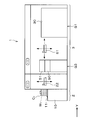
- the bonding apparatus 41 includes a processing container 100 that can seal the inside.
- the inside of the processing container 100 is partitioned by the inner wall 103 into a transport area T1 and a processing area T2.
- the loading / unloading port 101 described above is formed on the side surface of the processing container 100 in the transfer region T1.
- a loading / unloading port 104 for the wafers W U and W L and the overlapped wafer W T is formed on the inner wall 103.
- a transition 110 for temporarily placing the wafers W U and W L and the superposed wafer W T is provided on the Y direction positive direction side of the transfer region T1.
- the transition 110 is formed in, for example, two stages, and any two of the wafers W U , W L , and the superposed wafer W T can be placed at the same time.
- a wafer transfer mechanism 111 is provided in the transfer area T1. As shown in FIGS. 4 and 5, the wafer transfer mechanism 111 has a transfer arm 111 a that can move around, for example, the vertical direction, the horizontal direction (X direction, Y direction), and the vertical axis. Then, the wafer transfer mechanism 111 can transport within transfer region T1, or a transfer region T1 wafer W U between the processing region T2, W L, the overlapped wafer W T.
- a position adjusting mechanism 120 for adjusting the horizontal direction of the wafers W U and W L is provided on the Y direction negative direction side of the transfer region T1.
- the position adjustment mechanism 120 the position of the notches of the wafers W U and W L is detected by the detection unit 122 while rotating the wafers W U and W L held on the base 121.
- the horizontal direction of the wafers W U and W L is adjusted by adjusting the position.
- the structure for holding the wafers W U and W L on the base 121 is not particularly limited, and various structures such as a pin chuck structure and a spin chuck structure are used.
- Reversing mechanism 130 for reversing the front and rear surfaces of the upper wafer W U is provided.
- Reversing mechanism 130 has a holding arm 131 which holds the upper wafer W U.
- the holding arm 131 extends in the horizontal direction (X direction).
- the holding arm 131 is provided on the holding member 132 for holding the upper wafer W U, for example four positions.
- the holding arm 131 is supported by a driving unit 133 including, for example, a motor.
- a driving unit 133 including, for example, a motor.
- the holding arm 131 is rotatable around a horizontal axis.
- the holding arm 131 is rotatable about the drive unit 133 and is movable in the horizontal direction (X direction).
- Below the drive unit 133 for example, another drive unit (not shown) including a motor or the like is provided below the drive unit 133.
- this other driving unit the driving unit 133 can move in the vertical direction along the support pillar 134 extending in the vertical direction.
- Such driving unit 133, the upper wafer W U held by the holding member 132 is movable in the vertical direction and the horizontal direction together with the pivotable about a horizontal axis. Further, the upper wafer W U held by the holding member 132 can move around the drive unit 133 and move from the position adjustment mechanism 120 to the upper chuck 140 described later.
- the processing region T2 under the upper wafer W U and the chuck 140 as a first holding portion for holding suction on the lower surface, as a second holding portion for holding suction by placing the lower wafer W L with the upper surface
- a chuck 141 is provided.
- the lower chuck 141 is provided below the upper chuck 140 and is configured to be disposed so as to face the upper chuck 140. That is, the lower wafer W L held on the wafer W U and the lower chuck 141 on which is held by the upper chuck 140 is adapted to be placed opposite.
- the upper chuck 140 is held by an upper chuck rotating unit 150 provided above the upper chuck 140.
- the upper chuck rotating unit 150 is configured to rotate the upper chuck 140 around the vertical axis as will be described later. Further, the upper chuck rotating unit 150 is provided on the ceiling surface of the processing container 100.
- the upper chuck rotating portion 150 an upper imaging unit 151 to image the surface W L1 of the lower wafer W L held by the lower chuck 141 is provided. That is, the upper imaging unit 151 is provided adjacent to the upper chuck 140.
- the upper imaging unit 151 for example, a CCD camera is used.
- the lower chuck 141 is supported by a lower chuck stage 160 provided below the lower chuck 141.
- the lower chuck stage 160 is provided with a lower imaging unit 161 that images the surface W U1 of the upper wafer W U held by the upper chuck 140. That is, the lower imaging unit 161 is provided adjacent to the lower chuck 141.
- a CCD camera is used for the lower imaging unit 161 for the lower imaging unit 161, for example, a CCD camera is used.
- the lower chuck stage 160 is supported by a first lower chuck moving part 162 provided below the lower chuck stage 160, and the first lower chuck moving part 162 is further supported by a support base 163.
- the first lower chuck moving unit 162 is configured to move the lower chuck 141 in the horizontal direction (X direction) as described later.
- the first lower chuck moving part 162 is configured to be able to move the lower chuck 141 in the vertical direction.
- the support base 163 is provided on the lower surface side of the support base 163 and is attached to a pair of rails 164 and 164 extending in the horizontal direction (X direction).
- the support base 163 is configured to be movable along the rail 164 by the first lower chuck moving part 162.
- the first lower chuck moving part 162 is moved by, for example, a linear motor (not shown) provided along the rail 164.
- the pair of rails 164 and 164 are disposed in the second lower chuck moving portion 165.
- the second lower chuck moving unit 165 is provided on the lower surface side of the second lower chuck moving unit 165 and is attached to a pair of rails 166 and 166 extending in the horizontal direction (Y direction).
- the second lower chuck moving portion 165 is configured to be movable along the rail 166, that is, configured to move the lower chuck 141 in the horizontal direction (Y direction).
- the second lower chuck moving unit 165 moves by a linear motor (not shown) provided along the rail 166, for example.
- the pair of rails 166 and 166 are disposed on a mounting table 167 provided on the bottom surface of the processing container 100.
- the first lower chuck moving unit 162 and the second lower chuck moving unit 165 constitute the moving mechanism of the present invention.
- the upper chuck 140 employs a pin chuck system as shown in FIG.
- Upper chuck 140 includes a body portion 170 having a diameter larger than the diameter of the upper wafer W U in a plan view.
- a plurality of pins 171 that are in contact with the back surface W U2 of the upper wafer W U are provided on the lower surface of the main body 170.
- the outer ribs 172 for supporting the outer peripheral portion of the back surface W U2 of the upper wafer W U is provided on the outer peripheral portion of the back surface W U2 of the upper wafer W U is provided.
- the outer rib 172 is provided in an annular shape outside the plurality of pins 171.
- inner ribs 173 for supporting the back surface W U2 of the upper wafer W U is provided.
- the inner rib 173 is annularly provided concentrically with the outer rib 172.
- a region 174 inside the outer rib 172 (hereinafter sometimes referred to as a suction region 174) includes a first suction region 174a inside the inner rib 173 and a second suction region 174b outside the inner rib 173. It is divided into and.
- the first suction ports 175a are formed at, for example, four locations in the first suction region 174a.
- a first suction pipe 176a provided inside the main body 170 is connected to the first suction port 175a. Further, a first vacuum pump 177a is connected to the first suction pipe 176a.
- the second suction port 175b for evacuating the upper wafer W U is formed on the lower surface of the main body portion 170.
- the second suction port 175b is formed in two places in the second suction region 174b.
- a second suction pipe 176b provided inside the main body 170 is connected to the second suction port 175b.
- a second vacuum pump 177b is connected to the second suction pipe 176b.
- the suction regions 174a and 174b formed surrounded by the upper wafer W U , the main body 170 and the outer rib 172 are evacuated from the suction ports 175a and 175b, respectively, and the suction regions 174a and 174b are decompressed.
- the suction area 174a, for external atmosphere 174b is atmospheric pressure
- the upper wafer W U is sucked only by the atmospheric pressure correspondingly reduced in pressure areas 174a, pushed 174b side, top to upper chuck 140 wafer W U Is adsorbed and held.
- the upper chuck 140 is configured to be evacuated over the wafer W U per the first suction area 174a second suction region 174b.
- the outer rib 172 supports the outer peripheral portion of the back surface W U2 of the upper wafer W U, the upper wafer W U is suitably evacuated to the outer periphery thereof. Therefore, the entire surface of the upper wafer W U is held by suction on the chuck 140, to reduce the flatness of the on the wafer W U, it is possible to flatten the upper wafer W U.
- the height of the plurality of pins 171 is uniform, the flatness of the lower surface of the upper chuck 140 can be further reduced.
- the flat lower surface of the upper chuck 140 by reducing the lower surface flatness, it is possible to suppress the distortion of the vertical direction of the wafer W U after being held by the upper chuck 140.
- a through hole 178 that penetrates the main body 170 in the thickness direction is formed at the center of the main body 170.
- the central portion of the body portion 170 corresponds to the central portion of the upper wafer W U which is sucked and held on the chuck 140.
- tip part of the actuator part 191 in the pushing member 190 mentioned later penetrates the through-hole 178. As shown in FIG.
- the upper chuck rotating unit 150 includes an upper chuck stage 180 that is provided on the upper surface of the main body 170 of the upper chuck 140 and holds the upper chuck 140.
- the upper chuck stage 180 has an open top surface, has a hollow cylindrical shape, and has substantially the same shape as the main body 170 in plan view.
- a support member 181 that supports the upper chuck stage 180 and is attached to the ceiling surface of the processing container 100 is provided on the outer peripheral surface of the upper chuck stage 180.
- a slight gap is formed between the outer surface of the upper chuck stage 180 and the inner peripheral surface of the support member 181.
- the bottom surface an internal upper chuck stage 180, pressing member 190 for pressing the central portion of the upper wafer W U is further provided.
- the pushing member 190 has an actuator part 191 and a cylinder part 192.
- the actuator unit 191 generates a constant pressure in a fixed direction by air supplied from an electropneumatic regulator (not shown), and can generate the pressure constantly regardless of the position of the pressure application point. . Then, the air from the electropneumatic regulator, the actuator unit 191 is capable of controlling the pressing load applied against the central portion of the upper wafer W U and those in the center of the on the wafer W U. The tip of the actuator portion 191 is vertically movable through the through hole 178 by air from the electropneumatic regulator.
- the actuator part 191 is supported by the cylinder part 192.
- the cylinder part 192 can move the actuator part 191 in the vertical direction by a drive part incorporating a motor, for example.
- the pressing member 190 controls the pressing load by the actuator unit 191 and controls the movement of the actuator unit 191 by the cylinder unit 192. Then, the pressing member 190, the wafer W U to be described later, at the time of bonding of W L, it can be pressed by contacting the center portion of the center and lower wafer W L of the upper wafer W U.
- Rotating mechanism 200 for rotating upper chuck stage 180 (and upper chuck 140) is provided on support member 181 as shown in FIG.
- the rotation mechanism 200 is in contact with the outer peripheral surface of the upper chuck stage 180, and can rotate the upper chuck stage 180 by a drive unit incorporating a motor or the like, for example.
- the support member 181 is provided with a fixing portion 210 for fixing the upper chuck stage 180.
- the fixing portions 210 are provided at four locations at equal intervals on the outer peripheral surface of the upper chuck stage 180. Each fixing portion 210 blows air toward the outer peripheral surface of the upper chuck stage 180, thereby centering the upper chuck stage 180 and further fixing the upper chuck stage 180.
- the support member 181 is provided with linear scales 221 to 223 as position measuring units for measuring the position of the upper chuck stage 180, that is, the position of the upper chuck 140.
- the linear scales 221 to 223 respectively have scales 221a to 223a provided on the outer peripheral surface of the upper chuck stage 180, and detection heads 221b to 223b for reading the scales.
- a known method is used as a method for measuring the position of the upper chuck 140 using the linear scales 221 to 223.
- the first linear scale 221 is provided on the center line of the upper chuck stage 180 so as to face the rotation mechanism 200.
- the second linear scale 222 and the third linear scale 223 are provided at positions where the central angle formed by the first linear scale 221 is 90 degrees, and face each other on the center line of the upper chuck stage 180. Is provided. That is, the interval between the first linear scale 221 and the second linear scale 222 and the interval between the first linear scale 221 and the third linear scale 223 are equal.
- a linear scale is used as the position measurement unit, but the position measurement unit is not limited to this as long as the position of the upper chuck 140 is measured.
- a displacement meter may be used as the position measuring unit.
- the first linear scale 221 is connected to a servo amplifier (not shown), and the servo amplifier is connected to the control unit 70. That is, the first linear scale 221 is used for servo control (full-closed control), and the measurement result of the first linear scale 221 is the rotation direction ( ⁇ direction) around the vertical axis of the upper chuck 140 as described later. Used to adjust the position of
- the second linear scale 222 and the third linear scale 223 are each connected to the control unit 70.
- the measurement results of the three linear scales 221 to 223 are used to adjust the position of the upper chuck 140 in the horizontal direction (X direction and Y direction) as will be described later, and in some cases, the rotational direction of the upper chuck 140 ( This is used to adjust the position in the ⁇ direction.
- the eccentric amount (deviation amount) of the upper chuck 140 with respect to the lower chuck 141 is calculated from the measurement results of the three linear scales 221 to 223.
- FIG. 8 is an explanatory diagram showing dimensions when the eccentric amount of the upper chuck 140 is calculated.
- reference numeral 140 a is not eccentric, that is, a center point of the upper chuck 140 at a correct position
- 140 b indicates a center point of the eccentric upper chuck 140.
- the measurement results L1 to L3 of the three linear scales 221 to 223 are expressed by the following formulas (1) to (3), respectively.
- the measurement results L1 to L3 of the linear scales 221 to 223 are encoder values (absolute values) counted up clockwise.
- L1 y + R ⁇ (1)
- L2 ⁇ x + R ⁇ (2)
- L3 x + R ⁇ (3)
- Encoder value L2 of the second linear scale 222 Encoder value x of the third linear scale 223
- y Lower Eccentric amount of the upper chuck 140 relative to the chuck 141
- ⁇ Eccentric amount of the upper chuck 140 relative to the lower chuck 141 (rotational amount)
- R radius of the upper chuck 140
- the lower chuck 141 employs a pin chuck system as with the upper chuck 140.
- Lower chuck 141 includes a body portion 230 having a diameter larger than the diameter of the lower wafer W L in a plan view.
- the upper surface of the main body portion 230 a plurality of pins 231 in contact with the back surface W L2 of the lower wafer W L is provided.
- the outer ribs 232 for supporting the outer peripheral portion of the back surface W L2 of the lower wafer W L is provided.
- the outer rib 232 is annularly provided outside the plurality of pins 231.
- inner ribs 233 for supporting the back surface W L2 of the lower wafer W L is provided.
- the inner rib 233 is provided in an annular shape concentrically with the outer rib 232.
- the inner region 234 of the outer rib 232 (hereinafter sometimes referred to as a suction region 234) includes a first suction region 234a inside the inner rib 233 and a second suction region 234b outside the inner rib 233. It is divided into and.
- a first suction port 235a for evacuating the lower wafer W L are formed.
- the first suction port 235a is formed at one place in the first suction region 234a.
- a first suction pipe 236a provided inside the main body 230 is connected to the first suction port 235a.
- a first vacuum pump 237a is connected to the first suction pipe 236a.
- the second suction port 235b for evacuating the lower wafer W L are formed on the upper surface of the main body portion 230.
- the second suction port 235b is formed in two places in the second suction region 234b.
- a second suction tube 236b provided inside the main body 230 is connected to the second suction port 235b.
- a second vacuum pump 237b is connected to the second suction pipe 236b.
- the suction area 234a, for external atmosphere 234b is atmospheric pressure
- lower wafer W L suction area 234a only by atmospheric pressure correspondingly reduced in pressure, pressed 234b side lower wafer W L to lower chuck 141 Is adsorbed and held.
- the lower chuck 141 is evacuated configured to be able to lower wafer W L for each of the first suction area 234a second suction region 234b.
- the lower wafer W L is suitably evacuated to the outer periphery thereof. Therefore, the entire surface of the lower wafer W L is sucked and held on the lower chuck 141, to reduce the flatness of the lower wafer W L, it is possible to flatten the lower wafer W L.
- the height of the plurality of pins 231 is uniform, the flatness of the upper surface of the lower chuck 141 can be further reduced.
- the flat upper surface of the lower chuck 141 by reducing the flatness of the upper surface, it is possible to suppress distortion in the vertical direction of the lower wafer W L held by the lower chuck 141.
- the outer peripheral portion of the main body portion 230, the wafer W U, W L, or jump out from the overlapped wafer W T is lower chuck 141, a guide member to prevent the sliding (not shown) is provided.
- the guide members are provided at a plurality of positions, for example, at four positions at equal intervals on the outer peripheral portion of the main body 230.
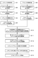
- FIG. 9 is a flowchart showing an example of main steps of the wafer bonding process.
- the cassette C U, the cassette C L accommodating the lower wafer W L of the plurality, and the empty cassette C T is a predetermined cassette mounting plate 11 of the carry-out station 2 accommodating the wafers W U on the plurality Placed on. Thereafter, the upper wafer W U in the cassette C U is taken out by the wafer transfer device 22 is conveyed to the transition unit 50 of the third processing block G3 in the processing station 3.
- the upper wafer W U is transferred to the surface modification apparatus 30 of the first processing block G1 by the wafer transfer apparatus 61.
- oxygen gas or nitrogen gas which is a processing gas, is excited and turned into plasma and ionized under a predetermined reduced-pressure atmosphere.
- the surface W U1 of the upper wafer W U is irradiated with this oxygen ion or nitrogen ion, and the surface W U1 is subjected to plasma treatment.
- the surface W U1 of the upper wafer W U is modified (Step S1 in FIG. 9).
- the upper wafer W U is transferred to a surface hydrophilizing apparatus 40 of the second processing block G2 by the wafer transfer apparatus 61.
- the surface hydrophilizing device 40 while rotating the upper wafer W U held by the spin chuck, for supplying pure water onto the onto the wafer W U. Then, the supplied pure water is diffused over the front surface W U1 of the upper wafer W U, the surface W U1 to hydroxyl (silanol group) in the upper wafer W U which are modified in the surface modification apparatus 30 is the attached The surface W U1 is hydrophilized. Further, the surface W U1 of the upper wafer W U is cleaned with the pure water (step S2 in FIG. 9).
- the upper wafer W U is transferred to the bonding apparatus 41 of the second processing block G2 by the wafer transfer apparatus 61.
- Upper wafer W U which is carried into the joining device 41 is conveyed to the position adjusting mechanism 120 by the wafer transfer mechanism 111 via the transition 110.
- the position adjusting mechanism 120, the horizontal orientation of the upper wafer W U is adjusted (step S3 in FIG. 9).
- the upper wafer W U is transferred from the position adjusting mechanism 120 to the holding arm 131 of the reversing mechanism 130. Subsequently, in transfer region T1, by reversing the holding arm 131, the front and back surfaces of the upper wafer W U is inverted (step S4 in FIG. 9). That is, the surface W U1 of the upper wafer W U is directed downward.
- the holding arm 131 of the reversing mechanism 130 rotates around the driving unit 133 and moves below the upper chuck 140.
- the upper wafer W U is delivered from the reversing mechanism 130 to the upper chuck 140.
- Upper wafer W U, the back surface W U2 above the chuck 140 is held by suction (step S5 in FIG. 9).
- the vacuum pump 177a actuates the 177b, the suction area 174a, the upper wafer W U evacuated suction port 175a, via 175b in 174b, the upper wafer W U is attracted and held on the chuck 140 .
- the processing of the lower wafer W L Following the on wafer W U is performed.
- the lower wafer W L in the cassette C L is taken out by the wafer transfer device 22 is conveyed to the transition unit 50 in the processing station 3.
- Step S6 In FIG. 9
- modification of the surface W L1 of the lower wafer W L in step S6 is the same as step S1 of the aforementioned.
- step S7 hydrophilic and cleaning of the surface W L1 of the lower wafer W L in step S7, is similar to the process S2 described above.
- the lower wafer W L is transported to the bonding apparatus 41 by the wafer transfer apparatus 61.
- Lower wafer W L which is transported to the bonding unit 41 is conveyed to the position adjusting mechanism 120 by the wafer transfer mechanism 111 via the transition 110.
- the position adjusting mechanism 120, the horizontal orientation of the lower wafer W L are adjusted (step S8 in FIG. 9).
- the lower wafer W L is transferred to the lower chuck 141 by the wafer transfer mechanism 111, the back surface W L2 is held by suction to the lower chuck 141 (step S9 in FIG. 9).
- the vacuum pump 237a actuates the 237b, evacuated, and the lower wafer W L is sucked and held by the lower chuck 141 to the lower wafer W L through the suction port 235a, 235b suction area 234a, in 234b .
- the upper image capturing section 151 and the lower imaging unit 161 performs an initial adjustment of the rotational position of the upper wafer W U and the lower wafer W L (horizontal orientation).
- the lower chuck 141 is moved in the horizontal direction (X direction and Y direction) by the first lower chuck moving unit 162 and the second lower chuck moving unit 165, and the lower wafer is used by using the upper imaging unit 151.
- a predetermined reference point for example, two points on the outer peripheral portion
- a predetermined reference point for example, two points on the outer peripheral portion
- a predetermined reference point for example, two points on the outer peripheral portion
- the surface W U1 of the upper wafer W U is sequentially imaged using the lower imaging unit 161.
- the captured image is output to the control unit 70.
- the control unit 70 such as based on the image captured by the image and the lower image pickup unit 161 captured by the upper imaging unit 151, the reference point of the reference point and the lower wafer W L of the upper wafer W U matches each position , that is, the direction of the upper wafer W U and the lower wafer W L in a position to match, rotate the upper chuck 140 by a rotating mechanism 200.
- the rotational position of the upper wafer W U and the lower wafer W L is initially adjusted (step S10 in FIG. 9).
- step S11 a first rotational position of the upper chuck 140 using the linear scale 221 is to be adjusted, the first in the linear scale 221, the wafer on which is held by the upper chuck 140 W U and the lower chuck You can not grasp the initial state of the rotating direction of the lower wafer W L held in the 141. Therefore, in the step S10 described above, the rotational direction position of the upper wafer W U and the lower wafer W L is initially adjusted.
- step S10 the position of the upper chuck 140 is measured using the first linear scale 221.
- the measurement result of the first linear scale 221, that is, the encoder value L 1 of the first linear scale 221 is output to the control unit 70.
- the rotational direction eccentricity ⁇ of the upper chuck 140 relative to the lower chuck 141 is within a predetermined threshold, for example, ⁇ 0.2 [ ⁇ rad].
- a correction amount in the rotation direction of the upper chuck 140 is calculated, and the rotation mechanism 200 is controlled. Then, the rotational direction position of the upper chuck 140 relative to the lower chuck 141 is adjusted by the rotation mechanism 200 rotating the upper chuck 140 by the correction amount (step S11 in FIG. 9).
- step S11 the first linear scale 221 located farthest from the rotation mechanism 200 is used.
- the encoder value L2 of the second linear scale 222 or the encoder value L3 of the third linear scale 223 is compared with the encoder value L3 of the first linear scale 221.
- the encoder value L1 is greatly affected by the deviation. Therefore, the rotational direction position of the upper chuck 140 can be adjusted more appropriately.
- step S11 when the upper chuck 140 is rotated by the rotation mechanism 200, the upper chuck stage 180 is centered by the fixing unit 210.
- step S11 the rotation mechanism 200 may be controlled so that the rotational direction eccentricity ⁇ of the upper chuck 140 becomes zero. Further, when the encoder value L1 of the first linear scale 221 is within a predetermined threshold as a result of the measurement by the first linear scale 221, it is not necessary to rotate the upper chuck 140 by the rotating mechanism 200.
- the center point (rotation axis) of the upper chuck 140 may be shifted in the horizontal direction from 140a to 140b as shown in FIG.
- the center point of the upper chuck 140 is shifted in the horizontal direction.
- the upper chuck 140 is centered by the air from the four fixing portions 210. However, depending on the air balance from these fixing portions 210, the center point of the upper chuck 140 is shifted in the horizontal direction.
- the horizontal direction (X direction and Y direction) of the upper chuck 140 is adjusted so that the X direction eccentricity x of the upper chuck 140 and the Y direction eccentricity y of the upper chuck 140 are within a predetermined threshold, for example, 1 ⁇ m.
- the first lower chuck moving part 162 and the second lower chuck moving part 165 are controlled.
- the upper chuck 140 with respect to the lower chuck 141 is moved by the correction amount in the horizontal direction (X direction and Y direction) by the first lower chuck moving unit 162 and the second lower chuck moving unit 165. Is adjusted (step S12 in FIG. 9).
- step S12 the interval between the first linear scale 221 and the second linear scale 222 and the interval between the first linear scale 221 and the third linear scale 223 are equal, so that the above (4) to (6) A simple formula can be used.
- the equation for calculating the amount of eccentricity of the upper chuck 140 becomes complicated, and the control thereof becomes complicated. Therefore, in the present embodiment, the horizontal position of the upper chuck 140 can be adjusted with simple control.
- step S12 the first lower chuck moving unit 162 and the second lower chuck moving unit 165 are controlled so that the X direction eccentric amount x and the Y direction eccentric amount y of the upper chuck 140 become zero. But of course.
- the encoder values L1 to L3 of the linear scales 221 to 223 are within predetermined thresholds as a result of measurement by the three linear scales 221 to 223, the first lower chuck moving unit 162 and the second lower chuck moving unit 162 It is not necessary to move the upper chuck 140 to the horizontal treasury by the lower chuck moving unit 165.
- step S12 of the present embodiment the horizontal position of the upper chuck 140 is adjusted.
- the rotational direction eccentricity ⁇ of the upper chuck 140 calculated by the above formula (6) is within a predetermined threshold, for example ⁇ If not 0.2 [ ⁇ rad], the rotational position of the upper chuck 140 may be further adjusted.
- the control unit 70 calculates a correction amount in the rotation direction of the upper chuck 140 based on the rotation direction eccentricity ⁇ of the upper chuck 140.
- the rotation mechanism 200 rotates the upper chuck 140 by the correction amount, so that the rotational direction position of the upper chuck 140 with respect to the lower chuck 141 is adjusted.
- the first lower chuck moving unit 162 moves the lower chuck 141 vertically upward to adjust the vertical position of the upper chuck 140 and the lower chuck 141, and the upper wafer W U held by the upper chuck 140 is adjusted.
- performing adjustment of vertical position of the lower wafer W L held by the lower chuck 141 (the step S13 in FIG. 9).
- the upper wafer W U and the lower wafer W L is opposed to a predetermined position.
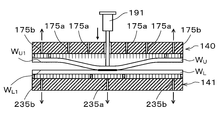
- the actuator portion 191 is lowered by the cylinder portion 192 of the pushing member 190. Then, with the downward movement of the actuator portion 191, the center portion of the upper wafer W U is lowered is pressed. At this time, a predetermined pressing load is applied to the actuator unit 191 by the air supplied from the electropneumatic regulator. Then, the pressing member 190 is pressed by abutting the central portion of the central portion and the lower wafer W L of the upper wafer W U (step S14 in FIG. 9).
- a second vacuum pump 177b is The second suction region 174b is evacuated from the second suction port 175b while being operated. Then, even when pressing the central portion of the upper wafer W U by the pressing member 190 can hold the outer peripheral portion of the upper wafer W U by the upper chuck 140.
- the bonding is started between the central portion of the central portion and the lower wafer W L of the upper wafer W U which pressed (thick line portion in FIG. 10). That is, since the surface W U1 of the upper wafer W U and the surface W L1 of the lower wafer W L are modified in steps S1 and S6, respectively, first, the van der Waals force (intermolecular) between the surfaces W U1 and W L1. Force) is generated, and the surfaces W U1 and W L1 are joined to each other.
- the pressing member 190 of the upper wafer W U in a state where the center portion is pressed in the center and lower wafer W L to stop the operation of the second vacuum pump 177b, the second in the second suction region 174b stopping evacuation of the upper wafer W U from the suction port 175b.
- the upper wafer W U falls onto the lower wafer W L.
- the upper wafer W U sequentially falls and comes into contact with the lower wafer W L , and the above-described bonding by the van der Waals force and hydrogen bonding between the surfaces W U1 and W L1 is sequentially expanded.
- the surface W L1 of the surface W U1 and the lower wafer W L of the upper wafer W U abuts on the whole surface, the upper wafer W U and the lower wafer W L is bonded (step S15 in FIG. 9).
- step S15 since the back surface W U2 of the upper wafer W U is supported by a plurality of pins 171, when releasing the vacuum of the upper wafer W U by the upper chuck 140, the upper the on wafer W U chuck 140 It is easy to peel off. Therefore, expansion of the bonding of the upper wafer W U and the lower wafer W L (bonding wave) is a true circle, the upper wafer W U and the lower wafer W L are suitably joined.
- the actuator portion 191 of the pushing member 190 is raised to the upper chuck 140. Further, the vacuum pump 237a, and stops the operation of 237b, to stop the evacuation of the lower wafer W L in the suction region 234, stopping the suction and holding of the lower wafer W L by the lower chuck 141. At this time, since the back surface W L2 of the lower wafer W L is supported by a plurality of pins 231, when releasing the vacuum of the lower wafer W L by the lower chuck 141, peeling the under wafer W L from the lower chuck 141 It is easy.
- the upper wafer W U and the lower wafer W L overlapped wafer bonded W T is transferred to the transition unit 51 by the wafer transfer apparatus 61, then carry out by the wafer transfer apparatus 22 of the station 2 of a predetermined cassette mounting plate 11 It is conveyed to the cassette C T.
- a series of wafers W U, bonding process of W L is completed.
- the rotational direction position of the upper chuck 140 relative to the lower chuck 141 is adjusted using the measurement result of the first linear scale 221.
- the first linear scale 221 that is farthest from the rotation mechanism 200 the upper chuck 140 and the lower chuck 141 are more appropriately displaced in the rotation direction than when the other linear scales 222 and 223 are used.
- the position of the upper chuck 140 in the rotational direction can be adjusted appropriately.
- step S12 the horizontal position of the upper chuck 140 relative to the lower chuck 141 is adjusted using the measurement results of the three linear scales 221 to 223. Therefore, even when the horizontal position of the upper chuck 140 is shifted when adjusting the rotational position of the upper chuck 140 in step S11, the horizontal position of the upper chuck 140 is corrected and adjusted appropriately in step S12. can do.
- step S12 when the rotational direction eccentricity ⁇ of the upper chuck 140 is not within a predetermined threshold, the rotational direction position of the upper chuck 140 can be adjusted appropriately.
- step S11, S12 as described above hold it is possible to adjust the relative position of the upper chuck 140 and lower chuck 141 properly, the wafer W U and the lower chuck 141 on which is held on the on the chuck 140 by bonding process of the lower wafer W L has can be appropriately performed.
- the bonding system 1 of the present embodiment includes the surface modification device 30, the surface hydrophilization device 40, and the bonding device 41, the bonding of the wafers W U and W L can be efficiently performed in one system. It can be carried out. Therefore, the throughput of the wafer bonding process can be further improved.
- the second linear scale 222 and the third linear scale 223 are provided at positions where the central angle formed by the first linear scale 221 is 90 degrees, and the upper chuck Although they are provided opposite to each other on the center line of the stage 180, the arrangement of the second linear scale 222 and the third linear scale 223 is not limited to this.
- the interval between the first linear scale 221 and the second linear scale 222 and the interval between the first linear scale 221 and the third linear scale 223 are equal.
- the center angle formed by the first linear scale 221 may be provided at a position different from 90 degrees, for example, 45 degrees.
- the amount of eccentricity of the upper chuck 140 can be calculated using a simple expression such as the above expressions (4) to (6).
- the position of the upper chuck 140 can be adjusted with simple control.
- the upper chuck 140 is configured to be rotatable, but the lower chuck 141 may be configured to be rotatable.
- the three linear scales 221 to 223 are provided on the lower chuck 141.
- both the upper chuck 140 and the lower chuck 141 may be configured to be rotatable.
- the three linear scales 221 to 223 are provided in either the upper chuck 140 or the lower chuck 141.
- the lower chuck 141 is configured to be movable in the horizontal direction.
- the upper chuck 140 may be configured to be movable in the horizontal direction, or the upper chuck 140 may be configured to move in the horizontal direction.
- Both the lower chuck 141 and the lower chuck 141 may be configured to be movable in the horizontal direction.
- the lower chuck 141 is configured to be movable in the vertical direction, but the upper chuck 140 may be configured to be movable in the vertical direction, or both the upper chuck 140 and the lower chuck 141 are moved in the vertical direction. You may comprise.
- the wafer W U by bonding device 41 after joining the W L, may be further heated bonded overlapped wafer W T with a predetermined temperature (annealing) .
- annealing a predetermined temperature
- the present invention is not limited to such examples. It is obvious for those skilled in the art that various changes or modifications can be conceived within the scope of the idea described in the claims, and these are naturally within the technical scope of the present invention. It is understood.
- the present invention is not limited to this example and can take various forms.
- the present invention can also be applied to a case where the substrate is another substrate such as an FPD (flat panel display) other than a wafer or a mask reticle for a photomask.
- FPD flat panel display
Landscapes
- Engineering & Computer Science (AREA)
- Mechanical Engineering (AREA)
- Container, Conveyance, Adherence, Positioning, Of Wafer (AREA)
- Wire Bonding (AREA)
- Manufacturing & Machinery (AREA)
- Pressure Welding/Diffusion-Bonding (AREA)
Abstract
Description
本願は、2016年11月9日に日本国に出願された特願2016-218579号に基づき、優先権を主張し、その内容をここに援用する。
先ず、本実施の形態にかかる接合システムの構成について説明する。図1は、接合システム1の構成の概略を示す平面図である。図2は、接合システム1の内部構成の概略を示す側面図である。
次に、上述した接合装置41の構成について説明する。
接合装置41は、図4に示すように内部を密閉可能な処理容器100を有している。処理容器100のウェハ搬送領域60側の側面には、ウェハWU、WL、重合ウェハWTの搬入出口101が形成され、当該搬入出口101には開閉シャッタ102が設けられている。
次に、接合装置41の上チャック140と上チャック回転部150の詳細な構成について説明する。
第1のリニアスケール221はサーボアンプ(図示せず)に接続され、さらにサーボアンプは制御部70に接続されている。すなわち、第1のリニアスケール221はサーボ制御(フルクローズ制御)に用いられ、当該第1のリニアスケール221の測定結果は、後述するように上チャック140の鉛直軸回りの回転方向(θ方向)の位置を調節するために用いられる。
L1=y+Rθ ・・・(1)
L2=-x+Rθ ・・・(2)
L3=x+Rθ ・・・(3)
但し、
L1:第1のリニアスケール221のエンコーダ値
L2:第2のリニアスケール222のエンコーダ値
L3:第3のリニアスケール223のエンコーダ値
x:下チャック141に対する上チャック140のX方向偏心量
y:下チャック141に対する上チャック140のY方向偏心量
θ:下チャック141に対する上チャック140の回転方向偏心量(回転量)
R:上チャック140の半径
x=(L3-L2)/2 ・・・(4)
y=L1-(L3+L2)/2 ・・・(5)
θ=(L3+L2)/2R ・・・(6)
次に、接合装置41の下チャック141の詳細な構成について説明する。
次に、以上のように構成された接合システム1を用いて行われるウェハWU、WLの接合処理方法について説明する。図9は、かかるウェハ接合処理の主な工程の例を示すフローチャートである。
x=(L3-L2)/2 ・・・(4)
y=L1-(L3+L2)/2 ・・・(5)
θ=(L3+L2)/2R ・・・(6)
次に、本発明の他の実施の形態について説明する。
2 搬入出ステーション
3 処理ステーション
30 表面改質装置
40 表面親水化装置
41 接合装置
61 ウェハ搬送装置
70 制御部
140 上チャック
141 下チャック
150 上チャック回転部
162 第1の下チャック移動部
165 第2の下チャック移動部
200 回転機構
221 第1のリニアスケール
222 第2のリニアスケール
223 第3のリニアスケール
WU 上ウェハ
WL 下ウェハ
WT 重合ウェハ
Claims (12)
- 基板同士を接合する接合装置であって、
下面に第1の基板を真空引きして吸着保持する第1の保持部と、
前記第1の保持部の下方に設けられ、上面に第2の基板を真空引きして吸着保持する第2の保持部と、
前記第1の保持部と前記第2の保持部を相対的に回転させる回転機構と、
前記第1の保持部と前記第2の保持部を相対的に水平方向に移動させる移動機構と、
前記回転機構によって回転する前記第1の保持部又は前記第2の保持部に設けられ、当該第1の保持部又は第2の保持部の位置を測定する3つの位置測定部と、
前記3つの位置測定部による測定結果に基づいて、前記回転機構と前記移動機構を制御する制御部と、を有する、接合装置。 - 請求項1に記載の接合装置において、
前記制御部は、前記3つの位置測定部のうち第1の位置測定部による測定結果に基づいて、前記回転機構を制御した後、前記3つの位置測定部の測定結果に基づいて、前記移動機構を制御するように構成されている。 - 請求項1に記載の接合装置において、
前記制御部は、前記3つの位置測定部のうち第1の位置測定部による測定結果に基づいて、前記回転機構を制御した後、前記3つの位置測定部の測定結果に基づいて、前記回転機構と前記移動機構を制御するように構成されている。 - 請求項2に記載の接合装置において、
前記回転機構は、前記第1の保持部の外周部又は前記第2の保持部の外周部に設けられ、
前記第1の位置測定部は、前記回転機構が設けられた前記第1の保持部の外周部又は前記第2の保持部の外周部において、当該第1の保持部又は第2の保持部の中心線上に前記回転機構に対向して設けられている。 - 請求項2に記載の接合装置において、
前記第1の位置測定部と第2の位置測定部の間隔と、前記第1の位置測定部と第3の位置測定部の間隔は等しい。 - 基板同士を接合する接合装置を備えた接合システムであって、
前記接合装置は、
下面に第1の基板を真空引きして吸着保持する第1の保持部と、
前記第1の保持部の下方に設けられ、上面に第2の基板を真空引きして吸着保持する第2の保持部と、
前記第1の保持部と前記第2の保持部を相対的に回転させる回転機構と、
前記第1の保持部と前記第2の保持部を相対的に水平方向に移動させる移動機構と、
前記回転機構によって回転する前記第1の保持部又は前記第2の保持部に設けられ、当該第1の保持部又は第2の保持部の位置を測定する3つの位置測定部と、
前記3つの位置測定部による測定結果に基づいて、前記回転機構と前記移動機構を制御する制御部と、を有し、
前記接合システムは、
前記接合装置を備えた処理ステーションと、
第1の基板、第2の基板又は第1の基板と第2の基板が接合された重合基板をそれぞれ複数保有可能で、且つ前記処理ステーションに対して第1の基板、第2の基板又は重合基板を搬入出する搬入出ステーションと、を備え、
前記処理ステーションは、
第1の基板又は第2の基板の接合される表面を改質する表面改質装置と、
前記表面改質装置で改質された第1の基板又は第2の基板の表面を親水化する表面親水化装置と、
前記表面改質装置、前記表面親水化装置及び前記接合装置に対して、第1の基板、第2の基板又は重合基板を搬送するための搬送装置と、を有し、
前記接合装置では、前記表面親水化装置で表面が親水化された第1の基板と第2の基板を接合する。 - 接合装置を用いて基板同士を接合する接合方法であって、
前記接合装置は、
下面に第1の基板を真空引きして吸着保持する第1の保持部と、
前記第1の保持部の下方に設けられ、上面に第2の基板を真空引きして吸着保持する第2の保持部と、
前記第1の保持部と前記第2の保持部を相対的に回転させる回転機構と、
前記第1の保持部と前記第2の保持部を相対的に水平方向に移動させる移動機構と、
前記回転機構によって回転する前記第1の保持部又は前記第2の保持部に設けられ、当該第1の保持部又は第2の保持部の位置を測定する3つの位置測定部と、を有し、
前記接合方法は、
前記3つの位置測定部を用いて、前記第1の保持部又は前記第2の保持部の位置を測定する測定工程と、
前記測定工程における測定結果に基づいて、前記前記回転機構と前記移動機構を制御し、前記第1の保持部と前記第2の保持部の相対的な位置を調節する位置調節工程と、を有する。 - 請求項7に記載の接合方法において、
前記3つの位置測定部のうち第1の位置測定部を用いて、前記第1の保持部又は前記第2の保持部の位置を測定する第1の測定工程と、
前記第1の測定工程における測定結果に基づいて、前記回転機構を制御し、前記第1の保持部と前記第2の保持部の相対的な位置を調節する第1の位置調節工程と、
その後、前記3つの位置測定部を用いて、前記第1の保持部又は前記第2の保持部の位置を測定する第2の測定工程と、
前記第2の測定工程における測定結果に基づいて、前記移動機構を制御し、前記第1の保持部と前記第2の保持部の相対的な位置を調節する第2の位置調節工程と、を有する。 - 請求項7に記載の接合方法において、
前記3つの位置測定部のうち第1の位置測定部を用いて、前記第1の保持部又は前記第2の保持部の位置を測定する第1の測定工程と、
前記第1の測定工程における測定結果に基づいて、前記回転機構を制御し、前記第1の保持部と前記第2の保持部の相対的な位置を調節する第1の位置調節工程と、
その後、前記3つの位置測定部を用いて、前記第1の保持部又は前記第2の保持部の位置を測定する第2の測定工程と、
前記第2の測定工程における測定結果に基づいて、前記回転機構と前記移動機構を制御し、前記第1の保持部と前記第2の保持部の相対的な位置を調節する第2の位置調節工程と、を有する。 - 請求項8に記載の接合方法において、
前記回転機構は、前記第1の保持部の外周部又は前記第2の保持部の外周部に設けられ、
前記第1の位置測定部は、前記回転機構が設けられた前記第1の保持部の外周部又は前記第2の保持部の外周部において、当該第1の保持部又は第2の保持部の中心線上に前記回転機構に対向して設けられている。 - 請求項8に記載の接合方法において、
前記第1の位置測定部と第2の位置測定部の間隔と、前記第1の位置測定部と第3の位置測定部の間隔は等しい。 - 接合方法を接合装置によって実行させるように、当該接合装置を制御する制御部のコンピュータ上で動作するプログラムを格納した読み取り可能なコンピュータ記憶媒体であって、
前記接合装置は、
下面に第1の基板を真空引きして吸着保持する第1の保持部と、
前記第1の保持部の下方に設けられ、上面に第2の基板を真空引きして吸着保持する第2の保持部と、
前記第1の保持部と前記第2の保持部を相対的に回転させる回転機構と、
前記第1の保持部と前記第2の保持部を相対的に水平方向に移動させる移動機構と、
前記回転機構によって回転する前記第1の保持部又は前記第2の保持部に設けられ、当該第1の保持部又は第2の保持部の位置を測定する3つの位置測定部と、を有し、
前記接合方法は、
前記3つの位置測定部を用いて、前記第1の保持部又は前記第2の保持部の位置を測定する測定工程と、
前記測定工程における測定結果に基づいて、前記前記回転機構と前記移動機構を制御し、前記第1の保持部と前記第2の保持部の相対的な位置を調節する位置調節工程と、を有する。
Priority Applications (6)
| Application Number | Priority Date | Filing Date | Title |
|---|---|---|---|
| JP2018550075A JP6703619B2 (ja) | 2016-11-09 | 2017-10-10 | 接合装置、接合システム、接合方法及びコンピュータ記憶媒体 |
| KR1020227002444A KR102416773B1 (ko) | 2016-11-09 | 2017-10-10 | 접합 장치, 접합 시스템, 접합 방법 및 컴퓨터 기억 매체 |
| CN201780069249.XA CN109923639B (zh) | 2016-11-09 | 2017-10-10 | 接合装置、接合系统、接合方法和计算机存储介质 |
| KR1020197012912A KR102356109B1 (ko) | 2016-11-09 | 2017-10-10 | 접합 장치, 접합 시스템, 접합 방법 및 컴퓨터 기억 매체 |
| US16/347,856 US11094667B2 (en) | 2016-11-09 | 2017-10-10 | Bonding apparatus, bonding system, bonding method, and recording medium |
| US17/374,156 US11658146B2 (en) | 2016-11-09 | 2021-07-13 | Bonding apparatus, bonding system, bonding method, and recording medium |
Applications Claiming Priority (2)
| Application Number | Priority Date | Filing Date | Title |
|---|---|---|---|
| JP2016-218579 | 2016-11-09 | ||
| JP2016218579 | 2016-11-09 |
Related Child Applications (2)
| Application Number | Title | Priority Date | Filing Date |
|---|---|---|---|
| US16/347,856 A-371-Of-International US11094667B2 (en) | 2016-11-09 | 2017-10-10 | Bonding apparatus, bonding system, bonding method, and recording medium |
| US17/374,156 Continuation US11658146B2 (en) | 2016-11-09 | 2021-07-13 | Bonding apparatus, bonding system, bonding method, and recording medium |
Publications (1)
| Publication Number | Publication Date |
|---|---|
| WO2018088091A1 true WO2018088091A1 (ja) | 2018-05-17 |
Family
ID=62110433
Family Applications (1)
| Application Number | Title | Priority Date | Filing Date |
|---|---|---|---|
| PCT/JP2017/036657 Ceased WO2018088091A1 (ja) | 2016-11-09 | 2017-10-10 | 接合装置、接合システム、接合方法及びコンピュータ記憶媒体 |
Country Status (5)
| Country | Link |
|---|---|
| US (2) | US11094667B2 (ja) |
| JP (2) | JP6703619B2 (ja) |
| KR (2) | KR102416773B1 (ja) |
| CN (1) | CN109923639B (ja) |
| WO (1) | WO2018088091A1 (ja) |
Cited By (2)
| Publication number | Priority date | Publication date | Assignee | Title |
|---|---|---|---|---|
| JP2021125660A (ja) * | 2020-02-10 | 2021-08-30 | 東京エレクトロン株式会社 | 基板位置決め装置、基板位置決め方法および接合装置 |
| JP2023154157A (ja) * | 2022-04-06 | 2023-10-19 | 東京エレクトロン株式会社 | 接合装置、接合システム、接合方法および記憶媒体 |
Families Citing this family (3)
| Publication number | Priority date | Publication date | Assignee | Title |
|---|---|---|---|---|
| KR102416773B1 (ko) * | 2016-11-09 | 2022-07-05 | 도쿄엘렉트론가부시키가이샤 | 접합 장치, 접합 시스템, 접합 방법 및 컴퓨터 기억 매체 |
| CN112038220B (zh) * | 2020-08-31 | 2023-02-03 | 上海华力集成电路制造有限公司 | 晶圆键合工艺中改善晶圆边缘形变的方法 |
| US12500108B2 (en) * | 2023-08-08 | 2025-12-16 | Taiwan Semiconductor Manufacturing Company, Ltd. | Bonding system and method |
Citations (2)
| Publication number | Priority date | Publication date | Assignee | Title |
|---|---|---|---|---|
| JP2009200117A (ja) * | 2008-02-19 | 2009-09-03 | Nikon Corp | 接合装置および製造方法 |
| JP2015018919A (ja) * | 2013-07-10 | 2015-01-29 | 東京エレクトロン株式会社 | 接合装置、接合システム、接合方法、プログラム及びコンピュータ記憶媒体 |
Family Cites Families (10)
| Publication number | Priority date | Publication date | Assignee | Title |
|---|---|---|---|---|
| JP5090725B2 (ja) * | 2006-12-20 | 2012-12-05 | 株式会社日立ハイテクノロジーズ | 異物検査装置 |
| JP5732631B2 (ja) * | 2009-09-18 | 2015-06-10 | ボンドテック株式会社 | 接合装置および接合方法 |
| JP5421825B2 (ja) * | 2010-03-09 | 2014-02-19 | 東京エレクトロン株式会社 | 接合システム、接合方法、プログラム及びコンピュータ記憶媒体 |
| JP5490741B2 (ja) * | 2011-03-02 | 2014-05-14 | 東京エレクトロン株式会社 | 基板搬送装置の位置調整方法、及び基板処理装置 |
| WO2014064944A1 (ja) * | 2012-10-26 | 2014-05-01 | 株式会社ニコン | 基板貼り合わせ装置、位置合わせ装置、基板貼り合わせ方法、位置合わせ方法、及び、積層半導体装置の製造方法 |
| JP6501447B2 (ja) * | 2013-03-26 | 2019-04-17 | 芝浦メカトロニクス株式会社 | 貼合装置および貼合基板の製造方法 |
| JP2015119088A (ja) * | 2013-12-19 | 2015-06-25 | 東京エレクトロン株式会社 | 接合方法、プログラム、コンピュータ記憶媒体、接合装置及び接合システム |
| JP6271404B2 (ja) * | 2014-11-27 | 2018-01-31 | 東京エレクトロン株式会社 | 接合方法、プログラム、コンピュータ記憶媒体、接合装置及び接合システム |
| JP6049820B1 (ja) * | 2015-07-24 | 2016-12-21 | 信越エンジニアリング株式会社 | 貼合デバイスの製造装置及び製造方法 |
| KR102416773B1 (ko) * | 2016-11-09 | 2022-07-05 | 도쿄엘렉트론가부시키가이샤 | 접합 장치, 접합 시스템, 접합 방법 및 컴퓨터 기억 매체 |
-
2017
- 2017-10-10 KR KR1020227002444A patent/KR102416773B1/ko active Active
- 2017-10-10 WO PCT/JP2017/036657 patent/WO2018088091A1/ja not_active Ceased
- 2017-10-10 CN CN201780069249.XA patent/CN109923639B/zh active Active
- 2017-10-10 JP JP2018550075A patent/JP6703619B2/ja active Active
- 2017-10-10 KR KR1020197012912A patent/KR102356109B1/ko active Active
- 2017-10-10 US US16/347,856 patent/US11094667B2/en active Active
-
2020
- 2020-05-08 JP JP2020082757A patent/JP6883690B2/ja active Active
-
2021
- 2021-07-13 US US17/374,156 patent/US11658146B2/en active Active
Patent Citations (2)
| Publication number | Priority date | Publication date | Assignee | Title |
|---|---|---|---|---|
| JP2009200117A (ja) * | 2008-02-19 | 2009-09-03 | Nikon Corp | 接合装置および製造方法 |
| JP2015018919A (ja) * | 2013-07-10 | 2015-01-29 | 東京エレクトロン株式会社 | 接合装置、接合システム、接合方法、プログラム及びコンピュータ記憶媒体 |
Cited By (5)
| Publication number | Priority date | Publication date | Assignee | Title |
|---|---|---|---|---|
| JP2021125660A (ja) * | 2020-02-10 | 2021-08-30 | 東京エレクトロン株式会社 | 基板位置決め装置、基板位置決め方法および接合装置 |
| JP7370271B2 (ja) | 2020-02-10 | 2023-10-27 | 東京エレクトロン株式会社 | 基板位置決め装置、基板位置決め方法および接合装置 |
| TWI883110B (zh) * | 2020-02-10 | 2025-05-11 | 日商東京威力科創股份有限公司 | 基板定位裝置、基板定位方法及接合裝置 |
| JP2023154157A (ja) * | 2022-04-06 | 2023-10-19 | 東京エレクトロン株式会社 | 接合装置、接合システム、接合方法および記憶媒体 |
| JP7843636B2 (ja) | 2022-04-06 | 2026-04-10 | 東京エレクトロン株式会社 | 接合装置、接合システム、接合方法および記憶媒体 |
Also Published As
| Publication number | Publication date |
|---|---|
| US20190312006A1 (en) | 2019-10-10 |
| JP6883690B2 (ja) | 2021-06-09 |
| JPWO2018088091A1 (ja) | 2019-09-26 |
| US11658146B2 (en) | 2023-05-23 |
| JP2020127046A (ja) | 2020-08-20 |
| US20210343678A1 (en) | 2021-11-04 |
| US11094667B2 (en) | 2021-08-17 |
| KR102356109B1 (ko) | 2022-02-03 |
| CN109923639A (zh) | 2019-06-21 |
| KR20220017510A (ko) | 2022-02-11 |
| KR102416773B1 (ko) | 2022-07-05 |
| CN109923639B (zh) | 2023-07-21 |
| KR20190075947A (ko) | 2019-07-01 |
| JP6703619B2 (ja) | 2020-06-03 |
Similar Documents
| Publication | Publication Date | Title |
|---|---|---|
| KR102651554B1 (ko) | 접합 장치, 접합 시스템, 접합 방법 및 컴퓨터 기억 매체 | |
| JP6271404B2 (ja) | 接合方法、プログラム、コンピュータ記憶媒体、接合装置及び接合システム | |
| JP6883690B2 (ja) | 接合装置、接合システム、接合方法及びコンピュータ記憶媒体 | |
| JP6908757B2 (ja) | 接合装置、接合システム、接合方法及びコンピュータ記憶媒体 | |
| JP6177739B2 (ja) | 接合装置、接合システム、接合方法、プログラム及びコンピュータ記憶媒体 | |
| KR20150055551A (ko) | 접합 장치 및 접합 시스템 | |
| JP6596288B2 (ja) | 接合方法、プログラム、コンピュータ記憶媒体、接合装置及び接合システム | |
| JP2015018920A (ja) | 接合装置、接合システム、接合方法、プログラム及びコンピュータ記憶媒体 | |
| JP2015119088A (ja) | 接合方法、プログラム、コンピュータ記憶媒体、接合装置及び接合システム | |
| JP2015018919A (ja) | 接合装置、接合システム、接合方法、プログラム及びコンピュータ記憶媒体 | |
| JP6120749B2 (ja) | 接合方法、プログラム、コンピュータ記憶媒体、接合装置及び接合システム | |
| JP2021180337A (ja) | 接合装置、接合システム、接合方法及びコンピュータ記憶媒体 | |
| JP6929427B2 (ja) | 接合装置、接合システム、接合方法、プログラム及びコンピュータ記憶媒体 | |
| KR20240002701A (ko) | 접합 장치 및 접합 방법 | |
| JP6382765B2 (ja) | 接合装置及び接合システム | |
| JP2024006935A (ja) | 接合装置および接合方法 |
Legal Events
| Date | Code | Title | Description |
|---|---|---|---|
| 121 | Ep: the epo has been informed by wipo that ep was designated in this application |
Ref document number: 17869700 Country of ref document: EP Kind code of ref document: A1 |
|
| ENP | Entry into the national phase |
Ref document number: 2018550075 Country of ref document: JP Kind code of ref document: A |
|
| ENP | Entry into the national phase |
Ref document number: 20197012912 Country of ref document: KR Kind code of ref document: A |
|
| NENP | Non-entry into the national phase |
Ref country code: DE |
|
| 122 | Ep: pct application non-entry in european phase |
Ref document number: 17869700 Country of ref document: EP Kind code of ref document: A1 |