WO2018087975A1 - 固体撮像素子、固体撮像素子の駆動方法、及び、電子機器 - Google Patents
固体撮像素子、固体撮像素子の駆動方法、及び、電子機器 Download PDFInfo
- Publication number
- WO2018087975A1 WO2018087975A1 PCT/JP2017/029458 JP2017029458W WO2018087975A1 WO 2018087975 A1 WO2018087975 A1 WO 2018087975A1 JP 2017029458 W JP2017029458 W JP 2017029458W WO 2018087975 A1 WO2018087975 A1 WO 2018087975A1
- Authority
- WO
- WIPO (PCT)
- Prior art keywords
- pixel
- floating diffusion
- unit
- photoelectric conversion
- solid
- Prior art date
- Legal status (The legal status is an assumption and is not a legal conclusion. Google has not performed a legal analysis and makes no representation as to the accuracy of the status listed.)
- Ceased
Links
Images


Classifications
-
- H—ELECTRICITY
- H10—SEMICONDUCTOR DEVICES; ELECTRIC SOLID-STATE DEVICES NOT OTHERWISE PROVIDED FOR
- H10F—INORGANIC SEMICONDUCTOR DEVICES SENSITIVE TO INFRARED RADIATION, LIGHT, ELECTROMAGNETIC RADIATION OF SHORTER WAVELENGTH OR CORPUSCULAR RADIATION
- H10F39/00—Integrated devices, or assemblies of multiple devices, comprising at least one element covered by group H10F30/00, e.g. radiation detectors comprising photodiode arrays
- H10F39/80—Constructional details of image sensors
- H10F39/813—Electronic components shared by multiple pixels, e.g. one amplifier shared by two pixels
-
- G—PHYSICS
- G02—OPTICS
- G02B—OPTICAL ELEMENTS, SYSTEMS OR APPARATUS
- G02B7/00—Mountings, adjusting means, or light-tight connections, for optical elements
- G02B7/28—Systems for automatic generation of focusing signals
- G02B7/34—Systems for automatic generation of focusing signals using different areas in a pupil plane
-
- G—PHYSICS
- G03—PHOTOGRAPHY; CINEMATOGRAPHY; ANALOGOUS TECHNIQUES USING WAVES OTHER THAN OPTICAL WAVES; ELECTROGRAPHY; HOLOGRAPHY
- G03B—APPARATUS OR ARRANGEMENTS FOR TAKING PHOTOGRAPHS OR FOR PROJECTING OR VIEWING THEM; APPARATUS OR ARRANGEMENTS EMPLOYING ANALOGOUS TECHNIQUES USING WAVES OTHER THAN OPTICAL WAVES; ACCESSORIES THEREFOR
- G03B13/00—Viewfinders; Focusing aids for cameras; Means for focusing for cameras; Autofocus systems for cameras
- G03B13/32—Means for focusing
- G03B13/34—Power focusing
- G03B13/36—Autofocus systems
-
- H—ELECTRICITY
- H04—ELECTRIC COMMUNICATION TECHNIQUE
- H04N—PICTORIAL COMMUNICATION, e.g. TELEVISION
- H04N25/00—Circuitry of solid-state image sensors [SSIS]; Control thereof
- H04N25/60—Noise processing, e.g. detecting, correcting, reducing or removing noise
- H04N25/62—Detection or reduction of noise due to excess charges produced by the exposure, e.g. smear, blooming, ghost image, crosstalk or leakage between pixels
- H04N25/621—Detection or reduction of noise due to excess charges produced by the exposure, e.g. smear, blooming, ghost image, crosstalk or leakage between pixels for the control of blooming
-
- H—ELECTRICITY
- H04—ELECTRIC COMMUNICATION TECHNIQUE
- H04N—PICTORIAL COMMUNICATION, e.g. TELEVISION
- H04N25/00—Circuitry of solid-state image sensors [SSIS]; Control thereof
- H04N25/70—SSIS architectures; Circuits associated therewith
- H04N25/703—SSIS architectures incorporating pixels for producing signals other than image signals
- H04N25/704—Pixels specially adapted for focusing, e.g. phase difference pixel sets
-
- H—ELECTRICITY
- H04—ELECTRIC COMMUNICATION TECHNIQUE
- H04N—PICTORIAL COMMUNICATION, e.g. TELEVISION
- H04N25/00—Circuitry of solid-state image sensors [SSIS]; Control thereof
- H04N25/70—SSIS architectures; Circuits associated therewith
- H04N25/76—Addressed sensors, e.g. MOS or CMOS sensors
- H04N25/77—Pixel circuitry, e.g. memories, A/D converters, pixel amplifiers, shared circuits or shared components
-
- H—ELECTRICITY
- H10—SEMICONDUCTOR DEVICES; ELECTRIC SOLID-STATE DEVICES NOT OTHERWISE PROVIDED FOR
- H10F—INORGANIC SEMICONDUCTOR DEVICES SENSITIVE TO INFRARED RADIATION, LIGHT, ELECTROMAGNETIC RADIATION OF SHORTER WAVELENGTH OR CORPUSCULAR RADIATION
- H10F39/00—Integrated devices, or assemblies of multiple devices, comprising at least one element covered by group H10F30/00, e.g. radiation detectors comprising photodiode arrays
- H10F39/10—Integrated devices
- H10F39/12—Image sensors
- H10F39/199—Back-illuminated image sensors
Definitions
- the present disclosure relates to a solid-state imaging device, a driving method of the solid-state imaging device, and an electronic device.
- phase difference detection method In an imaging apparatus, a phase difference detection method is known as one of auto focus (Auto Focus: AF) methods that automatically bring a focus into focus (ie, a focused state).
- the phase difference detection type autofocus is a method in which two sensors are used to measure the distance between the subject and the imaging lens by using the phase difference of the subject image and focus.
- a normal imaging pixel for generating a captured image is arranged in a two-dimensional matrix.
- solid-state imaging device having a configuration in which phase difference detection pixels for performing phase difference detection are provided.
- the phase difference detection pixel has a plurality of photoelectric conversion units.
- each of the plurality of photoelectric conversion units of the phase difference detection pixel shares a floating diffusion with the imaging pixel adjacent to the phase difference detection pixel.
- the charge accumulation time of a pixel row including the phase difference detection pixel is It may be set longer than the pixel row including the imaging pixel.
- the photoelectric conversion unit of the phase difference detection pixel may overflow when a large amount of light is input.
- the photoelectric conversion unit of the phase difference detection pixel overflows, the electric charge overflowing from the phase difference detection pixel flows into the floating diffusion of the adjacent pixels sharing the floating diffusion, and causes blooming.
- the present disclosure relates to a solid-state imaging device capable of preventing the electric charge overflowing from the photoelectric conversion unit from flowing into the floating diffusion of an adjacent pixel sharing the floating diffusion, a driving method of the solid-state imaging device, and an electron including the solid-state imaging device
- the purpose is to provide equipment.
- a solid-state imaging device of the present disclosure includes the solid-state imaging device having the above configuration.
- a driving method of the solid-state imaging device of the present disclosure for achieving the above-described object is In driving a solid-state imaging device in which unit pixels including a photoelectric conversion unit are two-dimensionally arranged in a matrix and share a floating diffusion among a plurality of unit pixels, During the reset period of the floating diffusion of the readout pixel from which the charge is read, a part of the charge of the non-readout pixel sharing the floating diffusion with the readout pixel is discarded to the floating diffusion.
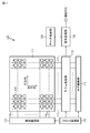
- FIG. 1 is a system configuration diagram illustrating a basic system configuration of a solid-state imaging device according to an embodiment of the present disclosure.
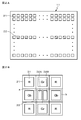
- FIG. 2A is a diagram for explaining pixel arrangement of the pixel array unit
- FIG. 2B is a diagram for explaining pixel sharing for sharing floating diffusion between pixels.
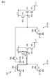
- FIG. 3 is a circuit diagram illustrating an example of a circuit configuration of an imaging pixel and a phase difference detection pixel that share a floating diffusion.
- FIG. 4 is an explanatory diagram of the cause of blooming.
- FIG. 5 is a timing chart for explaining a pixel operation when the technique of the present disclosure is not applied. 6A is an operation explanatory diagram at timing t 11 in FIG. 5, FIG. 6B is an operation explanatory diagram at timing t 12 in FIG.
- FIG. 5 is an operation explanatory diagram at timing t 13 in FIG. .
- FIG. 7 is a timing chart for explaining the pixel operation according to the embodiment when the technology of the present disclosure is applied.
- 8A is an operation explanatory diagram at timing t 21 in FIG. 7
- FIG. 8B is an operation explanatory diagram at timing t 22 in FIG. 7
- FIG. 8C is an operation explanatory diagram at timing t 23 in FIG.
- FIG. 9 is a cross-sectional view illustrating an example of a back-illuminated pixel structure.
- FIG. 10 is a block diagram illustrating an outline of a system configuration of an imaging apparatus that is an example of the electronic apparatus of the present disclosure.
- the transfer gate between the photoelectric conversion unit of the non-readout pixel and the floating diffusion in the reset period of the floating diffusion of the read pixel in the drive unit The height of the barrier under the gate of this part can be made lower than that during no charge transfer.
- the drive unit can be configured to apply a voltage lower than the voltage at the time of charge transfer to the gate electrode of the transfer gate unit during the reset period of the floating diffusion of the readout pixel.
- the non-read pixel sharing the floating diffusion is set to a distance from the subject using the phase difference of the subject image. It can be set as the structure which is a phase difference detection pixel for performing the phase difference detection to measure.
- the phase difference detection pixel includes the first photoelectric conversion unit and the second photoelectric conversion unit. It can be. At this time, it is preferable that the first photoelectric conversion unit shares the floating diffusion with the pixel adjacent to the first side of the phase difference detection pixel.
- the second photoelectric conversion unit preferably shares a floating diffusion with a pixel adjacent to the second side of the phase difference detection pixel.
- the unit pixel has a back-illuminated pixel structure.
- FIG. 1 is a system configuration diagram illustrating a basic system configuration of a solid-state imaging device according to an embodiment of the present disclosure.
- a CMOS image sensor which is a kind of XY address type solid-state image sensor will be described as an example of the solid-state image sensor according to the present embodiment.
- a CMOS image sensor is an image sensor created by applying or partially using a CMOS process.
- the solid-state imaging device 10 includes a pixel array unit 11 formed on a semiconductor substrate (semiconductor chip) (not shown) and a peripheral circuit unit integrated on the same semiconductor substrate as the pixel array unit 11. It is the composition which has.
- the peripheral circuit unit includes, for example, a vertical drive unit 12, a column processing unit 13, a horizontal drive unit 14, and a system control unit 15.
- the solid-state imaging device 10 further includes a signal processing unit 18 and a data storage unit 19.
- the signal processing unit 18 and the data storage unit 19 may be mounted on the same substrate as the solid-state imaging device 10 or may be arranged on a different substrate from the solid-state imaging device 10. Further, each processing of the signal processing unit 18 and the data storage unit 19 may be processing by an external signal processing unit provided on a substrate different from the solid-state imaging device 10, for example, a DSP (Digital Signal Processor) circuit or software. .
- DSP Digital Signal Processor
- the pixel array unit 11 performs photoelectric conversion to generate a photoelectric charge corresponding to the received light amount, and includes a photoelectric conversion unit that accumulates the unit pixel (hereinafter, may be simply referred to as “pixel”).
- 20 is two-dimensionally arranged in the row direction and the column direction, that is, in a matrix.
- the row direction refers to the pixel arrangement direction (that is, the horizontal direction) of the pixel row
- the column direction refers to the pixel arrangement direction (that is, the vertical direction) of the pixel column. Details of the specific circuit configuration and pixel structure of the unit pixel 20 will be described later.
- the pixel drive lines 16 (16 1 to 16 m ) are wired in the row direction for each pixel row with respect to the matrix pixel array, and the vertical signal lines 17 (17 1 ) are provided for each pixel column. ⁇ 17 n ) are wired along the column direction.
- the pixel drive line 16 transmits a drive signal, which will be described later, for driving when a signal is read from the pixel.
- the pixel drive line 16 is shown as one wiring, but is not limited to one.
- One end of the pixel drive line 16 is connected to an output end corresponding to each row of the vertical drive unit 12.
- the vertical drive unit 12 is configured by a shift register, an address decoder, and the like, and drives each pixel 20 of the pixel array unit 11 at the same time or in units of rows. That is, the vertical drive unit 12 constitutes a drive unit that drives each pixel 20 of the pixel array unit 11 together with the system control unit 15 that controls the vertical drive unit 12.
- the vertical drive unit 12 is not shown in the figure for its specific configuration, but generally has a configuration having two scanning systems, a reading scanning system and a sweeping scanning system.
- the readout scanning system sequentially scans the unit pixels 20 of the pixel array unit 11 in order of rows in order to read out signals from the unit pixels 20.
- a signal read from the unit pixel 20 is an analog signal.
- the sweep-out scanning system performs sweep-out scanning on the readout line on which readout scanning is performed by the readout scanning system prior to the readout scanning by the time corresponding to the shutter speed.
- a so-called electronic shutter operation is performed by sweeping (resetting) unnecessary charges by the sweep scanning system.
- the electronic shutter operation refers to an operation in which the photoelectric charge of the photoelectric conversion unit is discarded and exposure is newly started (photocharge accumulation is started).
- the signal read out by the readout operation by the readout scanning system corresponds to the amount of light received after the immediately preceding readout operation or electronic shutter operation.
- a period from the read timing by the immediately preceding read operation or the sweep timing by the electronic shutter operation to the read timing by the current read operation is the photo charge exposure period in the unit pixel 20.
- the signal output from each unit pixel 20 in the pixel row selectively scanned by the vertical drive unit 12 is input to the column processing unit 13 through each of the vertical signal lines 17 for each pixel column.
- the column processing unit 13 performs predetermined signal processing on a signal output from each pixel 20 of the selected row through the vertical signal line 17 for each pixel column of the pixel array unit 11, and outputs a pixel signal after the signal processing. Hold temporarily.
- the column processing unit 13 performs at least noise removal processing, for example, CDS (Correlated Double Sampling) processing or DDS (Double Data Sampling) processing as signal processing.
- CDS Correlated Double Sampling
- DDS Double Data Sampling
- pixel-specific fixed pattern noise such as reset noise and variation in threshold values of amplification transistors in the pixel 20 is removed by CDS processing.
- the column processing unit 13 may have, for example, an AD (analog-digital) conversion function to convert an analog pixel signal into a digital signal and output the digital signal.
- AD analog-digital
- the horizontal drive unit 14 includes a shift register, an address decoder, and the like, and sequentially selects unit circuits corresponding to the pixel columns of the column processing unit 13. By the selective scanning by the horizontal driving unit 14, pixel signals subjected to signal processing for each unit circuit in the column processing unit 13 are sequentially output.
- the system control unit 15 includes a timing generator that generates various timing signals, and the vertical driving unit 12, the column processing unit 13, and the horizontal driving unit 14 based on various timings generated by the timing generator. Drive control is performed.
- the signal processing unit 18 has at least an arithmetic processing function, and performs various signal processing such as arithmetic processing on the pixel signal output from the column processing unit 13.
- the data storage unit 19 temporarily stores data necessary for the signal processing in the signal processing unit 18.
- the technique of the present disclosure is characterized by the circuit configuration of the unit pixel 20 and the drive unit of the unit pixel 20, in particular, the drive timing of the vertical drive unit 12. Specific examples of the circuit configuration of the unit pixel 20 and the driving timing of the vertical driving unit 12 will be described later.
- the above system configuration is an example and is not limited to this.
- the column processing unit 13 is provided with an AD conversion function for performing AD conversion for each column of the pixel array unit 11 or for each of a plurality of columns, and a data storage unit 19 and a signal processing unit 18 are provided to the column processing unit 13.
- a system configuration may be provided in parallel.
- FIGS. 2A and 2B are diagrams for explaining pixel arrangement of the pixel array unit 11 of the solid-state imaging device 10 according to the present embodiment.
- 2A is a diagram for explaining pixel arrangement of the pixel array unit 11
- FIG. 2B is a diagram for explaining pixel sharing in which floating diffusion is shared between pixels.
- the unit pixel 20 includes a normal imaging pixel 21 for generating a captured image and a phase difference detection pixel 22 for detecting a phase difference.
- the imaging pixels 21 (open squares in the figure) are two-dimensionally arranged in a matrix in the pixel array unit 11.
- the imaging pixel 21 includes an R pixel that receives a red light by forming a red color filter layer, a G pixel that forms a green color filter layer and receives a green light, and a blue color filter layer that forms a blue light. It consists of B pixels that receive light, and these pixels are regularly arranged according to the Bayer array.
- each pixel of RGB is illustrated, this is an example and is not limited to the RGB pixel arrangement.
- a pixel array including pixels that receive white light or pixels that receive complementary color light such as yellow may be used.
- the phase difference detection pixels 22 are scattered in the imaging pixels 21 that are two-dimensionally arranged in a matrix. Specifically, the phase difference detection pixels 22 are regularly arranged in a specific pattern in the pixel array unit 11 instead of some imaging pixels 21. Note that the arrangement of the imaging pixels 21 and the phase difference detection pixels 22 is not limited to the arrangement shown in FIG. 2A, and may be arranged in another pattern.
- the imaging pixel 21 includes one photoelectric conversion unit 31.
- the imaging pixel 21 outputs a signal for generating a captured image by photoelectrically converting the received image light of the subject by the photoelectric conversion unit 31.
- the phase difference detection pixel 22 includes a first photoelectric conversion unit 32A and a second photoelectric conversion unit 32B.
- the first photoelectric conversion unit 32A and the second photoelectric conversion unit 32B are used for phase difference detection that measures the distance to the subject using the phase difference of the subject image. That is, the phase difference detection pixel 22 uses the phase difference detection type autofocus by performing photoelectric conversion on the received image light of the subject by the first photoelectric conversion unit 32A and the second photoelectric conversion unit 32B. A signal for detection is output.
- the first photoelectric conversion unit 32 ⁇ / b> A and the second photoelectric conversion unit 32 ⁇ / b> B capture a floating diffusion (floating diffusion region / impurity diffusion region), which will be described later, from the imaging pixel 21 adjacent to the phase difference detection pixel 22.
- the photoelectric conversion unit 31 is shared.
- the first photoelectric conversion unit 32A shares a floating diffusion with the photoelectric conversion unit 31 of the imaging pixel 21 adjacent to the first side (lower side of the drawing) of the phase difference detection pixel 22. (Combination surrounded by broken line a in the figure).
- the second photoelectric conversion unit 32B shares a floating diffusion with the photoelectric conversion unit 31 of the imaging pixel 21 adjacent to the second side (right side in the drawing) of the phase difference detection pixel 22 (a combination surrounded by a broken line b in the drawing). .
- the floating diffusion shared between the phase difference detection pixel 22 and the imaging pixel 21 adjacent to the first side of the phase difference detection pixel 22 is photoelectrically converted by the photoelectric conversion unit 31 or the first photoelectric conversion unit 32A. Convert charge to voltage.
- the floating diffusion shared between the phase difference detection pixel 22 and the imaging pixel 21 adjacent to the second side of the phase difference detection pixel 22 was photoelectrically converted by the photoelectric conversion unit 31 or the second photoelectric conversion unit 32B. Convert charge to voltage.
- the combination of the phase difference detection pixel 22 and the imaging pixel 21 adjacent to the phase difference detection pixel 22 is not limited to the combination shown in FIG. 2B.
- a combination of the phase difference detection pixel 22 and the imaging pixel 21 adjacent to the phase difference detection pixel 22 in the vertical direction may be used.
- Gr pixel means a G pixel in a pixel row including an R pixel
- Gb pixel means a G pixel in a pixel row including a B pixel.
- FIG. 3 is a circuit diagram showing an example of the circuit configuration of the imaging pixel 21 and the phase difference detection pixel 22 that share the floating diffusion.
- FIG. 3 illustrates a circuit configuration of one phase difference detection pixel 22 in FIG. 2B and two imaging pixels 21Gr and 21Gb adjacent to the phase difference detection pixel 22.
- each of the imaging pixels 21Gr and 21Gb includes a transfer transistor 41 that is a transfer gate unit, a floating diffusion (FD) 42, a reset transistor 43, an amplification transistor 44, and a selection transistor 45.
- the photoelectric conversion unit 31 is composed of, for example, a photodiode PD.
- the phase difference detection pixel 22 includes a transfer transistor (transfer gate unit) 41 and a floating diffusion 42 corresponding to each of the photoelectric conversion units 32A and 32B. , A reset transistor 43, an amplification transistor 44, and a selection transistor 45.
- the first photoelectric conversion unit 32A and the second photoelectric conversion unit 32B are composed of, for example, a photodiode PD.
- the first photoelectric conversion unit 32 ⁇ / b> A includes the photoelectric conversion unit 31 of the imaging pixel 21 ⁇ / b> Gr (see FIG. 2B) adjacent below the phase difference detection pixel 22, and the floating diffusion. 42, the amplification transistor 44, and the selection transistor 45 are shared.
- the second photoelectric conversion unit 32B includes the photoelectric conversion unit 31 of the imaging pixel 21Gb (see FIG. 2B) adjacent to the right side of the phase difference detection pixel 22, the floating diffusion 42, the amplification transistor 44, and the selection.
- the transistor 45 is shared.
- the transfer pulse TRG is applied to the gate electrode from the vertical drive unit 12 (see FIG. 1), so that the photoelectric conversion unit 31 / first photoelectric conversion unit 32A / second photoelectric conversion unit 32B perform photoelectric conversion.
- the converted charge is transferred to the floating diffusion 42.
- the floating diffusion 42 converts the charges transferred (read out) from the photoelectric conversion unit 31 / first photoelectric conversion unit 32A / second photoelectric conversion unit 32B into a voltage.
- the reset transistor 43 resets the floating diffusion 42 when a reset pulse RST is applied to the gate electrode from the vertical driving unit 12.
- the amplification transistor 44 outputs the pixel signal converted into the voltage by the floating diffusion 42 to the vertical signal line 17 through the selection transistor 45.
- the selection transistor 45 selectively connects the amplification transistor 44 to the vertical signal line 17 when a selection pulse SEL is applied from the vertical drive unit 12.
- the two photoelectric conversion units 32A and 32B share the floating diffusion 42 and the amplification transistor 44 of different adjacent pixels, respectively. Can be simultaneously exposed and read out.
- the path of the first photoelectric conversion unit 32A ⁇ the transfer transistor 41 ⁇ the reset transistor 43 ⁇ the power supply V DD shown by a broken line in FIG. Is an overflow path.
- the charge accumulation time (exposure time) of the pixel row including the phase difference detection pixel 22 is imaged. It may be set longer than the pixel row including the pixels 21Gr and 21Gb.
- the accumulation time is set to be long, the first photoelectric conversion unit 32A and the second photoelectric conversion unit 32B of the phase difference detection pixel 22 overflow when a large amount of light is input, which causes blooming.
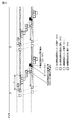
- FIG. 4 is an explanatory diagram of the cause of blooming.
- XVS represents a vertical synchronization signal
- T represents a time until the charge overflows in the photoelectric conversion units 32A and 32B of the phase difference detection pixel 22.
- the open dashed square indicates the shutter timing phase difference detection pixel 22
- the shaded dashed square indicates the readout timing phase difference detection pixel 22
- the open solid square indicates the shutter timing imaging pixel.
- the shaded solid line squares indicate the image pickup pixels 21 at the read timing.
- the charge accumulation time of the pixel row including the phase difference detection pixel 22 is set long has been described as an example, but the present invention is not limited to the pixel row including the phase difference detection pixel 22, It can be considered that blooming also occurs in the image row including the imaging pixel 21 depending on the setting of the accumulation time.
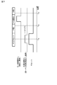
- FIG. 5 is a timing chart for explaining the pixel operation when the technique of the present disclosure is not applied.
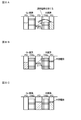
- FIG. 6 shows the potential of the photoelectric conversion unit (PD), the transfer gate unit (transfer transistor) at each timing of FIG. 41) is an operation explanatory view showing the barrier under the gate of 41) and the potential of the floating diffusion (FD).
- FIG. 5 shows a transfer pulse TRG for a pixel row including a readout pixel for reading out accumulated charges, a transfer pulse TRG for a pixel row including a non-readout pixel sharing the same floating diffusion 42 as the readout pixel, and a reset pulse.
- the timing relationship of RST is shown.
- the readout pixel is a Gr pixel and the non-readout pixel is a B pixel.
- FIG. 6A shows an operation explanatory diagram at timing t 11 in FIG. 5
- FIG. 6B shows an operation explanatory diagram at timing t 12 in FIG. 5
- FIG. 6C shows an operation explanation at timing t 13 in FIG.
- the timing t 11 is a reset timing of the floating diffusion FD.
- the timing t 12 is a read timing of the signal after resetting of the floating diffusion FD (so-called, P-phase).
- the timing t 13 is a read timing of the signal after reading charges from the photoelectric conversion unit PD to the floating diffusion FD (so-called, D-phase).
- the B pixel which is a non-read pixel reaches a saturation level.
- unnecessary charges of the B pixel flow over the barrier below the gate of the transfer transistor 41 and flow into the floating diffusion FD shared with the Gr pixel.
- this overflowed unnecessary charge is added to the original signal charge of the Gr pixel during the D phase, and as a result, blooming due to overflow of unnecessary charge from the adjacent pixel occurs. Visible as white streaks.
- a part of the charge of the non-readout pixel is discarded in advance in the floating diffusion FD shared with the read pixel during the reset period of the floating diffusion FD of the read pixel, so that photoelectric conversion of the non-readout pixel is performed when a large amount of light is input.
- the part PD can be prevented from overflowing. As a result, it is possible to prevent the unnecessary charge of the non-read pixel from flowing into the floating diffusion FD of the adjacent pixel sharing the floating diffusion FD, thereby suppressing the occurrence of blooming due to the overflow of the unnecessary charge from the adjacent pixel. Can do.
- the height of the barrier below the gate of the transfer transistor (transfer gate unit) 41 is made lower than that at the time of no charge transfer, thereby reducing the charge of the non-readout pixel. It is characterized in that a part is thrown away into the floating diffusion FD shared with the readout pixels. More specifically, a voltage lower than the voltage at the time of charge transfer, for example, a voltage of about half (so-called half bias) is applied to the gate electrode of the transfer transistor 41 as the transfer pulse TRG, whereby the gate of the transfer transistor 41 is transferred. The height of the lower barrier is made lower than when no charge is transferred.
- FIG. 7 is a timing chart for explaining the pixel operation according to the embodiment when the technology of the present disclosure is applied.
- FIG. 8 is a diagram illustrating the potential of the photoelectric conversion unit (PD) and the transfer gate at each timing in FIG.
- FIG. 6 is an operation explanatory diagram showing a barrier under a gate of a portion (transfer transistor 41) and a potential of a floating diffusion (FD).
- FIG. 7 shows a transfer pulse TRG for a pixel row including a readout pixel for reading out accumulated charges, a transfer pulse TRG for a pixel row including a non-readout pixel sharing the same floating diffusion 42 as the readout pixel, and a reset pulse.
- the timing relationship of RST is shown.
- the readout pixel is a Gr pixel
- the non-readout pixel is a B pixel.
- the transfer pulse TRG and the reset pulse RST pass through the pixel driving line 16 (16 1 to 16 m ) from the vertical driving unit 12 shown in FIG. 1 to the unit pixel 20 (the imaging pixel 21 and the phase difference detection pixel 22). Output in units.
- FIG. 8A shows an operation explanatory diagram at timing t 21 in FIG. 7
- FIG. 8B shows an operation explanatory diagram at timing t 22 in FIG. 7
- FIG. 8C shows an operation explanation at timing t 23 in FIG.
- the timing t 21 is a reset timing of the floating diffusion FD.
- the timing t 22 is a read timing of the signal after resetting of the floating diffusion FD (P phase).
- the timing t 23 is a read timing signal (D-phase) after reading charges from the photoelectric conversion unit PD to the floating diffusion FD.
- the transfer pulse TRG of the B pixel that is the non-readout pixel is set to a half bias so that, as shown in FIG. The height of the barrier is lower than when no charge is transferred. As a result, the excess charge of the B pixel is discarded to the floating diffusion FD in the reset state.
- the above-described technique for preventing blooming according to the present embodiment can be applied to the front-side illumination type pixel structure of the unit pixel 20, but the effect is more remarkable when applied to the back-side illumination type pixel structure.
- the “backside-illuminated pixel structure” refers to the second surface opposite to the first surface, that is, the substrate rear surface side, when the first surface on the side where the wiring layer of the semiconductor substrate is formed is the substrate surface.
- the “front-illuminated pixel structure” refers to a pixel structure that takes in incident light (irradiates light) from the substrate surface side.
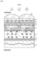
- FIG. 9 is a cross-sectional view illustrating an example of a back-illuminated pixel structure. Here, a cross-sectional structure for two pixels is shown.
- a photoelectric conversion part (photodiode) 31 and pixel transistors (transistors 41, 43 to 45 in FIG. 3) are formed on a semiconductor substrate 51.
- a color filter 53 is formed on the back side of the semiconductor substrate 51 via an insulating film 52.
- a planarizing film 54 is stacked on the color filter 53, and a microlens (on-chip lens) 55 is sequentially stacked on the planarizing film 54.
- a wiring layer 57 is formed, in which the gate electrodes and metal wirings of the pixel transistors (transistors 41, 43 to 45 in FIG. 3) are multilayered.
- a support substrate 59 is attached to the surface of the interlayer insulating film 56 opposite to the semiconductor substrate 51 with an adhesive 58.
- the photoelectric conversion unit 31 having the same area is compared with the front-illuminated pixel structure.
- the degree of freedom in wiring layout is increased, and the pixel is finer than the surface irradiation type pixel structure. Can be achieved.
- an overflow path (blooming pulse) can be formed on the bulk side, whereas in the case of a back-illuminated pixel structure, as apparent from the pixel structure described above, the photoelectric conversion unit 31 This is an overflow path to the floating diffusion FD (42 in FIG. 3).
- the blooming countermeasure method according to the present embodiment is particularly useful when applied to a back-illuminated pixel structure.
- the present invention is not limited to the application to the back-illuminated pixel structure, and may be applied to the front-illuminated pixel structure.
- the present invention can be applied to a solid-state imaging device using a technique for expanding the dynamic range.
- the following two methods can be exemplified as techniques for expanding the dynamic range.
- Time division method A method in which time-division is taken with different sensitivities depending on the accumulation time, and a plurality of images taken in time division are combined to expand the dynamic range. In this time division method, the dynamic range can be expanded by increasing the number of time division divisions.
- Space division method A method in which a plurality of pixels with different color filter sensitivities are provided, and a plurality of images photographed by the plurality of pixels having different sensitivities are combined to expand the dynamic range.
- the dynamic range can be expanded by increasing the number of space divisions.
- the so-called column processing unit 13, the signal processing unit 18, the data storage unit 19, and the like are mounted on the same semiconductor substrate together with the pixel array unit 11. , It can be a flat structure.
- components such as the column processing unit 13, the signal processing unit 18, and the data storage unit 19 are distributed and mounted on one or more other semiconductor substrates different from the semiconductor substrate on which the pixel array unit 11 is mounted.
- a so-called stacked structure in which these semiconductor substrates are stacked can be obtained.
- the solid-state imaging device is an imaging device such as a digital still camera or a video camera, a portable terminal device having an imaging function such as a mobile phone, a copying machine using a solid-state imaging device for an image reading unit, or the like. It can be used as an imaging unit (image capturing unit) in all electronic devices. In addition, it is used in the field of traffic such as in-vehicle sensors that capture the front, rear, surroundings, and interiors of automobiles, surveillance cameras that monitor traveling vehicles and roads, and ranging sensors that measure distances between vehicles. It can also be used for devices used in the medical and healthcare fields, such as devices, endoscopes, and devices that perform angiography by receiving infrared light.
- the solid-state imaging device may be formed as a single chip, or may be in a modular form having an imaging function in which an imaging unit and a signal processing unit or an optical system are packaged together. Good.
- a camera module is used as an imaging device.
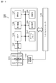
- FIG. 10 is a block diagram illustrating an outline of a system configuration of an imaging apparatus that is an example of the electronic apparatus of the present disclosure.
- the imaging device 100 of the present disclosure includes an imaging optical system 101, an imaging unit 102, a DSP circuit 103 that is a camera signal processing unit, a frame memory 104, a display device 105, a recording device 106, an operation system 107, And a power supply system 108 and the like.
- a DSP circuit 103, a frame memory 104, a display device 105, a recording device 106, an operation system 107, and a power supply system 108 are connected to each other via a bus line 109 so that they can communicate with each other.
- the imaging apparatus 100 further includes an optical system driving unit 110 and a system controller 120.
- the imaging optical system 101 includes a zoom lens a, a diaphragm b, a focus lens c, and the like, takes in incident light (image light) from a subject and forms an image on the imaging surface of the imaging unit 102.
- the zoom lens a changes the focal length by moving in the optical axis O direction under the driving of the optical system driving unit 110, thereby adjusting the magnification of the subject included in the captured image.
- the diaphragm b adjusts the amount of image light of the subject incident on the imaging surface of the imaging unit 102 by changing the degree of opening under the driving of the optical system driving unit 110.
- the focus lens c adjusts the focus by moving in the direction of the optical axis O under the driving of the optical system driving unit 110.
- the imaging unit 102 converts the amount of image light (incident light) of the subject imaged on the imaging surface by the imaging optical system 101 into an electrical signal for each pixel and outputs the electrical signal as a pixel signal.
- the imaging unit 102 the solid-state imaging device according to the above-described embodiment that includes a phase difference detection pixel in the pixel array unit and shares the floating diffusion FD between adjacent pixels can be used.
- the display device 105 includes a panel type display device such as a liquid crystal display device or an organic EL (electroluminescence) display device, and displays a moving image or a still image captured by the imaging unit 102.
- the recording device 106 records the moving image or still image captured by the imaging unit 102 on a recording medium such as a portable semiconductor memory, an optical disk, or an HDD (Hard Disk Disk Drive).
- the operation system 107 issues operation commands for various functions of the imaging apparatus 100 under the operation of the user.
- the power supply system 108 appropriately supplies various power supplies serving as operation power for the DSP circuit 103, the frame memory 104, the display device 105, the recording device 106, and the operation system 107 to these supply targets.
- the optical system driving unit 110 drives the zoom lens a, the diaphragm b, the focus lens c, and the like of the imaging optical system 101 under the control of the system controller 120.
- the system controller 120 performs various controls such as auto focus control of the imaging optical system 101 and control of each of the above components.
- the DSP circuit 103 calculates a defocus direction and a defocus amount based on the phase difference detection signal output from the phase difference detection pixel in the solid-state imaging device according to the above-described embodiment. Processing is performed.
- the system controller 120 performs focus control to bring the focus lens c into the focused state by moving the focus lens c in the direction of the optical axis O via the optical system driving unit 110.
- the solid-state imaging device As described above, by using the solid-state imaging device according to the above-described embodiment as the imaging unit 102, the following operations and effects can be obtained. That is, according to the solid-state imaging device, it is possible to prevent the charge of the non-read pixel from flowing into the floating diffusion of the adjacent pixel sharing the floating diffusion, so that blooming due to overflow of unnecessary charge from the adjacent pixel can be prevented. Occurrence can be suppressed. Therefore, by using the solid-state imaging device according to the above-described embodiment as the imaging unit 102, a high-quality captured image without blooming can be obtained.
- a pixel array unit in which unit pixels including a photoelectric conversion unit are two-dimensionally arranged in a matrix and share a floating diffusion among a plurality of unit pixels;
- a solid-state imaging device A solid-state imaging device.
- the drive unit sets the height of the barrier below the gate of the transfer gate unit between the photoelectric conversion unit and the floating diffusion of the non-read pixel during the reset period of the floating diffusion of the read pixel, compared to when the charge is not transferred.
- the solid-state imaging device lower, The solid-state imaging device according to [1] above.
- the drive unit applies a voltage lower than the voltage at the time of charge transfer to the gate electrode of the transfer gate unit during the reset period of the floating diffusion of the readout pixel.
- the solid-state imaging device according to the above [2].
- the non-read pixel sharing the floating diffusion is a phase difference detection pixel for performing phase difference detection that measures the distance to the subject using the phase difference of the subject image.
- the solid-state imaging device according to any one of [1] to [3] above.
- the phase difference detection pixel includes a first photoelectric conversion unit and a second photoelectric conversion unit, The first photoelectric conversion unit shares a floating diffusion with a pixel adjacent to the first side of the phase difference detection pixel, The second photoelectric conversion unit shares a floating diffusion with a pixel adjacent to the second side of the phase difference detection pixel.
- the solid-state imaging device according to [4] above.
- the unit pixel has a back-illuminated pixel structure.
- the solid-state imaging device according to any one of [1] to [5] above.
- the method for driving a solid-state imaging device according to the above [7]. [9] A voltage lower than the voltage at the time of charge transfer is applied to the gate electrode of the transfer gate portion during the reset period of the floating diffusion of the readout pixel. The method for driving a solid-state imaging device according to the above [8]. [10] The non-read pixel sharing the floating diffusion is a phase difference detection pixel for performing phase difference detection that measures the distance to the subject using the phase difference of the subject image. The method for driving a solid-state imaging device according to any one of [7] to [9] above.
- the phase difference detection pixel includes a first photoelectric conversion unit and a second photoelectric conversion unit, The first photoelectric conversion unit shares a floating diffusion with a pixel adjacent to the first side of the phase difference detection pixel, The second photoelectric conversion unit shares a floating diffusion with a pixel adjacent to the second side of the phase difference detection pixel.
- the unit pixel has a back-illuminated pixel structure. The method for driving a solid-state imaging device according to any one of [7] to [11] above.
- a pixel array unit in which unit pixels including a photoelectric conversion unit are two-dimensionally arranged in a matrix and share a floating diffusion among a plurality of unit pixels;
- a drive unit for driving to discard a part of the charge of the non-read pixel that shares the floating diffusion with the read pixel in the floating diffusion during the reset period of the floating diffusion of the read pixel for reading the charge;
- a solid-state imaging device comprising: Electronics.
- SYMBOLS 10 Solid-state image sensor, 11 ... Pixel array part, 12 ... Vertical drive part, 13 ... Column processing part, 14 ... Vertical drive part, 15 ... System control part, 16 ( 16 1 to 16 m )... Pixel drive line, 17 (17 1 to 17 n )... Vertical signal line, 18... Signal processing unit, 19. , 21 ... imaging pixels, 22 ... phase difference detection pixels, 31, 32A, 32B ... photoelectric conversion part, 41 ... transfer transistor (transfer gate part), 42 ... floating diffusion (FD) 43 ... Reset transistor, 44 ... Amplification transistor, 45 ... Selection transistor
Landscapes
- Engineering & Computer Science (AREA)
- Multimedia (AREA)
- Signal Processing (AREA)
- Physics & Mathematics (AREA)
- General Physics & Mathematics (AREA)
- Optics & Photonics (AREA)
- Solid State Image Pick-Up Elements (AREA)
- Transforming Light Signals Into Electric Signals (AREA)
- Focusing (AREA)
- Automatic Focus Adjustment (AREA)
Abstract
本開示の固体撮像素子は、光電変換部を含む単位画素が行列状に2次元配置され、複数の単位画素間でフローティングディフュージョンを共有する画素アレイ部と、電荷を読み出す読出し画素のフローティングディフュージョンのリセット期間に、読出し画素とフローティングディフュージョンを共有する非読出し画素の電荷の一部をフローティングディフュージョンに捨てる駆動を行う駆動部と、を備える。
Description
本開示は、固体撮像素子、固体撮像素子の駆動方法、及び、電子機器に関する。
撮像装置において、自動的に焦点(ピント)が合った状態(即ち、合焦状態)にするオートフォーカス(Auto Focus:AF)の方式の一つとして、位相差検出方式が知られている。位相差検出方式のオートフォーカスは、2つのセンサーを用いて被写体像の位相差を利用し、被写体と撮像レンズとの間の距離を測定してピントを合わせる方式である。この位相差検出方式のオートフォーカスを実現するために、撮像画像を生成するための通常の撮像画素が行列状に2次元配置されて成る画素アレイ部内に、一部の撮像画素に代えて、位相差検出を行うための位相差検出画素を設けた構成の固体撮像素子がある。
この位相差検出方式のオートフォーカスを実現するための固体撮像素子において、位相差検出画素は複数の光電変換部を有している。また、オートフォーカスの速度と精度の向上を図るために、位相差検出画素の複数の光電変換部の各々が、位相差検出画素に隣接する撮像画素との間で、フローティングディフュージョンを共有するようにしている(例えば、特許文献1参照)。
ところで、画素アレイ部内に位相差検出画素を設けて成る固体撮像素子において、例えば暗い環境下でも精度良くオートフォーカスを行うために、位相差検出画素を含む画素行の電荷の蓄積時間を、通常の撮像画素を含む画素行に比べて長く設定することがある。このように、位相差検出画素を含む画素行の電荷の蓄積時間を長く設定すると、大光量の入力時に、位相差検出画素の光電変換部がオーバーフローする場合がある。そして、位相差検出画素の光電変換部がオーバーフローすると、位相差検出画素から溢れた電荷が、フローティングディフュージョンを共有する隣接画素の当該フローティングディフュージョンに流れ込み、ブルーミングの発生原因となる。
本開示は、光電変換部から溢れた電荷が、フローティングディフュージョンを共有する隣接画素の当該フローティングディフュージョンに流れ込むことを阻止できる固体撮像素子、固体撮像素子の駆動方法、及び、当該固体撮像素子を有する電子機器を提供することを目的とする。
上記の目的を達成するための本開示の固体撮像素子は、
光電変換部を含む単位画素が行列状に2次元配置され、複数の単位画素間でフローティングディフュージョンを共有する画素アレイ部と、
電荷を読み出す読出し画素のフローティングディフュージョンのリセット期間に、読出し画素とフローティングディフュージョンを共有する非読出し画素の電荷の一部をフローティングディフュージョンに捨てる駆動を行う駆動部と、
を備える。また、上記の目的を達成するための本開示の電子機器は、上記の構成の固体撮像素子を有する。
光電変換部を含む単位画素が行列状に2次元配置され、複数の単位画素間でフローティングディフュージョンを共有する画素アレイ部と、
電荷を読み出す読出し画素のフローティングディフュージョンのリセット期間に、読出し画素とフローティングディフュージョンを共有する非読出し画素の電荷の一部をフローティングディフュージョンに捨てる駆動を行う駆動部と、
を備える。また、上記の目的を達成するための本開示の電子機器は、上記の構成の固体撮像素子を有する。
また、上記の目的を達成するための本開示の固体撮像素子の駆動方法は、
光電変換部を含む単位画素が行列状に2次元配置され、複数の単位画素間でフローティングディフュージョンを共有する固体撮像素子の駆動に当たって、
電荷を読み出す読出し画素のフローティングディフュージョンのリセット期間に、読出し画素とフローティングディフュージョンを共有する非読出し画素の電荷の一部をフローティングディフュージョンに捨てる。
光電変換部を含む単位画素が行列状に2次元配置され、複数の単位画素間でフローティングディフュージョンを共有する固体撮像素子の駆動に当たって、
電荷を読み出す読出し画素のフローティングディフュージョンのリセット期間に、読出し画素とフローティングディフュージョンを共有する非読出し画素の電荷の一部をフローティングディフュージョンに捨てる。
読出し画素のフローティングディフュージョンのリセット期間に、非読出し画素の電荷の一部をフローティングディフュージョンに捨てる。この捨てる動作はリセット期間での動作であるため、捨てられた電荷がフローティングディフュージョンに残存しない。従って、非読出し画素の電荷の一部を、読出し画素のフローティングディフュージョンのリセット期間にあらかじめ、共有するフローティングディフュージョンに捨てることにより、大光量の入力時に、非読出し画素の光電変換部がオーバーフローしないようにすることができる。これにより、フローティングディフュージョンを共有する隣接画素の当該フローティングディフュージョンに、非読出し画素の電荷が流れ込むことを阻止できる。
本開示によれば、フローティングディフュージョンを共有する隣接画素の当該フローティングディフュージョンに、非読出し画素の電荷が流れ込むことを阻止できるため、オーバーフローに起因するブルーミングの発生を抑えることができる。
尚、ここに記載された効果に必ずしも限定されるものではなく、本明細書中に記載されたいずれかの効果であってもよい。また、本明細書に記載された効果はあくまで例示であって、これに限定されるものではなく、また付加的な効果があってもよい。
以下、本開示の技術を実施するための形態(以下、「実施形態」と記述する)について図面を用いて詳細に説明する。本開示の技術は実施形態に限定されるものではない。以下の説明において、同一要素又は同一機能を有する要素には同一符号を用いることとし、重複する説明は省略する。尚、説明は以下の順序で行う。
1.本開示の固体撮像素子、その駆動方法、及び、電子機器、全般に関する説明
2.基本的なシステム構成
3.画素アレイ部の画素配置
4.単位画素の回路構成
5.ブルーミングの発生について
6.ブルーミング対策について
6-1.実施例(ブルーミング対策の具体例)
7.裏面照射型の画素構造
8.変形例
9.電子機器
9-1.撮像装置
10.本開示がとることができる構成
1.本開示の固体撮像素子、その駆動方法、及び、電子機器、全般に関する説明
2.基本的なシステム構成
3.画素アレイ部の画素配置
4.単位画素の回路構成
5.ブルーミングの発生について
6.ブルーミング対策について
6-1.実施例(ブルーミング対策の具体例)
7.裏面照射型の画素構造
8.変形例
9.電子機器
9-1.撮像装置
10.本開示がとることができる構成
<本開示の固体撮像素子、その駆動方法、及び、電子機器、全般に関する説明>
本開示の固体撮像素子、その駆動方法、及び、電子機器にあっては、駆動部について、読出し画素のフローティングディフュージョンのリセット期間に、非読出し画素の光電変換部とフローティングディフュージョンとの間の転送ゲート部のゲート下の障壁の高さを、電荷非転送時よりも下げる構成とすることができる。また、駆動部について、読出し画素のフローティングディフュージョンのリセット期間に、転送ゲート部のゲート電極に、電荷転送時の電圧よりも低い電圧を印加する構成とすることができる。
本開示の固体撮像素子、その駆動方法、及び、電子機器にあっては、駆動部について、読出し画素のフローティングディフュージョンのリセット期間に、非読出し画素の光電変換部とフローティングディフュージョンとの間の転送ゲート部のゲート下の障壁の高さを、電荷非転送時よりも下げる構成とすることができる。また、駆動部について、読出し画素のフローティングディフュージョンのリセット期間に、転送ゲート部のゲート電極に、電荷転送時の電圧よりも低い電圧を印加する構成とすることができる。
上述した好ましい構成を含む本開示の固体撮像素子、その駆動方法、及び、電子機器にあっては、フローティングディフュージョンを共有する非読出し画素を、被写体像の位相差を利用して被写体との距離を測定する位相差検出を行うための位相差検出画素である構成とすることができる。
また、上述した好ましい構成を含む本開示の固体撮像素子、その駆動方法、及び、電子機器にあっては、位相差検出画素について、第1の光電変換部及び第2の光電変換部を有する構成とすることができる。このとき、第1の光電変換部について、位相差検出画素の第1側に隣接する画素とフローティングディフュージョンを共有することが好ましい。また、第2の光電変換部について、位相差検出画素の第2側に隣接する画素とフローティングディフュージョンを共有することが好ましい。
また、上述した好ましい構成を含む本開示の固体撮像素子、その駆動方法、及び、電子機器にあっては、単位画素について、裏面照射型の画素構造を有する構成とすることが好ましい。
[基本的なシステム構成]
図1は、本開示の一実施形態に係る固体撮像素子の基本的なシステム構成を示すシステム構成図である。ここでは、本実施形態に係る固体撮像素子として、X-Yアドレス方式の固体撮像素子の一種であるCMOSイメージセンサを例に挙げて説明する。CMOSイメージセンサとは、CMOSプロセスを応用して、または、部分的に使用して作成されたイメージセンサである。
図1は、本開示の一実施形態に係る固体撮像素子の基本的なシステム構成を示すシステム構成図である。ここでは、本実施形態に係る固体撮像素子として、X-Yアドレス方式の固体撮像素子の一種であるCMOSイメージセンサを例に挙げて説明する。CMOSイメージセンサとは、CMOSプロセスを応用して、または、部分的に使用して作成されたイメージセンサである。
本実施形態に係る固体撮像素子10は、図示せぬ半導体基板(半導体チップ)上に形成された画素アレイ部11と、当該画素アレイ部11と同じ半導体基板上に集積された周辺回路部とを有する構成となっている。周辺回路部は、例えば、垂直駆動部12、カラム処理部13、水平駆動部14、及び、システム制御部15から構成されている。
固体撮像素子10は更に、信号処理部18及びデータ格納部19を備えている。信号処理部18及びデータ格納部19については、固体撮像素子10と同じ基板上に搭載しても構わないし、固体撮像素子10とは別の基板上に配置するようにしても構わない。また、信号処理部18及びデータ格納部19の各処理については、固体撮像素子10とは別の基板に設けられる外部信号処理部、例えば、DSP(Digital Signal Processor)回路やソフトウェアによる処理でも構わない。
画素アレイ部11は、光電変換を行うことで、受光した光量に応じた光電荷を生成し、かつ、蓄積する光電変換部を含む単位画素(以下、単に「画素」と記述する場合がある)20が行方向及び列方向に、即ち、行列状に2次元配置された構成となっている。ここで、行方向とは画素行の画素の配列方向(即ち、水平方向)を言い、列方向とは画素列の画素の配列方向(即ち、垂直方向)を言う。単位画素20の具体的な回路構成や画素構造の詳細については後述する。
画素アレイ部11において、行列状の画素配列に対して、画素行毎に画素駆動線16(161~16m)が行方向に沿って配線され、画素列毎に垂直信号線17(171~17n)が列方向に沿って配線されている。画素駆動線16は、画素から信号を読み出す際の駆動を行うための、後述する駆動信号を伝送する。図1では、画素駆動線16について1本の配線として示しているが、1本に限られるものではない。画素駆動線16の一端は、垂直駆動部12の各行に対応した出力端に接続されている。
垂直駆動部12は、シフトレジスタやアドレスデコーダなどによって構成され、画素アレイ部11の各画素20を全画素同時あるいは行単位等で駆動する。すなわち、垂直駆動部12は、当該垂直駆動部12を制御するシステム制御部15と共に、画素アレイ部11の各画素20を駆動する駆動部を構成している。この垂直駆動部12はその具体的な構成については図示を省略するが、一般的に、読出し走査系と掃出し走査系の2つの走査系を有する構成となっている。
読出し走査系は、単位画素20から信号を読み出すために、画素アレイ部11の単位画素20を行単位で順に選択走査する。単位画素20から読み出される信号はアナログ信号である。掃出し走査系は、読出し走査系によって読出し走査が行われる読出し行に対し、その読出し走査よりもシャッタスピードの時間分だけ先行して掃出し走査を行う。
この掃出し走査系による掃出し走査により、読出し行の単位画素20の光電変換部から不要な電荷が掃き出されることによって当該光電変換部がリセットされる。そして、この掃出し走査系による不要電荷の掃き出す(リセットする)ことにより、所謂電子シャッタ動作が行われる。ここで、電子シャッタ動作とは、光電変換部の光電荷を捨てて、新たに露光を開始する(光電荷の蓄積を開始する)動作のことを言う。
読出し走査系による読出し動作によって読み出される信号は、その直前の読出し動作または電子シャッタ動作以降に受光した光量に対応するものである。そして、直前の読出し動作による読出しタイミングまたは電子シャッタ動作による掃出しタイミングから、今回の読出し動作による読出しタイミングまでの期間が、単位画素20における光電荷の露光期間となる。
垂直駆動部12によって選択走査された画素行の各単位画素20から出力される信号は、画素列毎に垂直信号線17の各々を通してカラム処理部13に入力される。カラム処理部13は、画素アレイ部11の画素列毎に、選択行の各画素20から垂直信号線17を通して出力される信号に対して所定の信号処理を行うとともに、信号処理後の画素信号を一時的に保持する。
具体的には、カラム処理部13は、信号処理として少なくとも、ノイズ除去処理、例えばCDS(Correlated Double Sampling;相関二重サンプリング)処理や、DDS(Double Data Sampling)処理を行う。例えば、CDS処理により、リセットノイズや画素20内の増幅トランジスタの閾値ばらつき等の画素固有の固定パターンノイズが除去される。カラム処理部13にノイズ除去処理以外に、例えば、AD(アナログ-デジタル)変換機能を持たせ、アナログの画素信号をデジタル信号に変換して出力することも可能である。
水平駆動部14は、シフトレジスタやアドレスデコーダなどによって構成され、カラム処理部13の画素列に対応する単位回路を順番に選択する。この水平駆動部14による選択走査により、カラム処理部13において単位回路ごとに信号処理された画素信号が順番に出力される。
システム制御部15は、各種のタイミング信号を生成するタイミングジェネレータなどによって構成され、当該タイミングジェネレータで生成された各種のタイミングを基に、垂直駆動部12、カラム処理部13、及び、水平駆動部14などの駆動制御を行う。
信号処理部18は、少なくとも演算処理機能を有し、カラム処理部13から出力される画素信号に対して演算処理等の種々の信号処理を行う。データ格納部19は、信号処理部18での信号処理に当たって、その処理に必要なデータを一時的に格納する。
上記の構成の固体撮像素子10において、本開示の技術は、単位画素20の回路構成及び単位画素20の駆動部、特に、垂直駆動部12の駆動タイミングを特徴としている。単位画素20の回路構成及び垂直駆動部12の駆動タイミングの具体的な実施例については後述する。
尚、上記のシステム構成は、一例であって、これに限られるものではない。例えば、データ格納部19をカラム処理部13の後段に配置し、カラム処理部13から出力される画素信号を、データ格納部19を経由して信号処理部18に供給するシステム構成であってもよい。あるいは又、画素アレイ部11の列ごとあるいは複数の列ごとにAD変換するAD変換機能をカラム処理部13に持たせるとともに、当該カラム処理部13に対してデータ格納部19及び信号処理部18を並列的に設けるシステム構成であってもよい。
[画素アレイ部の画素配置]
次に、本実施形態に係る固体撮像素子10の画素アレイ部11の画素配置について、図2A及び図2Bを用いてより具体的に説明する。図2Aは、画素アレイ部11の画素配置について説明する図であり、図2Bは、画素間でフローティングディフュージョンを共有する画素共有について説明する図である。
次に、本実施形態に係る固体撮像素子10の画素アレイ部11の画素配置について、図2A及び図2Bを用いてより具体的に説明する。図2Aは、画素アレイ部11の画素配置について説明する図であり、図2Bは、画素間でフローティングディフュージョンを共有する画素共有について説明する図である。
単位画素20は、撮像画像を生成するための通常の撮像画素21と、位相差検出を行うための位相差検出画素22とから成る。図2Aに示すように、撮像画素21(図中、白抜きの正方形)は、画素アレイ部11に行列状に2次元配置されている。撮像画素21は、赤色カラーフィルタ層が形成されて赤色光を受光するR画素、緑色カラーフィルタ層が形成されて緑色光を受光するG画素、及び、青色カラーフィルタ層が形成されて青色光を受光するB画素から成り、これらの画素がベイヤー配列に従い規則的に配置されている。
ここでは、RGBの各画素の配列を例示したが、これは一例であってRGBの画素配列に限られるものではない。例えば、白色光を受光する画素や、黄色などの補色光を受光する画素を含む画素配列であってもよい。
図2Aに示すように、位相差検出画素22(図中、網掛けの正方形)は、行列状に2次元配置された撮像画素21の中に散在している。具体的には、位相差検出画素22は、画素アレイ部11において、一部の撮像画素21に代えて、特定のパターンで規則的に配置されている。尚、撮像画素21及び位相差検出画素22の配置は、図2Aに示す配置に限られるものではなく、他のパターンで配置されるようにしてもよい。
図2Bに示すように、撮像画素21は、1つの光電変換部31を備えている。撮像画素21は、受光した被写体の像光を光電変換部31で光電変換することにより、撮像画像を生成するための信号を出力する。位相差検出画素22は、第1の光電変換部32A及び第2の光電変換部32Bを備えている。第1の光電変換部32A及び第2の光電変換部32Bは、被写体像の位相差を利用して被写体との距離を測定する位相差検出に用いられる。すなわち、位相差検出画素22は、受光した被写体の像光を第1の光電変換部32A及び第2の光電変換部32Bで光電変換することにより、位相差検出方式のオートフォーカスに用いる、位相差検出を行うための信号を出力する。
位相差検出画素22において、第1の光電変換部32A及び第2の光電変換部32Bは、後述するフローティングディフュージョン(浮遊拡散領域/不純物拡散領域)を、位相差検出画素22に隣接する撮像画素21の光電変換部31と共用する。例えば、図2Bに示すように、第1の光電変換部32Aは、位相差検出画素22の第1側(図の下側)に隣接する撮像画素21の光電変換部31とフローティングディフュージョンを共有する(図中、破線aで囲む組み合わせ)。第2の光電変換部32Bは、位相差検出画素22の第2側(図の右側)に隣接する撮像画素21の光電変換部31とフローティングディフュージョンを共有する(図中、破線bで囲む組み合わせ)。
位相差検出画素22と当該位相差検出画素22の第1側に隣接する撮像画素21との間で共有されるフローティングディフュージョンは、光電変換部31又は第1の光電変換部32Aで光電変換された電荷を電圧に変換する。位相差検出画素22と当該位相差検出画素22の第2側に隣接する撮像画素21との間で共有されるフローティングディフュージョンは、光電変換部31又は第2の光電変換部32Bで光電変換された電荷を電圧に変換する。
尚、位相差検出画素22と当該位相差検出画素22に隣接する撮像画素21との組み合わせについては、図2Bに示す組み合わせに限られるものではない。例えば、位相差検出画素22と、当該位相差検出画素22に対して上下に隣接する撮像画素21との組み合わせ等であってもよい。図2Bにおいて、Gr画素は、R画素を含む画素行のG画素を意味し、Gb画素は、B画素を含む画素行のG画素を意味している。
[単位画素の回路構成]
次に、フローティングディフュージョンを共有する撮像画素21及び位相差検出画素22の回路構成について図3を用いて説明する。図3は、フローティングディフュージョンを共有する撮像画素21及び位相差検出画素22の回路構成の一例を示す回路図である。図3には、図2Bにおける1つの位相差検出画素22の回路構成、及び、当該位相差検出画素22に隣接する2つの撮像画素21Gr,21Gbの回路構成を図示している。
次に、フローティングディフュージョンを共有する撮像画素21及び位相差検出画素22の回路構成について図3を用いて説明する。図3は、フローティングディフュージョンを共有する撮像画素21及び位相差検出画素22の回路構成の一例を示す回路図である。図3には、図2Bにおける1つの位相差検出画素22の回路構成、及び、当該位相差検出画素22に隣接する2つの撮像画素21Gr,21Gbの回路構成を図示している。
撮像画素21Gr,21Gbはそれぞれ、光電変換部31に加えて、転送ゲート部である転送トランジスタ41、フローティングディフュージョン(FD)42、リセットトランジスタ43、増幅トランジスタ44、及び、選択トランジスタ45を有している。光電変換部31は、例えばフォトダイオードPDから成る。
また、位相差検出画素22は、第1の光電変換部32A及び第2の光電変換部32Bに加えて、光電変換部32A,32Bそれぞれに対応する転送トランジスタ(転送ゲート部)41、フローティングディフュージョン42、リセットトランジスタ43、増幅トランジスタ44、及び、選択トランジスタ45を有している。第1の光電変換部32A及び第2の光電変換部32Bは、例えばフォトダイオードPDから成る。
ここで、位相差検出画素22において、第1の光電変換部32Aは、位相差検出画素22に対してその下側に隣接する撮像画素21Gr(図2B参照)の光電変換部31と、フローティングディフュージョン42、増幅トランジスタ44、及び、選択トランジスタ45を共有している。また、第2の光電変換部32Bは、位相差検出画素22に対してその右側に隣接する撮像画素21Gb(図2B参照)の光電変換部31と、フローティングディフュージョン42、増幅トランジスタ44、及び、選択トランジスタ45を共有している。
転送トランジスタ41は、垂直駆動部12(図1参照)から転送パルスTRGがゲート電極に印加されることにより、光電変換部31/第1の光電変換部32A/第2の光電変換部32Bで光電変換された電荷をフローティングディフュージョン42に転送する。フローティングディフュージョン42は、光電変換部31/第1の光電変換部32A/第2の光電変換部32Bから転送された(読み出された)電荷を電圧に変換する。リセットトランジスタ43は、垂直駆動部12からリセットパルスRSTがゲート電極に印加されることにより、フローティングディフュージョン42をリセットする。
増幅トランジスタ44は、フローティングディフュージョン42で電圧に変換された画素信号を、選択トランジスタ45を通して垂直信号線17に出力する。選択トランジスタ45は、垂直駆動部12から選択パルスSELが印加されることにより、垂直信号線17に対して増幅トランジスタ44を選択的に接続する。
上述したように、位相差検出画素22において、2つの光電変換部32A,32Bが、それぞれ異なる隣接画素のフローティングディフュージョン42及び増幅トランジスタ44を共有しているため、2つの光電変換部32A,32Bそれぞれの露光及び読出しを同時に行うことができる。
上記の回路構成において、例えば位相差検出画素22の第1の光電変換部32Aに関して、図3に破線で示す、第1の光電変換部32A→転送トランジスタ41→リセットトランジスタ43→電源VDDの経路が、オーバーフローパスとなる。
[ブルーミングの発生について]
上述した位相差検出画素22を備える固体撮像素子10において、例えば暗い環境下でも精度良くオートフォーカスを行うために、位相差検出画素22を含む画素行の電荷の蓄積時間(露光時間)を、撮像画素21Gr,21Gbを含む画素行に比べて長く設定することがある。蓄積時間を長く設定すると、大光量の入力時に、位相差検出画素22の第1の光電変換部32A及び第2の光電変換部32Bがオーバーフローし、ブルーミングの発生原因となる。
上述した位相差検出画素22を備える固体撮像素子10において、例えば暗い環境下でも精度良くオートフォーカスを行うために、位相差検出画素22を含む画素行の電荷の蓄積時間(露光時間)を、撮像画素21Gr,21Gbを含む画素行に比べて長く設定することがある。蓄積時間を長く設定すると、大光量の入力時に、位相差検出画素22の第1の光電変換部32A及び第2の光電変換部32Bがオーバーフローし、ブルーミングの発生原因となる。
ここで、ブルーミングの発生原因について、図4を用いて具体的に説明する。図4は、ブルーミングの発生原因についての説明図である。
図4において、XVSは垂直同期信号を示し、Tは位相差検出画素22の光電変換部32A,32Bで電荷が溢れるまでの時間を示している。また、白抜きの破線の四角はシャッタタイミングの位相差検出画素22を示し、網掛けの破線の四角は読出しタイミングの位相差検出画素22を示し、白抜きの実線の四角はシャッタタイミングの撮像画素21を示し、網掛けの実線の四角は読出しタイミングの撮像画素21を示している。
位相差検出画素22の読出しタイミング後、第1の光電変換部32A及び第2の光電変換部32Bには不要電荷の蓄積が行われ、時間Tが経過すると、第1の光電変換部32A及び第2の光電変換部32Bから電荷が溢れる(オーバーフロー)。そして、第1の光電変換部32A及び第2の光電変換部32Bがオーバーフローすると、位相差検出画素22から溢れた電荷が、撮像画素21と共有するフローティングディフュージョン42に流れ込み、当該フローティングディフュージョン42に蓄積される。
これにより、撮像画素21において、光電変換部31からフローティングディフュージョン42に電荷が読み出されたときに、第1の光電変換部32A及び第2の光電変換部32Bからオーバーフローした不要電荷が、撮像画素21にとって余分な電荷として、本来の信号電荷に上乗せされた形となる。その結果、ブルーミングが発生し、これが白浮きの横筋として視認され、撮像画像の画質の悪化を招く一因となる。
尚、ここでは、位相差検出画素22を含む画素行の電荷の蓄積時間を長く設定した場合を例に挙げて説明したが、位相差検出画素22を含む画素行に限られるものではなく、通常の撮像画素21を含む画像行についても、蓄積時間の設定によってブルーミングが発生することが考えられる。
通常の撮像画素21を含む画像行におけるブルーミング発生について、図5及び図6を用いて説明する。図5は、本開示の技術を適用しない場合の画素動作を説明するためのタイミングチャートであり、図6は、図5の各タイミングにおける光電変換部(PD)のポテンシャル、転送ゲート部(転送トランジスタ41)のゲート下の障壁、及び、フローティングディフュージョン(FD)のポテンシャルを示す動作説明図である。
図5には、蓄積された電荷を読み出す読出し画素を含む画素行の転送パルスTRG、当該読出し画素と同一のフローティングディフュージョン42を共有する非読出し画素を含む画素行の転送パルスTRG、及び、リセットパルスRSTのタイミング関係を示している。ここでは、一例として、読出し画素をGr画素とし、非読出し画素をB画素としている。
図6Aには、図5のタイミングt11における動作説明図を示し、図6Bには、図5のタイミングt12における動作説明図を示し、図6Cには、図5のタイミングt13における動作説明図を示している。ここで、タイミングt11は、フローティングディフュージョンFDのリセットタイミングである。タイミングt12は、フローティングディフュージョンFDのリセット後の信号(所謂、P相)の読出しタイミングである。タイミングt13は、光電変換部PDからフローティングディフュージョンFDへ電荷を読み出した後の信号(所謂、D相)の読出しタイミングである。
図6Aに示すように、フローティングディフュージョンFDのリセット後、非読出し画素であるB画素が飽和レベルに達する。そして、図6Bに示すように、P相の期間において、B画素の不要電荷が転送トランジスタ41のゲート下の障壁を越えて、Gr画素と共有するフローティングディフュージョンFDに流れ込む。このオーバーフローした不要電荷が、図6Cに示すように、D相の期間で、Gr画素の本来の信号電荷に上乗せとなり、その結果、隣接画素からの不要電荷のオーバーフローに起因するブルーミングが発生し、白浮きの横筋として視認される。
[ブルーミング対策について]
そこで、本実施形態に係る固体撮像素子10では、電荷を読み出す読出し画素のフローティングディフュージョンFDのリセット期間に、当該読出し画素とフローティングディフュージョンFDを共有する非読出し画素の電荷の一部をフローティングディフュージョンFDに捨てる。非読出し画素の電荷の一部を捨てる動作は、フローティングディフュージョンFDのリセット期間であるため、捨てられた電荷がフローティングディフュージョンFDに残存することはない。
そこで、本実施形態に係る固体撮像素子10では、電荷を読み出す読出し画素のフローティングディフュージョンFDのリセット期間に、当該読出し画素とフローティングディフュージョンFDを共有する非読出し画素の電荷の一部をフローティングディフュージョンFDに捨てる。非読出し画素の電荷の一部を捨てる動作は、フローティングディフュージョンFDのリセット期間であるため、捨てられた電荷がフローティングディフュージョンFDに残存することはない。
従って、非読出し画素の電荷の一部を、読出し画素のフローティングディフュージョンFDのリセット期間にあらかじめ、当該読出し画素と共有するフローティングディフュージョンFDに捨てることにより、大光量の入力時に、非読出し画素の光電変換部PDがオーバーフローしないようにすることができる。これにより、フローティングディフュージョンFDを共有する隣接画素の当該フローティングディフュージョンFDに、非読出し画素の不要電荷が流れ込むことを阻止できるため、隣接画素からの不要電荷のオーバーフローに起因するブルーミングの発生を抑制することができる。
(実施例)
以下に、読出し画素のフローティングディフュージョンFDのリセット期間に、非読出し画素の電荷の一部を、共有するフローティングディフュージョンFDに捨てる具体的な実施例について説明する。
以下に、読出し画素のフローティングディフュージョンFDのリセット期間に、非読出し画素の電荷の一部を、共有するフローティングディフュージョンFDに捨てる具体的な実施例について説明する。
本実施例では、読出し画素のフローティングディフュージョンFDのリセット期間に、転送トランジスタ(転送ゲート部)41のゲート下の障壁の高さを、電荷非転送時よりも下げることにより、非読出し画素の電荷の一部を、読出し画素と共有するフローティングディフュージョンFDに捨てることを特徴としている。より具体的には、転送トランジスタ41のゲート電極に転送パルスTRGとして、電荷転送時の電圧よりも低い電圧、例えば半分程度の電圧(所謂、ハーフバイアス)を印加することにより、転送トランジスタ41のゲート下の障壁の高さを電荷非転送時よりも下げるようにする。
本実施例について、図7及び図8を用いて具体的に説明する。図7は、本開示の技術を適用する場合の実施例に係る画素動作を説明するためのタイミングチャートであり、図8は、図7の各タイミングにおける光電変換部(PD)のポテンシャル、転送ゲート部(転送トランジスタ41)のゲート下の障壁、及び、フローティングディフュージョン(FD)のポテンシャルを示す動作説明図である。
図7には、蓄積された電荷を読み出す読出し画素を含む画素行の転送パルスTRG、当該読出し画素と同一のフローティングディフュージョン42を共有する非読出し画素を含む画素行の転送パルスTRG、及び、リセットパルスRSTのタイミング関係を示している。ここでは、一例として、読出し画素をGr画素とし、非読出し画素をB画素としている。転送パルスTRG及びリセットパルスRSTは、図1に示す垂直駆動部12から画素駆動線16(161~16m)を通して、単位画素20(撮像画素21や位相差検出画素22)に対して画素行単位で出力される。
図7に示すように、読出し画素のフローティングディフュージョンFDのリセット期間において、フローティングディフュージョンFDを共有する非読出し画素の転送パルスTRGとして、電荷転送時の電圧よりも低い電圧(例えば、ハーフバイアス)を印加することを特徴としている。
図8Aには、図7のタイミングt21における動作説明図を示し、図8Bには、図7のタイミングt22における動作説明図を示し、図8Cには、図7のタイミングt23における動作説明図を示している。ここで、タイミングt21は、フローティングディフュージョンFDのリセットタイミングである。タイミングt22は、フローティングディフュージョンFDのリセット後の信号(P相)の読出しタイミングである。タイミングt23は、光電変換部PDからフローティングディフュージョンFDへ電荷を読み出した後の信号(D相)の読出しタイミングである。
読出し画素であるGr画素のフローティングディフュージョンFDのリセット期間において、非読出し画素であるB画素の転送パルスTRGをハーフバイアスとすることで、図8Aに示すように、B画素の転送トランジスタ41のゲート下の障壁の高さを電荷非転送時よりも下げる。これにより、B画素の過剰電荷が、リセット状態にあるフローティングディフュージョンFDに捨てられる。
P相の期間に入る前に、転送パルスTRGを非転送レベルに戻す。これにより、図8Bに示すように、Gr画素の転送トランジスタ41のゲート下の障壁の高さが電荷非転送時の高さに上がる。B画素の過剰電荷をあらかじめフローティングディフュージョンFDに捨てているため、障壁の高さが上がることで、B画素の不要電荷がフローティングディフュージョンFDにオーバーフローすることはない。そして、図8Cに示すように、D相の期間では、Gr画素の本来の信号電荷がフローティングディフュージョンFDに読み出されるため、隣接画素からの不要電荷のオーバーフローに起因するブルーミングの発生を抑制することができる。
[裏面照射型の画素構造]
以上説明した本実施形態に係るブルーミング対策の手法は、単位画素20が、表面照射型の画素構造にも適用できるが、裏面照射型の画素構造に適用した方がその効果が顕著である。ここで、「裏面照射型の画素構造」とは、半導体基板の配線層が形成される側の第1面を基板表面とするとき、第1面と反対側の第2面、即ち基板裏面側(半導体基板の裏側)から入射光を取り込む(光が照射される)画素構造を言う。逆に、「表面照射型の画素構造」とは、基板表面側から入射光を取り込む(光が照射される)画素構造を言う。
以上説明した本実施形態に係るブルーミング対策の手法は、単位画素20が、表面照射型の画素構造にも適用できるが、裏面照射型の画素構造に適用した方がその効果が顕著である。ここで、「裏面照射型の画素構造」とは、半導体基板の配線層が形成される側の第1面を基板表面とするとき、第1面と反対側の第2面、即ち基板裏面側(半導体基板の裏側)から入射光を取り込む(光が照射される)画素構造を言う。逆に、「表面照射型の画素構造」とは、基板表面側から入射光を取り込む(光が照射される)画素構造を言う。
ここで、裏面照射型の画素構造の概略について、図9を用いて説明する。図9は、裏面照射型の画素構造の一例を示す断面図である。ここでは、2画素分の断面構造を示している。
図9において、半導体基板51には、光電変換部(フォトダイオード)31や画素トランジスタ(図3のトランジスタ41,43~45)が形成されている。そして、半導体基板51の基板裏面側には、絶縁膜52を介してカラーフィルタ53が形成されている。そして、カラーフィルタ53の上に平坦化膜54が、当該平坦化膜54の上にマイクロレンズ(オンチップレンズ)55が順に積層されている。
一方、半導体基板51の基板表面側の層間絶縁膜56内に、画素トランジスタ(図3のトランジスタ41,43~45)のゲート電極や金属配線が多層配線されて成る配線層57が形成されている。そして、層間絶縁膜56の半導体基板51と反対側の面には、接着剤58によって支持基板59が貼り付けられている。
上記の裏面照射型の画素構造によれば、配線層57が形成されていない基板裏面側から入射光を取り込むために、同じ面積の光電変換部31であっても、表面照射型の画素構造よりも大量の光をとり入れ、格段にノイズの少ない画像を撮像することができる。また、光電変換部31の受光面を考慮して配線層57の各配線をレイアウトする必要が無いために、配線のレイアウトの自由度が高くなり、表面照射型の画素構造に比べて画素の微細化を図ることができる。
表面照射型の画素構造の場合、オーバーフローパス(ブルーミングパルス)をバルク側に形成できるのに対して、裏面照射型の画素構造の場合、上述した画素構造から明らかなように、光電変換部31からフローティングディフュージョンFD(図3の42)へのオーバーフローパスとなる。これにより、裏面照射型の画素構造の場合、フローティングディフュージョンFDを隣接画素と共有すると、表面照射型の画素構造に比べてブルーミングの問題が発生し易い。従って、本実施形態に係るブルーミング対策の手法は、裏面照射型の画素構造に適用すると特に有用なものとなる。但し、裏面照射型の画素構造への適用に限られるものではなく、表面照射型の画素構造に適用してもよい。
[変形例]
上記の実施形態では、ブルーミング対策の手法を、画素アレイ部11内に位相差検出画素22を含む固体撮像素子に適用した場合を例に挙げて説明したが、これに限られるものではない。例えば、ダイナミックレンジの拡大を図る技術を用いた固体撮像素子にも適用することができる。ダイナミックレンジの拡大を図る技術として、次の2つの方式を例示することができる。
(1)時分割方式:蓄積時間の違いによる異なる感度で時分割で撮影し、時分割に撮影した複数の画像を合成し、ダイナミックレンジを拡大する方式。この時分割方式は、時分割の分割数を増やすことによってダイナミックレンジを拡大することができる。
(2)空間分割方式:カラーフィルタの感度が異なる画素を複数設け、これら感度が異なる複数の画素でそれぞれ撮影した複数の画像を合成し、ダイナミックレンジを拡大する方式。この空間分割方式は、空間分割の分割数を増やすことによってダイナミックレンジを拡大することができる。
上記の実施形態では、ブルーミング対策の手法を、画素アレイ部11内に位相差検出画素22を含む固体撮像素子に適用した場合を例に挙げて説明したが、これに限られるものではない。例えば、ダイナミックレンジの拡大を図る技術を用いた固体撮像素子にも適用することができる。ダイナミックレンジの拡大を図る技術として、次の2つの方式を例示することができる。
(1)時分割方式:蓄積時間の違いによる異なる感度で時分割で撮影し、時分割に撮影した複数の画像を合成し、ダイナミックレンジを拡大する方式。この時分割方式は、時分割の分割数を増やすことによってダイナミックレンジを拡大することができる。
(2)空間分割方式:カラーフィルタの感度が異なる画素を複数設け、これら感度が異なる複数の画素でそれぞれ撮影した複数の画像を合成し、ダイナミックレンジを拡大する方式。この空間分割方式は、空間分割の分割数を増やすことによってダイナミックレンジを拡大することができる。
また、上記の実施形態に係る固体撮像素子の構造として、カラム処理部13、信号処理部18、データ格納部19等の構成要素を画素アレイ部11と共に、同一の半導体基板上に搭載する、所謂、平置構造とすることができる。あるいは又、カラム処理部13、信号処理部18、データ格納部19等の構成要素を、画素アレイ部11が搭載された半導体基板と異なる、他の1つ以上の半導体基板に分散して搭載し、これらの半導体基板を積層した、所謂、積層構造とすることができる。
[電子機器]
以上説明した本実施形態に係る固体撮像素子は、デジタルスチルカメラやビデオカメラ等の撮像装置や、携帯電話機などの撮像機能を有する携帯端末装置や、画像読取部に固体撮像素子を用いる複写機などの電子機器全般において、その撮像部(画像取込部)として用いることができる。それ以外にも、自動車の前方や後方、周囲、車内等を撮影する車載用センサ、走行車両や道路を監視する監視カメラ、車両間等の測距を行う測距センサ等の交通の分野で用いる装置や、内視鏡、赤外光の受光による血管撮影を行う装置等の医療やヘルスケアの分野で用いる装置などにも用いることができる。
以上説明した本実施形態に係る固体撮像素子は、デジタルスチルカメラやビデオカメラ等の撮像装置や、携帯電話機などの撮像機能を有する携帯端末装置や、画像読取部に固体撮像素子を用いる複写機などの電子機器全般において、その撮像部(画像取込部)として用いることができる。それ以外にも、自動車の前方や後方、周囲、車内等を撮影する車載用センサ、走行車両や道路を監視する監視カメラ、車両間等の測距を行う測距センサ等の交通の分野で用いる装置や、内視鏡、赤外光の受光による血管撮影を行う装置等の医療やヘルスケアの分野で用いる装置などにも用いることができる。
尚、固体撮像素子はワンチップとして形成された形態であってもよいし、撮像部と、信号処理部または光学系とがまとめてパッケージングされた撮像機能を有するモジュール状の形態であってもよい。電子機器に搭載される上記モジュール状の形態、即ち、カメラモジュールを撮像装置とする場合もある。
(撮像装置)
図10は、本開示の電子機器の一例である撮像装置のシステム構成の概略を示すブロック図である。
図10は、本開示の電子機器の一例である撮像装置のシステム構成の概略を示すブロック図である。
図10に示すように、本開示の撮像装置100は、撮像光学系101、撮像部102、カメラ信号処理部であるDSP回路103、フレームメモリ104、表示装置105、記録装置106、操作系107、及び、電源系108等を有している。そして、DSP回路103、フレームメモリ104、表示装置105、記録装置106、操作系107、及び、電源系108がバスライン109を介して相互に通信可能に接続されている。撮像装置100は更に、光学系駆動部110及びシステムコントローラ120を備えている。
撮像光学系101は、ズームレンズa、絞りb、フォーカスレンズc等を備えており、被写体からの入射光(像光)を取り込んで撮像部102の撮像面上に結像する。この撮像光学系101において、ズームレンズaは、光学系駆動部110による駆動の下に、光軸O方向に移動することによって焦点距離を変化させて、撮像画像に含まれる被写体の倍率を調整する。絞りbは、光学系駆動部110による駆動の下に、開口の度合いを変化させることにより、撮像部102の撮像面に入射する被写体の像光の光量を調整する。フォーカスレンズcは、光学系駆動部110による駆動の下に、光軸O方向に移動することによってフォーカスを調整する。
撮像部102は、撮像光学系101によって撮像面上に結像された被写体の像光(入射光)の光量を画素単位で電気信号に変換して画素信号として出力する。この撮像部102として、画素アレイ部内に位相差検出画素を備え、隣接画素間でフローティングディフュージョンFDを共有する先述した実施形態に係る固体撮像素子を用いることができる。
表示装置105は、液晶表示装置や有機EL(electro luminescence)表示装置等のパネル型表示装置から成り、撮像部102で撮像された動画または静止画を表示する。記録装置106は、撮像部102で撮像された動画または静止画を、可搬型の半導体メモリや、光ディスク、HDD(Hard Disk Drive)等の記録媒体に記録する。
操作系107は、ユーザによる操作の下に、本撮像装置100が持つ様々な機能について操作指令を発する。電源系108は、DSP回路103、フレームメモリ104、表示装置105、記録装置106、及び、操作系107の動作電源となる各種の電源を、これら供給対象に対して適宜供給する。
光学系駆動部110は、システムコントローラ120による制御の下に、撮像光学系101のズームレンズa、絞りb、フォーカスレンズc等を駆動する。システムコントローラ120は、撮像光学系101のオートフォーカスの制御や、上記の各構成要素の制御など、種々の制御を行う。
オートフォーカスの制御に関しては、先述した実施形態に係る固体撮像素子における位相差検出画素から出力される位相差検出信号に基づいて、例えばDSP回路103において、焦点のずれ方向及びずれ量を算出する演算処理が行われる。この演算結果を受けて、システムコントローラ120は、光学系駆動部110を介してフォーカスレンズcをその光軸O方向に移動させることによって焦点(ピント)が合った状態にするフォーカス制御を行う。
上述したように、撮像部102として、先述した実施形態に係る固体撮像素子を用いることにより、次のような作用、効果を得ることができる。すなわち、当該固体撮像素子によれば、フローティングディフュージョンを共有する隣接画素の当該フローティングディフュージョンに、非読出し画素の電荷が流れ込むことを阻止できるために、隣接画素からの不要電荷のオーバーフローに起因するブルーミングの発生を抑えることができる。従って、撮像部102として、先述した実施形態に係る固体撮像素子を用いることで、ブルーミングのない、高画質の撮像画像を得ることができる。
[本開示がとることができる構成]
尚、本開示は、以下のような構成をとることもできる。
[1]光電変換部を含む単位画素が行列状に2次元配置され、複数の単位画素間でフローティングディフュージョンを共有する画素アレイ部と、
電荷を読み出す読出し画素のフローティングディフュージョンのリセット期間に、読出し画素とフローティングディフュージョンを共有する非読出し画素の電荷の一部をフローティングディフュージョンに捨てる駆動を行う駆動部と、
を備える固体撮像素子。
[2]駆動部は、読出し画素のフローティングディフュージョンのリセット期間に、非読出し画素の光電変換部とフローティングディフュージョンとの間の転送ゲート部のゲート下の障壁の高さを、電荷非転送時よりも下げる、
上記[1]に記載の固体撮像素子。
[3]駆動部は、読出し画素のフローティングディフュージョンのリセット期間に、転送ゲート部のゲート電極に、電荷転送時の電圧よりも低い電圧を印加する、
上記[2]に記載の固体撮像素子。
[4]フローティングディフュージョンを共有する非読出し画素は、被写体像の位相差を利用して被写体との距離を測定する位相差検出を行うための位相差検出画素である、
上記[1]~[3]のいずれかに記載の固体撮像素子。
[5]位相差検出画素は、第1の光電変換部及び第2の光電変換部を有し、
第1の光電変換部は、位相差検出画素の第1側に隣接する画素とフローティングディフュージョンを共有し、
第2の光電変換部は、位相差検出画素の第2側に隣接する画素とフローティングディフュージョンを共有する、
上記[4]に記載の固体撮像素子。
[6]単位画素は、裏面照射型の画素構造を有する、
上記[1]~[5]かのいずれかに記載の固体撮像素子。
[7]光電変換部を含む単位画素が行列状に2次元配置され、複数の単位画素間でフローティングディフュージョンを共有する固体撮像素子の駆動に当たって、
電荷を読み出す読出し画素のフローティングディフュージョンのリセット期間に、読出し画素とフローティングディフュージョンを共有する非読出し画素の電荷の一部をフローティングディフュージョンに捨てる、
固体撮像素子の駆動方法。
[8]読出し画素のフローティングディフュージョンのリセット期間に、非読出し画素の光電変換部とフローティングディフュージョンとの間の転送ゲート部のゲート下の障壁の高さを、電荷非転送時よりも下げる、
上記[7]に記載の固体撮像素子の駆動方法。
[9]読出し画素のフローティングディフュージョンのリセット期間に、転送ゲート部のゲート電極に、電荷転送時の電圧よりも低い電圧を印加する、
上記[8]に記載の固体撮像素子の駆動方法。
[10]フローティングディフュージョンを共有する非読出し画素は、被写体像の位相差を利用して被写体との距離を測定する位相差検出を行うための位相差検出画素である、
上記[7]~[9]のいずれかに記載の固体撮像素子の駆動方法。
[11]位相差検出画素は、第1の光電変換部及び第2の光電変換部を有し、
第1の光電変換部は、位相差検出画素の第1側に隣接する画素とフローティングディフュージョンを共有し、
第2の光電変換部は、位相差検出画素の第2側に隣接する画素とフローティングディフュージョンを共有する、
上記[10]に記載の固体撮像素子の駆動方法。
[12]単位画素は、裏面照射型の画素構造を有する、
上記[7]~[11]のいずれかに記載の固体撮像素子の駆動方法。
[13]光電変換部を含む単位画素が行列状に2次元配置され、複数の単位画素間でフローティングディフュージョンを共有する画素アレイ部と、
電荷を読み出す読出し画素のフローティングディフュージョンのリセット期間に、読出し画素とフローティングディフュージョンを共有する非読出し画素の電荷の一部をフローティングディフュージョンに捨てる駆動を行う駆動部と、
を備える固体撮像素子を有する、
電子機器。
尚、本開示は、以下のような構成をとることもできる。
[1]光電変換部を含む単位画素が行列状に2次元配置され、複数の単位画素間でフローティングディフュージョンを共有する画素アレイ部と、
電荷を読み出す読出し画素のフローティングディフュージョンのリセット期間に、読出し画素とフローティングディフュージョンを共有する非読出し画素の電荷の一部をフローティングディフュージョンに捨てる駆動を行う駆動部と、
を備える固体撮像素子。
[2]駆動部は、読出し画素のフローティングディフュージョンのリセット期間に、非読出し画素の光電変換部とフローティングディフュージョンとの間の転送ゲート部のゲート下の障壁の高さを、電荷非転送時よりも下げる、
上記[1]に記載の固体撮像素子。
[3]駆動部は、読出し画素のフローティングディフュージョンのリセット期間に、転送ゲート部のゲート電極に、電荷転送時の電圧よりも低い電圧を印加する、
上記[2]に記載の固体撮像素子。
[4]フローティングディフュージョンを共有する非読出し画素は、被写体像の位相差を利用して被写体との距離を測定する位相差検出を行うための位相差検出画素である、
上記[1]~[3]のいずれかに記載の固体撮像素子。
[5]位相差検出画素は、第1の光電変換部及び第2の光電変換部を有し、
第1の光電変換部は、位相差検出画素の第1側に隣接する画素とフローティングディフュージョンを共有し、
第2の光電変換部は、位相差検出画素の第2側に隣接する画素とフローティングディフュージョンを共有する、
上記[4]に記載の固体撮像素子。
[6]単位画素は、裏面照射型の画素構造を有する、
上記[1]~[5]かのいずれかに記載の固体撮像素子。
[7]光電変換部を含む単位画素が行列状に2次元配置され、複数の単位画素間でフローティングディフュージョンを共有する固体撮像素子の駆動に当たって、
電荷を読み出す読出し画素のフローティングディフュージョンのリセット期間に、読出し画素とフローティングディフュージョンを共有する非読出し画素の電荷の一部をフローティングディフュージョンに捨てる、
固体撮像素子の駆動方法。
[8]読出し画素のフローティングディフュージョンのリセット期間に、非読出し画素の光電変換部とフローティングディフュージョンとの間の転送ゲート部のゲート下の障壁の高さを、電荷非転送時よりも下げる、
上記[7]に記載の固体撮像素子の駆動方法。
[9]読出し画素のフローティングディフュージョンのリセット期間に、転送ゲート部のゲート電極に、電荷転送時の電圧よりも低い電圧を印加する、
上記[8]に記載の固体撮像素子の駆動方法。
[10]フローティングディフュージョンを共有する非読出し画素は、被写体像の位相差を利用して被写体との距離を測定する位相差検出を行うための位相差検出画素である、
上記[7]~[9]のいずれかに記載の固体撮像素子の駆動方法。
[11]位相差検出画素は、第1の光電変換部及び第2の光電変換部を有し、
第1の光電変換部は、位相差検出画素の第1側に隣接する画素とフローティングディフュージョンを共有し、
第2の光電変換部は、位相差検出画素の第2側に隣接する画素とフローティングディフュージョンを共有する、
上記[10]に記載の固体撮像素子の駆動方法。
[12]単位画素は、裏面照射型の画素構造を有する、
上記[7]~[11]のいずれかに記載の固体撮像素子の駆動方法。
[13]光電変換部を含む単位画素が行列状に2次元配置され、複数の単位画素間でフローティングディフュージョンを共有する画素アレイ部と、
電荷を読み出す読出し画素のフローティングディフュージョンのリセット期間に、読出し画素とフローティングディフュージョンを共有する非読出し画素の電荷の一部をフローティングディフュージョンに捨てる駆動を行う駆動部と、
を備える固体撮像素子を有する、
電子機器。
10・・・固体撮像素子、11・・・画素アレイ部、12・・・垂直駆動部、13・・・カラム処理部、14・・・垂直駆動部、15・・・システム制御部、16(161~16m)・・・画素駆動線、17(171~17n)・・・垂直信号線、18・・・信号処理部、19・・・データ格納部、20・・・単位画素、21・・・撮像画素、22・・・位相差検出画素、31,32A,32B・・・光電変換部、41・・・転送トランジスタ(転送ゲート部)、42・・・フローティングディフュージョン(FD)、43・・・リセットトランジスタ、44・・・増幅トランジスタ、45・・・選択トランジスタ
Claims (13)
- 光電変換部を含む単位画素が行列状に2次元配置され、複数の単位画素間でフローティングディフュージョンを共有する画素アレイ部と、
電荷を読み出す読出し画素のフローティングディフュージョンのリセット期間に、読出し画素とフローティングディフュージョンを共有する非読出し画素の電荷の一部をフローティングディフュージョンに捨てる駆動を行う駆動部と、
を備える固体撮像素子。 - 駆動部は、読出し画素のフローティングディフュージョンのリセット期間に、非読出し画素の光電変換部とフローティングディフュージョンとの間の転送ゲート部のゲート下の障壁の高さを、電荷非転送時よりも下げる、
請求項1に記載の固体撮像素子。 - 駆動部は、読出し画素のフローティングディフュージョンのリセット期間に、転送ゲート部のゲート電極に、電荷転送時の電圧よりも低い電圧を印加する、
請求項2に記載の固体撮像素子。 - フローティングディフュージョンを共有する非読出し画素は、被写体像の位相差を利用して被写体との距離を測定する位相差検出を行うための位相差検出画素である、
請求項1に記載の固体撮像素子。 - 位相差検出画素は、第1の光電変換部及び第2の光電変換部を有し、
第1の光電変換部は、位相差検出画素の第1側に隣接する画素とフローティングディフュージョンを共有し、
第2の光電変換部は、位相差検出画素の第2側に隣接する画素とフローティングディフュージョンを共有する、
請求項4に記載の固体撮像素子。 - 単位画素は、裏面照射型の画素構造を有する、
請求項1に記載の固体撮像素子。 - 光電変換部を含む単位画素が行列状に2次元配置され、複数の単位画素間でフローティングディフュージョンを共有する固体撮像素子の駆動に当たって、
電荷を読み出す読出し画素のフローティングディフュージョンのリセット期間に、読出し画素とフローティングディフュージョンを共有する非読出し画素の電荷の一部をフローティングディフュージョンに捨てる、
固体撮像素子の駆動方法。 - 読出し画素のフローティングディフュージョンのリセット期間に、非読出し画素の光電変換部とフローティングディフュージョンとの間の転送ゲート部のゲート下の障壁の高さを、電荷非転送時よりも下げる、
請求項7に記載の固体撮像素子の駆動方法。 - 読出し画素のフローティングディフュージョンのリセット期間に、転送ゲート部のゲート電極に、電荷転送時の電圧よりも低い電圧を印加する、
請求項8に記載の固体撮像素子の駆動方法。 - フローティングディフュージョンを共有する非読出し画素は、被写体像の位相差を利用して被写体との距離を測定する位相差検出を行うための位相差検出画素である、
請求項7に記載の固体撮像素子の駆動方法。 - 位相差検出画素は、第1の光電変換部及び第2の光電変換部を有し、
第1の光電変換部は、位相差検出画素の第1側に隣接する画素とフローティングディフュージョンを共有し、
第2の光電変換部は、位相差検出画素の第2側に隣接する画素とフローティングディフュージョンを共有する、
請求項10に記載の固体撮像素子の駆動方法。 - 単位画素は、裏面照射型の画素構造を有する、
請求項7に記載の固体撮像素子の駆動方法。 - 光電変換部を含む単位画素が行列状に2次元配置され、複数の単位画素間でフローティングディフュージョンを共有する画素アレイ部と、
電荷を読み出す読出し画素のフローティングディフュージョンのリセット期間に、読出し画素とフローティングディフュージョンを共有する非読出し画素の電荷の一部をフローティングディフュージョンに捨てる駆動を行う駆動部と、
を備える固体撮像素子を有する、
電子機器。
Priority Applications (1)
| Application Number | Priority Date | Filing Date | Title |
|---|---|---|---|
| US16/339,287 US10944926B2 (en) | 2016-11-08 | 2017-08-16 | Solid-state imaging element, method for driving solid-state imaging element, and electronic apparatus |
Applications Claiming Priority (2)
| Application Number | Priority Date | Filing Date | Title |
|---|---|---|---|
| JP2016217849A JP2018078405A (ja) | 2016-11-08 | 2016-11-08 | 固体撮像素子、固体撮像素子の駆動方法、及び、電子機器 |
| JP2016-217849 | 2016-11-08 |
Publications (1)
| Publication Number | Publication Date |
|---|---|
| WO2018087975A1 true WO2018087975A1 (ja) | 2018-05-17 |
Family
ID=62109811
Family Applications (1)
| Application Number | Title | Priority Date | Filing Date |
|---|---|---|---|
| PCT/JP2017/029458 Ceased WO2018087975A1 (ja) | 2016-11-08 | 2017-08-16 | 固体撮像素子、固体撮像素子の駆動方法、及び、電子機器 |
Country Status (3)
| Country | Link |
|---|---|
| US (1) | US10944926B2 (ja) |
| JP (1) | JP2018078405A (ja) |
| WO (1) | WO2018087975A1 (ja) |
Cited By (1)
| Publication number | Priority date | Publication date | Assignee | Title |
|---|---|---|---|---|
| WO2022069803A1 (en) * | 2020-09-30 | 2022-04-07 | Detection Technology Oyj | Detector pixel floating |
Families Citing this family (1)
| Publication number | Priority date | Publication date | Assignee | Title |
|---|---|---|---|---|
| CN110312089B (zh) * | 2019-06-28 | 2022-02-01 | Oppo广东移动通信有限公司 | 一种图像处理方法、装置和存储介质 |
Citations (3)
| Publication number | Priority date | Publication date | Assignee | Title |
|---|---|---|---|---|
| JP2010171637A (ja) * | 2009-01-21 | 2010-08-05 | Sony Corp | 固体撮像素子およびカメラシステム |
| JP2015091025A (ja) * | 2013-11-06 | 2015-05-11 | ソニー株式会社 | 固体撮像装置およびその駆動方法、並びに電子機器 |
| JP2016163329A (ja) * | 2015-03-05 | 2016-09-05 | キヤノン株式会社 | 撮像システム |
Family Cites Families (3)
| Publication number | Priority date | Publication date | Assignee | Title |
|---|---|---|---|---|
| US20080136933A1 (en) * | 2006-12-11 | 2008-06-12 | Digital Imaging Systems Gmbh | Apparatus for controlling operation of a multiple photosensor pixel image sensor |
| US8144223B2 (en) * | 2009-01-28 | 2012-03-27 | Gentex Corporation | Imaging device |
| CN103081457B (zh) * | 2010-08-24 | 2016-04-13 | 富士胶片株式会社 | 固态成像装置 |
-
2016
- 2016-11-08 JP JP2016217849A patent/JP2018078405A/ja active Pending
-
2017
- 2017-08-16 WO PCT/JP2017/029458 patent/WO2018087975A1/ja not_active Ceased
- 2017-08-16 US US16/339,287 patent/US10944926B2/en not_active Expired - Fee Related
Patent Citations (3)
| Publication number | Priority date | Publication date | Assignee | Title |
|---|---|---|---|---|
| JP2010171637A (ja) * | 2009-01-21 | 2010-08-05 | Sony Corp | 固体撮像素子およびカメラシステム |
| JP2015091025A (ja) * | 2013-11-06 | 2015-05-11 | ソニー株式会社 | 固体撮像装置およびその駆動方法、並びに電子機器 |
| JP2016163329A (ja) * | 2015-03-05 | 2016-09-05 | キヤノン株式会社 | 撮像システム |
Cited By (2)
| Publication number | Priority date | Publication date | Assignee | Title |
|---|---|---|---|---|
| WO2022069803A1 (en) * | 2020-09-30 | 2022-04-07 | Detection Technology Oyj | Detector pixel floating |
| US12259505B2 (en) | 2020-09-30 | 2025-03-25 | Detection Technology Oyj | Detector pixel floating |
Also Published As
| Publication number | Publication date |
|---|---|
| US10944926B2 (en) | 2021-03-09 |
| US20200045253A1 (en) | 2020-02-06 |
| JP2018078405A (ja) | 2018-05-17 |
Similar Documents
| Publication | Publication Date | Title |
|---|---|---|
| JP7264187B2 (ja) | 固体撮像装置およびその駆動方法、並びに電子機器 | |
| KR102369398B1 (ko) | 고체 촬상 장치 및 그 구동 방법, 및 전자 기기 | |
| JP5458582B2 (ja) | 固体撮像装置、固体撮像装置の駆動方法および電子機器 | |
| JP6408372B2 (ja) | 固体撮像装置及びその駆動制御方法、並びに、電子機器 | |
| TWI663877B (zh) | 固體攝像元件及其驅動方法、及電子機器 | |
| US9491351B2 (en) | Solid-state imaging device with autofocus and electronic apparatus | |
| TWI504256B (zh) | 固態成像裝置,其訊號處理方法,及電子設備 | |
| JP5821315B2 (ja) | 電子機器、電子機器の駆動方法 | |
| TWI528814B (zh) | 固態成像裝置及其驅動方法及電子系統 | |
| CN104885445B (zh) | 固体摄像器件及其驱动方法和电子设备 | |
| KR20180075497A (ko) | 촬상 장치 | |
| JP2016052041A (ja) | 固体撮像素子及びその信号処理方法、並びに電子機器 | |
| JP2014060519A (ja) | 固体撮像素子及びその制御方法、並びに電子機器 | |
| JP2011244351A (ja) | 撮像装置及び固体撮像素子の駆動制御方法 | |
| US9338374B2 (en) | Solid-state image sensor, method for driving solid-state image sensor, and electronic device | |
| US10944926B2 (en) | Solid-state imaging element, method for driving solid-state imaging element, and electronic apparatus | |
| TWI429281B (zh) | 固態成像裝置,固態成像裝置之信號處理方法,及電子設備 |
Legal Events
| Date | Code | Title | Description |
|---|---|---|---|
| 121 | Ep: the epo has been informed by wipo that ep was designated in this application |
Ref document number: 17869279 Country of ref document: EP Kind code of ref document: A1 |
|
| NENP | Non-entry into the national phase |
Ref country code: DE |
|
| 122 | Ep: pct application non-entry in european phase |
Ref document number: 17869279 Country of ref document: EP Kind code of ref document: A1 |