WO2018087895A1 - レーザ装置および極端紫外光生成装置 - Google Patents
レーザ装置および極端紫外光生成装置 Download PDFInfo
- Publication number
- WO2018087895A1 WO2018087895A1 PCT/JP2016/083595 JP2016083595W WO2018087895A1 WO 2018087895 A1 WO2018087895 A1 WO 2018087895A1 JP 2016083595 W JP2016083595 W JP 2016083595W WO 2018087895 A1 WO2018087895 A1 WO 2018087895A1
- Authority
- WO
- WIPO (PCT)
- Prior art keywords
- high voltage
- laser
- trigger signal
- light
- light emission
- Prior art date
- Legal status (The legal status is an assumption and is not a legal conclusion. Google has not performed a legal analysis and makes no representation as to the accuracy of the status listed.)
- Ceased
Links
Images





Classifications
-
- H—ELECTRICITY
- H05—ELECTRIC TECHNIQUES NOT OTHERWISE PROVIDED FOR
- H05G—X-RAY TECHNIQUE
- H05G2/00—Apparatus or processes specially adapted for producing X-rays, not involving X-ray tubes, e.g. involving generation of a plasma
- H05G2/001—Production of X-ray radiation generated from plasma
- H05G2/008—Production of X-ray radiation generated from plasma involving an energy-carrying beam in the process of plasma generation
- H05G2/0082—Production of X-ray radiation generated from plasma involving an energy-carrying beam in the process of plasma generation the energy-carrying beam being a laser beam
- H05G2/0084—Control of the laser beam
-
- G—PHYSICS
- G03—PHOTOGRAPHY; CINEMATOGRAPHY; ANALOGOUS TECHNIQUES USING WAVES OTHER THAN OPTICAL WAVES; ELECTROGRAPHY; HOLOGRAPHY
- G03F—PHOTOMECHANICAL PRODUCTION OF TEXTURED OR PATTERNED SURFACES, e.g. FOR PRINTING, FOR PROCESSING OF SEMICONDUCTOR DEVICES; MATERIALS THEREFOR; ORIGINALS THEREFOR; APPARATUS SPECIALLY ADAPTED THEREFOR
- G03F7/00—Photomechanical, e.g. photolithographic, production of textured or patterned surfaces, e.g. printing surfaces; Materials therefor, e.g. comprising photoresists; Apparatus specially adapted therefor
- G03F7/70—Microphotolithographic exposure; Apparatus therefor
- G03F7/70008—Production of exposure light, i.e. light sources
- G03F7/70033—Production of exposure light, i.e. light sources by plasma extreme ultraviolet [EUV] sources
-
- H—ELECTRICITY
- H01—ELECTRIC ELEMENTS
- H01S—DEVICES USING THE PROCESS OF LIGHT AMPLIFICATION BY STIMULATED EMISSION OF RADIATION [LASER] TO AMPLIFY OR GENERATE LIGHT; DEVICES USING STIMULATED EMISSION OF ELECTROMAGNETIC RADIATION IN WAVE RANGES OTHER THAN OPTICAL
- H01S3/00—Lasers, i.e. devices using stimulated emission of electromagnetic radiation in the infrared, visible or ultraviolet wave range
- H01S3/09—Processes or apparatus for excitation, e.g. pumping
- H01S3/097—Processes or apparatus for excitation, e.g. pumping by gas discharge of a gas laser
- H01S3/09702—Details of the driver electronics and electric discharge circuits
-
- H—ELECTRICITY
- H01—ELECTRIC ELEMENTS
- H01S—DEVICES USING THE PROCESS OF LIGHT AMPLIFICATION BY STIMULATED EMISSION OF RADIATION [LASER] TO AMPLIFY OR GENERATE LIGHT; DEVICES USING STIMULATED EMISSION OF ELECTROMAGNETIC RADIATION IN WAVE RANGES OTHER THAN OPTICAL
- H01S3/00—Lasers, i.e. devices using stimulated emission of electromagnetic radiation in the infrared, visible or ultraviolet wave range
- H01S3/10—Controlling the intensity, frequency, phase, polarisation or direction of the emitted radiation, e.g. switching, gating, modulating or demodulating
-
- H—ELECTRICITY
- H01—ELECTRIC ELEMENTS
- H01S—DEVICES USING THE PROCESS OF LIGHT AMPLIFICATION BY STIMULATED EMISSION OF RADIATION [LASER] TO AMPLIFY OR GENERATE LIGHT; DEVICES USING STIMULATED EMISSION OF ELECTROMAGNETIC RADIATION IN WAVE RANGES OTHER THAN OPTICAL
- H01S3/00—Lasers, i.e. devices using stimulated emission of electromagnetic radiation in the infrared, visible or ultraviolet wave range
- H01S3/10—Controlling the intensity, frequency, phase, polarisation or direction of the emitted radiation, e.g. switching, gating, modulating or demodulating
- H01S3/10007—Controlling the intensity, frequency, phase, polarisation or direction of the emitted radiation, e.g. switching, gating, modulating or demodulating in optical amplifiers
- H01S3/10023—Controlling the intensity, frequency, phase, polarisation or direction of the emitted radiation, e.g. switching, gating, modulating or demodulating in optical amplifiers by functional association of additional optical elements, e.g. filters, gratings, reflectors
- H01S3/1003—Controlling the intensity, frequency, phase, polarisation or direction of the emitted radiation, e.g. switching, gating, modulating or demodulating in optical amplifiers by functional association of additional optical elements, e.g. filters, gratings, reflectors tunable optical elements, e.g. acousto-optic filters, tunable gratings
-
- H—ELECTRICITY
- H01—ELECTRIC ELEMENTS
- H01S—DEVICES USING THE PROCESS OF LIGHT AMPLIFICATION BY STIMULATED EMISSION OF RADIATION [LASER] TO AMPLIFY OR GENERATE LIGHT; DEVICES USING STIMULATED EMISSION OF ELECTROMAGNETIC RADIATION IN WAVE RANGES OTHER THAN OPTICAL
- H01S3/00—Lasers, i.e. devices using stimulated emission of electromagnetic radiation in the infrared, visible or ultraviolet wave range
- H01S3/10—Controlling the intensity, frequency, phase, polarisation or direction of the emitted radiation, e.g. switching, gating, modulating or demodulating
- H01S3/10038—Amplitude control
- H01S3/10046—Pulse repetition rate control
-
- H—ELECTRICITY
- H01—ELECTRIC ELEMENTS
- H01S—DEVICES USING THE PROCESS OF LIGHT AMPLIFICATION BY STIMULATED EMISSION OF RADIATION [LASER] TO AMPLIFY OR GENERATE LIGHT; DEVICES USING STIMULATED EMISSION OF ELECTROMAGNETIC RADIATION IN WAVE RANGES OTHER THAN OPTICAL
- H01S3/00—Lasers, i.e. devices using stimulated emission of electromagnetic radiation in the infrared, visible or ultraviolet wave range
- H01S3/10—Controlling the intensity, frequency, phase, polarisation or direction of the emitted radiation, e.g. switching, gating, modulating or demodulating
- H01S3/106—Controlling the intensity, frequency, phase, polarisation or direction of the emitted radiation, e.g. switching, gating, modulating or demodulating by controlling devices placed within the cavity
- H01S3/1068—Controlling the intensity, frequency, phase, polarisation or direction of the emitted radiation, e.g. switching, gating, modulating or demodulating by controlling devices placed within the cavity using an acousto-optical device
-
- H—ELECTRICITY
- H01—ELECTRIC ELEMENTS
- H01S—DEVICES USING THE PROCESS OF LIGHT AMPLIFICATION BY STIMULATED EMISSION OF RADIATION [LASER] TO AMPLIFY OR GENERATE LIGHT; DEVICES USING STIMULATED EMISSION OF ELECTROMAGNETIC RADIATION IN WAVE RANGES OTHER THAN OPTICAL
- H01S3/00—Lasers, i.e. devices using stimulated emission of electromagnetic radiation in the infrared, visible or ultraviolet wave range
- H01S3/10—Controlling the intensity, frequency, phase, polarisation or direction of the emitted radiation, e.g. switching, gating, modulating or demodulating
- H01S3/11—Mode locking; Q-switching; Other giant-pulse techniques, e.g. cavity dumping
- H01S3/1123—Q-switching
- H01S3/115—Q-switching using intracavity electro-optic devices
-
- H—ELECTRICITY
- H01—ELECTRIC ELEMENTS
- H01S—DEVICES USING THE PROCESS OF LIGHT AMPLIFICATION BY STIMULATED EMISSION OF RADIATION [LASER] TO AMPLIFY OR GENERATE LIGHT; DEVICES USING STIMULATED EMISSION OF ELECTROMAGNETIC RADIATION IN WAVE RANGES OTHER THAN OPTICAL
- H01S3/00—Lasers, i.e. devices using stimulated emission of electromagnetic radiation in the infrared, visible or ultraviolet wave range
- H01S3/23—Arrangements of two or more lasers not provided for in groups H01S3/02 - H01S3/22, e.g. tandem arrangements of separate active media
- H01S3/2308—Amplifier arrangements, e.g. MOPA
-
- H—ELECTRICITY
- H01—ELECTRIC ELEMENTS
- H01S—DEVICES USING THE PROCESS OF LIGHT AMPLIFICATION BY STIMULATED EMISSION OF RADIATION [LASER] TO AMPLIFY OR GENERATE LIGHT; DEVICES USING STIMULATED EMISSION OF ELECTROMAGNETIC RADIATION IN WAVE RANGES OTHER THAN OPTICAL
- H01S3/00—Lasers, i.e. devices using stimulated emission of electromagnetic radiation in the infrared, visible or ultraviolet wave range
- H01S3/23—Arrangements of two or more lasers not provided for in groups H01S3/02 - H01S3/22, e.g. tandem arrangements of separate active media
- H01S3/2308—Amplifier arrangements, e.g. MOPA
- H01S3/2316—Cascaded amplifiers
-
- H—ELECTRICITY
- H01—ELECTRIC ELEMENTS
- H01S—DEVICES USING THE PROCESS OF LIGHT AMPLIFICATION BY STIMULATED EMISSION OF RADIATION [LASER] TO AMPLIFY OR GENERATE LIGHT; DEVICES USING STIMULATED EMISSION OF ELECTROMAGNETIC RADIATION IN WAVE RANGES OTHER THAN OPTICAL
- H01S3/00—Lasers, i.e. devices using stimulated emission of electromagnetic radiation in the infrared, visible or ultraviolet wave range
- H01S3/14—Lasers, i.e. devices using stimulated emission of electromagnetic radiation in the infrared, visible or ultraviolet wave range characterised by the material used as the active medium
- H01S3/16—Solid materials
- H01S3/163—Solid materials characterised by a crystal matrix
- H01S3/164—Solid materials characterised by a crystal matrix garnet
- H01S3/1643—YAG
-
- H—ELECTRICITY
- H01—ELECTRIC ELEMENTS
- H01S—DEVICES USING THE PROCESS OF LIGHT AMPLIFICATION BY STIMULATED EMISSION OF RADIATION [LASER] TO AMPLIFY OR GENERATE LIGHT; DEVICES USING STIMULATED EMISSION OF ELECTROMAGNETIC RADIATION IN WAVE RANGES OTHER THAN OPTICAL
- H01S3/00—Lasers, i.e. devices using stimulated emission of electromagnetic radiation in the infrared, visible or ultraviolet wave range
- H01S3/14—Lasers, i.e. devices using stimulated emission of electromagnetic radiation in the infrared, visible or ultraviolet wave range characterised by the material used as the active medium
- H01S3/22—Gases
- H01S3/223—Gases the active gas being polyatomic, i.e. containing two or more atoms
- H01S3/2232—Carbon dioxide (CO2) or monoxide [CO]
-
- H—ELECTRICITY
- H01—ELECTRIC ELEMENTS
- H01S—DEVICES USING THE PROCESS OF LIGHT AMPLIFICATION BY STIMULATED EMISSION OF RADIATION [LASER] TO AMPLIFY OR GENERATE LIGHT; DEVICES USING STIMULATED EMISSION OF ELECTROMAGNETIC RADIATION IN WAVE RANGES OTHER THAN OPTICAL
- H01S3/00—Lasers, i.e. devices using stimulated emission of electromagnetic radiation in the infrared, visible or ultraviolet wave range
- H01S3/23—Arrangements of two or more lasers not provided for in groups H01S3/02 - H01S3/22, e.g. tandem arrangements of separate active media
- H01S3/2375—Hybrid lasers
Definitions
- the present disclosure relates to a laser device and an extreme ultraviolet light generation device using the laser device.
- the EUV light generation apparatus includes an LPP (Laser Produced Plasma) type apparatus that uses plasma generated by irradiating a target material with pulsed laser light, and a DPP (Discharge Produced Plasma) that uses plasma generated by discharge.
- LPP Laser Produced Plasma
- DPP discharge Produced Plasma
- a laser device includes a laser control unit that generates a light emission trigger signal, a master oscillator that outputs pulsed laser light based on a light emission trigger signal transmitted from the laser control unit, and a light emission transmitted from the laser control unit
- a delay circuit that receives a trigger signal and generates a switching signal with a predetermined delay time from the reception time, a high-voltage switch that generates a high-voltage pulse based on the switching signal transmitted from the delay circuit, and an output from the master oscillator
- An optical shutter that is located on the optical path of the pulsed laser light that is driven and driven based on the high voltage pulse output from the high voltage switch, and detects the high voltage pulse output from the high voltage switch, and detects the high voltage pulse.
- a laser apparatus receives an external trigger signal, generates a first light emission trigger signal with a first delay time from the reception time, and generates a second light emission based on the external trigger signal.
- a laser control unit that generates a trigger signal, a master oscillator that outputs pulsed laser light based on a first light emission trigger signal transmitted from the laser control unit, and a second light emission trigger signal transmitted from the laser control unit
- a delay circuit for generating a switching signal with a second delay time from the time of reception, a high voltage switch for generating a high voltage pulse based on the switching signal transmitted from the delay circuit, and a pulse laser output from the master oscillator
- An optical shutter located on the optical path of light and driven based on a high voltage pulse output from the high voltage switch, and the high voltage switch A high voltage monitor that detects a high voltage pulse output from the laser and transmits a high voltage pulse detection signal to the laser control unit.
- the laser control unit sets a delay time based on the external trigger signal and the high voltage pulse
- a laser apparatus generates a light emission trigger signal based on a received external trigger signal, and generates a switching signal with a third delay time from the reception of the external trigger signal.
- a master oscillator that outputs a pulsed laser beam based on a light emission trigger signal transmitted from the laser controller, a high-voltage switch that generates a high-voltage pulse based on a switching signal transmitted from the laser controller, and a master oscillator
- An optical shutter that is located on the optical path of the pulse laser beam and is driven based on the high voltage pulse output from the high voltage switch, and the high voltage pulse output from the high voltage switch is detected, and a high voltage pulse detection signal Including a high voltage monitor that transmits an external trigger signal and a high voltage to the laser control unit. Determining a third delay time based on the pulse detection signal.
- FIG. 1 is a schematic side view showing the overall configuration of a typical EUV light generation apparatus.
- FIG. 2 is a block diagram schematically showing a main part of the EUV light generation apparatus shown in FIG.
- FIG. 3 is a schematic diagram illustrating an example of an optical shutter.
- FIG. 4 is a block diagram showing a schematic configuration of a laser apparatus as a comparative example.
- FIG. 5 is a timing chart showing the generation timing of each signal in the laser apparatus shown in FIG.
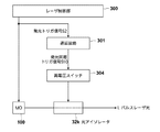
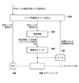
- FIG. 6 is a block diagram illustrating a schematic configuration of the laser apparatus according to the first embodiment.
- FIG. 7 is a flowchart showing the flow of control processing in the laser apparatus shown in FIG. FIG.
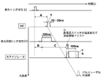
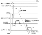
- FIG. 8 is a timing chart showing the generation timing of each signal in the laser apparatus shown in FIG.
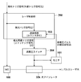
- FIG. 9 is a block diagram illustrating a schematic configuration of the laser apparatus according to the second embodiment.
- FIG. 10 is a flowchart showing the flow of control processing in the laser apparatus shown in FIG.
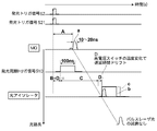
- FIG. 11 is a timing chart showing the generation timing of each signal in the laser apparatus shown in FIG.
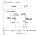
- FIG. 12 is a block diagram illustrating a schematic configuration of the laser apparatus according to the third embodiment.
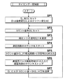
- FIG. 13 is a flowchart showing the flow of control processing in the laser apparatus shown in FIG.
- FIG. 14 is a timing chart showing the generation timing of each signal in the laser apparatus shown in FIG.
- FIG. 1 is a schematic side view showing the overall configuration of a typical extreme ultraviolet (EUV) light generation device.
- the EUV light generation apparatus shown in the figure is for supplying EUV light used as exposure light to the exposure apparatus 80. That is, the EUV light generation apparatus is configured by elements other than the exposure apparatus 80 and the exposure apparatus control unit 81 in FIG.
- the EUV light generation apparatus of this example is an apparatus that employs a laser generated plasma (LPP) system that generates EUV light by irradiating a target material with laser light to excite the target material.
- the EUV light generation apparatus includes an EUV chamber 1, an EUV light generation control unit 2, a laser device 3, a light transmission optical system (beam delivery system) 4, a droplet supply unit 5, and a droplet detection device 6. And the control system 50.
- LPP laser generated plasma
- the EUV chamber 1 is a chamber for generating EUV light therein, and is preferably a vacuum chamber.
- the EUV chamber 1 includes a stage 10, a first plate 11, a second plate 12 held in the EUV chamber 1 via the stage 10, and a highly reflective off-axis parabolic mirror held in the second plate 12. 13, a highly reflective flat mirror 14 similarly held by the second plate 12, and a window 15 for introducing laser light.
- the first plate 11 is provided with a through hole 16 for introducing laser light.
- the high reflection off-axis paraboloid mirror 13 and the high reflection flat mirror 14 constitute a laser condensing optical system 17 for condensing a pulsed laser beam L described later.
- the EUV chamber 1 further includes an EUV light collector mirror holder 20, an EUV light collector mirror 21 held by the EUV light collector mirror holder 20, a target receiver 22, and an EUV light pulse energy sensor 25.
- the EUV light collecting mirror 21 is a mirror having, for example, a spheroidal reflecting surface, and the first focal point is located in the plasma generation region 23 and the second focal point is located in the intermediate condensing point (IF) 24.
- IF intermediate condensing point
- the EUV light pulse energy sensor 25 is arranged to detect the energy of pulsed EUV light generated in the plasma generation region 23.
- the laser device 3 generates pulsed laser light L for exciting the target material.
- an oscillation amplification type laser apparatus master oscillator power amplifier type laser apparatus
- a combination of a YAG (Yttrium Aluminum Garnet) laser device that generates a pre-pulse laser beam and a CO 2 laser device that generates a main pulse laser beam can be applied as the laser device 3.
- other laser devices may be used as the laser device 3.
- the pulse laser beam L output from the laser device 3 is a laser beam having a pulse width of about several ns to several tens of ns and a frequency of about 10 kHz to 100 kHz, for example.
- the light transmission optical system 4 reflects the pulse laser light L output from the laser device 3 and changes the traveling direction thereof, and the pulse laser light L reflected by the first high reflection mirror 91. And a second highly reflective mirror 92 that reflects toward the window 15.
- the droplet supply unit 5 supplies a target material such as tin (Sn) or lithium (Li) used for generating EUV light into the EUV chamber 1 as a spherical droplet DL.
- the droplet supply unit 5 includes a pressure regulator 31, a tank 32 that stores a molten target material, a heater 33 that melts the target material, a nozzle 34 that discharges the molten target material, And a piezo element 35 that vibrates the side wall.
- the operation of the pressure regulator 31 is controlled by the control unit 51 of the control system 50.
- the droplet DL is generated intermittently and periodically and travels on the droplet trajectory Q in the EUV chamber 1.
- the droplet detection device 6 includes a light source unit 42 including a light source 40 such as a semiconductor laser that emits illumination light F having a visible wavelength, and an illumination optical system 41.
- the illumination optical system 41 condenses the illumination light F at a predetermined position P on the droplet trajectory Q. Therefore, if the droplet DL is present at the position P, the droplet DL partially blocks the illumination light F.
- the droplet detection device 6 includes a light receiving unit 45 including a light receiving optical system 43 that collects the illumination light F and a light sensor 44 that detects the collected illumination light F.
- the light receiving unit 45 is disposed so as to face the light source unit 42.
- the illumination optical system 41 includes, for example, a condenser lens. After being emitted from the light source 40, the illumination light F that has passed through the illumination optical system 41 is condensed at the position P.
- the light receiving optical system 43 also includes, for example, a condenser lens. The illumination light F diverged after being condensed at the position P is collected by the light receiving optical system 43 and enters the optical sensor 44.
- the target material in the tank 32 is heated by the heater 33 to a predetermined temperature equal to or higher than the melting point.
- a predetermined temperature equal to or higher than the melting point.
- the controller 51 may control the operation of the heater 33 to adjust the temperature.
- the operation of the pressure regulator 31 is controlled by the control unit 51 so that the pressure in the tank 32 is maintained at a pressure at which the jet of the melted target material is output from the nozzle 34 at a predetermined speed.
- the controller 51 applies a droplet supply signal, which is a voltage signal having a predetermined waveform, to the piezoelectric element 35 via a piezoelectric power supply (not shown). As a result, the piezoelectric element 35 vibrates and this vibration is applied to the nozzle 34. As described above, the jet output from the nozzle 34 is divided at a predetermined cycle by the vibration of the nozzle 34, and the droplet DL is intermittently supplied.
- the frequency of the vibration that is, the frequency of droplet generation is, for example, about 50 kHz to 100 kHz.
- the illumination light F output from the light source unit 42 of the droplet detection device 6 is received by the light receiving unit 45.
- the droplet DL generated and dropped as described above passes a predetermined position P in the trajectory Q, the illumination light F is blocked by the droplet DL.
- the received light amount of the illumination light F detected by the light receiving unit 45 decreases, and the output signal output from the light receiving unit 45 decreases in signal level corresponding to the decrease in the received light amount.
- the timing at which the droplet DL has passed the predetermined position P is indicated.
- the output signal output from the light receiving unit 45 is input to the control circuit 52 through the control unit 51 as the passage timing signal S1.
- the control circuit 52 includes a delay circuit 53 (see FIG. 2 described later). When the control circuit 52 detects a decrease in the signal level of the input passage timing signal S1, the control circuit 52 outputs the light emission trigger signal S2 with a predetermined time delay from the detection time point.
- the light emission trigger signal S2 is input to the laser device 3.
- the laser device 3 When the light emission trigger signal S2 is input, the laser device 3 outputs the pulsed laser light L as described in detail later.
- the pulse laser beam L is reflected by the first high reflection mirror 91 and the second high reflection mirror 92 of the light transmission optical system 4, then passes through the window 15 and enters the EUV chamber 1.
- the pulsed laser light L is reflected by the high reflection off-axis paraboloidal mirror 13 and the high reflection flat mirror 14 of the laser condensing optical system 17 and then passes through an opening provided in the central portion of the EUV light condensing mirror 21. Then, the light travels on the optical axis of the EUV light collector mirror 21.
- the pulsed laser light L is condensed in the plasma generation region 23 by the action of the high reflection off-axis parabolic mirror 13.
- the droplet DL that has reached the plasma generation region 23 can be turned into plasma upon irradiation with the condensed pulsed laser light L. Then, EUV light is generated from this plasma.
- the droplet DL that has not been irradiated with the pulse laser beam L is received by the target receiver 22.
- the droplet DL is periodically generated, and the pulsed laser light L is output every time the droplet DL is detected by the droplet detection device 6, so that EUV light is periodically generated.
- the EUV light thus periodically generated is collected at the intermediate condensing point 24 and then enters the exposure device 80.
- incident EUV light is used for semiconductor exposure or the like.
- the exposure device controller 81 of the exposure device 80 outputs a burst signal S4.
- the burst signal S4 is input to the control circuit 52 via the EUV light generation controller 2 and the controller 51.
- the light emission trigger signal S2 is output only when the burst signal S4 is input from the exposure apparatus controller 81 to the control circuit 52.
- the burst signal S4 is not input to the control circuit 52, the light emission trigger signal S2 is not output even if the passage timing signal S1 is input to the control unit 51. Accordingly, in this case, since the pulse laser beam L is not output, EUV light is not generated.
- the EUV light pulse energy sensor 25 shown in FIG. 1 detects the energy of pulsed EUV light generated in the plasma generation region 23, and outputs a pulse energy detection signal S5 indicating the energy.
- the pulse energy detection signal S5 is input to the control unit 51 of the control system 50.
- the control unit 51 calculates the target value of the energy of the pulsed laser light L based on the pulse energy of the EUV light indicated by the pulse energy detection signal S5, and inputs the target energy signal S3 indicating the target value to the laser device 3. To do. Thereby, the energy of the pulsed laser beam L output from the laser device 3 is set to the target value.
- the plasma generation region 23 may be moved in accordance with a command from the exposure apparatus 80.
- the time delay from when the control unit 51 detects a decrease in the signal level of the passage timing signal S1 to when the light emission trigger signal S2 is output is changed. You may let them.
- the stage 10 is operated, and the high reflection off-axis paraboloidal mirror 13 and the high reflection flat mirror 14 are passed through the second plate 12. May be moved in a plane perpendicular to the droplet trajectory Q.
- the EUV light generation control unit 2, the exposure apparatus control unit 81, the control system 50, the EUV light pulse energy sensor 25, and the droplet detection device 6 described above are collectively shown as a block diagram.
- the control system 50 includes the delay circuit 53 described above.
- the delay circuit 53 delays a predetermined time after the passage timing signal S1 is input to the control system 50, and outputs the light emission trigger signal S2.
- the pulse laser light L output from the laser device 3 that has received the light emission trigger signal S2 is generated.
- the droplet DL is set to be irradiated.
- the predetermined time includes, for example, the time Dt1 from when the droplet DL passes the position P until it reaches the plasma generation region 23, and the pulse laser beam L after the light emission trigger signal S2 is input to the laser device 3.
- the control unit 51 of the control system 50 sends data indicating the predetermined time to the delay circuit 53, and the delay time by the delay circuit 53 is set based on the data.
- FIG. 2 is a block diagram showing the basic configuration of the laser device 3.
- the laser device 3 includes a master oscillator 100 that emits pulsed laser light, n amplifiers 311, 312... 31 k... 31 n that sequentially amplify the laser light, and (n + 1) light. .., 32k, and 32n, and a laser controller 300.
- the master oscillator is denoted by MO
- the amplifier is denoted by PA.
- PA the optical shutter closest to the MO 100
- NPA 31 n and an nth optical shutter 32 n are sequentially arranged downstream of the 0th optical shutter 320.
- the k-th PA 31k and the k-th optical shutter 32k are provided as one set, and in addition to the 0-th optical shutter 320, n sets are provided.
- a CO 2 laser oscillator including a Q switch, a quantum cascade laser (QCL) that oscillates in an amplification wavelength region of a CO 2 laser gas, or the like can be suitably used.
- the MO 100 receives the light emission trigger signal S2, the MO 100 outputs the pulsed laser light L.
- the pulsed laser light L may be linearly polarized light.
- PA 311, 312... 31 k... 31 n may be a discharge excitation type amplifier including a CO 2 laser gas arranged on the optical path of the pulse laser beam L output from the MO 100. Further, PA 311, 312... 31 k... 31 n may include a CO 2 laser gas, a pair of electrodes, and a power source that performs high-frequency discharge between these electrodes.
- the CO 2 laser gas may be pumped so that a predetermined excitation intensity is obtained in each of the PAs 311, 312,.
- the PAs 311, 312,... 31 k, 31 n include an optical resonator, an EO Pockels cell, a polarizer, May be a regenerative amplifier.
- optical shutters 320, 321, 322... 32 k... 32 n each have a function of being opened only for a short period of time during which pulsed laser light passes. The function of this optical shutter will be described in detail later.
- the pulsed laser beams that have passed through the optical shutters 320, 321, 322,... 32k,... 32n are sequentially amplified by PAs 311, 312,. It is done.
- the optical shutters 320, 321, 322... 32 k... 32 n may include an EO Pockels cell or may include an EO Pockels cell and two polarizers.
- the optical shutter having low resistance to the pulsed laser light L is positioned at the upstream side where the pulse energy of the pulsed laser light L is relatively low, such as the 0th optical shutter 320 shown in FIG. It is preferable to arrange between 1PA311.
- FIG. 3 shows an example of an optical shutter.
- one optical shutter is shown, which is representatively shown as an optical shutter 32k.
- the optical shutter 32k includes a first polarizer 341 and a second polarizer 342 that are disposed apart from each other, an EO Pockels cell 340 disposed between them, and a second polarizer 342 and an EO Pockels cell.
- ⁇ / 2 plate (half-wave plate) 343 disposed between 340 and 340.
- the EO Pockels cell 340 includes, for example, electrodes 340a and 340b and an electro-optic (EO) crystal 340c disposed therebetween.
- EO electro-optic
- a high voltage of a predetermined value can be applied to the electro-optic crystal 340c from the high voltage switch 304 controlled by a control circuit (not shown) via the electrodes 340a and 340b.
- the electro-optic crystal 340c rotates the linear polarization direction of the passing pulse laser beam L by 90 °.
- FIG. 3 along the optical path of the pulse laser beam L, an arrow extending vertically and a circle mark are attached.
- the former arrow indicates that the linear polarization direction of the pulse laser beam L is parallel to the paper surface (vertical direction), and the latter circle indicates that the linear polarization direction of the pulse laser beam L is perpendicular to the paper surface.
- pulsed laser light L that passes through the optical shutter 32k from left to right in FIG. 3, particularly pulsed laser light L linearly polarized in the vertical direction in FIG. 3 is used.
- the linearly polarized pulsed laser light L is transmitted through the second polarizer 342, and the polarization direction is rotated by 90 ° at the ⁇ / 2 plate 343.
- the pulsed laser light L whose linear polarization direction is perpendicular to the paper surface is reflected by the first polarizer 341 while maintaining the polarization direction as it is when the high voltage is not applied to the electro-optic crystal 340c. Therefore, it cannot pass through the optical shutter 32k.
- the pulsed laser light L passes through the electro-optic crystal 340c, so that the linear polarization direction returns to the direction parallel to the paper surface. 341 is transmitted through the optical shutter 32k.
- the optical shutter 32k opens and closes according to ON / OFF of high voltage application. Further, the optical shutter 32k of this example also opens and closes in response to the pulsed laser light L that attempts to pass through the optical shutter 32k from right to left in FIG.
- the optical shutter has a function of passing the pulsed laser light L from the left to the right in FIG. 2 as described above and blocking the light from the right to the left in FIG. 2 when a high voltage is applied.
- An isolator may be used.
- a part of the pulsed laser light L may be reflected by the target.
- a so-called self-excited oscillation phenomenon may occur in which spontaneously emitted light emitted from each of a plurality of PAs is amplified by other PAs.
- the self-oscillation light generated by this self-oscillation and the light reflected by the above-mentioned target may be returned light, and the optical path of the pulsed laser light L may flow backward to the MO 100 side.
- the optical isolator described above it is possible to suppress the laser device from being damaged by such return light, and to stabilize the output of the pulsed laser light L.
- a part of the pulsed laser light L is reflected by the beam splitter 303, and the remainder passes through the beam splitter 303 and enters the light transmission optical system 4 shown in FIG.
- the pulsed laser light L reflected by the beam splitter 303 enters the pulse energy sensor 302.
- the pulse energy sensor 302 detects the energy of the pulse laser beam L and inputs an energy detection signal to the laser control unit 300. Based on this energy detection signal, the laser control unit 300 controls the output of the MO 100 so that the target energy indicated by the target energy signal S3 shown in FIG. 1 is obtained.
- the beam splitter 303 is not limited to the position shown in FIG. 2 and may be disposed upstream of the position in the traveling direction of the pulsed laser light L.
- the operation of the laser control unit 300 is controlled by the control unit 51 of the control system 50.
- a high voltage is not applied to the optical shutters 320, 321, 322,. That is, only when the burst signal S4 is input to the control unit 51, if this high voltage is applied, the pulse laser beam L can pass through the optical shutters 320, 321, 322,. Become.
- the respective optical shutters are matched with the timing at which the pulse laser beam L passes through each optical shutter. May be set to an open state.
- FIG. 4 shows a configuration for applying the high voltage, and this configuration will be described in detail below.
- one optical shutter is typically shown as an optical shutter 32k, and the configuration around the optical shutter 32k will be described.
- the configuration shown in FIG. 4 may be provided for each optical shutter.
- the laser apparatus shown in FIG. 4 includes a laser control unit 300, an MO 100, an optical shutter 32k, a delay circuit 301, and a high voltage switch 304.
- the light emission trigger signal S ⁇ b> 2 that has passed through the laser controller 300 can be input to the MO 100 and the delay circuit 301.
- the optical shutter 32k includes an EO Pockels cell 340 as shown in FIG. 3, for example.
- the high voltage switch 304 includes, for example, a semiconductor switch and is connected to a high voltage source (not shown).
- the MO 100 described above When receiving the light emission trigger signal S2, the MO 100 described above outputs a pulsed laser beam.
- This pulse laser beam is amplified by, for example, a PA (not shown) as shown in FIG. 2, and a high-intensity pulse laser beam L is obtained.
- the delay circuit 301 When the light emission trigger signal S2 is input to the delay circuit 301, the delay circuit 301 outputs a light emission synchronization trigger signal S10 synchronized with the light emission trigger signal S2.
- the light emission synchronization trigger signal S10 is input to the high voltage switch 304.
- the high voltage switch 304 performs a switching operation when the light emission synchronization trigger signal S10 is input, and applies a predetermined high voltage from the high voltage source to the optical shutter 32k.
- the light emission synchronization trigger signal S10 is output from the delay circuit 301 after being delayed from the light emission trigger signal S2 by a predetermined time so that a high voltage is applied to the optical shutter 32k in accordance with the timing when the pulse laser light L passes through the optical shutter 32k. Is done.
- the optical shutter 32k as an optical switch allows the pulsed laser light L to pass while the high voltage is applied.
- FIG. 5 is a timing chart showing the timing at which each signal in the configuration of FIG. 4 is generated together with the traveling position of the pulsed laser light L.
- the horizontal axis in FIG. 5 indicates the time indicated by, for example, s (seconds).
- the waveforms of the emission trigger signal S2, the pulse laser beam L output from the MO100, the emission synchronization trigger signal S10, and the high voltage applied to the optical shutter 32k are sequentially applied from the top to the bottom.
- the generation timing The position on the downward arrow drawn to the vertical axis position corresponds to the optical path length from the MO 100 to the optical shutter 32k side.
- the pulse width (full value full width) of the pulsed laser light L is about 10 to 20 ns.
- the pulse width of the light emission synchronization trigger signal S10 is about 100 ns.
- the waveform of the high voltage applied to the optical shutter 32k is indicated by b or c in FIG.
- the pulse width of this high voltage is about 100 ns corresponding to the pulse width of the light emission synchronization trigger signal S10.
- the time from the rise of the light emission trigger signal S2 to the start of the high voltage application It needs to be constant. That is, in FIG. 5, if this time is always (B + C) and the waveform of the high voltage is as shown by the broken line b, the pulse laser beam L passes through the optical shutter 32k over the entire width of the pulse width. . Further, unnecessary light emission components present at the pulse bottom of the pulse laser beam L can also be removed by the optical shutter 32k.
- the time from when the light emission synchronization trigger signal S10 is received to when the high voltage application is started may fluctuate due to a temperature change. If there is this time variation, so-called time drift, the waveform of the high voltage shown in FIG. 5 becomes, for example, a solid line c, and the time from the rise of the light emission trigger signal S2 to the start of high voltage application can be changed to (B + C + D). .
- D represents the amount of fluctuation from the original value (B + C) of the time.
- the pulse laser beam L can only pass through a part of the pulse width through the optical shutter 32k, it is attenuated when it passes through the optical shutter 32k.
- Embodiment 1 3.1 Configuration of Embodiment 1
- a laser apparatus according to Embodiment 1 will be described with reference to FIGS. 6 to 8, the same elements as those shown in FIGS. 1 to 5 are denoted by the same reference numerals, and description thereof will be omitted unless necessary (the same applies hereinafter).
- the laser device of the first embodiment can also be applied as the laser device 3 shown in FIGS.
- FIG. 6 is a block diagram illustrating a basic configuration of the laser apparatus according to the first embodiment. This laser device differs from the laser device shown in FIG. 4 in that a high voltage monitor 151 is added and a delay circuit 153 including a counter is used in place of the delay circuit 301.
- This counter counts the elapsed time in units much shorter than the variation D (see FIG. 5) of the time from when the high voltage switch 304 receives the light emission synchronization trigger signal S10 until the high voltage application is started.
- the high voltage monitor 151 detects a high voltage pulse output from the high voltage switch 304 and inputs a detection signal S6 to the delay circuit 153.
- FIG. 7 shows a control flow in which the timing at which a pulsed high voltage is applied to the optical shutter 32k coincides with the timing at which the pulsed laser light L passes through the optical shutter 32k.
- FIG. 8 is a timing chart showing the timing at which each signal is generated under this control, together with the traveling position of the pulse laser beam L.
- the display method of FIG. 8 is the same as that of FIG. 5 described above. The above control will be described below with reference to FIGS.
- the delay circuit 153 first sets the value of Di-1 stored therein to 0 (zero) in step SP1.
- D represents the above-described time variation within the time from when the high voltage switch 304 receives the light emission synchronization trigger signal S10 until the high voltage application starts. More specifically, this time is supposed to be a constant time C, but D is a time to be added or subtracted.
- the processing from step SP2 to step SP7 is repeated thereafter.
- the above i indicates the order of this iterative process.
- D i represents the time change when this order is the i-th. Since the value of i is first set to 1, the value of D i ⁇ 1 is set to 0 as described above. The value of i is incremented by “1” every time the process returns from step SP7 to step SP2.
- the delay circuit 153 next sets the count value of its counter to 0 (zero) in step SP2.
- the delay circuit 153 receives the light emission trigger signal S2 shown in FIGS. 1 and 2 as an external trigger signal, and outputs the light emission trigger signal S21 after a predetermined time when it is received.
- the light emission trigger signal S21 is simultaneously input to the MO 100 and the delay circuit 153 as shown in FIG.
- the delay circuit 153 starts counting by the counter in the next step SP4.
- step SP5 the delay circuit 153 outputs the light emission synchronization trigger signal S10 when the count value becomes (BD i-1 ), whereby the high voltage switch 304 starts the switching operation, and the high voltage pulse is applied to the optical shutter 32k. Is applied.
- the light emission synchronization trigger signal S10 acts as a switching signal for starting the operation of the high voltage switch 304.
- the optical shutter 32k is in a state where light can pass while the high voltage pulse is applied, and the pulsed laser light L passes through the optical shutter 32k.
- B is a target value of the delay time from when the light emission trigger signal S21 is input to the delay circuit 153 to when the light emission synchronization trigger signal S10 is output, as shown in FIG.
- the actual delay time in the first embodiment is (BD i-1 ).
- C which will be described later, is a target value of the time from when the light emission synchronization trigger signal S10 rises until the high voltage pulse starts to be applied to the optical shutter 32k.
- These target values B and C are predetermined constant values, and are stored in the delay circuit 153, for example.
- the high voltage monitor 151 shown in FIG. 6 detects the high voltage pulse output from the high voltage switch 304 and inputs the detection signal S6 to the delay circuit 153.
- the delay circuit 153 stops the time measurement by the counter (step SP6 in FIG. 7).
- Delay circuit 153 thus the counting by the counter is stopped, then in step SP7, adds the correction value ⁇ D to the value of D i-1, and sets the value after the addition as new D i-1.
- the correction value ⁇ D (count value when the time measurement is stopped ⁇ (BD i ⁇ 1 + C)).
- a delay time from when the light emission trigger signal S21 is output until when the light emission synchronization trigger signal S10 is output. Becomes (BD i-1 ). That is, in the i-th iterative process, this delay time is a time obtained by subtracting the time fluctuation (D i-1 ) measured in the previous time, that is, the i ⁇ 1-th iterative process, from the target value B. Therefore, as indicated by a solid line b in FIG. 8, it is possible to make the timing at which the pulsed high voltage is applied to the optical shutter 32k coincide with the timing at which the pulsed laser light L passes through the optical shutter 32k.
- the pulse laser beam L passes through the optical shutter 32k over the entire width of the pulse width, the pulse laser beam L is suppressed from being attenuated during this passage. Further, unnecessary light emission components present at the pulse bottom of the pulse laser beam L can also be removed by the optical shutter 32k.
- FIG. 9 is a block diagram illustrating a basic configuration of a laser apparatus according to the second embodiment.
- this laser device uses a laser control unit 330 including a counter instead of the laser control unit 300, and instead of the delay circuit 153, The difference is that a delay circuit 253 that does not include a counter is used.
- the counter included in the laser control unit 330 is an elapsed time in a unit that is extremely shorter than the time variation D (see FIG.
- the high voltage monitor 151 detects a high voltage pulse output from the high voltage switch 304 and inputs a detection signal S ⁇ b> 6 to the laser control unit 330.
- FIG. 10 shows the flow of this control, that is, the control for making the timing at which the pulsed high voltage is applied to the optical shutter 32k coincide with the timing at which the pulse laser beam L passes through the optical shutter 32k.
- FIG. 11 is a timing chart showing the timing at which each signal is generated under this control, together with the traveling position of the pulse laser beam L.
- the display method of FIG. 11 is the same as that of FIG. 5 described above.
- the control by the laser controller 330 will be described with reference to FIGS. 10 and 11.
- the laser controller 330 When the control shown in FIG. 10 starts, the laser controller 330 first sets the value of D i ⁇ 1 stored therein to 0 (zero) in step SP11.
- the meanings of D, i, and D i-1 are the same as those in the first embodiment.
- the processing from step SP12 to step SP18 is repeated thereafter.
- the value of i is incremented by “1” every time the process returns from step SP18 to step SP12.
- the laser controller 330 sets the count value of the counter to 0 (zero).
- the laser controller 330 receives the light emission trigger signal S2 shown in FIGS. 1 and 2 as an external trigger signal.
- the laser controller 330 receives the light emission trigger signal S2 in step SP13, and at the same time, starts measuring time by a counter in step SP14.
- step SP15 the laser controller 330 outputs the second light emission trigger signal S22 when the count value reaches (t0 ⁇ D i ⁇ 1 ), and then in step SP16, the count value becomes t0.
- the first light emission trigger signal S21 is output.
- t0 is a predetermined value, and this value is the first delay time in the present disclosure.
- the value of t0 is stored in the laser control unit 330. As shown in FIG. 9, the first light emission trigger signal S 21 is input to the MO 100, and the second light emission trigger signal S 22 is input to the delay circuit 253.
- the MO 100 shown in FIG. 9 When the MO 100 shown in FIG. 9 receives the first light emission trigger signal S21, the MO 100 outputs the pulsed laser light L.
- the delay circuit 253 receives the second light emission trigger signal S22, as shown in FIG. 11, the delay circuit 253 delays by the time B described below and outputs the light emission synchronization trigger signal S10 as a switching signal. This time B is the second delay time in the present disclosure.
- the light emission synchronization trigger signal S10 is input to the high voltage switch 304 shown in FIG. When the light emission synchronization trigger signal S10 is input, the high voltage switch 304 starts a switching operation and applies a high voltage pulse to the optical shutter 32k.
- the timing of applying the high voltage pulse is originally the timing when the target value C has elapsed since the light emission synchronization trigger signal S10 rises. However, if there is a fluctuation in the time from when the high voltage switch 304 receives the light emission synchronization trigger signal S10 to when the high voltage application is started, the actual timing is (C + D) after the light emission synchronization trigger signal S10 rises. It is the timing when elapses.
- D is the time for the variation.
- D i shown in FIG. 11 and the like indicates the amount of fluctuation when the above iterative process is the i-th.
- the target values B and C and the value of t0 are stored in the laser control unit 330, for example.
- the value of the target value B is also stored in the delay circuit 253.
- the high voltage monitor 151 illustrated in FIG. 9 detects a high voltage pulse output from the high voltage switch 304 and inputs a detection signal S6 to the laser control unit 330.
- the laser controller 330 stops the time counting by the counter (step SP17 in FIG. 10).
- the laser control unit 330 thus the timing is stopped by the counter, then in step SP18, by adding the correction value ⁇ D to the value of D i-1, and stores the value after the addition as a new D i-1 .
- the correction value ⁇ D (count value when the time measurement is stopped ⁇ (t0 ⁇ D i ⁇ 1 + B + C)).
- Embodiment 2 By performing the processing described above, as shown in FIG. 11, from the output of the first light emission trigger signal S21 to the output of the light emission synchronization trigger signal S10.
- the delay time is (BD i-1 ). That is, in the i-th iterative process, this delay time is a time obtained by subtracting the time fluctuation (D i-1 ) measured in the previous time, that is, the i ⁇ 1-th iterative process, from the target value B. Therefore, as indicated by a solid line b in FIG. 11, the timing at which the pulsed high voltage is applied to the optical shutter 32k can be matched with the timing at which the pulsed laser light L passes through the optical shutter 32k.
- the pulse laser beam L passes through the optical shutter 32k over the entire width of the pulse width, the pulse laser beam L is suppressed from being attenuated during this passage. Further, unnecessary light emission components present at the pulse bottom of the pulse laser beam L can also be removed by the optical shutter 32k.
- FIG. 12 is a block diagram illustrating a basic configuration of a laser apparatus according to the third embodiment.
- This laser device is different from the laser device according to the first embodiment shown in FIG. 6 in that a laser control unit 350 including a delay circuit 153 is used instead of the laser control unit 300.
- the delay circuit 153 has basically the same configuration and function as the delay circuit 153 shown in FIG. 6, and includes the above-described counter.
- FIG. 13 shows a flow of this control, that is, a control for matching the timing at which a pulsed high voltage is applied to the optical shutter 32k with the timing at which the pulsed laser light L passes through the optical shutter 32k.
- FIG. 14 is a timing chart showing the timing at which each signal is generated under this control, together with the traveling position of the pulse laser beam L.
- the display method of FIG. 14 is the same as that of FIG. 5 described above.
- the control by the laser control unit 350 will be described with reference to FIGS. 13 and 14.
- the control shown in FIG. 13 differs from the control in the first embodiment shown in FIG. 7 only in the reception and output of the light emission trigger signal, and the operation of the delay circuit 153 included in the laser control unit 350 is also the first embodiment.
- the operation is the same as in FIG. That is, steps SP21 and 22 shown in FIG. 13 are the same as steps SP1 and SP2 in FIG. 7, and steps SP26, 27 and 28 shown in FIG. 13 are the same as steps SP5, 6 and 7 in FIG. .
- the laser control unit 350 receives the light emission trigger signal S2 which is an external trigger signal in step SP23, starts counting the counter included in itself in step SP24, and at the same time outputs the light emission trigger signal S21 in step SP25. Output.
- the switching signal is delayed by a delay time (BD i-1 ).
- a certain light emission synchronization trigger signal S10 is output.
- This delay time (BD i-1 ) is the third delay time in the present disclosure.
- Embodiment 3 As described above, according to Embodiment 3, the same operation / effect as in Embodiment 1 can be obtained. That is, also in the third embodiment, as indicated by the solid line b in FIG. 14, the timing at which the pulsed high voltage is applied to the optical shutter 32k can be matched with the timing at which the pulsed laser light L passes through the optical shutter 32k. It becomes possible. Therefore, since the pulse laser beam L passes through the optical shutter 32k over the entire width of the pulse width, attenuation of the pulse laser beam L during this passage is suppressed. Further, unnecessary light emission components present at the pulse bottom of the pulse laser beam L can also be removed by the optical shutter 32k.
Landscapes
- Physics & Mathematics (AREA)
- Electromagnetism (AREA)
- Engineering & Computer Science (AREA)
- Optics & Photonics (AREA)
- Plasma & Fusion (AREA)
- General Physics & Mathematics (AREA)
- Microelectronics & Electronic Packaging (AREA)
- Lasers (AREA)
Abstract
【課題】マスターオシレータから発せられたパルスレーザ光を、高電圧パルスが印加されて開く光シャッタに通すレーザ装置において、高電圧パルスの印加タイミングを、光シャッタにパルスレーザ光が到達するタイミングと一致させる。 【解決手段】レーザ装置は、発光トリガ信号(S21)に基づいてパルスレーザ光(L)を出力するマスターオシレータ(100)、発光トリガ信号(S21)の受信時から所定の遅延時間を置いてスイッチング信号(S10)を生成する遅延回路(153)、スイッチング信号(S10)に基づいて高電圧パルスを生成する高電圧スイッチ(304)、パルスレーザ光(L)の光路上に位置し高電圧パルスに基づいて駆動される光シャッタ(32k)、および高電圧パルスを検出して高電圧パルス検知信号(S6)を遅延回路(153)に送信する高電圧モニタ(151)を含む。遅延回路(153)は、発光トリガ信号(S21)と高電圧パルス検知信号(S6)とに基づいて遅延時間を決定する。
Description
本開示はレーザ装置および、このレーザ装置を用いる極端紫外光生成装置に関する。
近年、半導体プロセスの微細化に伴って、半導体プロセスの光リソグラフィにおける転写パターンの微細化が急速に進展している。次世代においては、20nm以下の微細加工が要求されるようになる。このため、例えば20nm以下の微細加工の要求に応えるべく、波長13.5nmの極端紫外(EUV)光を生成する極端紫外光生成装置と縮小投影反射光学系(Reduced Projection Reflective Optics)とを組み合わせた露光装置の開発が期待されている。
EUV光生成装置としては、ターゲット物質にパルスレーザ光を照射することによって生成されるプラズマが用いられるLPP(Laser Produced Plasma)式の装置と、放電によって生成されるプラズマが用いられるDPP(Discharge Produced Plasma)式の装置と、電子加速器から出力される電子を用いた自由電子レーザ(Free Electron Laser)装置の3種類の装置が提案されている。
本開示の一態様によるレーザ装置は、発光トリガ信号を生成するレーザ制御部、レーザ制御部から送信された発光トリガ信号に基づいてパルスレーザ光を出力するマスターオシレータ、レーザ制御部から送信された発光トリガ信号を受信し、この受信時から所定の遅延時間を置いてスイッチング信号を生成する遅延回路、遅延回路から送信されたスイッチング信号に基づいて高電圧パルスを生成する高電圧スイッチ、マスターオシレータから出力されたパルスレーザ光の光路上に位置し、高電圧スイッチから出力された高電圧パルスに基づいて駆動される光シャッタ、および高電圧スイッチから出力された高電圧パルスを検出し、高電圧パルス検知信号を遅延回路に送信する高電圧モニタを含み、遅延回路は、発光トリガ信号と高電圧パルス検知信号とに基づいて遅延時間を決定する。
本開示の別の態様によるレーザ装置は、外部トリガ信号を受信し、この受信時から第1の遅延時間を置いて第1の発光トリガ信号を生成し、外部トリガ信号に基づいて第2の発光トリガ信号を生成するレーザ制御部、レーザ制御部から送信された第1の発光トリガ信号に基づいてパルスレーザ光を出力するマスターオシレータ、レーザ制御部から送信された第2の発光トリガ信号を受信し、この受信時から第2の遅延時間を置いてスイッチング信号を生成する遅延回路、遅延回路から送信されたスイッチング信号に基づいて高電圧パルスを生成する高電圧スイッチ、マスターオシレータから出力されたパルスレーザ光の光路上に位置し、高電圧スイッチから出力された高電圧パルスに基づいて駆動される光シャッタ、および高電圧スイッチから出力された高電圧パルスを検出し、高電圧パルス検知信号をレーザ制御部に送信する高電圧モニタを含み、レーザ制御部は、外部トリガ信号と高電圧パルス検知信号とに基づいて遅延時間を決定する。
本開示のさらに別の態様によるレーザ装置は、受信した外部トリガ信号に基づいて発光トリガ信号を生成し、外部トリガ信号の受信時から第3の遅延時間を置いてスイッチング信号を生成するレーザ制御部、レーザ制御部から送信された発光トリガ信号に基づいてパルスレーザ光を出力するマスターオシレータ、レーザ制御部から送信されたスイッチング信号に基づいて高電圧パルスを生成する高電圧スイッチ、マスターオシレータから出力されたパルスレーザ光の光路上に位置し、高電圧スイッチから出力された高電圧パルスに基づいて駆動される光シャッタ、および高電圧スイッチから出力された高電圧パルスを検出し、高電圧パルス検知信号をレーザ制御部に送信する高電圧モニタを含み、レーザ制御部は、外部トリガ信号と高電圧パルス検知信号とに基づいて第3の遅延時間を決定する。
本開示のいくつかの実施形態を、単なる例として、添付の図面を参照して以下に説明する。
図1は、典型的なEUV光生成装置の全体構成を示す概略側面図である。
図2は、図1に示すEUV光生成装置の要部を概略的に示すブロック図である。
図3は、光シャッタの一例を示す概略図である。
図4は、比較例としてのレーザ装置の概略構成を示すブロック図である。
図5は、図4に示すレーザ装置における各信号の発生タイミングを示すタイミングチャートである。
図6は、実施形態1に係るレーザ装置の概略構成を示すブロック図である。
図7は、図6に示すレーザ装置における制御処理の流れを示すフローチャートである。
図8は、図6に示すレーザ装置における各信号の発生タイミングを示すタイミングチャートである。
図9は、実施形態2に係るレーザ装置の概略構成を示すブロック図である。
図10は、図9に示すレーザ装置における制御処理の流れを示すフローチャートである。
図11は、図9に示すレーザ装置における各信号の発生タイミングを示すタイミングチャートである。
図12は、実施形態3に係るレーザ装置の概略構成を示すブロック図である。
図13は、図12に示すレーザ装置における制御処理の流れを示すフローチャートである。
図14は、図12に示すレーザ装置における各信号の発生タイミングを示すタイミングチャートである。
<目次>
1.EUV光生成装置の全体説明
1.1 構成
1.2 動作
2.比較例
2.1 構成
2.2 動作
2.3 課題
3.実施形態1
3.1 実施形態1の構成
3.2 実施形態1の動作
3.3 実施形態1の作用・効果
4.実施形態2
4.1 実施形態2の構成
4.2 実施形態2の動作
4.3 実施形態2の作用・効果
5.実施形態3
5.1 実施形態3の構成
5.2 実施形態3の動作
5.3 実施形態3の作用・効果
1.EUV光生成装置の全体説明
1.1 構成
1.2 動作
2.比較例
2.1 構成
2.2 動作
2.3 課題
3.実施形態1
3.1 実施形態1の構成
3.2 実施形態1の動作
3.3 実施形態1の作用・効果
4.実施形態2
4.1 実施形態2の構成
4.2 実施形態2の動作
4.3 実施形態2の作用・効果
5.実施形態3
5.1 実施形態3の構成
5.2 実施形態3の動作
5.3 実施形態3の作用・効果
以下、本開示の実施形態について、図面を参照しながら詳しく説明する。以下に説明される実施形態は、本開示のいくつかの例を示すものであって、本開示の内容を限定するものではない。また、各実施形態で説明される構成および動作の全てが本開示の構成および動作として必須であるとは限らない。なお、同一の構成要素には同一の参照符号を付して、重複する説明を省略する。
1.EUV光生成装置の全体説明
1.1 構成
図1は、典型的な極端紫外(EUV)光生成装置の全体構成を示す概略側面図である。同図に示すEUV光生成装置は、露光装置80に露光光として利用されるEUV光を供給するためのものである。すなわち、図1中の、露光装置80および露光装置制御部81以外の要素により、EUV光生成装置が構成されている。本例のEUV光生成装置は、レーザ光をターゲット物質に照射してターゲット物質を励起することによりEUV光を発生させる、レーザ生成プラズマ(LPP)方式を採用した装置である。このEUV光生成装置は、EUVチャンバ1と、EUV光生成制御部2と、レーザ装置3と、送光光学系(ビームデリバリシステム)4と、ドロップレット供給部5と、ドロップレット検出装置6と、制御システム50とを含む。
1.1 構成
図1は、典型的な極端紫外(EUV)光生成装置の全体構成を示す概略側面図である。同図に示すEUV光生成装置は、露光装置80に露光光として利用されるEUV光を供給するためのものである。すなわち、図1中の、露光装置80および露光装置制御部81以外の要素により、EUV光生成装置が構成されている。本例のEUV光生成装置は、レーザ光をターゲット物質に照射してターゲット物質を励起することによりEUV光を発生させる、レーザ生成プラズマ(LPP)方式を採用した装置である。このEUV光生成装置は、EUVチャンバ1と、EUV光生成制御部2と、レーザ装置3と、送光光学系(ビームデリバリシステム)4と、ドロップレット供給部5と、ドロップレット検出装置6と、制御システム50とを含む。
上記EUVチャンバ1は、その内部でEUV光を生成するためのチャンバであり、好ましくは真空チャンバとされる。EUVチャンバ1は、ステージ10と、第1プレート11と、ステージ10を介してEUVチャンバ1に保持された第2プレート12と、この第2プレート12に保持された高反射軸外放物面ミラー13と、同じく第2プレート12に保持された高反射平面ミラー14と、レーザ光導入用のウインドウ15とを含む。なお、上記第1プレート11には、レーザ光導入用の貫通孔16が設けられている。上記高反射軸外放物面ミラー13および高反射平面ミラー14は、後述するパルスレーザ光Lを集光するためのレーザ集光光学系17を構成している。
EUVチャンバ1はさらに、EUV光集光ミラーホルダ20と、このEUV光集光ミラーホルダ20に保持されたEUV光集光ミラー21と、ターゲット受け22と、EUV光パルスエネルギセンサ25とを含む。EUV光集光ミラー21は、例えば回転楕円面形状の反射面を有するミラーであり、第1の焦点がプラズマ生成領域23に位置し、第2の焦点が中間集光点(IF)24に位置するように配置されている。EUV光パルスエネルギセンサ25は、プラズマ生成領域23において発生するパルス状のEUV光のエネルギを検出するように配置されている。
レーザ装置3は、ターゲット物質を励起するためのパルスレーザ光Lを発生させる。このレーザ装置3としては、一例として発振増幅型レーザ装置(master oscillator power amplifier type laser apparatus)が適用される。あるいは、レーザ装置3として、プリパルスレーザビームを発生させるYAG(Yttrium Aluminum Garnet)レーザ装置と、メインパルスレーザビームを発生させるCO2レーザ装置との組合せ等も適用可能である。さらに、レーザ装置3として、その他のレーザ装置が用いられてもよい。このレーザ装置3から出力されるパルスレーザ光Lは、例えばパルス幅が数ns~数十ns程度、周波数が10kHz~100kHz程度のレーザ光である。
送光光学系4は、レーザ装置3から出力されたパルスレーザ光Lを反射させてその進行方向を変える第1高反射ミラー91と、この第1高反射ミラー91で反射したパルスレーザ光Lを上記ウインドウ15に向けて反射させる第2高反射ミラー92とを含む。
ドロップレット供給部5は、EUV光を発生させるために用いられるスズ(Sn)やリチウム(Li)等のターゲット物質を、球状のドロップレットDLとしてEUVチャンバ1内に供給する。このドロップレット供給部5は、圧力調節器31と、溶融した状態のターゲット物質を蓄えるタンク32と、ターゲット物質を溶融させるヒータ33と、溶融状態のターゲット物質を吐出させるノズル34と、ノズル34の側壁を振動させるピエゾ素子35とを含む。なお、上記圧力調節器31の動作は、制御システム50の制御部51によって制御される。上記ドロップレットDLは断続的かつ周期的に生成され、EUVチャンバ1内においてドロップレット軌道Q上を進行する。
ドロップレット検出装置6は、例えば可視域の波長の照明光Fを発する半導体レーザ等の光源40と、照明光学系41とを含む光源部42を備えている。照明光学系41は、上記ドロップレット軌道Q上の所定の位置Pに照明光Fを集光する。そこで、この位置PにドロップレットDLが存在すれば、そのドロップレットDLが照明光Fを一部遮ることになる。またドロップレット検出装置6は、上記照明光Fを集光する受光光学系43と、集光された照明光Fを検出する光センサ44とを含む受光部45を備えている。受光部45は、光源部42と対向する状態に配置されている。
上記照明光学系41は例えば集光レンズを含む。光源40から発せられた後、この照明光学系41を経た照明光Fは、上記位置Pにおいて集光する。一方受光光学系43も例えば集光レンズを含む。上記位置Pにおいて集光した後に発散した照明光Fは、受光光学系43により集光されて光センサ44に入射する。
1.2 動作
上記の構成において、タンク32中のターゲット物質は、ヒータ33によって融点以上の所定温度に加熱される。例えばターゲット物質がSnである場合、Snはその融点(232℃)以上の250~290℃の温度範囲に加熱される。この加熱を行うに当たっては、制御部51によりヒータ33の動作を制御して、温度調節を行ってもよい。また、制御部51により圧力調節器31の動作が制御されて、タンク32内の圧力が、融解したターゲット物質のジェットがノズル34から所定の速度で出力する圧力に維持される。そして制御部51により、図示外のピエゾ電源を介してピエゾ素子35に、所定波形の電圧信号であるドロップレット供給信号が印加される。それによりピエゾ素子35が振動して、この振動がノズル34に加えられる。以上により、ノズル34から出力される上記ジェットがノズル34の振動によって所定周期で分断され、ドロップレットDLが断続的に供給されるようになる。上記振動の周波数、すなわちドロップレット生成の周波数は、例えば50kHz~100kHz程度とされる。
上記の構成において、タンク32中のターゲット物質は、ヒータ33によって融点以上の所定温度に加熱される。例えばターゲット物質がSnである場合、Snはその融点(232℃)以上の250~290℃の温度範囲に加熱される。この加熱を行うに当たっては、制御部51によりヒータ33の動作を制御して、温度調節を行ってもよい。また、制御部51により圧力調節器31の動作が制御されて、タンク32内の圧力が、融解したターゲット物質のジェットがノズル34から所定の速度で出力する圧力に維持される。そして制御部51により、図示外のピエゾ電源を介してピエゾ素子35に、所定波形の電圧信号であるドロップレット供給信号が印加される。それによりピエゾ素子35が振動して、この振動がノズル34に加えられる。以上により、ノズル34から出力される上記ジェットがノズル34の振動によって所定周期で分断され、ドロップレットDLが断続的に供給されるようになる。上記振動の周波数、すなわちドロップレット生成の周波数は、例えば50kHz~100kHz程度とされる。
一方、ドロップレット検出装置6の光源部42から出力された照明光Fは、受光部45に受光される。そして、上述のように生成されて落下するドロップレットDLが、その軌道Qにおいて所定の位置Pを通過すると、ドロップレットDLにより照明光Fが遮られる。そのとき、受光部45が検出する照明光Fの受光量が低下し、受光部45が出力する出力信号は、この受光量の低下に対応して信号レベルが低下する。信号レベルがある閾値電圧より小さくなるときが、ドロップレットDLが上記所定の位置Pを通過したタイミングを示すものとなる。受光部45が出力する出力信号は、通過タイミング信号S1として、制御部51を介して制御回路52に入力される。制御回路52は遅延回路53(後述の図2参照)を含む。制御回路52は、入力された通過タイミング信号S1の信号レベル低下を検出すると、その検出時点から所定の時間遅延させて発光トリガ信号S2を出力する。
この発光トリガ信号S2は、レーザ装置3に入力される。レーザ装置3は、発光トリガ信号S2が入力されると、後に詳述するようにしてパルスレーザ光Lを出力する。このパルスレーザ光Lは、送光光学系4の第1高反射ミラー91および第2高反射ミラー92で反射した後、ウインドウ15を通過してEUVチャンバ1内に入射する。
上記パルスレーザ光Lは、レーザ集光光学系17の高反射軸外放物面ミラー13および高反射平面ミラー14で反射した後、EUV光集光ミラー21の中央部に設けられた開口を通過して、EUV光集光ミラー21の光軸上を進行する。このパルスレーザ光Lは、高反射軸外放物面ミラー13の作用により、プラズマ生成領域23において集光する。プラズマ生成領域23に到達したドロップレットDLは、この集光したパルスレーザ光Lの照射を受けてプラズマ化し得る。そして、このプラズマからEUV光が生成される。なお、パルスレーザ光Lが照射されなかったドロップレットDLは、ターゲット受け22に受けられる。
ドロップレットDLは周期的に生成され、そしてこのドロップレットDLがドロップレット検出装置6において検出される毎にパルスレーザ光Lが出力されるので、EUV光は周期的に生成される。こうして周期的に生成されるEUV光は、中間集光点24に集光した後、露光装置80に入射する。露光装置80では、入射したEUV光が半導体露光等に用いられる。
露光装置80の露光装置制御部81はバースト信号S4を出力する。このバースト信号S4は、EUV光生成制御部2および制御部51を経由して制御回路52に入力される。上記発光トリガ信号S2の出力は、露光装置制御部81から制御回路52にバースト信号S4が入力されているときだけ行われる。制御回路52にバースト信号S4が入力されていない場合は、通過タイミング信号S1が制御部51に入力されていても、発光トリガ信号S2は出力されない。したがって、この場合はパルスレーザ光Lが出力されないので、EUV光は生成されない。
なお、図1に示すEUV光パルスエネルギセンサ25は、プラズマ生成領域23において発生するパルス状のEUV光のエネルギを検出し、そのエネルギを示すパルスエネルギ検出信号S5を出力する。このパルスエネルギ検出信号S5は、制御システム50の制御部51に入力される。制御部51は、このパルスエネルギ検出信号S5が示すEUV光のパルスエネルギに基づいて、パルスレーザ光Lのエネルギの目標値を計算し、その目標値を示す目標エネルギ信号S3をレーザ装置3に入力する。それにより、レーザ装置3が出力するパルスレーザ光Lのエネルギが、上記目標値に設定される。
なお、露光装置80からの指令によって、プラズマ生成領域23を移動させる場合がある。プラズマ生成領域23をドロップレット軌道Qと平行な方向に移動させる場合は、制御部51が通過タイミング信号S1の信号レベル低下を検出してから、発光トリガ信号S2を出力するまでの時間遅延を変更させてもよい。また、プラズマ生成領域23をドロップレット軌道Qに垂直な面内で移動させる場合は、ステージ10を作動させ、第2プレート12を介して高反射軸外放物面ミラー13および高反射平面ミラー14を、ドロップレット軌道Qに垂直な面内で移動させてもよい。
ここで図2に、以上説明したEUV光生成制御部2、露光装置制御部81、制御システム50、EUV光パルスエネルギセンサ25、ドロップレット検出装置6をまとめてブロック図として示す。ここに示される通り、制御システム50は前述した遅延回路53を含む。この遅延回路53は、制御システム50に通過タイミング信号S1が入力されてから、所定時間遅延させて発光トリガ信号S2を出力させる。この所定時間は、図1に示すドロップレットDLが所定の位置Pを通過してからプラズマ生成領域23に到達した時に、発光トリガ信号S2を受信したレーザ装置3から出力されるパルスレーザ光Lが、ドロップレットDLに照射されるように設定される。すなわちこの所定時間は例えば、ドロップレットDLが上記位置Pを通過してからプラズマ生成領域23に到達するまでの時間Dt1と、レーザ装置3に発光トリガ信号S2が入力されてからパルスレーザ光Lがプラズマ生成領域23に到達するまでの時間αとの和(Dt1+α)とされる。制御システム50の制御部51は、この所定時間を示すデータを遅延回路53に送り、このデータに基づいて遅延回路53による遅延時間が設定される。
図2には、レーザ装置3の基本的な構成をブロック図で示す。図示の通りレーザ装置3は、パルス状のレーザ光を発するマスターオシレータ100と、このレーザ光を順次増幅するn個の増幅器311、312・・・31k・・・31nと、(n+1)個の光シャッタ320、321、322・・・32k・・・32nと、レーザ制御部300とを含む。なお図2中では、上記マスターオシレータをMOと表記し、上記増幅器をPAと表記しており、以下の説明でもその表記を用いることとする。ここで、MO100に最も近い光シャッタを第0光シャッタ320と称する。そしてこの第0光シャッタ320の下流側に、第1PA311、第1光シャッタ321、・・・第nPA31n、第n光シャッタ32nが順次配されている。図中kを付した括弧で示す通り、第kPA31kと第k光シャッタ32kとが1組として設けられ、第0光シャッタ320に加えて、この組がn個設けられている。
MO100としては、Qスイッチを含むCO2レーザ発振器、または、CO2レーザガスの増幅波長域で発振する量子カスケードレーザ(QCL)等が好適に用いられ得る。MO100は発光トリガ信号S2を受信すると、パルスレーザ光Lを出力する。このパルスレーザ光Lは、直線偏光であってもよい。PA311、312・・・31k・・・31nは、MO100から出力されるパルスレーザ光Lの光路上に配置された、CO2レーザガスを含む放電励起式の増幅器であってもよい。さらにPA311、312・・・31k・・・31nは、CO2レーザガスと、1対の電極と、これらの電極間で高周波放電させる電源とを含んでもよい。そのような構成が適用される場合は、PA311、312・・・31k・・・31nの各々において所定の励起強度となるように、CO2レーザガスをポンピングしておいてもよい。また、MO100が上記QCLのような小出力(数十mW)のものである場合には、PA311、312・・・31k・・・31nは、光共振器と、EOポッケルスセルと、偏光子とを含む再生増幅器であってもよい。
(n+1)個の光シャッタ320、321、322・・・32k・・・32nはそれぞれ、パルス状のレーザ光を通過させる短い時間だけ開状態となる機能を有する。なお、この光シャッタの機能については、後に詳しく説明する。光シャッタ320、321、322・・・32k・・・32nを通過したパルス状のレーザ光は、PA311、312・・・31k・・・31nによって順次増幅され、高強度のパルスレーザ光Lが得られる。
光シャッタ320、321、322・・・32k・・・32nは、EOポッケルスセルを含んで構成されても、あるいはEOポッケルスセルおよび2つの偏光子を含んで構成されてもよい。ここで、パルスレーザ光Lに対して耐性が低い光シャッタは、パルスレーザ光Lのパルスエネルギが比較的低い上流側の位置、例えば図2に示す第0光シャッタ320のように、MO100と第1PA311との間に配置するのが好ましい。
図3に、光シャッタの一例を示す。ここでは1つの光シャッタを示し、それを代表的に光シャッタ32kとして示す。図示の通りこの光シャッタ32kは、互いに離して配置された第1偏光子341および第2偏光子342と、それらの間に配置されたEOポッケルスセル340と、第2偏光子342とEOポッケルスセル340との間に配置されたλ/2板(1/2波長板)343とを含む。EOポッケルスセル340は、例えば電極340aおよび340bと、それらの間に配置された電気光学(EO)結晶340cとを含む。この光シャッタ32kにおいては、図示外の制御回路により制御される高電圧スイッチ304から、上記電極340aおよび340bを介して、電気光学結晶340cに所定値の高電圧が印加され得る。電気光学結晶340cは上記高電圧が印加されると、通過するパルスレーザ光Lの直線偏光方向を90°回転させる。
図3においては、パルスレーザ光Lの光路に沿って、上下に延びる矢印と、〇印とを付してある。前者の矢印はパルスレーザ光Lの直線偏光方向が紙面に平行な方向(上下方向)であることを示し、後者の〇印はパルスレーザ光Lの直線偏光方向が紙面に垂直な方向であることを示している。この例では、図3中で光シャッタ32kを左から右に通過するパルスレーザ光L、特に同図中上下方向に直線偏光したパルスレーザ光Lが利用されるものとする。この直線偏光したパルスレーザ光Lは、第2偏光子342を透過し、λ/2板343において偏光方向が90°回転される。こうして直線偏光方向が紙面に垂直な方向となったパルスレーザ光Lは、電気光学結晶340cに上記高電圧が印加されていない場合は、偏光方向をそのまま維持し、第1偏光子341で反射するので、光シャッタ32kを通過不能となる。それに対して電気光学結晶340cに上記高電圧が印加されている場合、パルスレーザ光Lは、電気光学結晶340cを通過することにより直線偏光方向が紙面に平行な方向に戻るので、第1偏光子341を透過し、光シャッタ32kを通過する。以上の通りにして光シャッタ32kは、高電圧印加のON-OFFに応じて開閉する。また、本例の光シャッタ32kは、光シャッタ32kを図3中で右から左に通過しようとするパルスレーザ光Lに対しても、同様に高電圧印加のON-OFFに応じて開閉する。
なお光シャッタは、高電圧が印加された場合、パルスレーザ光Lを上述の通り図2中で左から右に通過させると共に、図2中で右から左に向かう光は遮断する機能を有する光アイソレータであってもよい。図1および図2に示す構成においては、パルスレーザ光Lの一部がターゲットで反射することがある。また、複数のPAの各々から発せられた自然放出光が他のPAで増幅される、いわゆる自励発振現象が起きることもある。この自励発振で生じた自励発振光や、上述のターゲットで反射した光は戻り光となって、パルスレーザ光Lの光路をMO100側に逆流することがある。上に述べた光アイソレータが用いられた場合は、そのような戻り光によってレーザ装置が破損することを抑制でき、また、パルスレーザ光Lの出力を安定化させることが可能になる。
図2に戻って説明すると、パルスレーザ光Lの一部はビームスプリッタ303で反射し、残余はビームスプリッタ303を透過して図1に示す送光光学系4に入射する。ビームスプリッタ303で反射したパルスレーザ光Lは、パルスエネルギセンサ302に入射する。パルスエネルギセンサ302はパルスレーザ光Lのエネルギを検出し、エネルギ検出信号をレーザ制御部300に入力する。レーザ制御部300はこのエネルギ検出信号に基づいて、図1に示した目標エネルギ信号S3が示す目標エネルギが得られるように、MO100の出力を制御する。なおビームスプリッタ303は、図2に示す位置に限らず、その位置よりもパルスレーザ光Lの進行方向上流側に配置されてもよい。
レーザ制御部300の動作は、制御システム50の制御部51によって制御される。前述したバースト信号S4が制御部51に入力されていない場合は、光シャッタ320、321、322・・・32k・・・32nに対する高電圧印加はなされない。すなわち、バースト信号S4が制御部51に入力されている場合のみ、この高電圧印加がなされれば、光シャッタ320、321、322・・・32k・・・32nをパルスレーザ光Lが通過可能となる。なお、このように複数の光シャッタ320、321、322・・・32k・・・32nが設けられている場合は、パルスレーザ光Lが各光シャッタを通過するタイミングに合わせて、それぞれの光シャッタを開状態に設定するようにしてもよい。
2.比較例
2.1 構成
以下、図4を参照して、比較例としてのレーザ装置について説明する。このレーザ装置は、図1および図2に示すレーザ装置3として適用され得るものである。先に説明した図2では、光シャッタ320、321、322・・・32k・・・32nの各々に高電圧を印加する構成は省略している。図4では、この高電圧を印加する構成も示しており、以下、この構成についても詳しく説明する。なお図4では、1つの光シャッタを代表的に光シャッタ32kとして示し、この光シャッタ32kの周辺の構成について説明する。光シャッタが図2に示すように複数設けられる場合は、各光シャッタに対して図4に示す構成がそれぞれ設けられてもよい。
2.1 構成
以下、図4を参照して、比較例としてのレーザ装置について説明する。このレーザ装置は、図1および図2に示すレーザ装置3として適用され得るものである。先に説明した図2では、光シャッタ320、321、322・・・32k・・・32nの各々に高電圧を印加する構成は省略している。図4では、この高電圧を印加する構成も示しており、以下、この構成についても詳しく説明する。なお図4では、1つの光シャッタを代表的に光シャッタ32kとして示し、この光シャッタ32kの周辺の構成について説明する。光シャッタが図2に示すように複数設けられる場合は、各光シャッタに対して図4に示す構成がそれぞれ設けられてもよい。
図4に示すレーザ装置は、レーザ制御部300と、MO100と、光シャッタ32kと、遅延回路301と、高電圧スイッチ304とを含む。レーザ制御部300を通過した発光トリガ信号S2は、MO100と遅延回路301とに入力され得る。光シャッタ32kは、例えば図3に示したようなEOポッケルスセル340を含んで構成される。高電圧スイッチ304は例えば半導体スイッチを含み、図示外の高電圧源に接続されている。
2.2 動作
上述したMO100は発光トリガ信号S2を受信すると、パルスレーザ光を出力する。このパルスレーザ光は、例えば図2に示したようなPA(図示せず)によって増幅され、高強度のパルスレーザ光Lが得られる。遅延回路301に発光トリガ信号S2が入力されると、遅延回路301は発光トリガ信号S2と同期した発光同期トリガ信号S10を出力する。この発光同期トリガ信号S10は高電圧スイッチ304に入力される。高電圧スイッチ304は発光同期トリガ信号S10が入力されるとスイッチング動作して、上記高電圧源から所定の高電圧を光シャッタ32kに印加する。発光同期トリガ信号S10は、光シャッタ32kをパルスレーザ光Lが通過するタイミングに合わせて光シャッタ32kに高電圧が印加されるように、発光トリガ信号S2から所定時間遅延させて遅延回路301から出力される。光スイッチとしての光シャッタ32kは、上記高電圧が印加されている間、パルスレーザ光Lを通過させる。
上述したMO100は発光トリガ信号S2を受信すると、パルスレーザ光を出力する。このパルスレーザ光は、例えば図2に示したようなPA(図示せず)によって増幅され、高強度のパルスレーザ光Lが得られる。遅延回路301に発光トリガ信号S2が入力されると、遅延回路301は発光トリガ信号S2と同期した発光同期トリガ信号S10を出力する。この発光同期トリガ信号S10は高電圧スイッチ304に入力される。高電圧スイッチ304は発光同期トリガ信号S10が入力されるとスイッチング動作して、上記高電圧源から所定の高電圧を光シャッタ32kに印加する。発光同期トリガ信号S10は、光シャッタ32kをパルスレーザ光Lが通過するタイミングに合わせて光シャッタ32kに高電圧が印加されるように、発光トリガ信号S2から所定時間遅延させて遅延回路301から出力される。光スイッチとしての光シャッタ32kは、上記高電圧が印加されている間、パルスレーザ光Lを通過させる。
2.3 課題
図5は、図4の構成における各信号が生成されるタイミングを、パルスレーザ光Lの進行位置と併せて示すタイミングチャートである。以下、この図5を参照して、上記タイミングについて説明する。図5の横軸は、例えばs(秒)で示す時間を示している。また図5において、最上位の段から下に向かって順次、発光トリガ信号S2、MO100から出力されるパルスレーザ光L、発光同期トリガ信号S10、および光シャッタ32kに印加される高電圧の各波形および生成タイミングを示している。また縦軸位置に引いた下向きの矢印上の位置は、MO100から光シャッタ32k側への光路長に対応している。
図5は、図4の構成における各信号が生成されるタイミングを、パルスレーザ光Lの進行位置と併せて示すタイミングチャートである。以下、この図5を参照して、上記タイミングについて説明する。図5の横軸は、例えばs(秒)で示す時間を示している。また図5において、最上位の段から下に向かって順次、発光トリガ信号S2、MO100から出力されるパルスレーザ光L、発光同期トリガ信号S10、および光シャッタ32kに印加される高電圧の各波形および生成タイミングを示している。また縦軸位置に引いた下向きの矢印上の位置は、MO100から光シャッタ32k側への光路長に対応している。
図5に示される通り、発光トリガ信号S2の立上りから略一定の時間Aが経過したところでMO100から、図中aで波形を示すパルスレーザ光Lが出力される。一例としてパルスレーザ光Lのパルス幅(全値全幅)は、10~20ns程度である。また一例として、発光同期トリガ信号S10のパルス幅は100ns程度である。光シャッタ32kに印加される高電圧の波形を、図5においてbあるいはcで示す。この高電圧のパルス幅は、発光同期トリガ信号S10のパルス幅と対応して100ns程度である。
上述のように、光シャッタ32kをパルスレーザ光Lが通過するタイミングに合わせて、光シャッタ32kに高電圧を印加するためには、発光トリガ信号S2の立上りから、高電圧印加開始までの時間が一定である必要がある。つまり、図5において、この時間が常に(B+C)であって、高電圧の波形が破線bのようになっていれば、パルスレーザ光Lはパルス幅の全幅に亘って光シャッタ32kを通過する。また、パルスレーザ光Lのパルス裾部に存在する不要な発光成分も、光シャッタ32kにおいて除去され得る。
ところが高電圧スイッチ304においては、発光同期トリガ信号S10を受信してから高電圧印加を開始するまでの時間が、温度変化により変動することがある。この時間変動、いわゆる時間のドリフトが有ると、図5に示す高電圧の波形が例えば実線cのようになり、発光トリガ信号S2の立上りから高電圧印加開始までの時間が(B+C+D)と変わり得る。ここでDは、上記時間の本来の値(B+C)からの変動分を示す。このような場合パルスレーザ光Lは、パルス幅の一部しか光シャッタ32kを通過し得ないので、光シャッタ32kを通過する際に減衰することになる。
3.実施形態1
3.1 実施形態1の構成
次に図6~8を参照して、実施形態1に係るレーザ装置について説明する。なお図6~8において、図1~5に示したものと同様の要素については同じ番号を付してあり、それらについての説明は、特に必要の無い限り省略する(以下、同様)。この実施形態1のレーザ装置も、図1および図2に示すレーザ装置3として適用され得るものである。図6は、実施形態1に係るレーザ装置の基本構成を示すブロック図である。このレーザ装置は、図4に示したレーザ装置と対比すると、高電圧モニタ151が追加され、また遅延回路301に代えて、カウンタを含む遅延回路153が用いられている点で異なる。このカウンタは、高電圧スイッチ304が発光同期トリガ信号S10を受信してから高電圧印加を開始するまでの時間の変動分D(図5参照)よりも極めて短い単位で経過時間をカウントする。高電圧モニタ151は、高電圧スイッチ304が出力する高電圧パルスを検知して、検知信号S6を遅延回路153に入力する。
3.1 実施形態1の構成
次に図6~8を参照して、実施形態1に係るレーザ装置について説明する。なお図6~8において、図1~5に示したものと同様の要素については同じ番号を付してあり、それらについての説明は、特に必要の無い限り省略する(以下、同様)。この実施形態1のレーザ装置も、図1および図2に示すレーザ装置3として適用され得るものである。図6は、実施形態1に係るレーザ装置の基本構成を示すブロック図である。このレーザ装置は、図4に示したレーザ装置と対比すると、高電圧モニタ151が追加され、また遅延回路301に代えて、カウンタを含む遅延回路153が用いられている点で異なる。このカウンタは、高電圧スイッチ304が発光同期トリガ信号S10を受信してから高電圧印加を開始するまでの時間の変動分D(図5参照)よりも極めて短い単位で経過時間をカウントする。高電圧モニタ151は、高電圧スイッチ304が出力する高電圧パルスを検知して、検知信号S6を遅延回路153に入力する。
3.2 実施形態1の動作
図7は、光シャッタ32kにパルス状の高電圧を印加するタイミングを、光シャッタ32kをパルスレーザ光Lが通過するタイミングと一致させる制御の流れを示している。また図8は、この制御の下に各信号が生成されるタイミングを、パルスレーザ光Lの進行位置と併せて示すタイミングチャートである。この図8の表示の仕方は、先に説明した図5と同様である。以下、図7および図8を参照して、上記の制御について説明する。
図7は、光シャッタ32kにパルス状の高電圧を印加するタイミングを、光シャッタ32kをパルスレーザ光Lが通過するタイミングと一致させる制御の流れを示している。また図8は、この制御の下に各信号が生成されるタイミングを、パルスレーザ光Lの進行位置と併せて示すタイミングチャートである。この図8の表示の仕方は、先に説明した図5と同様である。以下、図7および図8を参照して、上記の制御について説明する。
図7に示す制御がスタートすると、遅延回路153はまずステップSP1において、自身が記憶するDi-1の値を0(ゼロ)にセットする。Dは図8に示すように、高電圧スイッチ304が発光同期トリガ信号S10を受信してから高電圧印加が開始するまでの時間内における、上記の時間変動分を示す。より詳しくは、この時間は本来一定の時間Cであるべきところ、それに対して加減する分の時間がDである。図7の制御では、次のステップSP2に入るとそれ以降は、ステップSP2~ステップSP7までの処理が繰り返しなされる。上記のiは、この繰り返し処理の順番を示している。Diはこの順番がi番目の場合の上記時間変動分を表している。iの値は最初に1とされるので、上記の通りDi-1の値が0とされる。iの値は、処理がステップSP7からステップSP2に戻る度に、「1」ずつインクリメントされる。
遅延回路153は次にステップSP2において、自身のカウンタのカウント値を0(ゼロ)にセットする。遅延回路153は、図1および図2に示す発光トリガ信号S2を外部トリガ信号として受信し、受信すると所定時間後に発光トリガ信号S21を出力する。この発光トリガ信号S21は図6に示す通り、MO100と遅延回路153に同時に入力される。遅延回路153は図7のステップSP3において発光トリガ信号S21を受信すると、次のステップSP4においてカウンタによる計時を開始させる。
遅延回路153はステップSP5において、カウント値が(B-Di-1)になると発光同期トリガ信号S10を出力し、それにより高電圧スイッチ304がスイッチング動作を開始し、光シャッタ32kに高電圧パルスが印加される。このように発光同期トリガ信号S10は、高電圧スイッチ304の動作を開始させるスイッチング信号として作用する。光シャッタ32kは、この高電圧パルスが印加されている間、光通過が可能な状態となり、パルスレーザ光Lが光シャッタ32kを通過する。なお上記Bは図8に示すように、発光トリガ信号S21が遅延回路153に入力されてから、発光同期トリガ信号S10が出力されるまでの遅延時間の目標値である。ただし、本実施形態1において実際の遅延時間は、(B-Di-1)となる。また後述するCは、発光同期トリガ信号S10が立ち上がってから光シャッタ32kに高電圧パルスが印加開始されるまで時間の目標値である。これらの目標値BおよびCは所定の一定値であり、例えば遅延回路153に記憶される。
図6に示す高電圧モニタ151は、高電圧スイッチ304が出力する高電圧パルスを検知して、検知信号S6を遅延回路153に入力する。遅延回路153はこの高電圧パルス検知信号S6が入力されると、カウンタによる計時をストップさせる(図7のステップSP6)。遅延回路153は、こうしてカウンタによる計時がストップすると、次にステップSP7において、Di-1の値に修正値ΔDを加算して、その加算後の値を新たなDi-1としてセットする。ここで修正値ΔD=(計時がストップしたときのカウント値-(B-Di-1+C))である。このステップSP7の処理がなされると、処理の流れはステップSP2に戻り、それ以降はステップSP2~ステップSP7の処理が繰り返される。
3.3 実施形態1の作用・効果
以上述べた処理がなされることにより、図8に示すように、発光トリガ信号S21が出力されてから、発光同期トリガ信号S10が出力されるまでの遅延時間は(B-Di-1)となる。つまり、i番目の繰り返し処理において、この遅延時間は目標値Bから、前回つまりi-1番目の繰り返し処理において実測された時間変動分(Di-1)を減じた時間となる。そこで、図8に実線bで示すように、光シャッタ32kにパルス状の高電圧を印加するタイミングを、光シャッタ32kをパルスレーザ光Lが通過するタイミングと一致させることが可能になる。つまり、パルスレーザ光Lはパルス幅の全幅に亘って光シャッタ32kを通過するので、この通過の際にパルスレーザ光Lが減衰することが抑制される。また、パルスレーザ光Lのパルス裾部に存在する不要な発光成分も、光シャッタ32kにおいて除去され得る。
以上述べた処理がなされることにより、図8に示すように、発光トリガ信号S21が出力されてから、発光同期トリガ信号S10が出力されるまでの遅延時間は(B-Di-1)となる。つまり、i番目の繰り返し処理において、この遅延時間は目標値Bから、前回つまりi-1番目の繰り返し処理において実測された時間変動分(Di-1)を減じた時間となる。そこで、図8に実線bで示すように、光シャッタ32kにパルス状の高電圧を印加するタイミングを、光シャッタ32kをパルスレーザ光Lが通過するタイミングと一致させることが可能になる。つまり、パルスレーザ光Lはパルス幅の全幅に亘って光シャッタ32kを通過するので、この通過の際にパルスレーザ光Lが減衰することが抑制される。また、パルスレーザ光Lのパルス裾部に存在する不要な発光成分も、光シャッタ32kにおいて除去され得る。
なお、光シャッタ32kにパルス状の高電圧を印加するタイミングを、パルスレーザ光Lの検出に基づいて制御することも考えられる。しかしその場合は、パルスレーザ光Lの出力低下が上記高電圧印加のタイミングずれによるものか、あるいはMOの出力低下によるものか区別できないので、そのような制御は不正確なものとなる。
4.実施形態2
4.1 実施形態2の構成
次に図9~11を参照して、実施形態2に係るレーザ装置について説明する。この実施形態2のレーザ装置も、図1および図2に示すレーザ装置3として適用され得るものである。図9は、実施形態2に係るレーザ装置の基本構成を示すブロック図である。このレーザ装置は、図6に示した実施形態1に係るレーザ装置と対比すると、レーザ制御部300に代えてカウンタを含むレーザ制御部330が用いられている点、および遅延回路153に代えて、カウンタを含まない遅延回路253が用いられている点で異なる。レーザ制御部330が含むカウンタは、高電圧スイッチ304が発光同期トリガ信号S10を受信してから高電圧印加を開始するまでの時間の変動分D(図5参照)よりも極めて短い単位で経過時間をカウントする。高電圧モニタ151は、高電圧スイッチ304が出力する高電圧パルスを検知して、検知信号S6をレーザ制御部330に入力する。
4.1 実施形態2の構成
次に図9~11を参照して、実施形態2に係るレーザ装置について説明する。この実施形態2のレーザ装置も、図1および図2に示すレーザ装置3として適用され得るものである。図9は、実施形態2に係るレーザ装置の基本構成を示すブロック図である。このレーザ装置は、図6に示した実施形態1に係るレーザ装置と対比すると、レーザ制御部300に代えてカウンタを含むレーザ制御部330が用いられている点、および遅延回路153に代えて、カウンタを含まない遅延回路253が用いられている点で異なる。レーザ制御部330が含むカウンタは、高電圧スイッチ304が発光同期トリガ信号S10を受信してから高電圧印加を開始するまでの時間の変動分D(図5参照)よりも極めて短い単位で経過時間をカウントする。高電圧モニタ151は、高電圧スイッチ304が出力する高電圧パルスを検知して、検知信号S6をレーザ制御部330に入力する。
4.2 実施形態2の動作
図9の構成の動作は、基本的にレーザ制御部330によって制御される。図10はこの制御、つまり光シャッタ32kにパルス状の高電圧を印加するタイミングを、光シャッタ32kをパルスレーザ光Lが通過するタイミングと一致させる制御の流れを示している。また図11は、この制御の下に各信号が生成されるタイミングを、パルスレーザ光Lの進行位置と併せて示すタイミングチャートである。この図11の表示の仕方は、先に説明した図5と同様である。以下、図10および図11を参照して、このレーザ制御部330による制御について説明する。
図9の構成の動作は、基本的にレーザ制御部330によって制御される。図10はこの制御、つまり光シャッタ32kにパルス状の高電圧を印加するタイミングを、光シャッタ32kをパルスレーザ光Lが通過するタイミングと一致させる制御の流れを示している。また図11は、この制御の下に各信号が生成されるタイミングを、パルスレーザ光Lの進行位置と併せて示すタイミングチャートである。この図11の表示の仕方は、先に説明した図5と同様である。以下、図10および図11を参照して、このレーザ制御部330による制御について説明する。
図10に示す制御がスタートすると、レーザ制御部330はまずステップSP11において、自身が記憶するDi-1の値を0(ゼロ)にセットする。このD、iおよびDi-1の意味は、実施形態1におけるものと同じである。この制御は、次のステップSP12に入るとそれ以降は、ステップSP12~ステップSP18までの処理が繰り返しなされる。iの値は、処理がステップSP18からステップSP12に戻る度に、「1」ずつインクリメントされる。
レーザ制御部330は次にステップSP12において、カウンタのカウント値を0(ゼロ)にセットする。レーザ制御部330は、図1および図2に示す発光トリガ信号S2を外部トリガ信号として受信する。レーザ制御部330はステップSP13においてこの発光トリガ信号S2を受信すると同時に、ステップSP14においてカウンタによる計時を開始させる。レーザ制御部330は次にステップSP15において、カウント値が(t0-Di-1)となった時点で第2の発光トリガ信号S22を出力し、次いでステップSP16において、カウント値がt0となった時点で第1の発光トリガ信号S21を出力する。なおt0は予め定められた値で、この値は本開示における第1の遅延時間となる。このt0の値は、レーザ制御部330に記憶されている。図9に示すように第1の発光トリガ信号S21はMO100に入力され、第2の発光トリガ信号S22は遅延回路253に入力される。
図9に示すMO100は第1の発光トリガ信号S21を受信すると、パルスレーザ光Lを出力する。一方、遅延回路253は、第2の発光トリガ信号S22を受信すると、図11に示すように、下に述べる時間Bだけ遅延させて、スイッチング信号としての発光同期トリガ信号S10を出力する。この時間Bは、本開示における第2の遅延時間である。発光同期トリガ信号S10は図9に示す高電圧スイッチ304に入力される。高電圧スイッチ304は発光同期トリガ信号S10が入力されるとスイッチング動作を開始し、光シャッタ32kに高電圧パルスを印加する。この高電圧パルスを印加するタイミングは、本来、発光同期トリガ信号S10が立ち上がってから目標値Cだけ時間が経過したタイミングである。しかし、高電圧スイッチ304が発光同期トリガ信号S10を受信してから高電圧印加を開始するまでの時間に変動があれば、実際の上記タイミングは発光同期トリガ信号S10が立ち上がってから(C+D)時間が経過したタイミングとなる。ここでDは上記変動分の時間である。また図11等に示すDiは、上記繰り返しの処理がi番目である場合の変動分を示す。なお、上記目標値BおよびC、並びにt0の値は、例えばレーザ制御部330において記憶されている。また目標値Bの値は、遅延回路253にも記憶されている。
図9に示す高電圧モニタ151は、高電圧スイッチ304が出力する高電圧パルスを検知して、検知信号S6をレーザ制御部330に入力する。レーザ制御部330はこの高電圧パルス検知信号S6が入力されると、カウンタによる計時をストップさせる(図10のステップSP17)。レーザ制御部330は、こうしてカウンタによる計時がストップすると、次にステップSP18において、Di-1の値に修正値ΔDを加算して、その加算後の値を新たなDi-1として記憶する。本実施形態においては、修正値ΔD=(計時がストップしたときのカウント値-(t0-Di-1+B+C))である。このステップSP18の処理がなされると、処理の流れはステップSP12に戻り、それ以降はステップSP12~ステップSP18の処理が繰り返される。
4.3 実施形態2の作用・効果
以上述べた処理がなされることにより、図11に示すように、第1の発光トリガ信号S21が出力されてから、発光同期トリガ信号S10が出力されるまでの遅延時間は(B-Di-1)となる。つまり、i番目の繰り返し処理において、この遅延時間は目標値Bから、前回つまりi-1番目の繰り返し処理において実測された時間変動分(Di-1)を減じた時間となる。そこで、図11に実線bで示すように、光シャッタ32kにパルス状の高電圧を印加するタイミングを、光シャッタ32kをパルスレーザ光Lが通過するタイミングと一致させることが可能になる。つまり、パルスレーザ光Lはパルス幅の全幅に亘って光シャッタ32kを通過するので、この通過の際にパルスレーザ光Lが減衰することが抑制される。また、パルスレーザ光Lのパルス裾部に存在する不要な発光成分も、光シャッタ32kにおいて除去され得る。
以上述べた処理がなされることにより、図11に示すように、第1の発光トリガ信号S21が出力されてから、発光同期トリガ信号S10が出力されるまでの遅延時間は(B-Di-1)となる。つまり、i番目の繰り返し処理において、この遅延時間は目標値Bから、前回つまりi-1番目の繰り返し処理において実測された時間変動分(Di-1)を減じた時間となる。そこで、図11に実線bで示すように、光シャッタ32kにパルス状の高電圧を印加するタイミングを、光シャッタ32kをパルスレーザ光Lが通過するタイミングと一致させることが可能になる。つまり、パルスレーザ光Lはパルス幅の全幅に亘って光シャッタ32kを通過するので、この通過の際にパルスレーザ光Lが減衰することが抑制される。また、パルスレーザ光Lのパルス裾部に存在する不要な発光成分も、光シャッタ32kにおいて除去され得る。
5.実施形態3
5.1 実施形態3の構成
次に図12~14を参照して、実施形態3に係るレーザ装置について説明する。図12は、実施形態3に係るレーザ装置の基本構成を示すブロック図である。このレーザ装置は、図6に示した実施形態1に係るレーザ装置と対比すると、レーザ制御部300に代えて、遅延回路153を含むレーザ制御部350が用いられている点で異なる。遅延回路153は、図6に示した遅延回路153と基本的に同じ構成および機能を有し、前述したカウンタも内包している。
5.1 実施形態3の構成
次に図12~14を参照して、実施形態3に係るレーザ装置について説明する。図12は、実施形態3に係るレーザ装置の基本構成を示すブロック図である。このレーザ装置は、図6に示した実施形態1に係るレーザ装置と対比すると、レーザ制御部300に代えて、遅延回路153を含むレーザ制御部350が用いられている点で異なる。遅延回路153は、図6に示した遅延回路153と基本的に同じ構成および機能を有し、前述したカウンタも内包している。
5.2 実施形態3の動作
上記遅延回路153は、レーザ制御部350によって制御される。図13はこの制御、つまり光シャッタ32kにパルス状の高電圧を印加するタイミングを、光シャッタ32kをパルスレーザ光Lが通過するタイミングと一致させる制御の流れを示している。また図14は、この制御の下に各信号が生成されるタイミングを、パルスレーザ光Lの進行位置と併せて示すタイミングチャートである。この図14の表示の仕方は、先に説明した図5と同様である。以下、図13および図14を参照して、このレーザ制御部350による制御について説明する。
上記遅延回路153は、レーザ制御部350によって制御される。図13はこの制御、つまり光シャッタ32kにパルス状の高電圧を印加するタイミングを、光シャッタ32kをパルスレーザ光Lが通過するタイミングと一致させる制御の流れを示している。また図14は、この制御の下に各信号が生成されるタイミングを、パルスレーザ光Lの進行位置と併せて示すタイミングチャートである。この図14の表示の仕方は、先に説明した図5と同様である。以下、図13および図14を参照して、このレーザ制御部350による制御について説明する。
図13に示す制御は、図7に示した実施形態1における制御と対比すると、発光トリガ信号の受信および出力が異なるだけであり、レーザ制御部350が内包する遅延回路153の動作も実施形態1における動作と同じである。すなわち、図13に示すステップSP21および22は、図7のステップSP1および2と同じであり、さらに図13に示すステップSP26、27および28は、図7のステップSP5、6および7と同じである。図13の制御においてレーザ制御部350は、ステップSP23において外部トリガ信号である発光トリガ信号S2を受信し、ステップSP24において自身が含むカウンタの計時を開始させ、それと同時にステップSP25において発光トリガ信号S21を出力する。
なお、本実施形態1では図14に示す通り、外部トリガ信号である発光トリガ信号S2がレーザ制御部350に受信されてから、遅延時間(B-Di-1)だけ遅れて、スイッチング信号である発光同期トリガ信号S10が出力される。この遅延時間(B-Di-1)は、本開示における第3の遅延時間である。
5.3 実施形態3の作用・効果
以上の通りであるので、この実施形態3によれば、実施形態1におけるのと基本的に同様の作用・効果が得られる。すなわち本実施形態3においても、図14に実線bで示すように、光シャッタ32kにパルス状の高電圧を印加するタイミングを、光シャッタ32kをパルスレーザ光Lが通過するタイミングと一致させることが可能になる。そこで、パルスレーザ光Lはパルス幅の全幅に亘って光シャッタ32kを通過するので、この通過の際にパルスレーザ光Lが減衰することが抑制される。また、パルスレーザ光Lのパルス裾部に存在する不要な発光成分も、光シャッタ32kにおいて除去され得る。
以上の通りであるので、この実施形態3によれば、実施形態1におけるのと基本的に同様の作用・効果が得られる。すなわち本実施形態3においても、図14に実線bで示すように、光シャッタ32kにパルス状の高電圧を印加するタイミングを、光シャッタ32kをパルスレーザ光Lが通過するタイミングと一致させることが可能になる。そこで、パルスレーザ光Lはパルス幅の全幅に亘って光シャッタ32kを通過するので、この通過の際にパルスレーザ光Lが減衰することが抑制される。また、パルスレーザ光Lのパルス裾部に存在する不要な発光成分も、光シャッタ32kにおいて除去され得る。
なお以上の説明は、制限ではなく単なる例示を意図したものである。したがって、添付の請求の範囲を逸脱することなく本開示の実施形態に変更を加えることができることは、当業者には明らかであろう。
本明細書および添付の請求の範囲全体で使用される用語は、「限定的でない」用語と解釈されるべきである。例えば、「含む」または「含まれる」という用語は、「含まれるものとして記載されたものに限定されない」と解釈されるべきである。「有する」という用語は、「有するものとして記載されたものに限定されない」と解釈されるべきである。また、本明細書、および添付の請求の範囲に記載される不定冠詞「1つの」は、「少なくとも1つ」または「1またはそれ以上」を意味すると解釈されるべきである。
1 EUVチャンバ
2 EUV光生成制御部
3 レーザ装置
4 送光光学系
5 ドロップレット供給部
6 ドロップレット検出装置
10 ステージ
11 第1プレート
12 第2プレート
13 高反射軸外放物面ミラー
14 高反射平面ミラー
16 貫通孔
17 レーザ集光光学系
20 EUV光集光ミラーホルダ
21 EUV光集光ミラー
22 ターゲット受け
23 プラズマ生成領域
24 中間集光点
25 EUV光パルスエネルギセンサ
31 圧力調節器
32 タンク
33 ヒータ
34 ノズル
35 ピエゾ素子
40 光源
41 照明光学系
42 光源部
43 受光光学系
44 光センサ
45 受光部
50 制御システム
51 制御部
52 制御回路
53、153、253、301 遅延回路
80 露光装置
81 露光装置制御部
91 第1高反射ミラー
92 第2高反射ミラー
100 マスターオシレータ
151 高電圧モニタ
300、330、350 レーザ制御部
302 パルスエネルギセンサ
303 ビームスプリッタ
304 高電圧スイッチ
311、312・・・31k・・・31n 増幅器
320、321、322・・・32k・・・32n 光シャッタ
DL ドロップレット
F 照明光
L パルスレーザ光
P ドロップレット軌道上の所定の位置
Q ドロップレット軌道
S1 通過タイミング信号
S2 発光トリガ信号(外部トリガ信号)
S3 目標エネルギ信号
S4 バースト信号
S5 パルスエネルギ検出信号
S6 高電圧パルスの検知信号
S10 発光同期トリガ信号
S21、S22 発光トリガ信号
2 EUV光生成制御部
3 レーザ装置
4 送光光学系
5 ドロップレット供給部
6 ドロップレット検出装置
10 ステージ
11 第1プレート
12 第2プレート
13 高反射軸外放物面ミラー
14 高反射平面ミラー
16 貫通孔
17 レーザ集光光学系
20 EUV光集光ミラーホルダ
21 EUV光集光ミラー
22 ターゲット受け
23 プラズマ生成領域
24 中間集光点
25 EUV光パルスエネルギセンサ
31 圧力調節器
32 タンク
33 ヒータ
34 ノズル
35 ピエゾ素子
40 光源
41 照明光学系
42 光源部
43 受光光学系
44 光センサ
45 受光部
50 制御システム
51 制御部
52 制御回路
53、153、253、301 遅延回路
80 露光装置
81 露光装置制御部
91 第1高反射ミラー
92 第2高反射ミラー
100 マスターオシレータ
151 高電圧モニタ
300、330、350 レーザ制御部
302 パルスエネルギセンサ
303 ビームスプリッタ
304 高電圧スイッチ
311、312・・・31k・・・31n 増幅器
320、321、322・・・32k・・・32n 光シャッタ
DL ドロップレット
F 照明光
L パルスレーザ光
P ドロップレット軌道上の所定の位置
Q ドロップレット軌道
S1 通過タイミング信号
S2 発光トリガ信号(外部トリガ信号)
S3 目標エネルギ信号
S4 バースト信号
S5 パルスエネルギ検出信号
S6 高電圧パルスの検知信号
S10 発光同期トリガ信号
S21、S22 発光トリガ信号
Claims (20)
- 発光トリガ信号を生成するレーザ制御部、
前記レーザ制御部から送信された発光トリガ信号に基づいてパルスレーザ光 を出力するマスターオシレータ、
前記レーザ制御部から送信された発光トリガ信号を受信し、この受信時から所定の遅延時間を置いてスイッチング信号を生成する遅延回路、
前記遅延回路から送信されたスイッチング信号に基づいて高電圧パルスを生成する高電圧スイッチ、
前記マスターオシレータから出力されたパルスレーザ光の光路上に位置し、前記高電圧スイッチから出力された高電圧パルスに基づいて駆動される光シャッタ、および
前記高電圧スイッチから出力された高電圧パルスを検出し、高電圧パルス検知信号を前記遅延回路に送信する高電圧モニタ、
を含み、
前記遅延回路は、前記発光トリガ信号と前記高電圧パルス検知信号とに基づいて前記遅延時間を決定するレーザ装置。 - 前記遅延回路は、前記発光トリガ信号を受信してから前記スイッチング信号を生成するまでの時間の目標値をB、前記スイッチング信号が立ち上がってから前記光シャッタに前記高電圧スイッチが印加されるまでの時間の目標値をC、前記高電圧スイッチが印加されるタイミングが目標値Cから長時間側にずれる変動分をDとしたとき、前記発光トリガ信号を受信してから前記スイッチング信号を生成するまでの時間を(B-D)に設定する請求項1記載のレーザ装置。
- 前記遅延回路は、少なくとも前記発光トリガ信号を受信してからの経過時間を計測するカウンタを含む請求項1記載のレーザ装置。
- 前記遅延回路は、前記高電圧パルス検知信号が入力されたときに前記カウンタによる計測を終了する請求項3記載のレーザ装置。
- 前記光シャッタが、前記パルスレーザ光の光路に沿って複数設けられている請求項1記載のレーザ装置。
- 前記マスターオシレータから出力されたパルスレーザ光を増幅する増幅器をさらに含む請求項1記載のレーザ装置。
- ターゲット物質からなるドロップレットにパルスレーザ光を照射して極端紫外光を生成する極端紫外光生成装置であって、前記パルスレーザ光を発する光源として請求項1記載のレーザ装置を含む極端紫外光生成装置。
- 外部トリガ信号を受信し、この受信時から第1の遅延時間を置いて第1の発光トリガ信号を生成し、前記外部トリガ信号に基づいて第2の発光トリガ信号を生成するレーザ制御部、
前記レーザ制御部から送信された第1の発光トリガ信号に基づいてパルスレーザ光を出力するマスターオシレータ、
前記レーザ制御部から送信された第2の発光トリガ信号を受信し、この受信時から第2の遅延時間を置いてスイッチング信号を生成する遅延回路、
前記遅延回路から送信されたスイッチング信号に基づいて高電圧パルスを生成する高電圧スイッチ、
前記マスターオシレータから出力されたパルスレーザ光の光路上に位置し、前記高電圧スイッチから出力された高電圧パルスに基づいて駆動される光シャッタ、および
前記高電圧スイッチから出力された高電圧パルスを検出し、高電圧パルス検知信号を前記レーザ制御部に送信する高電圧モニタ、
を含み、
前記レーザ制御部は、前記外部トリガ信号と前記高電圧パルス検知信号とに基づいて前記第1の遅延時間、および前記遅延回路における前記第2の遅延時間を決定するレーザ装置。 - 前記レーザ制御回路は、前記第1の遅延時間をt0、前記第2の遅延時間の目標値をB、前記スイッチング信号が立ち上がってから前記光シャッタに前記高電圧スイッチが印加されるまでの時間の目標値をC、前記高電圧スイッチが印加されるタイミングが目標値Cから長時間側にずれる変動分をDとしたとき、前記外部トリガ信号を受信してから前記第2の発光トリガ信号を生成するまでの時間を(t0-D)に設定する請求項8記載のレーザ装置。
- 前記レーザ制御部は、少なくとも前記外部トリガ信号を受信してからの経過時間を計測するカウンタを含む請求項9記載のレーザ装置。
- 前記レーザ制御部は、前記高電圧パルス検知信号が入力されたときに前記カウンタによる計測を終了する請求項10記載のレーザ装置。
- 前記光シャッタが、前記パルスレーザ光の光路に沿って複数設けられている請求項9記載のレーザ装置。
- 前記マスターオシレータから出力されたパルスレーザ光を増幅する増幅器をさらに含む請求項9記載のレーザ装置。
- ターゲット物質からなるドロップレットにパルスレーザ光を照射して極端紫外光を生成する極端紫外光生成装置であって、前記パルスレーザ光を発する光源として請求項8記載のレーザ装置を含む極端紫外光生成装置。
- 受信した外部トリガ信号に基づいて発光トリガ信号を生成し、外部トリガ信号の受信時から第3の遅延時間を置いてスイッチング信号を生成するレーザ制御部、
前記レーザ制御部から送信された発光トリガ信号に基づいてパルスレーザ光を出力するマスターオシレータ、
前記レーザ制御部から送信されたスイッチング信号に基づいて高電圧パルスを生成する高電圧スイッチ、
前記マスターオシレータから出力されたパルスレーザ光の光路上に位置し、前記高電圧スイッチから出力された高電圧パルスに基づいて駆動される光シャッタ、および
前記高電圧スイッチから出力された高電圧パルスを検出し、高電圧パルス検知信号を前記レーザ制御部に送信する高電圧モニタ、
を含み、
前記レーザ制御部は、前記外部トリガ信号と前記高電圧パルス検知信号とに基づいて前記第3の遅延時間を決定するレーザ装置。 - 前記制御回路は、前記第3の遅延時間の目標値をB、前記スイッチング信号が立ち上がってから前記光シャッタに前記高電圧スイッチが印加されるまでの時間の目標値をC、前記高電圧スイッチが印加されるタイミングが目標値Cから長時間側にずれる変動分をDとしたとき、前記第3の遅延時間を(B-D)に設定する請求項15記載のレーザ装置。
- 前記レーザ制御部は、少なくとも前記発光トリガ信号を受信してからの経過時間を計測するカウンタを含む請求項15記載のレーザ装置。
- 前記レーザ制御部は、前記高電圧パルス検知信号が入力されたときに前記カウンタによる計測を終了する請求項17記載のレーザ装置。
- 前記光シャッタが、前記パルスレーザ光の光路に沿って複数設けられている請求項15記載のレーザ装置。
- ターゲット物質からなるドロップレットにパルスレーザ光を照射して極端紫外光を生成する極端紫外光生成装置であって、前記パルスレーザ光を発する光源として請求項15記載のレーザ装置を含む極端紫外光生成装置。
Priority Applications (3)
| Application Number | Priority Date | Filing Date | Title |
|---|---|---|---|
| PCT/JP2016/083595 WO2018087895A1 (ja) | 2016-11-11 | 2016-11-11 | レーザ装置および極端紫外光生成装置 |
| JP2018549725A JP6808749B2 (ja) | 2016-11-11 | 2016-11-11 | レーザ装置および極端紫外光生成装置 |
| US16/379,511 US11006511B2 (en) | 2016-11-11 | 2019-04-09 | Laser device and extreme ultraviolet light generation device using delay determination at a shutter |
Applications Claiming Priority (1)
| Application Number | Priority Date | Filing Date | Title |
|---|---|---|---|
| PCT/JP2016/083595 WO2018087895A1 (ja) | 2016-11-11 | 2016-11-11 | レーザ装置および極端紫外光生成装置 |
Related Child Applications (1)
| Application Number | Title | Priority Date | Filing Date |
|---|---|---|---|
| US16/379,511 Continuation US11006511B2 (en) | 2016-11-11 | 2019-04-09 | Laser device and extreme ultraviolet light generation device using delay determination at a shutter |
Publications (1)
| Publication Number | Publication Date |
|---|---|
| WO2018087895A1 true WO2018087895A1 (ja) | 2018-05-17 |
Family
ID=62109519
Family Applications (1)
| Application Number | Title | Priority Date | Filing Date |
|---|---|---|---|
| PCT/JP2016/083595 Ceased WO2018087895A1 (ja) | 2016-11-11 | 2016-11-11 | レーザ装置および極端紫外光生成装置 |
Country Status (3)
| Country | Link |
|---|---|
| US (1) | US11006511B2 (ja) |
| JP (1) | JP6808749B2 (ja) |
| WO (1) | WO2018087895A1 (ja) |
Cited By (1)
| Publication number | Priority date | Publication date | Assignee | Title |
|---|---|---|---|---|
| US11804690B2 (en) * | 2020-11-11 | 2023-10-31 | Seno Medical Instruments, Inc. | Laser assembly for an optoacoustic probe |
Families Citing this family (2)
| Publication number | Priority date | Publication date | Assignee | Title |
|---|---|---|---|---|
| DE102019208386B4 (de) * | 2019-06-07 | 2024-07-25 | Infineon Technologies Ag | Steuersystem und Verfahren für Laserabtastung |
| US12535790B2 (en) * | 2021-04-20 | 2026-01-27 | Fanuc Corporation | Time difference setting device and numerical control device |
Citations (2)
| Publication number | Priority date | Publication date | Assignee | Title |
|---|---|---|---|---|
| JP2013065804A (ja) * | 2010-12-20 | 2013-04-11 | Gigaphoton Inc | レーザ装置およびそれを備える極端紫外光生成システム |
| WO2016142995A1 (ja) * | 2015-03-06 | 2016-09-15 | ギガフォトン株式会社 | レーザ装置及び極端紫外光生成システム |
Family Cites Families (3)
| Publication number | Priority date | Publication date | Assignee | Title |
|---|---|---|---|---|
| JPH10163550A (ja) | 1996-12-02 | 1998-06-19 | Shin Meiwa Ind Co Ltd | 固体レーザ装置 |
| JP2015026668A (ja) | 2013-07-25 | 2015-02-05 | ギガフォトン株式会社 | レーザシステム、極端紫外光生成及びレーザ装置の制御方法 |
| JP6052802B2 (ja) | 2013-08-19 | 2016-12-27 | 富士フイルム株式会社 | レーザ装置、その制御方法、及び光音響計測装置 |
-
2016
- 2016-11-11 JP JP2018549725A patent/JP6808749B2/ja active Active
- 2016-11-11 WO PCT/JP2016/083595 patent/WO2018087895A1/ja not_active Ceased
-
2019
- 2019-04-09 US US16/379,511 patent/US11006511B2/en active Active
Patent Citations (2)
| Publication number | Priority date | Publication date | Assignee | Title |
|---|---|---|---|---|
| JP2013065804A (ja) * | 2010-12-20 | 2013-04-11 | Gigaphoton Inc | レーザ装置およびそれを備える極端紫外光生成システム |
| WO2016142995A1 (ja) * | 2015-03-06 | 2016-09-15 | ギガフォトン株式会社 | レーザ装置及び極端紫外光生成システム |
Cited By (2)
| Publication number | Priority date | Publication date | Assignee | Title |
|---|---|---|---|---|
| US11804690B2 (en) * | 2020-11-11 | 2023-10-31 | Seno Medical Instruments, Inc. | Laser assembly for an optoacoustic probe |
| US12136794B2 (en) * | 2020-11-11 | 2024-11-05 | Seno Medical Instruments, Inc. | Laser assembly for an optoacoustic probe |
Also Published As
| Publication number | Publication date |
|---|---|
| JPWO2018087895A1 (ja) | 2019-09-26 |
| JP6808749B2 (ja) | 2021-01-06 |
| US11006511B2 (en) | 2021-05-11 |
| US20190239330A1 (en) | 2019-08-01 |
Similar Documents
| Publication | Publication Date | Title |
|---|---|---|
| JP6195474B2 (ja) | 極端紫外光生成装置及び極端紫外光生成システムにおけるレーザシステムの制御方法 | |
| US9318864B2 (en) | Laser beam output control with optical shutter | |
| JP6121414B2 (ja) | 極端紫外光生成システム | |
| JP6364002B2 (ja) | 極端紫外光生成システム | |
| US20160087389A1 (en) | Laser system, extreme ultraviolet light generation system, and method of controlling laser apparatus | |
| JP6521870B2 (ja) | レーザ装置 | |
| JP5075951B2 (ja) | 極端紫外光源装置及びドライバレーザシステム | |
| JP2012216769A (ja) | レーザシステム、レーザ光生成方法、および極端紫外光生成システム | |
| JP2010103499A (ja) | 極端紫外光源装置および極端紫外光生成方法 | |
| JP2012216768A (ja) | レーザシステム、極端紫外光生成システム、およびレーザ光生成方法 | |
| US11006511B2 (en) | Laser device and extreme ultraviolet light generation device using delay determination at a shutter | |
| JP2013229553A (ja) | レーザ装置及び極端紫外光生成装置 | |
| JP6855570B2 (ja) | ターゲット供給装置、極端紫外光生成装置、及びターゲット供給方法 | |
| US9439276B2 (en) | Extreme ultraviolet light generating system | |
| JPWO2014119198A1 (ja) | レーザ装置及び極端紫外光生成装置 | |
| JP7261683B2 (ja) | 極端紫外光生成システム及び電子デバイスの製造方法 | |
| WO2018154771A1 (ja) | レーザ装置、及びeuv光生成システム | |
| CN112867964B (zh) | 光学调制器的控制 | |
| US10481422B2 (en) | Laser device and extreme ultraviolet light generation device | |
| JP6697108B2 (ja) | レーザ装置及び極端紫外光生成システム |
Legal Events
| Date | Code | Title | Description |
|---|---|---|---|
| 121 | Ep: the epo has been informed by wipo that ep was designated in this application |
Ref document number: 16920978 Country of ref document: EP Kind code of ref document: A1 |
|
| ENP | Entry into the national phase |
Ref document number: 2018549725 Country of ref document: JP Kind code of ref document: A |
|
| NENP | Non-entry into the national phase |
Ref country code: DE |
|
| 122 | Ep: pct application non-entry in european phase |
Ref document number: 16920978 Country of ref document: EP Kind code of ref document: A1 |