WO2018083572A1 - Laser processing device, device for processing laminate, and laser processing method - Google Patents
Laser processing device, device for processing laminate, and laser processing method Download PDFInfo
- Publication number
- WO2018083572A1 WO2018083572A1 PCT/IB2017/056639 IB2017056639W WO2018083572A1 WO 2018083572 A1 WO2018083572 A1 WO 2018083572A1 IB 2017056639 W IB2017056639 W IB 2017056639W WO 2018083572 A1 WO2018083572 A1 WO 2018083572A1
- Authority
- WO
- WIPO (PCT)
- Prior art keywords
- workpiece
- roller
- linear beam
- laser
- moving
- Prior art date
Links
Images


Classifications
-
- B—PERFORMING OPERATIONS; TRANSPORTING
- B23—MACHINE TOOLS; METAL-WORKING NOT OTHERWISE PROVIDED FOR
- B23K—SOLDERING OR UNSOLDERING; WELDING; CLADDING OR PLATING BY SOLDERING OR WELDING; CUTTING BY APPLYING HEAT LOCALLY, e.g. FLAME CUTTING; WORKING BY LASER BEAM
- B23K26/00—Working by laser beam, e.g. welding, cutting or boring
- B23K26/50—Working by transmitting the laser beam through or within the workpiece
-
- B—PERFORMING OPERATIONS; TRANSPORTING
- B23—MACHINE TOOLS; METAL-WORKING NOT OTHERWISE PROVIDED FOR
- B23K—SOLDERING OR UNSOLDERING; WELDING; CLADDING OR PLATING BY SOLDERING OR WELDING; CUTTING BY APPLYING HEAT LOCALLY, e.g. FLAME CUTTING; WORKING BY LASER BEAM
- B23K26/00—Working by laser beam, e.g. welding, cutting or boring
- B23K26/02—Positioning or observing the workpiece, e.g. with respect to the point of impact; Aligning, aiming or focusing the laser beam
- B23K26/06—Shaping the laser beam, e.g. by masks or multi-focusing
- B23K26/064—Shaping the laser beam, e.g. by masks or multi-focusing by means of optical elements, e.g. lenses, mirrors or prisms
-
- B—PERFORMING OPERATIONS; TRANSPORTING
- B23—MACHINE TOOLS; METAL-WORKING NOT OTHERWISE PROVIDED FOR
- B23K—SOLDERING OR UNSOLDERING; WELDING; CLADDING OR PLATING BY SOLDERING OR WELDING; CUTTING BY APPLYING HEAT LOCALLY, e.g. FLAME CUTTING; WORKING BY LASER BEAM
- B23K26/00—Working by laser beam, e.g. welding, cutting or boring
- B23K26/02—Positioning or observing the workpiece, e.g. with respect to the point of impact; Aligning, aiming or focusing the laser beam
- B23K26/06—Shaping the laser beam, e.g. by masks or multi-focusing
- B23K26/073—Shaping the laser spot
- B23K26/0738—Shaping the laser spot into a linear shape
-
- B—PERFORMING OPERATIONS; TRANSPORTING
- B23—MACHINE TOOLS; METAL-WORKING NOT OTHERWISE PROVIDED FOR
- B23K—SOLDERING OR UNSOLDERING; WELDING; CLADDING OR PLATING BY SOLDERING OR WELDING; CUTTING BY APPLYING HEAT LOCALLY, e.g. FLAME CUTTING; WORKING BY LASER BEAM
- B23K26/00—Working by laser beam, e.g. welding, cutting or boring
- B23K26/08—Devices involving relative movement between laser beam and workpiece
- B23K26/0823—Devices involving rotation of the workpiece
-
- B—PERFORMING OPERATIONS; TRANSPORTING
- B23—MACHINE TOOLS; METAL-WORKING NOT OTHERWISE PROVIDED FOR
- B23K—SOLDERING OR UNSOLDERING; WELDING; CLADDING OR PLATING BY SOLDERING OR WELDING; CUTTING BY APPLYING HEAT LOCALLY, e.g. FLAME CUTTING; WORKING BY LASER BEAM
- B23K26/00—Working by laser beam, e.g. welding, cutting or boring
- B23K26/08—Devices involving relative movement between laser beam and workpiece
- B23K26/083—Devices involving movement of the workpiece in at least one axial direction
- B23K26/0853—Devices involving movement of the workpiece in at least in two axial directions, e.g. in a plane
-
- B—PERFORMING OPERATIONS; TRANSPORTING
- B23—MACHINE TOOLS; METAL-WORKING NOT OTHERWISE PROVIDED FOR
- B23K—SOLDERING OR UNSOLDERING; WELDING; CLADDING OR PLATING BY SOLDERING OR WELDING; CUTTING BY APPLYING HEAT LOCALLY, e.g. FLAME CUTTING; WORKING BY LASER BEAM
- B23K26/00—Working by laser beam, e.g. welding, cutting or boring
- B23K26/70—Auxiliary operations or equipment
-
- B—PERFORMING OPERATIONS; TRANSPORTING
- B32—LAYERED PRODUCTS
- B32B—LAYERED PRODUCTS, i.e. PRODUCTS BUILT-UP OF STRATA OF FLAT OR NON-FLAT, e.g. CELLULAR OR HONEYCOMB, FORM
- B32B2457/00—Electrical equipment
- B32B2457/14—Semiconductor wafers
-
- B—PERFORMING OPERATIONS; TRANSPORTING
- B32—LAYERED PRODUCTS
- B32B—LAYERED PRODUCTS, i.e. PRODUCTS BUILT-UP OF STRATA OF FLAT OR NON-FLAT, e.g. CELLULAR OR HONEYCOMB, FORM
- B32B43/00—Operations specially adapted for layered products and not otherwise provided for, e.g. repairing; Apparatus therefor
- B32B43/006—Delaminating
-
- H—ELECTRICITY
- H01—ELECTRIC ELEMENTS
- H01L—SEMICONDUCTOR DEVICES NOT COVERED BY CLASS H10
- H01L21/00—Processes or apparatus adapted for the manufacture or treatment of semiconductor or solid state devices or of parts thereof
- H01L21/67—Apparatus specially adapted for handling semiconductor or electric solid state devices during manufacture or treatment thereof; Apparatus specially adapted for handling wafers during manufacture or treatment of semiconductor or electric solid state devices or components ; Apparatus not specifically provided for elsewhere
- H01L21/67005—Apparatus not specifically provided for elsewhere
- H01L21/67011—Apparatus for manufacture or treatment
- H01L21/67098—Apparatus for thermal treatment
- H01L21/67115—Apparatus for thermal treatment mainly by radiation
-
- Y—GENERAL TAGGING OF NEW TECHNOLOGICAL DEVELOPMENTS; GENERAL TAGGING OF CROSS-SECTIONAL TECHNOLOGIES SPANNING OVER SEVERAL SECTIONS OF THE IPC; TECHNICAL SUBJECTS COVERED BY FORMER USPC CROSS-REFERENCE ART COLLECTIONS [XRACs] AND DIGESTS
- Y02—TECHNOLOGIES OR APPLICATIONS FOR MITIGATION OR ADAPTATION AGAINST CLIMATE CHANGE
- Y02E—REDUCTION OF GREENHOUSE GAS [GHG] EMISSIONS, RELATED TO ENERGY GENERATION, TRANSMISSION OR DISTRIBUTION
- Y02E10/00—Energy generation through renewable energy sources
- Y02E10/50—Photovoltaic [PV] energy
- Y02E10/549—Organic PV cells
Definitions
- One embodiment of the present invention relates to a laser processing apparatus, a stacked body processing apparatus, and a laser processing method.
- one embodiment of the present invention is not limited to the above technical field.
- a semiconductor device, a display device, a light-emitting device, a power storage device, a memory device, an electronic device, a lighting device, an input device, an input / output device, a driving method thereof, a device for manufacturing them, Or the manufacturing method can be mentioned as an example.
- a semiconductor device refers to any device that can function by utilizing semiconductor characteristics.
- a transistor, a semiconductor circuit, an arithmetic device, a memory device, or the like is one embodiment of a semiconductor device.
- An imaging device, an electro-optical device, a power generation device (including a thin film solar cell, an organic thin film solar cell, and the like) and an electronic device may include a semiconductor device.
- Patent Document 1 discloses a flexible light-emitting device to which an organic EL element is applied.
- Patent Document 2 discloses a processing apparatus that can be used for manufacturing a flexible light-emitting device or the like.
- a flexible device typified by a flexible display can be realized by forming a semiconductor element such as a transistor or a display element on a flexible substrate (film).
- a flexible substrate has poor heat resistance compared to a glass substrate or the like, the method of directly forming a transistor or the like on a flexible substrate cannot increase the electrical characteristics and reliability of the transistor. There is.
- Patent Document 1 a method of peeling a semiconductor element, a light-emitting element, or the like formed over a glass substrate on which a peeling layer is formed and transferring it to a flexible substrate has been studied. With this method, the formation temperature of the semiconductor element can be increased, and a highly reliable flexible device can be manufactured.
- a step of reducing the adhesion between the substrate and the resin by irradiating a laser beam or the like is used.
- the laser beam preferably has a linear beam shape from the viewpoint of productivity.
- a supporting substrate such as the glass substrate is used so that the transport, the film forming process, the lithography process, and the like can be easily performed.
- the laser irradiation is performed from the support substrate side.
- the laser processing apparatus that performs the laser irradiation includes a moving stage that fixes a laser oscillator and a workpiece. Laser irradiation is performed on the workpiece from above the moving stage. A linear moving mechanism or the like is used for the moving stage. By moving the workpiece while irradiating the laser beam, it is possible to irradiate a desired region of the workpiece with the laser beam.
- a laser processing apparatus that performs laser irradiation from above the workpiece is not appropriate. In this case, it is necessary to install the structure on the moving stage with the lower surface. Therefore, another support substrate is provided on the structure, or a robust layer or the like is formed on the structure to protect the structure. In addition, a process of removing another support substrate or a robust layer may be necessary.
- an object of one embodiment of the present invention is to provide a laser processing device with a small occupation area.
- Another object of one embodiment of the present invention is to provide a laser processing device that has a small occupation area and can process a large glass substrate.
- Another object is to provide a laser processing apparatus that can perform laser irradiation on a workpiece from below. Another object is to provide a laser processing apparatus that can be easily maintained. Another object is to provide an inexpensive laser processing apparatus.
- Another object is to provide a laminate processing apparatus including the laser processing apparatus and the ashing unit. Another object is to provide a novel laminate processing apparatus. Another object is to provide a laser processing method using the laser processing apparatus or the processing apparatus for a stacked body.
- One embodiment of the present invention relates to a laser processing apparatus or a stack processing apparatus.
- One embodiment of the present invention includes a first movement mechanism, a second movement mechanism, a rotation mechanism, a workpiece fixing mechanism, and a laser irradiation mechanism.
- the first movement mechanism is a horizontal mechanism.
- the second moving mechanism has a second movable part capable of reciprocating linear movement in the horizontal direction, and the rotation mechanism is rotated in the vertical direction.
- a fixing mechanism has a stage having a plane for fixing the workpiece, and the stage has a first side and a second side whose upper surfaces are rectangular and orthogonal to each other.
- the laser irradiation mechanism has a function of irradiating a linear beam on the stage, the second movable mechanism is fixed to the first movable part, and the rotation mechanism is provided to the second movable part.
- a fixed mechanism is fixed to the third movable part, and the movement direction of the first movable part and the movement direction of the second movable part are orthogonal to each other.
- the moving range of the first movable part is approximately 1/2 of the length of the first side
- the moving range of the second movable part is approximately 1 / L of the length of the second side.
- X is a laser processing apparatus having a short length.
- Another embodiment of the present invention includes a first movement mechanism, a second movement mechanism, a rotation mechanism, a workpiece fixing mechanism, and a laser irradiation mechanism.
- the mechanism has a first movable part capable of reciprocating linear motion in the horizontal direction
- the second moving mechanism has a second movable part capable of reciprocating linear motion in the horizontal direction
- the rotating mechanism is A third movable portion having a central axis of rotation in the vertical direction
- the fixing mechanism includes a stage having a plane for fixing the workpiece; and the stage has a first side that is rectangular in top surface and orthogonal to each other
- the laser irradiation mechanism has a function of irradiating a linear beam on the stage
- the second moving mechanism is fixed to the first movable portion
- the second movable portion is
- the rotation mechanism is fixed, the fixed mechanism is fixed at the center of the third movable part, the movement direction of the first movable part and the second movable part
- the direction of motion is orthogon
- Another embodiment of the present invention includes a moving mechanism, a rotating mechanism, a workpiece fixing mechanism, and a laser irradiation mechanism, and the moving mechanism is capable of reciprocating linear motion in the horizontal direction.
- the rotating mechanism has a second moving part having a central axis of rotation in the vertical direction
- the fixing mechanism has a stage having a plane for fixing the workpiece
- the laser irradiation mechanism has a function of irradiating a linear beam on the stage
- the first movable portion has a rotation mechanism.
- the fixed mechanism is fixed to the second movable part, and has a region where the central axis of the second movable part and the center of the plane of the stage overlap, and the length of the linear beam is the first It is approximately 1 ⁇ 2 of the length of the side or approximately 1 ⁇ 2 of the length of the second side, and the moving range of the first movable part is the first side
- a laser machining apparatus which is substantially half of the length.
- the laser irradiation mechanism has a laser oscillator, and the laser oscillator preferably emits ultraviolet light.
- Another embodiment of the present invention is a laser for irradiating a linear workpiece on a rectangular workpiece having a first side with a length A and a second side with a length B provided on a plane.
- a processing method in which a linear beam length is set to B / X (X is an integer equal to or greater than 1), and the vicinity of the first vertex of the workpiece is set as a processing start point, and irradiation of the linear beam is performed.
- a second step for starting the workpiece a third step for terminating the irradiation of the linear beam after moving the workpiece by A / 2 in the minor axis direction of the linear beam, and a length of the linear beam for the workpiece.
- the first step to the fifth step including the sixth step of rotating the workpiece by 90 ° after the processing of 1/4 of the area of the workpiece is completed, and the linear beam length as A / A seventh step of X, an eighth step of starting irradiation of the linear beam with the vicinity of the second vertex of the workpiece as a machining start point, and the workpiece in the minor axis direction of the linear beam; Ninth step of ending the irradiation of the linear beam after the B / 2 movement, and a tenth step of starting the irradiation of the linear beam after moving the workpiece A / X in the long axis direction of the linear beam. And an eleventh step of ending the irradiation of the linear beam after the workpiece is moved B / 2 in the direction opposite to that of the ninth step.
- Another embodiment of the present invention is a laser for irradiating a linear workpiece on a rectangular workpiece having a first side with a length A and a second side with a length B provided on a plane.
- a first step of setting the linear beam length to B / 2 and a second step of starting irradiation of the linear beam with the vicinity of the first vertex of the workpiece as a processing start point;
- a fifth step in which the length is A / 2 a sixth step in which the vicinity of the second vertex of the workpiece is set as a machining start point, and irradiation of the linear beam is started;
- Another embodiment of the present invention includes a first roller unit, a second roller unit, and a laser irradiation mechanism, and the first roller unit and the second roller unit have an overlapping region.
- the laser irradiation mechanism has a function of irradiating a workpiece to be set on the first roller unit with a laser beam from below.
- the first roller unit includes a first gantry and a first shaft. And a first roller and a first rotation mechanism, and the second roller unit includes a second frame, a second shaft, a second roller, and a second rotation mechanism.
- a third shaft, a third roller, a third rotating mechanism, and an elevating mechanism, the first to third rollers are cylindrical, and the first frame has a first A rotation mechanism is provided, a first shaft is connected to the first rotation mechanism, and the first shaft and the first roller are respectively center axes.
- the second frame is provided with a second rotation mechanism, the second rotation mechanism is connected to the second shaft, and the second shaft and the second roller have their respective centers.
- the second frame is provided with a third rotation mechanism, the third rotation mechanism is connected to the third shaft, and the third shaft and the third roller are respectively
- the second frame is provided with an elevating mechanism, and the direction of the first axis is orthogonal to the direction of the second axis and the third axis in the horizontal direction.
- This is a laser processing apparatus in which an optical path of laser light is provided between the first roller and the third roller.
- the laser irradiation mechanism includes a laser oscillator, a first mirror, a second mirror, a third mirror, an optical system unit, and a condenser lens.
- the first mirror is emitted from the laser oscillator.
- the second mirror has a function of reflecting the laser beam reflected by the first mirror and introducing it into the optical system unit, and the optical system unit is introduced.
- the third mirror has a function of reflecting upward the laser light emitted from the optical system unit, and the condensing lens is a third mirror.
- the reflected laser beam can be condensed to have a function of forming a linear beam.
- the first roller unit, the second roller unit, the second mirror, the third mirror, the optical system unit, and the condenser lens can be provided in the chamber.
- the laser beam reflected by the first mirror can be introduced through a quartz window provided in the chamber.
- the second roller and the third roller can be raised to a position where the upper part is higher than the upper part of the first roller.
- a workpiece conveying mechanism a first roller unit having a first roller capable of moving the workpiece in the X direction (horizontal direction), and a first roller
- a second roller unit having a second roller unit having a region overlapping with the unit and capable of moving the workpiece in the Y direction (horizontal direction) and the Z direction (vertical direction).
- a laser processing method for irradiating a linear beam wherein a workpiece is placed on a transport mechanism and transported to prescribed X and Y positions on the first and second roller units, and the second roller is raised.
- the workpiece is lifted from the conveyance mechanism, the conveyance mechanism is moved to the outside of the first and second roller units, the second roller is rotated to move the workpiece to a desired Y position, and the second Lower the roller to place the work piece on the first roller, and
- the workpiece is moved to the desired X position by rotating the roller, the irradiation of the linear beam is started, and the linear beam is moved while the workpiece is moved in the first X direction by rotating the first roller.
- the workpiece includes a resin and a light-transmitting substrate, and irradiation of the linear beam to the resin can be performed through the light-transmitting substrate.
- Another embodiment of the present invention is a laminate processing apparatus including the laser processing apparatus, an ashing apparatus, and a transport apparatus.
- a laser processing apparatus with a small occupation area can be provided.
- a laser processing apparatus which has a small occupation area and can process a large glass substrate can be provided.
- a laser processing apparatus that can perform laser irradiation on the workpiece from below can be provided.
- a laser processing apparatus that can be easily maintained can be provided.
- an inexpensive laser processing apparatus can be provided.
- the processing apparatus of the laminated body which has the said laser processing apparatus and an ashing unit can be provided.
- a novel laminated body processing apparatus can be provided.
- a laser processing method using the laser processing apparatus or the processing apparatus for a stacked body can be provided.
- the figure explaining a laser processing apparatus The figure explaining the prior art example of the laser processing method.
- the figure explaining the laser processing method The figure explaining the laser processing method.
- the figure explaining a laser processing apparatus The figure explaining the laser processing method.
- the figure explaining a laser processing apparatus The figure explaining the laser processing method.
- the figure explaining a laser processing apparatus The figure explaining the laser processing method.
- the figure explaining a laser processing apparatus The figure explaining the laser processing method.
- the figure explaining an auxiliary jig. The figure explaining the form of laser irradiation.
- the figure explaining the processing apparatus of a laminated body The figure explaining a conveyance mechanism.
- the figure explaining a laser processing apparatus The figure explaining a roller unit.
- the figure explaining a roller unit The figure explaining the laser processing method.
- the figure explaining the laser processing method The figure explaining the structure of a to-be-processed object.
- the figure explaining a laser processing apparatus The figure explaining the conveyance method of a to-be-processed object.
- the figure explaining a roller unit. 10A and 10B illustrate an example of a method for manufacturing a flexible device.
- 10A and 10B illustrate an example of a method for manufacturing a flexible device.
- the figure explaining a pixel unit. 4A and 4B each illustrate a circuit of a display device and a top view of a pixel.
- FIG. 6 illustrates a circuit of a display device.
- FIG. 6 illustrates a structure of a display device.
- FIG. 6 illustrates a structure of a display device.
- FIG. 6 illustrates a structure of a display device.
- 4A and 4B illustrate a method for manufacturing a display device.
- 10A and 10B each illustrate an electronic device.
- Embodiment 1 a laser processing apparatus of one embodiment of the present invention will be described. Note that the use of the laser processing apparatus is not limited, but it is particularly useful to be used in a manufacturing process of a semiconductor device, a display device, a light emitting device, a power storage device, a power generation device, or the like.
- One embodiment of the present invention is a laser processing apparatus that irradiates a flat plate-shaped workpiece with a laser beam formed into a linear beam.
- the laser processing apparatus can be used, for example, for applications in which a semiconductor layer provided on a substrate is irradiated with a laser beam to be modified.
- a structure including a resin sandwiched between two substrates can be used for the purpose of processing the resin by irradiating the resin with laser light transmitted through one substrate and peeling the other substrate.
- the laser processing apparatus includes a laser oscillator and an optical system for forming a linear beam, and an xy- ⁇ or x- ⁇ stage.
- the workpiece can be moved and rotated in the horizontal direction.
- a desired region of the workpiece can be efficiently irradiated with laser light, and the area occupied by the chamber in which the xy- ⁇ or x- ⁇ stage is provided can be reduced.
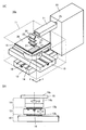
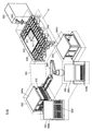
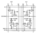
- FIG. 1A is a perspective view illustrating a laser processing apparatus of one embodiment of the present invention.
- the laser processing apparatus 10 a includes a moving mechanism 12, a moving mechanism 13, a rotating mechanism 14, and a fixing mechanism 15 for configuring an xy- ⁇ stage in the chamber 11. Further, it has a laser oscillator 20 for shaping a linear beam, an optical system unit 21, a mirror 22, and a lens 23.
- FIG. 1B is a view of the xy- ⁇ stage as viewed from the lateral direction.
- the moving mechanism 12 has a first movable portion 12b
- the moving mechanism 13 has a second movable portion 13b.
- the first movable part 12b and the second movable part 13b can reciprocate linearly in the horizontal direction.
- a mechanism for supplying power to the first movable portion 12b and the second movable portion 13b for example, a ball screw mechanism 16 driven by a motor can be used.
- the moving mechanism 13 is fixed to the first movable part 12b. Therefore, the moving mechanism 13 can reciprocate linearly in the first horizontal direction (x direction).
- the moving direction of the 1st movable part 12b and the moving direction of the 2nd movable part 13b are installed so that it may orthogonally cross in a horizontal direction. Therefore, by fixing the rotation mechanism 14 to the second movable portion 13b, the rotation mechanism 14 can move in the second direction (y direction) orthogonal to the first direction and the first direction.
- the rotation mechanism 14 includes a third movable portion 14b having a central axis of rotation in the vertical direction.
- a fixing mechanism 15 is fixed to the third movable portion 14b. Therefore, the fixing mechanism 15 can move in the rotational direction ( ⁇ direction) in addition to the first direction (x direction) and the second direction (y direction) described above.
- the fixing mechanism 15 includes a stage 15b having a plane on which the workpiece 30 is fixed.
- the workpiece 30 can be fixed on the stage 15 b by a vacuum suction mechanism or the like provided in the fixing mechanism 15.
- the fixing mechanism 15 may have a heating mechanism as needed.
- the center axis of the third movable portion 14b and the center of the plane of the stage 15b are fixed so as to overlap.
- the stage 15b has a first side and a second side that have a rectangular upper surface and are orthogonal to each other.
- the first side is the long side and the second side is the short side.
- the fixing mechanism 15 includes a pusher pin and its up-and-down mechanism, and the workpiece 30 can be moved up and down when the workpiece 30 is carried into and out of the chamber 11.
- the laser oscillator 20 only needs to be able to output light having a wavelength and intensity suitable for the purpose of processing, and is preferably a pulse laser but may be a CW laser.
- a pulse laser that can emit ultraviolet light with a wavelength of 351 to 353 nm (XeF), 308 nm (XeCl), or the like can be used.
- XeF 351 to 353 nm
- XeCl 308 nm
- a double wave (515 nm, 532 nm, etc.) or a triple wave (343 nm, 355 nm, etc.) of a solid laser (YAG laser, fiber laser, etc.) may be used.
- a plurality of laser oscillators 20 may be provided.
- the optical system unit 21 includes, for example, a mirror, a beam expander, a beam homogenizer, and the like, and extends the in-plane distribution of the energy of the laser light 25 output from the laser oscillator 20 while making it uniform.
- the laser beam 26 output from the optical system unit 21 is preferably formed in a rectangular shape so that the beam shape on the processing surface of the workpiece is linear.
- a dielectric multilayer mirror can be used, and the mirror 22 is installed so that the incident angle of the laser beam is about 45 °.
- a cylindrical lens can be used as the lens 23.
- a quartz window 24 is provided on the upper portion of the chamber 11.
- the entire element other than the laser oscillator 20 may be provided in the chamber 11.
- the quartz window 24 may be provided in a region where the laser beam 25 enters the chamber.
- the quartz window 24 can be replaced with a glass window on the premise that the energy density required for the linear beam 27 is obtained. Further, when the chamber 11 is not provided, the quartz window 24 is unnecessary.
- the laser beam 25 output from the laser oscillator 20 enters the optical system unit 21.
- the laser beam 26 expanded into a rectangular shape by the optical system unit 21 enters the mirror 22.
- the laser beam 26 may be divided into a plurality of parts.
- the laser light 26 emitted from the optical system unit 21 is illustrated as parallel light, but may be light having a spread in the emission direction.
- the length of the linear beam 27 is ideally not less than the length of one side of the workpiece 30.
- the entire workpiece 30 can be laser machined simply by moving the linear beam 27 or the workpiece 30 in one horizontal direction.
- a very expensive large optical component is required.
- the length of the linear beam 27 can be set to about 1 ⁇ 4 of the length of one side of the workpiece 30.
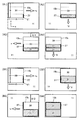
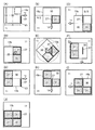
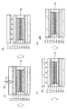
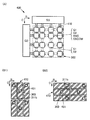
- FIGS. 2A1 to 2A4 and FIGS. 2B1 to 4B4 are conventional examples, and a method of irradiating a workpiece 30 with a linear beam 27 and forming a processing region 31 on the entire surface (effective region). It is a figure explaining.
- a linear beam 27 indicates an irradiation position and is fixed near the center of the chamber 11.
- the workpiece 30 can be moved by a moving mechanism in the xy directions.
- the linear beam 27 can be applied only to a desired region of the workpiece 30 in accordance with the purpose.
- the entire surface of the workpiece 30 can be irradiated. That is, the processing region 31 may be formed with an interval, or the linear beam 27 may be irradiated so as to overlap a part of the processing region 31.
- the description will be made assuming that the size of the stage 15b to which the workpiece 30 is fixed and the size of the workpiece 30 are the same.
- the size of the workpiece 30 may be smaller than the stage 15b.
- 2A1 to 2A4 are examples in which the linear beam 27 is about 1 ⁇ 4 of the length of one side of the stage 15b (workpiece 30).
- the stage 15b is moved in the + x direction while irradiating the linear beam 27 (see FIG. 2 (A1)).
- the stage 15b is moved in the ⁇ y direction (see FIG. 2 (A2)).
- FIGS. 2B1 to 2B4 are examples in which the linear beam 27 is about 1 ⁇ 2 of the length of one side of the stage 15b.
- the basic operation is the same as that described in FIGS. 2A1 to 2A4.
- the ⁇ y direction is used. Is moved once, and the distance is 1 ⁇ 2 of the distance B (see FIG. 2 (B3)).
- the moving range of the first movable portion 12b is the length of the first side of the stage 15b regardless of the linear beam length.
- the stage 15b is moved in the xy direction to irradiate the entire surface of the workpiece 30 with the linear beam 27, so that the occupation area of the chamber 11 needs to be relatively large. is there.
- the inner dimension of the floor of the chamber 11 is about 7/4 times the short side of the second side and about twice the long side of the first side
- the area of the floor of the chamber 11 is about 3.8 times the area of the stage 15b.
- the inner dimension of the floor of the chamber 11 is about 3/2 times the short side of the second side and about twice the long side of the first side.
- the floor area of the chamber 11 is about 3.2 times the area of the stage 15b.
- the moving direction of the stage 15b is not limited to the conventional xy direction, but can also be the rotational direction ( ⁇ direction), and the processing distance of one degree is about 1 ⁇ 2 of one side of the stage 15b. As a result, the area occupied by the chamber 11 is reduced.
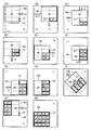
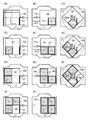
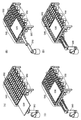
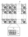
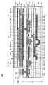
- 3A to 3K are diagrams illustrating the operation of the laser processing apparatus 10a of one embodiment of the present invention illustrated in FIG. 3A to 3K show an example in which the linear beam 27 is about 1 ⁇ 4 of the length of one side of the stage 15b.
- 3A to 3K show a method of irradiating one half surface of the workpiece 30 with laser, rotating the workpiece 30 by 180 °, and irradiating the other half surface of the workpiece 30 with laser. .
- the vicinity of the first vertex V1 of the stage 15b is used as a processing start point, and the stage 15b is moved in the + x direction while irradiating the linear beam 27 (see FIG. 3A).
- the stage 15b is moved in the ⁇ y direction (see FIG. 3B).
- the stage 15b is moved in the ⁇ y direction (see FIG. 3D).
- the stage 15b is moved in the ⁇ y direction (see FIG. 3F).
- the stage 15b is moved to the center of the chamber 11 (see FIG. 3H).
- the stage 15b is rotated 180 °, and the stage 15b is moved to the same position as in FIG. 3A (see FIGS. 3H and I). Thereafter, the vicinity of the third vertex V3 of the stage 15b is used as a processing start point, and the same operation as in FIGS. 3A to 3H is repeated to irradiate the entire surface of the workpiece 30 with the linear beam 27 (FIG. 3 (J) and (K)).
- the moving range of the first movable part 12b is 1 ⁇ 2 of the length of the first side, and the second movable part 13b.
- the entire moving range of the workpiece 30 can be laser-processed by setting the moving range to a length shorter by 1 ⁇ 4 than the length of the second side. That is, when the linear beam length is 1 / X of the second side of the stage 15b, the moving range of the second movable portion 13b may be shorter by 1 / X than the length of the second side.
- the moving range of the first movable part 12b and the moving range of the second movable part 13b are minimum values, and are 2% or more than the above in consideration of reduction of mechanical load and maintainability.
- the movement range may be expanded within a range of 20% or less, preferably 5% or more and 10% or less.
- the inner dimension of the floor of the chamber 11 should be at least about 3/2 times the short side of the first side and about 7/4 times the long side of the first side. Can do.
- the floor area in the chamber 11 is about 2.8 times the area of the stage 15b.
- the conventional example is about 3.8 times, and the occupied area can be significantly reduced.
- the laser processing device of one embodiment of the present invention may have a structure illustrated in FIG.
- a laser processing apparatus 10b shown in FIG. 4A has the same components as the laser processing apparatus 10a.
- the moving range of the second movable portion 13b of the moving mechanism 13 can be made smaller than that of the laser processing apparatus 10a. Accordingly, the inner size of the floor of the chamber 11 can be further reduced.
- a variable shading mechanism 17 for controlling the beam length is provided in the optical path of the laser light 26.
- the linear beam 27 is irradiated at a position parallel to the first side of the workpiece 30, and the second side of the workpiece 30 is parallel. It is possible to correspond to the case of irradiating the linear beam 27 at the position.
- FIG. 4B1 is a diagram showing a state in which the shielding plate is slid in the direction of extending the beam length, and the beam length is a.
- FIG. 4B1 is a diagram showing a state in which the shielding plate is slid in the direction of narrowing the beam length, and the beam length is b (a> b).
- 4B1 and 4B2 illustrate an example in which the light shielding mechanism 17 is provided between the optical system unit 21 and the mirror 22 (not shown), the present invention is not limited thereto.
- the light shielding mechanism 17 may be provided in any region between the mirror 22 and the fixing mechanism 15.
- the light shielding mechanism 17. May not be used.
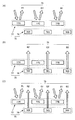
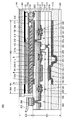
- FIGS. 5A to 5L are diagrams illustrating the operation of the laser processing apparatus 10b according to one embodiment of the present invention illustrated in FIGS. 4A and 4B.
- FIGS. 5A to 5L show an example in which the linear beam 27 is about 1 ⁇ 4 of the length of one side of the stage 15b.
- the first region of the work piece 30 is irradiated with laser, the work piece 30 is rotated by 90 °, and the work piece 30 has a quarter of the first work area.
- This is a method of irradiating the region 2 with laser.
- laser irradiation can be performed on the entire surface of the workpiece 30 by repeating rotation and laser irradiation.
- the stage 15b is moved in the + x direction while irradiating the linear beam 27 (see FIG. 5A).
- the light shielding mechanism 17 is operated so that the length of the linear beam 27 is about 1/4 of the length B of the second side (see FIG. 4 (B2)).
- the stage 15b is moved in the ⁇ y direction (see FIG. 5B).
- the stage 15b is moved to the center of the chamber 11 (see FIG. 5D).
- the stage 15b is rotated by 90 °, and the stage 15b is moved in the ⁇ x + y direction so that the vicinity of the second vertex V2 of the stage 15b becomes the machining start point (see FIGS. 5E and 5F).
- the light shielding mechanism 17 is operated so that the length of the linear beam 27 is about 1 ⁇ 4 of the length A of the first side (see FIG. 4 (B1)).
- the stage 15b is moved in the ⁇ y direction (see FIG. 5G).
- the stage 15b is moved to the center of the chamber 11 (see FIG. 5I).
- the stage 15b is rotated by 90 °, and the stage 15b is moved in the ⁇ x + y direction so that the vicinity of the third vertex of the stage 15b becomes the machining start point (see FIGS. 5J and 5K).
- the light shielding mechanism 17 is operated so that the length of the linear beam 27 is about 1 ⁇ 4 of the length B of the second side (see FIG. 4B2).
- the moving range of the first movable part 12b is 1 ⁇ 2 of the length of the first side, and the second movable part 13b. Is set to 1 ⁇ 4 of the length of the first side, the entire surface of the workpiece 30 can be laser processed. That is, when the linear beam length is 1 / 2X of the first side of the stage 15b (X is an integer of 2 or more), the moving range of the second movable portion 13b is (X + 1) longer than the length of the first side. The length may be shorter by 2X.
- the moving range of the first movable part 12b and the moving range of the second movable part 13b are minimum values, and are 2% or more than the above in consideration of reduction of mechanical load and maintainability.
- the movement range may be expanded within a range of 20% or less, preferably 5% or more and 10% or less.
- the inner dimension of the floor of the chamber 11 can be set so that at least the short axis is approximately the length of the diagonal of the stage 15b and the long side is about 3/2 times the first side. .
- the floor area in the chamber 11 is about 2.3 times the area of the stage 15b.
- the conventional example is about 3.8 times, and the occupied area can be significantly reduced.
- the laser processing device of one embodiment of the present invention may have a configuration illustrated in FIG.
- the laser processing apparatus 10c shown in FIG. 6 has a configuration in which the beam length is about 1 ⁇ 2 of the stage 15b with the laser processing apparatus 10a as a base. Since an operation method different from that of the laser processing apparatus 10a is assumed, the moving range of the second movable portion of the moving mechanism 13 can be made smaller than that of the laser processing apparatus 10a. Accordingly, the inner size of the floor of the chamber 11 can be further reduced.
- FIGS. 7A to 7J are diagrams illustrating the operation of the laser processing apparatus 10c of one embodiment of the present invention illustrated in FIGS. 6A and 6B.
- FIGS. 7A to 7J are examples in the case where the linear beam 27 is about 1 ⁇ 2 of the length of one side of the stage 15b.
- the first region of the quarter of the workpiece 30 is irradiated with laser, the workpiece 30 is rotated by 90 °, and the quarter of the workpiece 30 is obtained.
- This is a method of irradiating the region 2 with laser.
- laser irradiation can be performed on the entire surface of the workpiece 30 by repeating rotation and laser irradiation.
- the vicinity of the first vertex V1 of the stage 15b is used as a processing start point, and the stage 15b is moved in the + x direction while irradiating the linear beam 27 (see FIG. 7A).
- the stage 15b is moved in the ⁇ y direction (see FIG. 7B).
- the stage 15b is moved in the ⁇ x direction (see FIG. 7C).
- the stage 15b is moved to the center of the chamber 11 (see FIG. 7D).
- the stage 15b is rotated by 180 °, and the stage 15b is moved in the ⁇ x + y direction so that the vicinity of the third vertex V3 of the stage 15b becomes the machining start point (see FIGS. 7E and 7F).
- the moving range of the first movable portion 12b is 1 ⁇ 2 of the length of the first side, and the second movable portion 13b.
- the entire moving range of the workpiece 30 can be laser-processed by setting the moving range to a length shorter by 1 ⁇ 2 than the length of the second side. That is, when the linear beam length is 1 / X of the second side of the stage 15b, the moving range of the second movable portion 13b may be shorter by 1 / X than the length of the second side.
- the moving range of the first movable part 12b and the moving range of the second movable part 13b are minimum values, and are 2% or more than the above in consideration of reduction of mechanical load and maintainability.
- the movement range may be expanded within a range of 20% or less, preferably 5% or more and 10% or less.
- the inner dimension of the floor of the chamber 11 should be at least about 3/2 times the short side of the second side and about 3/2 times the long side of the first side. Can do.
- the floor area in the chamber 11 is about 2.4 times the area of the stage 15b.
- the linear beam length is 1 ⁇ 2 of the second side of the stage 15b, it is about 3.2 times, and the occupied area can be greatly reduced.
- the laser processing device of one embodiment of the present invention may have a structure illustrated in FIG.
- the laser processing apparatus 10d shown in FIG. 8A has a configuration in which the laser processing apparatus 10b is a base and the beam length is about 1 ⁇ 2 of the stage 15b. Since an operation method different from that of the laser processing apparatus 10b is assumed, the moving mechanism 13 can be omitted. Accordingly, the inner size of the floor of the chamber 11 can be further reduced. As shown in FIG. 8B, the rotation mechanism 14 is fixed to the first movable portion 12b.
- the light shielding mechanism 17 shown in FIGS. 4B1 and 4B2 is provided in the optical path of the laser light 26.
- FIGS. 9A to 9K are diagrams illustrating the operation of the laser processing apparatus 10d according to one embodiment of the present invention illustrated in FIGS. 8A and 8B.
- FIGS. 9A to 9K show examples in which the linear beam 27 is about 1 ⁇ 2 of the length of one side of the stage 15b.
- the first region of the quarter of the workpiece 30 is irradiated with laser, the workpiece 30 is rotated by 90 °, and the quarter of the workpiece 30 is obtained.
- This is a method of irradiating the region 2 with laser.
- laser irradiation can be performed on the entire surface of the workpiece 30 by repeating rotation and laser irradiation.
- the vicinity of the first vertex V1 of the stage 15b is used as a processing start point, and the stage 15b is moved in the + x direction while irradiating the linear beam 27 (see FIG. 9A).
- the light shielding mechanism 17 is operated so that the length of the linear beam 27 is about 1 ⁇ 2 of the length B of the second side.
- the stage 15b is moved to the center of the chamber 11 (see FIG. 9B).
- the stage 15b is rotated by 90 °, and the stage 15b is moved in the ⁇ x direction so that the vicinity of the second vertex V2 of the stage 15b becomes the machining start point (see FIGS. 9C and 9D).
- the light shielding mechanism 17 is operated so that the length of the linear beam 27 is about 1 ⁇ 2 of the length A of the first side.
- the stage 15b is moved to the center of the chamber 11 (see FIG. 9E).
- the stage 15b is rotated by 90 °, and the stage 15b is moved in the ⁇ x direction so that the vicinity of the third vertex V3 of the stage 15b becomes the machining start point (see FIGS. 9F and 9G).
- the light shielding mechanism 17 is operated so that the length of the linear beam 27 is about 1 ⁇ 2 of the length B of the second side.
- the movement range of the first movable portion 12b is set to 1 ⁇ 2 of the length of the first side, thereby making the entire surface of the stage 15b. Can be laser processed.
- the moving range of the first movable portion 12b is a minimum value, and in consideration of reduction of mechanical load and maintainability, a range of 2% or more and 20% or less than the above, preferably 5% or more.
- the movement range may be expanded within a range of 10% or less.
- the inner dimension of the floor of the chamber 11 can be set so that at least the short axis is approximately the length of the diagonal of the stage 15b and the long side is about 3/2 times the first side. .
- the floor area in the chamber 11 is about 2.1 times the area of the stage 15b.
- the linear beam length is 1 ⁇ 2 of the second side of the stage 15b, it is about 3.2 times, and the occupied area can be greatly reduced.
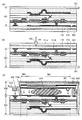
- the workpiece 30 can be a flat substrate 35 and a structure 36 provided on the substrate 35 as shown in FIG.
- the structure 36 can be directly irradiated with the linear beam 27.
- the structure 36 can be, for example, a thin film or a stacked body including the thin film. Specific examples of the thin film include a semiconductor film to be a semiconductor layer of a transistor.
- the substrate 35, the substrate 37, and the layer 38 sandwiched between the two substrates are used.
- At least the substrate 37 on which the laser light is incident is a glass substrate or the like, and is a material that can irradiate the layer 38 with a linear beam 27 having a necessary energy density.
- the layer 38 includes a resin layer such as polyimide, and is a layer that can be processed by being irradiated with a linear beam 27 having a certain intensity or higher.
- the resin layer is provided in contact with the entire surface of the substrate 37. Alternatively, it may be provided so as to partially contact the substrate 37. By laser processing the resin layer, the adhesion between the resin layer and the substrate 37 is lowered, and the layer 38 supported by the substrate 35 and the substrate 37 can be separated.
- the workpiece 30 may have a configuration in which the substrate 35 is removed from the configuration in FIG.
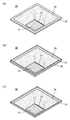
- the layer 38 loses the supported substrate after the workpiece 30 is processed, it is preferable to use an auxiliary jig 40 as shown in FIG.
- the auxiliary jig 40 has a frame 41 and a suction part 42.
- the frame 41 is provided with a notch for mounting the workpiece 30.
- the frame 41 can be formed of, for example, metal or a composite material of metal and ceramic, and the adsorbing portion 42 can be formed of porous ceramics having air permeability.
- FIG. 11A shows an example in which four suction portions 42 are arranged in the notch, but the number of suction portions 42 is not limited.
- FIG. 11B is a cross-sectional view taken along line X1-X2 illustrated in FIG.
- the frame 41 and the suction portion 42 are configured such that no step is generated on either the front or back side.
- FIG. 11C is a diagram illustrating a state where the auxiliary jig 40 on which the workpiece 30 is mounted is fixed to the fixing mechanism 15.
- FIG. 11D is a cross-sectional view taken along line X3-X4 in FIG.
- the fixing mechanism 15 is provided with an opening 43 that communicates with the surface of the stage 15b.
- a vacuum pump or the like By connecting a vacuum pump or the like to the opening 43, a thing in contact with the surface of the stage 15b can be vacuum-sucked.
- the auxiliary jig 40 is installed on the stage 15b so that the opening 43, the suction part 42, and the frame 41 are in contact with each other. By installing the auxiliary jig 40 in this way, the workpiece 30 can be vacuum-adsorbed together with the auxiliary jig via the adsorption portion 42.
- the example in which the mirror 22 is installed so that the incident angle of the laser beam 26 is approximately 45 ° as shown in FIG. 12A is shown, but as shown in FIG.
- the incident angle of the laser beam 26 with respect to the mirror 22 may be an angle smaller than 45 °.
- the angle is 20 ° or more and less than 45 °, preferably 25 ° or more and 40 or less, more preferably 30 ° or more and 40 or less.
- the incident angle of the laser light 26 with respect to the mirror 22 may be an angle larger than 45 °.
- it is greater than 45 ° and 70 ° or less, preferably 50 ° or more and 65 ° or less, more preferably 50 ° or more and 60 ° or less.
- the workpiece 30 can be irradiated with the linear beam 27 obliquely by changing the incident angle of the laser beam 26 with respect to the mirror 22. Therefore, for example, the workpiece 30 has a configuration as shown in FIG. 10B, and when it is desired to irradiate the layer 38 with a linear beam through the substrate 37, processing defects due to foreign matters on the substrate 37 are suppressed. be able to. It is more effective to perform the processing at the above angle.
- the workpiece 30 may be irradiated with a linear beam in any two forms shown in FIGS.
- any one of the forms shown in FIGS. 12A to 12C is selected, the first laser irradiation is performed on the workpiece 30, and the first irradiation is performed on the irradiated region.
- the second laser irradiation may be performed by selecting a form other than the selected form.
- the incident angle of the laser beam 26 with respect to the mirror 22 can be easily changed by changing the angle of the mirror 22.
- a jig 28 provided on the mirror 22 may be rotated by a motor 29.
- a mechanism for moving the workpiece 30 up and down so that the focal point of the linear beam 27 is formed in a desired region may be used.
- the workpiece 30 has a form as shown in FIG. 10B or FIG. 10C and the resin is laser processed, there may be a step of removing the resin in the subsequent steps.
- a laminate processing apparatus in which the laser processing apparatus of one embodiment of the present invention and a plasma processing apparatus (for example, an ashing apparatus) for removing resin are combined.
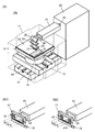
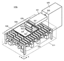
- FIG. 13 is a diagram illustrating an example of the processing apparatus for the laminated body.
- the laminate processing apparatus 10 e includes a set of laser processing apparatuses, a transfer chamber 51, a load / unload chamber 52, an unload chamber 53, and a plasma processing chamber 54.
- each chamber is illustrated in a simplified manner without a gate valve or the like.
- FIG. 13 illustrates the configuration shown in FIG. 1 as a set of laser processing apparatuses
- the configurations shown in FIGS. 4, 6, and 8 may be used.
- the laminated body processing apparatus 10e may have a configuration in which the plasma processing chamber 54 is removed from the configuration shown in FIG. Moreover, it can also be set as the structure remove
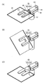
- the transfer chamber 51 includes a transport mechanism 60 and can carry members in and out of the chamber before and after processing.
- the transport mechanism 60 is an arm type robot, and includes an elevating mechanism 61, a joint mechanism 62, arms 63 and 64, a reversing mechanism 65, a fork 66, and the like.
- the workpiece 30 and the like can be transported by the expansion / contraction operation of the arms 63 and 64 around the joint mechanism 62 and the like, the elevating operation of the elevating mechanism 61, and the like.
- the reversing mechanism 65 has a support portion 65a and a rotation portion 65b. As shown in FIG. 14B, the fork 66 can be rotated by the rotation of the rotating portion 65b.
- the suction mechanism 67 is supported on the fork 66 by the suction mechanism 67. Therefore, as shown in FIGS. 14B and 14C, the workpiece 30 and the like can be supported even when the fork 66 is tilted and inverted.
- a vacuum suction mechanism can be used as the suction mechanism 67.
- the suction mechanism 67 may have a suction cup.
- the load / unload chamber 52 has a cassette 45 a and can store the workpiece 30. Further, the processed member 30c carried out from the plasma processing chamber 54 can be stored in the cassette 45a.
- the unload chamber 53 has a cassette 45b and can store the processed member 30a unloaded from the chamber 11 of the laser processing apparatus.
- the member 30a may be stored in the cassette 45a, and the member 30c may be stored in the cassette 45b.
- the plasma processing chamber 54 is provided with a downflow type ashing unit having a plasma generation mechanism 47, a shower plate 48 and a stage 49.
- the plasma generation mechanism 47 is connected to a gas line for supplying oxygen, a rare gas, and the like, a high-frequency power source, and the like, and can generate oxygen radicals. For example, by placing the workpiece 30 with the resin exposed on the surface on the stage 49 and reacting it with oxygen radicals and carbon constituting the resin, the resin can be vaporized and removed.
- the shower plate 48 can suppress the spread of plasma, for example, by using a ground potential. By using the shower plate 48, plasma damage to the workpiece 30 can be suppressed without delaying supply of useful oxygen radicals.
- the stage 49 may be provided with a heater for promoting the reaction.
- the workpiece 30 has the form shown in FIG. 10B and is intended to remove the resin sandwiched between the substrate 35 and the substrate 37 by laser processing and ashing.
- the cassette 45 a storing the workpiece 30 is installed in the load / unload chamber 52, and the workpiece 30 is carried into the chamber 11 of the laser processing apparatus by the transport mechanism 60.
- the member 30a separated from the workpiece 30 (for example, the substrate 37 shown in FIG. 10B) is carried out of the chamber 11 by the transport mechanism 60 and stored in the cassette 45b of the unload chamber 53.
- the member 30 a can be separated from the workpiece 30 by reversing the fork 66 of the transport mechanism 60, sucking the surface of the member 30 a by the suction mechanism 67, and lifting it upward by the lifting mechanism 61.
- the transport mechanism 60 unloads the member 30b from the workpiece 30 and separates the member 30a from the chamber 11 and loads it into the plasma processing chamber 54. Then, the ashing process is started. A multitasking operation for performing laser processing on a new workpiece 30 during the ashing processing may be performed.
- the processed member 30c is unloaded from the plasma processing chamber 54 by the transfer mechanism 60 and stored in the cassette 45a of the load / unload chamber 52.
- laser processing and ashing processing of the workpiece 30 can be continuously performed.
- the processing time can be shortened by performing the multitask operation.
- Embodiment 2 In this embodiment, a laser processing apparatus different from that in Embodiment 1 will be described. Note that the use of the laser processing apparatus is not limited, but it is particularly useful to be used in a manufacturing process of a semiconductor device, a display device, a light emitting device, a power storage device, a power generation device, or the like.
- One embodiment of the present invention is a laser processing apparatus that irradiates a flat plate-shaped workpiece with a laser beam formed into a linear beam.
- the laser processing apparatus can be used for, for example, an application in which a semiconductor layer provided on a supporting substrate is irradiated with laser light to be modified.
- a structure including a resin formed over a supporting substrate can be used for an application in which the resin is processed by irradiating the resin with laser light transmitted through the supporting substrate and the supporting substrate is peeled off.
- the laser processing apparatus includes a laser oscillator and an optical system for forming a linear beam, and a first roller unit and a second roller unit.
- the first roller unit has a function of moving the workpiece in the first horizontal direction (X direction), and the second roller unit moves the workpiece in the second horizontal direction (Y direction) and the vertical direction ( (Z direction).
- the laser irradiation mechanism has a function of irradiating a workpiece to be set on the first roller unit with laser light from below.
- laser irradiation from the support substrate side can be easily performed on the structure formed over the support substrate.
- a conventional laser processing apparatus that irradiates a laser beam from above a workpiece, it is necessary to provide another support substrate or the like on the structure.
- a process of removing the other support substrate is also necessary.
- FIG. 15A is a perspective view illustrating a laser processing device of one embodiment of the present invention.
- the laser processing apparatus 510a has a laser irradiation mechanism for forming a linear beam.
- the chamber 511 includes a first roller unit 540 and a second roller unit 550, and both are disposed so as to have an overlapping region.
- the workpiece 530 is installed on the first roller unit 540.
- FIG. 15B is a diagram illustrating a laser irradiation mechanism.
- the laser irradiation mechanism includes a laser oscillator 520, a mirror 523a, a mirror 523b, a mirror 523c, an optical system unit 521, and a lens 522.
- the laser oscillator 520 only needs to be able to output light having a wavelength and intensity suitable for the purpose of processing, and is preferably a pulse laser but may be a CW laser.
- a pulse laser that can emit ultraviolet light with a wavelength of 351 to 353 nm (XeF), 308 nm (XeCl), or the like can be used.
- XeF 351 to 353 nm
- XeCl 308 nm
- a double wave (515 nm, 532 nm, etc.) or a triple wave (343 nm, 355 nm, etc.) of a solid laser (YAG laser, fiber laser, etc.) may be used.
- a plurality of laser oscillators 520 may be provided.
- the mirror 523a, the mirror 523b, and the mirror 523c for example, a dielectric multilayer mirror can be used, and the mirror 523a, the mirror 523b, and the mirror 523c are installed so that the incident angle of the laser light incident on each of them is about 45 °.
- the optical system unit 521 includes, for example, a mirror, a beam expander, a beam homogenizer, and the like, and expands the in-plane distribution of energy of the laser light 525 output from the laser oscillator 520 while making it uniform.
- the laser beam 526 output from the optical system unit 521 is preferably formed in a rectangular shape so that the beam shape on the processing surface of the workpiece is linear.
- the lens 522 is a condensing lens, and for example, a cylindrical lens can be used.
- the entire element other than the laser oscillator 520 and the mirror 523a is preferably provided in the chamber 511.
- optical components such as a mirror and a lens can be prevented from being deteriorated, and maintenance is facilitated.
- a quartz window 524 is provided in a region where the laser beam 525 enters the chamber 511.
- the quartz window 524 can be replaced with a glass window on the premise that the energy density required for the linear beam 527 can be obtained. In the case where the chamber 511 is not provided, the quartz window 524 is not necessary.
- the laser beam 525 output from the laser oscillator 520 in the horizontal direction is incident on the mirror 523a and reflected downward. Then, the laser beam 525 is reflected by the mirror 523 b and enters the optical system unit 521.
- the laser beam 526 expanded into a rectangular shape by the optical system unit 521 enters the mirror 523c. At this time, the laser beam 526 may be divided into a plurality of parts.
- the laser light 526 emitted from the optical system unit 521 is illustrated as parallel light, but may be light having a spread in the emission direction.
- the laser beam 526 reflected by the mirror 523c enters the lens 522, and forms a linear beam 527 at a desired position on the workpiece 530.
- a desired region of the workpiece 530 can be laser processed by moving the workpiece 530 in the horizontal direction while irradiating the linear beam 527 formed in this manner.
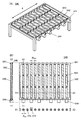
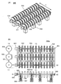
- FIG. 16A is a perspective view illustrating the first roller unit 540.
- FIG. 16B is a top view of the first roller unit 540, a cross-sectional view of X1-X2 and a cross-sectional view of Y1-Y2 shown in the top view.
- the first roller unit 540 includes a plurality of mounts 541, rollers 542, a rotation shaft 543, and a rotation mechanism 544.
- the workpiece 530 is installed on the roller 542.
- the gantry 541 is provided with a rotation mechanism 544.
- One end of the rotation shaft 543 is connected to the rotation mechanism 544, and the other end of the rotation shaft 543 is connected to the gantry 541.
- both ends of the rotation shaft 543 are connected to the mount 541.
- a bearing 546 is provided between the gantry 541 and the rotating shaft 543.
- a cylindrical roller 542 is fixed to the rotation shaft 543. It is preferable that the central axis of the roller 542 has a region overlapping with the central axis of the rotation shaft 543.
- the roller 542 By connecting the rotation mechanism 544 and the rotation shaft 543, the roller 542 can be rotated, and the workpiece 530 on the roller 542 can be moved in the first horizontal direction (X direction).
- 16A and 16B show a configuration in which three rollers 542 are fixed to one rotating shaft 543, but the present invention is not limited to this.
- one long roller 542 may be fixed to the rotation shaft 543.
- the number of rollers may be increased and fixed to the rotating shaft 543 as compared with FIGS. 16A and 16B.
- a roller 542b having a smaller diameter than the roller 542 and a rotating shaft 543b having a smaller diameter than the rotating shaft 543 may be provided. These are not connected to the rotation mechanism 544 but connected to the gantry 541. Thus, by reducing the roller and the rotating shaft, the weight can be reduced, and the resistance of rotation can be reduced. Therefore, the load on the rotation mechanism 544 can be reduced.
- FIGS. 16A and 16B illustrate an example in which there is a set of the rotating shaft 543 and the roller 542 that are not connected to the rotating mechanism 544. However, as illustrated in FIG. In addition, a rotation mechanism 544 may be connected to the set of rollers 542.
- FIG. 17E is a cross-sectional view (Y3-Y4 position) of a part of the top view of the first roller unit 540 and a set of the roller 542 and the rotating shaft 543 that are not connected to the rotating mechanism 544.
- a bearing 546 may be provided between the roller 542 and the rotation shaft 543 in order to reduce rotation resistance.
- control In laser processing, control must be performed so that the position of the workpiece in the height direction does not change so that the energy density of the laser beam does not vary on the irradiated surface.
- the level of the stage and the flatness of the stage surface are important because the stage position and the laser irradiation position always change.
- a large stage with high flatness is required, which increases the manufacturing cost.
- a sensor for maintaining the level of a large stage equipped with a moving mechanism and frequent maintenance are required.
- the structure which mounts a to-be-processed object on the roller which is 1 aspect of this invention is a structure by which the position of a roller and a laser irradiation position do not change.
- a mechanism for moving the large stage is also unnecessary, so there is little vibration, and the tilt of the roller due to changes over time is less likely to occur. Therefore, it can be said that the apparatus has good maintainability.
- the manufacturing cost can be reduced.
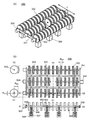
- FIG. 18A is a perspective view illustrating the second roller unit 550.
- FIG. 18B is a top view of the second roller unit 550, a cross-sectional view along X1-X2 and a cross-sectional view along Y1-Y2 shown in the top view.
- the second roller unit 550 includes a plurality of mounts 551, rollers 552, a rotation shaft 553, a rotation mechanism 554, a bearing portion 555, and an elevating mechanism 556.
- the gantry 551 is provided with a rotation mechanism 554. One end of the rotation shaft 553 is connected to the rotation mechanism 554, and the other end of the rotation shaft 553 is connected to the gantry 551.
- a bearing 559 is provided between the gantry 551 and the rotating shaft 553.
- the mount 551 is provided with a plurality of bearing portions 555 that support the rotating shaft 553.
- a cylindrical roller 552 is fixed to the rotation shaft 553.
- the central axis of the roller 552 preferably has a region overlapping with the central axis of the rotating shaft 553.
- the roller 552 By connecting the rotation mechanism 554 and the rotation shaft 553, the roller 552 can be rotated, and the workpiece 530 can be placed on the roller 552 and moved in the second horizontal direction (Y direction).
- the elevating mechanism 556 has a cylinder portion 557 and a rod portion 558, and can raise and lower the rod portion 558 by controlling power.
- a stand 551 is connected to the rod portion 558. Therefore, by operating the lifting mechanism 556, the gantry 551, the roller 552, and the like can be lifted and lowered.
- 18A and 18B show a form in which the rod portion 558 and the bearing portion 555 are connected to each other, the rod portion 558 may be connected to any part of the gantry 551. That's fine.
- the central portion of the second roller unit 550 serves as an optical path for laser light, and thus the roller 552 and the rotation shaft 553 are not disposed. Therefore, in the center row in FIG. 18B, one set of the roller 552, the rotation shaft 553, and the rotation mechanism 554 is provided on the left and right.
- 18A and 18B show an example in which the set of the roller 552, the rotation shaft 553, and the rotation mechanism 554 is arranged in three rows. In order to move the workpiece 530, at least It suffices if the set has two or more rows.
- the roller 552 moves up and down in a region where the roller 542 is not provided in the first roller unit 540. Therefore, the width 552 (corresponding to the height of the cylinder) of the roller 552 can be raised and lowered by making it smaller than the distance W 542 between the adjacent rollers 542 (see FIG. 16B).
- the roller 552 is raised to a desired height by making the radius R 553 of the roller 552 larger than 2R 542 + R 553. Can be made.
- the rotating shaft 553 and the roller 542 may collide when the roller 552 is lifted.
- roller 542 and the roller 552 for example, a cylinder made of metal or resin, a cylinder made of an elastic body such as rubber, or a surface provided with an elastic body made of rubber or the like on the surface of a cylinder made of metal or resin can be used.
- the resin and the elastic body preferably have conductivity in order to prevent deterioration of the device included in the workpiece 530 due to charging.
- a motor can be used.
- a motor with high positional accuracy such as a stepping motor is preferable.
- a sensor for detecting the position of the workpiece 530 may be provided in order to prevent displacement due to the influence of backlash.
- an electric cylinder using a ball screw or the like, a hydraulic cylinder, an air cylinder, or the like can be used as the lifting mechanism 556.
- first roller unit 540 and the second roller unit 550 are not limited, and an appropriate number may be selected in accordance with the size and weight of the workpiece 530.
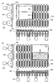
- 19A, 19B, 20A, and 20B illustrate a method of irradiating a workpiece 530 with a linear beam 527 and forming a processed region 531 on the entire surface (effective region). It is a top view, a front view, and a side view. For the sake of clarity, the frame 541 and the rotation mechanism 544 of the first roller unit 540 and the frame 551 and the rotation mechanism 554 of the second roller unit 550 are omitted.
- a linear beam 527 indicates an irradiation position and is fixed near the center of the chamber 511.
- the length of the linear beam 527 is equal to or longer than the length of one side of the workpiece 530.
- the entire workpiece 530 can be laser machined simply by moving the linear beam 527 or the workpiece 530 in one horizontal direction.
- a very expensive large optical component is required.
- the linear beam 527 can irradiate only a desired region of the workpiece 530 in accordance with the purpose.
- the entire surface of the workpiece 530 can be irradiated. That is, the processing region 531 may be formed with an interval, or the linear beam 527 may be irradiated so as to overlap with a part of the processing region 531.
- the workpiece 530 is installed at a predetermined position on the roller 542.
- the lifting mechanism 556 of the second roller unit 550 is lowered, and at least the top of the roller 552 is positioned lower than the top of the roller 542.
- the roller 542 is rotated while irradiating the linear beam 527, and the workpiece 530 is moved in the + X direction (see FIG. 19A). ).
- the irradiation of the linear beam 527 is finished. Then, using the lifting mechanism 556, at least the top of the roller 552 is set to be higher than the top of the roller 542, and the workpiece 530 is lifted. Then, the roller 552 is rotated to move the workpiece 530 in the ⁇ Y direction (see FIG. 19B).
- the top of the roller 552 is positioned lower than the top of the roller 542 using the lifting mechanism 556.
- the workpiece 530 is placed on the roller 542. Then, the irradiation of the linear beam 527 is started, the roller 542 is rotated, and the workpiece 530 is moved in the ⁇ X direction (see FIG. 20A).
- the length of the linear beam 527 is about 1 ⁇ 2 of the length of one side of the workpiece 530, but the length of the linear beam 527 is even shorter.
- the basic operation is the same.
- the length of the linear beam 527 is about ⁇ of the length of one side of the workpiece 530, the number of movements in the ⁇ Y direction is two, and the number of times of laser irradiation is three.
- the length of the linear beam 527 is about 1 ⁇ 4 of the length of one side of the workpiece 530, the number of movements in the ⁇ Y direction is three and the number of laser irradiations is four.
- the shorter the linear beam length the longer the moving distance in the Y direction, and thus the size of the chamber 511 needs to be increased.
- the workpiece 530 can be a flat substrate 535 and a layer 538 provided over the substrate 535 as shown in FIG.
- the layer 538 can be irradiated with a linear beam 527 through the substrate 535.
- the substrate 535 is a glass substrate that has a relatively high transmittance of laser light, and is a material that can irradiate the layer 538 with a linear beam 527 having a necessary energy density.
- the layer 538 includes, for example, a resin layer such as polyimide, and the resin layer can be processed by being irradiated with a linear beam 527 having a certain intensity or higher.
- the resin layer is provided so as to be in contact with the entire surface of the substrate 535. Alternatively, it may be provided so as to be in partial contact with the substrate 535. By laser processing the resin layer, the adhesion between the resin layer and the substrate 535 is reduced, and the layer 538 and the substrate 535 can be separated.
- the workpiece 530 can include a substrate 535, a substrate 537, and a layer 538 sandwiched between the two substrates.
- the incident angle of the laser beam 526 with respect to the mirror 523c may be an angle smaller than 45 °.
- the angle is 20 ° or more and less than 45 °, preferably 25 ° or more and 40 or less, more preferably 30 ° or more and 40 or less.
- the incident angle of the laser beam 526 with respect to the mirror 523c may be an angle larger than 45 °.
- it is greater than 45 ° and 70 ° or less, preferably 50 ° or more and 65 ° or less, more preferably 50 ° or more and 60 ° or less.
- the linear beam 527 can be irradiated obliquely to the workpiece 530 by changing the incident angle of the laser beam 526 with respect to the mirror 523c. Therefore, for example, the workpiece 530 is configured as shown in FIGS. 20A and 20B, and when it is desired to irradiate the layer 538 with a linear beam through the substrate 535, the workpiece 530 is not affected by the foreign matter attached to the substrate 535. The resulting processing failure can be suppressed. It is more effective to perform the processing at the above angle.
- the workpiece 530 may be irradiated with a linear beam in any two forms shown in FIGS.
- the first laser irradiation is performed on the workpiece 530 by selecting any one of the forms shown in FIGS. 22A to 22C, and the first irradiation is performed on the irradiated region.
- the second laser irradiation may be performed by selecting a form other than the selected form.
- the incident angle of the laser beam 526 with respect to the mirror 523c can be easily changed by changing the angle of the mirror 523c.
- a jig 528 provided on the mirror 523c may be rotated by a motor 529.
- a mechanism for raising and lowering the mirror 523c to the lens 522 of the laser irradiation mechanism may be used so that the focal point of the linear beam 527 is formed in a desired region.
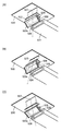
- FIG. 23 shows an example of a configuration in which a carry-in / out device for the workpiece 530 is added to the laser processing device described above.
- a processing apparatus 510b illustrated in FIG. 23 includes a set of laser processing apparatuses, a transfer chamber 561, load chambers 562 and 563, and unload chambers 564 and 565.
- each chamber is illustrated in a simplified manner without a gate valve or the like.
- the structure provided with two load chambers and two unload chambers is shown, the structure provided with one each may be sufficient. Or the structure which serves as a load chamber and an unload chamber in one chamber
- the transfer chamber 561 includes a transport mechanism 560 and can carry members in and out of the chambers before and after processing.
- the transport mechanism 560 is an arm type robot and includes an elevating mechanism, a joint mechanism, an arm, a fork, and the like.
- the workpiece 530 and the like can be transported by an arm extending / contracting operation with a joint mechanism or the like as an axis, or an elevating operation of the elevating mechanism.
- the workpiece 530 is supported on the fork by an adsorption mechanism.
- a vacuum suction mechanism can be used as the suction mechanism.
- the suction mechanism may have a suction cup.
- the load chambers 562 and 563 have cassettes 566a and 566b, and can store an unprocessed workpiece 530.
- the unload chambers 564 and 565 have cassettes 566c and 566d, and can store the processed member 530a unloaded from the chamber 511 of the laser processing apparatus.
- the workpiece 530 has a configuration illustrated in FIG. 21A and is intended for laser processing of a resin provided over the substrate 535.
- the cassette 566a storing the workpiece 530 is installed in the load chamber 562, and the workpiece 530 is carried into the chamber 511 of the laser processing apparatus by the transport mechanism 560.
- the fork of the transport mechanism 560 is inserted into the load chamber 562, and the workpiece 530 is taken out from the cassette 566a.
- the roller 552 of the second roller unit 550 is lowered (see FIG. 24A).
- the workpiece 530 on the fork of the transport mechanism 560 is transported to the prescribed X and Y positions on the first roller unit 540 and the second roller unit 550 in the chamber 511. Then, the roller 552 is lifted by the lifting mechanism 556 to lift the workpiece 530 from the fork of the transport mechanism 560 (see FIG. 24B).
- the fork of the transport mechanism 560 is moved to the outside of the chamber 511 (see FIG. 24C).
- the roller 552 is lowered by the lifting mechanism 556, and the workpiece 530 is installed on the roller 542.
- the roller 552 may be rotated and the roller 552 may be lowered after the workpiece 530 is moved to a desired Y position.
- the workpiece 530 can be transferred into the chamber 511 (see FIG. 24D).
- the workpiece 530 installed on the roller 542 moves to the desired X and Y positions where laser processing is started using the roller 542 or the roller 552.
- the workpiece 530 is laser processed by the method described with reference to FIGS. 19 and 20 to form a processed member 530a. Then, using the roller 542 or the roller 552, the member 530a is moved to the prescribed X and Y positions.
- the roller 552 is raised to lift the member 530a from the roller 542, and the fork of the transport mechanism 560 is inserted between the roller 542 and the member 530a. Then, the roller 552 is lowered to place the member 530a on the fork.
- the member 530a placed on the fork of the transport mechanism 560 is moved to the outside of the chamber 511, and the member 530a is stored in the cassette 566c installed in the unload chamber 564.
- the workpiece 530 can be carried in and the member 530a can be carried out using the roller for moving the workpiece 530 and the like. Since the loading / unloading method does not use a lift pin or the like, the apparatus can be manufactured at low cost.
- first roller unit 540 and the second roller unit 550 can be applied to a configuration in which laser light is irradiated from above the workpiece 530 as shown in FIG.
- a laser processing apparatus 510c shown in FIG. 25 is different from the laser processing apparatus 510a shown in FIGS. 15A and 15B except for a part of the configuration of the laser irradiation mechanism and a part of the configuration of the second roller unit 550. It is the same composition.
- the optical system unit 521 to the lens 522 can be disposed above the first roller unit 540 and the second roller unit 550, so that the mirror 523a and the mirror 523b shown in FIG. be able to.
- a roller 552 at the center of the second roller unit 550 can be installed. Accordingly, since all the rollers 552 in the central row can be fixed to one rotation shaft 553, the set of the roller 552, the rotation shaft 553, and the rotation mechanism 554 becomes one in the center row in FIG. .
- the structure of the laser processing apparatus is described as one embodiment of the present invention.
- the configuration in which the first roller unit 540 and the second roller unit 550 included in the laser processing apparatus are combined can be used not only for laser processing but also for other applications.
- a resin layer is formed over a substrate, a transistor including an oxide semiconductor is formed in a channel formation region over the resin layer, and the resin layer is irradiated with laser light formed into a linear beam. This is a peeling method for separating a transistor and a substrate.
- a metal oxide is used for a channel formation region of the transistor.
- LTPS Low Temperature Poly-Silicon
- the maximum temperature of the process reaches about 500 ° C. to about 550 ° C., and thus heat resistance is required for the resin layer.
- the resin layer needs to be thickened to alleviate damage to the surrounding insulating layer and the like in the laser crystallization process.
- a transistor using a metal oxide does not require heat treatment at high temperature and can be formed at 350 ° C. or lower, further 300 ° C. or lower. Therefore, high heat resistance is not required for the resin layer. Therefore, a relatively inexpensive resin having a low heat-resistant temperature can be used for the resin layer.
- a transistor using a metal oxide does not require a laser crystallization process.
- the band gap of the metal oxide is as wide as 2.5 eV or more and 3.5 eV or less, and the absorption of laser light having a specific wavelength is less than that of silicon, so there is no problem even if the thickness of the resin layer is reduced. Since the resin layer does not require high heat resistance and can be made thin, it can be expected to greatly reduce the cost of device fabrication. Further, the process can be simplified as compared with the case of using LTPS.
- a transistor or the like is formed at a temperature equal to or lower than the heat resistant temperature of the resin layer.
- the heat resistance of the resin layer can be evaluated by, for example, a weight reduction rate by heating, specifically, a 5% weight reduction temperature.
- the 5% weight loss temperature of the resin layer is preferably 450 ° C. or less, more preferably 400 ° C. or less, and further preferably less than 350 ° C.
- the transistor is manufactured at a temperature of 350 ° C. or lower, further 300 ° C. or lower.
- the resin layer may be formed using a photosensitive material.
- a resin layer having a desired shape can be easily formed.
- a resin layer having an opening or a resin layer having two or more regions each having a different thickness can be easily formed. Thereby, it can prevent that a resin layer becomes obstructive preparation of a back gate, an external connection terminal, a penetration electrode, etc.
- a flexible display device can be manufactured using the structure peeling method of one embodiment of the present invention.
- An example of a method for manufacturing a flexible display device is described with reference to FIGS.
- a stacked body 130 in which the stacked body 110 and the stacked body 120 are bonded together with an adhesive layer 132 is obtained.
- the stacked body 110 includes, for example, a substrate 111, a release layer 171, a resin layer 112, an insulating layer 113, a first element layer 114, and a second element layer 131.
- the stacked body 120 includes, for example, a substrate 121, a release layer 172, a resin layer 122, an insulating layer 123, and a functional layer 124.
- the stacked body 130 corresponds to the workpiece 30 described in FIG. 10B of the first embodiment.
- the substrate 111 corresponds to the substrate 35
- the substrate 121 corresponds to the substrate 37.
- the peeling layer 171, the resin layer 112, the insulating layer 113, the first element layer 114, the second element layer 131, the functional layer 124, the insulating layer 123, the resin layer 122, and the peeling layer 172 correspond to the layer 38. .
- the substrates 111 and 121 a hard substrate can be used, and for example, a glass substrate or the like can be used. Since the resin layers 112 and 122 are irradiated with laser light through the substrates 111 and 121 in a later step, the substrates 111 and 121 preferably have high transmittance of the laser light.
- a metal or a metal oxide can be used as the peeling layers 171 and 172.
- various metals such as titanium, molybdenum, aluminum, tungsten, and tantalum, or alloys can be used as the metal.
- metal oxide oxides of various metals can be used.
- titanium oxide, molybdenum oxide, aluminum oxide, tungsten oxide, indium tin oxide, indium zinc oxide, In—Ga—Zn oxide, and the like can be given.
- the resin layers 112 and 122 for example, a material having photosensitivity and thermosetting can be used. Specifically, it is preferable to use a resin such as polyimide. By changing the adhesion between the release layers 171 and 172 and the resin layers 112 and 122, a structure capable of being peeled can be obtained.
- an inorganic insulating layer can be used as the insulating layers 113 and 123.
- the first element layer 114 can include a transistor including an oxide semiconductor in a channel formation region, for example.
- the second element layer 131 can include, for example, an EL element.
- the functional layer 124 can include at least one of a coloring layer such as a color filter, a light shielding layer such as a black matrix, and a detection element such as a touch sensor, for example.
- a coloring layer such as a color filter
- a light shielding layer such as a black matrix
- a detection element such as a touch sensor
- laser light 160 is irradiated from the substrate 121 side onto a processing region (a region including the separation layer 172 and the resin layer 122). Due to the structure change caused by heating the peeling layer 172, the resin layer 122, and the interface thereof by irradiation with the laser light 160, the adhesion between them can be reduced. Irradiation with the laser light 160 is preferably performed with a linear beam, and the laser processing apparatus of one embodiment of the present invention can be used.
- the laser beam is irradiated to the processing region through the substrate 121, if there is a foreign substance on the surface of the substrate 121, the laser beam irradiated to the processing region is blocked, and a separation defect in a subsequent process is locally generated.
- a metal or metal oxide used as the peeling layer 172 adhesion between the peeling layer 172 and the resin layer 122 can be reduced in a range wider than a region irradiated with the laser light. Therefore, even if the laser beam is blocked on the surface of the substrate 121 by a foreign substance or the like, it is possible to suppress a peeling defect in a subsequent process.
- the stack of the substrate 121 and the separation layer 172 is separated from the stack 130 by a physical means.
- the peeling can be performed by fixing the substrate 111 with a suction stage or the like and applying a physical force that moves the substrate 121 side upward.
- the exposed resin layer 122 and the substrate 151 are attached to each other.
- the substrate 151 preferably has flexibility.
- the resin layer 122 and the substrate 151 can be bonded using an adhesive.
- laser light 160 is irradiated from the substrate 111 side onto a processing region (a region including the separation layer 171 and the resin layer 112).
- the stack of the substrate 111 and the separation layer 171 is separated from the stack illustrated in FIG. 28A by physical means.
- the substrate 141 preferably has flexibility.
- the flexible display device 100 illustrated in FIG. 28D can be manufactured.
- Hybrid display is a method of displaying characters or images on one panel by using reflected light and self-light emission in combination with each other to complement color tone or light intensity.
- the hybrid display is a method for displaying characters and / or images using light from a plurality of display elements in the same pixel or the same sub-pixel.
- the display is performed using a pixel or sub-pixel displayed using any one of a plurality of display elements and two or more of the plurality of display elements. A pixel or a sub-pixel.
- a display that satisfies any one or a plurality of expressions of the above configuration is referred to as a hybrid display.
- the hybrid display has a plurality of display elements in the same pixel or the same sub-pixel.
- the plurality of display elements include a reflective element that reflects light and a self-luminous element that emits light. Note that the reflective element and the self-luminous element can be controlled independently.
- the hybrid display has a function of displaying characters and / or images using either one or both of reflected light and self-light emission in the display unit.
- the display device of one embodiment of the present invention can include a pixel provided with a first display element that reflects visible light.
- a pixel provided with a second display element that emits visible light can be provided.
- the pixel can include a pixel provided with a first display element and a second display element.
- a display device including a first display element that reflects visible light and a second display element that emits visible light will be described.
- the display device has a function of displaying an image with one or both of first light reflected by the first display element and second light emitted by the second display element.
- the display device functions to express gradation by controlling the amount of first light reflected by the first display element and the amount of second light emitted by the second display element, respectively.
- the display device controls the first pixel that expresses gradation by controlling the amount of reflected light from the first display element, and the gradation by controlling the amount of light emitted from the second display element.
- a structure including the second pixel to be expressed is preferable.
- a plurality of first pixels and second pixels are arranged in a matrix, for example, and constitute a display unit.
- the first pixels and the second pixels are arranged in the display area with the same number and the same pitch.
- the adjacent first pixel and second pixel can be collectively referred to as a pixel unit.
- the first display element included in the first pixel an element that reflects external light for display can be used. Since such an element does not have a light source, power consumption during display can be extremely reduced.
- a reflective liquid crystal element can be typically used.
- a first display element in addition to a shutter type MEMS (Micro Electro Mechanical System) element, an optical interference type MEMS element, a microcapsule type, an electrophoretic type, an electrowetting type, an electronic powder fluid (registered trademark) An element to which a method or the like is applied can be used.
- a shutter type MEMS Micro Electro Mechanical System
- an optical interference type MEMS element in addition to a shutter type MEMS (Micro Electro Mechanical System) element, an optical interference type MEMS element, a microcapsule type, an electrophoretic type, an electrowetting type, an electronic powder fluid (registered trademark)
- An element to which a method or the like is applied can be used.
- the second display element included in the second pixel includes a light source, and an element that performs display using light from the light source can be used.
- an electroluminescent element that can extract light emitted from a light-emitting substance by applying an electric field is preferably used.
- the light emitted from such a pixel is not affected by the brightness or chromaticity of the light, and therefore has high color reproducibility (wide color gamut) and high contrast, that is, vivid display. be able to.
- a self-luminous light-emitting element such as an OLED (Organic Light Emitting Diode), an LED (Light Emitting Diode), a QLED (Quantum-Dot Light Emitting Diode), or a semiconductor laser can be used.
- a self-luminous light-emitting element such as an OLED (Organic Light Emitting Diode), an LED (Light Emitting Diode), a QLED (Quantum-Dot Light Emitting Diode), or a semiconductor laser
- a combination of a backlight that is a light source and a transmissive liquid crystal element that controls the amount of light transmitted through the backlight may be used.
- the first pixel can include a sub-pixel that exhibits, for example, white (W), or a sub-pixel that exhibits three colors of light, for example, red (R), green (G), and blue (B). .
- the second pixel has a sub-pixel that exhibits, for example, white (W), or a sub-pixel that exhibits light of three colors, for example, red (R), green (G), and blue (B). can do.
- the subpixels included in each of the first pixel and the second pixel may have four or more colors. As the number of subpixels increases, power consumption can be reduced and color reproducibility can be improved.
- a first mode in which an image is displayed with a first pixel a second mode in which an image is displayed with a second pixel, and an image is displayed with the first pixel and the second pixel.
- the third mode can be switched. Further, as shown in Embodiment Mode 1, a different image signal can be input to each of the first pixel and the second pixel to display a composite image.
- the first mode is a mode in which an image is displayed using reflected light from the first display element.
- the first mode is a driving mode with extremely low power consumption because no light source is required. For example, it is effective when the illuminance of outside light is sufficiently high and the outside light is white light or light in the vicinity thereof.
- the first mode is a display mode suitable for displaying character information such as books and documents.
- the reflected light since the reflected light is used, it is possible to perform display that is kind to the eyes, and the effect that the eyes are less tired is achieved.
- the second mode an image is displayed using light emitted from the second display element. Therefore, an extremely vivid display (high contrast and high color reproducibility) can be performed regardless of the illuminance and chromaticity of external light. For example, it is effective when the illuminance of outside light is extremely small, such as at night or in a dark room. Further, when the outside light is dark, the user may feel dazzled when performing bright display. In order to prevent this, it is preferable to perform display with reduced luminance in the second mode. Thereby, in addition to suppressing glare, power consumption can also be reduced.
- the second mode is a mode suitable for displaying a vivid image or a smooth moving image.
- display is performed using both reflected light from the first display element and light emission from the second display element.
- driving is performed so as to express one color by mixing light emitted by the first pixel and light emitted by the second pixel adjacent to the first pixel. While displaying more vividly than in the first mode, it is possible to suppress power consumption as compared with the second mode. For example, it is effective when the illuminance of outside light is relatively low, such as under room lighting or in the morning or evening hours, or when the chromaticity of outside light is not white.
- FIG. 29 illustrates a pixel array 70 included in the display device of one embodiment of the present invention.
- the pixel array 70 has a plurality of pixel units 75 arranged in a matrix.
- the pixel unit 75 includes a pixel 76 and a pixel 77.
- FIG. 29 illustrates an example in which the pixel 76 and the pixel 77 have display elements corresponding to three colors of red (R), green (G), and blue (B), respectively.
- the pixel 76 includes a display element 76R corresponding to red (R), a display element 76G corresponding to green (G), and a display element 76B corresponding to blue (B).
- the display elements 76R, 76G, and 76B are second display elements that use light from the light source.
- the pixel 77 includes a display element 77R corresponding to red (R), a display element 77G corresponding to green (G), and a display element 77B corresponding to blue (B).
- the display elements 77R, 77G, and 77B are first display elements that utilize reflection of external light.
- FIGS. 30A, 30 ⁇ / b> B, and 30 ⁇ / b> C are schematic diagrams illustrating a configuration example of the pixel unit 75.
- the pixel 76 includes a display element 76R, a display element 76G, and a display element 76B.
- the display element 76 ⁇ / b> R has a light source and emits red light R ⁇ b> 2 having luminance corresponding to the gradation value corresponding to red included in the second gradation value input to the pixel 76 to the display surface side.
- the display element 76G and the display element 76B each emit green light G2 or blue light B2 to the display surface side.
- the pixel 77 includes a display element 77R, a display element 77G, and a display element 77B.
- the display element 77R reflects external light and emits red light R1 having a luminance corresponding to the gradation value corresponding to red included in the first gradation value input to the pixel 77 to the display surface side.
- the display element 77G and the display element 77B respectively emit green light G1 or blue light B1 to the display surface side.
- FIG. 30A illustrates an example of an operation mode in which an image is displayed by driving the display element 77R, the display element 77G, and the display element 77B that reflect external light.
- the pixel unit 75 does not drive the pixel 76, for example, when the illuminance of outside light is sufficiently high, and does not drive the pixel 76 (light R1, light G1, and light).
- By mixing only B1) it is possible to emit light 79 of a predetermined color to the display surface side. Thereby, driving with extremely low power consumption can be performed.
- FIG. 30B illustrates an example of an operation mode in which the display element 76R, the display element 76G, and the display element 76B are driven to display an image.
- the pixel unit 75 does not drive the pixel 77, for example, when the illuminance of outside light is extremely small, and the light from the pixel 76 (light R2, light G2, and light B2). ) Only, it is possible to emit light 79 of a predetermined color to the display surface side. Thereby, a vivid display can be performed. Further, by reducing the luminance when the illuminance of outside light is small, it is possible to suppress glare that the user feels and to reduce power consumption.
- FIG. 30C illustrates an operation in which an image is displayed by driving both the display element 77R, the display element 77G, and the display element 77B that reflect external light, and the display element 76R, the display element 76G, and the display element 76B that emit light.
- An example of the mode is shown.
- the pixel unit 75 mixes six lights of light R1, light G1, light B1, light R2, light G2, and light B2 to mix light 79 of a predetermined color. It can be emitted to the display surface side.
- the display panel exemplified below is a display panel that includes both a reflective liquid crystal element and a light-emitting element and can perform both transmission mode and reflection mode displays.
- FIG. 31A is a block diagram illustrating an example of a structure of the display device 400.
- the display device 400 includes a plurality of pixels 410 arranged in a matrix on the display portion 362.
- the display device 400 includes a circuit GD and a circuit SD.
- a plurality of pixels 410 arranged in the direction R a plurality of wirings G1 electrically connected to the circuit GD, a plurality of wirings G2, a plurality of wirings ANO, and a plurality of wirings CSCOM are provided.
- a plurality of pixels 410 arranged in the direction C, a plurality of wirings S1 electrically connected to the circuit SD, and a plurality of wirings S2 are provided.
- circuit GD and the circuit SD that drive the liquid crystal element and the circuit GD and the circuit SD that drive the light emitting element are separately provided. May be provided.
- the pixel 410 includes a reflective liquid crystal element and a light-emitting element.
- the liquid crystal element and the light-emitting element have portions that overlap each other.
- FIG. 31B1 illustrates a configuration example of the conductive layer 311b included in the pixel 410.
- the conductive layer 311b functions as a reflective electrode of the liquid crystal element in the pixel 410.
- an opening 451 is provided in the conductive layer 311b.
- the light-emitting element 360 located in a region overlapping with the conductive layer 311b is indicated by a broken line.
- the light-emitting element 360 is disposed so as to overlap with the opening 451 included in the conductive layer 311b. Thereby, the light emitted from the light emitting element 360 is emitted to the display surface side through the opening 451.
- the pixel 410 adjacent in the direction R is a pixel corresponding to a different color.
- the openings 451 are preferably provided at different positions in the conductive layer 311b so as not to be arranged in a line. Accordingly, the two light-emitting elements 360 can be separated from each other, and a phenomenon (also referred to as crosstalk) in which light emitted from the light-emitting elements 360 enters the colored layer of the adjacent pixel 410 can be suppressed.
- the two adjacent light emitting elements 360 can be arranged apart from each other, a display device with high definition can be realized even when the EL layer of the light emitting element 360 is separately formed using a shadow mask or the like.
- the display using the liquid crystal element becomes dark. If the ratio of the total area of the openings 451 to the total area of the non-openings is too small, the display using the light emitting element 360 is darkened.
- the shape of the opening 451 can be, for example, a polygon, a rectangle, an ellipse, a circle, a cross, or the like. Moreover, it is good also as an elongated streak shape, a slit shape, and a checkered shape. Further, the opening 451 may be arranged close to adjacent pixels. Preferably, the opening 451 is arranged close to other pixels displaying the same color. Thereby, crosstalk can be suppressed.
- FIG. 32 is a circuit diagram illustrating a configuration example of the pixel 410. In FIG. 32, two adjacent pixels 410 are shown.
- the pixel 410 includes a switch SW1, a capacitor C1, a liquid crystal element 340, a switch SW2, a transistor M, a capacitor C2, a light emitting element 360, and the like.
- the pixel 410 is electrically connected to a wiring G1, a wiring G2, a wiring ANO, a wiring CSCOM, a wiring S1, and a wiring S2.
- a wiring VCOM1 electrically connected to the liquid crystal element 340 and a wiring VCOM2 electrically connected to the light emitting element 360 are illustrated.
- FIG. 32 shows an example in which transistors are used for the switch SW1 and the switch SW2.
- the switch SW1 has a gate connected to the wiring G1, one source or drain connected to the wiring S1, and the other source or drain connected to one electrode of the capacitor C1 and one electrode of the liquid crystal element 340. Yes.
- the other electrode of the capacitor C1 is connected to the wiring CSCOM.
- the other electrode of the liquid crystal element 340 is connected to the wiring VCOM1.
- the switch SW2 has a gate connected to the wiring G2, one of the source and the drain connected to the wiring S2, and the other of the source and the drain connected to one electrode of the capacitor C2 and the gate of the transistor M. .
- the other electrode of the capacitor C2 is connected to one of the source and the drain of the transistor M and the wiring ANO.
- the transistor M the other of the source and the drain is connected to one electrode of the light emitting element 360.
- the other electrode of the light emitting element 360 is connected to the wiring VCOM2.
- FIG. 32 shows an example in which the transistor M has two gates sandwiching a semiconductor and these are connected. As a result, the current that can be passed by the transistor M can be increased.
- a signal for controlling the switch SW1 to be in a conductive state or a non-conductive state can be supplied to the wiring G1.
- a predetermined potential can be applied to the wiring VCOM1.
- a signal for controlling the alignment state of the liquid crystal included in the liquid crystal element 340 can be supplied to the wiring S1.
- a predetermined potential can be applied to the wiring CSCOM.
- a signal for controlling the switch SW2 to be in a conductive state or a non-conductive state can be supplied to the wiring G2.
- the wiring VCOM2 and the wiring ANO can each be supplied with a potential at which a potential difference generated by the light emitting element 360 emits light.
- a signal for controlling the conduction state of the transistor M can be supplied to the wiring S2.
- the pixel 410 illustrated in FIG. 32 can be driven by a signal supplied to the wiring G1 and the wiring S1 and can display using optical modulation by the liquid crystal element 340.
- display can be performed by driving the light-emitting element 360 to emit light by driving with signals given to the wiring G2 and the wiring S2.
- the driving can be performed by signals given to the wiring G1, the wiring G2, the wiring S1, and the wiring S2.
- FIG. 32 illustrates an example in which one pixel 410 includes one liquid crystal element 340 and one light emitting element 360
- the present invention is not limited thereto.
- FIG. 33A illustrates an example in which one pixel 410 includes one liquid crystal element 340 and four light-emitting elements 360 (light-emitting elements 360r, 360g, 360b, and 360w).
- FIG. 33A in addition to the example of FIG. 32, a wiring G3 and a wiring S3 are connected to the pixel 410.
- liquid crystal element 340 a reflective liquid crystal element exhibiting white can be used. Thereby, when displaying in reflection mode, white display with high reflectance can be performed. In addition, when display is performed in the transmissive mode, display with high color rendering properties can be performed with low power.
- FIG. 33B illustrates a configuration example of the pixel 410.
- the pixel 410 includes a light-emitting element 360 w that overlaps with an opening included in the electrode 311, and a light-emitting element 360 r, a light-emitting element 360 g, and a light-emitting element 360 b that are disposed around the electrode 311.
- the light emitting element 360r, the light emitting element 360g, and the light emitting element 360b preferably have substantially the same light emitting area.
- FIG. 34 is a schematic perspective view of a display panel 300 of one embodiment of the present invention.
- the display panel 300 has a structure in which a substrate 351 and a substrate 361 are attached to each other.
- the substrate 361 is indicated by a broken line.
- the display panel 300 includes a display portion 362, a circuit 364, a wiring 365, and the like.
- the substrate 351 is provided with, for example, a circuit 364, a wiring 365, a conductive layer 311b functioning as a pixel electrode, and the like.
- FIG. 34 shows an example in which an IC 373 and an FPC 372 are mounted on a substrate 351. Therefore, the structure illustrated in FIG. 34 can also be referred to as a display module including the display panel 300, the FPC 372, and the IC 373.
- circuit 364 for example, a circuit functioning as a scan line driver circuit can be used.
- the wiring 365 has a function of supplying a signal and power to the display portion and the circuit 364.
- the signal and power are input to the wiring 365 from the outside or the IC 373 via the FPC 372.
- FIG. 34 shows an example in which the IC 373 is provided on the substrate 351 by a COG (Chip On Glass) method or the like.
- the IC 373 for example, an IC having a function as a scan line driver circuit, a signal line driver circuit, or the like can be used.
- the display panel 300 includes a circuit that functions as a scanning line driver circuit and a signal line driver circuit, or a circuit that functions as a scanning line driver circuit or a signal line driver circuit is provided outside, and the display panel 300 is driven through the FPC 372.
- the IC 373 may not be provided in the case of inputting a signal to do so.
- the IC 373 may be mounted on the FPC 372 by a COF (Chip On Film) method or the like.
- FIG. 34 shows an enlarged view of a part of the display unit 362.
- conductive layers 311b included in the plurality of display elements are arranged in a matrix.
- the conductive layer 311b has a function of reflecting visible light, and functions as a reflective electrode of a liquid crystal element 340 described later.
- the conductive layer 311b has an opening. Further, the light-emitting element 360 is provided on the substrate 351 side of the conductive layer 311b. Light from the light-emitting element 360 is emitted to the substrate 361 side through the opening of the conductive layer 311b.
- An input device 366 can be provided over the substrate 361.
- a structure may be employed in which a sheet-like capacitive touch sensor is provided over the display portion 362.
- a touch sensor may be provided between the substrate 361 and the substrate 351.
- an optical touch sensor using a photoelectric conversion element may be used in addition to the capacitive touch sensor.
- FIG. 35 illustrates an example of a cross section of the display panel illustrated in FIG. 34 when a part of the region including the FPC 372, a part of the region including the circuit 364, and a part of the region including the display portion 362 are cut. .
- the display panel includes an insulating layer 220 between the substrate 351 and the substrate 361.
- the light-emitting element 360, the transistor 201, the transistor 205, the transistor 206, the coloring layer 134, and the like are provided between the substrate 351 and the insulating layer 220.
- a liquid crystal element 340, a coloring layer 135, and the like are provided between the insulating layer 220 and the substrate 361.
- the substrate 361 and the insulating layer 220 are bonded through an adhesive layer 143, and the substrate 351 and the insulating layer 220 are bonded through an adhesive layer 142.
- the transistor 206 is electrically connected to the liquid crystal element 340, and the transistor 205 is electrically connected to the light-emitting element 360. Since both the transistor 205 and the transistor 206 are formed over the surface of the insulating layer 220 on the substrate 351 side, they can be manufactured using the same process.
- the substrate 361 is provided with a coloring layer 135, a light-blocking layer 136, an insulating layer 125, a conductive layer 313 functioning as a common electrode for the liquid crystal element 340, an alignment film 133b, an insulating layer 117, and the like.
- the insulating layer 117 functions as a spacer for maintaining the cell gap of the liquid crystal element 340.
- insulating layers such as an insulating layer 211, an insulating layer 212, an insulating layer 213, an insulating layer 214, and an insulating layer 215 are provided.
- a part of the insulating layer 211 functions as a gate insulating layer of each transistor.
- the insulating layer 212, the insulating layer 213, and the insulating layer 214 are provided so as to cover each transistor.
- An insulating layer 215 is provided to cover the insulating layer 214.
- the insulating layer 214 and the insulating layer 215 have a function as a planarization layer.
- the insulating layer covering the transistor and the like has three layers of the insulating layer 212, the insulating layer 213, and the insulating layer 214 is described here, the number of layers is not limited to this, and four or more layers may be used. It may be a layer or two layers.
- the insulating layer 214 functioning as a planarization layer is not necessarily provided if not necessary.
- the transistor 201, the transistor 205, and the transistor 206 include a conductive layer 221 that partially functions as a gate, a conductive layer 222 that partially functions as a source or a drain, and a semiconductor layer 231.
- the same hatching pattern is given to a plurality of layers obtained by processing the same conductive film.
- the liquid crystal element 340 is a reflective liquid crystal element.
- the liquid crystal element 340 has a stacked structure in which a conductive layer 311a, a liquid crystal 312 and a conductive layer 313 are stacked.
- a conductive layer 311b that reflects visible light is provided in contact with the conductive layer 311a on the substrate 351 side.
- the conductive layer 311b has an opening 251.
- the conductive layer 311a and the conductive layer 313 include a material that transmits visible light.
- An alignment film 133a is provided between the liquid crystal 312 and the conductive layer 311a, and an alignment film 133b is provided between the liquid crystal 312 and the conductive layer 313.
- a light diffusion plate 129 and a polarizing plate 140 are disposed on the outer surface of the substrate 361.
- a linear polarizing plate may be used, but a circular polarizing plate can also be used.
- a circularly-polarizing plate what laminated
- a light diffusing plate 129 is provided to suppress external light reflection.
- a desired contrast may be realized by adjusting a cell gap, an alignment, a driving voltage, and the like of the liquid crystal element used for the liquid crystal element 340 depending on the type of the polarizing plate.
- the conductive layer 311b has a function of reflecting visible light
- the conductive layer 313 has a function of transmitting visible light.
- Light incident from the substrate 361 side is polarized by the polarizing plate 140, passes through the conductive layer 313 and the liquid crystal 312, and is reflected by the conductive layer 311b. Then, the light passes through the liquid crystal 312 and the conductive layer 313 again and reaches the polarizing plate 140.
- alignment of liquid crystal can be controlled by a voltage applied between the conductive layer 311b and the conductive layer 313, and optical modulation of light can be controlled. That is, the intensity of light emitted through the polarizing plate 140 can be controlled.
- light that is not in a specific wavelength region is absorbed by the colored layer 135, so that the extracted light is, for example, red light.
- the light emitting element 360 is a bottom emission type light emitting element.
- the light-emitting element 360 has a stacked structure in which the conductive layer 191, the EL layer 192, and the conductive layer 193b are stacked in this order from the insulating layer 220 side.
- a conductive layer 193a is provided to cover the conductive layer 193b.
- the conductive layer 193b includes a material that reflects visible light, and the conductive layer 191 and the conductive layer 193a include a material that transmits visible light.
- Light emitted from the light-emitting element 360 is emitted to the substrate 361 side through the coloring layer 134, the insulating layer 220, the opening 251, the conductive layer 313, and the like.
- the opening 251 is preferably provided with a conductive layer 311a that transmits visible light. Accordingly, since the liquid crystal 312 is aligned in the region overlapping with the opening 251 similarly to the other regions, it is possible to suppress the alignment failure of the liquid crystal at the boundary between these regions and the leakage of unintended light.
- An insulating layer 217 is provided over the insulating layer 216 that covers the end portion of the conductive layer 191.
- the insulating layer 217 has a function as a spacer for suppressing the insulating layer 220 and the substrate 351 from approaching more than necessary.
- the EL layer 192 and the conductive layer 193a may have a function of suppressing contact of the shielding mask with a formation surface. Note that the insulating layer 217 is not necessarily provided if not necessary.
- One of a source and a drain of the transistor 205 is electrically connected to the conductive layer 191 of the light-emitting element 360 through the conductive layer 224.
- connection portion 207 is a portion that connects the conductive layers provided on both surfaces of the insulating layer 220 through openings provided in the insulating layer 220.
- connection portion 204 is provided in a region where the substrate 351 and the substrate 361 do not overlap.
- the connection portion 204 is electrically connected to the FPC 372 through the connection layer 242.
- the connection unit 204 has the same configuration as the connection unit 207.
- a conductive layer obtained by processing the same conductive film as the conductive layer 311a is exposed on the upper surface of the connection portion 204. Accordingly, the connection unit 204 and the FPC 372 can be electrically connected via the connection layer 242.
- connection portion 252 is provided in a part of the region where the adhesive layer 143 is provided.
- a conductive layer obtained by processing the same conductive film as the conductive layer 311 a and a part of the conductive layer 313 are electrically connected by a connection body 243. Therefore, a signal or a potential input from the FPC 372 connected to the substrate 351 side can be supplied to the conductive layer 313 formed on the substrate 361 side through the connection portion 252.
- connection body 243 for example, conductive particles can be used.
- conductive particles those obtained by coating the surface of particles such as organic resin or silica with a metal material can be used. It is preferable to use nickel or gold as the metal material because the contact resistance can be reduced. In addition, it is preferable to use particles in which two or more kinds of metal materials are coated in layers, such as further coating nickel with gold. Further, it is preferable to use a material that is elastically deformed or plastically deformed as the connection body 243.
- the connection body 243 which is a conductive particle, may have a shape crushed in the vertical direction as shown in FIG. By doing so, the contact area between the connection body 243 and the conductive layer electrically connected to the connection body 243 can be increased, the contact resistance can be reduced, and the occurrence of problems such as connection failure can be suppressed.
- connection body 243 is preferably disposed so as to be covered with the adhesive layer 143.
- connection body 243 may be dispersed in the adhesive layer 143 before curing.
- FIG. 35 illustrates an example in which the transistor 201 is provided as an example of the circuit 364.
- FIG. 35 as an example of the transistor 201 and the transistor 205, a structure in which a semiconductor layer 231 where a channel is formed is sandwiched between two gates is applied.
- One gate is formed of a conductive layer 221, and the other gate is formed of a conductive layer 223 that overlaps with the semiconductor layer 231 with an insulating layer 212 interposed therebetween.
- the threshold voltage of the transistor can be controlled.
- the transistor may be driven by connecting two gates and supplying the same signal thereto.
- Such a transistor can have higher field-effect mobility than other transistors, and can increase on-state current.
- a circuit that can be driven at high speed can be manufactured.
- the area occupied by the circuit portion can be reduced.
- the transistor included in the circuit 364 and the transistor included in the display portion 362 may have the same structure.
- the plurality of transistors included in the circuit 364 may have the same structure or may be combined with different structures.
- the plurality of transistors included in the display portion 362 may have the same structure or may be combined with transistors having different structures.
- At least one of the insulating layer 212 and the insulating layer 213 that covers each transistor is preferably formed using a material in which impurities such as water and hydrogen hardly diffuse. That is, the insulating layer 212 or the insulating layer 213 can function as a barrier film. With such a structure, it is possible to effectively prevent impurities from diffusing from the outside to the transistor, and a highly reliable display panel can be realized.
- an insulating layer 125 is provided so as to cover the coloring layer 135 and the light shielding layer 136.
- the insulating layer 125 may function as a planarization layer. Since the surface of the conductive layer 313 can be substantially flattened by the insulating layer 125, the alignment state of the liquid crystal 312 can be made uniform.
- the display panel shown in FIG. 36 is an example in which a top-gate transistor is applied to each transistor in the structure shown in FIG. In this manner, by applying a top-gate transistor, parasitic capacitance can be reduced, so that a display frame frequency can be increased.
- the transistor included in the display device of one embodiment of the present invention functions as a conductive layer functioning as a gate electrode, a semiconductor layer, a conductive layer functioning as a source electrode, a conductive layer functioning as a drain electrode, and a gate insulating layer. And an insulating layer.
- the structure of the transistor there is no particular limitation on the structure of the transistor.
- a planar transistor, a staggered transistor, or an inverted staggered transistor may be used.
- a top-gate or bottom-gate transistor structure may be employed.
- gate electrodes may be provided above and below the channel.
- crystallinity of the semiconductor material used for the transistor there is no particular limitation on the crystallinity of the semiconductor material used for the transistor, and either an amorphous semiconductor or a semiconductor having crystallinity (a microcrystalline semiconductor, a polycrystalline semiconductor, a single crystal semiconductor, or a semiconductor partially including a crystal region) is used. May be used. It is preferable to use a crystalline semiconductor because deterioration of transistor characteristics can be suppressed.
- a metal oxide having an energy gap of 2 eV or more, preferably 2.5 eV or more, more preferably 3 eV or more can be used.
- an oxide semiconductor containing indium can be used.
- a transistor using an oxide semiconductor with a wider band gap and lower carrier density than silicon can hold charge accumulated in a capacitor connected in series with the transistor for a long time due to its low off-state current. Is possible.
- the semiconductor layer is represented by an In-M-Zn-based oxide containing indium, zinc, and M (metal such as aluminum, titanium, gallium, germanium, yttrium, zirconium, lanthanum, cerium, tin, neodymium, or hafnium). It can be a membrane.
- the atomic ratio of the metal elements of the sputtering target used for forming the In-M-Zn oxide is In ⁇ M, Zn It is preferable to satisfy ⁇ M.
- the atomic ratio of the semiconductor layer to be formed includes a variation of plus or minus 40% of the atomic ratio of the metal element contained in the sputtering target.
- a metal oxide formed using the above materials or the like can serve as a light-transmitting conductor by controlling impurities, oxygen vacancies, and the like. Therefore, in addition to the semiconductor layer described above, a source electrode, a drain electrode, a gate electrode, and the like, which are other components of the transistor, are formed using a light-transmitting conductor, thereby forming a light-transmitting transistor. Can do. By using the light-transmitting transistor for a pixel of a display device, the display element can be transmitted or emitted, but the transistor can be transmitted, so that the aperture ratio can be improved.
- silicon may be used for the semiconductor in which the channel of the transistor is formed.
- amorphous silicon may be used as silicon, it is particularly preferable to use silicon having crystallinity.
- microcrystalline silicon, polycrystalline silicon, single crystal silicon, or the like is preferably used.
- polycrystalline silicon can be formed at a lower temperature than single crystal silicon, and has higher field effect mobility and higher reliability than amorphous silicon.
- the display panel 300 described above roughly includes a region 601 having a light emitting element, a transistor, and the like, and a region 602 having a liquid crystal element and the like (see FIGS. 35 and 36).
- a method for manufacturing the display panel 300 will be briefly described with reference to FIGS.
- the display panel 300 can be manufactured relatively easily by using the separation step described in Embodiment 2. First, the separation layer 173 and the resin layer 175 are provided over the substrate 352, and the region 601 is completed over the resin layer 175 (see FIG. 37A).
- the processing region (a region including the separation layer 173 and the resin layer 175) is irradiated with laser light 160 (see FIG. 37B), and the substrate 352 and the separation layer 173 are removed.
- the resin layer 175 is removed by ashing to expose the conductive layer 311a and the like.
- an alignment film 133a is formed in a region to be a display portion, and the remaining components of the region 602 which are separately formed so as to sandwich the liquid crystal 312 are attached using an adhesive layer 143 (see FIG. 37C).
- the display panel 300 shown in FIG. 35 can be completed.
- Electronic devices that can use the display device according to one embodiment of the present invention include a display device, a personal computer, an image storage device or an image playback device including a recording medium, a mobile phone, a portable game machine, and a portable data terminal , Digital book terminals, video cameras, digital still cameras and other cameras, goggles-type displays (head-mounted displays), navigation systems, sound playback devices (car audio, digital audio players, etc.), copiers, facsimiles, printers, printer multifunction devices Automatic teller machines (ATMs), vending machines, and the like. Specific examples of these electronic devices are shown in FIGS.
- FIG. 38A illustrates a television which includes a housing 971, a display portion 973, operation keys 974, speakers 975, a communication connection terminal 976, an optical sensor 977, and the like.
- the display portion 973 is provided with a touch sensor and can perform an input operation.
- the display portion 973 can be formed using the laser processing apparatus or the stack processing apparatus of one embodiment of the present invention.
- FIG. 38B illustrates an information processing terminal, which includes a housing 901, a display portion 902, a display portion 903, a sensor 904, and the like.
- the display portion 902 and the display portion 903 are formed of a single display panel and have flexibility.
- the housing 901 is also flexible and can be used by being bent as illustrated, or can be used in a flat plate shape like a tablet terminal.
- the sensor 904 can sense the shape of the housing 901. For example, the display of the display portion 902 and the display portion 903 can be switched when the housing is bent.
- the display portion 902 and the display portion 903 can be formed using the laser processing apparatus or the stack processing apparatus of one embodiment of the present invention.
- FIG. 38C illustrates a digital camera, which includes a housing 961, a shutter button 962, a microphone 963, a speaker 967, a display portion 965, operation keys 966, a zoom lever 968, a lens 969, and the like.
- the display portion 965 can be formed using the laser processing apparatus or the stack processing apparatus of one embodiment of the present invention.
- FIG. 38D illustrates a wristwatch type information terminal, which includes a housing 931, a display portion 932, a wristband 933, operation buttons 935, a crown 936, a camera 939, and the like.
- the display unit 932 may be a touch panel.
- the display portion 932 can be formed using the laser processing apparatus or the stack processing apparatus of one embodiment of the present invention.
- FIG. 38E illustrates an example of a mobile phone, which includes a housing 951, a display portion 952, operation buttons 953, an external connection port 954, a speaker 955, a microphone 956, a camera 957, and the like.
- the mobile phone includes a touch sensor in the display portion 952. All operations such as making a call or inputting characters can be performed by touching the display portion 952 with a finger or a stylus.
- the display portion 952 can be formed using the laser processing apparatus or the stack processing apparatus of one embodiment of the present invention.
- FIG. 38F illustrates a portable data terminal, which includes a housing 911, a display portion 912, a camera 919, and the like. Information can be input and output by a touch panel function of the display portion 912.
- the display portion 932 can be formed using the laser processing apparatus or the stack processing apparatus of one embodiment of the present invention.
Abstract
Description
本実施の形態では、本発明の一態様のレーザ加工装置について説明する。なお、当該レーザ加工装置の用途は限定されないが、特に半導体装置、表示装置、発光装置、蓄電装置、または発電装置等の製造工程に用いることが有用である。 (Embodiment 1)
In this embodiment, a laser processing apparatus of one embodiment of the present invention will be described. Note that the use of the laser processing apparatus is not limited, but it is particularly useful to be used in a manufacturing process of a semiconductor device, a display device, a light emitting device, a power storage device, a power generation device, or the like.
(実施の形態2)
本実施の形態では、実施の形態1とは異なるレーザ加工装置について説明する。なお、当該レーザ加工装置の用途は限定されないが、特に半導体装置、表示装置、発光装置、蓄電装置、または発電装置等の製造工程に用いることが有用である。 This embodiment can be implemented in appropriate combination with at least part of the other embodiments described in this specification.
(Embodiment 2)
In this embodiment, a laser processing apparatus different from that in
本実施の形態では、本発明の一態様のレーザ加工装置、または積層体の加工装置を用いて作製することができる表示装置の作製方法について説明する。 (Embodiment 3)
In this embodiment, a method for manufacturing a display device that can be manufactured using the laser processing apparatus or the stack processing apparatus of one embodiment of the present invention will be described.
実施の形態2で説明した剥離工程を用いることにより、ハイブリッド表示を行うことができるハイブリッドディスプレイの作製が比較的容易に可能となる。本実施の形態では、ハイブリッドディスプレイについて説明する。 (Embodiment 4)
By using the peeling process described in
続いて、図30(A)、(B)、(C)を用いて画素ユニット75について説明する。図30(A)、(B)、(C)は、画素ユニット75の構成例を示す模式図である。 [Configuration example of pixel unit]
Subsequently, the
図30(A)は、外光を反射する表示素子77R、表示素子77G、表示素子77Bを駆動して画像を表示する動作モードの例を示している。図30(A)に示すように、画素ユニット75は、例えば外光の照度が十分に高い場合などでは、画素76を駆動させずに、画素77からの光(光R1、光G1、および光B1)のみを混色させることにより、所定の色の光79を表示面側に射出することもできる。これにより、極めて低消費電力な駆動を行うことができる。 [First mode]
FIG. 30A illustrates an example of an operation mode in which an image is displayed by driving the
図30(B)は、表示素子76R、表示素子76G、表示素子76Bを駆動して画像を表示する動作モードの例を示している。図30(B)に示すように、画素ユニット75は、例えば外光の照度が極めて小さい場合などでは、画素77を駆動させずに、画素76からの光(光R2、光G2、および光B2)のみを混色させることにより、所定の色の光79を表示面側に射出することもできる。これにより鮮やかな表示を行うことができる。また外光の照度が小さい場合に輝度を低くすることで、使用者が感じる眩しさを抑えると共に消費電力を低減できる。 [Second mode]
FIG. 30B illustrates an example of an operation mode in which the
図30(C)は、外光を反射する表示素子77R、表示素子77G、表示素子77Bと、光を発する表示素子76R、表示素子76G、表示素子76Bの両方を駆動して画像を表示する動作モードの例を示している。図30(C)に示すように、画素ユニット75は、光R1、光G1、光B1、光R2、光G2、および光B2の6つの光を混色させることにより、所定の色の光79を表示面側に射出することができる。 [Third mode]
FIG. 30C illustrates an operation in which an image is displayed by driving both the
以下では、実施の形態4で説明したハイブリッドディスプレイの構成の具体例について説明する。以下で例示する表示パネルは、反射型の液晶素子と、発光素子の両方を有し、透過モードと反射モードの両方の表示を行うことのできる、表示パネルである。 (Embodiment 5)
Hereinafter, a specific example of the configuration of the hybrid display described in the fourth embodiment will be described. The display panel exemplified below is a display panel that includes both a reflective liquid crystal element and a light-emitting element and can perform both transmission mode and reflection mode displays.
図31(A)は、表示装置400の構成の一例を示すブロック図である。表示装置400は、表示部362にマトリクス状に配列した複数の画素410を有する。また表示装置400は、回路GDと、回路SDを有する。また、方向Rに配列した複数の画素410、回路GDと電気的に接続する複数の配線G1、複数の配線G2、複数の配線ANO、および複数の配線CSCOMを有する。また、方向Cに配列した複数の画素410、回路SDと電気的に接続する複数の配線S1、および複数の配線S2を有する。 [Configuration example]
FIG. 31A is a block diagram illustrating an example of a structure of the
図32は、画素410の構成例を示す回路図である。図32では、隣接する2つの画素410を示している。 [Circuit configuration example]
FIG. 32 is a circuit diagram illustrating a configuration example of the
図34は、本発明の一態様の表示パネル300の斜視概略図である。表示パネル300は、基板351と基板361とが貼り合わされた構成を有する。図34では、基板361を破線で明示している。 [Display panel configuration example]
FIG. 34 is a schematic perspective view of a
図35に、図34で例示した表示パネルの、FPC372を含む領域の一部、回路364を含む領域の一部および表示部362を含む領域の一部をそれぞれ切断したときの断面の一例を示す。 [Cross-section configuration example 1]
FIG. 35 illustrates an example of a cross section of the display panel illustrated in FIG. 34 when a part of the region including the
図36に示す表示パネルは、図35に示す構成において各トランジスタにトップゲート型のトランジスタを適用した場合の例である。このように、トップゲート型のトランジスタを適用することにより、寄生容量が低減できるため、表示のフレーム周波数を高めることができる。 [Cross-section configuration example 2]
The display panel shown in FIG. 36 is an example in which a top-gate transistor is applied to each transistor in the structure shown in FIG. In this manner, by applying a top-gate transistor, parasitic capacitance can be reduced, so that a display frame frequency can be increased.
本発明の一態様に係る表示装置を用いることができる電子機器として、表示機器、パーソナルコンピュータ、記録媒体を備えた画像記憶装置または画像再生装置、携帯電話、携帯型を含むゲーム機、携帯データ端末、電子書籍端末、ビデオカメラ、デジタルスチルカメラ等のカメラ、ゴーグル型ディスプレイ(ヘッドマウントディスプレイ)、ナビゲーションシステム、音響再生装置(カーオーディオ、デジタルオーディオプレイヤー等)、複写機、ファクシミリ、プリンタ、プリンタ複合機、現金自動預け入れ払い機(ATM)、自動販売機などが挙げられる。これら電子機器の具体例を図38に示す。 (Embodiment 6)
Electronic devices that can use the display device according to one embodiment of the present invention include a display device, a personal computer, an image storage device or an image playback device including a recording medium, a mobile phone, a portable game machine, and a portable data terminal , Digital book terminals, video cameras, digital still cameras and other cameras, goggles-type displays (head-mounted displays), navigation systems, sound playback devices (car audio, digital audio players, etc.), copiers, facsimiles, printers, printer multifunction devices Automatic teller machines (ATMs), vending machines, and the like. Specific examples of these electronic devices are shown in FIGS.
10b レーザ加工装置
10c レーザ加工装置
10d レーザ加工装置
10e 加工装置
11 チャンバー
12 移動機構
12b 可動部
13 移動機構
13b 可動部
14 回転機構
14b 可動部
15 固定機構
15b ステージ
16 ボールネジ機構
17 遮光機構
18 遮蔽版
19 モータ
20 レーザ発振器
21 光学系ユニット
22 ミラー
23 レンズ
24 石英窓
25 レーザ光
26 レーザ光
27 線状ビーム
28 治具
29 モータ
30 被加工物
30a 部材
30b 部材
30c 部材
31 加工領域
35 基板
36 構造体
37 基板
38 層
40 補助治具
41 枠
42 吸着部
43 開口部
45 略
45a カセット
45b カセット
46 軸受
47 プラズマ発生機構
48 シャワー板
49 ステージ
51 トランスファー室
52 ロード/アンロード室
53 アンロード室
54 プラズマ処理室
60 搬送機構
61 昇降機構
62 関節機構
63 アーム
64 アーム
65 反転機構
65a 支持部
65b 回転部
66 フォーク
67 吸着機構
70 画素アレイ
75 画素ユニット
76 画素
76B 表示素子
76G 表示素子
76R 表示素子
77 画素
77B 表示素子
77G 表示素子
77R 表示素子
79 光
100 フレキシブル表示装置
110 積層体
111 基板
112 樹脂層
113 絶縁層
114 素子層
117 絶縁層
120 積層体
121 基板
122 樹脂層
123 絶縁層
124 機能層
125 絶縁層
129 光拡散板
130 積層体
131 素子層
132 接着層
133a 配向膜
133b 配向膜
134 着色層
135 着色層
136 遮光層
140 偏光板
141 基板
142 接着層
143 接着層
151 基板
160 レーザ光
171 剥離層
172 剥離層
173 剥離層
175 樹脂層
191 導電層
192 EL層
193a 導電層
193b 導電層
201 トランジスタ
204 接続部
205 トランジスタ
206 トランジスタ
207 接続部
211 絶縁層
212 絶縁層
213 絶縁層
214 絶縁層
215 絶縁層
216 絶縁層
217 絶縁層
220 絶縁層
221 導電層
222 導電層
223 導電層
224 導電層
231 半導体層
242 接続層
243 接続体
251 開口
252 接続部
300 表示パネル
311 電極
311a 導電層
311b 導電層
312 液晶
313 導電層
340 液晶素子
351 基板
352 基板
360 発光素子
360b 発光素子
360g 発光素子
360r 発光素子
360w 発光素子
361 基板
362 表示部
364 回路
365 配線
366 入力装置
372 FPC
373 IC
400 表示装置
410 画素
451 開口
510a レーザ加工装置
510b 加工装置
510c レーザ加工装置
511 チャンバー
520 レーザ発振器
521 光学系ユニット
522 レンズ
523a ミラー
523b ミラー
523c ミラー
524 石英窓
525 レーザ光
526 レーザ光
527 線状ビーム
528 治具
529 モータ
530 被加工物
530a 部材
531 加工領域
535 基板
537 基板
538 層
540 ローラユニット
541 架台
542 ローラ
542b ローラ
543 回転軸
543b 回転軸
544 回転機構
550 ローラユニット
551 架台
552 ローラ
553 回転軸
554 回転機構
555 軸受部
556 昇降機構
557 シリンダ部
558 ロッド部
559 軸受
560 搬送機構
561 トランスファー室
562 ロード室
563 ロード室
564 アンロード室
565 アンロード室
566a カセット
566b カセット
566c カセット
566d カセット
601 領域
602 領域
901 筐体
902 表示部
903 表示部
904 センサ
911 筐体
912 表示部
919 カメラ
931 筐体
932 表示部
933 リストバンド
935 ボタン
936 竜頭
939 カメラ
951 筐体
952 表示部
953 操作ボタン
954 外部接続ポート
955 スピーカ
956 マイク
957 カメラ
961 筐体
962 シャッターボタン
963 マイク
965 表示部
966 操作キー
967 スピーカ
968 ズームレバー
969 レンズ
971 筐体
973 表示部
974 操作キー
975 スピーカ
976 通信用接続端子
977 光センサ DESCRIPTION OF SYMBOLS 10a Laser processing apparatus 10b Laser processing apparatus 10c Laser processing apparatus 10d Laser processing apparatus 10e Processing apparatus 11 Chamber 12 Moving mechanism 12b Movable part 13 Moving mechanism 13b Movable part 14 Rotating mechanism 14b Movable part 15 Fixed mechanism 15b Stage 16 Ball screw mechanism 17 Light-shielding mechanism 18 Shield Plate 19 Motor 20 Laser Oscillator 21 Optical System Unit 22 Mirror 23 Lens 24 Quartz Window 25 Laser Light 26 Laser Light 27 Linear Beam 28 Jig 29 Motor 30 Workpiece 30a Member 30b Member 30c Member 31 Processing Region 35 Substrate 36 Structure 37 Substrate 38 Layer 40 Auxiliary jig 41 Frame 42 Adsorbing portion 43 Opening portion 45 Approximately 45a Cassette 45b Cassette 46 Bearing 47 Plasma generating mechanism 48 Shower plate 49 Stage 51 Transformer Er chamber 52 Load / unload chamber 53 Unload chamber 54 Plasma processing chamber 60 Transport mechanism 61 Lifting mechanism 62 Joint mechanism 63 Arm 64 Arm 65 Reversing mechanism 65a Supporting portion 65b Rotating portion 66 Fork 67 Adsorption mechanism 70 Pixel array 75 Pixel unit 76 pixel 76B display element 76G display element 76R display element 77 pixel 77B display element 77G display element 77R display element 79 light 100 flexible display device 110 laminated body 111 substrate 112 resin layer 113 insulating layer 114 element layer 117 insulating layer 120 laminated body 121 substrate 122 resin layer 123 insulating layer 124 functional layer 125 insulating layer 129 light diffusion plate 130 laminated body 131 element layer 132 adhesive layer 133a alignment film 133b alignment film 134 colored layer 135 colored layer 136 light shielding layer 140 Optical plate 141 Substrate 142 Adhesive layer 143 Adhesive layer 151 Substrate 160 Laser light 171 Release layer 172 Release layer 173 Release layer 175 Resin layer 191 Conductive layer 192 EL layer 193a Conductive layer 193b Conductive layer 201 Transistor 204 Connection portion 205 Transistor 206 Transistor 207 Connection portion 211 insulating layer 212 insulating layer 213 insulating layer 214 insulating layer 215 insulating layer 216 insulating layer 217 insulating layer 220 insulating layer 221 conductive layer 222 conductive layer 223 conductive layer 224 conductive layer 231 semiconductor layer 242 connection layer 243 connection body 251 opening 252 connection portion 300 display panel 311 electrode 311a conductive layer 311b conductive layer 312 liquid crystal 313 conductive layer 340 liquid crystal element 351 substrate 352 substrate 360 light emitting element 360b light emitting element 360g light emitting element 3 0r emitting element 360w emitting element 361 substrate 362 display unit 364 circuit 365 wiring 366 input device 372 FPC
373 IC
400
Claims (15)
- 第1の移動機構と、第2の移動機構と、回転機構と、被加工物の固定機構と、レーザ照射機構と、を有し、
前記第1の移動機構は、水平方向に往復直線運動が可能な第1の可動部を有し、
前記第2の移動機構は、水平方向に往復直線運動が可能な第2の可動部を有し、
前記回転機構は、垂直方向に回転の中心軸を有する第3の可動部を有し、
前記固定機構は、前記被加工物を固定する平面を有するステージを有し、
前記ステージは、上面が矩形で互いに直交する第1の辺および第2の辺を有し、
前記レーザ照射機構は、前記ステージ上に線状ビームを照射する機能を有し、
前記第1の可動部には前記第2の移動機構が固定され、
前記第2の可動部には前記回転機構が固定され、
前記第3の可動部には前記固定機構が固定され、
前記第1の可動部の運動方向と前記第2の可動部の運動方向は直交し、
前記第3の可動部の前記中心軸と、前記ステージの前記平面の中心とは重なる領域を有し、
前記線状ビームの長さは、前記第2の辺の長さの略1/X(Xは1以上の整数)であり、
前記第1の可動部の移動範囲は、前記第1の辺の長さの略1/2であり、
前記第2の可動部の移動範囲は、前記第2の辺の長さより略1/X短い長さであるレーザ加工装置。 A first moving mechanism, a second moving mechanism, a rotating mechanism, a workpiece fixing mechanism, and a laser irradiation mechanism;
The first moving mechanism has a first movable part capable of reciprocating linear movement in the horizontal direction,
The second moving mechanism has a second movable part capable of reciprocating linear movement in the horizontal direction,
The rotation mechanism has a third movable part having a central axis of rotation in the vertical direction;
The fixing mechanism has a stage having a flat surface for fixing the workpiece,
The stage has a first side and a second side orthogonal to each other with a rectangular top surface,
The laser irradiation mechanism has a function of irradiating a linear beam on the stage,
The second moving mechanism is fixed to the first movable part,
The rotating mechanism is fixed to the second movable part,
The fixing mechanism is fixed to the third movable part,
The moving direction of the first movable part and the moving direction of the second movable part are orthogonal to each other,
An area where the central axis of the third movable part and the center of the plane of the stage overlap;
The length of the linear beam is approximately 1 / X of the length of the second side (X is an integer of 1 or more),
The moving range of the first movable part is approximately ½ of the length of the first side,
The laser processing apparatus, wherein the moving range of the second movable part is a length that is approximately 1 / X shorter than the length of the second side. - 第1の移動機構と、第2の移動機構と、回転機構と、被加工物の固定機構と、レーザ照射機構と、を有し、
前記第1の移動機構は、水平方向に往復直線運動が可能な第1の可動部を有し、
前記第2の移動機構は、水平方向に往復直線運動が可能な第2の可動部を有し、
前記回転機構は、垂直方向に回転の中心軸を有する第3の可動部を有し、
前記固定機構は、前記被加工物を固定する平面を有するステージを有し、
前記ステージは、上面が矩形で互いに直交する第1の辺および第2の辺を有し、
前記レーザ照射機構は、前記ステージ上に線状ビームを照射する機能を有し、
前記第1の可動部には前記第2の移動機構が固定され、
前記第2の可動部には前記回転機構が固定され、
前記第3の可動部の中心には前記固定機構が固定され、
前記第1の可動部の運動方向と前記第2の可動部の運動方向は直交し、
前記第3の可動部の前記中心軸と、前記ステージの前記平面の中心とは重なる領域を有し、
前記線状ビームの長さは、前記第1の辺の長さの略1/2X(Xは2以上の整数)または前記第2の辺の長さの略1/2Xであり、
前記第1の可動部の移動範囲は、前記ステージの第1の辺の長さの略1/2であり、
前記第2の可動部の移動範囲は、前記第1の辺の長さより略(X+1)/2X短い長さであるレーザ加工装置。 A first moving mechanism, a second moving mechanism, a rotating mechanism, a workpiece fixing mechanism, and a laser irradiation mechanism;
The first moving mechanism has a first movable part capable of reciprocating linear movement in the horizontal direction,
The second moving mechanism has a second movable part capable of reciprocating linear movement in the horizontal direction,
The rotation mechanism has a third movable part having a central axis of rotation in the vertical direction;
The fixing mechanism has a stage having a flat surface for fixing the workpiece,
The stage has a first side and a second side orthogonal to each other with a rectangular top surface,
The laser irradiation mechanism has a function of irradiating a linear beam on the stage,
The second moving mechanism is fixed to the first movable part,
The rotating mechanism is fixed to the second movable part,
The fixing mechanism is fixed to the center of the third movable part,
The moving direction of the first movable part and the moving direction of the second movable part are orthogonal to each other,
An area where the central axis of the third movable part and the center of the plane of the stage overlap;
The length of the linear beam is approximately 1 / 2X of the length of the first side (X is an integer of 2 or more) or approximately 1 / 2X of the length of the second side,
The moving range of the first movable part is approximately ½ of the length of the first side of the stage,
The moving range of the second movable part is a laser processing apparatus having a length approximately (X + 1) / 2X shorter than the length of the first side. - 移動機構と、回転機構と、被加工物の固定機構と、レーザ照射機構と、を有し、
前記移動機構は、水平方向に往復直線運動が可能な第1の可動部を有し、
前記回転機構は、垂直方向に回転の中心軸を有する第2の可動部を有し、
前記固定機構は、前記被加工物を固定する平面を有するステージを有し、
前記ステージは、上面が矩形で互いに直交する第1の辺および第2の辺を有し、
前記レーザ照射機構は、前記ステージ上に線状ビームを照射する機能を有し、
前記第1の可動部には前記回転機構が固定され、
前記第2の可動部には前記固定機構が固定され、
前記第2の可動部の前記中心軸と、前記ステージの前記平面の中心とは重なる領域を有し、
前記線状ビームの長さは、前記第1の辺の長さの略1/2または前記第2の辺の長さの略1/2であり、
前記第1の可動部の移動範囲は、前記第1の辺の長さの略1/2であるレーザ加工装置。 A moving mechanism, a rotating mechanism, a workpiece fixing mechanism, and a laser irradiation mechanism;
The moving mechanism has a first movable part capable of reciprocating linear movement in the horizontal direction,
The rotation mechanism has a second movable part having a central axis of rotation in the vertical direction,
The fixing mechanism has a stage having a flat surface for fixing the workpiece,
The stage has a first side and a second side orthogonal to each other with a rectangular top surface,
The laser irradiation mechanism has a function of irradiating a linear beam on the stage,
The rotating mechanism is fixed to the first movable part,
The fixing mechanism is fixed to the second movable part,
An area where the central axis of the second movable part and the center of the plane of the stage overlap;
The length of the linear beam is approximately 1/2 of the length of the first side or approximately 1/2 of the length of the second side,
The moving range of the first movable part is a laser processing apparatus which is approximately ½ of the length of the first side. - 請求項1乃至3のいずれか一項において、
前記レーザ照射機構はレーザ発振器を有し、前記レーザ発振器は紫外光を発するレーザ加工装置。 In any one of Claims 1 thru | or 3,
The laser irradiation mechanism has a laser oscillator, and the laser oscillator emits ultraviolet light. - 平面に設けられた、長さAの第1の辺と長さBの第2の辺を有する矩形上の被加工物に線状ビームを照射するレーザ加工方法であって、
前記線状ビーム長をB/X(Xは1以上の整数)とする第1のステップと、
前記被加工物の第1の頂点近傍を加工開始点とし、前記線状ビームの照射を開始する第2のステップと、
前記被加工物を前記線状ビームの短軸方向にA/2移動した後に前記線状ビームの照射を終了する第3のステップと、
前記被加工物を前記線状ビームの長軸方向にB/X移動した後に前記線状ビームの照射を開始する第4のステップと、
前記被加工物を前記第3のステップとは逆の方向にA/2移動した後に前記線状ビームの照射を終了する第5のステップと、
を有するレーザ加工方法。 A laser processing method for irradiating a workpiece on a rectangle having a first side having a length A and a second side having a length B provided on a plane with a linear beam,
A first step in which the linear beam length is B / X (X is an integer of 1 or more);
A second step of starting irradiation of the linear beam with a vicinity of a first vertex of the workpiece as a processing start point;
A third step of terminating the irradiation of the linear beam after moving the workpiece A / 2 in the minor axis direction of the linear beam;
A fourth step of starting irradiation of the linear beam after moving the workpiece B / X in the longitudinal direction of the linear beam;
A fifth step of terminating the irradiation of the linear beam after moving the workpiece A / 2 in the direction opposite to the third step;
A laser processing method. - 請求項5において、
前記第1乃至第5のステップを含み、前記被加工物の面積の1/4の加工が終了した後、
前記被加工物を90°回転させる第6のステップと、
前記線状ビーム長をA/Xとする第7のステップと、
前記被加工物の第2の頂点近傍を加工開始点とし、前記線状ビームの照射を開始する第8のステップと、
前記被加工物を前記線状ビームの短軸方向にB/2移動した後に前記線状ビームの照射を終了する第9のステップと、
前記被加工物を前記線状ビームの長軸方向にA/X移動した後に前記線状ビームの照射を開始する第10のステップと、
前記被加工物を前記第9のステップとは逆の方向にB/2移動した後に前記線状ビームの照射を終了する第11のステップと、
を有するレーザ加工方法。 In claim 5,
Including the first to fifth steps, after the processing of 1/4 of the area of the workpiece is completed,
A sixth step of rotating the workpiece by 90 °;
A seventh step in which the linear beam length is A / X;
An eighth step of starting irradiation of the linear beam with the vicinity of the second vertex of the workpiece as a processing start point;
A ninth step of ending the irradiation of the linear beam after moving the workpiece B / 2 in the short axis direction of the linear beam;
A tenth step of starting irradiation of the linear beam after the workpiece is moved A / X in the longitudinal direction of the linear beam;
An eleventh step of ending the irradiation of the linear beam after moving the workpiece B / 2 in the direction opposite to the ninth step;
A laser processing method. - 平面に設けられた、長さAの第1の辺と長さBの第2の辺を有する矩形上の被加工物に線状ビームを照射するレーザ加工方法であって、
前記線状ビーム長をB/2とする第1のステップと、
前記被加工物の第1の頂点近傍を加工開始点とし、前記線状ビームの照射を開始する第2のステップと、
前記被加工物を前記線状ビームの短軸方向にA/2移動した後に前記線状ビームの照射を終了する第3のステップと、
前記被加工物を90°回転する第4のステップと、
前記線状ビーム長をA/2とする第5のステップと、
前記被加工物の第2の頂点近傍を加工開始点とし、前記線状ビームの照射を開始する第6のステップと、
前記被加工物を前記線状ビームの短軸方向にB/2移動した後に前記線状ビームの照射を終了する第7のステップと、
を有するレーザ加工方法。 A laser processing method for irradiating a workpiece on a rectangle having a first side having a length A and a second side having a length B provided on a plane with a linear beam,
A first step of setting the linear beam length to B / 2;
A second step of starting irradiation of the linear beam with a vicinity of a first vertex of the workpiece as a processing start point;
A third step of terminating the irradiation of the linear beam after moving the workpiece A / 2 in the minor axis direction of the linear beam;
A fourth step of rotating the workpiece by 90 °;
A fifth step of setting the linear beam length to A / 2;
A sixth step of starting irradiation of the linear beam with the vicinity of the second vertex of the workpiece as a processing start point;
A seventh step of ending the irradiation of the linear beam after moving the workpiece B / 2 in the minor axis direction of the linear beam;
A laser processing method. - 請求項5乃至7のいずれか一項において、
前記被加工物は樹脂および透光性の基板を有し、前記樹脂への線状ビームの照射を前記透光性の基板を介して行うレーザ加工方法。 In any one of Claims 5 thru | or 7,
The laser processing method, wherein the workpiece includes a resin and a light-transmitting substrate, and the resin is irradiated with a linear beam through the light-transmitting substrate. - 請求項1乃至3に記載のレーザ加工装置と、アッシング装置と、搬送装置と、を有する積層体の加工装置。 A laminate processing apparatus comprising the laser processing apparatus according to claim 1, an ashing apparatus, and a transfer apparatus.
- 第1のローラユニットと、第2のローラユニットと、レーザ照射機構と、を有し、
前記第1のローラユニットと、前記第2のローラユニットは重なる領域を有し、
前記レーザ照射機構は、前記第1のローラユニット上に設置する被加工物に下方からレーザ光を照射する機能を有し、
前記第1のローラユニットは、第1の架台と、第1の軸と、第1のローラと、第1の回転機構と、を有し、
前記第2のローラユニットは、第2の架台と、第2の軸と、第2のローラと、第2の回転機構と、第3の軸と、第3のローラと、第3の回転機構と、昇降機構と、を有し、
前記第1乃至第3のローラは円柱状であり、
前記第1の架台には前記第1の回転機構が設けられ、
前記第1の回転機構には前記第1の軸が接続され、
前記第1の軸および前記第1のローラは、それぞれの中心軸が重なる領域を有し、
前記第2の架台には前記第2の回転機構が設けられ、
前記第2の回転機構には前記第2の軸が接続され、
前記第2の軸および前記第2のローラは、それぞれの中心軸が重なる領域を有し、
前記第2の架台には前記第3の回転機構が設けられ、
前記第3の回転機構には前記第3の軸が接続され、
前記第3の軸および前記第3のローラは、それぞれの中心軸が重なる領域を有し、
前記第2の架台には前記昇降機構が設けられ、
前記第1の軸の向きは、前記第2の軸および前記第3の軸の向きと水平方向に直交し、
前記第2のローラと、前記第3のローラとの間に、前記レーザ光の光路を設けたレーザ加工装置。 A first roller unit, a second roller unit, and a laser irradiation mechanism;
The first roller unit and the second roller unit have an overlapping region;
The laser irradiation mechanism has a function of irradiating a workpiece to be set on the first roller unit with laser light from below,
The first roller unit includes a first gantry, a first shaft, a first roller, and a first rotation mechanism.
The second roller unit includes a second gantry, a second shaft, a second roller, a second rotating mechanism, a third shaft, a third roller, and a third rotating mechanism. And an elevating mechanism,
The first to third rollers are cylindrical.
The first gantry is provided with the first rotation mechanism,
The first shaft is connected to the first rotation mechanism,
Each of the first shaft and the first roller has a region where the respective central axes overlap,
The second gantry is provided with the second rotation mechanism,
The second shaft is connected to the second rotation mechanism,
The second shaft and the second roller have a region where their respective central axes overlap,
The second gantry is provided with the third rotation mechanism,
The third shaft is connected to the third rotation mechanism,
The third shaft and the third roller have a region where their respective central axes overlap,
The second frame is provided with the lifting mechanism,
The direction of the first axis is orthogonal to the direction of the second axis and the third axis in the horizontal direction,
The laser processing apparatus which provided the optical path of the said laser beam between the said 2nd roller and the said 3rd roller. - 請求項10において、
前記レーザ照射機構は、レーザ発振器と、第1のミラーと、第2のミラーと、第3のミラーと、光学系ユニットと、集光レンズと、を有し、
前記第1のミラーは、前記レーザ発振器から射出されたレーザ光を下方に反射させる機能を有し、
前記第2のミラーは、前記第1のミラーで反射したレーザ光を反射させて前記光学系ユニットに導入する機能を有し、
前記光学系ユニットは、導入されたレーザ光を伸張して射出する機能を有し、
前記第3のミラーは、前記光学系ユニットから射出されたレーザ光を上方に反射させる機能を有し、
前記集光レンズは、前記第3のミラーで反射したレーザ光を集光して、線状ビームを形成する機能を有するレーザ加工装置。 In claim 10,
The laser irradiation mechanism includes a laser oscillator, a first mirror, a second mirror, a third mirror, an optical system unit, and a condenser lens.
The first mirror has a function of reflecting the laser light emitted from the laser oscillator downward,
The second mirror has a function of reflecting the laser beam reflected by the first mirror and introducing it into the optical system unit,
The optical system unit has a function of extending and emitting the introduced laser beam,
The third mirror has a function of reflecting upward the laser light emitted from the optical system unit,
The said condensing lens is a laser processing apparatus which has a function which condenses the laser beam reflected by the said 3rd mirror, and forms a linear beam. - 請求項11において、
前記第1のローラユニット、前記第2のローラユニット、前記第2のミラー、前記第3のミラー、前記光学系ユニット、および前記集光レンズはチャンバー内に設けられ、前記第1のミラーで反射したレーザ光は、前記チャンバーに設けられた石英窓を介して導入されるレーザ加工装置。 In claim 11,
The first roller unit, the second roller unit, the second mirror, the third mirror, the optical system unit, and the condenser lens are provided in a chamber and reflected by the first mirror The laser beam is introduced through a quartz window provided in the chamber. - 請求項10乃至12のいずれか一項において、
前記第2のローラおよび前記第3のローラは、その上部が前記第1のローラの上部よりも高い位置まで上昇が可能なレーザ加工装置。 In any one of claims 10 to 12,
The laser processing apparatus in which the upper part of the second roller and the third roller can be raised to a position where the upper part is higher than the upper part of the first roller. - 被加工物の搬送機構と、前記被加工物を第1の水平方向(X方向)に移動可能な第1のローラを有する第1のローラユニットと、前記第1のローラユニットと重なる領域を有し、
前記被加工物を第2の水平方向(Y方向)および垂直方向(Z方向)に移動可能な第2のローラを有する第2のローラユニットと、を有し、前記被加工物に線状ビームを照射するレーザ加工方法であって、
前記被加工物を前記搬送機構に載せて前記第1および前記第2のローラユニットの上の規定のX、Y位置に搬送し、
前記第2のローラを上昇させて前記搬送機構から前記被加工物を持ち上げ、
前記搬送機構を前記第1および前記第2のローラユニットの外側に移動し、
前記第2のローラを回転させて前記被加工物を所望のY位置まで移動し、
前記第2のローラを下降させて前記被加工物を前記第1のローラ上に載せ、
前記第1のローラを回転させて前記被加工物を所望のX位置まで移動し、
前記線状ビームの照射を開始し、
前記第1のローラを回転して前記被加工物を第1のX方向に移動させながら前記線状ビームを前記被加工物に照射し、
前記線状ビームの照射を終了し、
前記第2のローラを上昇させて前記第1のローラから前記被加工物を持ち上げ、
前記第2のローラを回転させて前記被加工物を所望のY位置まで移動し、
前記第2のローラを下降させて前記被加工物を前記第1のローラ上に載せ、
前記線状ビームの照射を開始し、
前記第1のローラを回転して前記被加工物を前記第1のX方向とは逆の第2のX方向に移動させながら前記線状ビームを前記被加工物に照射し、
前記線状ビームの照射を終了し、
前記第1および前記第2のローラを用いて前記被加工物を前記規定のX、Y位置まで移動し、
前記第2のローラを上昇させて前記第1のローラから前記被加工物を持ち上げ、
前記搬送機構を前記第1のローラと前記被加工物の間に挿入し、
前記第2のローラを下降させて前記被加工物を前記搬送機構上に載せ、
前記搬送機構を前記第1および前記第2のローラユニットの外側に移動して、前記被加工物を搬出するレーザ加工方法。 A workpiece transport mechanism; a first roller unit having a first roller capable of moving the workpiece in a first horizontal direction (X direction); and a region overlapping the first roller unit. And
A second roller unit having a second roller capable of moving the workpiece in a second horizontal direction (Y direction) and a vertical direction (Z direction), and a linear beam on the workpiece. A laser processing method for irradiating
The work piece is placed on the transport mechanism and transported to specified X and Y positions on the first and second roller units,
Raising the second roller to lift the workpiece from the transport mechanism;
Moving the transport mechanism to the outside of the first and second roller units;
Rotating the second roller to move the workpiece to a desired Y position;
Lowering the second roller and placing the workpiece on the first roller;
Rotating the first roller to move the workpiece to a desired X position;
Start irradiation of the linear beam,
Irradiating the workpiece with the linear beam while rotating the first roller to move the workpiece in the first X direction;
Terminate the irradiation of the linear beam,
Raising the workpiece from the first roller by raising the second roller;
Rotating the second roller to move the workpiece to a desired Y position;
Lowering the second roller and placing the workpiece on the first roller;
Start irradiation of the linear beam,
Rotating the first roller to irradiate the workpiece with the linear beam while moving the workpiece in a second X direction opposite to the first X direction;
Terminate the irradiation of the linear beam,
Using the first and second rollers to move the workpiece to the prescribed X, Y positions;
Raising the workpiece from the first roller by raising the second roller;
Inserting the transport mechanism between the first roller and the workpiece;
Lowering the second roller and placing the workpiece on the transport mechanism;
A laser processing method for carrying out the workpiece by moving the transport mechanism to the outside of the first and second roller units. - 請求項14において、
前記被加工物は樹脂および透光性の基板を有し、前記樹脂への線状ビームの照射を前記透光性の基板を介して行うレーザ加工方法。 In claim 14,
The laser processing method, wherein the workpiece includes a resin and a light-transmitting substrate, and the resin is irradiated with a linear beam through the light-transmitting substrate.
Priority Applications (6)
| Application Number | Priority Date | Filing Date | Title |
|---|---|---|---|
| JP2018548302A JP6513889B2 (en) | 2016-11-03 | 2017-10-26 | Laser processing apparatus, laminate processing apparatus and laser processing method |
| KR1020227032444A KR102634724B1 (en) | 2016-11-03 | 2017-10-26 | Laser processing device, device for processing laminate, and laser processing method |
| CN201780067596.9A CN109922919A (en) | 2016-11-03 | 2017-10-26 | Laser processing device, laminated body processing unit (plant) and laser processing |
| US16/344,178 US11433486B2 (en) | 2016-11-03 | 2017-10-26 | Laser processing apparatus, stack processing apparatus, and laser processing method |
| KR1020197013529A KR102446583B1 (en) | 2016-11-03 | 2017-10-26 | Laser processing apparatus, processing apparatus of a laminated body, and laser processing method |
| US17/900,966 US20230001517A1 (en) | 2016-11-03 | 2022-09-01 | Laser processing apparatus, stack processing apparatus, and laser processing method |
Applications Claiming Priority (4)
| Application Number | Priority Date | Filing Date | Title |
|---|---|---|---|
| JP2016215738 | 2016-11-03 | ||
| JP2016-215738 | 2016-11-03 | ||
| JP2016-222194 | 2016-11-15 | ||
| JP2016222194 | 2016-11-15 |
Related Child Applications (2)
| Application Number | Title | Priority Date | Filing Date |
|---|---|---|---|
| US16/344,178 A-371-Of-International US11433486B2 (en) | 2016-11-03 | 2017-10-26 | Laser processing apparatus, stack processing apparatus, and laser processing method |
| US17/900,966 Continuation US20230001517A1 (en) | 2016-11-03 | 2022-09-01 | Laser processing apparatus, stack processing apparatus, and laser processing method |
Publications (1)
| Publication Number | Publication Date |
|---|---|
| WO2018083572A1 true WO2018083572A1 (en) | 2018-05-11 |
Family
ID=62076772
Family Applications (1)
| Application Number | Title | Priority Date | Filing Date |
|---|---|---|---|
| PCT/IB2017/056639 WO2018083572A1 (en) | 2016-11-03 | 2017-10-26 | Laser processing device, device for processing laminate, and laser processing method |
Country Status (5)
| Country | Link |
|---|---|
| US (2) | US11433486B2 (en) |
| JP (3) | JP6513889B2 (en) |
| KR (2) | KR102446583B1 (en) |
| CN (1) | CN109922919A (en) |
| WO (1) | WO2018083572A1 (en) |
Cited By (1)
| Publication number | Priority date | Publication date | Assignee | Title |
|---|---|---|---|---|
| JP2020160210A (en) * | 2019-03-26 | 2020-10-01 | ウシオ電機株式会社 | Manufacturing method of fine hole optical element and reformer |
Families Citing this family (2)
| Publication number | Priority date | Publication date | Assignee | Title |
|---|---|---|---|---|
| CN113421836B (en) * | 2021-05-17 | 2023-03-21 | 中国科学院微电子研究所 | Laser annealing equipment and laser annealing method |
| CN113618251A (en) * | 2021-08-04 | 2021-11-09 | 昆山燎原自动化设备有限责任公司 | Laser processing equipment for substrate scribing |
Citations (8)
| Publication number | Priority date | Publication date | Assignee | Title |
|---|---|---|---|---|
| JPH07185867A (en) * | 1993-12-28 | 1995-07-25 | Ishikawajima Harima Heavy Ind Co Ltd | Laser beam machining device |
| JPH10328867A (en) * | 1997-06-05 | 1998-12-15 | Mitsubishi Electric Corp | Laser beam machining device, focusing jig therefor and jig for measuring diameter of condensed laser beam |
| JP2005000952A (en) * | 2003-06-12 | 2005-01-06 | Nippon Sheet Glass Co Ltd | Laser beam machining method and device |
| WO2010101060A1 (en) * | 2009-03-03 | 2010-09-10 | 日立ビアメカニクス株式会社 | Method of working thin layer on work and thin layor working apparatus |
| JP2010205900A (en) * | 2009-03-03 | 2010-09-16 | Showa Denko Kk | Laser processing method and method of manufacturing compound semiconductor light-emitting element |
| JP2013239355A (en) * | 2012-05-16 | 2013-11-28 | Lumiotec Kk | Organic el panel and manufacturing apparatus for organic el element |
| JP2015187701A (en) * | 2013-12-02 | 2015-10-29 | 株式会社半導体エネルギー研究所 | Display device and method for manufacturing the same |
| JP2016181642A (en) * | 2015-03-25 | 2016-10-13 | 住友重機械工業株式会社 | Laser processing device and laser processing method |
Family Cites Families (30)
| Publication number | Priority date | Publication date | Assignee | Title |
|---|---|---|---|---|
| US3549733A (en) * | 1968-12-04 | 1970-12-22 | Du Pont | Method of producing polymeric printing plates |
| US5128512A (en) * | 1990-07-26 | 1992-07-07 | Masahiro Seki | Laser beam machining device |
| KR100269350B1 (en) * | 1991-11-26 | 2000-10-16 | 구본준 | Manufacturing Method of Thin Film Transistor |
| JP3054310B2 (en) * | 1994-03-09 | 2000-06-19 | 株式会社半導体エネルギー研究所 | Laser processing method for semiconductor device |
| US6723590B1 (en) | 1994-03-09 | 2004-04-20 | Semiconductor Energy Laboratory Co., Ltd. | Method for laser-processing semiconductor device |
| KR100321541B1 (en) | 1994-03-09 | 2002-06-20 | 야마자끼 순페이 | How Active Matrix Display Devices Work |
| JP3800795B2 (en) | 1998-02-23 | 2006-07-26 | 富士ゼロックス株式会社 | Laser processing condition automatic setting method and laser processing condition automatic setting device |
| JP2000066133A (en) * | 1998-06-08 | 2000-03-03 | Sanyo Electric Co Ltd | Laser light irradiation device |
| JP2000171421A (en) | 1998-12-09 | 2000-06-23 | Shimadzu Corp | Mapping analyzing method |
| US6535535B1 (en) * | 1999-02-12 | 2003-03-18 | Semiconductor Energy Laboratory Co., Ltd. | Laser irradiation method, laser irradiation apparatus, and semiconductor device |
| JP2000252228A (en) * | 1999-03-04 | 2000-09-14 | Toshiba Corp | Laser annealing device |
| JP4531898B2 (en) * | 1999-12-28 | 2010-08-25 | 株式会社日本製鋼所 | Laser annealing method and apparatus |
| US7223306B2 (en) * | 2002-09-17 | 2007-05-29 | Semiconductor Energy Laboratory Co., Ltd. | Laser apparatus, laser irradiation method, and manufacturing method of semiconductor device |
| US7064089B2 (en) * | 2002-12-10 | 2006-06-20 | Semiconductor Energy Laboratory Co., Ltd. | Plasma treatment apparatus and method for plasma treatment |
| US6980279B2 (en) * | 2004-01-22 | 2005-12-27 | Nikon Corporation | Interferometer system for measuring a height of wafer stage |
| US8525075B2 (en) * | 2004-05-06 | 2013-09-03 | Semiconductor Energy Laboratory Co., Ltd. | Laser irradiation apparatus |
| JP4683973B2 (en) | 2005-03-28 | 2011-05-18 | 三星ダイヤモンド工業株式会社 | Laser processing apparatus and laser beam alignment method. |
| JP2007012733A (en) | 2005-06-29 | 2007-01-18 | Seiko Epson Corp | Dividing method of substrate |
| CN101331592B (en) | 2005-12-16 | 2010-06-16 | 株式会社半导体能源研究所 | Laser irradiation apparatus, laser irradiation method and manufacturing method of semiconductor device |
| TW200741883A (en) * | 2006-04-21 | 2007-11-01 | Zeiss Carl Laser Optics Gmbh | Apparatus for laser annealing of large substrates and method for laser annealing for large substrates |
| JP5048978B2 (en) * | 2006-07-14 | 2012-10-17 | 株式会社ディスコ | Laser processing equipment |
| JP2008296269A (en) * | 2007-06-02 | 2008-12-11 | Enshu Ltd | Method and apparatus for multifunctional machining control of laser beam machine |
| US8605240B2 (en) * | 2010-05-20 | 2013-12-10 | Semiconductor Energy Laboratory Co., Ltd. | Liquid crystal display device and manufacturing method thereof |
| US8207009B2 (en) * | 2011-04-19 | 2012-06-26 | Primestar Solar, Inc. | Methods of temporally varying the laser intensity during scribing a photovoltaic device |
| US8546805B2 (en) * | 2012-01-27 | 2013-10-01 | Ultratech, Inc. | Two-beam laser annealing with improved temperature performance |
| KR102079188B1 (en) | 2012-05-09 | 2020-02-19 | 가부시키가이샤 한도오따이 에네루기 켄큐쇼 | Light-emitting device and electronic device |
| KR102006878B1 (en) | 2012-12-27 | 2019-08-05 | 삼성디스플레이 주식회사 | Multi-function apparatus for testing and etching substrate and substrate processing apparatus |
| JP5843292B2 (en) * | 2013-03-21 | 2016-01-13 | 株式会社日本製鋼所 | Annealing semiconductor substrate manufacturing method, scanning apparatus, and laser processing apparatus |
| WO2015029806A1 (en) | 2013-08-30 | 2015-03-05 | Semiconductor Energy Laboratory Co., Ltd. | Processing apparatus and processing method of stack |
| JP2016099308A (en) | 2014-11-26 | 2016-05-30 | 株式会社日立ハイテクサイエンス | Fluorescence x-ray analysis device and fluorescence x-ray analysis method |
-
2017
- 2017-10-26 WO PCT/IB2017/056639 patent/WO2018083572A1/en active Application Filing
- 2017-10-26 KR KR1020197013529A patent/KR102446583B1/en active IP Right Grant
- 2017-10-26 US US16/344,178 patent/US11433486B2/en active Active
- 2017-10-26 JP JP2018548302A patent/JP6513889B2/en not_active Expired - Fee Related
- 2017-10-26 CN CN201780067596.9A patent/CN109922919A/en active Pending
- 2017-10-26 KR KR1020227032444A patent/KR102634724B1/en active IP Right Grant
-
2019
- 2019-04-10 JP JP2019074975A patent/JP2019123019A/en not_active Withdrawn
-
2022
- 2022-05-17 JP JP2022080748A patent/JP2022105609A/en not_active Withdrawn
- 2022-09-01 US US17/900,966 patent/US20230001517A1/en active Pending
Patent Citations (8)
| Publication number | Priority date | Publication date | Assignee | Title |
|---|---|---|---|---|
| JPH07185867A (en) * | 1993-12-28 | 1995-07-25 | Ishikawajima Harima Heavy Ind Co Ltd | Laser beam machining device |
| JPH10328867A (en) * | 1997-06-05 | 1998-12-15 | Mitsubishi Electric Corp | Laser beam machining device, focusing jig therefor and jig for measuring diameter of condensed laser beam |
| JP2005000952A (en) * | 2003-06-12 | 2005-01-06 | Nippon Sheet Glass Co Ltd | Laser beam machining method and device |
| WO2010101060A1 (en) * | 2009-03-03 | 2010-09-10 | 日立ビアメカニクス株式会社 | Method of working thin layer on work and thin layor working apparatus |
| JP2010205900A (en) * | 2009-03-03 | 2010-09-16 | Showa Denko Kk | Laser processing method and method of manufacturing compound semiconductor light-emitting element |
| JP2013239355A (en) * | 2012-05-16 | 2013-11-28 | Lumiotec Kk | Organic el panel and manufacturing apparatus for organic el element |
| JP2015187701A (en) * | 2013-12-02 | 2015-10-29 | 株式会社半導体エネルギー研究所 | Display device and method for manufacturing the same |
| JP2016181642A (en) * | 2015-03-25 | 2016-10-13 | 住友重機械工業株式会社 | Laser processing device and laser processing method |
Cited By (2)
| Publication number | Priority date | Publication date | Assignee | Title |
|---|---|---|---|---|
| JP2020160210A (en) * | 2019-03-26 | 2020-10-01 | ウシオ電機株式会社 | Manufacturing method of fine hole optical element and reformer |
| JP7196718B2 (en) | 2019-03-26 | 2022-12-27 | ウシオ電機株式会社 | Manufacturing method and modification apparatus for micro-hole optical element |
Also Published As
| Publication number | Publication date |
|---|---|
| KR20190082785A (en) | 2019-07-10 |
| JP2019123019A (en) | 2019-07-25 |
| JP2022105609A (en) | 2022-07-14 |
| KR20220129691A (en) | 2022-09-23 |
| KR102634724B1 (en) | 2024-02-06 |
| JP6513889B2 (en) | 2019-05-15 |
| US11433486B2 (en) | 2022-09-06 |
| CN109922919A (en) | 2019-06-21 |
| JPWO2018083572A1 (en) | 2019-04-18 |
| US20190283186A1 (en) | 2019-09-19 |
| KR102446583B1 (en) | 2022-09-22 |
| US20230001517A1 (en) | 2023-01-05 |
Similar Documents
| Publication | Publication Date | Title |
|---|---|---|
| JP2022105609A (en) | Laser processing apparatus | |
| JP2022107661A (en) | Electronic device | |
| CN112534492B (en) | display device | |
| KR102389537B1 (en) | Peeling method, display device, display module, and electronic device | |
| JP6983569B2 (en) | Manufacturing method of semiconductor device | |
| CN109891551B (en) | Method for manufacturing semiconductor device | |
| JP2018025795A (en) | Display device | |
| KR102332962B1 (en) | Display device manufacturing method, display device, display module and electronic device | |
| TW201808628A (en) | Manufacturing method of semiconductor device | |
| JP2023021128A (en) | Processing apparatus | |
| JP2018013772A (en) | Electronic device and method for driving the same | |
| JP2017194520A (en) | Display device | |
| JP2017227889A (en) | Display device | |
| JP6999315B2 (en) | How to make a display device | |
| JP2018010229A (en) | Display device, display module, electronic apparatus, and method of making display device | |
| JP6931985B2 (en) | How to make a display device | |
| WO2017195067A1 (en) | Display device | |
| JP2018067515A (en) | Method for manufacturing display device | |
| JP2018010126A (en) | Display device | |
| JP2018036583A (en) | Display device |
Legal Events
| Date | Code | Title | Description |
|---|---|---|---|
| 121 | Ep: the epo has been informed by wipo that ep was designated in this application |
Ref document number: 17866462 Country of ref document: EP Kind code of ref document: A1 |
|
| ENP | Entry into the national phase |
Ref document number: 2018548302 Country of ref document: JP Kind code of ref document: A |
|
| NENP | Non-entry into the national phase |
Ref country code: DE |
|
| ENP | Entry into the national phase |
Ref document number: 20197013529 Country of ref document: KR Kind code of ref document: A |
|
| 122 | Ep: pct application non-entry in european phase |
Ref document number: 17866462 Country of ref document: EP Kind code of ref document: A1 |